UNIVERSITY OF MINNESOTA - Electrical and …sachin/Theses/HaitianHu.pdfUNIVERSITY OF MINNESOTA This...
126
UNIVERSITY OF MINNESOTA This is to certify that I have examined this copy of a doctoral thesis by Haitian Hu And have found that it is complete and satisfactory in all aspects, and that any and all revisions required by final examining committee have been made. Professor Sachin S. Sapatnekar Name of Faculty Advisor Signature of Faculty Advisor Date GRADUATE SCHOOL
Transcript of UNIVERSITY OF MINNESOTA - Electrical and …sachin/Theses/HaitianHu.pdfUNIVERSITY OF MINNESOTA This...

UNIVERSITY OF MINNESOTA
This is to certify that I have examined this copy of a doctoral thesis by
Haitian Hu
And have found that it is complete and satisfactory in all aspects,
and that any and all revisions required by final
examining committee have been made.
Professor Sachin S. Sapatnekar
Name of Faculty Advisor
Signature of Faculty Advisor
Date
GRADUATE SCHOOL

On-Chip Inductance Extraction, Simulation and Modeling
A THESIS
SUBMITTED TO THE FACULTY OF THE GRADUATE SCHOOL
OF THE UNIVERSITY OF MINNESOTA
BY
HAITIAN HU
IN PARTIAL FULFILLMENT OF THE REQUIREMENTS
FOR THE DEGREE OF
DOCTOR OF PHILOSOPHY
Sachin S. Sapatnekar, Advisor
MAY 2002

i
Haitian Hu 2002

i
Abstract
As technologies shrink further, operating frequencies increase, and low-k dielectrics are
introduced to diminish capacitive effects, on-chip inductance effects become more and
more dominant in VLSI circuits. The accurate extraction, simulation and modeling of
inductance are seen as growing problems in recent years and trends show that the relative
contribution of inductive effects will continue to increase. Inductive effects have become
important in determining power supply integrity, timing and noise analysis, especially for
global clock networks, signal buses and supply grids in upper several layers for high-
performance microprocessors.
This thesis consists of three parts, covering the extraction, simulation and compact
modeling aspects of on-chip inductance issues. The first part deals with the fast and
highly accurate simulation of on-chip inductance with precorrected-FFT method that
considers all the inductance terms. The second part presents a circuit-aware extraction
method that drops some inductance terms and gives out a highly sparsified inverse
inductance matrix for the fast and accurate simulation of on-chip inductance system. The
last part of this thesis is devoted to building up a compact model for on-chip inductance
systems for applications in timing and noise analysis.
A precorrected-FFT approach for fast and highly accurate simulation of circuits with
on-chip inductance is first proposed. This work is motivated by the fact that circuit
analysis and optimization methods based on the partial element equivalent circuit (PEEC)
model require the solution of a subproblem in which a dense inductance matrix must be
multiplied by a given vector, an operation with a high computational cost. Unlike
traditional inductance extraction approaches, the precorrected-FFT method does not
attempt to compute the inductance matrix explicitly, but assumes the entries in the given
vector to be the fictitious currents in inductors and enables the accurate and quick
computation of this matrix-vector product by exploiting the properties of the inductance
calculation procedure. The effects of all of the inductors are implicitly considered in the
calculation: faraway inductor effects are captured by representing the conductor currents
as point currents on a grid, while nearby inductive interactions are modeled through
direct calculation. The grid representation enables the use of the discrete Fast Fourier

ii
Transform (FFT) for fast magnetic vector potential calculation. The precorrected-FFT
method has been applied to accurately simulate large industrial circuits with up to
121,000 inductors and over 7 billion mutual inductive couplings in about 20 minutes.
Techniques for trading off CPU time with accuracy using different approximation orders
and grid constructions are also illustrated. Comparisons with a block diagonal
sparsification method are used to illustrate the accuracy and effectiveness of this method.
In terms of accuracy, memory and speed, it is shown that the precorrected-FFT method is
an excellent approach for simulating on-chip inductance in a large circuit.
Next this thesis proposes two practical approaches for on-chip inductance extraction
to obtain a highly sparsified and accurate inverse inductance matrix K. Both approaches
differ from previous methods in that they use circuit characteristics to obtain a sparse,
stable and symmetric K, using the concept of resistance-dominant and inductance-
dominant lines. Specifically, they begin by finding inductance-dominant lines and
forming initial clusters, followed by heuristically enlarging and/or combining these
clusters, with the goal of including only the important inductance terms in the sparsified
K matrix. Algorithm 1 permits the influence of the magnetic field of aggressor lines to
reach the edge of the chip, while Algorithm 2 works under the simplified assumptions
that the supply lines have zero ∑j
jij dtdIL )/( drops (but have nonzero parasitic R’s and
C’s), and that currents cannot return through supply lines beyond a user-defined distance.
For reasonable designs, Algorithm 1 delivers a sparsification of 97% for delay and
oscillation magnitude errors of 10% and 15%, respectively, as compared to Algorithm 2
where the sparsification can reach 99% for the same delay error. An offshoot of this work
is the development of K-PRIMA, an extension of the reduced-order modeling technique,
PRIMA, to handle K matrices with guarantees of passivity.
Finally, a compact model for RLC interconnect lines, in the form of a two-path ladder
that is valid over a wide range of input transition times, is proposed for on-chip
interconnect timing and noise analysis. The model parameters are synthesized through
constrained nonlinear optimization to directly match the signal response characteristics
over a range of input transition times and loads, both at the driving point and at the
receiver end. The effect of capacitances on the return current distribution is explicitly

iii
considered in this work in obtaining the accurate responses for three-dimensional
industrial circuits, and is found to have a significant effect. The parameters for this model
are embedded into a table that is characterized once for a design and then used for the
analysis of various structured interconnects. Compared with a prior compact modeling
approach, the model in this work is demonstrated to accurately predict responses such as
the interconnect delay, gate delay, transition times at near and far ends of switching lines
as well as the overshoot at the far ends of switching lines.

vi
Acknowledgment
First and primary thanks must go to my advisor, Professor Sachin S. Sapatnekar, for his
valuable guidance and persistent encouragement through my Ph.D study. He has been a
constant source of advice and help for much of my thesis project. Without him this thesis
could not have come to be. His broad background knowledge and keen thoughts in
solving problems set a wonderful example for me on how to do research work in the
VLSI CAD area, which is beneficial to my thesis work and also to my future career.
What also impressed me are his precise attitude to his research work and kindness and
generosity to other people. All these good personal characteristics have been and will be
stimulating me throughout my life.
I would also like to thank my committee members, Professors Eugene Shragowitz,
Professor Gerald Sobelman and Professor Kia Bazargan for their helpful advice.
I sincerely appreciate the help of Dr. David Blaauw and Dr. Rajendran Panda, the
managers during my internship at Motorola, Inc. at Austin. They not only provided the
precious help and guidance to this thesis work, but also enlightened me on how to solve
an industrial CAD problems practically. I would also like to thank Dr. Min Zhao and
Kaushik Gala at Motorola for their enthusiasm in collaborating with me. I am grateful to
Dr. Vladimir Zotolov for valuable discussions.
I owe many thanks to fellow graduate students in our group for their help during my
Ph.D study: Jiang Hu, Mahesh Ketkar, Suresh Raman, Haihua Su, Shrirang Karandikar,
Rupesh Shelar, Cheng Wan, Venkatesan Rajappan, Tianpei Zhang, Yong Zhan, Brent
Goplen and Anita Pratti.
I would like to acknowledge National Science Foundation, Semiconductor Research
Cooperation for funding parts of this thesis research and to Motorola Inc. at Austin for
providing me with the opportunity of internship.
Finally, I would like to thank my family for their persistent encouragement and
support throughout these years. From the depth of my heart, I would like to give my
special thanks to my parents, who have been teaching me since I was a little girl to
enthusiastically pursue my dreams and bravely face up to difficulties with self-
confidence. Their encouragement has helped me overcome one difficulty after another
iv

v
throughout all these years and will also support me for new challenges in my future
career.

vi
Contents
1 Introduction……………………………………………….………………………… 1
1.1 Outline of the Thesis…………………………………………………………… 1
1.2 State of the Art in Inductance Extraction, Simulation and Modeling………….. 2
1.3 Technology Trends…………………………………………………………… . 7
2 Background…………………………………………………………………………. 13
2.1 Definition of Loop and Partial Inductance……………………………………... 13
2.2 Circuit Model…………………………………………………………………... 15
2.2.1 Comprehensive PEEC Model……………………………………………. 15
2.2.2 Loop Model……………………………………………………………… 18
2.3 Frequency Dependent Inductance Effect……………………………………… 18
2.3.1 Proximity Effect…………………………………………………………. 19
2.3.2 Skin Effect………………………………………………………………. 19
2.4 Simulation Flows……………………………………………………………… 19
2.4.1 Model Order Reduction Techniques…………………………………….. 19
2.4.2 SPICE-like Transient Simulation Flow…………………………………. 20
3 Fast On-chip Inductance Simulation using a Precorrected-FFT Method………. 21
3.1 Motivation and Problem Formulation ………………………………………… 21
3.2 Precorrected-FFT Method……………………………………………………… 23
3.2.1 Projection………………………………………………………………… 25
3.2.2 Calculation of Grid Potentials by FFT…………………………………… 28

vii
3.2.3 Interpolation……………………………………………………………… 29
3.2.4 Precorrection……………………………………………………………... 29
3.2.5 Complete Precorrected-FFT Algorithm…………………………………. 31
3.2.6 Computational Cost and Grid Selection…………………………………. 33
3.2.7 Accuracy of the Projection Step…………………………………………. 35
3.3 Experimental Results…………………………………………………………... 39
3.3.1 Accuracy of the Precorrected-FFT Method……………………………… 40
3.3.2 Comparison of the Precorrected-FFT Method with the Block Diagonal
Method…………………………………………………………………… 44
3.3.3 Application of Precorrected-FFT on a Large Clock Net………………… 48
3.4 Conclusion……………………………………………………………………... 50
4 Efficient Inductance Extraction using Circuit-Aware Techniques……………… 51
4.1 Proposed Sparsification Method……………………………………………….. 51
4.1.1 ID Line Criterion…………………………………………………………. 52
4.1.2 Foundations for the Algorithm…………………………………………… 53
4.1.2.1 Coupling Inductance between Switching Lines……………………. 55
4.1.2.2 Coupling between Switching Lines and Supply Lines…………….. 58
4.1.3 Formation of Clusters……………………………………………………. 58
4.1.4 Choosing Candidate Lines and Clusters for the Cluster in Consideration.. 60
4.2 Circuit-Aware Algorithm 1…………………………………………………….. 62
4.2.1 Description of Algorithm 1………………………………………………. 62
4.2.2 Computational Cost of the Circuit-Aware Algorithms…………………... 65
4.3 Implementation of K-PRIMA………………………………………………….. 66
4.4 Circuit-Aware Algorithm 2…………………………………………………….. 68
4.4.1 Definition and Formation of the New Matrix Ms………………………… 70
4.4.2 Locality of Matrix Ms…………………………………………………….. 71
4.4.3 Description of Algorithm 2………………………………………………. 73
4.5 Experimental Results…………………………………………………………... 73
4.5.1 Comparison of the Accuracy of Algorithms 1 and 2 with the Exact
Response…………………………………………………………………. 74
4.5.2 Sparsification Comparisons with the Shift-and-Truncate Method………. 80

viii
4.5.3 Interpretation of the Results……………………………………………… 81
4.6 Conclusion……………………………………………………………………... 82
5 Table Look-up Based Compact Modeling for On-chip Interconnect Timing and
Noise Analysis……………………………………………………………………….. 83
5.1 Background…………………………………………………………………….. 83
5.1.1 The Hybrid Ladder Model……………………………………………….. 83
5.1.2 Current Distribution Patterns…………………………………………….. 85
5.2 Outline of the Approach………………………………………………………... 85
5.2.1 Circuit model for the accurate responses…………………………………. 86
5.2.2 Constructing the Look-up Table…………………………………………. 86
5.3 The Two-Path Ladder Model…………………………………………………... 88
5.4 Synthesis Procedure……………………………………………………………. 89
5.4.1 Synthesis for the Two-Path Ladder Model………………………………. 90
5.5 Experimental Results…………………………………………………………... 91
5.5.1 Accuracy of Responses from Signal Lines with Uniform Width………... 92
5.5.2 Accuracy of Responses from Signal Lines with Non-Uniform Width…... 95
5.5.3 Accuracy of Responses for a Clock Net…………………………………. 97
5.6 Conclusion……………………………………………………………………. 100
6 Conclusion…………………………………………………………………………. 101

ix
List of Figures
2.1 Cross-section of the topology. The lines marked P/G represent the power/ground
(supply) lines, while the region marked S represents a group of switching lines….. 16
2.2 Schematic of a circuit with the ground grid and a switching line in PEEC model
[8]…………………………………………………………………………………... 16
2.3 Loop RC (a) and RLC (b) π model………………………………………………… 18
3.1 A multiconductor system discretized into wire segments and subdivided into a 3×3×1
cell array with superimposed 2×2×2 grid current representation for each cell. Ig and Ir
are currents on grid points and real conductors respectively………………………. 24
3.2 Four steps in precorrected-FFT algorithm. (1) Projection to grid points (2) FFT
computation (3) Interpolation within the grid points and (4) Precorrection for accurate
computation of nearby interactions. Here, Ig and Ir represent the currents on the grid
points and on the real conductors, respectively; Ag and Vr are magnetic vector
potential on the grid points, and the values of ∑ ∫=
•n
mkkkm
k
daldAa1
)1
(rr
of real
conductors, respectively; Rc is the radius of the collocation sphere, to be defined in
section 3.1………………………………………………………………………….. 24
3.3 Problem region of Laplace’s equation and uniqueness theorem…………………... 26
3.4 Side view (left) and top view (right) of the experimental setup in the examination of
the accuracy of the projection step………………………………………………… 35

x
3.5 Relative error caused by grid representation with p=2, 3 and 4 and Rc=1.5, 2.5, 3.5,
5.5 times the cell size. Here, theta is the direction of evaluation points, Rc is the radius
of the collocation sphere, and Rt is the distance of the evaluation points from the
origin in the unit of cell size. The solid line, dashed line and the dash-dot line
correspond to p=2, 3 and 4, respectively…………………………………………... 38
3.6 Top view (a) and cross sectional view (b) of the test chip with three parallel signal
lines on M8. M9 is ignored in the cross sectional view for better clarity. The dark
background represents the dense supply lines' distribution through out the four metal
layers. (Not to scale)……………………………………………………………….. 39
3.7 Comparison of waveforms from the precorrected-FFT and the accurate simulation at
the driver and receiver sides of the middle wire. Waveforms from the precorrected-
FFT and the accurate simulation are indistinguishable. …………………………… 41
3.8 Top view (left) and side view (right) of a two-dimensional grid and the collocation
circle………………………………………………………………………………... 42
3.9 Simulation results at the receiver side of the middle wire from the precorrected-FFT
and block diagonal methods for different wire lengths. (a) 900µm, precorrected-FFT
(b) 900µm, block diagonal (c) 5400µm, precorrected-FFT (d) 5400µm, block
diagonal. …………………………………………………………………………… 45
3.10 Top view of the layout structure of a global clock net (A: driver input, B: driver
output, C: receiver input)…………………………………………………………... 49
3.11 Responses from simulation under an RC-only model, the precorrected-FFT method
and the block diagonal method for the near and far ends. A: driver input waveform, B
and C: driver output and receiver input, waveform, respectively, under an RC-only
model, D and E: driver output and receiver input waveform, respectively, calculated
using the precorrected-FFT method, F: driver output and receiver input waveform,
respectively, calculated by the block diagonal method……………………………. 49
4.1 Schematic of situation (a) of operation CMI. …………………………………….. 54
4.2 Mutual inductance effects between two switching lines…………………………… 55
4.3 Significant interactions between aggressors and victims…………………………... 56
4.4 Mutual inductance effects of supply lines on switching lines……………………... 57

xi
4.5 An example showing three concentric spheres, S1, S2 and S3 outside a cluster C. The
darkness of each sphere represents the likely significance of inductance effect of lines
in that sphere on the cluster………………………………………………………... 60
4.6 A flowchart that describes Algorithm 1……………………………………………. 65
4.7 A schematic showing a set of aggressor lines, aggressor groups and the user-defined
distances. The dashed line shows the user-defined distance for aggressor group gi,
while the dash-dot line is the user-defined distance for aggressor group gj. ……… 70
4.8 A layout example of six 600µm-long lines. The lines marked P/G represent the
power/ground (supply) lines, while those marked S1 through S4 are the switching
lines………………………………………………………………………………… 71
4.9 Outline of Algorithm 2……………………………………………………………... 73
4.10 Cross sectional views (not drawn to scale) of the layouts of (a) Circuit 1 (b) Circuit
2…………………………………………………………………………………….. 75
4.11 Comparison of the output response with the accurate response for Circuit 1. The
solid line shows the accurate response, the dashed line the response after applying
Algorithm 1 and the dash-dot line the response after applying Algorithm 2 with the
user-defined distance set to be the second nearest supply lines……………………. 75
4.12 Schematic diagram showing the highlighted aggressor line segment i, and line
segments in its window for Circuit 1 in Algorithms 1 and 2………………………. 77
4.13 Cluster formations for Circuit 1 in Algorithm 1 (upper) and 2 (lower)…………... 78
4.14 Cluster formations for Circuit 2 in Algorithm 1 (upper) and 2 (lower). …………. 79
4.15 Cross sectional views of (a) Circuit 3 and (b) Circuit 4………………………….. 81
5.1 (a): The RL ladder circuit. (b): The hybrid ladder model [9]. (c1) and (c2): A
simplified ladder model at low frequencies. (d1) and (d2): A simplified ladder model
at high frequencies…………………………………………………………………. 84
5.2 (a) Two-path ladder model. (b) Simplified model at low frequencies. (c) Simplified
model at high frequencies………………………………………………………….. 87
5.3 Top view of the layout of a three metal layer structure……………………………. 92
5.4 The change in the 50% interconnect delay over a range of transition times for a 900
µm long signal line. Diamond: accurate delay for a 15 µm receiver size. Square:
accurate delay for a 390 µm receiver size. Triangle: delay from the compact model

xii
for a 15 µm receiver size. Circle: delay from the compact model for a 390 µm
receiver size………………………………………………………………………... 94
5.5 A histogram showing the distribution of errors in the far end transition time for the 64
combinations of W and S for circuit S900. For example, the bar labeled “1”
corresponds to the fact that 32 of the 64 combinations showed errors of < 5%…… 94
5.6 Comparison of the responses from the two-path ladder model, from the hybrid ladder
model [9] and the accurate waveform. (a) near end response under the accurate model
and the two-path model (almost identical). (b) far end response under the accurate
model and the two-path model (almost identical). (c) near end and (d) far end
response for the hybrid ladder model………………………………………………. 95
5.7 Top view of the structure of signal lines in circuits S3600 and S4100.
(W1/W2/W3=3.6/2.88/1.8µm, S3600: L1/L2/L3=1500/1200/900µm, S4100: L1/L2/L3=
1670.4/1275/1194 µm, S=12µm)…………………………………………………... 96
5.8 The change of errors for overshoots in the range of transition times for circuit S4100.
Diamond: accurate overshoot with 30 µm receiver size. Square: accurate overshoot
with 330 µm receiver size. Triangle: approximate overshoot with 30 µm receiver size.
Cross: approximate overshoot with 330 µm receiver size…………………………. 96
5.9 Top views of the structures of circuits CLKH. (A: driver input, B: driver output, C:
receiver input, D and E: buffer position in circuit CLKHBF.)………………………. 98
5.10 Top view of the layout structure of a global clock net (A: driver input, B: driver
output, C: receiver input)…………………………………………………………... 98
5.11 Comparison of the responses from the two-path ladder model and the accurate
responses. (a) near ends in RC, RLC and two-path model. (b)-(d) far ends in RC,
RLC and two-path model………………………………………………………….. 99

xiii
List of Tables
1.1 Trends in IC technology parameters………………………………………………… 2
3.1 A comparison of the accuracy, memory requirements and CPU time for different
parameter settings for the precorrected-FFT in the simulation of three 5400µm long
signal wires. Here, “2D” and “3D” correspond to the two-dimensional and three-
dimensional cases, respectively. The total CPU time corresponds to the time required
for the entire simulation, including the time required by the precorrected-FFT
computations……………………………………………………………………….. 43
3.2 A tabulation of the accuracy, memory requirements and CPU time for different circuit
sizes using the block diagonal (BD) and precorrected-FFT (PCFFT) methods. The
total CPU time corresponds to the time for the entire simulation, including the time
required by the block diagonal or precorrected-FFT methods……………………... 46
3.3 Overshoots and run times at the receiver side of the middle wire with the length of
5400µm from the precorrected-FFT method (PCFFT) and the block diagonal method
(BD) with different partition sizes: 30µm×30µm, 180µm×150µm, 330µm×150µm,
330µm×300µm, 330µm×600µm, 330µm×900µm………………………………… 47
3.4 Layout and experimental parameters (X, Y, Z: x, y and z directions in Figure 13).. 50
4.1 Oscillation magnitudes and 50% delays from the accurate response, from Algorithm
1, and from Algorithm 2 with the user-defined distances set to be the nearest supply
lines or the second nearest supply lines. The relative errors are obtained from the
comparison with the corresponding values in the accurate waveform…………….. 76

xiv
4.2 Sparsification from Algorithm 1, Algorithm 2 and the shift-and-truncate method in
Circuit 1, 2 3 and 4…………………………………………………………………. 80
5.1 Mean and maximum relative errors for all the response characteristics in a set of test
circuits……………………………………………………………………………… 93

1
Chapter 1
Introduction
1.1 Technology trends
The fast and accurate simulation of circuits with on-chip inductance is a growing
problem. The trends in integrated circuit technology parameters given by the
International Technology Roadmap for Semiconductors (ITRS’01) [1] are summarized in
Table 1.1 and it is estimated by Moore’s Law [2] that the exponential scaling will last for
another 10 to 14 years. It can be expected that the operating frequencies and the number
of wires for high performance integrated circuits will increase significantly. In addition,
low-k dielectrics and low-resistivity metal materials are used to diminish capacitive and
resistive effects. All these factors result in the continuous increase of the relative
contribution of inductive effects on circuit behavior, particularly in the uppermost metal
layers, as lines become longer and more closely packed. Inductive effects have become
important in determining power supply integrity, timing and noise analysis, especially for
global clock networks, signal buses and supply grids for high-performance
microprocessors. There are two types of lines that are impacted by inductive effects:
• switching lines, i.e., clock nets and signal nets
• supply lines, i.e., Vdd and ground lines
It is important to integrate the analysis of switching and supply lines since (a) the supply
lines act as return paths for switching lines, and their distribution affects the signals on
switching lines, and (b) the magnitude of the return currents impacts the integrity of the
supply lines. As a result, extraction, simulation and modeling techniques for inductive

2
effects represent an important and significant research area. The importance, physical
nature, effects, and extraction issues of on-chip inductance are briefly discussed in [3].
The current distribution and inductance effects in copper metal wires are studied in [4].
Although inductance usually causes larger delay and noise, is can also improve the
performance of high speed IC in the aspects of slew rate, power consumption and chip
area [5].
Year Tech. node (nm)
No. of Tran. (M)
No. of wire level
f (MHz)
Vdd (V)
Size (mm2)
Power (W)
2001 130 89 7 1684 1.1 310 130 2002 115 112 7~8 2317 1.0 310 140 2003 100 142 8 3088 1.0 310 150 2004 90 178 8 3990 1.0 310 160 2005 80 225 8~9 5173 0.9 310 170 2006 70 283 9 5631 0.9 310 180 2007 65 357 9 6739 0.7 310 190 2010 45 714 9~10 11511 0.6 310 218 2013 32 1427 9~10 19348 0.5 310 251 2016 22 2854 10 28751 0.4 310 288
Table 1.1: Trends in IC technology parameters.
1.2 State of the art in inductance extraction, simulation and modeling
Before the modeling of interconnects can move beyond RC model and into the realm of
RLC model, the first challenge with respect to RLC interconnects must be addressed is:
when are transmission line effects important? Significant progress has been made on this
challenge in [6, 7], which have given guidelines for RLC modeling of on-chip
interconnects.
One of the major problems in determining inductance has been associated with the
fact that wire inductances are defined over current loops, but it is well known that in an
integrated circuit environment, the return paths for the loop are difficult to predict as they
are impacted by factors such as RC parasitics, pad locations, the operating frequency and
the switching patterns on neighboring lines. This leads to a chicken-and-egg problem
where the inductance cannot be extracted until the current return paths are known, which,
in turn, can only be determined after some knowledge of the inductance. Fortunately, an

3
elegant way around this was found using the PEEC model [8], which does not require the
current return paths to be predetermined. The PEEC approach introduces the concept of
partial inductance of a wire or a wire segment. The partial self-inductance is defined as
the inductance of a wire segment that is in its own magnetic field, while the partial
mutual inductance is defined between two wire segments, each of which is in the
magnetic field produced by the current in the other. The concept of partial inductance
was developed in [9] and first introduced into the circuit design field in [8, 10]. With the
help of PEEC model, full-wave analysis of large circuits with very complex geometries is
possible and interactions between the capacitive and inductive currents are taken into
account simultaneously [11].
One drawback of using the PEEC method directly is that it requires the calculation of
nonzero mutual inductances between every pair of nonperpendicular wire segments in a
layout. This results in a dense inductance matrix that causes a high computational
overhead for a simulator. Although many entries in this matrix are small and have
negligible effects, zeroing them out may cause the resulting inductance matrix to lose its
desirable positive definiteness property [12], which is a necessary condition for the
matrix to represent a physically realizable inductor system. Consequently, several efforts
have been made to develop algorithms to sparsify the dense inductance matrix while
maintaining this property.
The shift and truncate method [13] finds a sparse matrix approximation by assuming
that the current return of each wire segment is not at infinity, but is distributed on a shell
of finite radius R0, which must be constant for the analysis of the entire chip. Under this
assumption, the inductance formula (1) is altered by subtracting a factor, which is
inversely proportional to R0, from the partial inductance, and setting the value to zero if
the result is negative. Similar methods using ellipsoidal shells [14] and cylindrical shells
[15] have also been proposed. Although these methods succeed in removing faraway
inductive interactions from consideration and maintains the positive definiteness of the
matrix, the subtractive factor can cause errors in calculating nearby inductive interactions
if the radius is not large enough. Moreover, finding a reliable global value of R0 is a
nontrivial problem: a high accuracy demands a large R0, which, in turn, can result in low
sparsification. Although efforts in the direction of determining R0 have been made in

4
[12], which dynamically determines this global value of R0 for a spherical shell, based on
a heuristic related to the convergence of the ratios of successive response moments, this
is not a solved problem.
Another approach [16] introduces a block diagonal method that is a heuristic
sparsification technique based on a simple partition of the circuit topology. This approach
also maintains the positive definiteness of the matrix, but neglects mutual inductances
between partitions. The circuit element K, introduced in [17], as an alternative element to
represent a partial inductance system. The K matrix is defined as the inverse of traditional
PEEC inductance matrix M: 1−= MK (1.1)
The work in [18] proved that the K matrix has better properties than the M matrix: not
only is it symmetric and positive semidefinite, as required by a correct representation of
an inductive system, but it is also diagonally dominant. The K matrix can easily be
sparsified like a capacitance matrix and for the same sparsification, can obtain a higher
accuracy than an M matrix. The algorithm in [17] for constructing the K matrix begins
by calculating a partial inductance matrix for a small structure that is enclosed in a small
window, then inverts it to obtain a small K matrix, and finally constructs the entire K
matrix by collecting the columns corresponding to each active conductor. As in the case
of the shift-and-truncate method, this algorithm uses a global window size and does not
consider the circuit characteristics. One problem with the use of the K matrix is in the
absence of fast simulators: although the work in [18] developed the simulator KSPICE, a
variant of SPICE that can handle the K element, reduced-order frequency domain
simulators are much faster and more useful for on-chip inductance analysis and
optimization. Hence there is a need for building a fast simulator based on reduced order
modeling. The above methods give out a sparsified PEEC inductance or K matrices.
All the above sparsification methods can be combined with model order reduction
techniques, such as PRIMA [19], to give out reduced order models for the linear portion
of the circuit, which can be further combined with the gate models and simulated in
SPICE [20, 21]. [22] proposed hierarchical interconnect models by utilizing the existing
hierarchical nature of parasitic extractors.

5
Loop inductance is an alternative to represent an inductance system [25, 41, 42].
Return-limited inductance [23] is a shape-based method to sparsify the inductance matrix
in two ways: independent inductance extraction of signal lines and supply lines and the
use of “halo rules” to localize the magnetic field of signal lines by assuming that currents
return from the nearest supply lines. While this method is good as a first-order
approximation, its assumption that the nearest supply lines completely block the magnetic
field is not always a valid approximation, since even a perfect supply line only partially
blocks the magnetic field. Therefore, the mutual inductance with the non-nearest supply
line can affect the waveform on a switching line. This method starts by PEEC
representation of inductor system and results in a loop inductance matrix based on the
current return path assumption.
FastHenry [24], one of the earliest inductance extractors, is also devoted to generating
a loop inductance matrix, beginning with the PEEC representation of the inductor
systems. It proceeds by defining a pair of ports at the driver side and shorting the receiver
side to nearby power/ground lines. Unlike the return-limited inductance method,
FastHenry estimates the current return paths and finds the loop resistance and inductance
between ports, corresponding to that specific frequency, by solving the circuit equations
under an RL model with a sinusoidal voltage source applied at the ports of driver sides.
However, this approach ignores the effects of capacitance in the estimation of current
return paths and also makes certain assumptions about the current return paths, which can
result in large estimation errors.
In another technique based on loop inductance, self-inductance and mutual
inductance screen rules are developed to find possible aggressor lines and victim lines
[26, 27]. Accurate model can also be obtained through solving Poisson equations and
then transferring the accuracy of physical simulation to the rule-based full-chip layout
parasitic extractors [28]. A table look-up approach is also introduced for loop inductance
in [29]. The minimum and maximum values of loop inductance are calculated in [30] for
the pre-layout estimation of inductance effect.
Although the resulting loop inductance matrices are smaller than the PEEC
inductance matrices, the difficulty in correctly estimating the current return paths limits
their application in highly accurate on-chip inductance analysis. Therefore, in this thesis

6
the PEEC inductance model is chosen to develop accurate and fast extraction, simulation
and modeling methods for on-chip inductance.
The shortcomings common to all previously proposed sparsification techniques for
PEEC inductance matrices are twofold. First, it is difficult to determine how to set the
radius or partition size outside which couplings may be ignored. The principal problem is
that it is difficult to definitively demarcate a region such that an aggressor wire segment
outside this local interaction region is too weak to have a significant effect on a victim
wire segment within it. Second, although the individual couplings that are ignored may
be small, it is difficult to determine the cumulative effect of ignoring a larger set of such
couplings without detailed knowledge of the current distributions. Another major
problem with previous sparsification techniques is that they largely neglect the circuit
characteristics during inductance extraction.
Recently, a number of methods for circuit and layout analysis and optimization for
on-chip inductance have been proposed [31, 32, 33, 34, 35, 36]. However these methods
have typically used either RL inductance formulations or analytical models that have
limited accuracy for large circuit structures.
Although the computational cost can been greatly decreased by the use of
sparsification techniques [13, 16, 17, 23, 37], the sparsified PEEC inductance or K
matrices is still computationally expensive for simulating large industrial circuits. The
loop inductance produced by [41, 42] is frequency-dependent and is not directly
applicable to the realistic circuits. Therefore, generating a fast frequency-independent
compact model is essential to the timing and noise analysis of circuits with on-chip
inductance.
A typical interconnect loop model can be described as follows. When on-chip
inductance is not important, a standard model for wire segments is the RC-π model that
incorporates the loop resistance, which is dominated by the resistance of the wire
segment. The loop inductance, calculated as the sum of the partial self and mutual
inductance along a wire and its current return paths, can be introduced into this π model
by connecting it in series with the loop resistance. Signals with different transition times
(rise times or fall times), τ, have different frequency components and will experience
different loop electrical characteristics. The frequency dependency of the loop resistance

7
and loop inductance arises due to the proximity effect, which describes the change in the
return loop width with frequency, and the skin effect, which describes the change of
current distribution over the cross section with frequency. For example, in proximity
effect, since currents always choose paths with the lowest impedance, the loop width
tends to be large or go through the nearby pads at low frequencies where the loop
resistance is dominant. On the other hand, at high frequencies when loop inductance
dominates, currents choose to return from the nearest paths because the loop inductance
is proportional to the area of the loop. The skin effect, which appears at high frequencies,
is another factor that contributes to the frequency dependence of resistance.
As demonstrated in [38], the change in the loop resistance and inductance can be very
large over a range of frequencies. Compared to its low-frequency value, the loop
inductance can decrease by about 50% at high frequencies, while the loop resistance
increases monotonically as the frequency increases. Due to the skin effect, which
becomes more acute as the frequency increases, the loop resistance does not saturate.
A RL ladder circuit was proposed in [39] to approximate the frequency-dependent
proximity and skin effects. This model was further developed in [38] to synthesize a
layout-based hybrid ladder circuit, with an additional shunt impedance to help
compensate for the high-frequency loop inductance.
However, this procedure has two limitations: first, in order to compute the loop
inductance, it uses an RL-only model that ignores the effect of capacitance on the return
current distribution, thereby causing errors in the estimation of the frequency-dependent
resistance and inductance. Secondly, it models the impedance of the interconnect at the
driving point, and not the transfer characteristics from the driving point to the receiver
input.
1.3 Outline of the thesis
In this thesis, a precorrected-FFT method, circuit-aware method and a two-path ladder
model are developed for fast and accurate on-chip inductance simulation, extraction and
modeling respectively. Specifically, all the algorithms presented in this thesis starts by
the comprehensive PEEC model for circuits, as depicted in Chapter 2. The precorrected-
FFT algorithm gives out the product of inductance matrix and a current vector; the
circuit-aware algorithm produces a sparsified K matrix, while the compact modeling

8
method synthesizes a two-path ladder model through the non-linear optimization
technique.
Instead of entirely dropping long-range couplings, the precorrected-FFT method
described in Chapter 3 approximates these couplings, thereby overcoming the above two
shortcomings in previous techniques to sparsify PEEC inductance or K matrices. The
main idea of this method is to represent the long-range part of the vector potential by
point currents on a uniform grid and nearby interactions by direct calculations. The grid
representation permits the use of the discrete Fast Fourier Transform (FFT) [40] for fast
potential calculations. Because of the decoupling of the short and long-range parts of the
potentials, this algorithm can be applied to problems with irregular discretizations.
The idea of using a precorrected-FFT approach for accelerated electromagnetic
calculations has been used in the past to accelerate the coulomb potential calculation for
solving electromagnetic boundary integral equations for three-dimensional geometries.
During the capacitance extraction technique introduced in [41, 42], each iteration of the
algorithm computes the product of a dense matrix with a charge vector to calculate
electrical potential on each conductor. The basic precorrected-FFT method presented in
this work is inspired by the method in [41, 42] for capacitance extraction, but is adapted
to the specific requirements of simulation of on-chip inductance. Unlike [41, 42], the
method proposed in this thesis does not focus on extracting a matrix describing the
parasitics (namely, the inductance matrix M in this work), but rather, directly consider
how the inductance matrix is used in fast simulation algorithms. As described in Section
2, many simulators do not require M to be explicitly determined, but instead, require the
computation of the product of M with a vector I. The approach developed in this work
accelerates the procedure that is used to directly determine the M × I product without
explicitly finding M. It proceeds by first assuming that the entries in I are fictitious
currents in inductors and then transforming the calculation of the M × I product to the
calculation of the integration of the magnetic vector potential Av
over the volume of the
inductors, as depicted in equation (3.1) in Chapter 3. The long-range magnetic
interactions are represented by point currents on a discretized grid, while short-range
contributions to the M × I product are directly calculated. Several considerations are
incorporated to make the algorithm efficient and applicable to large circuits and complex

9
layouts. First, since mutually perpendicular segments do not have any inductive
interactions [43], it is possible to apply the precorrected-FFT method to wire segments in
the two perpendicular directions separately. This simplification is applicable to
inductance systems and not to capacitance system. Second, since IC chips typically have
much larger sizes in the two planar dimensions than in the third (i.e., they tend to be
“flat”), it is shown in the proposed work that a two-dimensional grid may be used instead
of a three-dimensional grid.
The application of the precorrected-FFT method within a simulation flow based on
PRIMA [19] is demonstrated on circuits of up to 121,000 inductors and over 7 billion
mutual inductive couplings. These experiments demonstrate the speed, memory
consumption and accuracy of the precorrected-FFT method as compared to the block
diagonal method [16]. It is also illustrated in this proposed work how tradeoffs may be
made in order to obtain higher speed implementations with a small reduction in accuracy.
The next part of the thesis develop a “circuit-aware” inductance extraction method in
Chapter 4 that explicitly takes the circuit environment into consideration during
extraction. For example, when a highly inductive line is driven by a very resistive driver,
the effects of the inductance would be suppressed by the driver. While a traditional
approach would extract for all inductors, the circuit-aware approach examines the circuit
context of an element and determines an appropriate level of accuracy of inductance
extraction. Unlike [13], this work is not constrained by the requirement of a uniform R0
value, and can therefore obtain greater degrees of sparsification. This approach classifies
the switching lines into two categories that are loosely defined as follows:
• inductance-dominant lines (ID lines): a self/mutual inductance of the line strongly
affects a waveform in the circuit.
• resistance-dominant lines (RD lines): inductive effects are partially or completely
damped out by the driver resistance, so that both the self and the mutual inductances
associated with this line have a weak (but not necessarily zero) impact on all the
waveforms in the circuit.
Note that the above description of ID and RD lines is qualitative, and the techniques
that quantitatively identify ID and RD lines will be developed in Chapter 4. Based on
this categorization, the inductance matrix representation is sparsified by only including

10
ID lines and lines that are strongly influenced by the ID lines (including the nearby
supply lines and some of the RD lines).
In this work, instead of the traditional inductance matrix, the circuit element K is
utilized as an alternative element to represent a partial inductance system, and circuit-
aware techniques are developed for sparsifying this matrix. KPRIMA, which is a
frequency domain simulator based on PRIMA, is also developed.
Two circuit-aware algorithms are proposed to sparsify the K matrix for on-chip
inductance extraction for fast and accurate simulation of VLSI circuit. Algorithm 1 works
under the assumption that supply lines are imperfect conductors with their own RKC’s.
In this algorithm, magnetic field can reach infinity, although more realistically, the chip
size forms the boundary up to which the field is limited. Algorithm 2, on the other hand,
assumes that there is no ∑j
jij dtdIL )/( drop on the supply lines (but are not perfect
ground planes, and may also experience RC drops). Any mutual inductances between
supply and switching lines are incorporated into the inductances of the switching lines,
but the R’s and C’s of the supply lines are explicitly considered. Unlike the assumptions
in the return-limited inductance method [23], the currents are permitted to return from the
supply lines beyond the nearest supply lines and allow the non-zero net magnetic field of
aggressor lines and supply return currents to surpass the nearest supply lines and reach
some user-defined distance, which can be thought of as a higher-order approximation.
Outside this user-defined distance, it is assumed that there are no current return paths for
the aggressor lines and that the magnetic field of the aggressors lines are completely
cancelled by the return currents within the user-defined distance. A worst-case switching
pattern and a set of worst-case switching current sources, which model the current drawn
by the functional blocks connected to supply lines, are used in determining the sparsified
K matrix, so that a worst-case K matrix1 can be found that can safely be used under other
input switching patterns. The advantages of this approach are as follows:
• Adaptability: This algorithm is applicable to different technologies and geometries
because it is generated from the basic circuit equations. For different technologies and
geometries, the precise definitions of ID/RD lines, and the precise criteria for
1 The term "worst -case" here only refers to the fact that this is valid under a worst case switching pattern. Under specific switching patterns, further sparsification of the inductance matrix is possible.

11
considering a line to be ID or RD can be adjusted. For example, if the current change
on a supply line caused by transitions within some functional block is so large that
some supply line segments can cause inductive effects on nearby lines, these supply
lines can be preset to ID lines. In this work, the circuit-aware algorithm is applied to
the case where inductance effects are caused by switching lines and partially shielded
by supply lines.
• High sparsification: The circuit-aware algorithm aims at dropping off as many
inductance terms as possible, so as to obtain a high sparsification with certain
accuracy, while maintaining symmetry and positive definiteness. Only those
inductance terms that significantly influence2 the accuracy of the solution to the
circuit are included in the final sparsified K matrix.
• Speed: A passive frequency domain simulator for RKC circuits is developed so that
the circuit-aware algorithm performs rapid frequency domain analyses using reduced-
order modeling methods based on PRIMA.
These two circuit-aware algorithms can be used under more accurate circuit models,
such as those that consider complete macromodels for the power and ground networks.
Compared with the previous sparsification techniques, the primary contributions of
circuit-aware method are threefold:
Two circuit-aware algorithms are proposed to find the most important inductance
terms by examing the circuit characteristics. These algorithm present tradeoffs between
the accuracy and the achievable sparsification through their underlying assumptions.
A technique for adapting the PRIMA algorithm to RKC circuits, K-PRIMA, is
developed for the simulation of RKC circuits.
The choice of current return paths under the assumptions of Algorithm 2 is more
realistic than in the work in [23] that assumes the currents return from the nearest supply
lines. The currents are permitted to return from the user-defined distance that can be
farther than the nearest ones, so that the non-zero net magnetic field of the aggressor
currents and return currents can reach out beyond the nearest supply lines.
2 Inductance effects can influence several response characteristics, such as delay, oscillation magnitude, input/output transition times, etc. In our implementation, we use the changes on delay and oscillation magnitude as measures of the significance of the inductance effect.

12
The final part of this thesis presents a computationally efficient compact model for
fast and accurate on-chip interconnect timing and noise analysis. It is ensured by
construction that it is valid over the range of transition times that are encountered in
typical transitions. The technique utilizes a table look-up procedure in which the
parameters for the model are stored in a table that is built in accordance with the layout
characteristics. Each entry provides a set of numbers for the model parameters
corresponding to a specific layout. Parameters for layouts that do not directly correspond
to a table entry are interpolated. For structures that have less number of switching lines
and regular power/ground lines, this approach is practical and results in a look-up table of
manageable size. To substantiate this statement, the viability of the proposed approach
on a clock net built to industrial specifications is demonstrated.
The proposed modeling in this thesis overcomes two limitations in the existing
compact modeling techniques and presents an extension of this hybrid ladder model to a
two-path ladder model, using a characterization technique for the model parameters that
is very different from [38]. Specifically, the parameters are determined through a
constrained nonlinear optimization [44] to match the response characteristics of the
compact model to the exact response of the three-dimensional circuits under a
comprehensive PEEC model over a wide range of transition times and gate sizes. These
response characteristics include the interconnect delay, the gate delay, and the transition
times at both the near and far ends of switching lines. Therefore, the proposed approach
naturally matches both the driving point impedance and the transfer impedance at the
receiver end.
Since the two-path ladder model is characterized over a range of typical transition
times, it incorporates the effects of current paths over the range of frequencies that is
encountered in real systems. A comparison between the hybrid ladder model in [38] and
the accurate response shows that the influence of capacitances on the estimation of
current return path is significant and cannot be ignored if high accuracy is desired.
Moreover, the two-path ladder model allows the nonlinear optimizer to search over a
larger search space of parameters than a single ladder model would.
Parts of this research have been published in [37, 45-49].

13
Chapter 2
Background
2.1 Definitions of loop and partial inductance
The concept of inductance is normally defined on current loops. Suppose there are N
loops with currents I1, I2,…Ij,…In which are uniformly distributed on the cross section of
each loop. The magnetic field Br
induced by currents satisfies:
0=•∇ Br
(2.1)
It can also be expressed as:
AB ×∇=r
(2.2)
where Ar
is the magnetic vector potential and is not unique, because
φ∇+= AArr
' (2.3)
also satisfies equation (2.2), where φ is the scalar potential. Therefore, the Coulomb
gauge
0=•∇ Ar
(2.4)
can be used to force the magnetic vector potential unique.
Substituting equation (2.2) into Ampere’s theorem:
JBrr
0µ=×∇ , (2.5)
we obtain the Poisson’s equation for the magnetic vector potential
JArr
02 µ−=∇ (2.6)
The solution of this equation in an N loop system is:

14
where aj is the cross section area of loop j and )( jj rlrr
is the unit vector in the direction of
the current density at point jrr
.
Substituting equation (2.2) into Faraday’s Law:
tB
E∂∂
−=×∇r
r (2.8)
where Er
is the induced electric field, the part ofEr
which contributes the inductive drop
can be expressed by
ttrA
trE∂
∂−=
),(),(
rrrr
(2.9)
The average electromotive force (emf) in loop i is:
∫ •−= iiiii
i rdrltrEa
tVrrrrr
)(),(1
)( (2.10)
Combining equations (2.7), (2.9) and (2.10), we obtain the induced voltage in loop i due
to all the currents in this N loop system:
dt
tdIrdrd
rr
rlrl
aatV j
N
jji
ji
jjii
jii
)()()(
4)(
1
0∑ ∫∫=
−
•=
rrrr
rrrr
πµ
(2.11)
where the coefficient of the time derivative of current
∫∫ −
•= ji
ji
jjii
jiij rdrd
rr
rlrl
aaM
rrrr
rrrr)()(
40
πµ
(2.12)
is the mutual inductance between loop i and j.
For integrated circuits that associated with rather complicated on-chip structures, it is
difficult to correctly estimate the current loops, therefore the concept of partial
inductance is developed, which is defined on wire segments. Applying the above
derivation on a N wire segment system, we obtain the definition of partial inductance
which is in the similar form as (2.12) except that the integration is not over the volume of
loops, but over the volume of wire segments. For two loops i and j, which are partitioned
∑ ∫= −
=N
jj
j
jj
j
j rdrr
rl
a
tItrA
1
0 )7.2()()(
4),(
rrr
rrvv
πµ

15
into M and N wire segments respectively, the mutual inductance between the two loops
is:
∑∑ ∫∫= = −
•=
M
m
N
nnm
nm
nnmm
nmij rdrd
rrrlrl
aaM
1 1
0 )13.2()()(
4rr
rrrrrr
πµ
If i and j represent the same current loop, equation (2.13) is the self-inductance of a
single current loop. The expression (2.13) can be calculated using accurate closed form
formulae provided in [50] or using approximate formulae available in [51-54] for typical
wire topologies that are useful in current-day integrated circuit environments. In this
thesis work, partial inductance is used to represent an inductance system.
2.2 Circuit model
There are two typical models in interconnect analysis: the comprehensive PEEC model
and the loop model. The comprehensive PEEC model is capable of considering more
kinds of circuit elements than the loop model. In this thesis work, a comprehensive PEEC
model is used for all the circuits.
2.2.1 Comprehensive PEEC model
In order to find current return paths realistically, the circuits on which experiments are
performed in this thesis includes supply grids, dedicated supply lines, signal buses and
clock nets on all the metal layers. A comprehensive PEEC model is used for all circuits,
which includes the consideration of the following factors: interconnect resistance,
capacitance and partial inductance; switching line drivers and receivers; supply pad
resistance, capacitance, inductance and locations; via resistance; decoupling capacitances
and functional blocks that load the supply lines. Pads are located on the top layer to
connect the supply grid to the external supply. Switching current sources are connected to
the supply grids to model the current drawn by the functional blocks. Resistances and
decoupling capacitances are used to model non-switching gates connected between
supply grids. Each signal bus and clock net is connected to a driver and a receiver. A
typical cross sectional view of the layout is shown in Figure 2.1 and the specifics of the
models are detailed below and shown in Figure 2.2.

16
Figure 2.1: Cross-section of the topology. The lines marked P/G represent the power/
ground (supply) lines, while the region marked S represents a group of switching lines.
Figure 2.2: Schematic of a circuit with the ground grid and
a switching line in PEEC model [16].
Line models: Each line is divided into line segments using an RLC model for each
segment. The frequency-independent resistance of any line segment is calculated as R=
Rs L/W; Rs, L and W are, respectively, the sheet resistance, length and width. The
inductance of any line segment is calculated by Geometrical Mean Distance (GMD)
formulae in [51]. The line model also includes mutual inductances between any two non-
perpendicular line segments, and coupling capacitances between any two adjacent line
segments. The line-to-ground and line-to-line capacitances are calculated by Chern’s
model [55].
M5
M4
M3
P/G S P/G
P/G P/G
M5
M4
M3
P/G S P/G
P/G P/G
External supply
Vd
Rd
Cload
Line to line capacitances
R L
Pad

17
Driver and receiver models: The drivers are modeled by a voltage source, an effective
driver resistance and an output capacitance. The receivers are modeled as a load
capacitance connected to the ground grid. The effective resistance of the driver is
inversely proportional to the size, and the output capacitance of the driver and the load
capacitance are each proportional to the size of the corresponding entity, with differing
constants of proportionality.
Pad and via models: Pads are located on the top metal layer and are modeled by a
resistance, self-inductance and pad-to-ground capacitance. Vias are modeled by
resistances that connect supply lines on different layers.
Functional block models: Switching current sources are connected to the nodes of supply
grids to model the current drawn by the functional blocks connected to that node. The
switching currents in a region are expressed as ∑ −i
tai iek , where each ta
i iek − is the current
drawn by ith functional block in the region, and ki and ai represent the magnitude and
damping speed of the current, ranging from 10mA to 100mA and from 100ps to 400ps,
respectively.
Non-switching gate models: A non-switching gate connected between supply grid is
modeled as a resistance sequentially connected with a decoupling capacitance.
A direct application of the PEEC model results in dense inductance matrices. The
partial inductances of an n-wire segment system can be written as an n×n symmetric,
positive semidefinite matrix M ∈ Rnxn. Once this inductance matrix has been calculated, it
may be incorporated into a circuit model that captures the interactions of R, L, C and
active elements in the circuit.
Supply lines are further classified into two categories: grid supply lines and dedicated
supply lines. Grid supply lines form the main backbone of the power grid, and consist of
a set of lines that are connected together through vias, with direct connections to the
external supply by pads. On the other hand, dedicated supply lines are deliberately
placed close to switching lines in order to provide good return paths for inductive
currents. These lines are connected to the power supply grid through vias. The vias
resistance is taken to be 0.5Ω. Typical widths and spacings of grid supply lines are 6.0µm
and 54.0µm, respectively, while those of switching lines and the dedicated supply lines
are both 0.9µm. The thickness of metal layers and oxide layers are 0.5µm and 0.6µm,

18
respectively. Pads are located on M5 with spacing of 180µm. The resistance, capacitance
and inductance of the pad are 0.0003Ω, 390fF and 0.15nH, respectively. The switching
lines are driven by different sizes of drivers and the switching waveforms for these
drivers are chosen to excite the worst-case, where all lines are made to switch
simultaneously in such a way that the currents are carried in the same direction to enable
the largest (and possibly pessimistic) ∑j
jij dtdIL )/( drop on the lines.
2.2.2 Loop model
Typical interconnect loop models can be described as follows. As shown in Figure 2.3,
when on-chip inductance is not important, a standard model for wire segments is the RC-
π model that incorporates the loop resistance, which includes the resistance of the wire
segment itself and the resistance of its supply return paths. The loop inductance,
calculated as the sum of the partial self and mutual inductance along a wire and its
current return paths, can be introduced into this π model by connecting it in series with
the loop resistance. These loop resistance and inductance are all frequency dependent, as
depicted in the next subsection.
(a) (b)
Figure 2.3: Loop RC (a) and RLC (b) π model.
2.3 Inductance effects
Signals with different transition times (rise times or fall times), τ, will experience
different loop electrical characteristics. A transition can be decomposed into a Fourier
sum of components at various frequencies. The frequency dependency of the loop
resistance and loop inductance arises due to proximity effects and skin effects. In this
thesis work, only proximity effect are considered, but all the algorithms can be extended
to include the skin effect, which takes effect at a higher frequency than the frequencies
where the proximity effect is dominant.
L R
C/2 C/2 C/2 C/2
R

19
2.3.1 Proximity effects
The proximity effect describes the change in the loop width with frequency. Since
currents always choose paths with the lowest impedance, the loop width tends to be large
or go through the nearby pads at low frequencies since the loop resistance is dominant.
On the other hand, at high frequencies when loop inductance dominates, currents choose
to return from the nearer paths because the loop inductance is proportional to the area of
the loop. The relationship between the maximum frequency of interest, fmax, and the
transition time is easily seen through the relation fmax = 1/(πτ).
2.3.2 Skin effects
The skin effect describes the distribution of the current over the cross section of a wire.
At low frequencies, the current is uniformly distributed across the cross section. As the
frequency increases, currents tend to “crowd” in the region of the cross section that is
nearer to the metal wire surfaces. The skin depth is given by:
where µ and σ are the magnetic permeability constant and conductivity of the metal wire
respectively.
2.4 Simulation flows
If a circuit under PEEC model is linear, it can be solved efficiently using model order
reduction techniques such as PRIMA or using a SPICE-like transient simulation flow.
2.4.1 Model order reduction techniques
Let us use PRIMA as a representative model order reduction engine and consider a circuit
that is represented by the modified nodal equation
(G + s C) X = B (2.15a)
−
=0TE
ENG
=
M
QC
0
0
=
i
vx (2.15b)
)14.2(1
maxfπµσδ =

20
where (G+sC) is the admittance matrix, G is a conductance matrix, C is a matrix that
represents the capacitive and inductive elements. X is a vector of unknown node voltages
and unknown currents of inductors and voltage sources, B is a vector of independent
time-varying voltage and current sources. N, Q and M are, respectively, the submatrices
representing conductances, capacitances and inductances in the network. E consists of
ones, minus ones and zeros, and N, Q, and M must be symmetric and positive definite to
guarantee passivity. The submatrix of capacitances, Q, is typically sparse, while the
submatrix M is dense. The vectors of moments, mi, of X can be calculated by solving the
equations
G m0 = b (2.16a)
G mi = - C mi-1 (2.16b)
Once the orthonormal X matrix is obtained, the matrix for the reduced order system
can be calculated by:
Combined with the gate parameters, a net list for the reduced order system can be
constructed, which will give out the responses at the interested nodes by SPICE.
2.4.2 SPICE-like transient simulation flow
The time-domain modified nodal equation is given by:
where the definition and formation of G, C, X and B are the same as in (2.15). Such
equations can be solved using the backward-Euler method:
where h is the time step. Rearranging the above equation, we obtain
Given the values of X at the nth time step, we can solve the above equation for X at
(n+1)th time step. This equation can be solved by direct methods such as LU
factorization, or using an iterative solver. For very large circuits and a dense M matrix in
C, LU factorization of G+C/h matrix could become computationally expensive, and
therefore the use of iterative methods becomes attractive.
CXXCGXXG TT == ~~
BXCGX =+ &
Bh
XXCGX nn
n =−
+ ++
11
nn XhC
BXhC
G +=+ +1)(

21
Chapter 3
Fast On-chip Inductance Simulation using a
Precorrected-FFT Method
3.1 Problem formulation
Regardless of whether model order reduction techniques or transient simulations using an
iterative solver are employed, we face the problem of the multiplication of C matrix with
the moment vector or the Xn+1 vector. The product of M with a known vector I ∈ Rnx1,
corresponding to the moment vector for a model order based method or Xn+1 vector, for
these wire segments can be written as:
•
•
•
•
=
=×
∑ ∫
∑ ∫
∑ ∫
∑ ∫
=
=
=
=
n
mnnnm
n
n
mkkkm
k
n
mm
n
mm
n
m
nnnn
km
n
n
daldAa
daldAa
daldAa
daldAa
I
I
II
MMM
M
MMMMMM
IM
1
1
1222
2
1111
1
2
1
21
22221
11211
)1
(
)1
(
)1
(
)1
(
rrM
rrM
rr
rr
M
M
LLLLLLLLLLLLLLLLLLLL
LLLLLL
(3.1)

22
Here, we assume that mI is the fictitious current in wire segment m and kmAr
is the
magnetic vector potential on wire segment k due to mI . kmAr
is in the same direction as
that of mI and can be determined by the expressions in (2.7). Each entry kmM in matrix M
is the partial inductance between wire segment k and m, given by:
mka a l lkm
mk
mkkm dada
rldld
aaM
k m k m∫ ∫ ∫ ∫
•=
rr
πµ
40 (3.2)
where il and ia (i=k or m) are the length and cross section area of wire segment i. The kth
entry in the M × I product, corresponding to the victim wire segment k, is
∑ ∫∑==
•=n
mkkkm
k
n
mmkm daldA
aIM
11
)1
(rr
. It is the summation of the integration of the magnetic
vector potential over wire segment k caused by the current in each aggressor wire
segment.
If the dense inductance matrix M is used, the computational cost for the matrix-vector
product is very high: for a system with n variables, this is O(n2). The larger the circuit,
the larger is the number of moments and ports, and the heavier is the overhead of
calculating the dense matrix-vector product. Therefore, methods for sparsifying the M
matrix have been widely understood as being vital to solving systems with inductances in
an efficient manner.
On closer examination, however, we observe that in order to solve the circuit, it is not
the dense inductance submatrix M that needs to be determined, but rather, the product of
M with a given vector. This is the motivation for this work, and a technique that
efficiently finds the product of M with a given vector is presented using the precorrected-
FFT approach that accelerates the computation of this matrix-vector product.
The proposed method is general in that it can be applied whenever the circuit analyzer
relies on the computation of the product of the inductance matrix with a given vector,
such as PRIMA and SPICE-like transient analysis in the case where an iterative method
is used for the equation solution, but is not especially useful for an LU-factorization
method since the latter requires the elements of the M matrix to be listed explicitly. In
this work, we use PRIMA as the simulation engine to test the results of the algorithm.

23
3.2. Precorrected-FFT method
The precorrected-FFT method presented here provides an efficient method for estimating
the dense M × I matrix-vector product accurately, and is based on dividing the region
under analysis into a grid. In the description of this algorithm, we will begin by using a
three-dimensional grid, although we will show in the next section that in practice, a two-
dimensional grid can also work well in an integrated circuit environment.
Consider the three-dimensional topology of wires that represents the circuit under
consideration. After the wires have been cut into wire segments to be represented using
the PEEC model, the circuit can be subdivided into a mlk ×× array of cells, with each
cell containing a set of wire segments. The contribution to the values of
∑ ∫=
•n
mkkkm
k
daldAa1
)1
(rr
of wire segments within a cell under consideration (which we will
call the “victim cell”) that is caused by wires in other cells (referred to as “aggressor
cells”) can be classified into two categories: long-range interactions and short-range
interactions. The central idea of the precorrected-FFT approach is to represent the current
distribution in wire segments in the aggressor cell by using a small number of point
currents on the grid that can accurately approximate the vector potential for faraway
victim cells. After this, the potential at grid points caused by the grid currents is found by
a discrete convolution that can be easily performed using the FFT. Figure 3.1 shows a
schematic diagram of a multiconductor system subdivided into a grid of 3×3×1 cells. The
current distributions of wires in each cell are represented by a 2×2×2 grid of point
currents, using an approach that will be described later.

24
Figure 3.1: A multiconductor system discretized into wire segments and subdivided into a
3×3×1 cell array with superimposed 2×2×2 grid current representation for each cell. Ig
and Ir are currents on grid points and real conductors respectively.
Figure 3.2: Four steps in precorrected-FFT algorithm. (1) Projection to grid points (2)
FFT computation (3) Interpolation within the grid points and (4) Precorrection for
accurate computation of nearby interactions. Here, Ig and Ir represent the currents on the
grid points and on the real conductors, respectively; Ag and Vr are magnetic vector
potential on the grid points, and the values of ∑ ∫=
•n
mkkkm
k
daldAa1
)1
(rr
of real conductors,
respectively; Rc is the radius of the collocation sphere, to be defined in section 3.2.1.
(1)
(3)
(2) (4)
Ir
Ig
Ag
Vr
Collocation sphere
Test points
• Rc
Grid currents Ig Wires cut into segments carrying currents Ir
3×3×1 cells
Ir
Discretization points on wires

25
There are four steps in the precorrected-FFT approach to calculate the product of M
and I, as illustrated in Figure 3.2:
1 Projection: The currents carried by the wire segments that lie in each cell are
projected onto a uniform grid of point currents in the same direction as the currents in
the wires. Here, the grid is only required to have a constant grid spacing in each
dimension, so that for a three-dimensional grid, the grid spacing can be different in
each of the three perpendicular directions. The boundary condition that is maintained
during projection is that the vector potentials at a set of test points on a collocation
sphere surrounding the cell should match the vector potentials due to the actual wires.
3 FFT: A multi-dimensional FFT computation is carried out to calculate the grid
potentials at the “victim” grid points caused by these “aggressor” grid currents. This
computation proceeds by automatically considering all pairs of aggressor-victim
combinations within the grid.
4 Interpolation: The grid potentials, calculated by the FFT computation, are
interpolated onto wire segments in each “victim” cell.
5 Precorrection: The projection of wire segments to the uniform grid in step 1
inherently introduces errors into the computation. While these errors are minimal for
faraway grid points, they may be more serious in modeling interactions between
nearby grid cells. Therefore, the precorrection step directly computes nearby
inductive interactions accurately, and “precorrects” to remove the significant errors
that could have been introduced as a result of projection.
A detailed description of the four steps is provided in the following subsections.
3.2.1 Projection
The first step in the precorrected-FFT algorithm is projection, which constructs the grid
projection operator W. Using W, the long-range part of the magnetic vector potential due
to the current distribution in a given cell can be represented by a small number of currents
lying on grid points throughout the volume of the cell. In other words, the current
distribution in wire segments can be replaced by a set of grid point currents that are used
to calculate the long-range part of the magnetic vector potential. An example of the top
view of such a grid representation is shown in Figure 3.1, where the current distribution

26
in each cell is represented by a 2×2×2 array of grid currents. Since the grid currents are
only a substitution for the current distribution in wire segments, the grid can be coarser or
finer than the actual problem discretization.
The scheme for representing the current distribution in a cell by a set of grid currents
throughout the cell can be illustrated using the first uniqueness theorem in
electromagnetic fields [56]. Suppose the current (charge) distribution is contained within
some small volume S0 with radius R0, as shown in Figure 3.3, and we are interested in
finding the induced magnetic field (electric field) outside of region contained within a
surface S. In order to find the magnetic field of a given stationary current distribution
(electric field of a given stationary charge distribution) we solve Laplace’s equation:
02 =∇ Ar
(For electric field, it is 02 =∇ V ) (3.3)
with the boundary condition Vs, which is the known potential distribution on the
boundary surface S. The first uniqueness theorem is related to the solution of Laplace’s
equation, and can be stated as follows:
First uniqueness theorem: The solution of Laplace’s equation in some region is uniquely
determined if the value of the potential is a specified function on all boundaries of the
region.
Figure 3.3: Problem region of Laplace’s equation and uniqueness theorem.
This theorem tells us that in order to solve the Laplace’s equation, it is not necessary
to know the detailed distribution of current sources (charge sources), but that it is
sufficient to know the potential distribution on the boundary surface S of the problem
region. This suggests a scheme where one current distribution can be replaced by another
current distribution provided the two distributions result in the same potential on the
boundary surface of the solution of Laplace’s equation. For convenience of calculation,
S0 S
•
R0
Rc
02 =∇ Ar
Problem region

27
we choose the boundary surface as a sphere surface, called the collocation sphere as
shown in Figure 3.2, and point currents lying on a grid as a current distribution that
substitutes the original one.
The radius of the current distribution region R0 is a little larger than the cell size and
the small volume S0 contains the cell. Suppose there are p grid points on each edge of a
cell and a ppp ×× grid of currents is used to represent m currents in wire segments in
cell k. A set of Nt test points is chosen on a collocation sphere that has radius Rc>R0, and
whose center is coincident with the center of cell k. The problem region is outside of the
collocation sphere. Then the potentials on these Nt test points due to the grid currents are
forced to match those induced by the current distribution in wire segments by solving the
linear equation:
)()( kIPkIP rrt
ggt = (3.4)
where 13
)( ×∈ pg RkI and 1)( ×∈ m
r RkI are, respectively, the grid current vector and current
vector for wire segments in cell k. 3pNgt tRP ×∈ and mNrt tRP ×∈ represent the mapping
between the grid currents to the potential at the test points and currents in wire segments
to the potential at the test points, respectively. Rc is chosen according to the accuracy of
the projection, as described in Section 3.2.7. The entry gtijP , which is the potential at the
ith test point induced by the unit point current at the jth grid point, is given by:
gj
ti
gtij
rrP rr
−=
14
0
πµ
(3.5)
where tirr
and gjr
rare the coordinates of ith test point and jth grid point, respectively. The
entry rtilP is the potential at the ith test point induced by the unit current in lth wire
segment, given by:
∫ −= r
lrl
til
rtil rd
rraP
rrr
14
0
πµ
(3.6)
where rlrr
is the coordinate of lth real wire segment and al is the cross section area of that
wire segment. Solving equation (3.4) gives us the grid current vector Ig(k):
)()()(][)( kIkWkIPPkI rrrtgt
g == ↑ (3.7)

28
where ↑][ gtP is the pseudo-inverse of Pgt [57] and can be calculated by singular value
decomposition. There are two reasons to use the pseudo-inverse here: first, the number of
test points may be larger than the number of grid points for cell k, and second, the
possible symmetric positions of the test points on the collocation sphere may cause the
Pgt matrix to be nearly singular and introduce inaccuracies if the normal matrix inverse is
used. This procedure provides us with W(k), the part of the projection operator associated
with cell k; the jth column of W(k) is the contribution of the jth wire segment in cell k to
the p3 grid currents. Since Pgt is small and is taken to be the same for all of the cells,
↑][ gtP can be calculated once in the setup step with a very small computational cost, and
is directly used in each step of the precorrected-FFT that requires its value. Note that the
grid currents obtained from cell k constitute only a part of the currents on these grid
points if they are shared with neighboring cells. The grid current on a grid point shared
by multiple cells is calculated as the sum of the contribution from all of the wire
segments which reside in those cells.
3.2.2 Calculation of grid potentials by FFT
Once the currents in wire segments are projected to the grid, the grid potentials due to the
grid currents are computed through a multi-dimensional convolution, given by:
∑==',','
)',','()',,',,',(),,(kji
ggg kjiIkkjjiiHHIkjiA (3.8)
where ),,( kjiAg is the grid potential at the grid point whose index in three dimensions is
(i,j,k) and each entry of H is given by:
≠−=
otherwise
kjikjiifkjirkjirkkjjiiH
0
)',','(),,()',','(),,(4)',,',,',(
0
πµ
(3.9)
which is the contribution to the grid potential at grid point (i,j,k) induced by unit point
current at grid point (i’,j’,k’). It can be seen easily that (3.8) has the form of a convolution
operation, and the discrete Fast Fourier Transform (FFT) can be exploited to rapidly
implement this convolution. On a practical front, we observe that the matrix H needs to
be computed only once during this computation. Moreover, the number of grid points in
each dimension is best chosen as a power of two, or as a value with only small values of

29
prime factors, so that the implementation of the FFT is efficient. For further efficiency,
the sparsity properties of Ig and H can be exploited.
3.2.3 Interpolation
After the grid potential is calculated using the FFT, the values of ∑ ∫=
•n
mkkkm
k
daldAa1
)1
(rr
over victim conductors can be obtained through interpolation of the potentials on grid
points throughout the cell that the victim conductor lies in. This step is basically the
inverse process of the projection step, and the interpolation operator can be obtained by
the following theorem [41, 42]:
Theorem: If 1~ ×∈ mRV is an operator that projects a current onto m grid points, TV~
may be
interpreted as an operator which interpolates potential at m grid points onto a current
coordinate; conversely, if mT RV ×∈ 1~is an operator that interpolates the potential at m grid
points onto a current coordinate, V~
may be interpreted as an operator that projects a
current onto the m grid points. In either case, V~
and TV~
have comparable accuracy.
The proof of this theorem is provided in [41, 42]. However, whether the interpolation
operator is the transpose of the projection operator or not depends on the discretization
scheme used in the discretization of the integral equation [58]. As described in [58], if a
Galerkin scheme is used, so that the entries of the dense matrix include the integration
about both the aggressor discrete element as well as the victim discrete element, the
dense matrix will be symmetric and positive definite. In this case, the transpose of the
projection operator can be used as the interpolation operator. If (2.7) and (2.12) are
applied to calculate inductance values, the inductance matrix, M, is just the dense matrix
resulting from the discretization under the Galerkin scheme, so that the interpolation
operator is WT.
3.2.4 Precorrection
The grid representation of the current distribution in a cell is only accurate for potential
calculations that correspond to long-range interactions. In practice, nearby interactions
have the largest contribution to the total induced potentials, and therefore, they must be

30
treated directly and accurately. Since the nearby interactions have already been included
in the potential calculation after the above three steps, it is necessary to subtract this
inaccurate part from the result of the interpolation step before the accurate measure of
nearby interactions is added in.
This is easily done: the part of the value of ∑ ∫=
•n
mkkkm
k
daldAa1
)1
(rr
of a wire segment
in cell k due to the currents in wire segments in cell l is M(k,l)I(l), where I(l) is the current
vector for cell l and M(k,l) is the part of the inductance matrix M corresponding to the
mutual inductance terms between the victim wire segments in cell k and the aggressor
wire segments in cell l. )(kVG corresponds to the values of ∑ ∫=
•n
mkkkm
k
daldAa1
)1
(rr
of wire
segments in cell k, computed from the projection, FFT and interpolation steps. The part
of this calculation related to the currents in cell l is:
)()(),()(),( lIlWlkHkWlkV TG = (3.10)
where W(l) and W(k)T are the projection operator in cell l and interpolation operator in
cell k, respectively. H(k,l) is the part of the multi-dimensional convolution step that
calculates the grid potential throughout cell k due to the grid currents throughout cell l.
The precorrection step subtracts ),( lkVG from )(kVG and then adds the accurate direct
interaction M(k,l)I(l):
)(),(~
)()(),(),()()( lIlkMkVlIlkMlkVkVkV GGG +=+−= (3.11)
where ),(~ lkM is a precorrection operator for cell k corresponding to cell l and is given
by:
)(),()(),(),(~ lWlkHkWlkMlkM T−= (3.12)
Although the M × I product may be calculated many times (for example, in the loop of
calculating moments in PRIMA), the expense of computing ),(~ lkM is incurred only once
in the initial setup step, and can thence be reused. After precorrection, V(k) is a good
approximation to the real result of ∑l
lIlkM )(),( , because it includes long-range
contribution to the potential through the grid representation and short-range contribution
through the direct calculation.

31
3.2.5 Complete precorrected-FFT algorithm
Combining the above steps leads to the complete application of precorrected-FFT
algorithm on the dense inductance matrix and vector product problem. The final solution
of the induced voltages is:
IHWWMMIV T )~( +== (3.13)
where W is the sparse projection operator, of which each nonzero entry Wij is the
contribution of jth entry in the I vector on to the grid current at the ith grid point. H can
also be constructed as a sparse matrix for an efficient implementation of FFT. M~ is a
sparse matrix because the number of cells included in the calculation of nearby
interactions is small, and each nonzero entry ),(~ jiM is the error caused by the grid
representation during the calculation of the value of jIjiM ),( for wire segment i due to
the current in wire segment j in a nearby cell. The complete algorithm, including the
setup step, is illustrated in pseudo code as follows.

32
Precorrected-FFT approach to compute M × I: 1 Setup step:
1.1 Construct ↑][ gtP 1.2 Construct W for the whole circuit
For each cell k = 1 to K
Construct )(kP rt Calculate the projection operator for cell k as:
)(][)( kPPkW rtgt ↑= Accumulate the entries in W(k) into W
1.3 Construct H for all of the grid points, calculate the FFT of H and store the
results: )(~ HFFTH =
1.4 Construct M~ for the whole circuit For each cell k = 1 to K
For each nearby cell l = 1 to N(k)
Calculate )(),()( lWlkHkW T Calculate the mutual inductance terms associated
with the aggressor cell l and the victim cell k: M(k,l) Calculate precorrection operator:
)(),()(),(),(~ lWlkHkWlkMlkM T−= for cells k and l
Accumulate the entries of ),(~ lkM to build M~ for the whole circuit
2 Precorrected-FFT step:
Given the vector I 2.1 Projection
Calculate grid currents: WII g = 2.2 Convolution
Compute )(~
gg IFFTI =
Compute gg IHA~~~
=
Compute )~
(1gg AFFTA −=
2.3 Interpolation
gT
G AWV = 2.4 Precorrection
IMVV G~
+=

33
The concept of the precorrected-FFT method lies in the representation of far away
interactions by grid potentials, while the nearby interaction are taken into account by
direct calculations. This concept can be used for both the electric field and the magnetic
field, and therefore for both capacitance and inductance extraction. The kernel of the
calculation of both field potentials is 1/r, where r is the point-to-point distance or the
point-to-origin distance. Although the above description of the precorrected-FFT method
is superficially similar to that in [41], the implementation and the application of
precorrected-FFT in this thesis work differs from that for the capacitance extraction in
several ways. These differences, which constitute the contributions of this work are:
• The computation of the projection operator W for capacitance extraction involves
a two-dimensional integration, while for the magnetic field, this requires a much
more complicated three-dimensional integration. In order to implement a fast and
accurate precorrect-FFT, the derivation of a compact closed form formula for the
three-dimensional integration is very critical [59].
• The objective in this work is to solve V=MI fast and accurately, here I is treated
as the fictitious currents in the inductors and V is the summation of the integral of
the magnetic vector potential, over all wire segments, caused by the current in
each aggressor wire segment. The magnetic field induced by I as well as V do not
have a physical meaning. This is quite different from the case for capacitance
extraction, where the method is used to solve V=PQ for a real physical electric
field.
3.2.6 Computational cost and grid selection
Since VLSI chips are thin and flat, one option is to use only one cell in z (thickness)
direction. In addition, there are three parameters that need to be determined before the
precorrected-FFT algorithm is applied to a circuit: p, q and d. Parameter p is the number
of grid points on each edge of a cell, so that each cell is approximated by p3 grid points in
three-dimensional grid. For example in Figure 3.1, there are 23 grid points throughout the
volume of the three-dimensional cell.
Parameter q is the number of nearby cells which are considered in the precorrection
step. For example, if we only consider the first nearest neighbors to each cell (defined as
34
all cells that have a vertex in common with the considered cell, including the cell itself),
the value of q is 9. Parameter d is the cell size, defined as the length of a cell’s edge in the
x and y directions, which we will take to be equal. For a given chip size, the number of
cells Nc is inversely proportional to d2. We reiterate that in order to implement the FFT
efficiently, it is convenient to choose the number of grid points as a power of two, or as a
number whose prime factors are small.
As the interpolation operator WT is only the transpose of the projection operator W,
the construction of WT has virtually no overhead, so that we only consider the projection,
the FFT and the precorrection steps in the analysis of the computational cost. The
complexity of each of these steps can be analyzed as follows:
• In the projection step, if n wire segments and p3 test points are used to construct W,
then the computational cost is )( 3npO ∼ )(nO .
• The cost of FFT is ))ˆlog(ˆ( nnO , where n is the number of grid points and is related
with the number of cells by the relation nNpn c ∝∝ 3ˆ .
• In the precorrection step, there are approximately cNn / wire segments per cell on
average, and for each wire segment, cNqn / mutual inductance terms need to be
calculated. Since the on-chip wire segments are in practice nearly homogenously
distributed, the value of cNn / is independent of n. The computational cost in this
step is therefore O(q( cNn / )2Nc) ~ O(Nc) ∼ O(n) over all cells.
From the above analysis, it is easily seen that the computational complexity of the
entire precorrected-FFT procedure is ))log(( nnO .
It is clear that increasing the values of p and q will both increase the computational
cost of the algorithm and its accuracy. Of the three parameters, if p and q are fixed, then a
larger value of the cell size will result in a smaller number of cells, so that the
computational cost of precorrection is increased. On the other hand, if the cell size is
decreased and the number of cells is increased, the cost of performing the FFT will
increase. This suggests that there is an optimal cell size that yields a minimum value of
cost. To search for this optimum, it is possible to perform a search that starts with a larger
cell size and a smaller number of grid points, and then decreases the cell size until the

35
minimum run time is reached. The worst-case accuracy is a function of q; in most of the
experiments in this work, only the first nearest neighbors are included in the
precorrection step and p is chosen as a small value, so that the cell size is easily selected.
In this sense, the method for choosing the cell size is somewhat easier and more reliable
than the methods used in [13, 16] to find the local interaction region, since in the
precorrected-FFT approach we only need to look for a minimum value of CPU or
memory cost with some consideration of accuracy.
3.2.7 Accuracy of the projection step
As stated in the earlier description, the precorrected-FFT method uses a grid
representation for a current distribution. An analysis of each of the steps for sources of
errors is as follows:
• The principal source of errors in the precorrected-FFT method lies in the projection
step, where grid currents are used to replace currents in wire segments.
• The interpolation step results in the same theoretical error as the projection step, so
that it is not necessary to separately consider this step in the analysis of accuracy.
• The FFT step, which is applied to calculate grid potentials, is an efficient
implementation of the discrete convolution and does not introduce any theoretical
error.
• The direct calculation of nearby interactions introduces no theoretical error.
Therefore, in order to maintain the accuracy of the precorrected-FFT method, it is critical
to ensure the accuracy of the projection step.
Figure 3.4: Side view (left) and top view (right) of the experimental setup in the
examination of the accuracy of the projection step.
O
x
y
z
O
x
y
Collocation sphere
Cell
Wire segments

36
A small circuit, shown in Figure 3.4, is used to examine the accuracy of the projection
step. The setup consists of six 50µm wires lying on two metal layers, with three on the
upper layer ( 0>z ) and three on the lower layer ( 0<z ). Each wire is divided into two
wire segments of equal length, so that there are 12 segments in all. The width, thickness
and spacing of wires are all 1µm. The currents flowing in each wire segment are 100mA
in the y direction, and the cell size is chosen to be 50µm. The wire segments are off-
centered in the y direction by 1µm, while the centers of the wire system in x and z
direction are at the origin.
A series of experiments is carried out with different values of the radius Rc of the
collocation sphere and of p, where p is set to be 2 or 3 or 4 and Rc is chosen from 1.5, 2.5,
3.5 and 5.5 times the cell size. Theoretically, the grid current representation is only
accurate for the magnetic field outside of the collocation sphere. For those neighbor cells
that are included in the collocation sphere, the accurate potential calculation should be
adjusted by the precorrection step. Since normally at least the nearest neighbor cells are
included in the precorrection step, the smallest value of Rc is set to be 1.5 times of the cell
size. For a fixed combination of p and Rc, numerous evaluation points (which are
different from the evaluation points on the collocation sphere) in three directions are
chosen to evaluate the difference between the magnetic potential induced by the current
distribution in wire segments and by the p3 grid currents. A cylindrical coordinate
representation is employed so that the coordinates of an evaluation point is expressed as
(Rt, θ, ϕ). Rt is the distance of the evaluation point from the origin. The unit of Rt is in
terms of the size of a cell. The values of the logarithm of Rt are shown in order to
accommodate the large range of Rt values. The directions of evaluation points in
cylindrical coordinates, θ, are set to be 0°, 45° and 90° relative to the x+ direction. For
each angle, a set of evaluation points is chosen in the z = 0 plane, such that their distance
from the origin varies between 1.5 to 25 times the cell size. Plots of the relative error at
these evaluation points are shown in Figure 3.5.

37

38
Figure 3.5: Relative error caused by grid representation with p=2, 3 and 4 and Rc=1.5,
2.5, 3.5, 5.5 times the cell size. Here, theta is the direction of evaluation points, Rc is the
radius of the collocation sphere, and Rt is the distance of the evaluation points from the
origin in the unit of cell size. The solid line, dashed line and the dash-dot line correspond
to p=2, 3 and 4, respectively.
In cases where Rc is small, such as 1.5× the cell size, the error decays slowly with the
distance of the evaluation point from the current distribution, and falls off sharply when
the evaluation points are near the collocation sphere. It can also be seen that the error
decays faster if the radius of the collocation sphere is larger. For example, when Rc is 5.5
cell sizes and p equals 4, the error decreases from 310− at the first evaluation point to 810− at the evaluation point that is 25 cell sizes away from the current distribution. When
Rc is 1.5 cell sizes and p equals 4, the error is nearly level at 410− after a sharp change at
the collocation sphere. For an Rc value of 2.5×, 3.5× or 5.5× the cell size, the worst error
is the same. It is also observed that no matter what the radius of the collation sphere is,

39
the accuracy from a higher order approximation is also higher than that of a lower order
approximation when the evaluation point is far away from the collocation sphere. These
results are seen to be largely consistent for three values of θ.
(a) (b)
Figure 3.6: Top view (a) and cross sectional view (b) of the test chip with three parallel
signal lines on M8. M9 is ignored in the cross sectional view for better clarity. The dark
background represents the dense supply lines' distribution through out the four metal
layers. (Not to scale)
3.3 Experimental results
A set of experiments was carried out on a 400MHz Sun UltraSparc-II computer server to
test the accuracy of the response from the precorrected-FFT method, and to compare the
results with those of the block diagonal method in terms of accuracy, speed and memory
cost. The test circuit is a four metal layer conductor structure on layers M6, M7, M8 and
M9 of a nine-layer chip, as illustrated in Figure 3.6, which shows the top view of the
structure. It lies within an area whose width is 330µm and thickness is 5µm. The circuit
consists of three parallel signal wires, each with 0.8µm width, 0.8µm spacing and 0.5µm
thickness. The power/ground wires are distributed densely in the four layers and the
signal wires are on M8. The width of the test circuits is fixed throughout the experiments
Dense supply line distribution
Three signal lines
Chip width
Chip length
Drivers
Receivers
x
y
O
M8 M7 M6
Signal lines Grid supply lines
Grid supply lines

40
and the length changes along with the change of the signal wires’ length in different
experiments. The driver sizes for the three signal wires are identical and are altered with
the wire length in order to maintain a transition time of 40ps at the near end of the signal
wires. The drivers are made to switch at the same time so that the inductance effect is
maximized and the error incurred by the precorrected-FFT method can be determined for
a worst case condition.
3.3.1 Accuracy of the precorrected-FFT method
In the accuracy experiments, the value of p is set to 4, and the nearest neighbors and the
next nearest neighbors are included in the direct interaction region. The cell sizes in the x
and y direction are each chosen to be 15µm, while in the thickness direction, it is set to
7µm, such that the test structure is at the center of the cell. The radius of the collocation
sphere is chosen to be 2.5 times the cell size.
A simulation for the same circuit is also carried out with the block diagonal
approximation. The partition size in the block diagonal approach is 180µm×150µm,
which is much larger than the direct interaction region of 75µm×75µm. Figure 3.7 shows
a comparison of the results from the precorrected-FFT and block diagonal methods with
the accurate waveforms for 900µm long wires, with waveforms at both the driver and
receiver sides of the middle wire being shown. The accurate waveforms are obtained by
using the full inductance matrix in PRIMA3 without any approximation while the
approximate waveforms come from the same PRIMA simulator but using the
precorrected-FFT or block diagonal method. There are six waveforms in Figure 3.7,
although only four are clearly visible since the waveforms from the precorrected-FFT
almost completely overlap with those from the accurate simulation. The largest error in
the response from precorrected-FFT is less than 1mV. With about 100mV oscillation
magnitude induced by inductance, the relative error of the oscillation magnitude is 0.1%.
The relative error in the 50% delay for the response from precorrected-FFT is even
smaller. Although for a victim line segment, more aggressor line segments are considered
in the direct interaction region in the block diagonal method than in precorrected-FFT,
3 In all of the experiments in Section 4.1 and 4.2, there are 13 ports and the number of moments per port in PRIMA implementation is 5,

41
the error in the response from the block diagonal procedure is still larger than that of
precorrected-FFT. The accumulated errors caused by the dropped mutual inductance
terms could too large to be ignored if an accurate simulation is desired.
Figure 3.7: Comparison of waveforms from the precorrected-FFT and the accurate
simulation at the driver and receiver sides of the middle wire. Waveforms from the
precorrected-FFT and the accurate simulation are indistinguishable.
Because of the high accuracy that can be obtained by the precorrected-FFT method
for this example, we observe that we can sacrifice some of the accuracy for higher speed.
Different orders of approximation are tested to study the relation between speed, memory
requirements and accuracy. The layout tested is similar to the above experiment but the
length of the signal wires is extended to 5400µm, which is the largest tested wire length,
so as to show the largest reduction in accuracy with the coarsening of the grid. Since
there are more than 31,000 inductors in this circuit, including all of the inductors of
signal wires and supply wires, a total of nearly one billion mutual inductances is required
for accurate simulation. It is therefore impossible to simulate for the accurate waveforms
even in PRIMA, let alone in time domain simulation. To simulate the response most
accurately, p is set to 4, the cell size is set to be 15µm, and the first, second and third
nearest neighbors are considered in the precorrection step. The response obtained from
this setup is used as the accurate waveform for comparison purposes.
Other precorrected-FFT simulations are carried out with lower accuracy and a coarser
grid, where only the nearest neighbors are considered in the direct interaction region and

42
the cell size is 30µm, which doubles the cell size in the above experiment. The cell size
and the size of the direct interaction region are fixed in these experiments. The grids are
variously chosen to be three-dimensional with p=4, p=3, p=2, and two-dimensional with
p=4, p=3, p=2. The two-dimensional grid is in the plane that is parallel to the x-y plane
and lies at the mid-point of the thickness of the test structure. In the two-dimensional
case, the collocation sphere reduces to a collocation circle in the x-y plane, as shown in
Figure 3.8. Reduction of the problem to a two-dimensional grid will increase the
efficiency of the computation at some cost in accuracy.
Figure 3.8: Top view (left) and side view (right) of a two-dimensional
grid and the collocation circle.
It is expected that larger cell sizes, smaller values of p, and reduction in the size of the
direct interaction region will each contribute to a loss in accuracy, but with an
accompanying increase in the speed of the computation and a reduction in the memory
requirements. The waveforms at the driver and receiver sides of the middle wire are
shown with different levels of accuracy, corresponding to p=2, 3 and 4, are virtually
indistinguishable. Closer examination reveals that the error in the 50% delay is
insignificant for the three cases, but the relative error corresponding to the
Ir
Ig
Collocation circle
Test points
• Rc
x
y
O
Chip thickness
Plane where two-dimensional grid is
x
z
O

43
overshoot/undershoot is discernible, and is listed in the last column of Table 3.1. This
table also lists the accuracy, memory requirements and speed for each level of
approximation.
Setup time (s) Total CPU
time (s) Inductance
values W, H , M~ matrices
Memory requirements
(Mb)
Relative error of overshoot/unders
hoot 2D 2917 1060 148 110 13% p=2 3D 3094 1060 302 113 12% 2D 3118 1060 312 113 1.3% p=3 3D 3682 1060 858 156 <1% 2D 3175 1060 354 117 <1% p=4 3D 4090 1060 1196 172 <1%
Table 3.1: A comparison of the accuracy, memory requirements and CPU time for
different parameter settings for the precorrected-FFT in the simulation of three 5400µm
long signal wires. Here, “2D” and “3D” correspond to the two-dimensional and three-
dimensional cases, respectively. The total CPU time corresponds to the time required for
the entire simulation, including the time required by the precorrected-FFT computations.
The setup time is the most time-consuming step in the entire algorithm, and is further
divided into two parts. The first part corresponds to the calculation of the inductance
values needed for the construction of the precorrection matrix, which is equal for each
order of approximation, while the second relates to the time required for the calculation
of the W, H and M~ matrices. For p=3, under a three-dimensional grid, the error at the
peak is less than 1mV. The relative error in the oscillation magnitude at that point is 1%,
while the speed is increased by 45% as compared with the accurate result. If p is further
reduced to 2 under a three dimensional grid, the error is 9mV but the speed is improved
by an additional 16% compared to the p=3 case. The two-dimensional grid representation
with p=2 results in the largest error of about 10mV and a similar relative error, but the
speed is increased only by 6% as compared to its three-dimensional counterpart. The
reason for this relatively low speed improvement is that in the case that p=2, the
precorrected-FFT is rather fast and the time consumed in the calculation of W, H and M~

44
matrices is only a small part of the total setup time. Therefore, even a large increase in
the speed of calculation of W, H and M~ matrices will not yield a significant reduction of
the total run time. Another reason is that the number of grid points per cell is only
reduced by half by going from the three dimensions to two. On the other hand, if we
reduce the three-dimensional grid to two dimensions with p=4, the speed can be increased
by 22% because the number of grid points per cell is reduced from 43=64 to 42=16, and
the time required for the calculation of W, H and M~ matrices plays a more important role
in the total setup time. In this case, the accuracy is still high even under a two-
dimensional grid. The memory requirements show a similar trend as the run time: for p=4
and p=3, the memory requirements are reduced by 27.5% and 32%, respectively, as we
go from the three-dimensional grid to a two-dimensional grid.
3.3.2 Comparison of the precorrected-FFT method with the block diagonal method
The comparison in terms of accuracy between the precorrected-FFT and block diagonal
methods has been described in Section 3.3.1. In this section, comparisons in terms of
memory consumption and speed between the precorrected-FFT and the block diagonal
methods are carried out for structures of different wire lengths. The lengths of the signal
wires in different experiments are set to 900µm, 1800µm, 3600µm, 4500µm and
5400µm. In the block diagonal method, the partition size is chosen to be 180µm ×150µm
(180µm in the x direction and 150µm in the y direction). For the precorrected-FFT
method, a two-dimensional grid is imposed with p=2, and the first nearest neighbors are
considered for the precorrection step. The cell size is set to 30µm. Figure 3.9 shows the
waveforms computed by the two methods at the receiver end of the middle wire for wire
lengths of 900µm and 5400µm. The accuracy, memory requirements and speed for
different wire lengths for the block diagonal and precorrected-FFT methods are listed in
Table 3.2. For the wire lengths of 900µm and 1800µm, the results of the precorrected-
FFT and block diagonal methods are similar to each other, and the block diagonal method
is faster. However, as the wire length increases, the differences in the 50% delay and
oscillation magnitude become larger. For example, the 50% delays calculated by the
precorrected-FFT and block diagonal methods are 95ps and 100ps respectively for a wire

45
length of 3600µm, which is a difference of about 5%. The difference increases to 8%
when the wire length is 4500µm and 12.5% when the wire length is 5400µm. For wire
lengths that exceed 1800µm, the precorrected-FFT and block diagonal methods perform
their computations at approximately the same speed, but the former has nearly half the
memory requirements as the latter since the partition size for the block diagonal method
is much larger than the direct interaction region in the precorrected-FFT, i.e., the number
of inductances per wire segment to be calculated by the block diagonal method is much
larger than that for the precorrected-FFT approach. Moreover, as the circuit size
increases, the setup time and memory consumption are seen to increase at a faster rate for
the block diagonal method.
Figure 3.9: Simulation results at the receiver side of the middle wire from the
precorrected-FFT and block diagonal methods for different wire lengths. (a) 900µm,
precorrected-FFT (b) 900µm, block diagonal (c) 5400µm, precorrected-FFT (d) 5400µm,
block diagonal.
(c)
(d)
(a)
(b)

46
Total CPU time (s) Setup time (s)
Memory consumption
(Mb)
Relative differences
BD PCFFT BD PCFFT BD PCFFT 50% delay
Over/Un-dershoot
900µm 578 683 334 450 66 43 <0.1% 14% 1800µm 1056 1097 571 630 95 56 1% 0.5% 3600µm 1993 1991 1042 1010 153 89 5% 10% 4500µm 2516 2555 1285 1150 184 97 8% 19% 5400µm 3235 2917 1522 1220 210 110 12.5% >50%
Table 3.2: A tabulation of the accuracy, memory requirements and CPU time for different
circuit sizes using the block diagonal (BD) and precorrected-FFT (PCFFT) methods. The
total CPU time corresponds to the time for the entire simulation, including the time
required by the block diagonal or precorrected-FFT methods.
Similar trends are seen for the differences in the oscillation magnitude as for 50%
delay. For example, if the wire length is 4500µm with a 210mV overshoot, the difference
is 40mV. If the wire length is increased to 5400µm, the block diagonal method calculates
a larger overshoot of about 300mV, which is about 150mV different from that computed
by the precorrected-FFT approach. The precorrected-FFT predicts a more reasonable
trend in the overshoot magnitude for different wire lengths: the overshoot increases as the
wire length is increased from 900µm to 1800µm, and then decreases gradually as the
wires grow longer. When the wire length reaches 5400µm, the output has a smaller
overshoot compared with the cases when wires are 4500µm, 3600µm and 1800µm long.
However, the trend predicted by the block diagonal method is different: the overshoot
magnitude increases from 900µm to 1800µm long wires, and then decreases if the wire
length increases from 1800µm to 4500µm, as in the case of the precorrected-FFT
method. However, when the wire length increases from 4500µm to the largest tested
length of 5400µm, the overshoot is not reduced but is increased in the block diagonal
method, which is clearly inconsistent. We observe that the difference between the results
from the block diagonal method and those from the precorrected-FFT is larger for longer
wires.

47
Table 3.3 lists the overshoots and the run time of the responses at the receiver side of
the 5400µm wire calculated by the precorrected-FFT and block diagonal methods, with
different partition sizes of 30µm×30µm, 180µm×150µm, 330µm×150µm,
330µm×300µm, 330µm×600µm and 330µm×900µm. It is clear that the overshoots given
by the block diagonal method do not easy to converge.
BD PCFFT 30µm×
30µm 180µm×150µm
330µm×150µm
330µm×300µm
330µm×600µm
330µm×900µm
Overshoot 151mV 120mV 300mV 120mV 123mV 142mV 161mV Run time 2917s 681s 3235s 5032s 9700s 6hrs. 12hrs.
Table 3.3: Overshoots and run times at the receiver side of the middle wire with the
length of 5400µm from the precorrected-FFT method (PCFFT) and the block diagonal
method (BD) with different partition sizes: 30µm×30µm, 180µm×150µm,
330µm×150µm, 330µm×300µm, 330µm×600µm, 330µm×900µm.
When the partition width increases from 180µm to 330µm, the 300mV bump
disappears: the reason may be that more power/ground wires are included in each
partition, and the inductance effect is greatly reduced. If the partition length is increased
from 150µm to 300µm and then to 600µm and 900µm, with a 330µm partition width, the
overshoot increases and nears the result from the precorrected-FFT method. It is
impractical to increase the partition size further because the simulation time for
330µm×600µm partition is 6hrs, and includes 26.6M mutual inductances, while the
simulation time for 330µm×900µm partition is 12hrs, and uses up about 3Gb memory.
On the contrary, the precorrected-FFT method produces a similar overshoot within an
hour and only 110Mb memory. We also test the same circuit with a higher level of
accuracy in the precorrected-FFT method with the fifth nearest cells included in the
precorrection step and the overshoot is only 2mV different. The trends in the overshoots
and run time from the precorrected-FFT and block diagonal methods indicate that the
precorrected-FFT converges easily, and therefore is a better candidate for fast simulation
of large inductive circuits for higher accuracy.

48
The problem faced here by the block-diagonal method is common to most of the
existing algorithms in on-chip inductance extraction. As the circuit size is increased, the
local interaction region should be larger to maintain the same accuracy in the simulation.
However, it is hard to predict this interaction region a priori, and for large circuits,
increasing the interaction region gradually is impractical as it could result in very long
simulation times. The precorrected-FFT method, on the other hand, overcomes this
difficulty by including the calculation of far away inductance interactions using the grid
representation.
3.3.3 Application of precorrected-FFT on a large clock net
An experiment is carried out on a large global clock net of a giga-hertz microprocessor,
whose layout is shown in Figure 3.10. The clock net has 4 ports, 12sinks and 121065
inductors, which corresponds to 7.3G inductance terms. With the optimization to the
implementation of precorrected-FFT, the run time for PRIMA to generate the reduced
order model is 21mins using a three-dimensional grid. It can be estimated that 2D
precorrected-FFT could be even faster. The responses from the simulation in RC model,
the precorrected-FFT and block diagonal methods are shown in Figure 3.11 and the
layout and experimental parameters are listed in Table 3.4. On-chip inductance has a
strong effect on the clock net responses. The 50% delay from the precorrected-FFT
method is 130ps, compared with 86ps delay from the response with RC model. Relative
to the 0.5Vdd point in the far end response under an RC-only model, the corresponding
points from the precorrected-FFT has a shift of 17ps, while the shift in the block diagonal
is only 6ps, almost one-third of the result of the precorrected-FFT. In addition, the
differences between the 10%-90% transition time at the near and far end responses under
an RC simulation and under the precorrected-FFT based simulation are 53ps and 70ps
respectively, while the corresponding results from the block diagonal method are 20ps
and 90ps. Therefore, in this example, compared with the precorrected-FFT results, the
block diagonal method underestimates the inductance effect on the transition time at the
near end by 62% and overestimates the effect on the transition time at the far end by
28.5%. The partition size in the block diagonal method and the direct interaction region
in the precorrected-FFT procedure are both 150µm×150µm. The errors in the responses

49
calculated by the block diagonal method arises from dropping of a large number of far
away mutual inductance terms.
Figure 3.10: Top view of the layout structure of a global clock net.
(A: driver input, B: driver output, C: receiver input)
Figure 3.11: Responses from simulation under an RC-only model, the precorrected-FFT
method and the block diagonal method for the near and far ends. A: driver input
waveform, B and C: driver output and receiver input, waveform, respectively, under an
RC-only model, D and E: driver output and receiver input waveform, respectively,
calculated using the precorrected-FFT method, F: driver output and receiver input
waveform, respectively, calculated by the block diagonal method.
A
B C
D
E
F G
8mm
7mm
A
B
C
Global power/ground grid
x
y
O

50
No. of sinks 12 No. of ports 4
No. of inductors 121K No. of resistances 160K
No. of capacitances 400K No. of mutual inductance terms 7.3G
Run time 21mins No. of nodes 245780
No. of moments per port 10 X/Y/Z dimension (µm) 4798/4768/4.14
No. of wire segments in X/Y 47058/74007 Max length of wire segments in X/Y (µm) 120.96/120.96
No. of cells in X/Y 64/64 Cell size in X/Y/Z 74.97/74.50/4.968
No.of grid points in X/Y/Z per cell 3/3/2 Grid pitch in X/Y/Z 37.485/37.25/4.968
No. of grid points in X/Y/Z 129/129/2 Relative radius of collocation sphere 1.2
No. of collocation points 144 No. of cells in direct interaction region 9
Table 3.4: Layout and experimental parameters
(X, Y, Z: x, y and z directions in Figure 3.10)
3.4 Conclusion
A precorrected-FFT algorithm for fast and accurate simulation of inductive systems is
proposed, in which long-range components of the magnetic vector potential are
approximated by grid currents, while nearby interactions are calculated directly. A
comparison with the block diagonal algorithm showed that the precorrected-FFT method
results in more accurate waveforms and less run time with much smaller memory
consumption. Experiments carried out on large industrial circuits demonstrate that the
precorrected-FFT method is a fast and highly accurate approach for on-chip inductance
simulation in large circuits.

51
Chapter 4
Efficient Inductance Extraction using Circuit-
Aware Techniques
4.1 Proposed sparsification method
The motivation for the circuit-aware algorithm can be illustrated by considering the
circuit equation:
∑+=j
jijiii dtdILIZV )/(
where Vi and Ii are the voltage across and the current flowing through line segment i,
respectively; Zi is the impedance of line segment i, not counting the inductance; Lij is the
self-inductance (if i = j) or mutual inductance (if i ≠ j) between segment i and j; dtdI j /
is the rate at which the current in segment j changes with time. The significance of the
inductance effect of an aggressor line segment j on a victim line segment i depends on Lij
(dIj /dt) of the aggressor line segment and Zi Ii of the victim line segment, or in other
words, on the relative magnitudes of the terms in the above equation. Qualitatively
speaking, strong inductance effects originate from the line segments that have “large”
dtdI j / and take effect on line segments that are “not far away” and with a “large” value
of Lij as well as a “small” value of Zi Ii. As an illustration of this, it can be seen that until
recently, when on-chip inductances were insignificant, RC modeling was adequate for all

52
on-chip lines since the RC elements overwhelmed any inductive coupling. The circuit-
aware algorithm starts by finding ID lines that have a large value of dtdI j / through ID
line criterion and then groups nearby lines that have large values of Lij and small value of
Zi Ii into a cluster, so that a specified accuracy criterion is satisfied. The ID line criterion,
the concept of a cluster, and the detailed circuit-aware algorithm will be explained in the
next several sections.
4.1.1 ID line criterion
A very simple but important observation for developing circuit-aware algorithms is that
inductance-dominant lines typically have a small transition time and a large oscillation
magnitude and/or high frequency oscillation, so that they are the best candidate lines (due
to their large value of dtdI j / ) to cause mutual inductance effects on other lines. To
demarcate ID lines from RD lines, we use a relative criterion to define ID lines, called the
ID criterion, described as follows. This criterion is applied individually to one line at a
time to determine whether it can be classified as ID or not; recall that the line is divided
into segments.
ID Criterion: A line is ID if the behavior of the output waveform in the presence of
inductances (partial self-inductances and mutual inductances only between any two
segments on that line) is significantly different, according to a specified metric, from the
waveform when a pure RC model is used and inductances associated with the line are
ignored.
One such metric, used in this work, states that if the percentage variation in the
oscillation magnitude is larger than a specified ε, or the delay of the output response is
larger than a specified δ, then the line is ID. RD lines include all those lines that are not
inductance-dominant. In this way, we separate all the on-chip lines into three categories:
ID switching lines, RD switching lines and supply lines.
We use these ideas of RD and ID lines to identify clusters. Formally, we define a
cluster as a group of on-chip interconnects for which mutual inductances must be
calculated between any pair of line segments in this group. A cluster can be seen as a
small independent inductive system, and corresponds to a full inductance submatrix.
There is no mutual inductance between line segments within and outside a cluster. Any

53
lines that are not contained in any cluster are eventually modeled as RC lines. Once these
clusters have been formed, each cluster is approximated by a sparsified K submatrix that
is guaranteed to be symmetric and positive semidefinite. Therefore, by construction, the
resulting sparse K matrix for the whole circuit is positive semidefinite and symmetric.
4.1.2 Foundations for the algorithm
We have performed a series of experiments to create a set of foundations on which the
proposed extraction procedures are based. The objective here is to develop criteria to
draw conclusions on whether the inductance coupling between lines is strong or not,
based on mutual inductances between lines. Therefore, the experiments in Sections
4.1.2.1 and 4.1.2.2 are designed to compare the effects of including mutual inductances
between the two groups of lines, to excluding them4.
We define an operation CMI (choose mutual inductance) between any two clusters, or
between one cluster and supply and/or switching line(s) (which are modeled as RC-only)
to test the mutual inductance effects between them. As defined earlier, a cluster may
contain one or more wires. The function of this operation is to decide whether
consideration of the mutual inductance is important or not. Each CMI operation involves
a pair of simulations, which are carried out using the K-PRIMA algorithm described in
Section 4.3.
Operation CMI: CMI is applied to two situations:
(a) Given two clusters, we compare the response in two cases.
Case 1: The two separated clusters are grouped together into one cluster so that the
mutual inductances between the two clusters are considered.
Case 2: The mutual inductances between two clusters are ignored.
(b) Given one cluster and supply/switching line(s) modeled as RC-only5, we compare the
response in two cases.
Case 1: The line(s) is (are) added into the cluster so that the mutual inductance between
the cluster and the line(s) as well the mutual inductances between segments on the line(s)
are considered.
4 Since we work with partial inductances, we divide each line into multiple segments. The self-inductance of a line consists of the self-inductance of each segment and mutual inductances between segments of the same line [17]. 5 Note that this differs from situation (a) above where, by definition, the lines consider mutual inductances within each cluster.

54
Case 2: The mutual inductances between the cluster and the line(s), as well as the mutual
inductances between segments on the line(s), are ignored.
Figure 4.1: Schematic of situation (a) of operation CMI.
In each situation above, the operation proceeds by carrying out simulations for both
cases and testing the delays and oscillation magnitudes of the outputs of switching lines
in the two clusters or in the cluster and the switching line(s) added into the cluster. If the
change in one of the oscillation magnitudes [delays] is larger than an ε [δ], we conclude
that the mutual inductance between the clusters (or between the cluster and the supply
and/or switching line(s)) is important, implying that the two clusters should be grouped
into one cluster, or the supply and/or switching line(s) should be included into the cluster.
A schematic CMI operation for situation (a) is shown in Figure 4.1. For two smaller
clusters 1 and 2, if the mutual inductance effects between these two clusters are
significant, the two small clusters should be grouped into one large cluster that includes
the mutual inductance terms between cluster 1 and 2.
CMI in situation (b) can be used to test the relation between the cluster and the supply
and/or switching line(s). For example, if the RC-only line is a supply line, CMI is used to
test whether the supply line is a good return path of the cluster or not. If the RC-only line
is a RD line, CMI determines whether the line is strongly influenced by the cluster. In
situation (b), the ID criterion has eliminated the possibility that mutual inductances along
the RD line could, on its own, cause significant inductive effects6. However, if the
addition of mutual inductances with clusters may result in significant effects on the
Lij
One cluster
Lij Lij
Cluster 1 Cluster 2

55
cluster and/or the RD line, we should add the RD line into the cluster. In Sections 4.1.2.1
and 4.1.2.2, we perform a set of experiments to derive a set of foundations that guide the
proposed approach.
Figure 4.2: Mutual inductance effects between two switching lines
4.1.2.1 Coupling inductance between switching lines
For the first set of experiments, consider a three-metal-layer layout consisting of three
switching lines, each marked S, that lie between grid supply lines, marked gpg, as shown
in Figure 4.2 (a). The switching line in the middle is the victim line while the other two
are aggressor lines. The victim line belongs to one cluster while the two aggressor lines
belong to another. The driver sizes are set to 5×, 50×, 100× and 200× of the minimum
driver size for both the aggressor lines and the victim line, and the two aggressors are
driven by identically sized drivers. The line with the 200× driver represents a highly ID
6 However, if this line is merged into the cluster as a result of the CMI operation, all mutual inductances within the cluster, including those between segments on the same line, can be considered.
(b) Percentage change in the 50% delay (c) Percentage change of the oscillation magnitude
gpg gpg S S S
gpg s s s gpg (a) Cross-sectional view of the layout for the
experiment showing upper metal level lines only. The lines marked gpg represent the grid supply lines, while
those marked S are the switching lines.
0102030405060708090
0 1 2 3
logarithm of driver size of the aggressor line
chan
ge in
50%
del
ay (p
erce
ntag
e)
0
50
100
150
200
250
0 1 2 3
logarithm of driver size of the aggressor line
chan
ge in
osc
illat
ion
mag
nitu
de
(per
cent
age) 5
50100200
Driver size of the victim line

56
line while a line with the 5× driver represents a highly RD line. All other cases lie in
between, and must be classified as ID or RD depending on the victim characteristics.
The change in the 50% delay and oscillation magnitude of the victim line before and
after the application of the CMI operation between the two clusters are as shown in
Figure 4.2 (b). Each line in the graph represents a fixed driver size for the victim line, and
the aggressor drivers are varied along the x-axis. A log scale has been used to
accommodate the wide range in the driver sizes. It is observed that for small drivers, the
large driver resistance causes the behavior of a line to be RD in most cases. The smaller
the resistance of the driver, the more likely it is that the line is ID. For very small drivers,
all inductive effects are damped out in interactions with non-ID lines: for example in
Figure 4, for a victim line with a 5× driver size, the delay as well as the oscillation
magnitude are not easily influenced by the mutual inductance of non-ID aggressor lines.
When the aggressor lines are highly ID, the delay of the victim line with the 5× driver
changes significantly, though its oscillation magnitude remains zero.
Victim lines that are moderately or highly ID are significantly affected by aggressor
lines, even when the aggressor lines are not highly ID. Highly RD lines have small
effects on victim lines. It can be seen that when a 5× driver is used in the victim line, the
delay and oscillation magnitude changes in the victim are negligible except when the
driver size of the victim lines are larger than 100×. However, if the driver size of the
aggressor line is changed from 5× to 50× or larger, it is seen that the mutual inductances
can perceptibly affect the waveform of any victim line that is not highly RD, both in
terms of the delay and the oscillation magnitude.
Figure 4.3: Significant interactions between aggressors and victims.
From the above simulation results, we can infer the first set of foundations:
Highly ID Moderately ID Moderately RD Highly RD AGGRESSOR
Highly ID Moderately ID Moderately RD Highly RD VICTIM
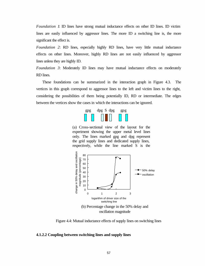
57
Foundation 1: ID lines have strong mutual inductance effects on other ID lines. ID victim
lines are easily influenced by aggressor lines. The more ID a switching line is, the more
significant the effect is.
Foundation 2: RD lines, especially highly RD lines, have very little mutual inductance
effects on other lines. Moreover, highly RD lines are not easily influenced by aggressor
lines unless they are highly ID.
Foundation 3: Moderately ID lines may have mutual inductance effects on moderately
RD lines.
These foundations can be summarized in the interaction graph in Figure 4.3. The
vertices in this graph correspond to aggressor lines to the left and victim lines to the right,
considering the possibilities of them being potentially ID, RD or intermediate. The edges
between the vertices show the cases in which the interactions can be ignored.
Figure 4.4: Mutual inductance effects of supply lines on switching lines
4.1.2.2 Coupling between switching lines and supply lines
(a) Cross-sectional view of the layout for the experiment showing the upper metal level lines only. The lines marked gpg and dpg represent the grid supply lines and dedicated supply lines, respectively, while the line marked S is the
gpg dpg S dpg gpg
0
10
20
30
40
50
60
70
80
0 1 2 3
logarithm of driver size of the switching line
chan
ge in
50%
del
ay a
nd o
scill
aito
n m
agni
tude
(pe
rcen
tage
)
50% delay
oscillation
(b) Percentage change in the 50% delay and oscillation magnitude

58
In the next set of experiments, the experimental setup is similar to Section 4.1.2.1, except
that there is only one switching line that lies between two dedicated supply lines, as
shown in Figure 4.4 (a). Initially the switching line forms one cluster and the two
dedicated supply lines are modeled as RC-only. The driver sizes of the switching line are
set to 5×, 50×, 100× and 200× of the minimum driver size. After the application of CMI
operations on the cluster and the two dedicated supply lines, the changes in the 50%
delay and oscillation magnitude of the switching line are shown in Figure 4.4 (b).
It is observed that the RC model fails as the driver size is increased since inductive
effects become prominent. The inclusion of mutual inductances between the switching
line and the supply lines permits a nearby current return path for the switching lines and
greatly reduces the inductance effect of the ID line, both in terms of delay and
oscillations. The reason is that if there is a supply return path nearby (instead of, for
example, at infinity as assumed by the PEEC model), the magnetic field vector Bv and
magnetic vector potential Av of the aggressor cluster are strongly weakened by the
magnetic field induced by the supply return path. The magnetic vector potential drop
along the victim line, as well as the inductance effect of the aggressor cluster on the
victim line, is also greatly reduced. However, if the switching lines are highly RD lines
(for example, a driver size of 5×), supply lines have little effect on these parameters.
From the simulation results, we can infer the second set of foundations:
Foundation 4: Supply lines have significant mutual inductance effects on nearby ID lines,
which greatly reduces the inductance effect of ID lines.
Foundation 5: Supply lines do not have significant mutual inductance effects on RD
lines.
4.1.3 Formation of clusters
Based on the above foundations, we separate the six possible combinations of mutual
inductance interactions between ID lines, RD lines and supply lines into two classes:
2 Strong mutual inductance interactions between
• ID lines and nearby ID lines
• ID lines and nearby supply lines
3 Weak mutual inductance interactions between

59
• ID lines and nearby RD lines
• Moderately RD lines and nearby supply lines
• Moderately RD lines and nearby moderately RD lines
• Supply lines and nearby supply lines
Since strong mutual inductance interactions are the most important, the proposed
algorithm first identifies strong mutual inductance terms and forms clusters, and then
adds weak mutual inductance terms into those clusters if necessary. In order to reduce as
many of the mutual inductance terms as possible, the proposed algorithms always find the
supply return paths for a cluster before we determine which other clusters or RD lines it
will affect. On the other hand, if we consider the mutual inductance effect between the
aggressor cluster and victim cluster/line without incorporating the effect of the supply
return path, it is very possible that we may overestimate the inductance effect of the
aggressor cluster and include more interactions than is necessary (and consequently
reducing the sparsification).
BASIC STEPS: We proceed by selectively including a new set of inductive effects in
each iterative step. There are four basic steps in the two algorithms in this work, and each
of these steps is typically applied repeatedly, a number of times:
4 Use the ID criterion to check whether a switching line is an ID line or not and form a
preliminary set of clusters, each of which consists of a single ID line.
5 Check whether a single supply line is one of the return paths for a cluster by applying
CMI on the cluster and the supply line. If CMI shows a large mutual inductance
effect, the supply line is an important current return path and should be included into
the cluster. If the cluster only includes one ID line, only strong interactions are
considered in this step; otherwise, both strong and weak interactions are considered.
6 Check whether a single RD line is greatly influenced by a cluster by applying CMI on
the cluster and the RD line. If there is a large mutual inductance effect, the RD line
should be included into the cluster. Only weak interactions are considered in this step.
7 Check if two clusters created so far have important mutual inductance effects between
each other by applying CMI on these two clusters. If all lines in the two clusters are
ID lines and their associated supply return paths, the interactions considered here are

60
strong interactions; otherwise, both strong and the weak interactions are taken into
account in this step.
The above basic steps consider the circuit structure and interconnections between
circuit elements and form the basis for the circuit-aware algorithms. A critical issue is to
determine which supply lines, RD lines and other clusters on chip should be tested for the
CMI operation with a given cluster. The following section describes a method to choose
candidate lines and clusters, which greatly reduced the number of tests needed to be
performed. The lines and clusters found by the method have a large possibility of having
a significant mutual inductance interaction with the cluster in consideration.
Figure 4.5: An example showing three concentric spheres, S1, S2 and S3 outside a cluster
C. The darkness of each sphere represents the likely significance of inductance effect of
lines in that sphere on the cluster.
4.1.4 Choosing candidate lines and clusters for the cluster in consideration
In basic steps 2, 3 and 4, the interaction between any given cluster C and supply lines,
RD lines and other clusters must be checked to see any of them are coupled with C. The
detailed process is described below for the case of supply lines as an example.
For the cluster C under consideration, we divide the region outside of the cluster into
a set of concentric spheres Si with inner radius Ri_in, outer radius Ri_out and thickness ∆R =
Ri_out - Ri_in, as shown in Figure 4.5. The inner radius of sphere Si+1 is the same as the
outer radius of sphere Si and all of the spheres share the same thickness except the
Rs ∆R ∆R •
Cluster C
Concentric spheres
S1
S2
S3

61
innermost sphere. The innermost sphere with radius Rs is centered at the cluster, and is
the only sphere that is not hollow inside.
Checking for supply return paths starts from the nearest supply line to the cluster in
the smallest sphere. Suppose there are Ni supply lines in sphere Si with the first one
nearest to cluster C and the Nith farthest from the cluster, we start the checking with the
first supply line by applying CMI on cluster C and the supply line. If the supply line has a
strong effect on the cluster, then it is added into the cluster temporarily7 and CMI is then
applied on the enlarged cluster and the next nearest supply line; otherwise, CMI is
applied between cluster C and the next nearest supply lines. If we do not make this
temporary addition to the cluster, it is possible that we will overestimate the number of
supply lines needed by the cluster. If there is at least one supply line in sphere Si that has
a strong influence on the cluster C at the center, we test the next sphere Si+1. If there is no
supply line in Si that is important, we conclude that no other supply lines in spheres larger
than Si are important and the check for supply return paths for cluster C is concluded.
This procedure uses an inherent assumption that the nearer the supply line is to the
cluster, the larger its effect on the cluster is likely to be. The rationale for using this
assumption is that nearer supply lines have larger values of mutual inductance with
cluster C, so that they are most likely to influence the inductive behavior of the cluster.
This is also empirically observed. This assumption may not always be correct since it is
very possible that a supply line that is a little nearer to the cluster does not have a large
effect, perhaps because of its large line resistance, while a supply line that is a little
farther away has large effect on the cluster. To overcome this problem in a simple way,
the above process with the concept of spheres with thickness ∆R is utilized. Therefore,
even if in the extreme case, where only the farthest supply line in sphere Si has a strong
effect on cluster C while the other supply lines in that sphere have no large effect on C,
the supply lines in sphere Si+1 just outside Si will still be checked according to the process
described above.
The effectiveness of this process depends on the value of Rs and ∆R. If Rs and ∆R are
rather large, then all of the supply lines on the chip may be checked, so that this process
7 The reason why these additions are considered “temporary” is that whenever a new cluster is considered, even supply lines that were previously incorporated into another cluster are taken to be candidate return paths. As a result of this, the clusters that are formed do

62
brings us no error in the way of choosing supply lines. However, this is computationally
expensive. On the other hand, if there is only one line in each sphere, then perhaps only
one supply line may be checked, which is clearly an incorrect analysis for a design with
poorly placed return paths. However, for a good design where supply lines are effective
and the magnetic field is localized tightly at nearby region of a cluster, even one supply
line per sphere may work well. The values of Rs and ∆R are user-specified.
The above process is used not only in the step of finding supply return paths, but also
used in the steps that find RD lines and other clusters that cluster C influence. The only
differences in the process for the latter two steps are that the candidates for addition to C
are not supply lines, but RD lines and/or clusters, and if these have a strong interaction
with cluster C, they are not temporarily grouped into C. The addition of RD lines and/or
other clusters into cluster C will strengthen the cumulative magnetic field of cluster C,
which in turn may need more supply return paths to be added to C to weaken this
magnetic field; if we were to add RD lines and/or other clusters into cluster C without
looking for more supply return paths before checking for inductance effect between this
enlarged cluster and other RD lines and/or clusters, it is possible that we would
overestimate the inductance effect of cluster C.
In the succeeding sections, we present two algorithms for creating clusters that use
the above framework.
4.2 Circuit-aware Algorithm 1
4.2.1 Description of Algorithm 1
From the previous discussion, it is clear that the main idea in the circuit-aware algorithm
is to find the most important inductance terms first, followed by heuristically adding
weak inductance terms into clusters, so that the clusters increase in size until they do not
grow any more. The algorithm always tries to drop off as many unimportant inductance
terms as possible.
The oscillation on the supply lines because of the high pad impedance, the switching
current drawn by the functional blocks connected to supply lines and the mutual
inductance effects of nearby switching lines all serve to reduce the integrity of supply
not depend on the sequence in which the original clusters were processed and some supply lines may be temporarily assigned to more

63
lines, which can potentially impact the output response significantly. Therefore, if the
objective is to obtain high accuracy modeling, we should realistically consider the RKC’s
associated with the supply lines. Algorithm 1 is a circuit-aware algorithm that operates
under such a model for supply lines, where the magnetic field of switching lines is
considered to be capable of reaching infinity (or more realistically, the chip-size) and
influencing the response of other switching lines and the integrity of faraway supply
lines.
Algorithm 1 is a combination of the basic steps described in Section 4.1.3, as depicted
in the flow chart in Figure 4.6. It is an iterative method in which the output response is
brought closer to the accurate response in each iteration. The algorithm begins by using a
RC model for all lines. After applying the ID criterion, each ID line forms a cluster,
called an ID cluster, with only one line in it. It is worth pointing out that throughout the
algorithm, each cluster includes at least one ID line.
Once this is done, we would like to attempt to combine clusters taking into account
strong interactions between pairs, a pair of clusters at a time. However, as stated earlier,
return paths through nearby supply lines may greatly reduce the inductive effects of a
cluster as calculated from the partial inductances, and consequently, the strong
interactions of the cluster with other clusters. Therefore, it is important to first consider
interactions between a cluster with nearby supply lines8. We will refer to the set of
clusters at the beginning of this step as the “original clusters.”
The method for finding the supply return paths9 is outlined as step 2 in Section 4.1.3
and in Section 4.1.4. The choice of the supply line to be included in the original cluster is
heuristically made by selecting the nearest supply lines one at a time and applying step 2,
possibly enlarging the cluster after each such line is considered.
Although this process potentially enlarges each cluster by adding to it a set of supply
lines, these additions are considered “temporary”, i.e., before we find the supply lines for
a new cluster, all of those supply lines which are temporarily added into the previous
cluster are recorded and then released.
than one cluster. 8 If supply line interactions are not considered before other interactions, the algorithm will not result in incorrect results, but it may be unduly pessimistic and may create larger clusters than is necessary, leading to less sparse K matrices. 9 Note that this does not imply that these are the only return paths; other return paths are identified later.

64
Once all of the original clusters have been processed, new ID clusters are formed by
first enlarging each ID cluster by adding to it the supply return paths determined above.
Next, any two clusters that share a line are grouped into a larger cluster in order that all
mutual inductances can be considered, and no inductance terms are truncated.
The next step after finding supply return paths is to check if two ID clusters have a
strong mutual inductance interaction between them. The process of checking strong
interaction between ID clusters is described in step 4 in Section 4.1.3 and Section 4.1.4.
The clusters that have strong interactions are grouped into larger clusters. Again, to avoid
the pitfalls associated with truncating inductance values, two clusters that have a strong
interaction with at least one common cluster are combined into the same cluster, even if
they do not mutually have a strong interaction. The above process of finding supply
return paths and finding strong interactions are repeated until no new mutual inductance
interactions are found and no new clusters are formed. At the end of this process, all of
the strong mutual inductance interactions have been identified.
Next, we check for weak mutual inductance effects that correspond to the interaction
between two nearby clusters or between one cluster and one nearby RD line. Before
checking for this, additional return paths should be identified for each cluster using a
technique that is similar to that used for the original clusters. To identify these weak
mutual inductance interactions, we apply the method described in steps 3 and 4 in Section
4.1.3 along with the technique in Section 4.1.4. The above process of finding additional
supply return paths and finding weak interactions among clusters and RD lines is
repeated until no new mutual inductance interactions are found and no new clusters are
formed.
In this way, all the important inductance terms are included in final clusters with a
high sparsification.

65
Figure 4.6: A flowchart that describes Algorithm 1.
4.2.2 Computational cost of the circuit-aware algorithms
To evaluate the computational cost of the proposed algorithms, consider a circuit with N
lines, which have at most nseg segments on each line. It can be seen in Figure 8 that there
RC model for all lines
Find ID lines and form ID clusters
Find supply return paths for each ID cluster
Group ID clusters
New clusters formed?
Look for additional return paths for each cluster
Group clusters Group clusters and RD lines
No
Yes
New clusters formed?
Exit
Yes
No
Find strong interactions
Find weak interactions

66
are three main parts in the circuit-aware algorithm: finding ID lines, finding strong
interactions and finding weak interactions. Since the first part processes each line
individually, its cost is linear in the number of lines, and hence, the latter two parts are
dominant in the total computational cost. We estimate their complexity under reasonable
assumptions as follows.
In the worst case, all lines are initially identified as ID, and all of these lines
eventually are added into the same cluster, with one line being added into the cluster in
each iteration. Without loss of generality, let us assume that after the first iteration, the
first and the second ID lines are grouped into an intermediate cluster with two lines in it,
while all the other ID lines are kept alone in their own cluster; after the third iteration, the
third ID line is added into the intermediate cluster, which now has three lines in it, while
the other ID lines are alone as before, and so on. Therefore, after N-1 iterations all lines
are grouped into one final cluster, and the upper bound of the total number of iterations is
O(N). Suppose nCMI is the upper bound on the number of CMI operations for each cluster;
practically, this is seen to be bounded by a constant.
The computational cost of one CMI operation between two original clusters is
O(nseg), so that the cost in the first iteration is O(nCMI×N×nseg). In the second iteration,
there are N-1 clusters, of which one cluster is the enlarged intermediate cluster with at
most 2×nseg segments in it, while the other clusters are still the lone ID lines, each with at
most nseg segments. One of these ID lines is now added to the cluster in the second
iteration, with a computational cost of O(nCMI× (N-2) ×nseg+ nCMI×2×nseg) =
O(nCMI×N×nseg), which is the same as the computational cost for the first step. The same
conclusion can be derived for the third iteration, the forth iteration, and so on. Therefore,
the total complexity for N iterations is O(nCMI×N2×nseg).
In practice, the number of iterations is much smaller than N. If the total number of
iterations can be bounded by a constant, the complexity will be O(N×nCMI).
4.3 Implementation of K-PRIMA
As stated in Chapter 1, we use the K element [17] to represent the inductance system in
the proposed algorithm. This is based on the idea of representing inductive effects using
the inverse of the inductance matrix. We adapt the PRIMA algorithm [19] in order to

67
generate a simulator, K-PRIMA, which can work with K elements and guarantee the
passivity of the reduced system. This simulator is used numerous times in the algorithm,
twice in each CMI operation. Starting with the traditional inductance matrix M,
simulation in each step of algorithm requires solving the following system of differential
equations, which are formed using the Modified Nodal Analysis (MNA) approach:
BxsCG =+ )( (4.1)
−
=0TE
ENG
=
M
QC
0
0
=
i
vx (4.2)
where (G+sC) is the admittance matrix, x is a vector of unknown node voltages and
unknown currents of inductors and voltage sources, B is a vector of independent time-
varying voltage and current sources, and M is the traditionally used inductance matrix. In
order to guarantee passivity, a sufficient condition [19] is to ensure that the off-diagonal
submatrices have a negative transpose relation in the G matrix and that N, Q, and M be
symmetric and positive definite. In order to introduce K matrix into (4) and at the same
time satisfy the above requirement, the second set of equations implied by (4) are adapted
as follows:
0=+− sMivET (4.3)
Since M is symmetric and positive definite, it can be Cholesky-factored as M = L LT.
Substituting this Cholesky factorization in (4.3) above, we obtain
0=+− isLLvE TT (4.4)
Premultiplying (4.4) by L-1, we get
01 =+− − isLvEL TT (4.5)
Now we define bT iiL = and rewrite (4.5) as
01 =+− −b
T sivEL (4.6)
The first set of equations in (4.1) can then be rewritten as
bsQviLENv bT =++ −1)( (4.7)
Therefore, from (4.6) and (4.7) the MNA matrix can be written as:
−=
−
−
0
)(1
1
T
T
EL
LENG
=I
QC
00
=
biv
x (4.8)

68
It can be verified that the construction of (4.8) satisfies the requirements of preservation
of passivity of PRIMA as described in [19], since the proof of passivity in [19] requires
the off-diagonal blocks in G to be negative transposes of each other.
Since 1111 )()( −−−− === LLLLMK TT , L-1 is also a factor of K matrix and both
K and L-1 have the property of locality. The proposed approach to find the sparsified L-1
is adapted from the method to find Kall matrix described in [17]. A further simplification
is possible: the K submatrix for each cluster is built independently of the other clusters
since there are no mutual inductance terms between clusters. Therefore, in constructing
the window for finding the submatrix of K for a given cluster, it is necessary only to
consider wires within the cluster. This allows greater adaptability: the window sizes and
shapes may be different for different clusters since the windowing operations are applied
to different clusters independently.
The following is the approach to construct the sparsified L-1 matrix (the notation used
here is similar to [17]):
8 For each aggressor line segment i, find a traditional inductance matrix Msmall
including the line segments that lie within the cluster that i belongs to and lie within
in a small window size around i.
9 Cholesky-factorize Msmall to find the Cholesky factor Lsmall, which is a lower
triangular matrix.
10 Invert Lsmall.
11 Compose the large system L-1 by the column corresponding to the aggressor line
segment in 1−smallL .
Using this approach, the K and L-1 matrices can be greatly sparsified and save a large
amount of computational cost.
4.4 Circuit-Aware Algorithm 2
Algorithm 1 applies to the most realistic case with imperfect supply lines. However, for a
very well designed supply grid or in cases where the requirement to the accuracy of
modeling is not very high, the ∑j
jij dtdIL )/( drop on the supply grid can be assumed to
be zero and the supply grid can be assumed to be perfect in this respect. However, we

69
point out that we do consider the RC drops in supply lines, and that we do not consider
the supply lines to be perfect ground planes. Algorithm 2 is another version of the circuit-
aware algorithm with such an assumption and is developed as an extension of Algorithm
1. Specifically, we assume that the currents return from the supply lines within a user-
defined distance. Within this distance, we assume that the ∑j
jij dtdIL )/( drops on the
supply lines are zero (but the RC drops could be nonzero), while outside this distance, the
net magnetic field of the aggressor lines and the return currents is zero. A similar
assumption was also made in the work in [23] and apart from the fact that [23] is not
circuit-aware, a primary difference between the proposed work and theirs is that we allow
currents to return from the supply lines beyond the nearest supply lines, so that the
switching lines can have mutual inductance coupling with other switching lines beyond
the nearest supply lines, unlike [23], which assumes that the currents return from the
nearest supply lines and that the switching lines in different interaction regions defined
by “halo rules” are completely decoupled. In reality, only a perfect, infinitely large
conductor plate can fully decouple the magnetic field and an on-chip metal line only
partially blocks the magnetic field. This weakened magnetic field can influence the
switching lines outside the nearest supply lines, and except in a very good design, such an
influence can reach far away.
For a good or reasonable design, we employ a user-defined distance to describe how
far the magnetic field can still have strong effect. This distance is defined on the group of
switching lines, called the aggressor group, between the nearest supply lines and used as
an approximation order. Under the above assumption, Algorithm 2 generates a new and
equivalent inductance system Ms by removing mutual inductance terms explicitly related
to supply lines from the original system M and incorporating the effect of supply lines
into the inductance values of Ms. By construction, we ensure that Ms is symmetric and
positive semidefinite. Algorithm 1 is then applied to the new inductance system with a
little adaptation. Figure 4.7 shows a schematic of a small example with two aggressor
lines i and j. The aggressor groups they belong to and the corresponding user-defined
distances up to which the influence of the magnetic field of the aggressor group can reach

70
are shown in the figure. For ease of identification, the supply lines are shown to be longer
and thicker than the signal lines in the schematic.
Figure 4.7: A schematic showing a set of aggressor lines, aggressor groups and the user-
defined distances. The dashed line shows the user-defined distance for aggressor group
gi, while the dash-dot line is the user-defined distance for aggressor group gj.
4.4.1. Definition and formation of the new matrix Ms
For a layout including both supply lines and switching lines, the device equation of
inductors can be written as
=
s
pgT
s
pg
II
MMMM
sV
V
2212
1211 (4.9)
where Vpg and Vs represent the voltages difference across line segments on supply lines
and switching lines, respectively, Is and Ipg are the currents in these line segments on the
switching and supply lines, respectively, and M11, M12 and M22 are inductance
submatrices. For ease of exposition, we will work with the inductance matrices here
instead of the K matrices, although the implementation uses the K matrix representation.
Since the supply lines are assumed to have no ∑j
jij dtdIL )/( drop, Vpg should be the
zero vector. Therefore, the first set of equations can be written as:
Aggressor group gi
line i
User-defined distance of aggressor group gi
line j
Aggressor group gj
User-defined distance of aggressor group gj

71
spg IMMI 121
11−−= (4.10)
Substituting (4.10) into the second set of equations yields
sssT
s IsMIMMMMsV =−= − )( 121
111222 (4.11)
The calculation of Ms can be very efficient since M is symmetric and positive
semidefinite and can be Cholesky factored as:
TT
TT
T LLL
LLLL
L
MM
MMM =
=
=
22
2111
2221
11
2212
1211
0
0
A few algebraic manipulations lead to the result
121
111222 MMMMM Ts
−−=
TTTTT LLLLLLLLLL 21111
1111112122222121 )( −−+=
TLL 2222= (4.12)
Since L22 and L22T are triangular matrices, the computation for (4.11) is greatly reduced.
It is easy to prove that the new inductance matrix Ms is symmetric and positive
definite. We can think of Ms as a partial inductance matrix for a new inductance system,
and as a substitute of the original system M, but with better locality properties. This
locality provides further sparsification above and beyond that obtained by dropping the
inductance terms explicitly related to the supply lines.
Figure 4.8: A layout example of six 600µm -long lines. The lines marked P/G represent
the power/ground (supply) lines, while those marked S1 through S4
are the switching lines.
4.4.2 Locality of matrix Ms
We now present an example to demonstrate the locality of the Ms matrix. The layout
includes six parallel lines as shown in Figure 4.8. Both the width and the spacing of each
line are 0.9µm and the height of each line is 0.5µm. Each line is cut into ten line
P/G S1 S2 S3 S4 P/G
Length=600µm

72
segments with 60µm per segment. The first and sixth lines, marked P/G, are supply lines,
while the other four lines, S1 through S4, are switching lines.
The mutual inductance matrix M, a 60×60 matrix, is calculated using GMD formulæ
for partial inductances. Here we only show a part of M to demonstrate how the value of
mutual inductance is changed under the assumption of zero inductive drops on the supply
lines. The columns of M correspond to the first three consecutive line segments of S1,
followed by the first line segment of S2, S3 and S4, respectively. The first line segment
on each line faces the first line segment on its nearest lines. The matrix Ms is obtained
using the procedure described above.
=
4.598.308.3006.372.72.268.304.598.3006.389.78.308.309.384.5906.307.89.38
06.306.306.34.5924.806.372.789.707.824.84.5924.8
2.268.309.3806.324.84.59
M pH (4.13)
=
1.328.1554.907.045.039.58.157.387.1809.064.055.9
54.97.187.3809.073.08.1507.009.009.01.3268.007.045.063.072.068.01.3269.039.555.98.1507.069.01.32
sM pH (4.14)
From (4.13) and (4.14) we can see that the value of M11 in Ms matrix, the self-inductance
of the first line segment on S1, is only 54% of that in M matrix. M12 in the Ms matrix, the
mutual inductance between the first line segment and its nearest neighbor segment on the
same line, is 2% of M11 in the Ms matrix, while this value is 13.8% in the M matrix. M16,
the mutual inductance between the first line segments on S1 and S4 are 44% and 16.8%
of M11 in M and Ms matrix, respectively. The large reduction in the self and mutual
inductance of line segments is due to the effect of supply lines as current return paths on
the magnitude of the magnetic field of the switching lines. However, the great reduction
of inductance values in this example does not mean that the nearest supply lines are
enough to block the magnetic field of the aggressor lines in any circuit environment.
Such an assumption is only accurate when the circuit is very well designed with excellent
return paths and/or when the desired accuracy is not so high.

73
4.4.3 Description of Algorithm 2
Algorithm 2 is summarized in Figure 4.9 and is actually a more computationally efficient
version of Algorithm 1. Unlike Algorithm 1, this algorithm do not work with the supply
lines to add return paths to the cluster, because all of the important supply return paths
are assumed to lie within the user-defined distance of an aggressor group. These supply
lines are removed from the M matrix by the technique described in Section 4.4.1, with the
effect of supply return paths being incorporated during the calculation of the Ms matrix.
All of the other steps in Algorithm 1 are used here except that each inductance value
comes not from the original system M, but from the Ms matrix.
12 Use the new values of self and mutual inductance in Ms to find ID lines, and form ID
clusters using the ID criterion.
13 Check all ID clusters to see if any two of them should be grouped into one larger
cluster. At the end of this process, if any two of the newly formed clusters have
common lines, group them into one cluster. Repeat step 2 until no new cluster is
formed.
14 Test to see if any two clusters, or one cluster and one RD line, should be combined
into one cluster. At the end of this process, if any two of the newly formed clusters
have common lines, group them into one cluster. Repeat step 3 until no new cluster is
formed.
Figure 4.9: Outline of Algorithm 2
4.5 Experimental results
We have carried out a set of experiments to examine the correctness of the assumptions
and the effectiveness of the proposed algorithms. Specifically, we study the effect of
dedicated supply lines on reducing inductive effects, compare the results of Algorithm 1
and 2, compare Algorithm 1 with the shift-and-truncate method and demonstrate the
effect of altering the user-defined distance in Algorithm 2. We also analyze the results to
outline techniques for optimizing inductance effects. All of the experiments carried out in
this work are on a 0.1µm technology, and the corresponding parameters are extrapolated
from [60]. These parameters are summarized as follows:

74
Minimum line width= 0.1 µm
Driver resistance for minimum buffer size=23.9 KΩ
Minimum line spacing=0.14 µm
Driver input capacitance for minimum buffer size=0.07 fF
The circuit topologies correspond to the top three metal layers, M5, M4 and M3, of a
five layer metal structure, with wide and long switching lines being routed on the
uppermost metal layer. Supply lines in the vertical direction are routed in M5 and M3,
while those in the orthogonal direction are on M4. The circuit topologies used in this
section are based on the models and layer assignments described in Chapter 2, and in all
cases, a voltage swing of 1V is used.
4.5.1 Comparison of the accuracy of Algorithms 1 and 2 with the exact response
Two sets of experiments are performed in this section on two different configurations to
compare the effectiveness of Algorithms 1 and 2 with each other. The cross sections of
the layouts of Circuit 1 and 2 are as shown in Figure 4.10. In Circuit 1, there are 10
vertical grid supply lines in M5, with 8 switching lines and 3 dedicated supply lines
between the 5th and 6th grid supply lines. There are 10 vertical grid supply lines on M3
and 21 horizontal grid supply lines on M4. The driver sizes of the 8 switching lines
named, from left to right, S1 through S8, are 100×, 200×, 10×, 100×, 100×, 5×, 50×, and
200×, respectively. The three dedicated supply lines are positioned, respectively, to the
left of the first switching line, between the fourth and fifth switching lines, and to the
right of the eighth switching line. Circuit 2 is identical to Circuit 1 in all respects, except
that all dedicated supply lines are removed, so that it is a “worse” design than Circuit 1.

75
(a)
(b)
Figure 4.10: Cross sectional views (not drawn to scale)
of the layouts of (a) Circuit 1 (b) Circuit 2.
Figure 4.11: Comparison of the output response with the accurate response for Circuit 1.
The solid line shows the accurate response, the dashed line the response after applying
Algorithm 1 and the dash-dot line the response after applying Algorithm 2 with the user-
defined distance set to be the second nearest supply lines.
M5 M4 M3
Signal lines S1 to S4
Dedicated supply lines
Dedicated supply lines
Signal lines S5 to S8
M5 M4 M3
Signal lines S1 to S8
Grid supply lines
Grid supply lines

76
In Circuit 1, the simulation results for the second switching line, which is one of the
farthest switching lines from the dedicated supply lines and shows the largest inductance
effect, are displayed in Figure 4.11. The waveforms shown correspond to the accurate
response that considers all the inductance terms, to Algorithm 1, and to Algorithm 2. For
the latter, two sets of user-defined distances are tested: in the first, this is set to be until
the second nearest supply lines, i.e., all of the three dedicated supply lines are within the
user-defined distance of each aggressor group, while in the second, the limit is set to be
the nearest supply lines. The errors in the 50% delay and oscillation magnitudes in all
cases are summarized in Table 4.1. The ε for the oscillation magnitude and the δ for the
50% delay used in CMI operations are 10% and 5% respectively.
Algorithm 2 Accurate
response Algorithm 1 Nearest
supply lines Second nearest
supply lines 50% delay (ps) 9.4 9.8 3.7% 8.5 9.5% 8.8 6.3%
Oscillation magnitude (mV) 170 160 5.8% 110 35% 130 23.5%
Table 4.1: Oscillation magnitudes and 50% delays from the accurate response, from
Algorithm 1, and from Algorithm 2 with the user-defined distances set to be the nearest
supply lines or the second nearest supply lines. The relative errors are obtained from the
comparison with the corresponding values in the accurate waveform.
The accurate waveform in Figure 4.11 is shown by the solid curve and yields a delay
of 9.4ps and an oscillation magnitude of 170mV. Compared with the accurate response,
the error in the 50% delay obtained by Algorithm 2 with the second nearest supply lines
as the user-defined distance is only 6.3% but the error in the oscillation magnitude can
reach 40mV, which is about 23% of the accurate value. In comparison, Algorithm 1 is
more accurate in the oscillation magnitude with the error within 10mV. As a compromise
to the higher accuracy, the sparsification of Algorithm 1 is a little lower.
The larger error in the oscillation magnitude between the accurate waveform and that
from Algorithm 2 implies that its underlying assumptions about the supply lines may not
be good if a high accuracy in oscillation magnitude is desired in this circuit; however, it

77
is acceptable if the objective is to find the delay rather than the entire waveform, and
these assumptions result in a higher sparsification. The results are consistent with the
observations in [23], which sets the user-defined distance to be the nearest supply lines.
The error in overshoot shown in [23] is about 45% (which is higher than the numbers that
we observe), but the 50% delay is matched very well. Therefore, if the aim of the
simulation is to obtain the correct delay in this circuit, Algorithm 2 is sufficiently
accurate; however, if the purpose is to obtain accuracy on both the delay and the
oscillation magnitude, Algorithm 1 can be applied.
From Table 4.1, it is very clear that the larger user-defined distance improves the
accuracy of Algorithm 2. The reason is that the ideal supply line assumption with zero
∑j
jij dtdIL )/( drop will not fully block the magnetic field of the aggressor group, but
only weaken the coupling between the two aggressor groups. Therefore, ignoring the
magnetic coupling between the two aggressor groups may cause a large error in the
oscillation magnitude. It is expected that if there are more aggressor groups nearby, this
error may be even larger and the necessary user-defined distance would be accordingly
larger.
Figure 4.12: Schematic diagram showing the highlighted aggressor line segment i,
and line segments in its window for Circuit 1 in Algorithms 1 and 2.
Aggressor line segment i
Window of segment i in Algorithm 2
Nearest dedicated supply lines
Switching line segments
Window of segment i in Algorithm 1

78
As stated in Section 5.1, the sparsified L-1 matrix is constructed by finding the
inductance matrix in a small window for each aggressor line segment. Figure 4.12 is a
schematic showing the line segments, all of equal length, that are included in the window
of the aggressor line segment i in Algorithm 1 and Algorithm 2 for Circuit 1. Rs, the
radius of the smallest sphere (defined in Section 3.4) when we choose the candidate lines
and clusters, is 30µm and ∆ R, the sphere thickness, is chosen to be 60µm. The window
size for segment i found by applying Algorithm 1 on Circuit 1 is such that in the direction
of the lines, each segment only has a mutual inductance with the line segments nearest to
it, while in the perpendicular direction, the window size is 25µm (i.e., the line segment
has mutual inductance with other segments whose distance to segment i is less than
25µm). On the other hand, the application of Algorithm 2 finds that the mutual
inductances of the nearest line segments and the second nearest line segments on the
same line must be included in the window size for higher accuracy in the oscillation
magnitude.
Figure 4.13: Cluster formations for Circuit 1 in Algorithm 1 (upper) and 2 (lower).
M5 M4 M3
Cluster 1 including S1, S2 and S4
Cluster 2 including S5, S7 and S8
M5 M4 M3
Cluster including S1, S2, S4, S5, S7 and S8, three dedicated supply lines and two grid supply lines

79
Figure 4.14: Cluster formations for Circuit 2 in Algorithm 1 (upper) and 2 (lower).
Two basic clusters for Circuit 1 in Algorithm 2 are formed as shown in Figure 4.13,
with S1, S2 and S4 (with driver sizes of 100×, 200× and 100×, respectively) between the
first and second dedicated supply lines being placed in one cluster, and S5, S7 and S8
(with driver sizes 100×, 50× and 200×, respectively) between the second and third
dedicated supply lines in the second cluster. Lines S3 and S6, driven by 5× and 10×
drivers, respectively, are modeled using RC only. For Algorithm 1, all of the switching
lines, except lines S3 and S6, as well as the three dedicated supply lines and the nearest
grid supply lines are included in one basic cluster, because the dedicated supply lines are
shared by these switching lines.
It should be pointed out that imperfect integrity obtained from, for example,
providing inadequate return paths, plays a significant role both in the inductance effects
in a circuit and in the sparsity that can be obtained. To observe this, consider Circuit 2,
which is a worse design of Circuit 1 due to the removal of all three dedicated supply lines
(but not the grid supply lines). The inductance effects of the ID lines cannot be
effectively reduced by supply lines. The oscillation magnitude of the second switching
line jumps to 371mV and the 50% delay increases to 14.2ps. For Algorithm 1, if the same
level of accuracy is maintained, the window size in the direction of the lines increases to
M5 M4 M3
Cluster including all the switching lines
M5 M4 M3
Cluster including all the switching lines, and eight grid supply lines

80
two (i.e., each segment has a mutual inductance with the line segments nearest to and the
next nearest to it), and in the perpendicular direction it is 70µm. The clusters formed by
Algorithm 1 and 2 for Circuit 2 are shown in Figure 4.14. Even the mutual inductance
with lines that would have been expected to be highly RD (such as lines S3 and S6) must
be considered for the accurate modeling of the response of RD lines, and a larger number
of grid supply lines must be included into clusters.
4.5.2 Sparsification comparisons
In this section, we compare the sparsification obtained from Algorithm 1 and the shift-
and-truncate method under the same accuracy for four circuit Circuit 1, 2 3 and 4,
summarized in Table 4.2, which also includes the results from Algorithm 2.
Circuit 1 Circuit 2 Circuit 3 Circuit 4 Algorithm 1 97% 87% 97% 83% Algorithm 2 99% 98% 98.4% 97%
Shift-and-truncate 92.5% 75% 90% 68%
Table 4.2: Sparsification from Algorithm 1, Algorithm 2 and
the shift-and-truncate method in Circuit 1, 2 3 and 4.
For a good design such as Circuit 1, Algorithm 2 achieves 99% sparsification, while
the corresponding figure for Algorithm 1 is 97%, which is expectedly lower since the
latter is the more accurate algorithm. It was found that for both of the circuit-aware
algorithms, the sparsifications for Circuit 2 are worse than those for Circuit 1. For
Algorithm 2, if the sparsification is still relatively high at 98%, the error in the 50% delay
reaches 12% and the error in the oscillation magnitude is larger than 150mV. For
Algorithm 1, if we still obtain 15% error in the oscillation magnitude and 10% error in
delay, the sparsification is found to be 87%. Under the same accuracy, the corresponding
sparsification for the shift-and-truncate method was found to be lower, at 75%.

81
(a) (b)
Figure 4.15: Cross sectional views of (a) Circuit 3 and (b) Circuit 4.
A further comparison was performed on two more circuits. Circuits 3 and 4 are a pair
of layouts illustrated in Figure 4.15, of which Circuit 3 is good design and Circuit 4 is a
poor design without the dedicated supply lines to effectively reduce inductance effect of
ID lines. Circuit 4 has 16 vertical grid supply lines in M5, with 4 switching lines
between the 8th and 9th grid supply lines. There are 7 horizontal grid supply lines on M4
and 16 vertical grid supply lines on M3. The driver sizes for the 4 switching lines named,
from left to right, S1 through S4 are 220×, 150×, 200×, 5× times the minimum size,
respectively. There is no dedicated supply line near the switching lines in Circuit 4, while
Circuit 3, which is an optimized version of Circuit 4, has one dedicated supply line each
on the left and right sides of the four switching lines. For Circuit 3, Algorithm 1 yields a
sparsification of 97% while the shift and truncate method has a sparsification of less than
90%. In Circuit 4, the sparsification of Algorithm 1 is 83% and that for shift and truncate
method is 68% with the same accuracy. Both of the algorithms yield much lower
sparsifications on Circuit 4, and this is inherently due to the fact that the design has poor
return paths. The sparsification from Algorithm 2 is still rather high. For Circuits 3 and 4,
these sparsifications can reach 98.4% and 97%.
4.5.3 Interpretation of the results
From the experimental results, we can reach several conclusions. Firstly, for more
accurate modeling, the influence of supply lines should be considered and Algorithm 1
serves as a better method than Algorithm 2 in the aspect of accuracy; however, for delay
estimation purposes only, the latter is adequate. Secondly, under the same accuracy, we
have shown that the shift-and-truncate method yields a lower sparsification compared
M5 M4 M3
Signal lines Grid supply lines
Grid supply lines
M5 M4 M3
Signal lines Dedicated supply lines
Dedicated supply lines

82
with that of Algorithm 1. The major reason is that Algorithm 1 makes effective use of the
circuit-aware method and discards all the inductance terms related to highly RD lines,
such as the 5× and 10× driven lines in Circuit 1, and the terms related to some supply
lines which do not have significant inductive interactions with the switching lines. In
contrast, the shift-and-truncate method computes all of these interactions. Another
contributing factor is that the K element representation provides a higher sparsification
with the same accuracy, as compared to an M element representation. On an average, we
found that roughly 80% of the improvements in sparsity were due to the use of circuit-
aware methods, and 20% to the use of the K matrix instead of the M matrix.
The circuit-aware method also provides pointers on how to optimize inductance
effects in a system. During the procedure, if two clusters are to be grouped into one
cluster, the mutual inductance between these two clusters, especially between ID lines in
each cluster, have strong mutual inductance effect. One way to reduce their inductance
effect is to add some dedicated supply lines next to the ID lines. In this circuit, perhaps
Algorithm 2 can be used to describe this system because the more localized the magnetic
field of ID lines is, the more accurate the results of Algorithm 2 would be. An interesting
conclusion is that reducing inductance effects is not only useful in a circuit context but
also in the ease of analysis.
4.6 Conclusion
Two circuit-aware based sparsification methodologies for fully coupled PEEC K-element
representations for an inductive system are proposed by analyzing the circuit
characteristics and clustering the inductances according to their relative importance to the
circuit. The experimental results show the effectiveness of the circuit-aware method
compared with the shift-and-truncate method. Algorithm 2 works well in a good design
where supply lines behave more perfectly and often gives a high sparsification but a
relatively low accuracy. Algorithm 1 is designed for any circuit and provides a high
accuracy but with a lower sparsification than that of Algorithm 2. The circuit-aware
method helps to determine current return paths for a design and identifies the most
critical inductance terms for optimization.

83
Chapter 5
Table Look-up Based Compact Modeling for On-
chip Interconnect Timing and Noise Analysis
5.1 Background
5.1.1 The hybrid ladder model
An RL ladder circuit can be used to model the impact of frequency dependencies on the
resistance and inductance due to the proximity effect and the skin effect. A commonly
used model was proposed in [39] and is shown in Figure 5.1(a). It has been demonstrated
[38] that this model can be synthesized by knowledge of the equivalent resistance and
inductance at high and low frequencies. The simple RL ladder model was further
developed in that work into a more complex hybrid ladder model as shown in Figure
5.1(b). In addition to the ladder model elements R0, L0, R1 and L1 from Figure 5.1(a), a
shunt circuit of R2 and L2 in parallel with the high-frequency inductance L0 helps to
compensate for the additional reduction of the loop inductance at extremely high
frequencies.

84
(a) (b)
(c1) (d1)
(c2) (d2)
Figure 5.1: (a): The RL ladder circuit. (b): The hybrid ladder model [22].
(c1) and (c2): A simplified ladder model at low frequencies.
(d1) and (d2): A simplified ladder model at high frequencies.
At low frequencies f when R2 >> 2π fL2, R2 >> 2π fL0 and R1 >> 2π fL1, the hybrid
ladder model is simplified to L0 connected in series with the parallel connection of
resistances R0 and R1, as shown in Figure 5.1 (c1). This can be further simplified to
Figure 5.1 (c2) at extremely low frequencies, where the circuit reduces to just R0 in
parallel with R1. Similarly, at high frequencies, when R1 << 2π fL1, R0 << 2π fL1 and R2
<< 2π fL2, the hybrid ladder model is simplified to R0 connected in series with the
parallel connection of the inductances L0 and L2, as shown in Figure 5.1 (d1). This can be
further simplified to Figure 5.1 (d2) so that the equivalent circuit at extremely high
frequencies consists of the inductances L0 and L2 in parallel.
The synthesis procedure in [38] can be summarized as follows. The low-frequency
inductance and resistance, the high-frequency inductance and the cross-over frequency
(where R=2π fcL) are calculated using an RL-only technique that neglects capacitive
L0
R1
R0 L2
L0 R0
R1
R0 L2
L0
R0
L0
L1
R1 L0
L1
R1
R0
L2
R2

85
effects. The model parameters R0, L0, R1, and L1 are then calculated by forcing the low-
frequency inductance and resistance, high-frequency inductance and the crossover
frequency of the model to match the calculated values above. Next, R2 and L2 are
obtained from the resistance and inductance of parallel plate return conductors, if they
exist.
5.1.2 Current distribution patterns
An overview of current distribution patterns and the impact of different circuit elements
on the current return paths have been described in detail in [16]. The model points to the
fact that real current distribution patterns are too complex to be captured by an RL-only
model and depend greatly on the nature of the power grid: in particular, neglecting the
decoupling capacitances and current patterns in the power grid entirely can result in large
inaccuracies for the compact model. To overcome this, we utilize in the characterization
procedure a detailed PEEC based model that includes power grid decoupling
capacitances and power pad placements.
5.2 Outline of the approach
The compact modeling procedure in this work finds circuit parameter values for a two-
path ladder model, described in Section 5.3. This is performed using a nonlinear
optimizer that fits the parameter values to match an exact response from the
comprehensive PEEC model described in Chapter 2 for a set of characterization
structures, under a range of conditions as described in Section 5.4. By performing this
optimization for a variety of circuit topologies, representative structures are characterized
and stored in a table. Subsequently, a compact model for a given structure may be found
by looking up entries in the table, perhaps using interpolation if the stored values do not
exactly match the query to the table. The structure of this table is described in Section
5.2.2.
The proposed approach requires a single characterization step for each design using a
model for the power grid. It has been shown in Table 1 of [61] that for a reasonable
design, even significant changes in the structure of the power grid do not noticeably
influence the response characteristics of the logic. We utilize this fact to work with a

86
representative power grid, under the assurance that to the first order, the proposed model
will remain reasonable even if the actual grid is perturbed from the assumptions under
which the characterizations are performed.
5.2.1 Circuit model for the accurate responses
All of the circuits in this work are four metal layer conductor structures on layers M6,
M7, M8 and M9 of a nine-layer chip. The thickness of these structures is 5µm several
different test structures are characterized, with different signal line lengths, widths and
spacings to the nearest supply line. The power/ground wires are distributed densely in the
four layers. The signal wires are on M8 but the clock nets are distributed on M6, M7 and
M8. A comprehensive PEEC model, described in Chapter 2, is used in order to accurately
estimate the current return paths and inductance effects. In addition to the interconnect
net under consideration, the circuit model includes supply lines, drivers and receivers of
various widths, vias, pads and functional blocks connected to supply lines.
5.2.2 Constructing the look-up table
The model parameters computed by the synthesis procedure are stored in a table. Each
entry of the table corresponds to a set of parameters for the two-path ladder model
corresponding to a specific layout structure. Since a real layout consists of rather
complicated structures, there could be a large number of table parameters in the
construction of the table, such as the number of switching lines, the metal layers the
switching lines are on, the width, length, spacing of these switching lines, the spacing
between the switching lines to the nearest power/ground grid lines or shields, width and
spacing of power/ground grid lines, the width of shields, the spacing between the shields
and the nearest grid lines and the pad positions. To overcome this problem, we restrict
our attention in this work to building table look-up based compact models for layouts
under the following assumptions:
15 For now, we focus our attention to building a model for a single line, such as a signal
line or clock net. This restriction still yields useful solutions to important problems
(for example, to a critical signal line, or a clock network structure) and we
demonstrate a set of results on realistic circuits in Section 5.6. The line may be

87
parameterized by factors such as its width, its length, its distance to the nearest supply
line, whether it is shielded or not, etc. In future work, we expect to extend this work
to multiple-line buses.
16 A high level structure for the power grid is provided to us, including parameters such
as the pitches and widths of power lines in a regular grid. It has been demonstrated in
[61] that a small deviation from the regular power/ground topology will not cause a
significant change in the response characteristics. Due to regularity, the widths and
spacings of power/ground grid lines on different metal layers for a certain technology
are known, and once the spacing from a signal line or shield to the nearest
power/ground lines is given, the power/ground environment for that signal line is well
determined. A regular topology for pad locations is also assumed, with a fixed
spacing for a given technology. Once the relative position between one end of the
signal line and the nearest pad are found, the pad environment for the line is
determined and unaffected by small perturbations [61].
Once the above restrictions have been imposed, the remaining parameters take on
discrete values for the table. The table entries are spaced out so that the application of
interpolation between table entries can be used for fast and accurate analysis for a variety
of layouts.
(a)
(b) (c)
Figure 5.2: (a) Two-path ladder model. (b) Simplified model at low frequencies.
(c) Simplified model at high frequencies.
L0
L3
R3
R0
L1 R1
L2
R2
C/2 C/2
L1
L0
L2
C/2 C/2
R1
R3
R0 C/2 C/2

88
5.3 The two-path ladder model
A signal making a logic transition can be conceptualized as consisting of a sum of
components at various frequencies, and each of these components will choose a different
return path that corresponds to the lowest impedance at that frequency. Current
components corresponding to different frequencies choose different paths through the
power grid and must be modeled correctly.
We propose a compact model, a two-path ladder model as shown in Figure 5.2 (a),
that is constructed to clearly separate the different paths through which the currents for
different frequency components would flow. The two paths are composed of the branch
with R0, L0, R3 and L3, which correspond to the current flow for low-frequency
components, and that with R1, L1, R2 and L2, which represent the current flow for high-
frequency components. R2 and L2 form a branch to compensate for the change in the loop
inductance at high frequencies, while R3 and L3 compensate for the change of the loop
resistance at low frequencies.
The intuition behind the approach may be explained as follows. The structure shown
in Figure 5.1 (a) is known to be adequate for lower frequencies, and forms the upper path
in Figure 5.2 (a). The structure in [38], shown in Figure 5.1 (b), attempts to perform
high-frequency compensation through R2 and L2, but R0 and L0 are required to be
involved in both the high-frequency and low-frequency behavior. We remove this
constraint by creating the lower high-frequency path in parallel with the upper low-
frequency path. In doing so, we use a larger number of parameters, which enables a
better fit to the accurate response. Note that at extremely high and extremely low
frequencies, both the two-path ladder model and [38] behave similarly: respectively, as a
pure inductor and a pure resistor. It is at intermediate frequencies that the proposed
approach provides a greater flexibility, and this is demonstrated in the results.
At extremely high frequencies the two-path model is simplified to three parallel
inductances L0, L1, and L2, while at extremely low frequencies it is simplified to three
parallel resistances R0, R1, and R3, as shown in Figures 5.2 (b) and 5.2 (c), respectively.
Notice that the parameters R2 and L3 do not appear in either the high- or low-frequency
reductions, so that they may be tuned to capture the circuit response at intermediate
frequencies. The increased number of tunable parameters over [38] is expected lead to a

89
higher accuracy for a complicated layout structure that incorporates the complex effects
arising from the power grid.
A second reason for the enhanced accuracy is that the current return paths and the
frequency dependent resistance and inductance explicitly consider factors such as the
decoupling capacitance between power and ground grid, the coupling capacitance
between any two adjacent line segments, and the pad and package models.
5.4 Synthesis procedure
In order to estimate the current return paths accurately, the responses at the near and far
ends of the switching lines are determined under a comprehensive PEEC model. The
synthesis is implemented by matching the response characteristics of the compact model
to the accurate response over the ranges of interest for the gate sizes and transition times,
using a nonlinear optimization procedure.
The proposed compact model is tailored towards capturing the response
characteristics of the line. Specifically, we match the gate delay, interconnect delay,
transition times at the near and far ends of the switching line and the peak overshoot for a
transition, so that the response characteristics are captured.
A switching line that is driven by a driver and loaded with a receiver is impacted by
the driver size, the receiver size and the transition time at the near end. However, for a
given line, only two of these three parameters are independent. Here, we choose receiver
size and the transition time at the near end of the signal line as the independent
parameters to represent the gate information. Given these, the driver size can be
calculated using a procedure that requires a few iterations to converge. Let the ranges of
interest for the receiver sizes and transition times consist, respectively, of the sets of
discrete points:
W = w1, w2, …,wm
S = s1, s2,…, sn
which are sets of cardinality m and n, respectively. For each wi, one of the sj’s
corresponds to the transition time at the near end for a feasible value of a driver size. The
compact model is required to be accurate over for all mn combinations of gate
parameters.

90
It is desirable for the compact model to be independent of the gate parameters, so that
it can be utilized under any value of the gate sizes and input transition time. Fortunately,
we find that it is practically possible to generate interconnect models of this type due to
the weak relationship between the behavior of the compact model and the gate
parameters, and the nonlinear optimizer finds the best fit over the range of possible
values.
5.4.1 Synthesis for the two-path ladder model
A constrained nonlinear optimization technique is used to fit the values of the variable
parameters in the two-path ladder model over a range of characterized values. Given the
receiver size along with the transition time and its corresponding driver size, a specified
interconnect structure is simulated for the accurate values of 5 responses: the interconnect
delay, the gate delay, the transition times at the near and far ends of the switching lines,
and the overshoot at the far ends of the switching line. For a fixed interconnect structure,
under p distinct combinations of receiver sizes, slopes and driver sizes, there will
therefore be 5p responses to be matched in order to ensure that the difference between the
response characteristics from an accurate simulation and from the compact model are
minimized. The formulation of the non-linear optimization problems for the set of
objective circuits:
minimize Error
subject to all model parameters ≥ 0
Since the problem is one of multiobjective optimization, where we wish to
simultaneously minimize errors in a number of responses, we use a standard
transformation of the multiple objectives to a single objective function through a
weighted minmax objective. Specifically, the error is calculated as a weighted maximum
of the percentage errors in all 5p responses. In practice, we choose the weights to
emphasize low errors in the delay and the overshoot at transition.
Thus, in summary, each entry in the look-up table requires the solution of a
constrained nonlinear optimization problem. Setting up the problem involves a first step
of simulating the objective circuits for accurate responses, followed by a second step of
fitting the parameter values to the compact model.

91
It has been demonstrated in [38] that accurate RL ladder models valid over a
frequency range can be synthesized merely from the knowledge of the high- and low-
frequency behavior. In this work, this idea has been extended to build the two-path ladder
model that is valid (and more accurate) across a range of transition times and a range of
loads, synthesizing it from information related to not only the behavior under a high and
low transition time (which is related to the frequency), but also under heavy and light
loads (in the form of receiver sizes). In other words, the model parameters are fitted by
simultaneously matching the model responses to exact responses of the circuits under an
RLC model for all four combinations of heavy/light receiver sizes and high/low transition
times using constrained nonlinear optimization. The optimization procedure requires a
good initial guess for rapid convergence, and a heuristic procedure for generating such a
guess is described in the following section.
5.5 Experimental results
A set of experiments is carried out on a 400MHz Sun UltraSparc-II computer server to
test the accuracy of the response from the proposed compact modeling, and to compare
accuracy with hybrid ladder model. The accurate waveforms are obtained by performing
simulations in PRIMA using an inductance matrix sparsified with the block diagonal
approximation [8] for larger circuits, or using the full inductance matrices for small
circuits.
The transition time measurements correspond to the time required by the waveform to
go from 10%-to-90% of Vdd. The ranges of the receiver sizes and transition times are set
to be:
W = 15, 30, 90, 150, 210, 270, 330, 390 µm, and
S = 1000, 800, 600, 400, 200, 100, 80, 60 ps,
respectively. Each signal line is modeled by a cascade of hybrid ladder models to
improve the frequency response as compared to using just one. The characterization is
tested on all 64 combinations of W and S above, and the accuracy results are summarized
in Table 5.1. The detailed experiments will be explained in the following subsections, but
a quick overview of the table shows that the errors are generally small.

92
A multidimensional table may be constructed for a 0.18µm technology, where the
minimum line width and spacing are both 0.36 µm. Each entry of the table corresponds to
a value for the following parameters.
1. The metal layers on which the signal line lies, which may correspond to M6, M7, M8
and M9 of a nine-layer chip.
2. The presence or absence of a nearby shield, which is a binary parameter.
3. The width of the switching lines.
4. The length of switching lines.
5. The distance to the nearest supply grid line.
Therefore, the lookup table can be conceived of as a three-dimensional table,
characterized by the width of the line, the length of the line and distance from the nearest
ground line. For each metal layer, we build two such tables: one each for the shielded
and unshielded cases. This results in eight such three-dimensional tables, which
corresponds to a reasonable overhead. If we have five values for each parameter in the
three-dimensional table, then each table will have 125 entries.
Figure 5.3: Top view of the layout of a three metal layer structure.
5.5.1. Accuracy of responses from signal lines with uniform width
A set of experiments is carried out to test the accuracy of the responses of a signal lines.
The layout structure of this set of experiments is shown in Figure 5.3 and uses the three
uppermost metal layers in a nine-layer structure. The circuit under consideration contains
one signal line and is connected to a model for the full-chip supply grid. A driver and a
Dense supply line distribution
Signal line
Chip width
Chip length
Driver
Receiver
x
y
O

93
receiver are connected to the signal line and a range of receiver sizes and transition times
is applied to the circuit.
Experiments are performed on various lengths of signal lines: 300 µm, 600 µm, 900
µm, 1200 µm, 1500 µm and 1800 µm, corresponding to six circuits S300, S600, S900, S1200,
S1500 and S1800 respectively. Each circuit is modeled by a cascade of three two-path ladder
model segments.
Experimental results are shown in Table 5.1, and it is seen that for all six circuits, the
timing characteristics, including the gate delay (or the near end delay), the interconnect
delay (the difference between the far end and near end delays), the transition times at the
near and far ends, and the overshoots (>50mV) at the far ends of the signal lines are
matched well. For example, although the maximum error for interconnect delay can reach
11% for the six circuits, the average value is between 2% and 5%.
Relative error of Interconnect
delay
Relative error of Gate delay
Relative error of Transition time at the far
end
Relative error of Transition time at the near end
Relative error of >50mV
overshoot at the far end
Circuit
mean max mean max mean max mean max mean max S300 2.5% 9.3% 1.2% 3.4% 2.3% 8.1% 2.0% 5.0% 15% 30% S600 3.5% 10% 0.7% 1.3% 2.6% 7.2% 2.5% 7.0% 10% 21% S900 2.3% 10% 0.9% 1.3% 3.3% 6.9% 3.5% 6.9% 12% 25% S1200 3.4% 11% 1.6% 2.6% 4.0% 8.5% 2.3% 7.2% 11% 35% S1500 4.0% 9.6% 1.1% 3.1% 3.7% 7.9% 3.6% 6.3% 10% 20% S1800 4.2% 8.6% 1.5% 3.6% 5.0% 10% 3.4% 8.0% 11% 30% S3600 3.7% 11% 2.7% 6.8% 7.3% 37% 6.6% 31% 20% 26% S4100 4.2% 8.8% 1.1% 5.4% 5.1% 34% 7.6% 45% 24% 28% CLKH 4.1% 5.6% 0.7% 2.6% 2.1% 5.7% 4.0% 15% - -
CLKHBF 1.2% 4.0% 1.2% 4.2% 2.5% 11% 3.3% 5.8% - - CLK 5.0% 11% 3.0% 6.7% 7.4% 15% 5.3% 21% - -
“-” implies that there was no overshoot for this case
Table 5.1: Mean and maximum relative errors for all
the response characteristics in a set of test circuits.
For the circuit S900 with a 900 µm long signal line, the value of the 50% interconnect
delay over a range of transition times is shown in Figure 5.4. Two cases are considered:
when the receiver size is set to 15µm and to 390µm, and both the accurate delay and the

94
characterized delay from the compact model are plotted. The difference between these is
the error, which is seen to be small for both values of the receiver size. Two observations
can be made: (a) as expected, the 50% interconnect delay is not significantly affected by
the transition time (b) the errors for the larger load are somewhat larger than for the
smaller load, ranging from 1% for a slow transition to 10% for a faster transition. Even
the worst-case errors are acceptable for the accuracy requirements in current timing
analysis tools. A histogram of the distribution of the transition times at the far end for the
64 possible combinations of W and S for S900 are shown in Figure 5.5, and are seen to be
acceptable.
Figure 5.4: The change in the 50% interconnect delay over a range of transition times for
a 900 µm long signal line. Diamond: accurate delay for a 15 µm receiver size. Square:
accurate delay for a 390 µm receiver size. Triangle: delay from the compact model for a
15 µm receiver size. Circle: delay from the compact model for a 390 µm receiver size.
Figure 5.5: A histogram showing the distribution of errors in the far end transition time
for the 64 combinations of W and S for circuit S900. For example, the bar labeled “1”
corresponds to the fact that 32 of the 64 combinations showed errors of < 5%.
0.00E+00
5.00E-12
1.00E-11
1.50E-11
2.00E-11
2.50E-11
3.00E-11
1.00E-111.00E-101.00E-09
Transition time (s)
50%
inte
rcon
nect
del
ay (s
)
0
5
10
15
20
25
30
35
1 2 3 4 5 6 7
Range of relative errors
Num
ber o
f tra
nsiti
on ti
mes
1: <5% 2: 5%~10% 3: 10%~15% 4: 15%~20% 5: 20%~25% 6: 25%~30% 7: >30%
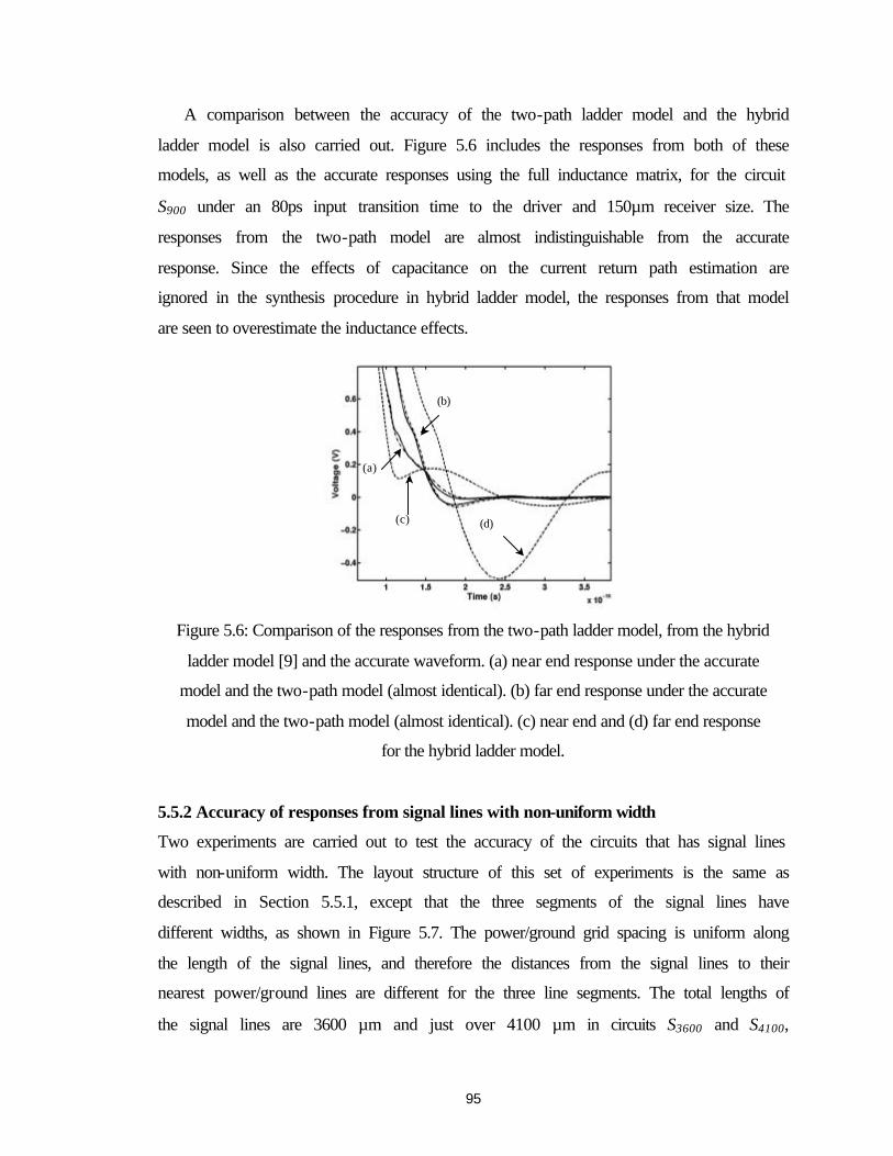
95
A comparison between the accuracy of the two-path ladder model and the hybrid
ladder model is also carried out. Figure 5.6 includes the responses from both of these
models, as well as the accurate responses using the full inductance matrix, for the circuit
S900 under an 80ps input transition time to the driver and 150µm receiver size. The
responses from the two-path model are almost indistinguishable from the accurate
response. Since the effects of capacitance on the current return path estimation are
ignored in the synthesis procedure in hybrid ladder model, the responses from that model
are seen to overestimate the inductance effects.
Figure 5.6: Comparison of the responses from the two-path ladder model, from the hybrid
ladder model [9] and the accurate waveform. (a) near end response under the accurate
model and the two-path model (almost identical). (b) far end response under the accurate
model and the two-path model (almost identical). (c) near end and (d) far end response
for the hybrid ladder model.
5.5.2 Accuracy of responses from signal lines with non-uniform width
Two experiments are carried out to test the accuracy of the circuits that has signal lines
with non-uniform width. The layout structure of this set of experiments is the same as
described in Section 5.5.1, except that the three segments of the signal lines have
different widths, as shown in Figure 5.7. The power/ground grid spacing is uniform along
the length of the signal lines, and therefore the distances from the signal lines to their
nearest power/ground lines are different for the three line segments. The total lengths of
the signal lines are 3600 µm and just over 4100 µm in circuits S3600 and S4100,
(a)
(b)
(c) (d)

96
respectively. The length of each segment in circuit S4100 is chosen to test the accuracy of
interpolation for the model parameters. Each of the three line segments is modeled by a
cascade of three two-path ladder model segments.
Figure 5.7: Top view of the structure of signal lines in circuits S3600 and S4100.
(W1/W2/W3=3.6/2.88/1.8µm, S3600: L1/L2/L3=1500/1200/900µm,
S4100: L1/L2/L3= 1670.4/1275/1194 µm, S=12µm)
Figure 5.8: The change of errors for overshoots in the range of transition times for circuit
S4100. Diamond: accurate overshoot with 30 µm receiver size. Square: accurate overshoot
with 330 µm receiver size. Triangle: approximate overshoot with 30 µm receiver size.
Cross: approximate overshoot with 330 µm receiver size.
For circuit S3600, the accumulated error from the series connection of model segments
with different width, length and spacing to power/ground grids are small, with 5% mean
error and 37% maximum error in timing characteristics and 26% maximum error and
20% mean error in the overshoot larger than 50 mV. In circuit S4100, the model
W1 W2 W3
L1 L2 L3
S Nearest power/ground lines
Dense power/ground mesh
0.00E+00
5.00E-02
1.00E-01
1.50E-01
2.00E-01
2.50E-01
1.00E-111.00E-101.00E-09
Transition times (s)
Ove
rsho
ot (
V)

97
parameters for the three line segments are obtained by interpolation. For example, the
model parameters for the segment with 1670.4 µm length can be interpolated from the
entries in the table corresponding to model parameters for two line segments that have the
same width and have the same supply network background as line segment 1, but have
lengths of 1500 µm and 1800 µm respectively. The accumulated errors caused by the
interpolation are small. The mean error in timing characteristics and overshoot are 7%
and 24% respectively. The errors of overshoot larger than 50 mV for circuit S4100 are
shown in Figure 5.8. The errors at high transition times are larger than those at low
transition times, but the maximum errors of 25% in overshoot is acceptable to the
requirements of most of the current on-chip noise analysis.
5.5.3 Accuracy of responses from a clock net
Three experiments are carried out to test the accuracy of three clock nets that have
multiple switching line segments with non-uniform width, non-uniform spacing to the
nearest power/ground grid lines and are on different metal layers. The layout region that
is considered in the simulation for the accurate responses includes one column of power
and ground pads on both sides of each switching line segments. Circuit CLKH, as shown
in Figure 5.9, is a clock H-tree with one source and sixteen sinks. There are 31 line
segments distributed on three metal layers M6, M7 and M8. The responses are measured
at the output of the source and the input of the sink at node C, while the sizes of the other
sinks are identical and are set to be 100 µm or 900 µm. The length of the path from the
source to sink at C is 3900 µm with five line segments that are modeled by fifteen model
segments are on this path. Circuit CLKHBF is an optimized version of circuit CLKH with
buffers inserted at all nodes marked D and E.

98
Figure 5.9: Top views of the structures of circuits CLKH. (A: driver input, B: driver
output, C: receiver input, D and E: buffer position in circuit CLKHBF.)
The maximum and mean errors of timing characteristics for circuit CLKH with 900
µm receiver sizes at all sinks except the one at C are 15% and 4%, while those for circuit
CLKHBF with the same sink sizes are 11% and 2% respectively. The overshoots in both
the circuits are smaller than 50 mV. It is reasonable that the errors for circuit CLKHBF are
smaller than those for circuit CLKH because the buffers are intended to reduce the
inductance effects and this also has the side effect of making the modeling easier and
more accurate.
Figure 5.10: Top view of the layout structure of a global clock net
(A: driver input, B: driver output, C: receiver input)
3.6mm
3.6mm
A
B
C
Global power/ground grid x
y
O
D
E
D
E
E E
6.6mm
5.9mm
A
B
C
Global power/ground grid x
y
O

99
The last and the largest circuit in the set of experiments is a clock net CLK whose
dimension is determined according to the layout shown in Figure 5.10. CLK has one
source and twelve sinks. There are 19 line segments distributed on two metal layers M7
and M8. The responses are measured at the output of the source and the input of the sink
at C, while the sizes of the other sinks are identical and are set to be 100 µm or 900 µm.
The length of the path from the source to sink at C is 3800 µm with five line segments
that are modeled by fifteen model segments are on this path. The model parameters for
each line segment are interpolated as was done in Section 5.5.2.
The maximum and mean errors of timing characteristics for circuit CLK with 900 µm
receiver sizes at all the sinks except node C are 21% and 5%. Figure 5.11 shows a set of
responses from the two-path ladder model and from the accurate responses under both
RC and RLC models for a typical circuit setup with a 90µm receiver size at node C,
270µm receiver size at the other sinks and a 100ps transition time at the driver input. The
responses at the near end are almost the same for the three simulations. The results from
the two-path ladder model match those of the accurate simulation well in terms of the
50% interconnect delay, the 50% gate delay, and the transition times at near and far ends.
Therefore, we have demonstrated that the proposed compact model can be used to replace
complicated layout structures to rapidly estimate their responses.
Figure 5.11: Comparison of the responses from the two-path ladder model and the
accurate responses. (a) near ends in RC, RLC and two-path model.
(b)-(d) far ends in RC, RLC and two-path model.
(a)
(b)
(c)
(d)

100
5.6 Conclusion
A two-path ladder model for compact modeling of on-chip interconnect timing and noise
analysis is proposed in this work to accurately approximate the proximity effect in high
speed circuits. The synthesis procedure uses constrained nonlinear optimization to match
the response characteristics of the model to those under an accurate simulation, which are
calculated using a comprehensive PEEC model and include the effects of capacitances on
the current return path estimation. A comparison with the hybrid ladder modeling shows
that the proposed modeling in this work results in more accurate responses.

101
Chapter 6
Conclusion
This thesis work develops three algorithms, corresponding to simulation, extraction and
modeling of on-chip inductance issues.
A precorrected-FFT algorithm for fast and accurate simulation of inductive systems is
proposed, in which long-range components of the magnetic vector potential are
approximated by grid currents, while nearby interactions are calculated directly. All
inductance interactions are considered in computing the product of the inductance matrix
with a given vector, so that the waveforms at the nodes of interest are calculated
accurately. A comparison with the block diagonal algorithm showed that the
precorrected-FFT method results in more accurate waveforms and less run time with
much smaller memory consumption. Different approximations in the precorrected-FFT
method, including using a two-dimensional grid structure, were tested and showed that
the lower order of approximation greatly increases the speed and reduces the memory
consumption without much loss in accuracy. Experiments carried out on large industrial
circuits demonstrate that the precorrected-FFT method is a fast and highly accurate
approach for on-chip inductance simulation in large circuits.

102
Two circuit-aware based sparsification methodologies for fully coupled PEEC K-
element representations for an inductive system are proposed by analyzing the circuit
characteristics and clustering the inductances according to their relative importance to the
circuit. In both algorithms, all of the switching lines are classified as ID or RD lines.
Strong couplings are resolved first and weak couplings are then added to the clusters.
Algorithm 2 works with the assumption of zero ∑j
jij dtdIL )/( drop on the supply lines
while Algorithm 1 has no such limitation. The experimental results in this work show the
effectiveness of the circuit-aware method compared with the shift-and-truncate method.
Algorithm 2 works well in a good design where supply lines behave more perfectly and
often gives a high sparsification but a relatively low accuracy. Algorithm 1 is designed
for any circuit and provides a high accuracy but with a lower sparsification than that of
Algorithm 2. The circuit-aware method helps to determine current return paths for a
design and identifies the most critical inductance terms for optimization.
A two-path ladder model for compact modeling of on-chip interconnect timing and
noise analysis is proposed to accurately approximate the proximity effect in high speed
circuits. The paths for both the high and low frequency currents are explicitly included in
the model. The synthesis procedure uses constrained nonlinear optimization to match the
response characteristics of the model to those under an accurate simulation, which are
calculated using a comprehensive PEEC model and include the effects of capacitances on
the current return path estimation. A comparison with the hybrid ladder modeling shows
that the proposed modeling in this work results in more accurate responses. Extensive
experiments are carried out on single signal lines and clock nets to test the accuracy of
the two-path ladder model. Experiments on several circuits demonstrate that the proposed
table look-up based compact modeling is a highly accurate and fast approach for on-chip
interconnect timing and noise analysis in large circuits. The compact modeling in this
work is especially suitable for single switching lines. The future work aims at developing
compact models for circuits with multiple switching lines.

103
Bibliography
[1] The International Technology Roadmap for Semiconductors. Available at
http://public.itrs.net/Files/2001ITRS/Home.html: Semiconductor Industry
Association, 2001.
[2] G. E. Moore, “Cramming More Components onto Integrated Circuits,” Electronics
Magazine, pp. 114-117, vol. 38, April 1965.
[3] Y. Massoud and Y. Ismail, “Gasping the Impact of On-Chip Inductance,” IEEE
Circuits & Devices Magazine, vol. 17, No. 4, pp. 14-21, July 2001.
[4] F. C. Li, J. C. Keh and R. Mathews, “Simulating Frequency-Dependent Current
Distribution for Inductance Modeling of On-Chip Copper Interconnects,” Proc. of the
International Symposium on Physical Design, pp. 117-120, April 2000.
[5] Y. I. Ismail, E. G. Friedman and J. L. Neves, “Exploiting On-Chip Inductance in High
Speed Clock Distribution Networks,” IEEE Workshop on Signal Processing Systems.
pp. 643-652, 2000.
[6] A. Deutsch, G. V. Kopcsay, P. J. Restle, H. H. Smith, G. Katopis, W. D. Becker, P.
W. Coteus, C. W. Surovic, B. J. Rubin, R. P. Dunne, T. Gallo, K. A. Jenkins, L. M.
Terman, R. H. Dennard, G. A. Sai-Halasz, B. L. Krauter and D. R. Knebel, “When
are Transmission Line Effects Important for On-Chip Interconnections?” IEEE
Transactions on Microwave Theory & Techniques, vol. 45, No. 10, pp. 1836-46,
October 1997.

104
[7] Y. I. Ismail, E. G. Friedman and J. L. Neves, “Figures of Merit to Characterize the
Importance of On-Chip Inductance,” Proc. of the ACM/IEEE Design Automation
Conference, pp.560-565, June 1998.
[8] A. E. Ruehli, “Inductance Calculations in a Complex Integrated Circuit
Environment,” IBM Journal of Research and Development, pp. 470-481, vol. 16, No.
5, September 1972.
[9] E. Rosa, “The Self and Mutual Inductance of Linear Conductors,” Bulletin of the
National Bureau of Standards, pp 301-344, 1908.
[10] A. E. Ruehli, “Equivalent Circuit Models for Three-Dimensional Multiconductor
Systems,” IEEE Transactions on Microwave Theory & Techniques, vol. MTT-22,
No.3, pp.216-221, March 1974.
[11] P. J. Restle, A. E. Ruehli, S. G. Walker and G. Papadopoulos, “Full-Wave PEEC
Time-Domain Method for the Modeling of On-Chip Interconnects,” IEEE
Transactions on Computer-Aided Design of Integrated Circuits & Systems, vol. 20,
No. 7, pp. 877-886, July 2001.
[12] Z. He, M. Celik and L. T. Pileggi, “SPIE: Sparse Partial Inductance Extraction,”
Proc. of the ACM/IEEE Design Automation Conference, pp. 137-140, June 1997.
[13] B. Krauter and L. T. Pileggi, “Generating Sparse Inductance Matrices with
Guaranteed Stability,” Proc. of the IEEE/ACM International Conference on
Computer-Aided Design, pp. 45-52, November 1995.
[14] M. Beattie, B. Krauter, L. Alatan and L. Pileggi, “Equipotential Shells for Efficient
Inductance Extraction,” IEEE Transactions on Computer-Aided Design of Integrated
Circuits & Systems, pp. 70-79, vol. 20, No. 1, January 2001.
[15] A. J. Dammers and N. P. Van Der Meijs, “Virtual Screening: A Step Towards a
Sparse Partial Inductance Matrix,” Proc. of the IEEE/ACM International Conference
on Computer-Aided Design, pp. 445-452, November 1999.
[16] K. Gala, D. Blaauw, J. Wang, M. Zhao and V. Zolotov, “Inductance 101: Analysis
and Design,” Proc. of the ACM/IEEE Design Automation Conference, pp. 329-334,
June 2001.

105
[17] A. Devgan, H. Ji and W. Dai, “How to Efficiently Capture On-Chip Inductance
Effects: Introducing a New Circuit Element K,” Proc. of the IEEE/ACM International
Conference on Computer-Aided Design, pp. 150-155, November 2000.
[18] H. Ji, A. Devgan and W. Dai, “KSPICE: Efficient and Stable RKC Simulation for
Capturing On-Chip Inductance Effect,” Technical Report UCSC-CRL-00-10,
University of California Santa Cruz, Santa Cruz, CA, 2000. Available at
http://ftp.cse.ucsc.edu/pub/tr/ucsc-csl-00-10.ps.Z.
[19] A. Odabasioglu, M. Celik and L. T. Pileggi, “PRIMA: Passive Reduced-Order
Interconnect Macromodeling Algorithm,” Proc. of the IEEE/ACM International
Conference on Computer-Aided Design, pp. 58-65, November 1997.
[20] M. Beattie and L. Pileggi, “IC Analyses Including Extracted Inductance Models,”
Proc. of the ACM/IEEE Design Automation Conference, pp.915-920, June 1999.
[21] B. Krauter, S. Mehrotra and V. Chandramouli, “Including Inductance Effects in
Interconnect Timing Analysis,” Proc. of the IEEE Custom Integrated Circuits
Conference, pp 445-452, May 1999.
[22] M. Beattie, S. Gupta and L. Pileggi, “Hierarchical Interconnect Circuit Models,”
Proc. of the IEEE/ACM International Conference on Computer-Aided Design, pp.
215-221, November 2000.
[23] K. L. Shepard and Z. Tan, “Return-Limited Inductances: A Practical Approach to
On-Chip Inductance Extraction,” Proc. of the IEEE Custom Integrated Circuits
Conference, pp. 453-456, May 1999.
[24] M. Kamon, M. J. Tsuk and J. White, “FastHenry: A Multipole-Accelerated 3-D
Inductance Extraction Program,” Proc. of the ACM/IEEE Design Automation
Conference, pp. 678-683, June 1993.
[25] A. Sinha and S. Chowdhury, “Mesh-Structured On-Chip Power/Ground Design for
Minimum Inductance and Characterization for Fast R, L Extraction,” Proc. of the
IEEE Custom Integrated Circuits Conference, pp 461-464, May 1999.
[26] S. Lin, N. Chang and S. Nakagama, “Quick On-Chip Self- and Mutual-Inductance
Screen,” Proc. of the International Symposium on Quality in Electronic Design, pp.
513-520, March 2000.

106
[27] X. N. Qi, G. F. Wang, Z. P. Yu, R. W. Dutton, Y. Tak and N. Chang, “On-Chip
Inductance Modeling and RLC Extraction of VLSI Interconnects for Circuit
Simulation,” Proc. of the IEEE Custom Integrated Circuits Conference, pp. 487-90,
May 2000.
[28] C. C. Huang and J. H. Chern, “Accurate Modeling of Capacitive, Resistive and
Inductive Effects of Interconnect,” IEEE WESCON/95 Conference Record, pp. 115-
117, 1995.
[29] L. He, N. Chang, S. Lin and O. S. Nakagama, “An Efficient Inductance Modeling
for On-Chip Interconnects,” Proc. of the IEEE Custom Integrated Circuits
Conference, pp. 457-460, May 1999.
[30] Y. C. Lu, K. Banerjee, M. Celik and R. W. Dutton, “A Fast Analytical Technique for
Estimating the Bounds of On-Chip Clock Wire Inductance,” Proc. of the IEEE
Custom Integrated Circuits Conference, pp. 241 - 244, May 2001.
[31] K. Banerjee and A. Mehrotra, “Analysis of On-Chip Inductance Effects Using a
Novel Performance Optimization Methodology for Distributed RLC Interconnects,”
Proc. of the ACM/IEEE Design Automation Conference, pp. 137-140, June 2001.
[32] Y. I. Ismail, E. G. Friedman, and J. L. Neves, "Repeater Insertion in Tree Structured
Inductive Interconnect," IEEE Transactions on Circuits and Systems II: Analog and
Digital Signal Processing, pp. 471-481, vol. 48, No. 5, May 2001.
[33] S. C. Chan and K. L. Shepard, “Practical Consideration in RLCK Crosstalk Analysis
for Digital Integrated Circuits,” Proc. of the IEEE/ACM International Conference on
Computer-Aided Design, pp. 598-604, November 2001.
[34] L. He and K. M. Lepak, “Simultaneous Shield Insertion and Net Ordering for
Capacitive and Inductive Coupling Minimization,” Proc. of International Symposium
on Physical Design, pp. 55-60, April 2000.
[35] G. Zhong, C-K. Koh and K. Roy, “A Twisted-Bundle Layout Structure for
Minimizing Inductive Coupling Noise,” Proc. of the IEEE/ACM International
Conference on Computer-Aided Design, pp. 406-411, November 2000.
[36] Y. Massoud, S. Majors, T. Bustami and J. White, “Layout Techniques for
Minimizing On-Chip Interconnect Self-Inductance,” Proc. of the ACM/IEEE Design
Automation Conference, pp.566-571, June 1998.

107
[37] H. Hu and S. Sapatnekar, “Circuit-Aware On-chip Inductance Extraction,” Proc. of
the IEEE Custom Integrated Circuits Conference, pp. 245 - 248, May 2001.
[38] B. Krauter and S. Mehrotra, “Layout Based Frequency Dependent Inductance and
Resistance Extraction for On-chip Interconnect Timing Analysis,” Proc. of the
ACM/IEEE Design Automation Conference, pp. 303-308, June 1998.
[39] H. A. Wheeler, “Formulas for the Skin-Effect,” Proc. of the Institute of Radio
Engineers, pp. 412-424, vol. 30, September 1942.
[40] W. Press, S. Teukolsky, W. T. Vetterling and B. P. Flannery, Numerical Recipes in
C, Cambridge University Press, NY, 1992.
[41] J. R. Philips and J. K. White, “A Precorrected-FFT Method for Capacitance
Extraction of Complicated 3-D Structures,” Proc. of the IEEE/ACM International
Conference on Computer-Aided Design, pp. 268-271, November 1994.
[42] J. R. Philips and J. K. White, “A Precorrected-FFT Method for Electrostatic
Analysis of Complicated 3-D Structures,” IEEE Transactions on Computer-Aided
Design of Integrated Circuits & Systems, pp.1059-1072, vol.16, No.10, October 1997.
[43] J. Lillis, C. K. Cheng, S. Lin and N. Chang, High-Performance Interconnect
Analysis and Synthesis, John Wiley, NY, 1999.
[44] D. Luenberfger, Linear and Non-Linear Programming, Addison-Wesley, NY, 1989.
[45] H. Hu and S. S. Sapatnekar, “Efficient Inductance Extraction using Circuit-Aware
Techniques,” accepted by the IEEE Transactions on Very Large Scale Integration
Systems.
[46] H. Hu and S. S. Sapatnekar, “Efficient PEEC-based Inductance Extraction using
Circuit-Aware Techniques,” submitted to the IEEE/ACM International Conference on
Computer Design, 2002.
[47] H. Hu, D. T. Blaauw, V. Zolotov, K. Gala, M. Zhao, R. Panda and S. S. Sapatnekar,
“A Precorrected-FFT Method for Simulating On-chip Inductance,” submitted to the
IEEE/ACM International Conference on Computer Aided Design, 2002.
[48] H. Hu, D. T. Blaauw, V. Zolotov, K. Gala, M. Zhao, R. Panda and S. S. Sapatnekar,
“Fast On-chip Inductance Simulation using a Precorrected-FFT Method,” submitted
to the IEEE Transactions on Computer-Aided Design of Integrated Circuits and
Systems.

108
[49] H. Hu, D. T. Blaauw, V. Zolotov, R. Panda and S. S. Sapatnekar, “Table Look-up
Based Compact Modeling for On-chip Interconnect Timing and Noise Analysis,”
submitted to the IEEE/ACM International Conference on Computer Aided Design,
2002.
[50] C. Hoer and C. Love, “Exact Inductance Equations for Rectangular Conductors with
Applications to More Complicated Geometries,” J. Res. Nat. Bureau of Standards,
pp. 127-137, vol. 69C, No. 2, April-June 1965.
[51] F. W. Grover, Inductance calculations: Working Formulas and Tables, Dover
Publications, New York, NY, 1946.
[52] A. J. Sinclair and J. A. Ferreira, “Analysis and Design of Transmission-Line
Structures by means of the Geometric Mean Distance,” IEEE AFRICON, Electrical
Energy Technology, Communication Systems, Human Resources, pp. 1062-1065,
September 1996.
[53] N. Delorme, M. Belleville and J. Chilo, “Inductance and Capactance Analytic
Formulas for VILI Interconnects,” IEEE Electronics Letters, EDL-32, pp 996-997,
1996.
[54] N. Delorme, M. Belleville and J. Chilo, “Inductance and Capacitance Analytic
Formulas for VLSI Interconnects,” Electronics Letters, vol. 32, No. 11, pp. 996-7,
May 1996.
[55] J. H. Chern, J. Huang, L. Arledge, P-C Li and P. Yang, “Multilevel Metal
Capacitance Models for CAD Design Synthesis Systems,” IEEE Electron Device
Letters, vol. 13, No. 1, pp. 32-34, January 1992.
[56] D. J. Griffiths, Introduction to Electrodynamics. 2nd edition, Prentice Hall,
Englewood Cliffs, NJ, 1989.
[57] G. W. Stewart, Introduction to Matrix Computations. Academic Press, New York,
NY, 1973.
[58] K. Nabors, F. T. Korsmeyer, F. T. Leighton and J. K. White, “Precorrection,
Adaptive, Multipole-Accerelated Interactive Methods for Three-Dimensional
Potential Integral Equations of the First Kind,” Available at http://rle-
vlsi.mit.edu/~white/pubs/siammulti.ps

109
[59] I. S. Gradshteyn and I. M. Ryzhik, Table of Integrals, Series and Products,
Academic Press, NY, 2000.
[60] J. Cong, “Challenges and Opportunities for Design Innovations in Nanometer
Technologies,” SRC Design Science Concept Paper, 1997. Available at
http://cadlab.cs.ucla.edu/~cong/papers/src_report97_final.ps
[61] K. Gala, V. Zolotov, R. Panda, B. Young, J. Wang and D. Blaauw, “On-chip
Inductance Modeling and Analysis,” Proc. of the ACM/IEEE Design Automation
Conference, pp.63-68, June 2000.
[62] A. E. Ruehli, Circuit Analysis, Simulation and Design, vol. 3, Part 2, North-Holland,
Amsterdam, The Netherlands, 1987.