University of Groningen Strain and composition effects in ...
29
University of Groningen Strain and composition effects in epitaxial ferroelectrics Rispens, Gijsbert IMPORTANT NOTE: You are advised to consult the publisher's version (publisher's PDF) if you wish to cite from it. Please check the document version below. Document Version Publisher's PDF, also known as Version of record Publication date: 2010 Link to publication in University of Groningen/UMCG research database Citation for published version (APA): Rispens, G. (2010). Strain and composition effects in epitaxial ferroelectrics: structural studies on PbxSr1- xTiO3 thin films grown by MBE. s.n. Copyright Other than for strictly personal use, it is not permitted to download or to forward/distribute the text or part of it without the consent of the author(s) and/or copyright holder(s), unless the work is under an open content license (like Creative Commons). The publication may also be distributed here under the terms of Article 25fa of the Dutch Copyright Act, indicated by the “Taverne” license. More information can be found on the University of Groningen website: https://www.rug.nl/library/open-access/self-archiving-pure/taverne- amendment. Take-down policy If you believe that this document breaches copyright please contact us providing details, and we will remove access to the work immediately and investigate your claim. Downloaded from the University of Groningen/UMCG research database (Pure): http://www.rug.nl/research/portal. For technical reasons the number of authors shown on this cover page is limited to 10 maximum. Download date: 24-03-2022
Transcript of University of Groningen Strain and composition effects in ...

University of Groningen
Strain and composition effects in epitaxial ferroelectricsRispens, Gijsbert
IMPORTANT NOTE: You are advised to consult the publisher's version (publisher's PDF) if you wish to cite fromit. Please check the document version below.
Document VersionPublisher's PDF, also known as Version of record
Publication date:2010
Link to publication in University of Groningen/UMCG research database
Citation for published version (APA):Rispens, G. (2010). Strain and composition effects in epitaxial ferroelectrics: structural studies on PbxSr1-xTiO3 thin films grown by MBE. s.n.
CopyrightOther than for strictly personal use, it is not permitted to download or to forward/distribute the text or part of it without the consent of theauthor(s) and/or copyright holder(s), unless the work is under an open content license (like Creative Commons).
The publication may also be distributed here under the terms of Article 25fa of the Dutch Copyright Act, indicated by the “Taverne” license.More information can be found on the University of Groningen website: https://www.rug.nl/library/open-access/self-archiving-pure/taverne-amendment.
Take-down policyIf you believe that this document breaches copyright please contact us providing details, and we will remove access to the work immediatelyand investigate your claim.
Downloaded from the University of Groningen/UMCG research database (Pure): http://www.rug.nl/research/portal. For technical reasons thenumber of authors shown on this cover page is limited to 10 maximum.
Download date: 24-03-2022

Chapter 3
X-Ray diffraction as a tool for
characterization of ferroelectrics
3.1 Introduction
X-ray diffraction (XRD) is a widely used technique to determine crystal structures.
Applied to thin films, XRD is most typically used to determine the lattice param-
eters and thickness. However, much more information can be obtained from XRD
experiments. In this chapter we will show how XRD can be give information about
the properties and domain structure of ferroelectric thin films.
In the first half of the chapter, the basics of X-ray diffraction and the various
measurement geometries are described. In the second half of the chapter, the char-
acterization of ferroelectrics by XRD is described. The relation between the lattice
parameters and polarization is discussed in section 3.4. This relation was used to
determine the transition temperature in PbxSr1−xTiO3 thin films (chapter 4). Sec-
tion 3.5 shows the wealth of information that can be obtained from simulation of
the crystal truncation rods of ferroelectric thin films, such as the direction of the
polarization.
Periodic ferroelectric domains can give rise to a XRD superstructure if the pe-
riodicity has a sufficiently large coherence length. In section 3.6 we will show ex-
amples of such periodic structures and show how modeling of these patterns can
41
42 X-Ray diffraction as a tool for characterization of ferroelectrics
be employed to determine the the orientation of the polarization and the domain
walls. The examples will show that careful analysis of XRD diffraction data can
give much more information that just the lattice parameters and thickness of ferro-
electric thin films.
3.2 Theory
3.2.1 X-Ray diffraction
X-rays are scattered by electrons. This scattering is at the basis of x-ray diffraction.
In a crystal the electrons density peaks at the atomic positions. X-rays scattered
from this periodic lattice of electron density interfere to give a diffraction pattern.
The theory of x-ray diffraction reflects this description. [90,91] The starting point is
the scattering of x-rays from an electron. The amplitude of scattered wave is
A1 = A0e2
mc21R
e[i(k f −ki)re] (3.1)
where A0 is the amplitude of the incident wave, R is the distance from the elec-
tron position re. ki and k f are the incident and scattered wave vectors, respectively.
e2/mc2 (≈ 2.82×10⁻⁵ A) is the Thomson scattering length, or alternatively the clas-
sical radius of the electron. The small value of the Thomson scattering length is the
reason why the interaction between x-rays and matter is weak.
The atomic form factor is defined as the Fourier transform of the electron den-
sity of the atom (ρ)
f 0(q) =∫ρ(r)eiq·rdr (3.2)
where q = k f - ki is the momentum transfer or scattering vector. In the case of
elastic scattering∣∣k f∣∣ = |ki| = 2π/λ. Because of the different energy level of
different electrons not all will follow the x-rays in the same way. The response of
the more tightly bound electrons is reduced, and the phase is changed with respect
to that of the outer shell electrons. These effects are taken into account by adding
f ′ and f ′′ in the atomic form factor, the so-called dispersion corrections.
f (q, hω) = f 0(q) + f ′(hω) + i f ′′(hω) (3.3)
3.2 Theory 43
Analytical expansions of f 0(Q) and the dispersion corrections for various x-ray
energies can be found the International Tables for Crystallography [92].
Once the atomic form factors are known, the scattering amplitude of a crystal is
found by summing all atoms in the crystal with the correct phases, because a crystal
can be described by a unit cell that is translated into three dimensions. This transla-
tional symmetry is used to separate the scattering amplitude into two factors: The
structure factor and the lattice sum, as follows
A(q) = −r0 ∑r j
f j(q)eiq·r j ∑Rn
eiq·Rn (3.4)
The first factor, the unit cell structure factor, sums all atoms in the unit cell, where
r j is the position of atom j. The second factor, sums over the entire crystal, where
Rn is the position of unit cell n. A primitive perovskite unit cell consists of 5 atoms
and thus the structure factor can be evaluated explicitly. In a bulk crystal the lattice
sum runs to infinity in all three directions. When the lattice sum is then evaluated
this gives rise to a delta function that peaks when q = G, where G is a reciprocal
lattice point. q = G is called the Laue condition for diffraction. It can be shown that
this condition is equivalent to the well known Bragg’s law. The reciprocal vectors
are expressed as
G = ha∗1 + ka∗2 + la∗3 (3.5)
where h, k, l are integers called Miller indices and a∗i are the reciprocal lattice pa-
rameters
a∗1 =2πvc
a∗2 × a∗3 a∗2 =2πvc
a∗3 × a∗1 a∗3 =2πvc
a∗1 × a∗2 (3.6)
where vc = a1 · a2 × a3 is the unit cell volume. To obtain the diffracted intensity, the
scattering amplitude has to be multiplied by its complex conjugate. The lattice sum
determines the position of the diffraction peaks and the structure factor determines
the intensity and the presence of possible systematic absences.
When studying thin films, evaluating the lattice sums by assuming an infinite
lattice in three directions is not valid. A thin film can be considered as being infinite
in two directions, while the third direction consists of a finite number of unit cells.

44 X-Ray diffraction as a tool for characterization of ferroelectrics
Evaluating the lattice sum in the a3 direction for a finite number of monolayers (N)
givesN−1
∑n=0
eiqza3n =1 − eiqza3 N
1 − eiqza3(3.7)
where the following result for geometric series has been used
N−1
∑n=0
kn =1 − kN
1 − k(3.8)
with |k| < 1. Where the diffraction condition is fulfilled eiqza3 = 1, and thus, the
intensity will go to infinity. This divergence does not occur when the absorption of
x-rays is included [93]. The lattice sum then becomes
N−1
∑n=0
e(iqza3+ε)n =1 − e(iqza3+ε)N
1 − eiqza3+ε(3.9)
whereε is the absorption coefficient. This expression for the lattice sum can be used
to calculate the scattering amplitude and the intensity. Figure 3.1a shows the cal-
culated intensity around the (001) Bragg reflection of a PbTiO3 slab 25 monolayers
thick. Both the width of the central peak and the period of the fringes are a measure
of the film thickness.
For the substrate the lattice sum runs from 0 to infinity and expression 3.9 be-
comes−∞
∑n=0
e(iqza3+ε)n =1
1 − eiqza3+ε(3.10)
The intensity calculated using this lattice sum still shows a sharp peak, but in con-
trast to a delta function, there is intensity in between the peaks, as shown in figure
3.1b.
To construct a crystal that consists of a substrate with a thin film on top, both the
film and substrate scattering factors are added. Both the lattice sum of the substrate
and the film start at 0 and thus a phase factor corresponding to the film thickness
has to be added to the substrate contribution
A(qz) = −ao
(FPbTiO3
1 − e(iqza3+ε)N
1 − eiqza3+ε+[
FSrTiO3
11 − eiqza3+ε
]eiqza3N
)(3.11)

3.2 Theory 45
0.16 0.18 0.2 0.2210
1
102
103
104
105
106
K [2k0]
Inte
nsity
(a.u
.)
0.16 0.18 0.2 0.2210
1
102
103
104
105
106
K [2k0]
Inte
nsity
(a.u
.)
0.16 0.18 0.2 0.22
102
104
106
K [2k0]
Inte
nsity
(a.u
.)
a) b)
c)
Figure 3.1: a) Calculated intensity for a TiO2 terminated PbTiO3 slab of 25 monolayersthick (3.9). b) Calculated intensity for a TiO2 terminated SrTiO3 substrate (3.10). Calculatedintensity for a TiO2 terminated SrTiO3 substrate with a 25 monolayer PbTiO3 thin film ontop (3.11). The horizontal axes are in units of 2k0, where k0 = 2π
λ
where FPbTiO3 and FSrTiO3 are the structure factors of PbTiO3 and SrTiO3 respec-
tively. Expression (3.11) can be used to simulate experimental out-of-plane diffrac-
tion results, that is 2θ-ω scans. A plot of the calculated intensity for a 25 monolayer
thick PbTiO3 film on a SrTiO3 substrate is shown in figure 3.1c.
3.2.2 X-Ray reflectivity
A related, but different, technique to study thin films using x-rays is x-ray reflectiv-
ity. X-ray reflectivity can give information about the electron density, thickness and
roughness of a thin film. The main difference between reflectivity and diffraction is
46 X-Ray diffraction as a tool for characterization of ferroelectrics
that reflectivity does not require a well ordered crystal structure, thus amorphous
materials can also be studied. The basis of reflectivity is the interference between
x-rays that are refracted and reflected at interfaces between layers with different
electron density.
The theory of reflectivity is based on the theory of refraction in optics. The main
difference between refraction at optical wavelengths and for x-rays is that the index
of refraction for x-rays is very small and smaller than unity. The refractive index
for x-rays can be expressed in terms of the atomic form factor (equation 3.3) as
n ≡ 1 − 2πρar0
k2
(f 0(0) + f ′ + i f ′′
)(3.12)
where ρa is the atomic density, f0(0) the number of electrons in the atom, r0 the
Thomson scattering length and k is 2π/λ. Snell’s law relates the refracted angle α j
to the incident angleαi:
cosαi = n cosα j (3.13)
The refractive index of the layer and the substrate can be calculated using knowl-
edge of the materials such as atomic constituents and unit cell volumes.
As the index of refraction for x-rays is smaller than unity, total reflection oc-
curs below some critical angle αc, where α j ≤ 0. At these small angles, a Taylor
expansion of the cosine gives a relation for the critical angle:
αc =√
4πρar0
k2 ( f 0(0) + f ′) (3.14)
where ρa f 0(0) is the electron density of the material. The critical angle is then a
measure of the electron density and can be used to determine the stoichiometry
of the material. In the case of PbTiO3, the critical angle is specially sensitive to
Pb vacancies as the contribution of Pb to the electron density is by far the largest.
Below the critical angle the reflectivity is almost 100%, and a part of the x-rays
penetrates the material as an evanescent wave, which has a penetration depth of
≈10 A, propagating parallel to the surface. The evanescent wave can be used to
measure in-plane Bragg peaks, avoiding the substrate signal. This technique is
called Grazing Incidence Diffraction (GID).
3.2 Theory 47
0 2 4 6 8 10100
102
104
106
2θ(o)
Inte
nsity
(a.u
.)
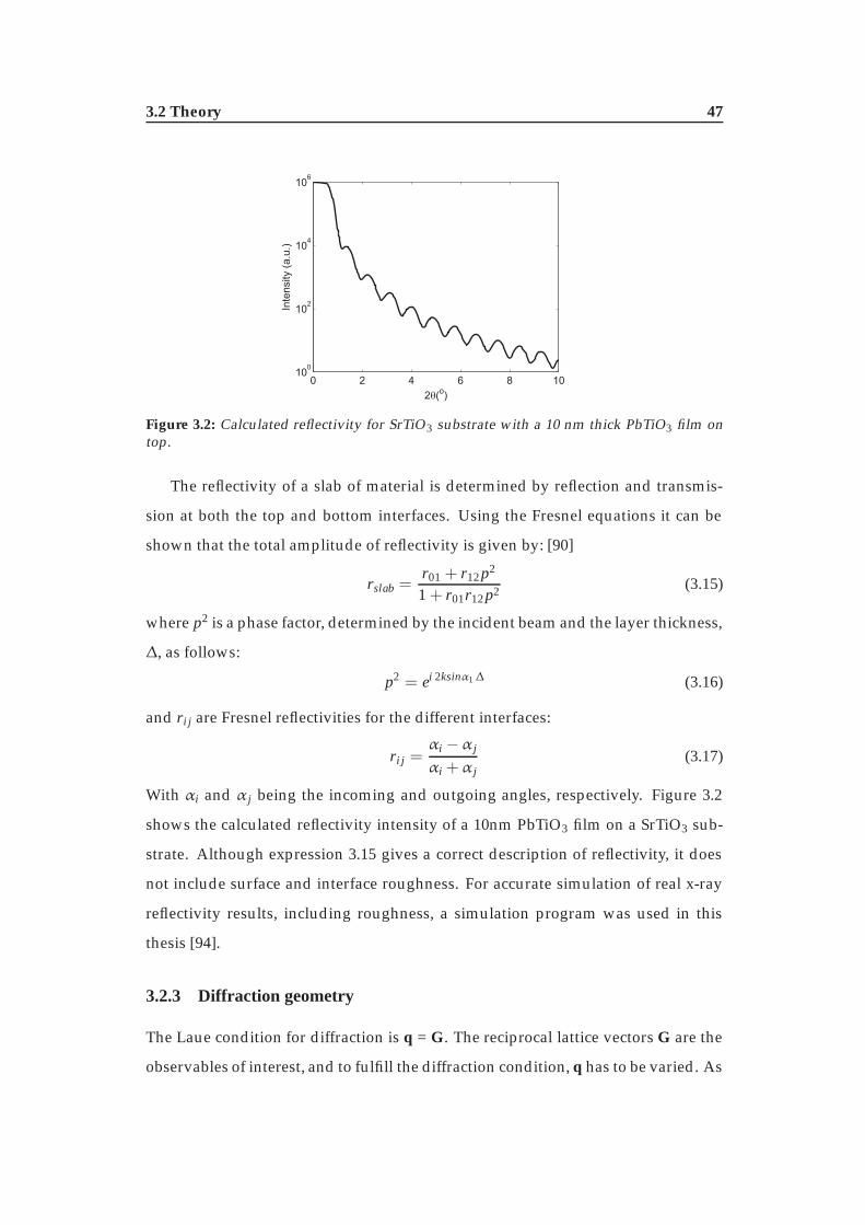
Figure 3.2: Calculated reflectivity for SrTiO3 substrate with a 10 nm thick PbTiO3 film ontop.
The reflectivity of a slab of material is determined by reflection and transmis-
sion at both the top and bottom interfaces. Using the Fresnel equations it can be
shown that the total amplitude of reflectivity is given by: [90]
rslab =r01 + r12p2
1 + r01r12p2 (3.15)
where p2 is a phase factor, determined by the incident beam and the layer thickness,
Δ, as follows:
p2 = ei 2ksinα1 Δ (3.16)
and ri j are Fresnel reflectivities for the different interfaces:
ri j =αi −α j
αi +α j(3.17)
With αi and α j being the incoming and outgoing angles, respectively. Figure 3.2
shows the calculated reflectivity intensity of a 10nm PbTiO3 film on a SrTiO3 sub-
strate. Although expression 3.15 gives a correct description of reflectivity, it does
not include surface and interface roughness. For accurate simulation of real x-ray
reflectivity results, including roughness, a simulation program was used in this
thesis [94].
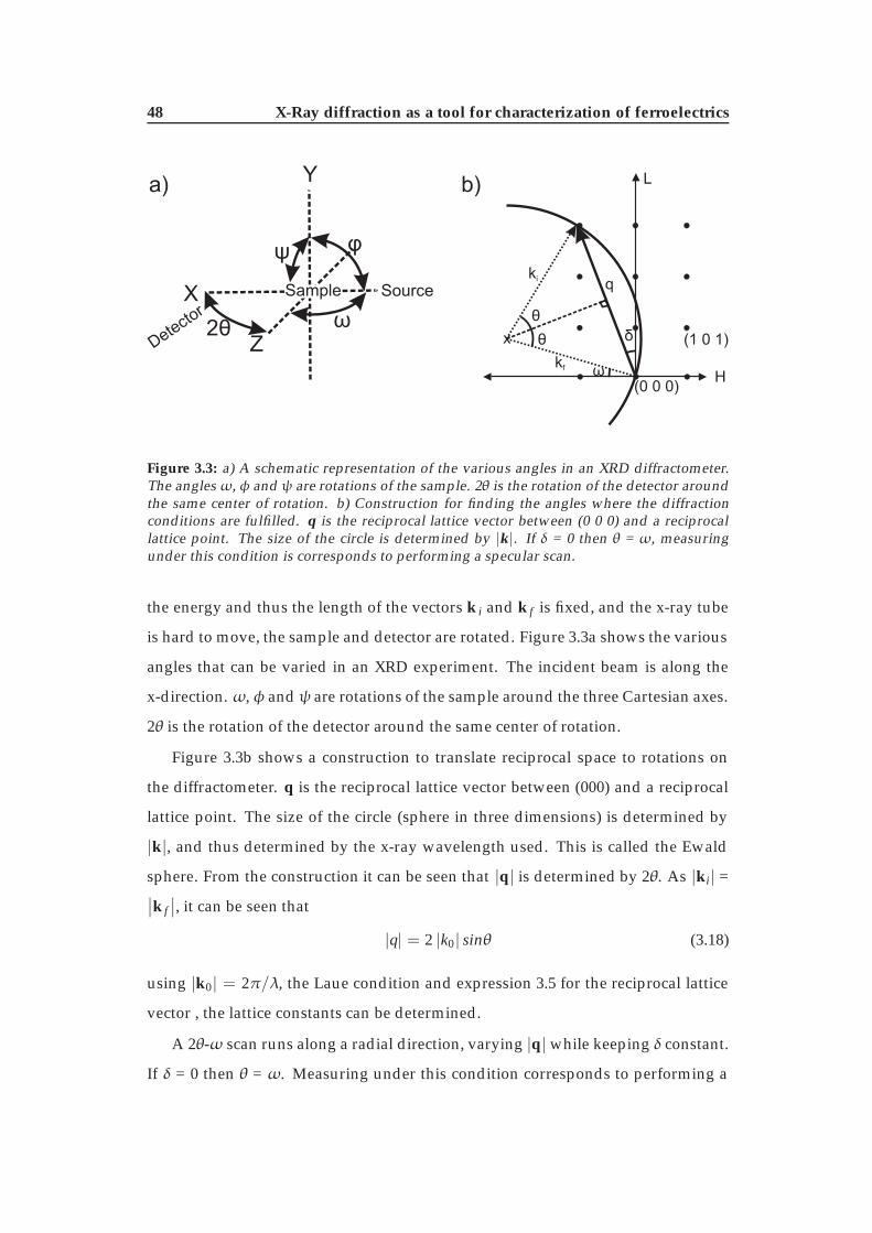
3.2.3 Diffraction geometry
The Laue condition for diffraction is q = G. The reciprocal lattice vectors G are the
observables of interest, and to fulfill the diffraction condition, q has to be varied. As
48 X-Ray diffraction as a tool for characterization of ferroelectrics
Y
X
Z2θ
ψ
ω
φ
Source
Detecto
r
Sample
a) b)
H
L
θ
ωkf
ki
δ
q
x
(0 0 0)
(1 0 1)θ
Figure 3.3: a) A schematic representation of the various angles in an XRD diffractometer.The anglesω,φ andψ are rotations of the sample. 2θ is the rotation of the detector aroundthe same center of rotation. b) Construction for finding the angles where the diffractionconditions are fulfilled. q is the reciprocal lattice vector between (0 0 0) and a reciprocallattice point. The size of the circle is determined by |k|. If δ = 0 then θ = ω, measuringunder this condition is corresponds to performing a specular scan.
the energy and thus the length of the vectors k i and k f is fixed, and the x-ray tube
is hard to move, the sample and detector are rotated. Figure 3.3a shows the various
angles that can be varied in an XRD experiment. The incident beam is along the
x-direction. ω,φ andψ are rotations of the sample around the three Cartesian axes.
2θ is the rotation of the detector around the same center of rotation.
Figure 3.3b shows a construction to translate reciprocal space to rotations on
the diffractometer. q is the reciprocal lattice vector between (000) and a reciprocal
lattice point. The size of the circle (sphere in three dimensions) is determined by
|k|, and thus determined by the x-ray wavelength used. This is called the Ewald
sphere. From the construction it can be seen that |q| is determined by 2θ. As |ki| =∣∣k f∣∣, it can be seen that
|q| = 2 |k0| sinθ (3.18)
using |k0| = 2π/λ, the Laue condition and expression 3.5 for the reciprocal lattice
vector , the lattice constants can be determined.
A 2θ-ω scan runs along a radial direction, varying |q| while keeping δ constant.
If δ = 0 then θ = ω. Measuring under this condition corresponds to performing a
3.2 Theory 49
specular scan. The calculated diffraction pattern shown in figure 3.1c is an exam-
ple of such a specular scan. A specular scan runs along the out-of-plane direction
in reciprocal space, without an in-plane component. The specular 2θ-ω is the de-
fault scan for determining the out-of-plane lattice constants and identification of
impurity phases.
To probe reciprocal lattice points with an in-plane component, an offset δ has
to be applied, by which ω �= θ. Such scans are useful in order to find the in-
plane lattice parameters and the relation between film and substrate. Reciprocal
space maps (RSM) around an off-specular reflection can show whether the film and
substrate are coherent, whether they have the same in-plane lattice parameter. A
RSM consists of a series of 2θ-ω scans with different offsets. As the relation between
the diffraction peaks is hard to determine from a 2θ-ω versus δ map directly, it is
useful to transform the angles to reciprocal space coordinates.
k⊥ = |q| · cos(δ) (3.19)
k‖ = |q| · sin(δ) (3.20)
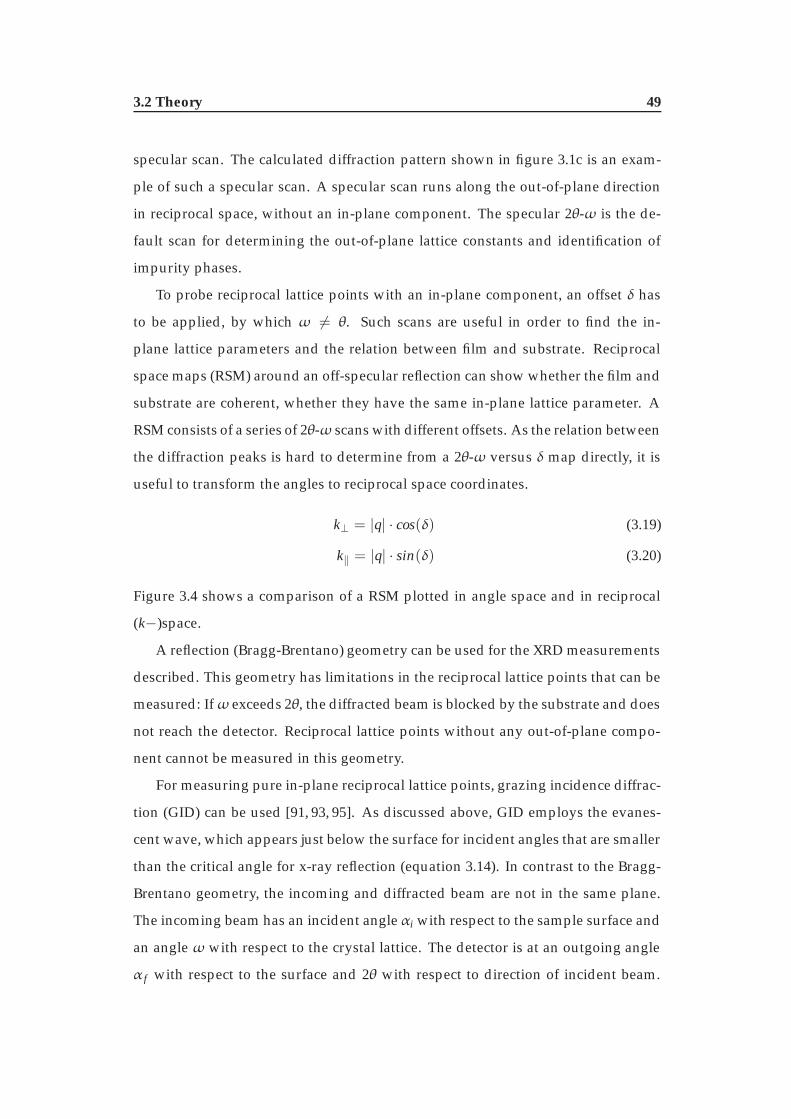
Figure 3.4 shows a comparison of a RSM plotted in angle space and in reciprocal
(k−)space.
A reflection (Bragg-Brentano) geometry can be used for the XRD measurements
described. This geometry has limitations in the reciprocal lattice points that can be
measured: Ifω exceeds 2θ, the diffracted beam is blocked by the substrate and does
not reach the detector. Reciprocal lattice points without any out-of-plane compo-
nent cannot be measured in this geometry.
For measuring pure in-plane reciprocal lattice points, grazing incidence diffrac-
tion (GID) can be used [91, 93, 95]. As discussed above, GID employs the evanes-
cent wave, which appears just below the surface for incident angles that are smaller
than the critical angle for x-ray reflection (equation 3.14). In contrast to the Bragg-
Brentano geometry, the incoming and diffracted beam are not in the same plane.
The incoming beam has an incident angleαi with respect to the sample surface and
an angleω with respect to the crystal lattice. The detector is at an outgoing angle
α f with respect to the surface and 2θ with respect to direction of incident beam.
50 X-Ray diffraction as a tool for characterization of ferroelectrics
� (o)
2�
(o)
14 16 18 20 22
71
72
73
74
75
76
77
78
79
k||/2k
0
K�/2
k0
0.14 0.16 0.18 0.2 0.22 0.24
0.53
0.54
0.55
0.56
0.57
0.58
0.59
0.6
0.61
0.62a) b)
Figure 3.4: A (1 0 3) RSM of a 7nm thick PbTiO3 film on SrTiO3. a) Plotted in angle space (δvs. 2θ). b) Plotted in reciprocal (k-) space. In k-space it is easily seen that both the film andsubstrate share the same k‖ and thus have the same in-plane lattice parameter
αi
αf
ω
2θ
a) b)
side view top view
x
z
x
y
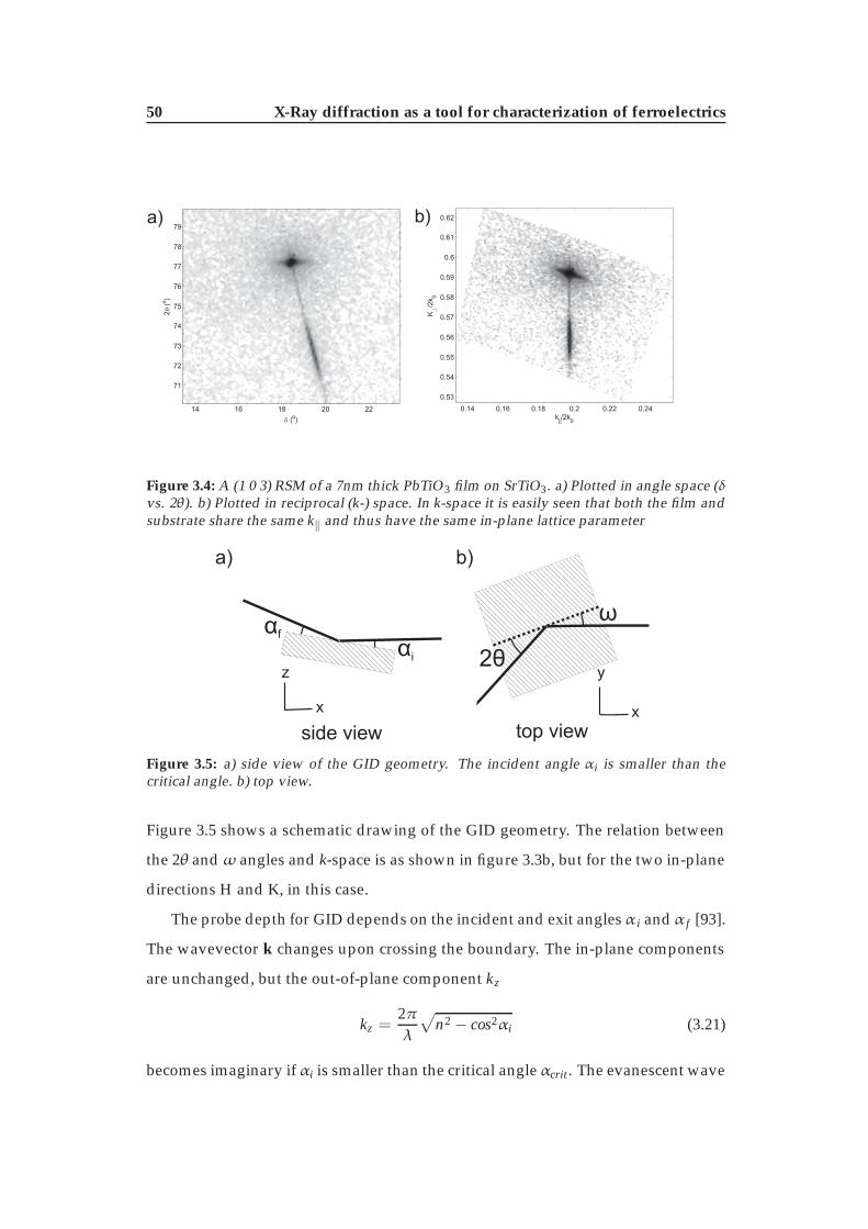
Figure 3.5: a) side view of the GID geometry. The incident angle αi is smaller than thecritical angle. b) top view.
Figure 3.5 shows a schematic drawing of the GID geometry. The relation between
the 2θ andω angles and k-space is as shown in figure 3.3b, but for the two in-plane
directions H and K, in this case.
The probe depth for GID depends on the incident and exit anglesα i andα f [93].
The wavevector k changes upon crossing the boundary. The in-plane components
are unchanged, but the out-of-plane component kz
kz =2πλ
√n2 − cos2αi (3.21)
becomes imaginary ifαi is smaller than the critical angleαcrit. The evanescent wave
3.3 Experimental setup 51
0 0.5 1 1.5 2100
101
102
αi / αcrit
Sca
tterin
g de
pth
(nm
)
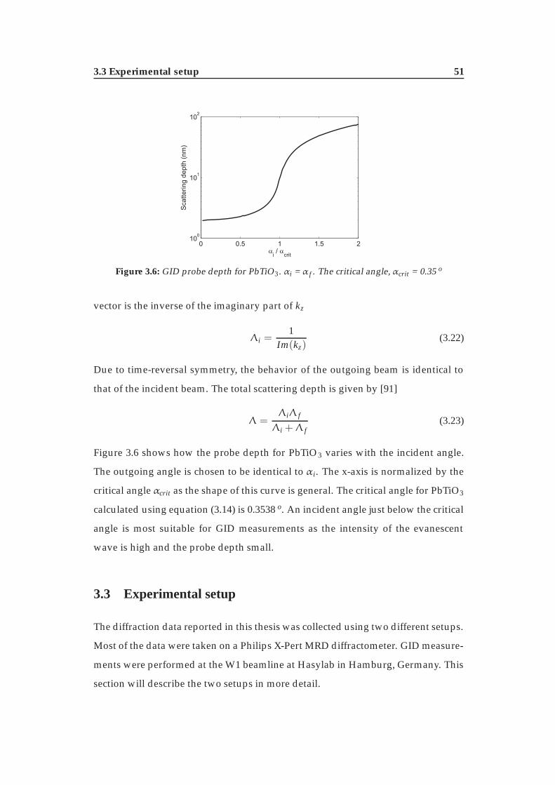
Figure 3.6: GID probe depth for PbTiO3. αi =α f . The critical angle,αcrit = 0.35 o
vector is the inverse of the imaginary part of kz
Λi =1
Im(kz)(3.22)
Due to time-reversal symmetry, the behavior of the outgoing beam is identical to
that of the incident beam. The total scattering depth is given by [91]
Λ =ΛiΛ f
Λi +Λ f(3.23)
Figure 3.6 shows how the probe depth for PbTiO3 varies with the incident angle.
The outgoing angle is chosen to be identical to α i. The x-axis is normalized by the
critical angleαcrit as the shape of this curve is general. The critical angle for PbTiO3
calculated using equation (3.14) is 0.3538 o. An incident angle just below the critical
angle is most suitable for GID measurements as the intensity of the evanescent
wave is high and the probe depth small.
3.3 Experimental setup
The diffraction data reported in this thesis was collected using two different setups.
Most of the data were taken on a Philips X-Pert MRD diffractometer. GID measure-
ments were performed at the W1 beamline at Hasylab in Hamburg, Germany. This
section will describe the two setups in more detail.
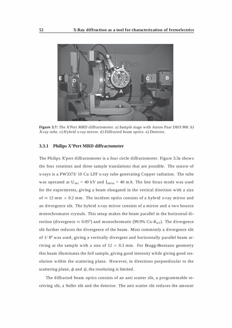
52 X-Ray diffraction as a tool for characterization of ferroelectrics
A
BCDE
Figure 3.7: The X’Pert MRD diffractometer. a) Sample stage with Anton Paar DHS 900. b)X-ray tube. c) Hybrid x-ray mirror. d) Diffracted beam optics. e) Detector.
3.3.1 Philips X’Pert MRD diffractometer
The Philips X’pert diffractometer is a four circle diffractometer. Figure 3.3a shows
the four rotations and three sample translations that are possible. The source of
x-rays is a PW3373/10 Cu LFF x-ray tube generating Copper radiation. The tube
was operated at Uacc = 40 kV and Iemiss = 40 mA. The line focus mode was used
for the experiments, giving a beam elongated in the vertical direction with a size
of ≈ 12 mm × 0.2 mm. The incident optics consists of a hybrid x-ray mirror and
an divergence slit. The hybrid x-ray mirror consists of a mirror and a two bounce
monochromator crystals. This setup makes the beam parallel in the horizontal di-
rection (divergence ≈ 0.05o) and monochromatic (99.9% Cu-Kα1). The divergence
slit further reduces the divergence of the beam. Most commonly a divergence slit
of 1/8o was used, giving a vertically divergent and horizontally parallel beam ar-
riving at the sample with a size of 12 × 0.3 mm. For Bragg-Brentano geometry
this beam illuminates the full sample, giving good intensity while giving good res-
olution within the scattering plane. However, in directions perpendicular to the
scattering plane,φ and ψ, the resoluting is limited.
The diffracted beam optics consists of an anti scatter slit, a programmable re-
ceiving slit, a Soller slit and the detector. The anti scatter slit reduces the amount
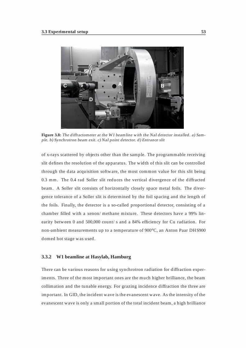
3.3 Experimental setup 53
A BC
D
Figure 3.8: The diffractometer at the W1 beamline with the NaI detector installed. a) Sam-ple. b) Synchrotron beam exit. c) NaI point detector. d) Entrance slit
of x-rays scattered by objects other than the sample. The programmable receiving
slit defines the resolution of the apparatus. The width of this slit can be controlled
through the data acquisition software, the most common value for this slit being
0.3 mm. The 0.4 rad Soller slit reduces the vertical divergence of the diffracted
beam. A Soller slit consists of horizontally closely space metal foils. The diver-
gence tolerance of a Soller slit is determined by the foil spacing and the length of
the foils. Finally, the detector is a so-called proportional detector, consisting of a
chamber filled with a xenon/methane mixture. These detectors have a 99% lin-
earity between 0 and 500,000 count/s and a 84% efficiency for Cu radiation. For
non-ambient measurements up to a temperature of 900oC, an Anton Paar DHS900
domed hot stage was used.
3.3.2 W1 beamline at Hasylab, Hamburg
There can be various reasons for using synchrotron radiation for diffraction exper-
iments. Three of the most important ones are the much higher brilliance, the beam
collimation and the tunable energy. For grazing incidence diffraction the three are
important. In GID, the incident wave is the evanescent wave. As the intensity of the
evanescent wave is only a small portion of the total incident beam, a high brilliance
54 X-Ray diffraction as a tool for characterization of ferroelectrics
is required.
At the Doris III storage ring at Hasylab in DESY, Hamburg, the energy of the
positrons is 4.45 GeV. The synchrotron radiation at the W1 beamline is created us-
ing a wiggler insertion device. The typical flux at the sample at an energy of 9
keV is 2×10¹¹ photons/sec [96]. The source to sample distance is 46m. A Si (111)
monochromator is used, giving an energy resolution of 2eV. The beam shape is de-
termined by a horizontal and vertical double slit system. An automatic attenuator
is used to maximize the dynamic range. A range up to 10 orders of magnitude can
be attained. In our case, the energy used for the diffraction experiments was either
9.8 keV or 8.048 keV, equivalent wavelengths of 1.2651 A and 1.540 (Cu kα1 radia-
tion) respectively. The diffractometer at W1 is a six-circle diffractometer. The two
extra circles when compared to the X’Pert lab diffractometer are required for GID
as the GID geometry is not coplanar. For the diffracted beam, two different detec-
tors have been used: A NaI(T1) point detector with crossed slits and an option for
an Germanium analyzer crystal and a linear detector. The linear ”Mythen” detector
has 1280 channels spanning a range of 4 o in 2θ [97]. The linear detector is highly
suitable for collecting reciprocal space maps in both the in-plane and out-of-plane
direction.
3.4 Tetragonality and Polarization
X-ray diffraction and reflectivity are routinely performed in thin film analysis for
determination of lattice parameters, thickness and roughness. The specific proper-
ties of (perovskite) ferroelectrics also allow the extraction of information about the
functional properties through XRD.
Early work on PbTiO3 showed a relation between lattice parameters and the
ferroelectric polarization [98, 99]. This relation was used by Haun et. al. for deter-
mining the Landau coefficients in the Gibbs free energy of PbTiO3 [34]. The tetrag-
onal, polar, phase of PbTiO3 can be considered as a distortion of the paraelectric
cubic phase. The tetragonality (c/a) is a measure for the size of this distortion. The
3.4 Tetragonality and Polarization 55
relation between the tetragonality and the polarization was shown to be: [100–102]
ca
=( c
a
)0+ constant · P2 (3.24)
Where( c
a
)0 is the tetragonality in the paraelectric phase. Equation (3.29) can be de-
rived in the framework of the Landau-Ginzburg expansion of the Helmholtz (con-
stant strain) free energy. 1 The definition of the out-of-plane strain is:
e33 =c f ilm − a f ilm
a f ilm(3.25)
combining the out-of-plane strain and the misfit strain, um, with the coherency con-
dition (a f ilm = asubstrate), the expression for the tetragonality becomes
c f ilm
asubstrate= (1 + e33)(1 + um) (3.26)
The out-of-plane strain is found from the Helmholtz free energy (U) through the
condition of zero out-of-plane stress ∂U∂e33
= 0.
∂U∂e33
= c11e33 + c122um − g11P2 = 0 (3.27)
e33 =g11P2 − 2c12um
c11(3.28)
combining equation (3.28) and equation (3.26) the relation between the polarization
and the tetragonality is found to be [102]
c f ilm
asubstrate=(
1 − 2c12um
c11
)(1 − um) +
(g11
c11
)(1 − um)P2 (3.29)
This expression only depends on the misfit strain (um) and the polarization (P). The
average magnitude of the polarization can now be determined from measurements
of the tetragonality.
Although equation 3.29 is correct, it breaks down at large compressive strains
for materials with a large shift of the A-ion, such as PbTiO3. [103] At very high com-
pressive strains the unit cell may still deform, giving rise to a large tetragonality,
but the Pb displacement is insensitive to the added strain. Therefore, care has to be
taken when using equation (3.29).1In contrast to the Gibbs energy, which is defined at constant stress (See section 1.4, the Helmholtz
free energy is defined at constant strain. The general form of the free energy expansion is similar, butthe coefficients coupling to the stress and strain respectively are different. The compliance, si j, andpolarization stress coupling, Qi j for the Gibbs free energy and the elastic constant, ci j and polarizationstrain coupling gi j for the Helmholtz free energy.
56 X-Ray diffraction as a tool for characterization of ferroelectrics
400 500 600 700 800
1.02
1.025
1.03
1.035
1.04
T (°C)
tetra
gona
lity
(c/a
)
21 nm PbTiO3 on SrTiO3
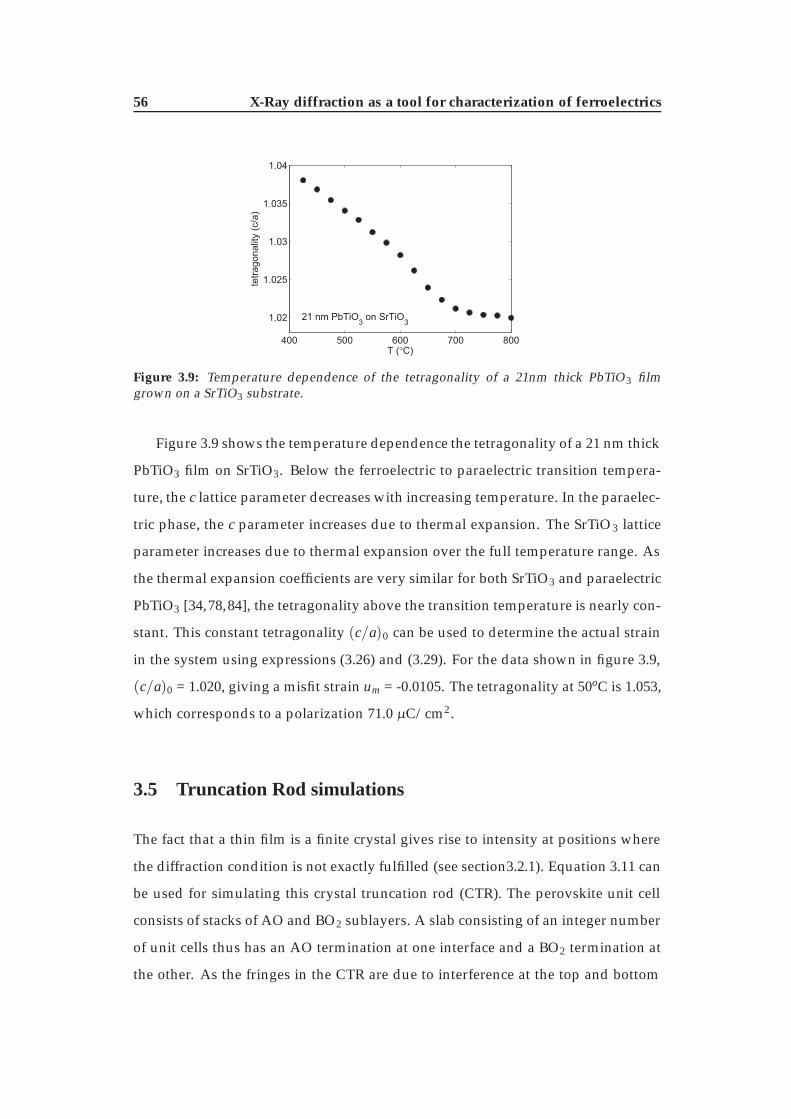
Figure 3.9: Temperature dependence of the tetragonality of a 21nm thick PbTiO3 filmgrown on a SrTiO3 substrate.
Figure 3.9 shows the temperature dependence the tetragonality of a 21 nm thick
PbTiO3 film on SrTiO3. Below the ferroelectric to paraelectric transition tempera-
ture, the c lattice parameter decreases with increasing temperature. In the paraelec-
tric phase, the c parameter increases due to thermal expansion. The SrTiO3 lattice
parameter increases due to thermal expansion over the full temperature range. As
the thermal expansion coefficients are very similar for both SrTiO3 and paraelectric
PbTiO3 [34,78,84], the tetragonality above the transition temperature is nearly con-
stant. This constant tetragonality (c/a)0 can be used to determine the actual strain
in the system using expressions (3.26) and (3.29). For the data shown in figure 3.9,
(c/a)0 = 1.020, giving a misfit strain um = -0.0105. The tetragonality at 50oC is 1.053,
which corresponds to a polarization 71.0 μC/cm2.
3.5 Truncation Rod simulations
The fact that a thin film is a finite crystal gives rise to intensity at positions where
the diffraction condition is not exactly fulfilled (see section3.2.1). Equation 3.11 can
be used for simulating this crystal truncation rod (CTR). The perovskite unit cell
consists of stacks of AO and BO2 sublayers. A slab consisting of an integer number
of unit cells thus has an AO termination at one interface and a BO2 termination at
the other. As the fringes in the CTR are due to interference at the top and bottom
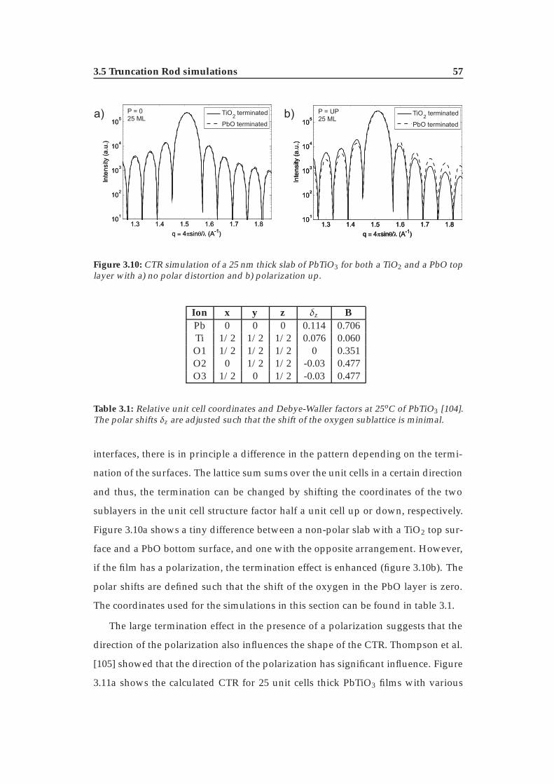
3.5 Truncation Rod simulations 57
1.3 1.4 1.5 1.6 1.7 1.810
1
102
103
104
105
q � 4�sin�/� (A-1
)
Inte
nsity
(a.u
.)
TiO2
terminated
PbO terminated
1.3 1.4 1.5 1.6 1.7 1.810
1
102
103
104
105
P = 025 ML
q � 4�sin�/� (A-1
)
Inte
nsity
(a.u
.)
TiO2
terminated
PbO terminated
1.3 1.4 1.5 1.6 1.7 1.810
1
102
103
104
105
q � 4�sin�/� (A-1
)
Inte
nsity
(a.u
.)
TiO2
terminated
PbO terminated
1.3 1.4 1.5 1.6 1.7 1.810
1
102
103
104
105
P = 025 ML
q � 4�sin�/� (A-1
)
Inte
nsity
(a.u
.)
TiO2
terminated
PbO terminated
1.3 1.4 1.5 1.6 1.7 1.810
1
102
103
104
105
P = UP25 ML
q � 4�sin�/� (A-1
)
Inte
nsity
(a.u
.)
TiO2
terminated
PbO terminated
a) b)
Figure 3.10: CTR simulation of a 25 nm thick slab of PbTiO3 for both a TiO2 and a PbO toplayer with a) no polar distortion and b) polarization up.
Ion x y z δz BPb 0 0 0 0.114 0.706Ti 1/2 1/2 1/2 0.076 0.060O1 1/2 1/2 1/2 0 0.351O2 0 1/2 1/2 -0.03 0.477O3 1/2 0 1/2 -0.03 0.477
Table 3.1: Relative unit cell coordinates and Debye-Waller factors at 25oC of PbTiO3 [104].The polar shifts δz are adjusted such that the shift of the oxygen sublattice is minimal.
interfaces, there is in principle a difference in the pattern depending on the termi-
nation of the surfaces. The lattice sum sums over the unit cells in a certain direction
and thus, the termination can be changed by shifting the coordinates of the two
sublayers in the unit cell structure factor half a unit cell up or down, respectively.
Figure 3.10a shows a tiny difference between a non-polar slab with a TiO2 top sur-
face and a PbO bottom surface, and one with the opposite arrangement. However,
if the film has a polarization, the termination effect is enhanced (figure 3.10b). The
polar shifts are defined such that the shift of the oxygen in the PbO layer is zero.
The coordinates used for the simulations in this section can be found in table 3.1.
The large termination effect in the presence of a polarization suggests that the
direction of the polarization also influences the shape of the CTR. Thompson et al.
[105] showed that the direction of the polarization has significant influence. Figure
3.11a shows the calculated CTR for 25 unit cells thick PbTiO3 films with various

58 X-Ray diffraction as a tool for characterization of ferroelectrics
polarities. These profiles are calculated using equation 3.11 and the intensity is
given by
I =∣∣xupAup + (1 − xup)Adown
∣∣2 (3.30)
where xup is the fraction of unit cells with up polarization and Aup and Adown are
the scattering amplitudes for an up and down polarized film, respectively. These
theoretical results show that it should be possible to obtain information about the
polarization direction and domain fractions from fitting measured CTR profiles.
The tetragonality can be obtained from the same CTR profile provided the film is
coherently strained to a cubic substrate. Thus, if the polarization is along c, the
magnitude and direction of the polarization, as well as the distribution of domains
can be obtained from a single XRD measurement.
The polarization effect on the CTR profiles is caused by interference at the inter-
faces. For perovskite thin films in general, and ferroelectric perovskites specifically,
there are various interface properties that may have similar influence on the CTR
profile. The calculated CTR profiles around the (001) and (002) peaks are shown for
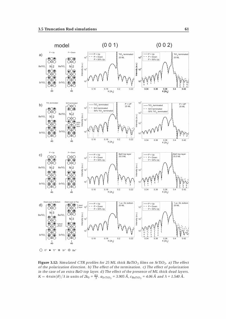
PbTiO3 (fig. 3.11) and tetragonal BaTiO3 (fig. 3.12) on SrTiO3 with various surfaces
and interfaces. PbTiO3 is an A-site ferroelectric, meaning that the polar shift is car-
ried mainly by the central Pb ion, whereas BaTiO3 is a B-site ferroelectric, where
the distortion of the TiO6 octahedra gives rise to the polarization. As the number
of electrons in Pb is much higher than that of Ti, it is expected that the polarization
effect on the truncation rods is much larger for PbTiO3. Moreover, the magnitude
of the ion shifts is also much larger for PbTiO3.
Figures 3.11a and 3.12a show the effect of polarization for a TiO2 terminated
substrate and a 25 ML TiO2 terminated layer, as shown in the schematic diagram.
For PbTiO3 there is a clear difference between up and down polarization, most
clearly visible at the high q side of the Bragg peak. Mixed polarization leads to
an overall decrease of the intensity coming from the film, showing that there is
a large phase difference between the scattering amplitudes of the up and down
polarization. These observations are in agreement with what Thompson et al. re-
ported based on similar simulations [105]. In BaTiO3 the polarization effect is much

3.5 Truncation Rod simulations 59
smaller. However it is still present, especially at higher q values. The large de-
crease in overall film intensity for mixed polarization as observed in PbTiO3, is not
present.
Although SrTiO3 can be treated to obtain a single TiO2 termination (see section
2.4.1), it is very interesting to see the effect of substrate termination on the CTR
profile. For many perovskite substrates, no treatment able to provide a single ter-
mination is available. Even if a treatment is available, a 100% single termination
is very hard to obtain. Figures 3.11b and 3.12b show how substrate termination
influcences the CTR profiles for PbTiO3 and BaTiO3, respectively. SrO termination
is modelled by adding a SrO monolayer at the substrate film interface. A SrO ter-
minated SrTiO3 substrate also implies an inversion of the film stacking, giving rise
to an AO terminated film surface. For PbTiO3 (fig. 3.11b), the effect of substrate ter-
mination is small compared to the polarization effect. BaTiO3 (fig. 3.12b) shows a
relatively large substrate termination effect around the (001) peak, around the (002)
peak, however the effect is much smaller.
In the MBE growth of PbTiO3 a continuous flux of PbO is used because the
growth is adsorption controlled (see chapter 2.5). This typically leads to a PbO
terminated layer with a thickness of N+ 12 monolayers. The CTR profiles for such
films are shown in figure 3.11c, in order to see if this influences the polarization
effect. From the comparison of figures 3.11c and 3.12c with figures 3.11a and 3.12a,
it is clear that the extra PbO or BaO layer has no qualitative influence on the po-
larization effect on either PbTiO3 or BaTiO3. However, the extra half unit cell does
increase the thickness and for simulation of real experimental data, it has to be
taken into account.
A dead layer is a sublayer with no polarization and can occur in ferroelectric
thin films at the electrode interface. [106] The influence of a very thin dead layer of
only one unit cell at either the top or bottom interface has been modeled. Although
the dead layer in a real sample can be much thicker, figures 3.11d and 3.12d show
that for both PbTiO3 and BaTiO3 the presence of a one unit cell dead layer has
a considerable impact on the CTR profile. The much smaller effect on BaTiO3 is
consistent with the much smaller polar shift and thus, a smaller difference between
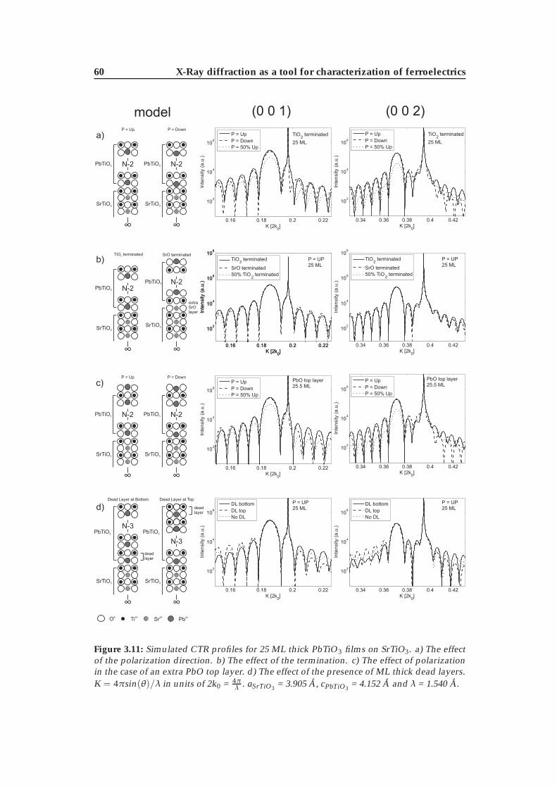
60 X-Ray diffraction as a tool for characterization of ferroelectrics
0.16 0.18 0.2 0.22
102
104
106
108
P = UP25 ML
K [2k0]
Inte
nsity
(a.u
.)
TiO2
terminated
SrO terminated
50% TiO2
terminated
0.16 0.18 0.2 0.22
102
104
106
108
P = UP25 ML
K [2k0]
Inte
nsity
(a.u
.)
TiO2
terminated
SrO terminated
50% TiO2
terminated
b)
N-2
∞ ∞
N-2PbTiO3
SrTiO3
PbTiO3
SrTiO3
extraSrOlayer
SrO terminatedTiO terminated2
a)
N-2
∞
PbTiO3
SrTiO3
P = Up
N-2
∞
PbTiO3
SrTiO3
P = Down
d)
O2-
Ti4+
Sr2+
Pb4+
∞
PbTiO3
SrTiO3
N-3
∞
PbTiO3
SrTiO3
N-3
deadlayer
deadlayer
Dead Layer at Bottom Dead Layer at Top
0.34 0.36 0.38 0.4 0.42
102
104
106
TiO2
terminated
25 ML
K [2k0]
Inte
nsity
(a.u
.)
P = Up
P = Down
P = 50% Up
0.34 0.36 0.38 0.4 0.42
102
104
106
108
P = UP25 ML
K [2k0]
Inte
nsity
(a.u
.)
TiO2
terminated
SrO terminated
50% TiO2
terminated
0.16 0.18 0.2 0.22
102
104
106
TiO2
terminated
25 ML
K [2k0]
Inte
nsity
(a.u
.)
P = Up
P = Down
P = 50% Up
c)
N-2
∞
PbTiO3
SrTiO3
P = Up
N-2
∞
PbTiO3
SrTiO3
P = Down
0.16 0.18 0.2 0.22
102
104
106
PbO top layer25.5 ML
K [2k0]
Inte
nsity
(a.u
.)
P = Up
P = Down
P = 50% Up
0.34 0.36 0.38 0.4 0.42
102
104
106
PbO top layer25.5 ML
K [2k0]
Inte
nsity
(a.u
.)
P = Up
P = Down
P = 50% Up
(0 0 1) (0 0 2)model
0.34 0.36 0.38 0.4 0.42
102
104
106
P = UP25 ML
K [2k0]
Inte
nsity
(a.u
.)
DL bottom
DL top
No DL
0.16 0.18 0.2 0.22
102
104
106
P = UP25 ML
K [2k0]
Inte
nsity
(a.u
.)
DL bottom
DL top
No DL
Figure 3.11: Simulated CTR profiles for 25 ML thick PbTiO3 films on SrTiO3. a) The effectof the polarization direction. b) The effect of the termination. c) The effect of polarizationin the case of an extra PbO top layer. d) The effect of the presence of ML thick dead layers.K = 4πsin(θ)/λ in units of 2k0 = 4π
λ . aSrTiO3 = 3.905 A, cPbTiO3= 4.152 A and λ = 1.540 A.
3.5 Truncation Rod simulations 61
0.34 0.36 0.38 0.4 0.42
102
104
106
108
P = UP25 ML
K [2k0]
Inte
nsity
(a.u
.)
TiO2
terminated
SrO terminated
50% TiO2
terminated
0.16 0.18 0.2 0.22
102
104
106
P = UP25 ML
K [2k0]
Inte
nsity
(a.u
.)
TiO2
terminated
SrO terminated
50% TiO2
terminated
0.16 0.18 0.2 0.22
102
104
106
BaO top layer25.5 ML
K [2k0]
Inte
nsity
(a.u
.)
P = Up
P = Down
P = 50% Up
0.34 0.36 0.38 0.4 0.42
102
104
106
BaO top layer25.5 ML
K [2k0]
Inte
nsity
(a.u
.)
P = Up
P = Down
P = 50% Up
0.34 0.36 0.38 0.4 0.42
102
104
106
1 uc. DL bottom25 ML
K [2k0]
Inte
nsity
(a.u
.)
P = Up
P = Down
P = 50% Up
0.16 0.18 0.2 0.22
102
104
106
1 uc. DL bottom25 ML
K [2k0]
Inte
nsity
(a.u
.)
P = Up
P = Down
P = 50% Up
0.34 0.36 0.38 0.4 0.42
102
104
106
TiO2
terminated
25 ML
K [2k0]
Inte
nsity
(a.u
.)
P = Up
P = Down
P = 50% Up
0.34 0.36 0.38 0.4 0.42
102
104
106
TiO2
terminated
25 ML
K [2k0]
Inte
nsity
(a.u
.)
P = Up
P = Down
P = 50% Up
0.16 0.18 0.2 0.22
102
104
106
TiO2
terminated
25 ML
K [2k0]
Inte
nsity
(a.u
.)
P = Up
P = Down
P = 50% Up
b)
N-2
∞ ∞
N-2BaTiO3
SrTiO3
BaTiO3
SrTiO3
extraSrOlayer
SrO terminatedTiO terminated2
a)
N-2
∞
BaTiO3
SrTiO3
P = Up
N-2
∞
BaTiO3
SrTiO3
P = Down
d)
∞
BaTiO3
SrTiO3
N-3
∞
BaTiO3
SrTiO3
N-3
deadlayer
deadlayer
Dead Layer at Bottom Dead Layer at Top
c)
N-2
∞
BaTiO3
SrTiO3
P = Up
N-2
∞
BaTiO3
SrTiO3
P = Down
(0 0 1) (0 0 2)model
O2-
Ti4+
Sr2+
Ba4+
Figure 3.12: Simulated CTR profiles for 25 ML thick BaTiO3 films on SrTiO3. a) The effectof the polarization direction. b) The effect of the termination. c) The effect of polarizationin the case of an extra BaO top layer. d) The effect of the presence of ML thick dead layers.K = 4πsin(θ)/λ in units of 2k0 = 4π
λ . aSrTiO3 = 3.905 A, cBaTiO3 = 4.06 A and λ = 1.540 A.

62 X-Ray diffraction as a tool for characterization of ferroelectrics
a polar and a non polar ”dead” unit cell. An important difference between the
effect of dead layers when compared to the polarization effect is that the dead layer
effect is as clearly present on both the high q and low q sides of the Bragg peaks,
whereas the polarization effect is most clear on the high q side.
Closure domains in 180o domain structures, in which the polarization is parallel
to the surface at the top and bottom interfaces [107], are expected to have similar
effect as dead layers on the simulations because they lead to a few unit cells without
out-of-plane polarization. Effects opposite to dead layers have also been proposed,
such as a polar shift occurring in a few unit cells of the the substrate close to the
interface [108] or enhanced polarization at the interfaces [27]. All these effects are
expected to have a similar large influence on the CTR profile.
The large number of interface properties all having an influence on the CTR
profile complicates the application of the model to experimental data. To reduce
the number of parameters, some assumptions have to be made. Moreover, rough-
ness and thickness variations, typical for real samples, have to be included in the
model. The assumptions used for modeling MBE grown PbTiO3 thin films on
SrTiO3 are a perfect TiO2 termination for the SrTiO3 substrate, a complete PbO
termination on the top surface and no dead layers. The roughness is included by
using a Gaussian roughness factor, exp[−0.5σ2(q − q00L)2], that was applied to the
substrate and film scattering amplitudes. Here, q00L = 2πLc , where c is replaced
by a in the case of the substrate. Thickness variations are included by calculating
the total scattering amplitude for a range of thicknesses and adding these using
〈Atotal〉 = ∑i p(Ni)Ftotal(Ni), where p(Ni) is the probability, based on a normal dis-
tribution with a standard deviation σN , for the film to have a thickness Ni. The
MATLAB code used for the simulation of the experimental data can be found in
Appendix A.
An example of these simulations is found in figure 3.13. Simulations of the
same data are shown, using identical parameters except for the fraction of unit
cells with polarization up. The best fit is shown in figure 3.13a and has a 80% of the
polarization pointing up. The first fringe on the right side of the substrate peak is
the feature most sensitive to the polarization direction.

3.6 Periodic domains in XRD 63
18 19 20 21 22 23 24 25
100
102
104
106
Inte
nsity
(a.u
.)
2�(�)
18 19 20 21 22 23 24 25
100
102
104
106
Inte
nsity
(a.u
.)
2�(�)
18 19 20 21 22 23 24 25
100
102
104
106
Inte
nsity
(a.u
.)
2�(�)
b)a)
c)
P = 80% Up
P = Up
P = Down
Figure 3.13: Simulations of experimental data of a 22nm thick PbTiO3 film on SrTiO3. a)80% of the domains pointing up. b) 100% up polarized. c) 100% down polarized.
3.6 Periodic domains in XRD
Ferroelectric domains can order periodically due to the competition between depo-
larization field and domain wall energy, similar to ferromagnetic materials. [14,22]
This periodicity can be observed using x-ray diffraction techniques. Streiffer et al.
used in-situ synchrotron radiation to observe 180o domains oriented along the c
direction, upon cooling down from the growth temperature [15] The presence of
periodic domain structures was used as evidence that the ferroelectric distortion in
PbTiO3 is stable down to 3 unit cells in polydomain films. [31]
There is a difference in unit cell structure factor between unit cells with different
polarization directions. If there is no difference in lattice parameters, which is the
case with 180o domains, this is not easily observed. However, if the 180o domains
order periodically, the resulting periodic difference in structure factor between both
domains leads to extra diffraction peaks. In the direction perpendicular to the 180o
domain walls, a pair of up and down domains can be considered as a unit cell of
the superstructure. Whether the superstructure peaks can be observed depends on
the direction of the polarization. The structure factor (section 3.2.1) of a unit cell is
64 X-Ray diffraction as a tool for characterization of ferroelectrics
given by
FUC(q) = ∑ f j(q)ei(qx·xj+qy·yj+qz·z j) (3.31)
where f j(q) are the atomic form factors and the sum is over the atoms of one unit
cell. From equation (3.31) it can be seen that, for a polarization that is along z, qz
must be non-zero for the superstructure to be visible. Thus periodic 180o domains
can be observed along the reciprocal lattice vector of the domain structure, only
around a film peak with an out-of-plane component of the scattering vector.
The approach for calculating truncation rods as described in section 3.2.1 was
extended to two dimensions. The scattering amplitude of a film plus substrate
CTR was taken as the new unit for a lattice sum which runs over the width of
a single domain. When this single domain is added to the oppositely polarized
domain using the correct phase shift, the scattering amplitude of a single domain
period is obtained. This domain period scattering amplitude is then summed from
0 to infinity. To maintain the symmetry of the substrate, the intensities of domain
periodicities along one in-plane direction as well as the perpendicular direction are
added. This gives rise to the fourfold symmetry observed in the simulations in
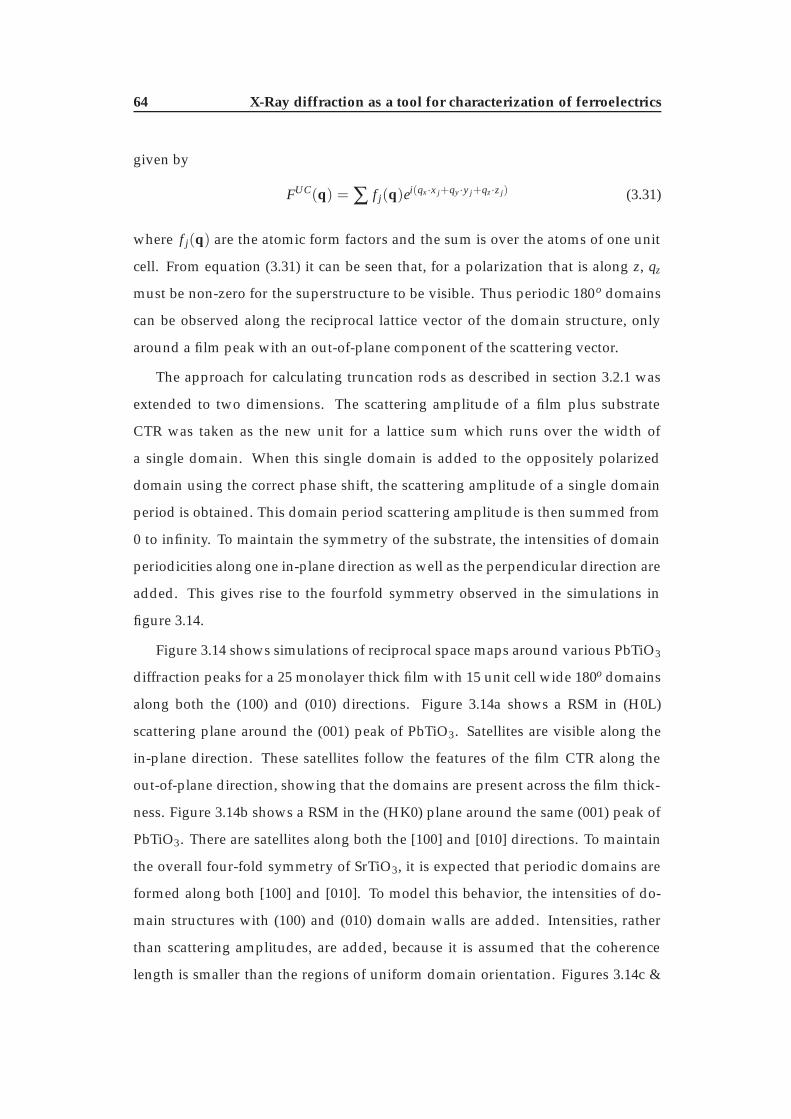
figure 3.14.
Figure 3.14 shows simulations of reciprocal space maps around various PbTiO3
diffraction peaks for a 25 monolayer thick film with 15 unit cell wide 180o domains
along both the (100) and (010) directions. Figure 3.14a shows a RSM in (H0L)
scattering plane around the (001) peak of PbTiO3. Satellites are visible along the
in-plane direction. These satellites follow the features of the film CTR along the
out-of-plane direction, showing that the domains are present across the film thick-
ness. Figure 3.14b shows a RSM in the (HK0) plane around the same (001) peak of
PbTiO3. There are satellites along both the [100] and [010] directions. To maintain
the overall four-fold symmetry of SrTiO3, it is expected that periodic domains are
formed along both [100] and [010]. To model this behavior, the intensities of do-
main structures with (100) and (010) domain walls are added. Intensities, rather
than scattering amplitudes, are added, because it is assumed that the coherence
length is smaller than the regions of uniform domain orientation. Figures 3.14c &
3.6 Periodic domains in XRD 65
kx/2k
0
k y/2k 0
0.19 0.195 0.2 0.205
0.19
0.195
0.2
0.205
kx/2k
0
k y/2k 0
0.19 0.195 0.2 0.205
0.19
0.195
0.2
0.205
kx/2k
0
k z/2k 0
-5 0 5
x 10-3
0.32
0.34
0.36
0.38
0.4
0.42b)a)
c) d)
(H0L) plane around (001) (HK0) plane around (001)
(HK0) plane around (111) (HK0) plane around (110)
kx/2k
0
k y/2k 0
-5 0 5
x 10-3
-8
-6
-4
-2
0
2
4
6
8
x 10-3
Figure 3.14: RSM simulations of periodic 180o domain structures. a) Around the (001)reflection in the out of plane direction. b) In-plane RSM around the (001) c) In-plane RSMaround (111) d) In-plane RSM around (110), showing no satellites as there is no out-of-planecomponent to the scattering vector.
d illustrate the difference between scattering vectors with and without an out-of-
plane component. While figure 3.14c shows satellites, similar to figure 3.14b, figure
3.14d shows no superstructure.
The spacing between the satellites and the Bragg peak gives the domain peri-
odicity [109]
Λ =λ
2Δk(3.32)
where Δk is expressed in terms of 2k0(=4π/λ) and λ is the x-ray wavelength. In
the case of perfect 180o domains, where the fractions of up and down domains
are exactly equal, only the odd orders of the satellites are observed. If there is a
majority polarization, the even orders should be visible as well [15].
66 X-Ray diffraction as a tool for characterization of ferroelectrics
-0.02 -0.01 0 0.01
100
101
102
103
104
105
106
107
108
KParallel [2k0]
Inte
nsity
(a.u
)
700oC
625oC
550oC
350oC
50oC
-0.015 -0.01 -0.005 0 0.005 0.01 0.015
100
101
102
103
K [2k ]
Inte
nsity
(a.u
)
50o C, before heating50o C, after heating
b)a)
Figure 3.15: a) Temperature evolution of the satellite peaks. The satellites disappear aboveTC, but reappear upon cooling (b).
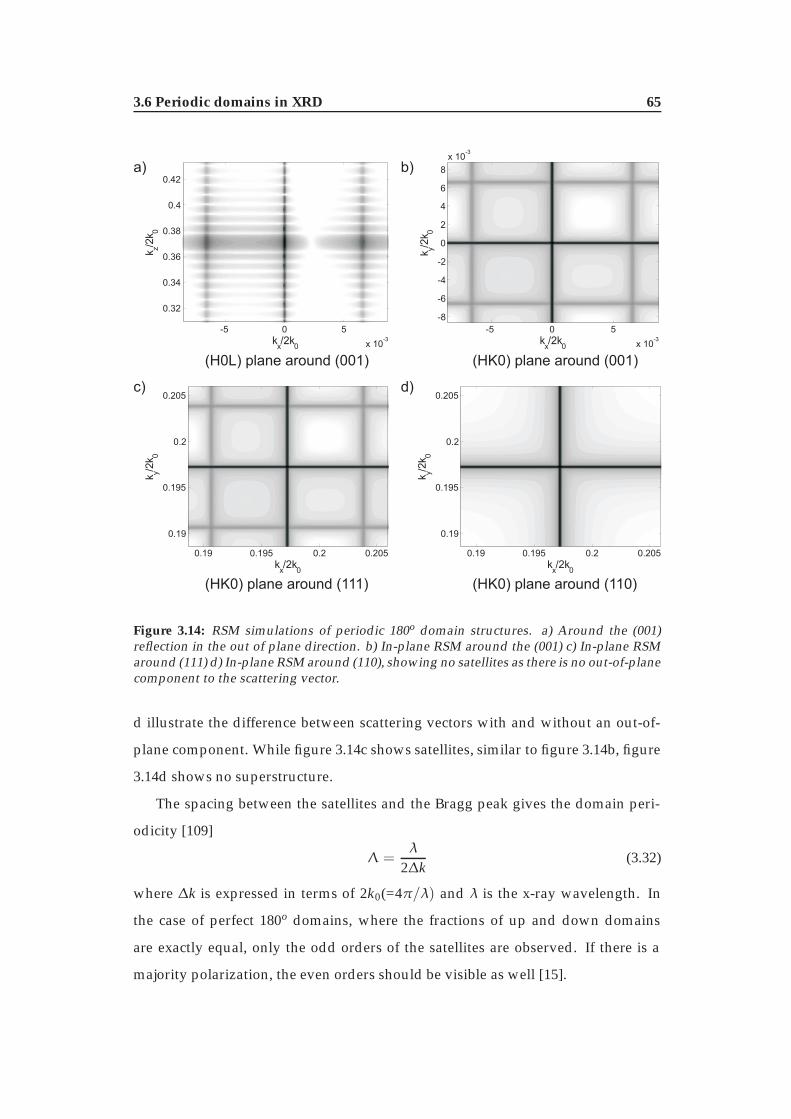
Figure 3.15 shows the temperature evolution of the satellite peaks observed dur-
ing this thesis work in a 18 nm thick Pb0.97Sr0.03Ti3 thin film grown on SrTiO3. At
50oC the satellite spacing is Δk ≈ 0.044, which corresponds to a domain periodicity
Λ = 17.5 nm. With increasing temperature there is little change in satellite spacing,
but a decrease in intensity is observed. Above TC ≈ 625oC, the satellites have com-
pletely disappeared. Upon cooling the film, the satellites reappear at exactly the
same spacing (figure 3.15b).
The small extent of change in domain periodicity with increasing temperature
seems remarkable in the light of theories on equilibrium domain structures [14,
15, 22]. Based on these theories, one would expect the domain periodicity to scale
with the polarization and thus with temperature. However, no clear shift of the
satellites is observed. A possible explanation for this is that a change in the overall
periodicity would imply quite large domain wall shifts. A 1 nm increase in one
period seems small, but it implies a shift of 100 nm for the domain wall which
is 100 periods away. Such big shifts can be kinetically unfavorable. The fact that
exactly the same domain periodicity is recovered after cooling may have the same
origin: The domain structure forms below TC and its periodicity does not change
anymore upon cooling further.
Simulations of the reciprocal space maps of periodic domain structures, such
as shown in figure 3.14, are very useful for determining the domain structure and
polarization direction. The presence or absence of satellites in certain directions

3.7 Conclusion 67
and positions in q-space depends on both the domain structure and direction of
the polarization in the domains. The absence of satellites at peaks without an out-
of-plane component (see figure 3.14d), in case of c-oriented 180o domains, is an
example of this.
Simulations of periodic domain structures in ferroelectrics were also reported
by Takahashi et al. [110] The focus of their simulations was towards domain ran-
domness and domain compensation. The main result from their simulations is that
the width of the satellite peaks increases if there are random variation in the domain
width. Moreover, the apparent Δk (the peak maximum) shifts to smaller values.
This shift is important to bear in mind when interpreting experimental data.
3.7 Conclusion
X-ray diffraction can be used as a probe for ferroelectricity in various ways. The
tetragonality can give the magnitude of the polarization of the unit cell, and its
temperature dependence. In sufficiently smooth films analysis and simulation of
the specular scans can give information on the direction of the polarization and
fractions of domains. Additionally, if the domains are periodic, the presence of
satellites can give information about the domain periodicity as well as the direc-
tion of the polarization. However, as all described methods are indirect probes of
the polarization and modeling is required to analyze the data, care has to be taken
when interpreting the data. The ability to extract the polarization, the transition
temperature, the direction of the polarization and domain structure from measure-
ments not requiring electrodes is very convenient for studying effects of strain,
where the addition of an electrode layer adds to the complexity of the system, both
in growth and the analysis of the strain.