UNIVERSITY OF CALGARY Fault-tolerant Architectures for Nanowire and Quantum Array Devices
182
UNIVERSITY OF CALGARY Fault-tolerant Architectures for Nanowire and Quantum Array Devices by Tamer S. Mohamed A THESIS SUBMITTED TO THE FACULTY OF GRADUATE STUDIES IN PARTIAL FULFILLMENT OF THE REQUIREMENTS FOR THE DEGREE OF DOCTOR OF PHILOSOPHY DEPARTMENT OF ELECTRICAL AND COMPUTER ENGINEERING CALGARY, ALBERTA April, 2013 c Tamer S. Mohamed 2013
Transcript of UNIVERSITY OF CALGARY Fault-tolerant Architectures for Nanowire and Quantum Array Devices

UNIVERSITY OF CALGARY
Fault-tolerant Architectures for Nanowire and Quantum Array Devices
by
Tamer S. Mohamed
A THESIS
SUBMITTED TO THE FACULTY OF GRADUATE STUDIES
IN PARTIAL FULFILLMENT OF THE REQUIREMENTS FOR THE
DEGREE OF DOCTOR OF PHILOSOPHY
DEPARTMENT OF ELECTRICAL AND COMPUTER ENGINEERING
CALGARY, ALBERTA
April, 2013
c© Tamer S. Mohamed 2013

Abstract
This work investigates techniques for building fault-tolerant digital circuits at the nano-
scale. It provides an overview of some nano-scale technology candidates that can be used
in the next generation of digital circuit based on nanoelectronic logic fabrics. It focuses on
fault tolerance of such circuits at both the circuit and the architecture level. A case study
based on pass-transistor logic using wrap-gate nanowire devices is presented. Such circuits
implement logic computing in the form of binary decision diagrams (BDDs), however, they
are not fault-immune. In this thesis, the BDD based nanowire devices that incorporate er-
ror correction coding are proposed. In addition, a planarization algorithm is presented and
implemented in order to synthesize planar error correcting circuits using such devices. Al-
ternative architecture, such as the cross-bar nano-FPGA, is considered as another candidate
for fault-tolerance. Simulation and modeling of all the presented architectures are performed
using the developed software “BDD processing tool”, CUDD package and SPICE.
i

Acknowledgements
alh.mdo lillahi rbbi alalamyn
áÖÏ A ªË @ H. P é
<Ë
YÒmÌ'@
I would like to thank Dr. S Yanushkevich, my supervisor for her help, her great patience
and support in finishing this work. I would also like to thank Dr. Graham Jullien and Dr.
Vassil Dimitrov for their help, support and very enlightening discussions. My wife and my
parents provided me with love, encouragement and faith. I hope I will be able to fulfil my
promises to them. My friends were always by my side encouraging me and I am indebted
to them in many ways. My friend, Hazem Gomaa, gave me very helpful comments and
feedback about my presentation. I would also like to thank Dr. Anton Zeilinger who, during
his visit to Calgary, patiently answered my questions about Quantum entanglement. Dr.
D. Michael Miller, my external examiner, gave me encouraging remarks and inspiring ideas
about future research. I would also like to thank the University of Calgary, and the funding
agencies; NSERC, AIF and iCore for the financial support. Many thanks are also due to
the most helpful and cheerful staff working in the Electrical Engineering department at the
University. Thank you Lisa Bensmiller, Judy Trumble and Ella Lok.
ii
Table of Contents
Abstract i
Acknowledgements ii
Table of Contents iii
List of Tables vi
List of Figures and Illustrations vii
List of Symbols, Abbreviations and Nomenclature x
1 Introduction 11.1 Research Motivation . . . . . . . . . . . . . . . . . . . . . . . . . . . . . . . 11.2 Research Objectives . . . . . . . . . . . . . . . . . . . . . . . . . . . . . . . . 21.3 Research Outcomes . . . . . . . . . . . . . . . . . . . . . . . . . . . . . . . . 2
2 Nanoelectronic Logic Fabric 42.1 Introduction . . . . . . . . . . . . . . . . . . . . . . . . . . . . . . . . . . . . 42.2 Types of materials for nano electronics . . . . . . . . . . . . . . . . . . . . . 6
2.2.1 Carbon in nano electronics . . . . . . . . . . . . . . . . . . . . . . . . 62.2.2 Unimolecular compound materials . . . . . . . . . . . . . . . . . . . . 7
2.3 Devices not modeled by conventional charge transport . . . . . . . . . . . . . 92.3.1 III-IV Quantum devices . . . . . . . . . . . . . . . . . . . . . . . . . 102.3.2 Quantum cellular automata . . . . . . . . . . . . . . . . . . . . . . . 102.3.3 Quantum computation . . . . . . . . . . . . . . . . . . . . . . . . . . 11
2.4 Device assembly techniques . . . . . . . . . . . . . . . . . . . . . . . . . . . 122.5 Circuit architectures and defect tolerance . . . . . . . . . . . . . . . . . . . . 132.6 Conclusion . . . . . . . . . . . . . . . . . . . . . . . . . . . . . . . . . . . . . 14
3 Overview of Fault Tolerance 153.1 Introduction . . . . . . . . . . . . . . . . . . . . . . . . . . . . . . . . . . . . 153.2 Definitions . . . . . . . . . . . . . . . . . . . . . . . . . . . . . . . . . . . . . 163.3 Construction of fault tolerant systems . . . . . . . . . . . . . . . . . . . . . . 173.4 Fault tolerance via hardware redundancy . . . . . . . . . . . . . . . . . . . . 173.5 Fault tolerance via information redundancy . . . . . . . . . . . . . . . . . . . 203.6 Fault tolerance via probabilistic computing . . . . . . . . . . . . . . . . . . . 213.7 Fault tolerance via algorithmic/approximate computing . . . . . . . . . . . . 223.8 Fault tolerance via time redundancy . . . . . . . . . . . . . . . . . . . . . . . 223.9 Fault tolerance via energy minimization . . . . . . . . . . . . . . . . . . . . . 233.10 Fault Tolerance via reconfiguration . . . . . . . . . . . . . . . . . . . . . . . 233.11 Fault Tolerance via dynamic routing . . . . . . . . . . . . . . . . . . . . . . 243.12 Performance measures . . . . . . . . . . . . . . . . . . . . . . . . . . . . . . 25
iii

3.12.1 Kullback-Leibler divergence . . . . . . . . . . . . . . . . . . . . . . . 253.12.2 Signal-to-noise ratio (SNR) . . . . . . . . . . . . . . . . . . . . . . . 263.12.3 Bit error rate (BER) . . . . . . . . . . . . . . . . . . . . . . . . . . . 26
3.13 Performance analysis techniques . . . . . . . . . . . . . . . . . . . . . . . . . 263.14 Conclusion . . . . . . . . . . . . . . . . . . . . . . . . . . . . . . . . . . . . . 27
4 BDD-based Nanowire Error Correcting Circuits 284.1 Introduction . . . . . . . . . . . . . . . . . . . . . . . . . . . . . . . . . . . . 284.2 Background . . . . . . . . . . . . . . . . . . . . . . . . . . . . . . . . . . . . 294.3 Gate reliability without error correction . . . . . . . . . . . . . . . . . . . . . 314.4 Probabilistic error model in a binary decision diagram . . . . . . . . . . . . . 35
4.4.1 Input Error Probability and SNR . . . . . . . . . . . . . . . . . . . . 434.5 Error-correction coding . . . . . . . . . . . . . . . . . . . . . . . . . . . . . . 45
4.5.1 Shortened codes . . . . . . . . . . . . . . . . . . . . . . . . . . . . . . 474.6 BDD model with error correction . . . . . . . . . . . . . . . . . . . . . . . . 484.7 Reliability of the error-correcting BDD . . . . . . . . . . . . . . . . . . . . . 564.8 Experiments . . . . . . . . . . . . . . . . . . . . . . . . . . . . . . . . . . . . 604.9 Conclusion . . . . . . . . . . . . . . . . . . . . . . . . . . . . . . . . . . . . . 66
5 Synthesis of Planar Nano-Circuits 675.1 Introduction . . . . . . . . . . . . . . . . . . . . . . . . . . . . . . . . . . . . 675.2 Algorithm 1: Linear-time node processing . . . . . . . . . . . . . . . . . . . 715.3 Algorithm 2: Multi-pass diagram processing . . . . . . . . . . . . . . . . . . 735.4 Results . . . . . . . . . . . . . . . . . . . . . . . . . . . . . . . . . . . . . . . 755.5 Conclusions . . . . . . . . . . . . . . . . . . . . . . . . . . . . . . . . . . . . 76
6 Crossbar Latch-based Combinational and Sequential Logic for nano FPGA 786.1 Introduction . . . . . . . . . . . . . . . . . . . . . . . . . . . . . . . . . . . . 786.2 Device modeling . . . . . . . . . . . . . . . . . . . . . . . . . . . . . . . . . . 796.3 Operation model of the crossbar latch . . . . . . . . . . . . . . . . . . . . . . 816.4 Combinational circuit models . . . . . . . . . . . . . . . . . . . . . . . . . . 876.5 Sequential circuits . . . . . . . . . . . . . . . . . . . . . . . . . . . . . . . . . 896.6 Organization of a nano FPGA using crossbar arrays . . . . . . . . . . . . . . 916.7 Area and timing of the nano FPGA . . . . . . . . . . . . . . . . . . . . . . . 956.8 Fault and defect Tolerance in nano FPGA . . . . . . . . . . . . . . . . . . . 996.9 Conclusion . . . . . . . . . . . . . . . . . . . . . . . . . . . . . . . . . . . . . 101
7 Quantum Computing Alternative 1037.1 Introduction . . . . . . . . . . . . . . . . . . . . . . . . . . . . . . . . . . . . 103
7.1.1 The qubit . . . . . . . . . . . . . . . . . . . . . . . . . . . . . . . . . 1057.1.2 A system of more than one qubit . . . . . . . . . . . . . . . . . . . . 1097.1.3 Entanglement . . . . . . . . . . . . . . . . . . . . . . . . . . . . . . . 1107.1.4 Quantum gates . . . . . . . . . . . . . . . . . . . . . . . . . . . . . . 1127.1.5 Matrix expansion and refactoring for quantum gates . . . . . . . . . . 1147.1.6 Quantum algorithms and the realization of quantum computers . . . 116
iv

7.2 Simulation of quantum computers . . . . . . . . . . . . . . . . . . . . . . . . 1187.3 Emulating quantum computation using classical resources . . . . . . . . . . . 119
7.3.1 Approximate storage requirement for emulating a qubit . . . . . . . . 1207.3.2 Qubit representation using algebraic integers . . . . . . . . . . . . . . 1217.3.3 Emulating superposition of states . . . . . . . . . . . . . . . . . . . . 1227.3.4 Emulating entanglement . . . . . . . . . . . . . . . . . . . . . . . . . 122
7.4 Conclusion . . . . . . . . . . . . . . . . . . . . . . . . . . . . . . . . . . . . . 125
8 Conclusions and Future Work 127
Appendix A BDD processor tool 129
Appendix B SPICE net listings for crossbar circuits 139
Appendix C Matlab code for the simulations 149
Bibliography 154
v

List of Tables
4.1 Input probabilities for a 2-input gate . . . . . . . . . . . . . . . . . . . . . . 324.2 Gate reliability given the input error probability and the input signal proba-
bilities . . . . . . . . . . . . . . . . . . . . . . . . . . . . . . . . . . . . . . . 354.3 Reliability of the gates implemented using BDDs, given the input probabilities
are X1 and X2. . . . . . . . . . . . . . . . . . . . . . . . . . . . . . . . . . . 424.4 Probability of error vs SNR, and the value of the noise power for VDD = 0.3V 444.5 Standard decoding array for Hamming(5,2) shortened code . . . . . . . . . . 494.6 Standard decoding array for Hamming(6,3) shortened code . . . . . . . . . . 494.7 Error-correcting BDDs of the elementary gates . . . . . . . . . . . . . . . . . 564.8 Noise tolerance in error-correcting 2x2 bit adder with uncorrelated noise added
at all 4 inputs for various SNR levels . . . . . . . . . . . . . . . . . . . . . . 644.9 Performance comparison of noise-tolerant NAND gate models for different
SNR levels (16nm predictive transistor simulation model). . . . . . . . . . . 66
5.1 Planarization results (variable ordering is performed using SIFT algorithmunless the exact ordering (denoted (exact)) is used) . . . . . . . . . . . . . . 76
6.1 Comparison of nanoelectronic architectures . . . . . . . . . . . . . . . . . . . 99
7.1 Sin/Cos reduced lookup table by exploiting Sin/Cos octant symmetry . . . . 121
vi

List of Figures and Illustrations
2.1 Carbon molecules. Top row: C60 buckyball and graphene sheet. Bottomthree: armchair, zigzag, chiral single walled carbon nanotubes. (adaptedfrom [1]) . . . . . . . . . . . . . . . . . . . . . . . . . . . . . . . . . . . . . . 8
2.2 Quantum cellular automata arranged as a wire. . . . . . . . . . . . . . . . . 11
3.1 Dynamic fault tolerant system . . . . . . . . . . . . . . . . . . . . . . . . . . 173.2 R-Modular Redundancy configuration . . . . . . . . . . . . . . . . . . . . . . 183.3 Cascaded Triple Modular redundancy . . . . . . . . . . . . . . . . . . . . . . 193.4 NAND multiplexing scheme for a NAND operation with N = 4 . . . . . . . 20
4.1 A BDD node is equivalent to a 2× 1 multiplexer . . . . . . . . . . . . . . . . 294.2 Implementation and Simulation models of a BDD node: two NMOS transis-
tors, two transmission gates, and bi-directional hysteresis switches . . . . . . 304.3 BDD Node Circuit using Hexagonal Nanowire controlled by WPG (from [155]
with permission from the second author). . . . . . . . . . . . . . . . . . . . . 314.4 Probabilistic Output Error model for a NAND gate . . . . . . . . . . . . . . 314.5 Probabilistic output error model for a node in a BDD. . . . . . . . . . . . . 354.6 Example BDD for probabilistic calculation . . . . . . . . . . . . . . . . . . . 364.7 BDD of a buffer . . . . . . . . . . . . . . . . . . . . . . . . . . . . . . . . . . 394.8 BDD of a 2-input NAND gate. . . . . . . . . . . . . . . . . . . . . . . . . . . 394.9 Reliability of a 2 input NAND gate implemented as a BDD . . . . . . . . . . 414.10 Probability of Input error vs Input signal SNR . . . . . . . . . . . . . . . . . 454.11 Error-correcting NAND gate BDD with indicator for unmapped vector values. 514.12 An error-correcting multi-valued decision diagram for a generic 2-input func-
tions. In binary representation, the values of the terminal nodes are 0 or 1,and the nodes are merged accordingly. . . . . . . . . . . . . . . . . . . . . . 52
4.13 A parity bit generator for the shortened Hamming(5,2). . . . . . . . . . . . . 534.14 Error-correcting 2x2 bit adder. . . . . . . . . . . . . . . . . . . . . . . . . . . 574.15 Reliability of the error-correcting BDD for the buffer/inverter . . . . . . . . 604.16 An error-correcting BDD node used in TMR simulations . . . . . . . . . . . 614.17 Reliability of the error-correcting BDD for the AND/NAND gate . . . . . . 614.18 Reliability of the error-correcting BDD for the XOR/XNOR gate . . . . . . 624.19 Reliability of the error-correcting BDD for a 2-bit adder . . . . . . . . . . . . 624.20 Average reliability of the error-correcting BDD for a 2-bit adder . . . . . . . 634.21 Spice simulation of EC buffer with different random noise applied at each level. 644.22 (a)Simulation of the 2x2 adder without error-correction at SNR = 9dB.
(b)Simulation of the adder with error-correction. BER values are averagedfor all 3 output bits. . . . . . . . . . . . . . . . . . . . . . . . . . . . . . . . 65
5.1 Planarized EC-BDD NAND gate. Nodes with a single vertical branch aredummy nodes. Shaded nodes are duplicate nodes. . . . . . . . . . . . . . . . 69
5.2 Planarized BDD implementing the output s2 of the EC-BDD 2-bit adder . . 705.3 Two adjacent parent nodes with no common child nodes. . . . . . . . . . . . 72
vii

5.4 Two adjacent parent nodes with one common child node. . . . . . . . . . . . 725.5 Two adjacent parent nodes with two common child nodes. . . . . . . . . . . 735.6 Arbitrary position coupled nodes with a common child node in the fourth level. 74
6.1 (a) Crossbar with molecular devices. (b) Basic logic operations requiring onlypassive components. (c) Implementation of the basic logic operations. (blackarrows represent enabled diode junctions) . . . . . . . . . . . . . . . . . . . . 82
6.2 Crossbar Latch hysteresis based operation . . . . . . . . . . . . . . . . . . . 846.3 Crossbar latch hysteresis characteristics . . . . . . . . . . . . . . . . . . . . . 856.4 (a) 3-D Structure of a crossbar latch. (b) The PSPICE model of the crossbar
latch using hysteresis switches. . . . . . . . . . . . . . . . . . . . . . . . . . . 866.5 A PSPICE model of a nano architecture model of a full adder, utilizing the
crossbar latches for signal restoration and inversion. . . . . . . . . . . . . . . 886.6 4-to-1 Multiplexer model using the crossbar latches in decoding the selection
signal . . . . . . . . . . . . . . . . . . . . . . . . . . . . . . . . . . . . . . . . 896.7 (a) A 4-bit shift register from D-latches. (b) Modifications to the basic shift
register to make it suitable for crossbar implementation. (Two-phase controlsignals and rectifier junctions to force signal direction) (c) Crossbar imple-mentation of the 4-bit shift register. (solid black arrows represent rectifierjunctions, forcing signal direction) . . . . . . . . . . . . . . . . . . . . . . . . 91
6.8 A PSPICE model of the shift register using 2 pairs of out-of-phase controlsignals. . . . . . . . . . . . . . . . . . . . . . . . . . . . . . . . . . . . . . . . 92
6.9 (a) Waveforms of two out-of-phase control voltage pairs for latching the in-put signal (b) SPICE Simulation of the operation of the crossbar-based shiftregister at steady state. . . . . . . . . . . . . . . . . . . . . . . . . . . . . . . 93
6.10 (a) A generic synchronous counter architecture with an arbitrary countingsequence. (b) Crossbar implementation of the generic counter requires onlyone control signal pair. (c) Floorplan of a generic counter. . . . . . . . . . . 94
6.11 A PSPICE model of a T-flipflop using a 2-to-1 MUX. . . . . . . . . . . . . . 946.12 Shared routing/device plane . . . . . . . . . . . . . . . . . . . . . . . . . . . 956.13 Example for the organization of the nano FPGA . . . . . . . . . . . . . . . . 966.14 Dynamic fault tolerant system . . . . . . . . . . . . . . . . . . . . . . . . . . 101
7.1 Possible physical realizations of a qubit as a physical subsystem of a certainphenomenon. (a)The photon direction of travel is restricted to one of twovalues as in the Mach-Zehnder interferometer with one photon entering theapparatus. (b)Single photon direction of travel in the Michelson interferom-eter with the directions not necessarily perpendicular but the system statesare nevertheless orthogonal. (c)The Stern-Gerlach apparatus with the elec-tron spin (up or down) as the qubit. . . . . . . . . . . . . . . . . . . . . . . . 106
7.2 Bloch sphere representation of possible states of a single qubit . . . . . . . . 1087.3 CNOT gate . . . . . . . . . . . . . . . . . . . . . . . . . . . . . . . . . . . . 1147.4 Direct implementation of a quantum emulator using registers and matrix op-
erations represented by gates . . . . . . . . . . . . . . . . . . . . . . . . . . . 120
viii

7.5 Complex number representation using algebraic integers (a)R=4 or using 2variables. (b)R=12 or using 6 variables. . . . . . . . . . . . . . . . . . . . . . 123
7.6 Orthogonality of dilated Haar wavelets. The translation is zero. . . . . . . . 1247.7 Dilated Daubechies-2 wavelet. . . . . . . . . . . . . . . . . . . . . . . . . . . 124
A.1 Software main window . . . . . . . . . . . . . . . . . . . . . . . . . . . . . . 130A.2 Open file type pla or blif . . . . . . . . . . . . . . . . . . . . . . . . . . . . . 131A.3 BDD variable reordering choices . . . . . . . . . . . . . . . . . . . . . . . . . 132A.4 Tools menu . . . . . . . . . . . . . . . . . . . . . . . . . . . . . . . . . . . . 132A.5 Planar layout generation . . . . . . . . . . . . . . . . . . . . . . . . . . . . . 133A.6 Planar layout without connections to a zero terminal . . . . . . . . . . . . . 134A.7 Planar layout export options . . . . . . . . . . . . . . . . . . . . . . . . . . . 134A.8 Spice netlist generator and simulator window . . . . . . . . . . . . . . . . . . 136A.9 Error Correction PLA generation window . . . . . . . . . . . . . . . . . . . . 137
ix

List of Symbols, Abbreviations and Nomenclature
Symbol Definition
ADD Arithmetic decision diagram
BDD Binary decision diagram
BER Bit error rate
BIST Built in self test
CMOS Complementary metal-oxide-semiconductor
CMOL CMOS-molecular Electronics
CTMR Cascaded Triple modular redundancy
CUDD Colorado University Decision Diagram package
EC-BDD Binary decision diagram with error correction
EP Error probability
FPGA Field Programmable Gate Array
HDL Hardware description language
high-K high permittivity (ǫ = κǫ0) materials
KLD Kullback-Leibler Distance
MC Monte Carlo simulation
MVL Mutli-valued logic
NMR Nuclear magnetic resonance
PTL Pass transistor logic
QCA Quantum-dot Cellular Automata
R Reliability
RMR R-fold modular redundancy
SNR Signal to noise ratio
SPICE Simulation program with integrated circuit emphasis
x
TMR Triple modular redundancy
WPG Wrap gate device
Xi probability that a gate input xi takes the value 1
εi probability of error at a gate input
εg probability of erroneous output value inversion in a gate
εn probability of incorrect switching at a BDD node
xi

Chapter 1
Introduction
1.1 Research Motivation
In this research, we investigate the architecture and fault tolerance of two technological alter-
natives to the prevalent Complementary Metal-Oxide-Semiconductor (CMOS) technology.
CMOS technology has been increasingly successful for several decades, and it is currently
the dominant technology for all state-of-the-art microprocessors, digital signal processors
and analog integrated circuits. One of the reasons for the success of CMOS is its scalability,
which translates to successful effort in shrinking the device area, voltage supply and power
consumption. This effort, while successful for several decades, has hit a hard wall as the
device dimensions are scaled down to atomic dimensions. For example, the gate of a CMOS
transistor, without employing high-permittivity materials, could be just 5 atoms thick. At
this scale, the devices begin to behave according to quantum mechanical principles, and may
exhibit large charge tunneling through the gate oxide. This is in contrast to the classical
assumptions that were able to explain and predict the device behaviour in a circuit.
Although the main drive in the technological advance of the capabilities of electronic
circuits and systems has been the ability to integrate more devices in the same area, it is
no longer viable to add more devices, because the added effect of the power consumption
of billions of devices translates to unpractical power generation requirement and unpractical
associated cooling.
Therefore, it is imperative to find new paradigms that can successfully replace CMOS.
In this research, we investigate the feasibility of some recently proposed candidates for
replacing CMOS. One candidate is the GaAs devices that can be built using Quantum dots
and wrap-gate nanowires. The other is the crossbar architecture using molecular rectifying
1
devices. These devices require at least a semi-classical approach to explain their behaviour.
This means that we also need to develop new simulation tools that can predict the behaviour
of such devices in a circuit or a system.
We investigate several issues regarding these devices, including operating temperatures,
manufacturing tolerances, fault tolerance, redundancy and interfacing. This investigation
shall provide a guide line to both industry and design engineers. Since the development of a
design automation tool is also crucial to the success of the new technology, we investigate how
much this transition can be facilitated using an automated CAD tool that can take a classical
design, automatically incorporate fault-tolerance, and generate a nano-circuit layout.
1.2 Research Objectives
• Study and develop semi-classical simulation models that can accurately predict
the behaviour of circuits based on nano devices.
• Study and develop fault-tolerance techniques that can be incorporated at the
nano-scale to increase yield and reliability in the presence of both circuit de-
fects and low signal-to-noise-ratio (SNR) at the input and control signals.
• Develop a library of “standard cells”, which represents a number of logic cores,
typically found in a commercial design entry and placement tool.
• Integrate the design flow with industry standard simulation and synthesis
tools. We mainly target SPICE BSIM4 simulation and binary decision di-
agram synthesis using a BDD tool, which is based on the Colorado University
Decision Diagram (CUDD) package.
1.3 Research Outcomes
This research has resulted in:
2

• Contribution to a theory for fault tolerant BDD based circuits using error
correction.
• Development of a tool to automate the design of error correcting BDD circuits.
• Development of a tool to automate the generation of planar layouts of the
BDD based circuits.
• Development of sequential and combinational circuit models using crossbar
molecular models.
• Evaluation of emulation models of quantum computation with FPGA-based
hardware acceleration.
The research outcomes have been published in the following papers [83–85, 133, 151]:
T. Mohamed, G. A. Jullien, and W. Badawy. Crossbar latch-based combinational and
sequential logic for nano-FPGA. In IEEE Int. Symposium on Nanoscale Architectures.
NANOSARCH, pages 117–122, 2007.
T. Mohamed, W. Badawy, and G. Jullien. On using FPGAs to accelerate the emula-
tion of quantum computing. In Proc. Canadian Conference on Electrical and Computer
Engineering. CCECE, pages 175 –179, 2009.
T. Mohamed, S. N. Yanushkevich, and S. Kasai. Fault-tolerant nanowire BDD circuits.
In Proc. Int. Workshop on Physics and Computing in nano-scale Photonics and Materials,
2012.
G. Tangim, T. Mohamed, S. N. Yanushkevich, and S. E. Lyshevski. Comparison of noise-
tolerant architectures of logic gates for nanoscaled CMOS. In Proc. Int. Conference on High
Performance Computing. HPC-UA, 2012.
S. N. Yanushkevich, S. Kasai, G. Tangim, A. H. Tran, T. Mohamed, and V. P. Shmerko.
Introduction to Noise-Resilient Computing. Morgan and Claypool, 2013.
3

Chapter 2
Nanoelectronic Logic Fabric
2.1 Introduction
In this chapter, we discuss the main principles behind the technology migration towards
nanoscale electronics. We provide a brief overview of some of the nano-scale structures
considered as the basis for new devices. This chapter also presents issues, such as device
assembly, circuit architectures, defect tolerance and scalability. We focus on programmable
logic implementations using crossbar arrays and BDD-based nanowire networks.
In order to discuss nanoscale electronics, we need to define what is meant by nanoscale
and what is meant by having a new material. A definition of nanotechnology provided by
the U.S. National Nanotechnology Initiative (NNI) is as follows [2]:
”Nanotechnology is the understanding and control of matter
at dimensions of roughly 1 to 100 nanometers, where unique
phenomena enable novel applications. Encompassing nanoscale
science, engineering and technology, nanotechnology involves
imaging, measuring, modelling, and manipulating matter at this
length scale.”
The state-of-the-art integrated circuits have reached an integration level of 1012 transistors.
A 64GB (the equivalent of 256 billion multi-value storage cells) SD-card is common place at
the time of this writing and is being sold for under $20. The transistor feature size is 32nm
and is already being phased out in favour of more aggressive scaled down transistors, with
even smaller feature sizes. Avogadro’s number is 6× 10²³. This implies that the current IC
manufacturing capacity is almost at the molecular level.
4

For example, the capacitance of the CMOS gate given by C = ǫAd. The scaled down
conventional transistor would require scaling both the area A and the oxide thickness d
in order to retain the same capacitance value. This would lead to a gate oxide thickness
that is just 5 atoms thick, and thus, the conventional transistor becomes unusable due
to the dominance of quantum effects at this scale. The oxide would not have performed
its desired insulation properties, had it not been for the introduction of high-K materials
(higher permittivity) which allowed the gate thickness to remain large while the gate length
(area) shrinks [13]. The introduction of more effective high-K materials gave the conventional
CMOS industry a life boost for at least 10 more years. Nevertheless, a paradigm shift in
technology is inevitable, in order to keep up with the trend set by Moore’s law.
We need to address several issues with regard to the future of development of electronics.
The first issue is whether new types of materials should be used other than the mainstream
semiconductors, namely, silicon. Such materialsinclude the various type of carbon molecules
or other chemical compounds that have favourable electrical characteristics.
The second issue is whether different physics is required to describe device operation.
Carrier transport through a device, with the associated resistance, inductance, capacitance
and current dissipation, is the conventional physics that engineers usually use in designing
electronic circuits. As the devices shrink and quantum effects are dominant, it is plausible
that we take advantage of the quantum effects in building new types of devices that do not
rely on charge transport.
The third issue addresses the device assembly techniques, ranging from lithography to
self-assembly and DNA scaffolding. Each of the assembly techniques has certain limitations.
Lithography is limited optically and is difficult to scale, while self-assembly can provide
circuits with limited topology.
The fourth issue is related to circuit architectures that can be built given the limitations
on the types of devices available and on the device assembly.
5

The fifth issue is fault tolerance. The question is whether a system with a significant
number of defects is still capable of performing its function. Defect-free systems at the
nanoscale are not possible, due to the manufacturing tolerances.
The remainder of this chapter intends to briefly elaborate on these issues and how they
are addressed in the literature.
2.2 Types of materials for nano electronics
The choice of a material for electronic devices can start from examining the properties of
the materials in the periodic table. However, there are few points that must be taken into
consideration.
A conventional CMOS switch is a device, that performs its function based on the ability
to control its conductivity between two states by applying a control (gate) voltage. Silicon
has been the material of choice for such switches because it is a semiconductor that can be
easily obtained in crystalline form and its conductivity can be changed by the introduction
of controlled amounts of impurities. The conductivity of a silicon channel is controlled via
an electric field due to voltage applied on top of the channel separated by an insulator (the
Metal-Oxide-Semiconductor arrangement). In addition to silicon, germanium and galium-
arsenide (GaxAs1−x) are accepted bases for the conventional semiconductor industry. The
metal of choice for semiconductor solutions was aluminium, and then copper, with the advent
of the damascene process. Most of the recent work in the industry has been focused on the
insulator properties. The gate insulation is made from a high-K compound and the insulation
below the metallization is made from a low-K compound.
2.2.1 Carbon in nano electronics
Carbon is as abundant as silicon. However, it was not considered in electronics for a very
long time. The first reason is that till recently the known crystalline form of carbon (the
6

diamond) is hard to manufacture. High pressure and heat could only yield microscopic
diamond crystals. A crystalline Silicon ingot, in comparison, is much easier to produce.
Crystalline carbon, unlike silicon, is also a perfect insulator. This perspective of carbon
greatly changed with the discovery of buckyballs in 1985. Buckyballs are a single molecule
of carbon composed of 60 atoms (C60). This started the investigation of new nano-scale
carbon molecules and resulted in the discovery of carbon nanotubes in 1991 and more recently
graphene which is a single atomic layer of the more common graphite. Carbon nanotubes
are classified into single walled nano tubes (SWNT) and multi-walled nanotubes (MWNT).
They are also classified according to their chirality; zigzag, chiral and armchair. The chirality
of a carbon nanotube depends on the angle on which a planar graphene sheet is rolled to
form the tube. Figure 2.1 shows the structure of the common types of carbon molecules.
Carbon nanotubes are of great interest because it is easy to make them, their properties
are reproducible and because they have interesting electrical properties. One of the most
interesting properties is their ability to sustain ballistic electron transport. A field effect
transistor with the channel made of a carbon nanotube has a gate voltage independent
transport characteristics. The current capability of carbon nanotubes is much larger than
that of metals and it is perfectly resistant to electromigration. This is why nanotubes
are considered as conducting channel in FET like switches and also in interconnects. The
porosity of nanotubes also makes them a desirable candidate for use as electrodes in super
capacitors because of the large surface area exposed to an electrolyte inside the capacitor.
The great potential of carbon nanotubes has led to the study of inorganic nanotubes.
This type of nanotubes is composed of compounds that possess structures comparable to
that of graphite like metal halides, oxides, hydroxides and dichalcogenides [109].
2.2.2 Unimolecular compound materials
Carbon nanotubes and buckyballs are examples of a single molecule structures composed
of atoms of one element. Many research groups are investigating unimolecular compound
7

Figure 2.1: Carbon molecules. Top row: C60 buckyball and graphene sheet. Bottom three:armchair, zigzag, chiral single walled carbon nanotubes. (adapted from [1])
8
materials for use in electronic circuits. The goal is to synthesize a molecule that exhibits two
distinct electrical states (ON/OFF) and it is possible to switch it between these two states in
a circuit. It is desirable that the two states have a very large ratio of conductivity so that it
is easy to distinguish between the ON/OFF states. There are a lot of published experimental
results on such molecules in the literature. One problem with unimolecular switches, that
seldom gets mentioned, is the resilience of such molecules to switching. After a few thousand
state changes, the characteristics of the molecule degrade to the point that the ON/OFF
states are no longer distinguishable. If we assume 1 GHz operation, then the computing
device will fail permanently after a few microseconds. This problem, however does not exist
if we want to program the device only once which can be the case for read-only-memories and
programmable-logic-arrays. A fixed switch can be modeled electrically as a diode. Digital
circuits can not be solely built using diodes because signal regeneration and inversion can not
be achieved by diodes. Unimolecular switches are mainly organic compounds which raises
another question on the temperature stability of such devices [79].
Unimolecular organic compounds are not only candidates as rectifier junctions. Ref-
erence [79] lists resistors, rectifiers, bi-stable switches, capacitors, NDR oscillators, single-
electron transistors (SET), bipolar transistors, and interconnects. A molecular flash memory
device is mentioned in [20]. The characteristics of such uni-molecules are interesting. How-
ever, they operate at temperatures close to absolute zero, are difficult to assemble and lack
long term stability.
2.3 Devices not modeled by conventional charge transport
Classical devices are generally described using current flow equations. Maxwell’s equations
along with charge continuity and charge distribution equations are used to solve for conduc-
tion, induction and displacement currents. A classical device, accordingly, has an associated
I-V characteristic. Quantum effects corrupt the traditional I-V characteristics and lead to
9

difficulties in designing or evaluating the performance of a classical circuit. Quantum effects,
however, can be exploited to produce new types of devices.
2.3.1 III-IV Quantum devices
Quantum devices include quantum wire transistors (QWRTrs), resonant tunneling transistors
(RTDs), single electron transistors (SETs) and various spintronic devices.
These devices utilize quantum transport such as conductance quantization and single
electron tunneling in a double barrier structure. These types of devices are hard to integrate
in a circuit because of assembly problems and low current driving capabilities. Kasai et
al., proposed using such devices in a hexagonal layout based on BDDs [49, 60]. A practical
hexagonal network of nodes representing a BDD is used to demonstrate a working 4-bit ALU
in [155]. Theses circuits require a planar layout and are very prone to noise. We will discuss
in the next chapters, the construction of such layouts with error correction.
2.3.2 Quantum cellular automata
A quantum dot is a physical structure that confines a charge in all spatial dimensions such
that a confined charge cloud can not overcome the potential barrier in all three directions.
The charge (electron) cloud can tunnel between two quantum dots in close proximity if the
barrier is intentionally lowered. Several cells, with each cell composed of two closely packed
quantum dots, can interact with each other by Coulomb (electrostatic) effects. Although
there is no actual charge transport, a change in the state of one cell can propagate through all
the cells in its neighbourhood. This is a form of cellular automata (CA). Such structures are
called Quantum-dot cellular automata (QCA). An example arrangement of QCA is shown
in Figure 2.2.
Quantum-dot cellular automata are distinguished from Quantum cellular automata but
confusingly both have the acronym ”QCA”. In Quantum-dot CA, the only quantum effect in
play is the 3D confinement. There is no quantum computation involved as would be in a true
10

Figure 2.2: Quantum cellular automata arranged as a wire.
quantum system. It is, also, not truly cellular automata, because the only similarity between
Quantum-dot CA and Von Neumann’s cellular automata, in [17], is the propagation of the
excitation/response through neighbouring cells. Quantum-dot CA is arranged to form classic
structures such as majority gates and wires [71, 108, 147]. This classic structure performs
conventional binary computations. Cellular automata, however, implies that the collective
evolution of the system of cells is interpreted as a computation.
Quantum-dot CA are the subject of criticism due to several problems. The first problem
is in the layout of the quantum dots. Cells that are not supposed to interact have to be
far apart. This creates huge gaps in the layout. The second problem is that a multi-phase
clock has to be used in order to induce the interaction across adjacent cells [5]. A quantum
dot grown on a semiconductor substrate looks like a pyramid and the charge is confined at
the tip of the pyramid. This pyramid has a footprint equivalent to several state-of-the-art
conventional transistors [52]. The fourth problem is the stringent manufacturing tolerance,
less than a fraction of an angstrom, required to achieve accurate interaction [74]. The fifth
problem is the operating temperature for such circuits which is very near to the absolute
zero.
2.3.3 Quantum computation
Spintronics are electronics that make use of the quantum spin of electrons as well as their
charge transport. There are several devices described in the literature that exploit spin.
11

One of the spintronic devices is the spin-based quantum computer in solid-state structures1.
A quantum computer can be built using any system that exhibits two distinct quantum
states. Other than the spin of electrons, there is also the polarization of photons and several
other phenomena that can be used to build a quantum device that does not rely on charge
transport. The two distinct states of the system can be used to represent a quantum bit
(qubit). A qubit is not restricted to one or zero as a classical bit but can exist in a state
of superposition of both states. This leads to the power of quantum computers which can
perform calculations on all the possible states of the system simultaneously by exploiting
superposition and entanglement. This approach requires complete quantum analysis of the
system as compared to the classical computation/quantum transport mechanisms in the
previous sections. Simulating quantum computation using a classical computer requires
exponential time. Appendix 7 discusses quantum computation in more detail.
2.4 Device assembly techniques
Conventional device assembly is carried out by lithography techniques. Lithography is a
planar technique that is becoming limited at the nanoscale. This is mainly due to the optical
effects that come into play when the wave length of the light used in processing becomes
comparable to the feature size. A process called optical proximity correction (OPC) is
required in this case or the usage of shorter wavelengthes as in electron beam lithography
or even X-rays. As the cost for lithography becomes increasingly prohibitive and reaches
physical limits, alternative techniques should be considered for assembly. Device assembly
by humans is possible using a scanning tunneling microscope (STM). By varying the electric
field at the tip of the STM it is possible to manipulate individual molecules on a metallic
surface and arrange them in place. Human assembly is used to assemble single devices for
research purposes and even if the process can be automated, it is too slow and cannot be used
1See Appendix 7 for more details.
12

for large scale production. Controlled crystallization/crystal growth can be used to produce
certain structures like quantum dots for example [12] and nanowires [58]. Crystalline growth
is controlled by varying a solution concentration, applied electric field, substrate geometry,
temperature etc.
A different technique for device assembly is using deoxyribonucleic acid (DNA) scaf-
folding. DNA strands bind and fold according to specific rules and thus form in space a
certain geometric structure. If nanoscale components or molecules are attached to locations
on the DNA strands then DNA can be used to organize these molecules into a nanostruc-
ture [40, 103]. The advantages of this technique include the ability to use CAD tools to
automatically generate the DNA sequence that would produce the geometrical structure.
Another advantage is the ability to build 3D structures right from the start without further
processing.
2.5 Circuit architectures and defect tolerance
Given the limitations in device and interconnect assembly, very simple circuit architectures
must be expected. The types of molecules in a unimolecular circuit will most probably be one
molecule and this will limit the types of devices available in a circuit. Errors in self assembly
will lead to high defect rates since the control over the assembly process is diminished. The
challenge is to design circuit architectures that are functional, albeit formed of one or two
types of devices at maximum and contain a large number of defective nodes or interconnects
in the order of 10−2. In conventional technology, defects affect the manufacturing yield. In
nanoscale technology a work around in the circuit design must be incorporated to accommo-
date the inevitable defects. Techniques for fault tolerance are discussed in Chapter 3. The
simplified types of devices and the simplified arrangement direct the researchers towards
simple regular arrays such as the BDD-based hexagonal circuits in Chapter 4 and the nano
FPGA that we discuss in Chapter 6.
13

2.6 Conclusion
In this chapter, we briefly introduced the topic of nano electronics and compared it with
conventional CMOS technology. The reasoning behind the technology migration towards
nanoscale electronics was illustrated. A brief discussion on electronic molecular elements
(namely carbon) and experimental compounds was presented. The chapter also briefly dis-
cussed the issues of device types, device assembly, circuit architectures, fault tolerance and
scalability.
14

Chapter 3
Overview of Fault Tolerance
3.1 Introduction
Techniques to overcome the incorrect operation of circuits have been studied since the time of
the early computers that were built using unreliable components [10,113,148,149]. There is a
renewed interest in fault tolerance for several reasons. One reason is the shrinking of CMOS
devices with the respective shrinking of threshold voltages and voltage supplies which leads to
the situation where circuit operation is greatly affected by noise and probabilistic techniques
become necessary to analyze and enhance the performance of such circuits [11, 91, 92, 119].
Another reason is the investigation of new technologies other than CMOS to build digital
circuits. Such technologies aim to build circuits using molecular devices and self assembly.
The reliability of such molecular devices is projected to be small and without high defect
and fault tolerances, it is not possible to have working circuits from such devices [34,66,67,
81, 119, 131].
Fault tolerant techniques at the circuit level range from simple circuit redundancy to high-
level performance analysis and circuit control [38]. There are also techniques for masking
hardware faults at the software level [57].
Fault tolerance is important in some conventional applications that include critical, long-
life, delayed-maintenance, and high-availability applications. Typical examples for these are
in aircraft control and space applications, where maintenance is not possible, and long-life
availability is required. In new technologies, fault tolerance is important because of the
expected low reliability of nanoscale components, and because of the effects of noise on their
performance due to very low supply voltage levels.
15

3.2 Definitions
The following definitions are generally used in the literature and we repeat them in this
section [39, 136].
Definition 1 Fault is defined as a physical defect, imperfection or flaw that occurs in hard-
ware or software. Faults can result in errors. Faults are caused by specification mistakes,
implementation mistakes, component/manufacturing defects or external factors such as cos-
mic radiation or human error. Faults can be permanent, transient or intermittent [27].
Definition 2 Error is defined as a deviation from correctness or accuracy and is represented
as incorrect values in the system state. Errors can lead to system failures.
Definition 3 Failure is a non-performance of some action that is due or expected.
Definition 4 Defect Tolerance is defined as the ability to operate correctly in the presence
of permanent hardware errors that emerged in the manufacturing process.
Definition 5 Dependability is the ability of a system to deliver its intended level of service
to its users. Its attributes are reliability, availability and safety.
Definition 6 Reliability R(t), is the conditional probability that a system operates without
failure in the time interval [0, t], given that it worked at time 0. Reliability can be increased
by either using reliable components or by using fault tolerance.
Definition 7 Fault tolerance is defined as the development of a system which functions
correctly in the presence of faults. It is achieved by some kind of redundancy and a sys-
tem architecture that allows error masking, fault detection, fault location and recovery or
autonomous repair.
16

Figure 3.1: Dynamic fault tolerant system
3.3 Construction of fault tolerant systems
There are three main system architectures for fault tolerance. These are the static (passive),
dynamic (active) and the hybrid systems [136]. Static (passive) systems do not detect or
perform any action to control the source of the error. Their operation relies on error masking
only. This technique is based on a majority voter as discussed in the next section. Dynamic
(or active) systems use fault detection followed by diagnosis and reconfiguration. Masking
is not used in dynamic redundancy. The errors are handled by actively isolating/replacing
faulty components. Figure 3.1 shows an example of a dynamic (active) fault tolerant system,
consisting of two pairs of modules. Each pair is self-checking and if an error is detected in
the primary pair (A pair), the system switches to the spare (B pair). In hybrid systems,
masking is used to prevent the propagation of errors, while error detection, diagnosis, and
reconfiguration are used to isolate/replace faulty components. All these systems rely on
redundancy, that can be achieved by duplicating resources.
3.4 Fault tolerance via hardware redundancy
Redundancy can serve both defect and fault tolerance. Circuit redundancy is usually con-
structed using an odd number of identical copies of the same circuit (R-fold modular re-
17

Figure 3.2: R-Modular Redundancy configuration
dundancy) and a majority voter. R-fold modular redundancy (RMR) is also referred to as
N-tuple modular redundancy, NMR. In RMR, a group of R modules works correctly if at
least (R+ 1)/2 modules and the majority voter work correctly. This is shown in Figure 3.2.
If R equals 3, this technique is called triple modular redundancy (TMR). The reliability
of such TMR system in terms of probability of failure pf is given as a summation of all the
possibilities that the system will still operate correctly. These possibilities are either all units
are working or one out of 3 is faulty.
R = (1− pf )3 +
(
3
1
)
pf(1− pf)2 (3.1)
In the case where majority voters are also feared to have errors, cascaded modular redun-
dancy is used. Combining the outputs of three TMR units by a majority gate on a second
level and so on in a hierarchy of levels, we obtain Cascaded Triple Modular Redundancy
(CTMR) with increased reliability higher in the hierarchy. An example of CTMR is shown
in Figure 3.3.
NAND multiplexing is another technique proposed by von Neumann in 1956 [145]. This
technique is similar to RMR, but instead of a majority gate, the output is carried on a bundle
of wires. A bundle of N wires for every bit convey its value to the next stage. A multiplex
unit consists of two stages. The first stage is the executive stage, that include parallel copies
of the processing unit. The second stage is the restorative stage, and its function is to reduce
18

Figure 3.3: Cascaded Triple Modular redundancy
the degradation caused by the executive stage. One example is a NAND function with N = 4
is shown in Figure 3.4. Each input and output is repeated 4 times. The first stage is the
executive unit, which is simply the desired function repeated 4 times. Because of errors, the
outputs of the repeated function units may not be the same. The restorative unit takes care
of that. The outputs of the executive stage are duplicated and fed to the restorative stage.
The rectangle U is supposed to perform a permutation of the signal wires such that each
signal from the first group is randomly paired with a signal from the second group in order to
form the input pair of one of the NANDs in the restorative section. There are two groups in
the restorative section to overcome the signal inversion by the first group. The final output
is considered to be 1 if more than (1 − α)N lines are stimulated, and 0 if less than αN
lines are stimulated, where α is a critical level that is predefined (0 < α < 0.5). Anything
in between these two values is undefined, and results in an error. This output result is a
function of the value representation in both input bundles and the gate error probability.
For large values of N , the von Neumann theory states that the output is stochastic with a
19

Figure 3.4: NAND multiplexing scheme for a NAND operation with N = 4
Gaussian distribution. As the NAND gate is universal and can be used to build any logic
circuit, each gate can be replaced by the equivalent executive/restoration blocks shown in
Figure 3.4.
Although modular redundancy (including NAND multiplexing) is still being considered
as a viable method [42, 142], Nikolic et al. argued otherwise [93, 94] because of the huge
redundancy requirement in the order of 103 to 105 for defect rates on the order of 0.01,
which is expected in nanoscale devices.
3.5 Fault tolerance via information redundancy
Error correction coding is an example of information redundancy. Redundant information is
added to enable fault detection and fault tolerance by correcting the affected bits. Informa-
tion redundancy includes repetition codes, parity bits or checksums, cyclic codes, Hamming
20

codes, ...etc. Error coding techniques requires time, hardware and extra storage. This in-
volves tradeoffs in the design and is highly dependent on the system abstraction level at
which coding is to be utilized. At the gate level, coding becomes very expensive but as
the circuit size increases, the cost decreases. One example in [98] describes an abstract
asynchronous cellular array in conjunction with error correction coding. Incorporating error
correction in circuit design, using binary decision diagrams, is discussed in Chapter 4.
Another form of using information is the sparseness of a signal in a certain representation
domain. This is exploited in compressed sensing techniques where information recovery from
a small number of samples is achieved using a greedy algorithm and with the assumption of
great sparseness of the signal in a certain domain [6,37]. There is no literature covering this
specific application of compressed sensing, thus, it is the subject of future work.
3.6 Fault tolerance via probabilistic computing
Probabilistic-based design methodologies are based on Markov random fields (MRF). The
MRF technique is used to express arbitrary logic circuits using interactions between a system
of nodes which correspond to the inputs and outputs of the logic function. A subset of
graph nodes, also called a clique, represents their functional dependency. The computation
proceeds via probabilistic propagation of states through the circuit and a logic function is
correctly evaluated by maximizing the probability of correct state configurations in the logic
network [91, 92].
In the MRF-based model, each input or output is assumed as a random variable (node in
graphical representation), which value varies within the range between 0 V (logic 0) and VDD
(logic 1). That is, instead of a correct logic signal (0 or 1), the MRF model operates with
the probability of correct logic signal. Given the observed logic signal, correct logic values
are those that maximize the joint probability distribution of all the logic variables. The
probability of state at a given node can be determined by marginalizing (summing) over the
21
joint probabilities for the states of neighborhood nodes [133, 153]. Probabilistic computing
trades area and power for noise tolerance. The area is consumed in the probabilistic nodes
and the feedback network that incorporates them.
3.7 Fault tolerance via algorithmic/approximate computing
In some application such as signal processing, graphics and wireless communications, exact
computation is not required [141]. The data processing in these applications involves a lot
of information redundancy which is usually corrupted by significant noise. The processing
uses computations that are statistical, probabilistic or qualitative in nature. This relaxes
the requirement on the numerical exactness of the underlying circuit which is referred to as
a stochastic processor and algorithmic noise tolerance [116, 121]. This means that software
does not really need the hardware to be defect and fault free. The solution lies in the
algorithm being used which can be at the hardware level or the software level. This solution
is not universal because many applications require exact computations.
3.8 Fault tolerance via time redundancy
Time redundancy attempts to reduce the hardware requirement overhead of the other tech-
niques. The extra time is used to repeat a certain computation more than one time. If there
are differences in the results, the computation can be repeated until results match. This can
mask transient faults. For hardware faults, operand coding can be used in conjunction with
time redundancy in order to mask the effect of the faulty blocks. Operand coding include
shifting, complementing and swapping.
22

3.9 Fault tolerance via energy minimization
Neuromorphic models have been reported in [138, 139]. These biologically inspired circuits
utilize the concept of neurons or threshold gates and arrange them in a network. In this
network of nodes, there is a node that represents each of the inputs and the outputs. The
nodes calculate an energy minimization function that converges after multiple iterations.
The weights/thresholds in the nodes are programmed such that any error outcome does
not represent a minimum energy state, and thus, rejected. This approach is fault tolerant
and is resistant to noise. It can be used to implement robust elementary gate functions.
The disadvantage is the complexity of such circuit and the requirement for calculating the
thresholds.
3.10 Fault Tolerance via reconfiguration
Signal routing is one of the techniques that can be used to go around defects. Defect tolerance
is different from fault tolerance. In DRAM, defect tolerance is achieved by having a backup
set of memory cells that are address mapped to the defective cells. Fault tolerance, on
the other hand, is achieved by incorporating error correction algorithms and storing excess
CRC or parity bits. In both cases, the solution to the problem is based on redundancy. If
a digital design is mapped onto a nano FPGA whose bad cells are known then the place
and route tool solves the problem by using the extra available resources while avoiding the
bad marked blocks. In order to detect the bad blocks, all blocks are scanned in a way
similar to a DRAM self scan, and the location of the non-responsive blocks are marked
in a database [28, 78, 135]. The drawback of this assumed method of operation is that it
relies on similarity between circuit blocks, availability of test vectors and wiring resources.
Also a central control and global signal routing is required which introduce complexity to
the system. One solution is to have two types of circuits; a complex microscale circuit for
control and global signal propagation and another simple nanoscale circuit for performing
23
the computations. The two circuits have to be interfaced which introduces another set of
complexities. In [34], seven strategies are outlined to address this problem. The strategies
include lightweight configurable cross points, a reliable support superstructure, individual
wire sparing, M-choose-N sparing on large sets of interchangeable resources, matching to use
wires with defective cross points, transformations to guarantee cross-point sparseness that
matches defect rates, and on-chip test and configuration support.
Reconfiguration in real-time is the technique used in active (dynamic) systems that are
capable of bypassing faulty components as they arise during operation. One example is
in [82] which describes an autonomous system capable of self repair. The system consists of
a coupled pair of FPGAs with built-in soft microcontrollers. Each microcontroller monitors
and assesses the health of the other FPGA and, if necessary, reconfigures it. The health
assessment is based on error detection in each logic function implemented on the FPGA.
3.11 Fault Tolerance via dynamic routing
One of the major tasks in chip design is wire routing. Wires account for most of the perfor-
mance delay in the state of the art technology. Global signals like clocks are usually the most
difficult type of signals, and require synthesis of clock trees and addition of several buffers
and delay locked loops to prevent clock skew. Part of the problem can be alleviated using
asynchronous logic. The problem can be alleviated completely, if it is not necessary to route
wires at all but route packets instead, using an on-chip network [29]. This means that the
iterations between placement and routing to reach timing closures become unnecessary. The
other advantage is the possibility to dynamically avoid bad or defective structures inside the
chip. This is similar to routers on the internet failing, but the connectionless service keeps
performing by finding an alternative path.
As packet routing requires sophisticated macro blocks on the chip, on the other hand,
simple celluar structures are also viable. In such a scheme, each cell is capable of performing
24

a simple calculation, and also route the data. Data routing is simple as the cell needs to
avoid a defective neighbour cell and adjusts the address accordingly. Since the cells are
arranged in grid, the address is simply a number of shifts in the x-direction and the y-
direction. As the data passes by each cell, it decrements the number of shifts required until
it reaches the destination. Assuming that the x-shifts are carried out first, if a cell wants
to avoid a defective neighbour cell, it passes the data to a different row and adjusts the
number of y-shifts accordingly. This solution is simple to implement, and it avoids global
wiring requirements. The handshake between cells can be asynchronous, in order to avoid
synchronized clock signals as well. A fault tolerant cellular structure with six rules was
proposed in [98]. The asynchronous structures are key in avoiding global signals in the nano
device such as clocks and the associated clock trees.
3.12 Performance measures
In the experimental study of fault tolerant models of logic functions, the following metrics
are useful: (a) Kullback-Leibler divergence (KLD), (b) signal-to-noise ratio (SNR), and (c)
bit error-rate (BER).
3.12.1 Kullback-Leibler divergence
Given a stochastic system with a set of known states, let p(x) and q(x) be the probabilities
that a random variable X is in state x under two different operating conditions.
KLD in terms of probability distributions. The Kullback-Leibler Distance or Diver-
gence (KLD) between the two probability distribution functions p(x) and q(x) is defined as
follows [69]:
KLD =∑
States x
p(x) lnp(x)
q(x), (3.2)
where the sum is over all possible states of the random variable X and q(x) plays the role of
a reference measure. If the distributions are the same then the KLD is zero; the closer they
25
are, the smaller the value of KLD.
KLD in terms of mutual information. The KLD can be defined in terms of mutual in-
formation. Mutual information, I(X;Y), between X andY is equal to the KLD between the
joint probability function f(X,Y) and the product f(X)f(Y) of the probability distribution
functions f(X) and f(Y).
KLD in experimental study. In our experimental study of probabilistic models, equa-
tion (3.2) is used, where p(x) and q(x) are the probability distributions of the noise-free
output (ideal discrete signal) and the noisy output (real discrete signal), respectively.
3.12.2 Signal-to-noise ratio (SNR)
The SNR, measured in decibels (dB), is calculated as:
SNR = 10 log10σ2y
σ2e
(dB) (3.3)
where σ2y and σ2
e are the variances of the desired signal y and the noise e, respectively.
3.12.3 Bit error rate (BER)
The BER is the fraction of information bits in error; it is defined as follows:
BER =# errors
Total # bits(3.4)
The number of errors due to signal delay (both rise and fall time) is also considered along
with errors due to bit flips while counting the total error in the output.
3.13 Performance analysis techniques
Performance analysis can be performed analytically or by experiment (simulation) [129].
The analytical methods are usually viable for small circuits, and are used to provide an
insight of the parameters that can be tuned to enhance a system’s performance.
26

Experimental methods are used to implicitly analyze a circuit performance by observing
the results obtained from many simulation runs. This technique in general is referred to as a
Monte Carlo simulation. The simulation relies on random number generators that affect one
or more of the parameters of the system. After conducting many sample runs, a conclusion
is drawn about the behavior of the system.
In the Monte Carlo approach, a subset of states (sample) is randomly chosen from the
set of all possible states. The points in this subset space are simulated, and the ratio of
states with correct behaviour over all the states in the sample is used as an estimate of the
reliability in the complete set. The accuracy (or error bound) of the estimate depends on
the sample size (the number of Monte Carlo iterations).
3.14 Conclusion
In this chapter we gave an overview of the approaches to fault tolerance, and how they
affect a circuit structure. The main techniques include hardware, information and time
redundancy. These types of redundancies are classified as static or of the passive type
where they can only be used to mask errors in the systems but not to diagnose faulty
units. Dynamic or active systems isolate faulty units and use spares via fault detection and
dynamic reconfiguration. Another example is data packet routing that can be a candidate
in replacing the conventional wire routing. The main advantages of this technique is that
global clock signals are not required, and dynamic fault tolerance can be achieved albeit at
a higher system level. Fault tolerance is important in some conventional applications that
include critical, long-life, delayed-maintenance, and high-availability applications. In new
technologies, fault tolerance is important because of the expected low reliability of nanoscale
components, as well as the effects of noise on their performance.
27

Chapter 4
BDD-based Nanowire Error Correcting Circuits
4.1 Introduction
Decision diagrams are an efficient way of representing switching functions. Such diagrams
can be mapped directly to the synthesized circuit by exchanging each switching node with a
multiplexer circuit [16]. A node in a binary decision diagram is equivalent to a multiplexer,
as shown in Figure 4.1. The cost of implementing a multiplexer circuit is quite low in certain
technologies, in particular, it requires a couple of pass transistors in CMOS technology. In
[49,60,155], a mapping of binary decision diagrams to nano-scale technology was introduced
through the hexagonal BDD quantum node devices. Correct operation of such devices at
nanoscale requires mitigation of two distinct sources of faults. The first source is noise, as
the signal levels are extremely low. The second source is incorrect switching at the nodes or
missing wiring due to defects [67].
Recently, error-correcting techniques have been revived, in particular, Astola et.al. [7]
suggested incorporating block error correcting codes in decision diagrams. However, this
approach has not been implemented at circuit level. The advantage of using the block error
correcting codes is that the code rate is usually high, which translates to a small constant
overhead in designing the circuit. The second advantage is that such systems can cope well
with any types of the aforementioned faults.
In this chapter, we present the results of incorporating the error correction in a pass-
transistor based BDD circuit, as well as simulation of these circuit behaviour under the
effect of both noise and random signal propagation errors. The structure of the circuits
corresponds to the hexagonal BDD quantum nanowire devices [155], thus, the next step is
manufacturing the error-correcting BDDs on these nanowire devices.
28

S
Figure 4.1: A BDD node is equivalent to a 2× 1 multiplexer
4.2 Background
A BDD is a rooted directed graph, derived from a binary decision tree, representing a logic
function via Shannon expansion, f = xifxi=0 ∨ xifxi=1, where fxi=0 is the function after
substituting the constant zero value for all the occurrences of the variable xi, and fxi=1 is
the function after substituting the constant one value for all the occurrences of the same
variable. A BDD is ordered (OBDD) if on all paths through the graph, the variables respect
a given linear order x1 < x2 < ... < xn. Reduction rules are used to reduce the OBDD size;
in terms of the number of nodes, such that it becomes canonical and more compact than
the representation by a full binary tree [16]. There are two reduction rules that are applied
recursively to a decision tree. The first rule is to merge any two nodes that are terminal
and have the same label, or are internal and have the same children. The second rule is to
remove any internal node that has the same (if, then) children, and route its incoming nodes
to its child node. The result of the reduction depends on the order of the variables. In this
chapter we use the term BDD to refer to the reduced ordered BDD.
BDDs are easily mapped into technology, since the layout of a circuit can be directly
determined by the structure of the BDD, and each node is substituted by a 2-to-1 multiplexer
circuit. In conventional CMOS technology, the implementation cost is low, if the multiplexers
are realized as pass-gates (as shown in Figure 4.2). Without level restoration, a pass-gate
CMOS design requires just a pair of pass transistors.
At the nanoscale level, BDD quantum nanowire devices have been manufactured at the
29

Figure 4.2: Implementation and Simulation models of a BDD node: two NMOS transistors,two transmission gates, and bi-directional hysteresis switches
Research Center for Integrated Quantum Electronics at Hokkaido University [49, 155]; a
fragment of such a circuit is shown in Figure 4.3. In Figure 4.3, the control voltages and
their complements represent the binary variables, and they are used to direct the messenger
electron along a specific path by lowering the barrier for electron tunneling in one direction
only. The wrap gate device (WPG) represents the tunneling site for the electron.
Correct operation of such devices at the nanoscale requires mitigation of two distinct
sources of faults. The first source is the incorrect switching at the nodes due to defects. The
second source is noise, as the signal levels are extremely low. In the remainder of this chapter
we investigate noise tolerance at the switching nodes using error correction techniques.
Such models borrow some ideas from communication theory, in particular, the use of the
block error correcting codes. In such codes, the code rate is usually high, which translates to
a small constant overhead in the circuit design. The second advantage is that such systems
can cope well with signal propagation errors and noise.
30

Figure 4.3: BDD Node Circuit using Hexagonal Nanowire controlled by WPG (from [155]with permission from the second author).
4.3 Gate reliability without error correction
Gate reliability is defined as the probability that the gate will correctly perform its operation.
In other words,
R = 1−EP
where EP is the probability of error. There are two sources of error. The first source is the
gate error (εg). The gate error effect is modeled as the gate itself, followed by a probabilistic
inverter. This model is shown in Figure 4.4.
x 0 0
1 1
y
Noise-free gate
Channel probabilistic
model
Noise-free output Noisy output
Figure 4.4: Probabilistic Output Error model for a NAND gate
This means that the reliability of any gate as a function of the gate error will always be
given as Rgate = 1− εg, regardless of the gate type.
31

The second source of error is due to noise superimposed on the input signal resulting
in a wrong (inverted) interpretation of the input signal. The reliability of the gate in this
case will depend on the number of inputs of the gate and the gate truth table [24, 65]. The
reason for dependence on the truth table is that not all errors in the inputs will result in an
incorrect output result. We need to consider only errors that result in the output changing
from 0 (1) to 1 (0). To account for error at the gate inputs, we denote the probability that
an input signal is erroneously inverted as εi, and the probability for it to stay correct as
1 − εi. The effect on the output of the gate has to be derived in accordance with the truth
table of the function. This type of analysis was first studied in [96, 97], and has since been
revisited multiple times due to renewed interest in reliability calculations [44].
If we assume that the probability that the first input takes the binary value 1 is given
by X1 and the probability that the second input is 1 is given by X2 then we can define the
probabilities of each pattern in the truth table as shown in Table 4.1.
Input Probability
00 P00 = (1−X1)(1−X2)01 P01 = (1−X1)X2
10 P10 = X1(1−X2)11 P11 = X1X2
Table 4.1: Input probabilities for a 2-input gate
For a buffer gate, erroneous inversion of the input with a probability ε results in an error
probability at the output to be ε. The same argument can be applied to the inverter and,
therefore, the error probability of a buffer/inverter due to input inversion is given by:
EPbuffer/inverter = ε (4.1)
In the case of a NAND gate, the ouput is not affected if one of the inputs stays at 0,
regardless whether the other value is correct or not. The probability to get an incorrect
output from a NAND gate, when the inputs are 00, is (1 − X1)(1 − X2)ε1ε2. This means
32
that we are measuring the probability that both inputs are erroneously inverted (changed to
’1’), which will result in the output going from the correct value of ’1’ to the incorrect value
of ’0’. Since all the four events are assumed to be independent, the probability of this error
event is the product of the individual probabilities of the signal values and their erroneous
inversion. Note that the exact same argument can be applied to an AND gate because the
output values are the exact inverse of the NAND gate. Therefore, we compute the error
probability due to erroneous input inversion for the elementary gates in pairs; AND/NAND,
OR/NOR, XOR/XNOR. The total error probability of an AND/NAND is given by:
EPAND/NAND = (1−X1)(1−X2)ε1ε2
+ (1−X1)X2ε1(1− ε2)
+X1(1−X2)(1− ε1)ε2
+X1X2(ε1 + ε2 − ε1ε2)
= X1ε2 +X2ε1 + (1− 2X1 − 2X2 + 2X1X2)ε1ε2
(4.2)
The last term in the equation; (ε1 + ε2 − ε1ε2), corresponds to the union probability ε(1or2)
representing a change in the first or the second inputs, which will lead to change in the output
from the correct value 0 to the erroneous value 1 for this input. Assuming ε1 = ε2 = εi, and
X1 = X2 = 0.5, the gate reliability is given by:
RNANDinputs= 1− EPNANDinputs
= 1− εi + 0.5ε2i (4.3)
Similarly, from the truth table of the OR gate, we find that if the inputs are 00 then the
probability to get an error in the output arises from erroneously inverting either of the inputs.
This can be written as (1−X1)(1−X2)(ε1 + ε2 − ε1ε2). Continuing the same argument for
the remaining 3 rows of the truth table, the total error probability of an OR/NOR gate is
33

given by:
EPOR/NOR = (1−X1)(1−X2)(ε1 + ε2 − ε1ε2)
+ (1−X1)X2(1− ε1)ε2
+X1(1−X2)ε1(1− ε2)
+X1X2ε1ε2
= (1−X1)ε2 + (1−X2)ε1 + (2X1X2 − 1)ε1ε2
(4.4)
For the XOR/XNOR gates, to get an incorrect value at the output from the first row in
the truth table, either value should be in error. However, a double error does not result in
an incorrect output. This is expressed as (1− ε1)ε2 + ε1(1− ε2), which can be simplified to
ε1 + ε2 − 2ε1ε2. The same can be said for the remaining three rows of the truth table and,
therefore, the error probability due to input signal erroneous inversion is given by:
EPXOR/XNOR = (1−X1)(1−X2)(ε1 + ε2 − 2ε1ε2)
+ (1−X1)X2(ε1 + ε2 − 2ε1ε2)
+X1(1−X2)(ε1 + ε2 − 2ε1ε2)
+X1X2(ε1 + ε2 − 2ε1ε2)
= ε1 + ε2 − 2ε1ε2
(4.5)
If, again the input probabilities are taken all as equal to 0.5 then the reliability of the
XOR due to error in the inputs is given by:
RXORinputs= 1− 2εi + 2ε2i (4.6)
Table 4.2 summarizes these results.
To account for both error in the inputs and the gate [86], we define the total error
probability as follows:
EPtotal = EPinputs(1− EPgate) + (1− EPinputs)EPgate
= EPgate + (1− 2EPgate)EPinputs
(4.7)
34

Gate Reliability (R)
BufferInverter
R = 1− εi
ANDNAND
R = 1− [X1ε2 +X2ε1 + (1− 2X1 − 2X2 + 2X1X2)ε1ε2]
ORNOR
R = 1− [(1−X1)ε2 + (1−X2)ε1 + (2X1X2 − 1)ε1ε2]
XORXNOR
R = 1− [ε1 + ε2 − 2ε1ε2]
Table 4.2: Gate reliability given the input error probability and the input signal probabilities
4.4 Probabilistic error model in a binary decision diagram
In the previous section, we stated that the first source of error is the gate error (εg). The
gate error effect is modeled as the gate itself followed by a probabilistic inverter. This means
that the reliability of any gate (as a function of the gate error) is expressed as Rgate = 1−εg,
regardless of the gate type. The same argument is applied to a BDD representation of a
gate.
x 0 0
1 1
y
Noise-free node
Channel probabilistic
model
Noise-free output Noisy output
S
Figure 4.5: Probabilistic output error model for a node in a BDD.
The output probability of a switching function is defined as the probability that the
function will assume the value 1 given that each of the input variables are assigned the value
1. This definition and subsequent analysis is independent of the circuit realization of the
function [97].
35

The BDD realization of the function is advantageous in evaluating the probability of the
function, because it can be computed directly by following every path from the root node to
the terminal node 1 [152].
As an example, consider the diagram in Figure 4.6.
x2
x1
x3
f
S
S
S
10
Figure 4.6: Example BDD for probabilistic calculation
Let the input probabilities be X1, X2 and X3. In a bottom-up approach, we assume that
the probability of the constant terminal node 1 is 1.0. For the terminal node 0, the probability
is 0.0. Thus, the probability at the lower decision node is X3 × 1 + (1 −X3)× 0 = X3. At
the middle decision node, the probability is X2X3 + (1 − X2). And, at the root node the
probability is:
P (f) = X1X3 + (1−X1)[X2X3 + (1−X2)]
Given the input probabilities: X1 = X2 = X3 = 0.5 the probability of the output being
1 is P (f) = 0.625.
Errors of the output value may happen for variable reasons, such as:
1. Stuck-at-fault errors.
2. Probabilistic inversion of the inputs due to faults or noise.
3. Probabilistic inversion of the output of some of the gates due to faults or noise.
36

The ability to detect stuck-at-fault errors can be quantified and enhanced as a direct
consequence of the output probability calculation in terms of input probabilities. We can
manipulate the input probabilities in a way to increase the possibility of detection of stuck-
at-fault errors [97]. The study of the effect of the input signal inversion is independent of
the circuit realization of the function, and only depends on its truth table as some error
combinations may not affect the correct output of the function. It may, however, depend
on the circuit structure in case of long fan-in wiring that may experience different values of
noise along different segments of the same wire.
When we consider errors in the output due to probabilistic inversion of the gate output,
analysis of the circuit structure and gate realization becomes necessary. If the structural
unit in our circuit is a BDD node, then the binary symmetric channel noise model can be
considered at each node as shown in Figure 4.5.
Let the output of a single BDD node be f , and after the probabilistic inverter representing
the error, the output is f ′ where:
f ′ =
f with probability 1− εf ,
1− f with probability εf .
The error probability (EP) of the inputs at the multiplexer (BDD node) inputs is represented
by the following equation, which takes into account the propagation of errors through the
diagram.
EPf = (1−Xi)EPf ′
0+XiEPf ′
1
EPf ′ = (1− εf)EPf + εf(1− EPf) (4.8)
where EPf ′
0and EPf ′
1represent the error probabilities arriving at the multiplexer node
from its child faulty nodes. The output of these faulty nodes is assumed to be f0 and f1 and
after their respective probabilistic inverters, the outputs become f ′0 and f ′
1. Probability of
error at the BDD terminal nodes is always assumed to be 0. HereXi stands for the probability
37

that the input control signal xi = 1. It is only useful to consider error probabilities in the
range [0, 0.5], then, if the value of EPf ′
1is greater than 0.5, we shall subtract it from 1 in
accordance with the binary symmetric channel model.
The symbolic computation of the error in Figure 4.6 proceeds from bottom to top as
follows. At the bottom node:
EP (fX3) = X3 × 0 + (1−X3)× 0 = 0
EP (f ′X3) = (1− ε3)× 0 + ε3 × (1− 0) = ε3 (4.9)
At the middle node:
EP (fX2) = X2 × ε3 + (1−X2)× 0 = X2ε3
EP (f ′X2) = (1− ε2)X2ε3 + ε2(1−X2ε3) = X2ε3 − 2X2ε2ε3 + ε2 (4.10)
At the top node:
EP (fX1) = X1ε3 + (1−X1)(X2ε3 − 2X2ε2ε3 + ε2)
= X1ε3 +X2ε3 +−2X2ε2ε3 + ε2
−X1X2ε3 + 2X1X2ε2ε3 −X1ε2
(4.11)
and EP (f ′X1) = (1− ε1)EP (fX1
) + ε1(1− EP (fX1)).
If we assume ε1 = ε2 = ε3 = ε then the expression can be simplified to:
EP (f ′X1) = (2 +X2 −X1X2)ε− 2(1 +X1 +X2 − 2X1X2)ε
2 + 4X2(1−X1)ε3 (4.12)
This analysis can be performed in a bottom-up approach as the function probability
analysis. It also requires only one traversal and also can be calculated during the construction
of the BDD itself. The results are valid in the case of shared BDDs.
A BDD shown in Figure 4.7, for a buffer, is a single node connected directly to the
terminal nodes, the calculation starts by considering the probability of error at the terminal
38

node to be exactly EPS = X1 × 0 + (1 − X1) × 0 = 0. Therefore, the error probability at
the output of the buffer node due to the node error is then expressed as EPS′ = (1 − ε) ×
0 + ε× (1− 0) = ε.
RBDDbuffer= 1− EP = 1− ε (4.13)
Thus, its reliability is the same result as we obtained for the buffer/inverter gate.
x
f
S
0 1
Figure 4.7: BDD of a buffer
x1
x2
f
S
S
10
Figure 4.8: BDD of a 2-input NAND gate.
For a single NAND gate representation shown in Figure 4.8, the probability of error of
the lower node is the same as the one we found from the analysis of the buffer/inverter:
ε. The reliability at the top (output) node is calculated in two steps. We assume that the
input signal probability at the top node is X1, and it is X2 at the bottom node. The error
39

probability at the bottom node is equal to ε and is independent of the signal probability X2.
At the top node,
EPSx1 = X1 × ε+ (1−X1)× 0 = X1ε.
where Sx1 represents the output of the switching node controlled by the variable x1.
Then,
EPS′
x1= (1− ε)×X1ε+ ε× (1−X1ε) = (1 +X1)ε− 2X1ε
2.
where S ′x1 represents the output of the node after the probabilistic inverter that models its
error probability. Thus, the reliability of a NAND gate implemented as a BDD is expressed
by:
RBDDAND/NAND= 1− EP = 1− (1 +X1)ε+ 2X1ε
2 (4.14)
The reason why the results are the same for both the AND and the NAND functions, is
because their BDDs are different in the values of the terminal nodes only. The switching
pattern (dependent on the input signals) that defines a path from the terminal nodes to the
root note are the same for both BDDs.
Figure 4.9 illustrates the different reliability calculations for a NAND gate by means of
a Monte Carlo simulation that takes into account either gate error or input error, given the
input probabilities to be X1 = X2 = 0.5. This yields R = 1 − 1.5ε + ε2, which is used to
plot the theoretical value in the figure. The results are the same for the AND/NAND, and
OR/NOR gates. This should be expected, as the BDDs for all 4 gates have similar structure
in terms of the number of nodes and their connectivity.
For the OR/NOR, at the top node of the diagram, the error probability is
EPSx1 = (1−X1)× ε+X1 × 0.
Then,
EPS′
x1= (1− ε)× (1−X1)ε+ ε× [1− (1−X1ε)].
RBDDOR/NOR= 1− EP = 1− (2−X1)ε+ 2(1−X1)ε
2 (4.15)
40

For the special case of X1 = X2 = 0.5, the result is the same as before for the NAND
gate with R = 1− 1.5ε2 + ε2.
The XOR/XNOR diagrams, on the other hand are composed of 3 nodes and have a
different result. At the top node,
EPSx1 = X1 × ε+ (1−X1)× ε = ε.
Then,
EPS′
x1= (1− ε)× ε+ ε× (1− ε) = 2ε− 2ε2.
This result is completely independent of the control signals. Thus, the reliability is
expressed as:
RBDDXOR= 1− EP = 1− 2ε+ 2ε2 (4.16)
Table 4.3 provides a summary of the reliability functions of the various elementary gates
implemented using BDDs, given the error probability ε in the range between 0 and 0.5.
0 0.1 0.2 0.3 0.4 0.50.4
0.5
0.6
0.7
0.8
0.9
1Reliability of BDD NAND gate
Probability of Error
Rel
iabi
lity
Gate Error SimulationTheoretical gate errorSingle Gate ErrorInput Error SimulationTheoretical Input error
Figure 4.9: Reliability of a 2 input NAND gate implemented as a BDD
41
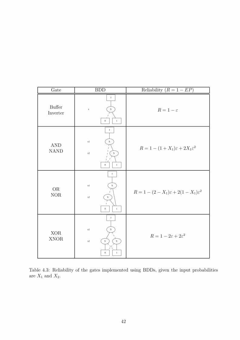
Gate BDD Reliability (R = 1− EP )
BufferInverter
x
f
S
0 1
R = 1− ε
ANDNAND
x1
x2
f
S
S
0 1
R = 1− (1 +X1)ε+ 2X1ε2
ORNOR
x1
x2
f
S
S
10
R = 1− (2−X1)ε+ 2(1−X1)ε2
XORXNOR
x1
x2
f
S
S S
0 1
R = 1− 2ε+ 2ε2
Table 4.3: Reliability of the gates implemented using BDDs, given the input probabilitiesare X1 and X2.
42

4.4.1 Input Error Probability and SNR
For simulation purposes, we add noise to the input signals (according to a certain SNR
value or noise power), simulate the circuit for a long simulation run, observe the outputs
and count the errors to obtain a reliability measure. The relationship between the input
error probability and the SNR of a Binary Non-Return to Zero (On-Off keyed) input signal
is given by [106]:
Pe = Q
(
d
2σ
)
(4.17)
where Q(x) = 12erfc( x√
2), and d is the separation between the ’1’ value and the ’0’ value.
The noise power is defined in terms of the noise power spectral density by the following
equation:
σ2 =No
2(4.18)
The average energy per bit is given as:
Eb =Ta
Ta + Tb
∫ Ta
0
V 2a dt+
TbTa + Tb
∫ Tb
0
V 2b dt
=V 2a T
2(4.19)
where Va is the amplitude of the ’1’ value, Vb is the amplitude of the ’0’ value. Here, we
assume Vb = 0 and T is the bit period such that Ta = Tb = T . Below, we will use a
normalized value for the bit period. Since Va is the separation between the ’1’ and ’0’ values,
then, in equation (4.17) the value of d is Va. Using equation (4.19), d =√2Eb. Substituting
it in equation (4.17) we obtain:
Pe = Q
( √2Eb
2√
No/2
)
= Q
(
√
Eb
No
)
(4.20)
The value Eb/No is equal to the SNRbit, which is the same as the SNR, if there is no
modulation or no combination of multiple bits per transmission symbol. To find the noise
43
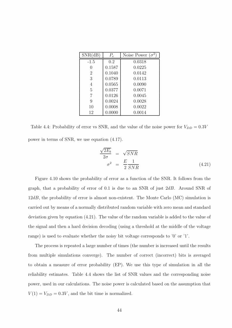
SNR(dB) Pe Noise Power (σ2)
-1.5 0.2 0.03180 0.1587 0.02252 0.1040 0.01423 0.0789 0.01134 0.0565 0.00905 0.0377 0.00717 0.0126 0.00459 0.0024 0.002810 0.0008 0.002212 0.0000 0.0014
Table 4.4: Probability of error vs SNR, and the value of the noise power for VDD = 0.3V
power in terms of SNR, we use equation (4.17).
√2Eb
2σ=
√SNR
σ2 =E
2
1
SNR(4.21)
Figure 4.10 shows the probability of error as a function of the SNR. It follows from the
graph, that a probability of error of 0.1 is due to an SNR of just 2dB. Around SNR of
12dB, the probability of error is almost non-existent. The Monte Carlo (MC) simulation is
carried out by means of a normally distributed random variable with zero mean and standard
deviation given by equation (4.21). The value of the random variable is added to the value of
the signal and then a hard decision decoding (using a threshold at the middle of the voltage
range) is used to evaluate whether the noisy bit voltage corresponds to ’0’ or ’1’.
The process is repeated a large number of times (the number is increased until the results
from multiple simulations converge). The number of correct (incorrect) bits is averaged
to obtain a measure of error probability (EP). We use this type of simulation in all the
reliability estimates. Table 4.4 shows the list of SNR values and the corresponding noise
power, used in our calculations. The noise power is calculated based on the assumption that
V (1) = VDD = 0.3V , and the bit time is normalized.
44

−2 0 2 4 6 8 10 1210
−4
10−3
10−2
10−1
100
Probability of Error vs SNR
SNR (dB)
Pe
Monte Carlotheory
Figure 4.10: Probability of Input error vs Input signal SNR
4.5 Error-correction coding
In this section, we investigate enhancing the circuit reliability via error correction. A block
code, denoted as (n, k) with n > k, consists of code words of length n digits that map to
a smaller set of words of k digits. The code rate is defined as kn, and is always less than
1. A block code is linear, if the modulo-2 sum of any two codewords is also a codeword.
The Hamming distance between two codewords is the number of digits in which they differ.
This can be used in either error detection, or error detection and correction, if the minimum
Hamming distance gives enough separation to determine which codeword is the most likely
one. If the minimum Hamming distance is 3, then it is possible to correct one error and detect
2 errors. Codewords are constructed using a generator matrix, and the original codeword is
restored after errors using a parity check matrix (see [87, 106]). The Hamming code is one
of the block codes that have a minimum Hamming distance of 3. For Hamming codes, the
number of parity bits is given as m and the code word length and message length are given
45
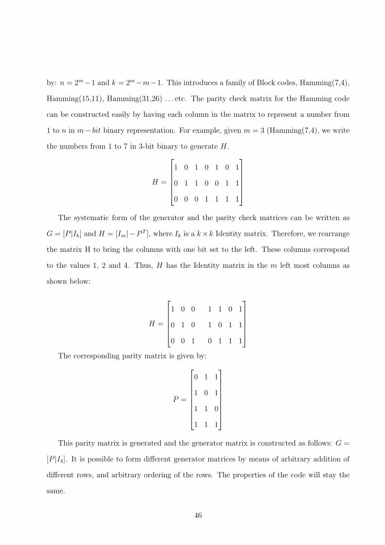
by: n = 2m−1 and k = 2m−m−1. This introduces a family of Block codes, Hamming(7,4),
Hamming(15,11), Hamming(31,26) . . . etc. The parity check matrix for the Hamming code
can be constructed easily by having each column in the matrix to represent a number from
1 to n in m− bit binary representation. For example, given m = 3 (Hamming(7,4), we write
the numbers from 1 to 7 in 3-bit binary to generate H .
H =
1 0 1 0 1 0 1
0 1 1 0 0 1 1
0 0 0 1 1 1 1
The systematic form of the generator and the parity check matrices can be written as
G = [P |Ik] and H = [Im|−P T ], where Ik is a k×k Identity matrix. Therefore, we rearrange
the matrix H to bring the columns with one bit set to the left. These columns correspond
to the values 1, 2 and 4. Thus, H has the Identity matrix in the m left most columns as
shown below:
H =
1 0 0 1 1 0 1
0 1 0 1 0 1 1
0 0 1 0 1 1 1
The corresponding parity matrix is given by:
P =
0 1 1
1 0 1
1 1 0
1 1 1
This parity matrix is generated and the generator matrix is constructed as follows: G =
[P |I4]. It is possible to form different generator matrices by means of arbitrary addition of
different rows, and arbitrary ordering of the rows. The properties of the code will stay the
same.
46

To generate a code word, we multiply a data word ”a” of k−bits by the generator matrix
as follows:
c = aG = [aP |a]
Therefore, a code word consists of parity bits (aP ), and the message bits a. This overhead
in the number of bits is linear, and the code rate r = k/n approaches 1 as both k and n
increase.
4.5.1 Shortened codes
The Hamming codes are defined in terms of the parity bits, such that the code is given as
(2m − 1, 2m − m − 1). For arbitrary message lengths, we can use the next higher value of
2m−m−1 as the message length, and encode all the extra bits as zeros. The position of the
extra zeros is arbitrary, and we can, thus, truncate any rows of choice in the parity matrix.
For example, if we want to define a Hamming code for a message of length k = 2, we start by
choosing the nearest Hamming code: Hamming(7,4). Next, we shorten the code by encoding
each message in the form [00a1a0], or [a1a000], or [0a1a00], or [a10a00]. This will effectively
remove two rows from the parity matrix making it P2×3. Two rows and two columns will
be removed from the generator matrix, where the identity matrix will lose two columns, so
that G = [P2×3|I2]. This way we obtain the code words of the shortened Hamming code
Hamming(5,2). This code is still capable of correcting only 1 error. The number of vectors
that the code can correct is 2k(1 + n). However, the number of vectors in the code space is
2n. This means that a shortened Hamming code is not a perfect code as it does not map
2n − 2k(1 + n) input vectors. In the case of the non-perfect Hamming(5,2), the number of
non-mapped vectors is 32 − 4 × 6 = 8. These non-mapped vectors can be dealt with by
assigning them to an error indicator or by assigning them to one of the nearest code words
according to the following definitions [87].
47

Definition 8 Amaximum-likelihood error-correcting decoder is a decoder that, given
the received word r, selects the code word c which minimizes the Hamming distance dH(r, c).
Definition 9 A bounded-distance error-correcting decoder is a decoder that can se-
lect the correct codeword, if the number of errors is dH(r, c) ≤ t. Otherwise, it signals the
decoder failure.
The maximum likelihood decoder uses a standard array to achieve complete decoding.
The standard array for the shortened code H(5, 2) with parity matrix [ 1 1 01 0 1 ] is shown in
Table 4.5. The standard array is constructed by writing the code words (n-bit 2k words) in
the first row. Then rows 2 to 6 in the first column, we have the least weight error vectors
(weight = 1). In rows 7 and 8 we put the next higher weight (weight = 2) error vectors. We
choose these particular vectors because the values in them are not any where in the rows 1
to 6. A bounded distance error-correcting decoder only uses rows 1 to 6 while a maximum
likelihood decoder uses the whole standard array that covers all the 2n possibilities. It can
decode any single bit error, or 2 patterns of double bit errors. The standard array for the
shortened code H(6, 3) with parity matrix [1 1 01 0 10 1 1
] is shown in table 4.6. The rows 2 to 7
in the first column, we have the least weight error vectors (weight = 1). The remaining
possibilities are 26 − 23(1 + 6) = 8 which is enough for only one extra row. The pattern in
the last row with double errors is again chosen based on uniqueness.
4.6 BDD model with error correction
Given a function f of k variables, its BDD includes k levels. If a switching error happens
at a BDD node, it cannot be corrected. The corresponding error-correcting BDD can be
designed as follows: a binary code (n, k) is constructed, and the function f is mapped into a
function f ′, which is implemented using another BDD with n levels [7]. Note that we are not
interested in mapping a code word c into an original message word a, but rather in mapping
48
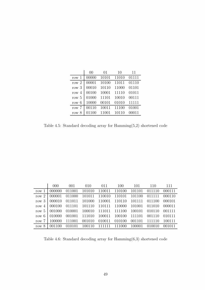
00 01 10 11row 1 00000 10101 11010 01111row 2 00001 10100 11011 01110row 3 00010 10110 11000 01101row 4 00100 10001 11110 01011row 5 01000 11101 10010 00111row 6 10000 00101 01010 11111row 7 00110 10011 11100 01001row 8 01100 11001 10110 00011
Table 4.5: Standard decoding array for Hamming(5,2) shortened code
000 001 010 011 100 101 110 111row 1 000000 011001 101010 110011 110100 101101 011110 000111row 2 000001 011000 101011 110010 110101 101100 011111 000110row 3 000010 011011 101000 110001 110110 101111 011100 000101row 4 000100 011101 101110 110111 110000 101001 011010 000011row 5 001000 010001 100010 111011 111100 100101 010110 001111row 6 010000 001001 111010 100011 100100 111101 001110 010111row 7 100000 111001 001010 010011 010100 001101 111110 100111row 8 001100 010101 100110 111111 111000 100001 010010 001011
Table 4.6: Standard decoding array for Hamming(6,3) shortened code
49

it to the target value of the binary function (c → f(a)). This means that no decoding is
required, and the code words are mapped to binary 0 or 1.
Applying the theory of block codes in this context is straight forward. Cyclic codes in
general have the advantage over block codes of easier encoding and decoding which is not
our target. Convolutional codes are suitable for continuous data streams and they target
retrieving the message. This is against the requirement that groups of binary messages
representing the function inputs are applied one at a time. There is also no direct relation
between BDDs and trellis decoders. Dealing with input streams, would require a new type
of decoder that generates a corresponding correct output stream. It will not be a BDD, but
a trellis decoder.
Hamming codes are a subset of block codes and they have the desired property of cor-
recting a single error using the minimum number of extra parity bits. They are suitable for
small binary messages with minimum coding overhead. In this study, Hamming codes are
used. This means that the new BDD will be able to withstand a single decision error due
to signal noise. In an ordered BDD composed of branches, only one branch is used a time.
A variable appears on a branch only once. A branch will have just one node controlled by
this input variable and, therefore, error in all other branches is irrelevant. The fault model
assumes that the errors in the inputs are independent. This is not realistic, if the error is
caused by noise which may affect the closely packed levels of nodes. It is realistic, if the
source of error is the switching node itself when an electron would tunnel across the wrong
barrier in a wrap gate device due to manufacturing tolerance and temperature sensitivity.
The probability, that this would happen in more than one gate in a branch simultaneously,
is assumed to be low.
A shortened Hamming code will be used in the case of an arbitrary number of inputs
that cannot be written as 2m−m− 1. With shortened codes, a number of input vectors will
have an undefined target as we mentioned earlier. We choose to map these vectors to the
50

binary value ’0’, and optionally have an extra error indicator as shown in Figure 4.11.
x1
p0
p1
p2
x2
f Unmapped
S S
SS
SS
S
S
S S
SS
1
S
0
SS
Figure 4.11: Error-correcting NAND gate BDD with indicator for unmapped vector values.
Consider the implementation of a Buffer gate, using a one-level decision diagram. This
function of one variable corresponds to the (3, 1) error-correcting code, in which 0 is encoded
by 000, and one is encoded by 111. The decoder of such code represents a majority-vote
function: it decodes the received codewords 000, 001, 010 and 100 as 0.
A generic 2 input binary function augmented with parity bits using the code (5,2) is
shown in Figure 4.12 as a diagram with multiple values in the terminal nodes. The value ’E ’
represents the error value for the non-mapped vectors in the shortened code. This decision
diagram can be the basis for generating the error-correcting binary decision diagram of any
elementary gate by replacing the terminal nodes with the values ’0’ and ’1’ and merging the
diagram nodes accordingly. Generation of the parity bits is done by multiplying the message
bits by the parity matrix (aP ), using modulo-2 addition. Since this operation is exclusively
51

binary, we can use a BDD to generate the parity bits from the message bits instead of
explicitly carrying out the matrix multiplication. For the shortened code (5,2), the parity
generation diagram is shown in Figure 4.13 for a parity matrix given as P =(
1 1 01 0 1
)
.
Figure 4.12: An error-correcting multi-valued decision diagram for a generic 2-input func-tions. In binary representation, the values of the terminal nodes are 0 or 1, and the nodesare merged accordingly.
Table 4.7 illustrates the error-correcting diagrams of the elementary gates. To generate
the diagrams in this table, we used a custom tool that can be downloaded from the author’s
website1. The tool uses a slightly modified CUDD package [126]. The modifications are
in the output functions; dumpDot and dumpBlif . The first modification is to optionally
change the node labels in the dot file from hexadecimal numbers to a literal constant, which
is more appealing visually. The original dumpBlif function does not output the correct
input variable order, if variable reordering has been called. Since the output blif is used to
construct the structure of the BDD in memory for planarization, and in order to simplify the
code so that it does not require a separate variable order file, the modification was made.
1http://people.ucalgary.ca/~tsemoham/bdd
52

x1
x2
p2 p1
S
p0
S
SS
01
Figure 4.13: A parity bit generator for the shortened Hamming(5,2).
The upper limit on complexity with block codes is doubling the number of the circuit
elements while achieving the coding gain. The doubling is an upper limit based on the
code rate which approaches 1/2 when the message length is very large according to the
reference [105].
The increase in the BDD size will be of linear complexity. In the worst case, however,
the unreduced BDD has a size that is exponential in the number of variables. Augmenting
the function variables by the parity bits will result in an exponential increase in complexity,
unless function decomposition is considered. Consider the error-correcting diagram of a 2-
bit adder implemented using the standard Hamming(7,4) shown in Figure 4.14. The adder
adds the 2 binary words a1a0 and b1b0. The original shared diagram has 11 nodes, while the
error-correcting shared diagram has 61 nodes. Another alternative is to replace each node
by 4 nodes, representing the noise tolerant diagram of the buffer/inverter circuit, then the
number of nodes is 4 × nnodes. However, the number of diagram levels becomes 3 × k. The
block coding theory, however, tells us that repeating each bit n-times is inferior to block
coding. In the next section, we will elaborate further on this statement.
53

Gate BDD Errorcorrecting BDD
Buffer/Inverter x
f
S
0 1
p0
p1
x
f
S
S S
S
1 0
AND
x1
x2
f
S
S
0 1
p1
p0
x1
p2
x2
f
S
S S
S
0
S
S S
S
1
OR
x1
x2
f
S
S
10
x1
p1
p0
p2
x2
f
S
SS
S
1
S
SSS
SS
0
54
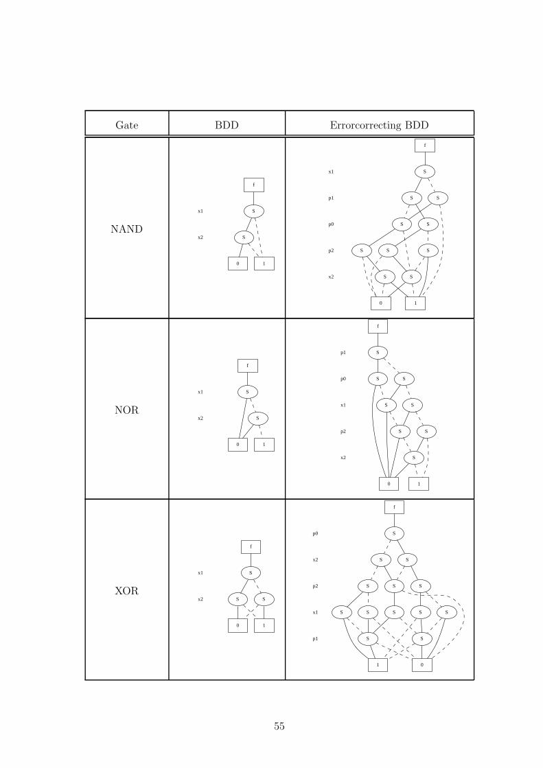
Gate BDD Errorcorrecting BDD
NAND
x1
x2
f
S
S
10
x1
p1
p0
p2
x2
f
S
SS
S
1
S
SSS
SS
0
NOR
x1
x2
f
S
S
0 1
p1
p0
x1
p2
x2
f
S
S S
S
0
S
SS
S
1
XOR
x1
x2
f
S
S S
0 1
p0
x2
p2
x1
p1
f
S
S S
S S S
SS SSS
0
S
1
S
55
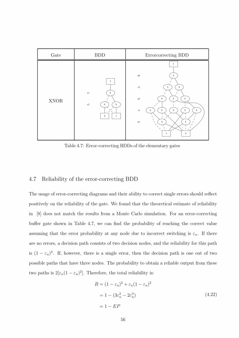
Gate BDD Errorcorrecting BDD
XNOR
x1
x2
f
S
S S
0 1
p0
x2
p2
x1
p1
f
S
SS
S SS
S
0
SS SS
SS
1
Table 4.7: Error-correcting BDDs of the elementary gates
4.7 Reliability of the error-correcting BDD
The usage of error-correcting diagrams and their ability to correct single errors should reflect
positively on the reliability of the gate. We found that the theoretical estimate of reliability
in [8] does not match the results from a Monte Carlo simulation. For an error-correcting
buffer gate shown in Table 4.7, we can find the probability of reaching the correct value
assuming that the error probability at any node due to incorrect switching is εn. If there
are no errors, a decision path consists of two decision nodes, and the reliability for this path
is (1 − εn)2. If, however, there is a single error, then the decision path is one out of two
possible paths that have three nodes. The probability to obtain a reliable output from these
two paths is 2[εn(1− εn)2]. Therefore, the total reliability is:
R = (1− εn)2 + εn(1− εn)
2
= 1− (3ε2n − 2ε3n)
= 1− EP
(4.22)
56

a1
p1
p2
b1
p0
b0
a0
s2 s1
S
s0
S
SS S S S
SS S S S SSS SS
S S SS SSS S S SSSS S SS SS
S SS
S
SS S
1
SSS
0
S
S
SSS
S
S
S
SS SS SSS
S SS S S
S
S
S
Figu
re4.14:
Error-correctin
g2x
2bitad
der.
57
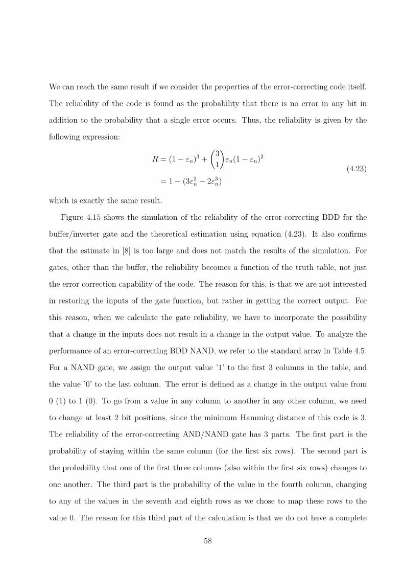
We can reach the same result if we consider the properties of the error-correcting code itself.
The reliability of the code is found as the probability that there is no error in any bit in
addition to the probability that a single error occurs. Thus, the reliability is given by the
following expression:
R = (1− εn)3 +
(
3
1
)
εn(1− εn)2
= 1− (3ε2n − 2ε3n)
(4.23)
which is exactly the same result.
Figure 4.15 shows the simulation of the reliability of the error-correcting BDD for the
buffer/inverter gate and the theoretical estimation using equation (4.23). It also confirms
that the estimate in [8] is too large and does not match the results of the simulation. For
gates, other than the buffer, the reliability becomes a function of the truth table, not just
the error correction capability of the code. The reason for this, is that we are not interested
in restoring the inputs of the gate function, but rather in getting the correct output. For
this reason, when we calculate the gate reliability, we have to incorporate the possibility
that a change in the inputs does not result in a change in the output value. To analyze the
performance of an error-correcting BDD NAND, we refer to the standard array in Table 4.5.
For a NAND gate, we assign the output value ’1’ to the first 3 columns in the table, and
the value ’0’ to the last column. The error is defined as a change in the output value from
0 (1) to 1 (0). To go from a value in any column to another in any other column, we need
to change at least 2 bit positions, since the minimum Hamming distance of this code is 3.
The reliability of the error-correcting AND/NAND gate has 3 parts. The first part is the
probability of staying within the same column (for the first six rows). The second part is
the probability that one of the first three columns (also within the first six rows) changes to
one another. The third part is the probability of the value in the fourth column, changing
to any of the values in the seventh and eighth rows as we chose to map these rows to the
value 0. The reason for this third part of the calculation is that we do not have a complete
58

mapping. In incomplete mapping (bounded-distance error-correcting decoder), we assume
that the unmapped control signal sequence (data + parity) results in always choosing a
path to the ’0’ terminal node. Otherwise, with complete mapping, there is no need to have
a distinction between rows in the table. One alternative is to have an extra terminal node
(’E’) in the diagram to represent the unmapped sequence as shown in Figure 4.12. The other
alternative is to have an extra root node to indicate decoder failure as shown in Figure 4.11.
REC NAND = REC +1
2(R00↔01 +R00↔10) +
1
2R10↔01 +
1
4Runmapped
= (1− εn)5 + 5εn(1− εn)
4
+3
4(3ε3n(1− εn)
2 + 6ε2n(1− εn)3 + 3ε4n(1− εn))
+1
4(ε2n(1− εn)
3)
(4.24)
It must be emphasized that the derivation of the reliability in equation (4.24) does not take
into account the structure of the diagram itself, but only the properties of error-correction
coding, in conjunction with the truth table of the gate.
Figure 4.17 illustrates the theoretical value of the reliability from equation (4.24) and
the result of a Monte Carlo (MC) simulation of the error-correcting decision diagram. The
simulation is carried out by means of random errors applied independently at each of the
signal levels. Figure 4.17 also compares this result to the effect of replacing each node of
the NAND BDD by an error-correcting BDD node based on the TMR buffer/inverter. This
means that each node in the original BDD of a gate is simply replaced by an error-correcting
node (composed internally of 4 nodes) such as the one shown in Figure 4.16. This means we
will have 6 signal levels and 4× 2 = 8 nodes for the TMR NAND as opposed to 10 nodes in
the EC NAND and 5 levels. Again, for the MC simulation, we apply independent noise at
each of the 6 levels. The reliability of the error-correcting XOR gate is shown in Figure 4.18.
For a 2-bit adder, the original BDD has 3 outputs and 11 nodes, the TMR adder has 44
nodes and the Hamming code adder has 61 nodes. The reliability performance simulation of
59

0 0.1 0.2 0.3 0.4 0.5
0.4
0.5
0.6
0.7
0.8
0.9
1Reliability of EC buffer/inverter
Probability of Error
Rel
iabi
lity
Monte Carlo SimulationTheoretical EstimateNon−ECAstola’s estimate
Figure 4.15: Reliability of the error-correcting BDD for the buffer/inverter
each of them is shown in Figure 4.19 for each of the individual outputs s2s1s0 of the adder.
The results show that the performance with error coding is better than the original BDD
circuit. It should be noted that for s2 and s0, the TMR performance is superior. However,
it is not possible to consider individual results because the diagram is shared and can be of
only one type, either TMR or Hamming code based. The overall performance is shown in
Figure 4.20 as the average reliability performance over the all the outputs. It shows that the
overall performance is comparable.
4.8 Experiments
Several simulation models for the switching node in a BDD can be considered as in Figure 4.2.
A high-level simulation using VHDL utilizes the multiplexer model of a node. The results
obtained in the previous section for reliability, used this high-level abstract model, which
only models the node as an ideal selection switch. This ideal model is used to simulate
60

S
S
S S
S
Figure 4.16: An error-correcting BDD node used in TMR simulations
0 0.05 0.1 0.15 0.2 0.25 0.3 0.35 0.4 0.45 0.50.4
0.5
0.6
0.7
0.8
0.9
1Reliability of EC NAND gate
Probability of Error
Rel
iabi
lity
MC HammingTheoretical EstimateMC TMRNon−EC
Figure 4.17: Reliability of the error-correcting BDD for the AND/NAND gate
61
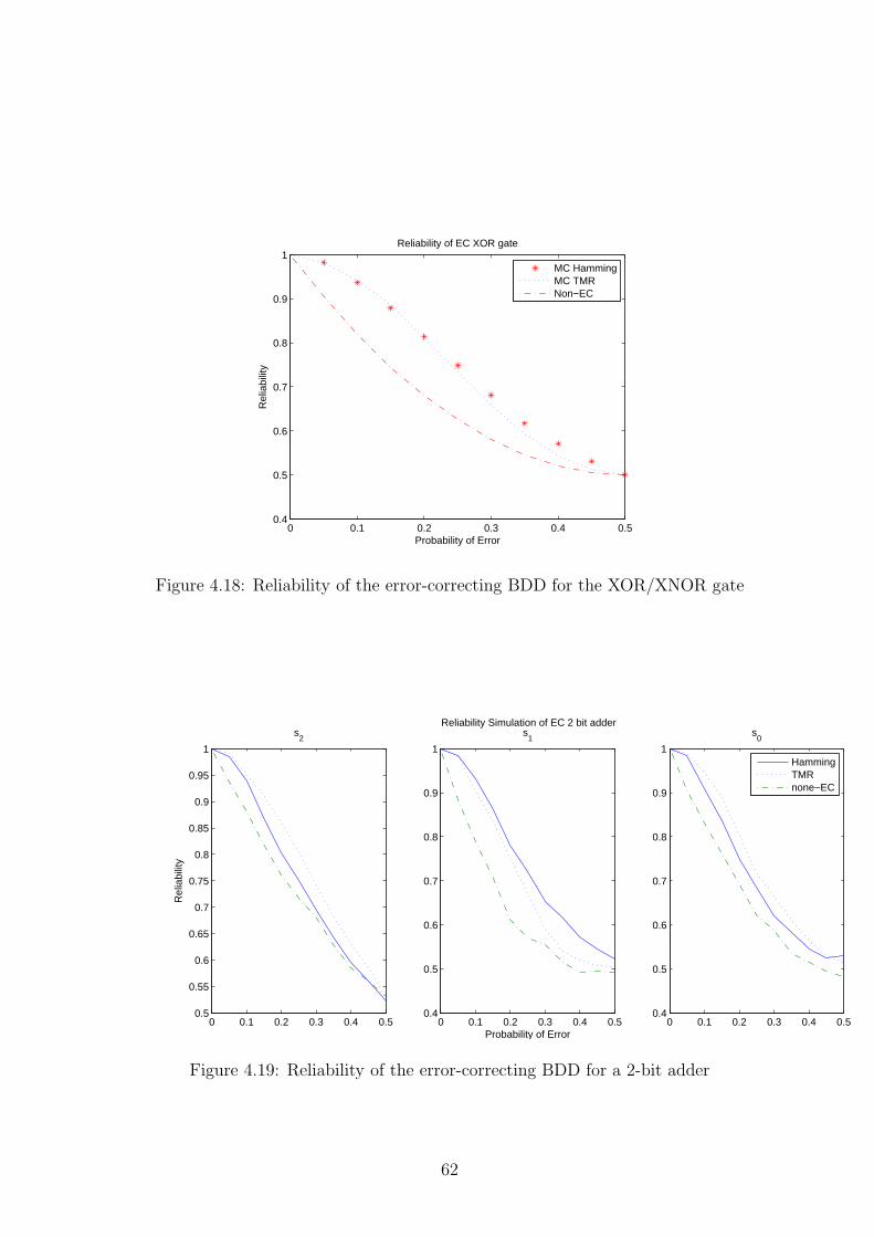
0 0.1 0.2 0.3 0.4 0.50.4
0.5
0.6
0.7
0.8
0.9
1Reliability of EC XOR gate
Probability of Error
Rel
iabi
lity
MC HammingMC TMRNon−EC
Figure 4.18: Reliability of the error-correcting BDD for the XOR/XNOR gate
0 0.1 0.2 0.3 0.4 0.50.5
0.55
0.6
0.65
0.7
0.75
0.8
0.85
0.9
0.95
1
s2
Rel
iabi
lity
0 0.1 0.2 0.3 0.4 0.50.4
0.5
0.6
0.7
0.8
0.9
1
Reliability Simulation of EC 2 bit adders
1
Probability of Error0 0.1 0.2 0.3 0.4 0.5
0.4
0.5
0.6
0.7
0.8
0.9
1
s0
HammingTMRnone−EC
Figure 4.19: Reliability of the error-correcting BDD for a 2-bit adder
62

0 0.1 0.2 0.3 0.4 0.50.5
0.55
0.6
0.65
0.7
0.75
0.8
0.85
0.9
0.95
1
Probability of Error
Average Reliability of EC 2 bit adder
HammingTMRnone−EC
Figure 4.20: Average reliability of the error-correcting BDD for a 2-bit adder
the performance of a 2-bit adder and assess the bit-error rate averaged over the 3 adder
outputs as the SNR is degraded. An instance of the simulation at SNR = 9dB is shown
in Figure 4.22, and results for other SNR values are given in Table 4.8. The point of this
simulation is to illustrate that error-correction allows one to achieve almost an order of
magnitude of performance enhancement.
To model circuit delays, we may use the simplified bidirectional hysteresis switch cir-
cuit model to find the results in less simulation time. This is important for large circuits
when running the simulation using the complete set of model parameters requires a long
time. In the simulation experiments, we use the dual transmission gate representation of the
switching node (2 pairs of pass-transistors) along with LP 16nm predictive CMOS technol-
ogy model from [134]. The simulator used is Ngspice [90], which has a feature that allows
adding noise on the control signals. The noise mean is zero, and the standard deviation is
calculated from equation (4.21). The circuit description is automatically generated based
on the diagram. Table 4.8 shows a comparison between the error correcting version of the
NAND gate implemented as a BDD and other implementations simulated using the same
63

0 0.5 1 1.5 2 2.5
x 10−7
−0.5
0
0.5
1
1.5
2
2.5
3
3.5
4
time (s)
Vol
tage
(V
)Spice simulation of EC/TMR buffer circuit at SNR=3dB
p1p0aoutput
Figure 4.21: Spice simulation of EC buffer with different random noise applied at each level.
predictive 16nm technology. The gate voltage in the simulations is above threshold and is
set to VDD. Figure 4.21 shows how the transistor-level circuit handles large superimposed
noise at all the switching levels.
uncorrected Error correctionSNR BER BER3 0.4126 0.16505 0.3236 0.08717 0.2080 0.02839 0.0933 0.005210 0.0510 0.001612 0.0107 0
Table 4.8: Noise tolerance in error-correcting 2x2 bit adder with uncorrelated noise addedat all 4 inputs for various SNR levels
64

500 1000 1500 2000 2500 3000 3500
0
5
10
15SNR=9dB, original ber=0.092617
Number of bits
Out
puts
(s0,s
1,s2)
Inpu
ts(b
0,b1,a
0,a1)
(a)
500 1000 1500 2000 2500 3000 3500
0
5
10
15SNR=9dB, error correction ber=0.0049
Number of bits
Out
puts
(s0,s
1,s2)
Inpu
ts(b
0,b1,a
0,a1)
(b)
Figure 4.22: (a)Simulation of the 2x2 adder without error-correction at SNR = 9dB.(b)Simulation of the adder with error-correction. BER values are averaged for all 3 out-put bits.
65
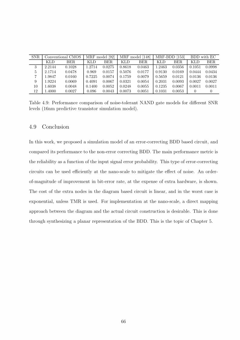
SNR Conventional CMOS MRF model [92] MRF model [148] MRF-BDD [153] BDD with ECKLD BER KLD BER KLD BER KLD BER KLD BER
3 2.2144 0.1028 1.2714 0.0275 0.8618 0.0463 1.2463 0.0356 0.1051 0.09985 2.1714 0.0478 0.969 0.0157 0.5076 0.0177 0.9130 0.0169 0.0444 0.04347 1.9847 0.0160 0.7225 0.0074 0.1759 0.0079 0.5659 0.0121 0.0136 0.01369 1.9224 0.0069 0.4091 0.0067 0.0321 0.0054 0.2031 0.0093 0.0027 0.002710 1.6038 0.0048 0.1400 0.0052 0.0248 0.0055 0.1235 0.0067 0.0011 0.001112 1.4000 0.0027 0.096 0.0043 0.0073 0.0051 0.1031 0.0053 0 0
Table 4.9: Performance comparison of noise-tolerant NAND gate models for different SNRlevels (16nm predictive transistor simulation model).
4.9 Conclusion
In this work, we proposed a simulation model of an error-correcting BDD based circuit, and
compared its performance to the non-error correcting BDD. The main performance metric is
the reliability as a function of the input signal error probability. This type of error-correcting
circuits can be used efficiently at the nano-scale to mitigate the effect of noise. An order-
of-magnitude of improvement in bit-error rate, at the expense of extra hardware, is shown.
The cost of the extra nodes in the diagram based circuit is linear, and in the worst case is
exponential, unless TMR is used. For implementation at the nano-scale, a direct mapping
approach between the diagram and the actual circuit construction is desirable. This is done
through synthesizing a planar representation of the BDD. This is the topic of Chapter 5.
66

Chapter 5
Synthesis of Planar Nano-Circuits
5.1 Introduction
Planar diagrams have the advantage that they can be directly mapped to the device level
without any effort in placement and routing. Interconnections are always short and local.
Thus, timing and area estimates are accurate and the design constraints can be easily sat-
isfied. They are also an important requirement in circuits built using nanowire wrap gate
devices proposed in [49,60]. They have the disadvantage that their structure increases expo-
nentially in size and in one direction only. For large diagrams, circuit decomposition is often
necessary because of the exponential increase in size and the signal degradation as it crosses
multiple switching levels specially in a pass-transistor logic implementation. Processing a
node graph is an NP-hard problem because it requires the consideration of all possible com-
binations of all the nodes. There are several approaches to this problem in the literature [72].
In [117], the authors address the planarization of multiple-valued logic diagrams and they
investigate specific types of functions; symmetric and monotonic functions; that can lead to
regular layouts. Such planar diagrams cannot be designed for arbitrary functions. In [88],
the authors synthesize regular triangular structures by means of repeating the control vari-
ables across multiple levels. In the work by Perkowski et al., the authors synthesize regular
lattice structures using various expansion types, namely the Shanon type, positive Davio
and negative Davio expansions [25, 99–102]. The resulting lattice diagrams are triangular.
They are not composed of simple decision nodes, but rather of complex unit cells.
In the decision diagram called YADD (Yet another decision diagram), triangular diagrams
are also generated, but the unit cell is a simple BDD multiplexer node [88]. The control
signals, however, have to be repeated across multiple levels. This affects the area and power
67

requirements. Delays in signal propagation between levels are dealt with by pipelining the
control signals.
In [21], the authors describe a technique to eliminate crossings in QCA layouts. In this
case, the circuit is not hierarchical nor arranged into levels as in BDDs, and the goal is to
remove edge crossings by means of a crossing elimination algorithm.
In this chapter, we describe two algorithms for the generation of planar binary decision
diagram that assume only one type of nodes and requires no repetition of the control signal
levels. This can be achieved by the insertion of dummy nodes, node swapping, node dupli-
cation, control signal duplication [18, 19]. Dummy nodes are just routing nodes that have
no logic functionality. They are used to meet the planarization algorithm requirement that
parent nodes and child nodes are always in adjacent levels. The first algorithm has linear
time complexity with respect to the number of the nodes while the second algorithm has
exponential time complexity. While the second algorithm achieves better results in general,
its exponential time requirement may render it prohibitive for analyzing large diagrams that
have 10 input control variables or more. Heuristics are used to search for a solution within a
given set instead of evaluating all possibilities to find the best solution. The generated planar
diagrams are not canonical nor optimum. To find an optimal planar diagram, its nodes in all
the signal levels must be considered. The results reported in [18] are questionable, because
the reported results show a linear time performance for all circuits, regardless of their size
despite arguing otherwise. Also, the number of nodes reported is either too small or too
large for some circuits. This was verified by running the two algorithms on the same circuits
and tabulating the results. The results reported in [21] cannot be verified because they are
based on multiple tools that are not available. In this thesis work, we developed a tool1 that
can also handle the planarization of BDDs that have complemented edges.
Two examples for a planarized error correcting BDD of a NAND gate and the s2 output
1See Appendix A for more details.The tool is available for download at http://people.ucalgary.ca/~tsemoham/bdd
68
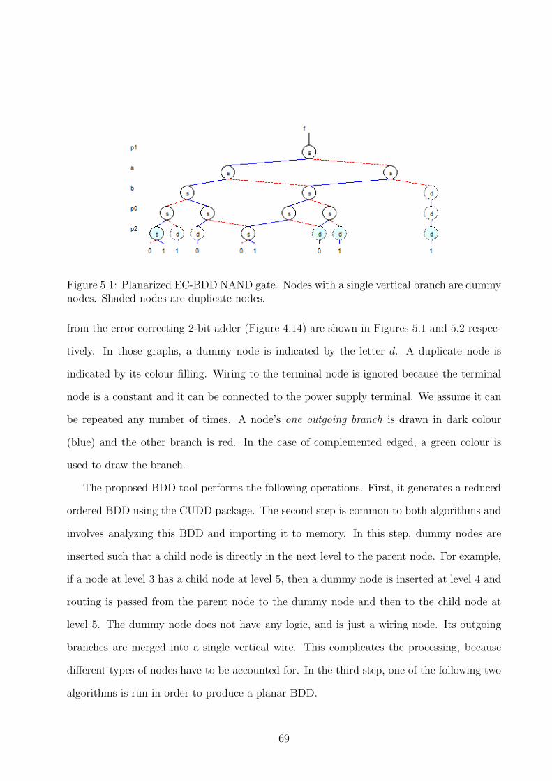
Figure 5.1: Planarized EC-BDD NAND gate. Nodes with a single vertical branch are dummynodes. Shaded nodes are duplicate nodes.
from the error correcting 2-bit adder (Figure 4.14) are shown in Figures 5.1 and 5.2 respec-
tively. In those graphs, a dummy node is indicated by the letter d. A duplicate node is
indicated by its colour filling. Wiring to the terminal node is ignored because the terminal
node is a constant and it can be connected to the power supply terminal. We assume it can
be repeated any number of times. A node’s one outgoing branch is drawn in dark colour
(blue) and the other branch is red. In the case of complemented edged, a green colour is
used to draw the branch.
The proposed BDD tool performs the following operations. First, it generates a reduced
ordered BDD using the CUDD package. The second step is common to both algorithms and
involves analyzing this BDD and importing it to memory. In this step, dummy nodes are
inserted such that a child node is directly in the next level to the parent node. For example,
if a node at level 3 has a child node at level 5, then a dummy node is inserted at level 4 and
routing is passed from the parent node to the dummy node and then to the child node at
level 5. The dummy node does not have any logic, and is just a wiring node. Its outgoing
branches are merged into a single vertical wire. This complicates the processing, because
different types of nodes have to be accounted for. In the third step, one of the following two
algorithms is run in order to produce a planar BDD.
69

Figure 5.2: Planarized BDD implementing the output s2 of the EC-BDD 2-bit adder
70

5.2 Algorithm 1: Linear-time node processing
The algorithm carries out the generation of planar error-correcting diagrams by examining
the nodes of the diagram, one level at a time. At each level, nodes are arranged according
to the position of their parent nodes. We always assume that the parent nodes have fixed
positions within a level (locked in place) and cannot be moved or duplicated. There are 3
possible scenarios when only adjacent parent nodes are processed.
The first scenario shown in Figure 5.3 assumes that there are no common child nodes
between the nodes Sk and Sk+1 where k is the loop variable for the parent-node level. In
this case, the child nodes of each parent node are arranged according to the position of their
respective parent nodes. The choice whether to place a child node to the left or to the right
of the parent node is arbitrary. If a node has more than one parent and the parents are
not adjacent in position then this node is duplicated. We lock the children of the node Sk
in place so that they cannot be moved by a future operation. A possible future operation
involves the same child node but with a parent far away. In this case the parent would see
its child its locked in place and request a duplicate. In the next loop iteration, the nodes
Sk+1 and Sk+2 are considered.
In the second scenario shown in Figure 5.4, there is a one common child for the parent
nodes. In this case, the child is simply placed in the middle and locked in place. The other
children are placed to the right of the right parent node and to the left of the left parent
node. They are also locked in place. We then increment the loop variable twice, such that
the next parent nodes to consider are Sk+2 and Sk+3.
In the third scenario shown in Figure 5.5, two adjacent parents share two child nodes. In
this case, we arbitrarily choose a child node and place it in a middle position with respect
to the positions of the parent nodes. We duplicate the other child node and place it to the
right and to the left of the parents as before. We lock all these child nodes in place and
increment the loop variable twice such that the next parent nodes to consider are Sk+2 and
71
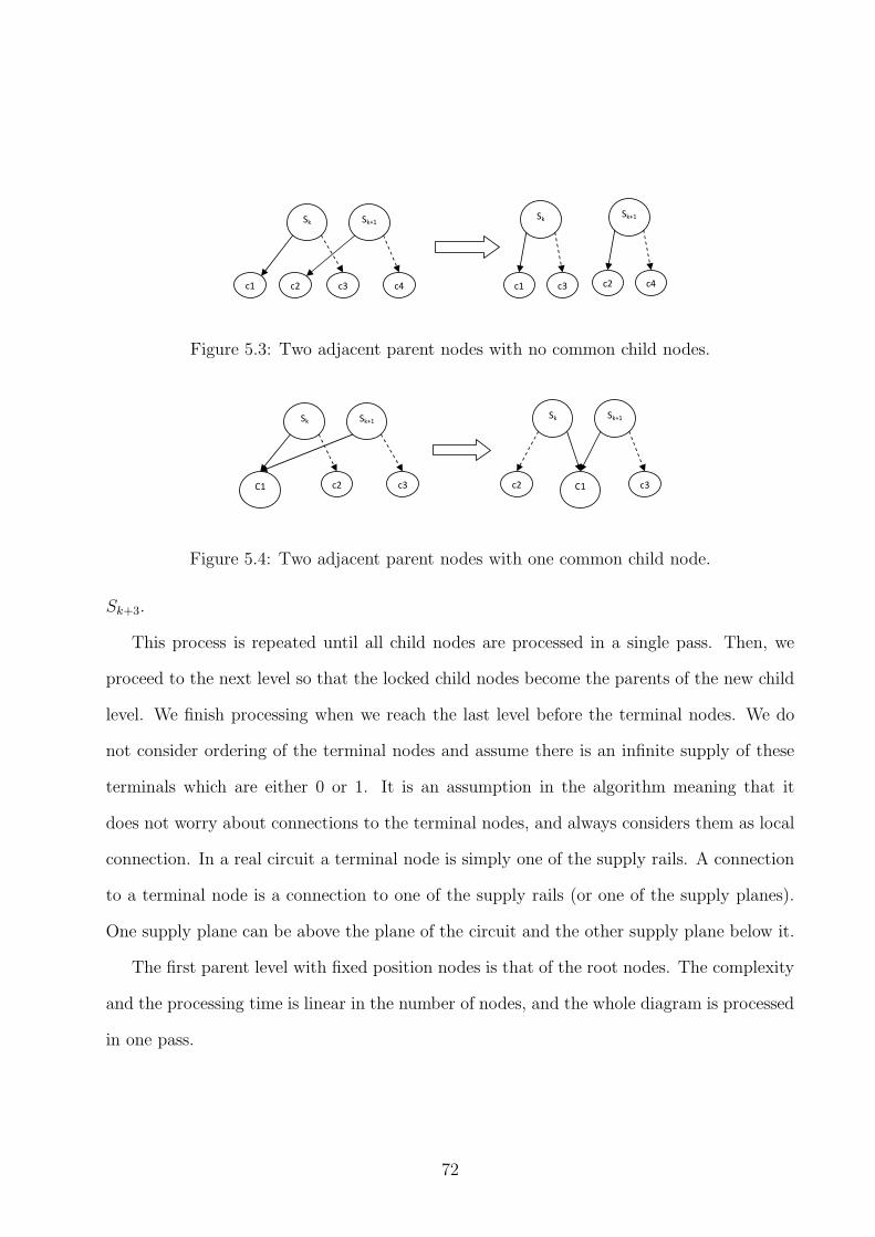
Figure 5.3: Two adjacent parent nodes with no common child nodes.
Figure 5.4: Two adjacent parent nodes with one common child node.
Sk+3.
This process is repeated until all child nodes are processed in a single pass. Then, we
proceed to the next level so that the locked child nodes become the parents of the new child
level. We finish processing when we reach the last level before the terminal nodes. We do
not consider ordering of the terminal nodes and assume there is an infinite supply of these
terminals which are either 0 or 1. It is an assumption in the algorithm meaning that it
does not worry about connections to the terminal nodes, and always considers them as local
connection. In a real circuit a terminal node is simply one of the supply rails. A connection
to a terminal node is a connection to one of the supply rails (or one of the supply planes).
One supply plane can be above the plane of the circuit and the other supply plane below it.
The first parent level with fixed position nodes is that of the root nodes. The complexity
and the processing time is linear in the number of nodes, and the whole diagram is processed
in one pass.
72

Figure 5.5: Two adjacent parent nodes with two common child nodes.
5.3 Algorithm 2: Multi-pass diagram processing
In order to maximize node sharing, parent nodes can be shuffled if their order is arbitrary.
This shuffling is repeated until the optimum number of node sharing is achieved. This can
lead to exponential time requirement and is best illustrated by the example in Figure 5.6.
In this case we run the same way as in the first algorithm but we keep track of the arbitrary
selections we make in the first scenario when there are no common nodes. In this case the two
children are labelled as coupled nodes. Coupled nodes, albeit locked in place, can exchange
their positions if this would result in a smaller number of duplicated nodes. Two coupled
nodes have four children which can be similarly coupled. In Figure 5.6, we show four levels
in which coupled nodes are found on the first three. In the fourth level, however, we show
only one common child node. In order to achieve minimum node duplication, we need to
rearrange the nodes in level 3. In this case we are considering rearranging the parent nodes
if they are couple nodes. The rearrangement is not only that two coupled nodes exchange
their places, but also the whole couple can exchange their place with an adjacent couple if
their parents are also coupled. This means that we keep back tracking upwards until we no
longer see coupled nodes. For the case in the example, the parent node shuffling will move
the two groups in level 3 that share a common child to the middle. Also the nodes in these
two groups will be uncoupled because a lone child has been located. Then the algorithm
will backtrack again upwards through all the levels of the involved parents and lock them in
place and uncouple them.
73
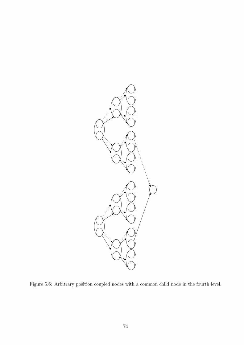
Figure 5.6: Arbitrary position coupled nodes with a common child node in the fourth level.
74

There is no guarantee how often this operation will have to be repeated. The method
used to find the required shuffling involves that, when we process a child level, we have to
iterate through all the possible arrangements of the parent nodes and keep a minimum score
that identifies a certain arrangement. This arrangement is then kept, and we proceed to the
next child level. The number of possible arrangements increases exponentially as more deep
levels of coupled nodes are generated. The final solution may not require that certain parent
nodes to be uncoupled and, thus, the final solution is arbitrary. The exponential increase
of parent position possibility is responsible for the exponential increase in time requirement
by the algorithm. When it is too large, the tool is instructed to pick some possible parent-
location combinations randomly and then choose the best one and proceed to the next level.
Otherwise, the run time is prohibitively too large for large circuits as shown in the results
section.
5.4 Results
We implemented both algorithms for multiple MCNC benchmark circuits as well as using
our own error correcting BDDs proposed in the previous chapter. The run time for each
algorithm is calculated by averaging the time for 10 consecutive runs. The fluctuation in the
measured run-time used is mainly due to caching and to the CLI garbage collector kicking
in while the algorithm is running. When the run-time reaches several hours, it is calculated
only once. The C880 benchmark was not tested with the second algorithm because of its
very large size, especially after the insertion of dummy nodes. This suggests incorporating
function decomposition before attempting to generate planar layouts. The results show that
for small circuits, the run time of the second algorithm is acceptable. The reduction in
the number of duplicate nodes is around 35% on average for larger circuits. Table 5.1 also
shows the results for different variable re-orderings. We tested exact and SIFT reordering.
Although, exact reordering, in general, is guaranteed to produce the least number of nodes
75

in a BDD, this advantage is not carried over when planarization is performed. A significant
effect of the variable reordering is apparent in some circuits like misex3.
Benchmark #inputs #outputs #nodes A1 #nodes A1 time A2 #nodes A2 time
ECadder(exact) 7 3 61 +77 0.6 ms +59 413 msECadder 7 3 68 +58 0.6 ms +53 44 ms9sym 9 1 33 +36 0.1 ms +16 27 ms
cm138a 6 8 17 +11 0.2 ms +11 16 msrd73 7 3 43 +73 6.5 ms +34 30.24 msalu2 10 6 188 +245 15.2 ms +185 19.47 s
apex4(exact) 9 19 970 +2204 153 ms +1919 72.18 sapex4 9 19 988 +2094 137 ms +1875 34.92 min
misex3(exact) 14 14 545 +3977 317 ms +2760 10 minmisex3 14 14 672 +2248 150 ms +1824 32.37 salu4 14 8 859 +2587 283 ms +1852 17.73 min
alu4(exact) 14 8 699 +1112 79 ms +1005 2 minC880 60 26 7090 +837219 12.85 Hr — —
Table 5.1: Planarization results (variable ordering is performed using SIFT algorithm unlessthe exact ordering (denoted (exact)) is used)
5.5 Conclusions
In this chapter, we introduced two algorithms for the generation of BDDs with planar layout.
The algorithms are implemented in a form of a software tool2 and the results for both algo-
rithms are analyzed. In both algorithms, the number of levels of the planarized BDD is equal
to the number of levels in the original BDD. Dummy nodes are inserted such that routing
is only necessary between adjacent levels. For the first algorithm, linear time processing
is guaranteed at the expense of increased number of duplicate nodes in each level. In the
second algorithm, the software keeps track of all possible combinations of node placements
and examines them all to minimize the number of duplicate nodes at a certain level. If more
than one combination have the same minimum score for node duplicates, they are kept for
further consideration using information from deeper levels. This may lead to exponential
2http://people.ucalgary.ca/~tsemoham/bdd
76

time requirement in the worst case. The benefit of reduction in the number of duplicted
nodes using the second algorithm is estimated at 35% on average.
77

Chapter 6
Crossbar Latch-based Combinational and Sequential
Logic for nano FPGA
6.1 Introduction
Molecular devices can exhibit desirable current-voltage (I-V) characteristics which makes
them possible candidates to replace conventional CMOS devices. Molecular devices require
a much lower footprint than CMOS transistors and therefore provide packing density capa-
bilities that would allow the continuation of the trend set by Moore’s law [23, 30, 128].
Using assemblies of nanowires and molecular devices, it is possible to implement simple
logic gates, digital computation and simple memories [89]. Although the fabrication of
working molecular scale devices has been successful, it is necessary to develop techniques
to integrate these devices to form large scale digital circuits with densities that surpass the
densities attained by common lithographic techniques and transistor scaling.
Previous work focused on using the crossbar array to implement programmable logic
arrays in which hybrid CMOS/nano approaches rely on lithographic scale electronics for
signal restoration and inversion. In this chapter, the crossbar latch, which is an integral part
of the crossbar array, is used to model full combinational logic circuits with signal restoration
and inversion. Nano architectures of primary combinational and sequential building blocks
are presented since they constitute the basis of a homogeneously structured nano processor
or nano FPGA.
The proposed nano system is assumed to interact with lithographic (microscale) devices
only for programming and signal I/O.
78

6.2 Device modeling
Designing electronic circuits with molecular devices entails the consideration of several key
issues. The first issue is concerned with obtaining device models that can be used to simulate
circuits built using the new devices. The device models are usually based on categorizing the
measured behaviour of molecular devices. The most prominent category is the programmable
resistor and the programmable rectifier device. These devices exhibit orders of magnitude
difference in conductivity between their programmed ’ON’ and ’OFF’ states and are thus
suitable for implementing digital circuits. The devices can be modeled using the level-1 diode
and resistor equations or by using more elaborate model fitting of the device characteristics,
as shown in [157]. Other types of molecular devices include those with negative differential
resistance characteristics, and field effect transistor (FET) like devices. Nanowire based
FETs are examples of active devices at the nanoscale. Active devices form an integral part
in the operation of digital circuits because there is a continuous need for signal restoration,
buffering and inversion. Signal restoration deals with the fact that the voltage levels of
logic values continuously degrade as the signal passes through passive components. This
is due to the voltage drop across the passive devices which cause the voltage level of logic
’1’ to decrease and the voltage level of logic ’0’ to increase. Signal restoration should take
place after the signal has traversed just a few passive components, otherwise it becomes
difficult to disambiguate the logic value associated with that voltage. Signal buffering is
necessary when the loading effect due to the fan out of a given signal would degrade its value.
Signal inversion is an important function since most of the building control logic in basic
multiplexers, demultiplexers, encoders, decoders, adders and all other types of combinational
and sequential logic rely on assimilating both a logic signal and its inverse.
The second issue with using molecular devices is that the design of digital circuits must
assume non-lithographic bottom-up assembly of components. This bottom-up assembly
paradigm presents a major departure from the common design view point of digital logic
79

which does not consider the difficulty of integrating non-homogeneous components in the
same circuit. The design of nanoscale electronics must clearly take into consideration that
the circuit architecture must be regular and consists of homogeneous components in order
to account for the limitations of bottom-up assembly. The regular crossbar array presents
one of the most successful deployments of bottom-up assembly. The crossbar array is a two-
dimensional array of nanowires assembled at right angles to each other. Molecular devices
in the crossbar array are laid out in an intermediate step of the assembly of the top and
bottom plane nanowires and these molecules connect to the wiring at the cross points of the
nanowires. The assembly of the crossbar array is illustrated in Figure 6.1a which shows that
the device area is small compared to the wiring. This device-to-wiring ratio is much greater
compared with with the ratio in conventional microscale circuits.
The devices used at the crossbar crossings are two terminal devices and they are ei-
ther programmable resistive or programmable rectifying devices and are thus suitable for
making memories and programmable logic arrays. The implementation of basic logic func-
tionality using the crossbar array is illustrated in Figure 6.1c. Such implementation of
logic functionality raises again the design issues of signal buffering/restoration/inversion, as
well as signal differentiation and lithographic interfacing. Signal differentiation and litho-
graphic interfacing deal with the problem of addressing individual nanowires for both signal
conveying (I/O) and for initial programming of the molecular devices at the cross points.
Hybrid CMOS/Molecular (CMOL) architectures [73] utilize microscale circuits in I/O inter-
facing, and for signal buffering and inversion. The CMOL architecture has the drawback
that the density of logic functionality is limited by the integration density of the microscale
CMOS buffers and inverters. Using nanowire FETs within the crossbar array as active de-
vices [32, 35], has the drawback of complicating the crossbar array bottom-up assembly due
to inhomogeneous components. An alternative to nanowire FETs and microscale buffers is
the recently proposed crossbar latch [68]. The crossbar latch is a two terminal device that
80

can be used for signal restoration and inversion. Integrating the crossbar latch, within the
crossbar array, does not require modifications to the construction process of the array, or
use of non-homogeneous molecular devices.
6.3 Operation model of the crossbar latch
Crossbar arrays are used for implementing combinational logic and memory functions. How-
ever, passive device components such as resistors and diodes degrade the voltage levels of
the logic values as the signal propagates through them. Techniques in the literature for sig-
nal restoration and inversion either require doing the signal restoration and inversion using
microscale circuits or using FET-like structures which makes the structure not homoge-
neous [32,73]. Nanowire FETs have the disadvantage that they require manufacturing steps
that are not identical to those used in assembling the crossbar array. This same drawback
is also true for techniques that suggest using devices with negative differential resistance
(NDR). Using CMOS microscale circuits for signal restoration and inversion precludes the
ability to have complete processing capability at the nanoscale. Using microscale circuits has
the disadvantage that it limits the device packing-density, since the packing-density that can
be achieved by molecular components, becomes limited by the number of microscale buffers
that can be integrated on chip.
The crossbar latch was proposed by Kuekes et al in [68] as a technique for implementing
signal restoration and inversion within the crossbar array. Crossbar latches are implemented
in the same way as molecular devices within crossbar arrays and they provide the capability
to store logic signals. The latch is basically a two-terminal device and its operation is based
on programming a pair of molecular switches according to the value present on the signal
line. The programmable switch pair is used to connect the signal line to one of the supply
rails. This has no effect on preceding logic since it is composed of rectifying junctions that
allow the current to pass in one direction only towards the load. In this scheme, two control
81

A
B
C
AB
VDD A B C
A+B
Gnd
(a)
(b)
(c)
VDD
VA
VBVout
AND VA VB
OR
Vout
~10nm
Figure 6.1: (a) Crossbar with molecular devices. (b) Basic logic operations requiring onlypassive components. (c) Implementation of the basic logic operations. (black arrows repre-sent enabled diode junctions)
82

lines are used in conjunction with the switch pair in a 3 step procedure. Step 1 is to apply
a large signal on the control lines that exceeds the threshold voltage for throwing ’OFF’
the switch. This step is referred to as unconditional opening of the switches. Step 2 is to
close one of the switches according to the voltage level on the signal line. This is done by
applying a voltage on the control line which is enough to change the state of only one of the
switches according to the value on the input signal line. This step is referred to as conditional
closing of the switches. Step 3 is to apply voltages corresponding to strong logical values
on the control lines. Thus, after the final step, the switch effectively connects the signal
line to one of the two supply rails. If the original value on the signal line corresponds to
a weak logical 0 (1) and the switch connects the signal line to strong logical 0 (1), then
signal restoration takes place. If on the other hand, the original value on the signal line
corresponds to a weak logical 0 (1) and the switch connects the signal line to strong logical
1 (0), then signal inversion has taken place. In both cases, the signal value is stored in
the switch which corresponds to a latching effect. This three-step operation is illustrated in
Figure 6.2 and the associated hysteretic response is in Figure 6.3. In [125] and [124], logic
values are represented by different impedance paths that connect the signal to ground. In
the crossbar latch, however,, the logic values are represented by having a switch in the lower
impedance state, connecting the signal line to one of the supply rails.
The addition of control lines for programming the latch can be in the same plane as
the main crossbar array or in the planes on the top and bottom of the crossbar array.
This is possible using three-dimensional self assembly. The main crossbar array is a simple
example of this fabrication capability. 3-D structures are also beneficial in the sense that
the orientation of all diode molecules can be the same, by having one control line on top of
the nano-array, and the other control line at the bottom, as shown in Figure 6.4a. This is
advantageous, since it is difficult in device assembly at the nanoscale to have one molecule
oriented in one direction, and another oriented in an opposite direction as required by the
83

|Vc+Vs| > |Vthresh| ?
output
V(‘0’)
V(‘1’)
(a)
(b)
(c)
(d)
Vs
|Vc| > |Vthresh|
Signal Line (Vs)
t
t
t
input
VCA
VCB
output
Unconditionally open
(Evaluate)
Conditionally close
(Store)
Apply restoration voltage level
(Latch)
Figure 6.2: Crossbar Latch hysteresis based operation
84

−20−10
010
20
0
2
4
6−15
−10
−5
0
5
10
15
Control VoltageInput signal
Out
put s
igna
l
−10
−5
0
5
10
15
Figure 6.3: Crossbar latch hysteresis characteristics
circuit in Figure 6.2a.
In our proposed simulation model of the crossbar latch, we utilize PSPICE hysteresis
switches that exhibit the conditional change of ON/OFF state. The model includes a rough
estimate of the switch resistance and capacitance, as shown in Figure 6.4b. The model uses
diodes because the signal flow can be only in one direction, which is inherent in the actual
device but not modeled by the hysteresis switch. We have used this simplified simulation
model to obtain the results in the following section.
The main issues, associated with the crossbar latch, are the time required to change the
state of the switch, and the number of write cycles before the resistivity difference (gap),
between the ’On’ state presentation and the ’Off’ state presentation, degrades. The current
performance of experimental unpackaged devices shows that they are capable of switching
state for hundreds of cycles, which is not enough for implementing continuously switching
sequential logic. However, these issues are expected to be resolved with future advance in
device fabrication and sealing. The multiplexing and generation of the control signals can be
done using microscale circuits. This does not represent a major overhead, since the control
85
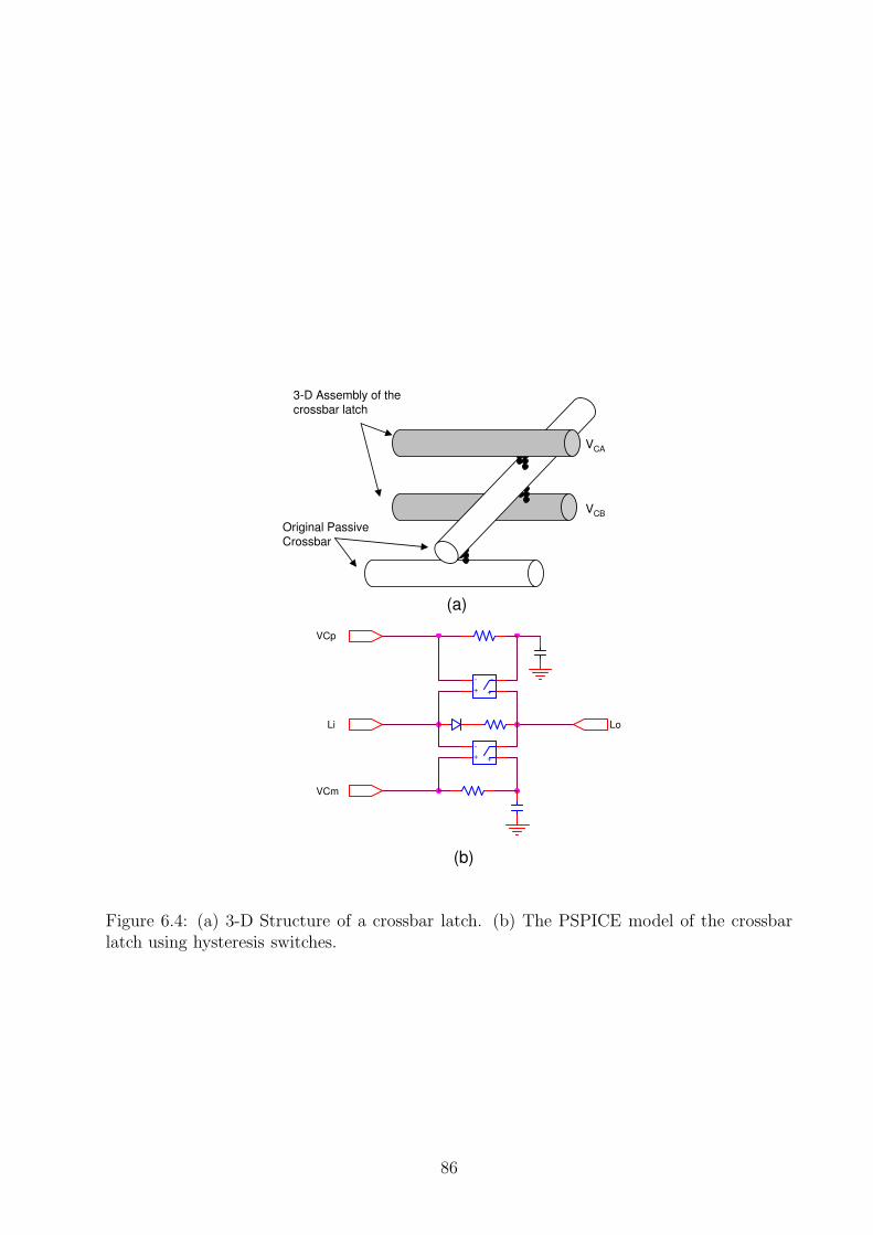
3-D Assembly of the crossbar latch
Original Passive Crossbar
VCA
VCB
+
-
+
-
+
-
+
-
LoLi
VCp
VCm
(a)
(b)
Figure 6.4: (a) 3-D Structure of a crossbar latch. (b) The PSPICE model of the crossbarlatch using hysteresis switches.
86

lines are shared among all the adjacent latches that are required to operate in the same
phase. Also microscale wires are expected to be the medium for a global signal in a wiring
hierarchy, and the control signals can be considered as global signals.
The current performance of these devices allows them to switch state for hundreds of cy-
cles, which is not enough for implementing continuously switching sequential logic. However,
these issues can be resolved by future advances in constructing the molecular compound used
as the switch.
6.4 Combinational circuit models
The regular structure of the crossbar array with passive devices resembles a PLA with AND
planes and OR planes. However, implementing the simplest sum of products functions
requires signal inversion. For example, consider a basic digital component as the full adder.
In the full adder, the carry out signal is given by C = xy + xz + yz which can be directly
mapped to the nano PLA. On the other hand, the sum signal S = x′y′z + x′yz′ + xy′z′ + xyz
requires inversion of all three input signals. The CMOL architecture provides a solution
to this by using microscale inverters and buffers [73]. This limits the integration density
advantage that can be achieved using nano scale electronics. The other approach that we
utilize here, is based on the crossbar model, discussed in the previous section. We use a
set of four control signals VCP1, VCM0, VCP0, VCM1. The control signals VCP1, VCM0 are used
for signal restoration while VCP0, VCM1 are used for signal inversion. The main difference
between the two pairs is the application of a voltage of opposite logic value to the original
signal value. The simulation model of a nanoscale crossbar full adder is shown in Figure 6.5.
This model is aimed at the integration of complete functionality at the nano scale. An
n-bit adder built using this model can be assumed to be pipelined if we utilize another set
of control voltages similar to the first set, but shifted in time. The shift is determined by
two factors; the circuit delay and the requirement to avoid control voltage induced spikes
87

A
B
C
clatch1
LoLiVCpVCm clatch2
LoLiVCpVCmclatch3
LoLiVCpVCm clatch4
LoLiVCpVCmclatch5
LoLiVCpVCm clatch6
LoLiVCpVCm
VCp1
VCm0
VCp0
VCm1
CarryCarry
Sum
Cout
S
Figure 6.5: A PSPICE model of a nano architecture model of a full adder, utilizing thecrossbar latches for signal restoration and inversion.
that feed through the switches. Phase-shifted control voltages allow every subsequent stage
to sample its input after it reaches a stable state. In this simulation, we chose that the
control signals sample the input to the circuit every 1µs, which is also the rate of change of
the least significant bit. Figure 6.6 shows another combinational example which is a 4-to-1
multiplexer built using the same idea.
This section demonstrates how it is feasible to implement any type of combinational logic
circuits using homogeneous nano-devices. In the next section, we will discuss the usage of
out-of-phase control signals for implementing sequential logic circuits. Out-of-phase control
signals are also used in combinational logic circuits in order to separate evaluation and
storage of different parts of the logic array. Part of the logic circuit evaluates its inputs,
when they are stored and stabilized in a prior stage. This is consistent with the concept of
pipelining. Isolation of each stage and its output is provided through the rectifying cross
connects. These cross connects are made of the same type of molecules but no control voltage
is applied to them.
88

Mux
S0
S1
A
clatch1
LoLiVCpVCm
clatch3
LoLiVCpVCm
clatch2
LoLiVCpVCm
clatch4
LoLiVCpVCm
B
C
VCp1
D
VCm0
VCp0
VCm1
Figure 6.6: 4-to-1 Multiplexer model using the crossbar latches in decoding the selectionsignal
6.5 Sequential circuits
The crossbar latch behaviour, described in Section 6.3 is analogous to a clocked D-type
latch with a single inverting or non-inverting output. This type of latch is suitable for
implementing shift registers and counters, which are necessary building blocks in a finite
state machine. The shift register effect requires isolation between the stages because in an
n-bit shift register, the next state of each bit is a function of the input bit.
In microscale circuits, this isolation is accomplished by the finite gate delay between the
input and output. In the crossbar circuits, the latches are taps on the signal line. Thus, a
shift register based on crossbar latches, represent a single signal line with multiple latches.
This would disrupt the shift register operation, because the signal will be essentially the
same at the end of the line as the input, when all the latches are unconditionally opened. To
overcome this, our design is based on a technique similar to the operation of charge coupled
89

devices (CCD). In one type of CCD operation, every other device is connected to the same
clock phase controlling the transfer. Also to force the signal to propagate in a single direction
and prevent shorting out the supplies, diode junctions are necessary to separate the stages.
Figures 6.7 and 6.8 illustrate a shift register and its simulation model. The arrows
between the latches on the signal lines represent isolation diodes, forcing signal propagation
in one direction without shorting supply rails, as would happen in a direct cascade of two
crossbar latches. Figure 6.9 shows the out-of-phase control signals used in clocking the shift
register and the simulation results of the crossbar-based shift register. The isolation diodes
are simply part of the wiring that interconnects two latches together and successive latches
can be arranged at 90o angles to each other.
Arbitrary sequence counters can be implemented by inserting combinational logic in
between the latches, in order to generate the appropriate input for the latches. The passive
combinational logic conducts the signals in one direction, and, thus it is not necessary to add
extra diode junctions. The structure of a generic counter and its crossbar implementation
are shown in Figure 6.10. In this architecture, the latching elements are parallel to each
other, and they all follow the same clocking sequence, as in the case of synchronous digital
logic. The layout, shown for the counter, can be improved in a straightforward manner,
using inspection or by using an automated tool that enforces a minimization of the layout
area.
Figure 6.9 shows the out-of-phase control signals used in clocking the shift register and the
flip-flop. The control signals are in excess of the assumed hysteresis voltage characteristics
of the proposed latch model. It also shows the simulation output of the shift register.
Another example is a circuit model for a T-flip-flop as shown in Figure 6.11. The proposed
model utilizes two-phase control signals and inversion control signals. The sum-of-products
is implemented using the diode array modeling a 2-to-1 multiplexer which selects either Q
or Q′ as the next state to be stored in the latch. The out-of-phase control signals are used to
90

D Q D Q D Qinput
clock
D Q
D Q D Q D Qinput
Ck1
D Q
Ck2
(a)
(b)
output
(c)
input
CK1
CK2
output
Figure 6.7: (a) A 4-bit shift register from D-latches. (b) Modifications to the basic shiftregister to make it suitable for crossbar implementation. (Two-phase control signals andrectifier junctions to force signal direction) (c) Crossbar implementation of the 4-bit shiftregister. (solid black arrows represent rectifier junctions, forcing signal direction)
separate between the ”evaluate” and ”store” steps. The ”store” is finished when the signal
is stable, and time-delayed from the feed through spikes at the transition of the hysteresis
switches. This architecture of the T-flip-flop can be cascaded, because it does not require
any extra inverters to produce the T and T ′ signals, used by the multiplexer portion. This
idea is shown in Figure 6.10c, in which intelligent mapping and reuse of resources results in
a very compact implementation of the counter.
6.6 Organization of a nano FPGA using crossbar arrays
The implementation of sequential circuits is necessary to implement configurable logic blocks
for nano FPGAs. FPGAs can be used to implement various nano-processors, as they are
91

VCp11
VCm01
clatch1
LoLi
VC
p
VC
m
Vx
VCp12
VCm02
clatch2
LoLi
VC
p
VC
m
clatch3
LoLi
VC
p
VC
m
clatch4
LoLi
VC
p
VC
m
R5
100k
Figure 6.8: A PSPICE model of the shift register using 2 pairs of out-of-phase control signals.
field programmable and have regular structures, which are the two main characteristics of
crossbar arrays. An FPGA slice can be composed of a lookup table, a latch and a wiring
matrix. The lookup table, the latch and the wiring matrix are all special forms of PLAs.
Thus the nano FPGA is an array of configurable logic tiles composed of patterns of these
simple structures. With the highly regular homogeneous organization of resources, the task of
organizing a nano PLA becomes greatly simplified. The same fabric is capable of performing
logic operations, and in addition to that, signal routing. A simple form of signal routing
is shown in Figure 6.12. Placement and routing have always been two distinct jobs, with
routing usually taking significantly more time than placement. In FPGAs, the tool may run
out of routing resources to implement the design even if the utilization of logic resources is
significantly less than 100%. This situation can be improved in a nano FPGA, since logic
resources can be exchanged with routing resources, and the placement can be dynamically
coupled with routing. This type of versatility, in conjunction with non-lithographic bottom-
up assembly, projects that nano electronics in the very near future will not only have superior
packing density to microelectronics, but will also require much less cost in terms of fabrication
and design time.
Since the whole structure is homogeneous, a place and route tool experiences great flex-
92
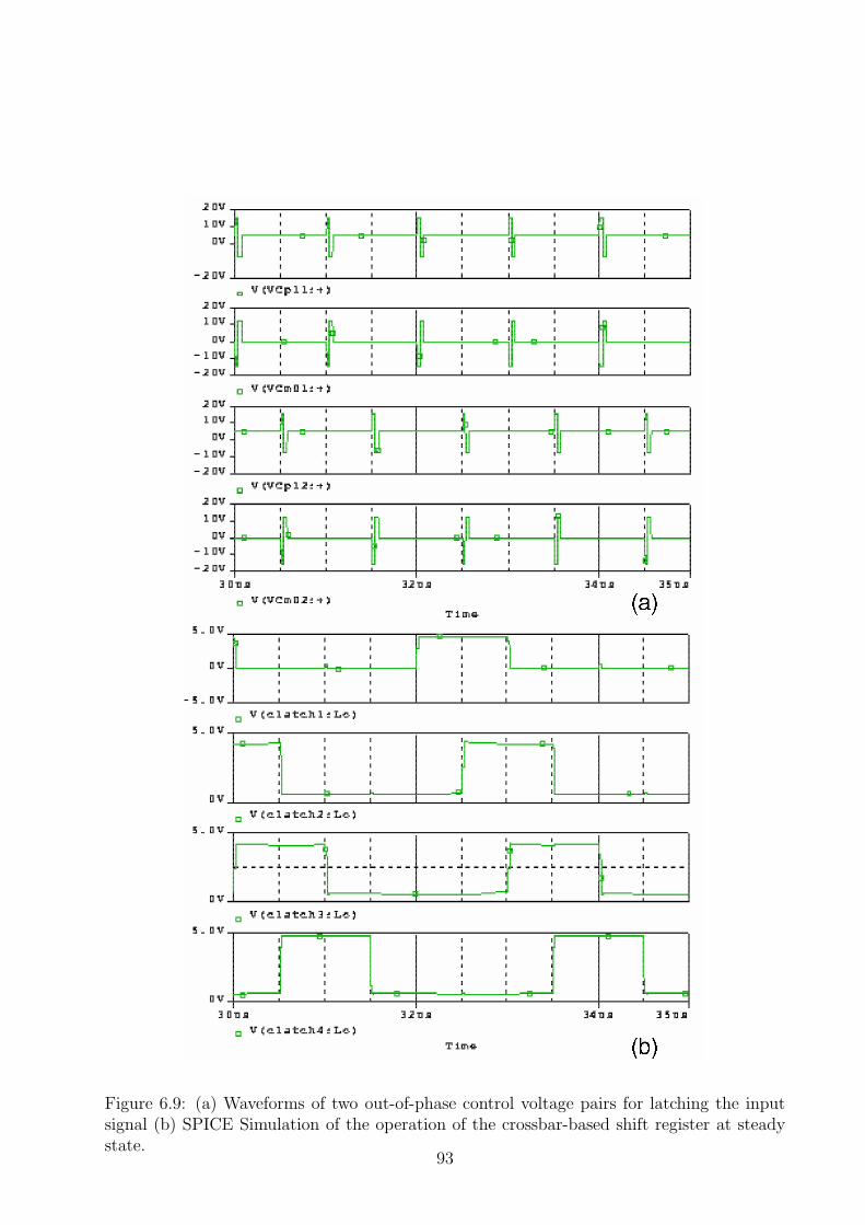
Figure 6.9: (a) Waveforms of two out-of-phase control voltage pairs for latching the inputsignal (b) SPICE Simulation of the operation of the crossbar-based shift register at steadystate.
93

D Q D Q D Qinput
clock
D Q
(a)
PLA PLA PLA
(b)
inputCK
AND
AND
OR
OR
Buffer/Invert
Latching Plane
AND
Plane
OR
Plane
AND
Plane
(c)
Figure 6.10: (a) A generic synchronous counter architecture with an arbitrary countingsequence. (b) Crossbar implementation of the generic counter requires only one controlsignal pair. (c) Floorplan of a generic counter.
Figure 6.11: A PSPICE model of a T-flipflop using a 2-to-1 MUX.
94

Figure 6.12: Shared routing/device plane
ibility in mapping a design. The only restriction that limits this flexibility is having to
periodically interface with the microscale circuits. This interfacing is required to provide
access to the input and output signals of the circuit, and to program each nanowire junc-
tion. The current solutions for addressing each junction are either using stochastic decoders,
or tilted arrays at an angle. This angle is a function of the nanowire pitch as compared
to the microscale wire pitch [33]. Figure 6.13 is an example of the organization of a nano
FPGA capable of both combinational and sequential logic. In this architecture, the building
component is a small PLA formed of AND/OR planes and buffering arrays. This building
component is placed on both sides of the vertical and horizontal axes, and is used to build
the pattern shown in Figure 6.13b. Larger PLA blocks can be incorporated to form macro
memory blocks. Thus, the architecture of a nano FPGA can be considered as inhomogeneous
from the macro level point of view (composed of different macro blocks), but it is homo-
geneous from a micro level point of view in which all the building blocks are side-by-side
crossbar arrays.
6.7 Area and timing of the nano FPGA
The area of a unit cell in a nano FPGA depends on the number of passive devices, number of
signal restoration devices and area overhead due to interfacing with lithographic scale wiring
95

AND
OR
Buffer
Connect
(a)
(b)
Figure 6.13: Example for the organization of the nano FPGA
96

and devices. In [35], the interfacing of nanowires with lithographic wires via stochastic de-
coders is how the nanoarray is programmed and this represents the major area overhead. The
second contributor to the area other than the logic itself is the stochastic buffering/inversion
devices within the array. In [35], the buffering/inversion is done by nanowire FETs. In [73],
the overhead due to interfacing with lithographic wires is overcome by tilting the nanoar-
ray relative to the lithographic array. This technique avoids using stochastic decoders and
guarantees the addressing of every cross point. However, in [73], signal restoration is carried
out by CMOS inverters and this greatly reduces the gain from using molecular devices for
the sake of higher packing density. In our circuit, we propose the use of the tilted array
technique in conjunction with cross bar latches. The 3D crossbar latch occupies one extra
cross point. In order to force signal isolation, a diode cross point is also necessary. Thus,
two extra cross points are required per buffer/inverter. The area of the nano crossbar for
building a nano FPGA slice can be approximately given by:
LUTnrows = 2×Ninputs + 1 (6.1)
LUTncols = 2Ninputs (6.2)
BuffInvcrosspoints = 2× LUTnrows + 4 (6.3)
NMUXSby1=(
S × 2 + 2S + 1)
× 2S + S × 4 (6.4)
SliceArea ≃ F 2nano(2× (LUTnrows × LUTncols
+BuffInvcrosspoints)
+2×MUX2by1 + 2×MUX4by1) (6.5)
where Fnano is the nanowire pitch. The areas of the multiplexers; MUX4by1 andMUX2by1, are
given by (6.4). One in LUTnrows stands for using one row in the OR plane, based on the as-
sumption that the PLA-based LUT has just one output. The number of input rows accounts
for every signal, and its complement as input to the PLA. The extra 4 BuffInvcrosspoints
97

account for assuming that a slice contains two latches. We also assume that a slice contains
four different multiplexers. Thus a four-input LUT can be considered as a PLA with 16× 9
cross points to account for the 16 possible minterms and the four inputs plus their inverted
counterparts and a ninth row for the OR function. If 8 crossbar latches are used at the LUT
input, and one at its output, then we need 18 extra crosspoints. This gives a total of 162
crosspoints per LUT plus latch. The typical FPGA slice contains two LUTs, some 2-input
multiplexers and 4-input multiplexers. Thus, the rough estimate of cross points per FPGA
slice is around 400. The area of a slice is, therefore, of the order of 40, 000nm2, assuming
that the nanowire pitch is 10nm. The overhead due to lithographic wires is at minimum,
based on the assumption that lithographic devices and nano devices are not in the same
plane. The typical area of CMOS logic at 22nm technology (state of the art at the time of
writing) is about two orders of magnitude higher.
The timing of the circuit depends on two main delay sources. The first delay is due to
the capacitance and resistance of the nanowires and cross points which affects the evaluation
time of the signal on the nanoarray. The second delay is associated with the time required
to program the molecular latch. Currently, the key delay component is due to programming
the molecular latch. The other component is not significant, since we do not use nanowires
for global signals. The approximate delay equations are given by:
Tclock = Tevalp + Topens + Tprograms + Tevaln (6.6)
Teval = Narray × (Ccrosspoint + Cwire)
×(Rcrosspoint +Rwire) (6.7)
where Tevalp is the evaluation time of the PLA prior to the crossbar latch, and Tevaln is the
delay time due to the resistance and capacitance of the interconnect, following the crossbar
latch till the next PLA block. If we assume the capacitance of a cross point to be 10−18Farad,
the contact resistances 1MΩ and neglect the resistance of the nanowire and its capacitance
to the substrate, then an array with 8 inputs will have a delay estimate of 10ps. The
98

Table 6.1: Comparison of nanoelectronic architectures
Architecture Nano PLA [35] CMOL [73] This work
CMOS to Stochastic Crossbar Tilt suggestedNanowire Decoders Tilt as [73]Restoration nanowire FET CMOS inverters Crossbar latchTiming Precharge RC delay RC delay
+ Evaluation + latchingArea Addressing CMOS inverter least
limited limited areaSequential FETs + Out of N/A Latches + Out ofCircuits phase Clocks phase clocks
programming time of the crossbar latch is still on the order of several milliseconds. As the
technology of fabricating molecular devices is advanced, this bottleneck will be removed.
Table 6.1 shows a comparative summary of the main features of our crossbar latch based
architecture and the architectures proposed in [35] and [73]. The mapping of finite state
machines using our circuit architecture is straightforward, and the mapped circuit can be
easily simulated using the models presented in the previous sections.
Since the full structure is homogeneous, a place and route tool experiences great flexibility
in mapping a design. The only restriction that limits this flexibility is having to periodically
interface with the microscale circuits. This interfacing is required to provide access to the
input and output signals of the circuit and to program each nanowire junction.
6.8 Fault and defect Tolerance in nano FPGA
The defect tolerance in FPGAs or in a nano FPGA follows the same ideas that are used
in manufacturing memories. Instead of throwing away the whole part, a scheme is used
to mark the bad blocks and avoid using them by a higher level software tool. In hard-
drives, a table is used for bad sectors to avoid using them. In memories, address remaping
is usually used such that the module externally appears as fault free with the addresses
99
remaped to redundant resources. FPGAs by definition are composed of redundant similar
blocks. The configuration tool can be used to map around the defects as in the Teramac
project [28,36,132]. The merit of such techniques in cross bar arrays is analyzed in [50]. Fault
tolerance is different because it has to deal with error during the operation such as failure
of one block or faults due to transient errors and noise [118]. The Dual-FPGA architecture
developed in the ROAR (Reliability Obtained by Adaptive Reconfiguration) project at the
Stanford Center for Reliable Computing is an example of the design of reconfigurable system
with the capability of ”on-line” error detection, recovery and self-repair. The techniques
for fault detection use error masking techniques, triple modular redundancy and software
reconfiguration [82]. These techniques follow what we discuss in chapter 3 and can be adapted
easily to the nano-scale because they are all high level and are not directly associated with
the technology itself.
One example for error detection and autonomous repair can be built using a dual self-
checking pair (DSCP) system shown in Figure 3.1. This figure is repeated here as Figure 6.14
for convenience. In this system, each one of the four blocks, forming the two pairs, is a
reconfigurable array. Initially, a defect scanning system maps all the defects in the four
blocks. A configuration system then configures all four blocks to do the same functionality.
The second pair (”B” pair) is placed in standby. Calculations are performed in parallel by
the first pair. When a discrepancy occurs between their outputs, the high level configuration
system switches the calculations to the second pair. The defect scanning system analyzes,
the first pair to find a new map of defects and then reconfigures them using the redundant
available resources in each block. This is the repair step. Once the pair of blocks is repaired,
they are placed in standby until an error is detected in the active pair, and then the process
is repeated. This can repeat any number of times as long as there are available unused
resources in each one of the blocks.
100

Figure 6.14: Dynamic fault tolerant system
6.9 Conclusion
The regular structure of the crossbar array has been utilized in the literature to implement
simple PLA-like structures. However, these structures are not capable of integrating ho-
mogenous devices for signal buffering, restoration and inversion. In this chapter, we utilize
the crossbar latch to present the implementation of a complete nano scale system that is
independent from the microscale electronics except for initial programming and signal I/O.
The proposed circuit model was used in simulations of simple combinational and sequential
circuits in order to verify the concept of operation. Utilizing this full adder in an accumula-
tor is straightforward since the proposed circuit model is inherently pipelined and supports
signal latching. The crossbar latch is a homogeneous device within the crossbar array used
to implement the passive combinational circuits described so far in the literature. The se-
quential circuits proposed, are based on the crossbar latch and, thus, are more feasible to
implement compared to the previously described non-homogeneous structures. Such logic
structures are necessary for implementing finite state machines which are major building
blocks in a true nano FPGA and nano processor systems. As a proof-of-concept, we showed
successful simulation results for a simple shifter and structure and simulation of a T-flipflop.
We illustrated a possible organization of a nano FPGA, capable of performing both sequen-
tial and combinational logic and is composed of regular repetition of one type of device
101

resources. The architecture of a nano FPGA or a nano processor can be inhomogeneous
from a macro level point of view in the sense that it is composed of finite state machines,
memories, shift registers, adders,. . . , etc. However, all the blocks of a nano processor are
composed of the same building fabric; (the crossbar array), and, thus, can be implemented
using the simple bottom-up assembly fabrication techniques. An automation tool can di-
rectly map complex macro level functionality onto the crossbar fabric and convert parts of
it into crossbar latches. The latches or buffering arrays can be either inserted at the points
where the signal levels are degraded due to passing through a sequence of passive devices, or
simply inserted periodically. Defect tolerance is carried out by defect mapping and routing
around defects. Fault tolerance requires dynamic reconfiguration, and it can be implemented
at a higher level of design hierarchy, which monitors the performance of the circuit.
102

Chapter 7
Quantum Computing Alternative
In the previous chapters, we studied classical circuits that rely on quantum effects for their
operation such as the WPG device used in the hexagonal array and the hysteresis switch
used in the crossbar array. In this chapter, we look at using the quantum effects directly in
the form of quantum computation. We then investigate the possibility of implementing a
conventional computing architecture that can practically emulate the functionality of a hy-
pothetical quantum computer. Quantum computing algorithms are superior to conventional
algorithms because they can be used to evaluate multiple possibilities for the input values
in parallel using one set of hardware resources.
7.1 Introduction
The origin of quantum mechanics roots in describing physical phenomena that can not be
described by classical Newtonian physics. In quantum mechanics, energy is quantized, i.e.
takes discrete values. The black body radiation catastrophe is the failure of classical mechan-
ics to predict the radiation energy from a black body at increasingly shorter wavelengths.
The classical prediction was that the energy would indefinitely increase. Infinite energy ra-
diation is impossible and nonsensical. Max Planck’s proposal that the energy is quantized
produced a theory that perfectly matches the measured phenomenon and solves the prob-
lem. Einstein described light to consist of particles (photons), instead of just a classical
electromagnetic wave, in order to correctly explain the photo-electric effect. Electrons are
particles that exhibit wave like interferences as they pass through a double slit apparatus.
De Broglie, later, proposed that every particle is associated with a wave. The Schrodinger
wave equation describes the evolution of the wave associated with the particle and can be
103

used to calculate the energy of the particle and its position.
Matrix mechanics is an alternative way of describing the same physical phenomena by
using matrix algebra instead of solving Schrodinger’s equation. With time, quantum me-
chanics and matrix mechanics became one and the same. Due to certain properties of
matrix algebra, new properties of the physical systems have to be inferred. For example, the
Heisenberg uncertainty principle is a consequence of the non commutative property of ma-
trix multiplication: AB −BA 6= 0. Observables are physical properties of the system (like
position, momentum, energy, ...etc.). In matrix (quantum) mechanics, they are described by
Hermitian 1 operators in Hilbert space 2. Since matrix multiplication is non-commutative,
a measurement of position followed by a measurement of momentum is not equivalent to
measurement of momentum first then measurement of position. This leads to uncertainty
or error and thus, the Heisenberg’s uncertainty principle.
According to matrix (quantum) mechanics, a measurement on a system would give one
of the eigenvalues of the system, where the system state is described as a superposition of
eigenvectors with different complex weights. The Max Born rule states that the probability
of measuring such an eigenvalue is equal to the amplitude squared of such complex weights.
Quantum mechanics is now described as quantum physics. Quantum physics is now the
general theory to describe the world and classical physics is considered an approximation of
quantum physics when particles and their energies are described by quantities much larger
than Planck’s constant. The classical approximation in this case will be adequate because
the difference between energy quantum levels will not be measurable and continuum of
energy becomes a valid assumption for this class of particles. Also the wave properties
become impossible to observe as the particle size becomes much larger than its associated
wavelength which is given by De Broglie’s equation λ = hp.
1A Hermitian is a self adjoint matrix in which the matrix is equal to the complex conjugate transpose ofitself. U = U
†
2Hilbert space is a vector space with a norm (means length of a vector in that space is defined).
104

7.1.1 The qubit
Quantum computers are computers that utilize quantum bits arranged in a quantum register
as opposed to classical computers which use regular bits. In physical reality, a qubit is a
physical subsystem that can be described by two states. For example, a photon is a physical
system which we can described in terms of multiple physical subsystems. One possible
subsystem is the photon polarization which can take two states; either horizontal or vertical.
Another physical subsystem of the photon is its direction of travel inside a MachZehnder
interferometer (or even the Michelson interferometer) which restricts the direction of travel
to one of two possible value. Another physical system is the electron. A two state subsystem
of the electron is its spin which can be either up or down as in the Stern-Gerlach apparatus.
There are two main similarities between a classical bit and a quantum bit (qubit). The
two similarities are that the initial state of a qubit is always set to either zero or one and
also the final measured state of a qubit is either zero or one just as a classical bit. A
qubit, however, during computation is a superposition of the states one and zero and the
amplitudes of the superposition components are indication of the probabilities of measuring
the outcome of the computation at a certain level in the quantum circuit. A quibit in either
one state or a superposition of a state is described as being in a pure state. The mixed state
describes an ensemble of particles that follow a statistical distribution and the constituents
of that ensemble can take multiple values as in unpolarized light composed of an ensemble
of photos.. The mixed state is not the superposition state which describes the state of one
particle alone.
The qubit using Dirac’s notation is usually written as
|ψ〉 = α0 |0〉+ α1 |1〉 (7.1)
where the ket operators are vectors representing the two states of the system. These two
states are usually denoted as the state −1 (or spin down) represented by |1〉 and the state
105

Figure 7.1: Possible physical realizations of a qubit as a physical subsystem of a certainphenomenon. (a)The photon direction of travel is restricted to one of two values as inthe Mach-Zehnder interferometer with one photon entering the apparatus. (b)Single photondirection of travel in the Michelson interferometer with the directions not necessarily perpen-dicular but the system states are nevertheless orthogonal. (c)The Stern-Gerlach apparatuswith the electron spin (up or down) as the qubit.
106

+1 (or spin up) is represented by |0〉.3 |0〉 is
1
0
and |1〉 is
0
1
The rule that governs the coefficients α0 and α1 is that the sum of their squares must be
equal to one since the squares give the probabilities of measuring each state according to
the Max Born rule. Thus, apart from the initial set state and the final measured state,
the in-between computation internal state (or hidden state) of a qubit must be stored by
a classical computer in two complex fixed point registers because in general the coefficients
are complex and the qubit representation is on the surface of a Bloch sphere.
The maximum value of either coefficient is just one and thus we may assume that a
floating point representation is not necessary. If we assume that a 10-bit fixed point number
representation is sufficient precision for the coefficients then this translates to 40 bits of
classical storage just to represent the internal state of one qubit. However, since we still
have the constraint that the sum of the squares of the amplitudes must equal one then we
need to store only 3 real numbers. The internal qubit state may also be represented as a
density matrix given by
ρ = 0.5(I + βxσx + βyσy + βzσz) (7.2)
where βx, βy, βz are real numbers and I, σx, σy, σz are the Pauli matrices. The elements
of the density matrix directly represent the probabilities of the measurements performed on
the system. The Pauli matrices represent rotations around the Cartesian axes and they are
3It may be confusing to say that 1 is represented by a 0 but this is not the only context in which suchnotation is used.
107

Figure 7.2: Bloch sphere representation of possible states of a single qubit
given by:
σ0 = I =
(
1 00 1
)
(7.3a)
σx = X =
(
0 11 0
)
(7.3b)
σy = Y =
(
0 −ii 0
)
(7.3c)
σz = Z =
(
1 00 −1
)
(7.3d)
Since β2 = βx2 + βy
2 + βz2 = 1 on the surface of a sphere of radius 1, the spherical
coordinates r, θ, φ can be used with r = 1. Thus, actually only two parameters may be
needed to represent a qubit. The general representation for a qubit is
α0 = eiγcos(θ/2) (7.4)
α1 = eiγeiφsin(θ/2) (7.5)
γ is an overall phase factor that can be ignored because it is not observable [61, 77]. We
only need θ and φ. This means that two complex numbers which are actually four values are
represented in this case by only two values. One value is omitted because of the constraint
and the other is omitted because it is not observable. The Bloch sphere representation is
shown in Figure 7.2.
108
7.1.2 A system of more than one qubit
There is not much computation that can be done using one qubit. Since the initial state of
a qubit is set as 0 or 1 and the final measured state is also either 0 or 1, it is possible to say
that a single qubit computer cannot be more useful than a single bit computer that can only
do four elementary operations. These operations are: store 0, store 1, invert and leave as is.
If we consider the case of having two qubits, we begin to realize that there is a big difference
between two qubits and the case of two classical bits. if the state of the first qubit is Q1 and
the second qubit is Q2 then the state of the system of the two qubits is given by the tensor
product Q2 ⊗Q1. For example if Q1 = |0〉 and Q2 = |1〉 then the system state is 4
(
01
)
⊗(
10
)
=
0010
The alternative ways of writing this state are |1〉 ⊗ |0〉 or |1〉 |0〉 or |10〉
The state of two qubits is in general a superposition of the states |00〉, |01〉, |10〉, |11〉.
Where |00〉 is given as the vector
1000
and |01〉 =
0100
... etc.
ψ = α00 |00〉+ α01 |01〉+ α10 |10〉+ α11 |11〉 (7.6)
The initial interpretation of equation 7.6 in terms of hardware comparison between a
classical computer with two bits and a quantum computer with two qubits is that while
the two bits have a space of 4 values in which they can take only one value at a time,
the quantum bits are actually represented in a Hilbert space where they take all possible 4
values simultaneously at any step of the computation. The only restriction is that the sum of
the squares of the probability coefficients is 1. Thus, the internal (hidden) value of two bits
occupies just 2 bit locations. However, the hidden value of two qubits requires representation
by 4 complex fixed point registers (or 7 floating point numbers due to the constraint). In
general the hidden state of a quantum register with n qubits requires 2 ∗ 2n − 1 classical
4In Matlab: kron([0;1],[1;0])
109

fixed point registers. To illustrate this further consider that we need 128 qubits to solve a
certain problem. While a 128 classical bits can take any value in 2128 space, they can only
take one of these values at a time and to know the state of 128 bits we need to read exactly
128 bits. The state of a quantum register, however, may take the 2128 states simultaneously
and to store that in a classical computer we need to store the hidden value in a memory
with 128 address bits. This is a very large memory address space by today’s standards.
It is also required to update all the memory space at every step in the computation due
to entanglement. This example illustrates why the quantum computer is inherently more
powerful than a classical computer and why it would take a classical computer exponential
time and exponential resource requirements to emulate a quantum computer. The trivial
case, in which a qubit is stored in a single memory location capable of holding two complex
values and our 128 qubit example would translate to requiring only 128 memory locations
instead of 2128, is only valid if all the qubits are isolated from each other and not considered
in a single closed system [55].
7.1.3 Entanglement
Entanglement is a state of the quantum system in which, one operation on one qubit will
instantaneously affect the outcome of other qubits. This happens regardless of the distance
separating the two qubits and in an instantaneous sense that if we were to assume commu-
nication taking place between the two qubits, the information transfer has to happen at a
speed greater than the speed of light [41]. One interesting interpretation of entanglement
from reference [77] is that Bob and Alice got married and thus their lives became entangled.
After Alice became pregnant, Bob left on a trip at a speed close to the speed of light to the
edge of the galaxy. When Alice gave birth, Bob’s state instantaneously changed into a father
without any delay in communication or even requirement of communication. Assuming that
the state change required communication to take place then the special relativity theory is
violated.
110

In the Bell state, two qubits are called an EPR pair after Einstein, Podolsky and Rosen
who considered this interesting behaviour. In this state, a measurement of the first qubit
may yield either a zero or a one with equal probabilities. A subsequent measurement of the
second qubit, however, will yield the exact same outcome as the measurement of the first
qubit. The state of a system can be calculated by the tensor product of individual qubit
states. Inversely, we can factorize a state vector into a tensor product in order to arrive at
the contribution of each particle in the system. However, it is not always possible to make
this factorization. For example, the Bell state given by α00 = α11 = 1/√2 and α10 = α01 = 0.
or
ψ =1√2(|0〉 |0〉+ |1〉 |1〉) (7.7)
cannot be factorized into a tensor product. This means that the system state cannot be
described in terms of the contributions of its individual constituents. Another way to look
at it is the following: If the starting state of the system is
ψ = α00 |00〉+ α01 |01〉+ α10 |10〉+ α11 |11〉
and we make a measurement on the rightmost qubit alone and find out it is a zero, then the
system we are left with is described as ψ′q0 = α′
00 |00〉+ α′10 |10〉.
If the measurement yields a one in the rightmost qubit then the system state becomes
ψ′q0 = α′
01 |01〉+ α′11 |11〉.
If from the start, the states |10〉 and |01〉 did not exist, then measuring a zero in the rightmost
qubit will lead to a definite measurement of zero for the leftmost qubit and measuring a one
111

leads to a definite measurement of a one. The four Bell states for two qubits are:
ψ00 =1√2(|0〉 |0〉+ |1〉 |1〉) (7.8a)
ψ01 =1√2(|0〉 |0〉 − |1〉 |1〉) (7.8b)
ψ10 =1√2(|0〉 |1〉+ |1〉 |0〉) (7.8c)
ψ11 =1√2(|0〉 |1〉 − |1〉 |0〉) (7.8d)
The four Bell states for two qubits are linked by unitary transformations. Unitary transfor-
mations do not change the entanglement because they are reversible [104].
Multi-particle entanglement is defined using the GHZ state5 and the W state where for
N particles [46].
|GHZ〉 = 1√2
(
|0〉⊗N + |1〉⊗N)
(7.9)
|W 〉 = 1√N
(|1000〉+ |0100〉++ |0001〉) (7.10)
7.1.4 Quantum gates
The gates are a mathematical abstraction of the possible mathematical operations that can
be carried out on one or more qubits. In digital logic, all logic operations can be defined in
terms of a universal gate which is the Nand gate. In quantum computation, it is also possible
to define a set of universal gates that can be used to describe the computational steps of any
algorithm. One such set of gates is composed of single qubit operations (rotations) and two
qubit operations (controlled-Not or the quantum XOR).
5Greenberger - Horne - Zeilinger state
112

|φ〉 = H |ψ〉 = 1√2
1 1
1 −1
α0
α1
=1√2
α0 + α1
α0 − α1
=α0√2(|0〉+ |1〉) + α1√
2(|0〉 − |1〉) (7.11)
Other single qubit gates are the S, T , phase shift P , R, rotation operators R§,R†,R‡
and their complex conjugates.
S =
(
1 00 i
)
(7.12)
T =
(
1 0
0 eiπ4
)
(7.13)
Pθ =
(
eiθ 00 eiθ
)
(7.14)
Rθ =
(
1 00 eiθ
)
(7.15)
Rx(θ) =
(
cos(θ/2) −i sin(θ/2)−i sin(θ/2) cos(θ/2)
)
(7.16)
Ry(θ) =
(
cos(θ/2) − sin(θ/2)sin(θ/2) cos(θ/2)
)
(7.17)
Rz(θ) =
(
e−iθ/2 00 eiθ/2
)
(7.18)
Two qubit quantum gates are in general called a controlled-U operation, where U is
a rotation operation carried on one qubit. The other qubit is used as the control of the
operation such that the rotation operation is carried out if the control qubit is equal to
|1〉 and the target qubit is left as is if the control qubit is |0〉. As an example, the CNOT
gate (controlled NOT) which has the classical equivalent, the XOR gate. The input to the
CNOT is a two qubit system whose state is given by |ψφ〉. This state can be found using
a tensor product and thus |ψφ〉 =
(
α0β0 α0β1 α1β0 α1β1
)T
. The operation of the
113

Figure 7.3: CNOT gate
CNOT (XOR) is represented by the matrix
GCNOT =
1 0 0 00 1 0 00 0 0 10 0 1 0
(7.19)
The symbol for the CNOT is shown in Figure 7.3.
Gates that operate on three qubits are the Fredkin and Toffoli gates. The Toffoli gate is
a controlled-controlled-Not gate or CCNOT. It flips the third bit if both the first two bits
are 1. The Fredkin gate is a controlled-swap gate. It swaps bits two and three if the first bit
is 1.
GToffoli =
1 0 0 0 0 0 0 00 1 0 0 0 0 0 00 0 1 0 0 0 0 00 0 0 1 0 0 0 00 0 0 0 1 0 0 00 0 0 0 0 1 0 00 0 0 0 0 0 0 10 0 0 0 0 0 1 0
(7.20)
GFredkin =
1 0 0 0 0 0 0 00 1 0 0 0 0 0 00 0 1 0 0 0 0 00 0 0 0 0 1 0 00 0 0 0 1 0 0 00 0 0 1 0 0 0 00 0 0 0 0 0 1 00 0 0 0 0 0 0 1
(7.21)
7.1.5 Matrix expansion and refactoring for quantum gates
The elementary gate operations are usually defined in terms of the exact number of qubits
that they operate on. Single qubit gates are described using 2 by 2 matrices. A two qubit
114

gate such as the CNOT has a 4 by 4 matrix which represents an operation on two qubits
where the leftmost (MSB) is the control qubit and the LSB qubit is the target. Fredkin and
Toffoli gates are described using 8 by 8 matrices with the target being the LSB qubit. Since
the size of a quantum register is arbitrary, say 8 qubits, and a CNOT gate may be used
with qubit 5 as the control and qubit 3 as the target for example, then how can the unitary
28by28 operation matrix be generated from the 4by4 CNOT matrix in equation 7.19? For
single qubit operations such as the Hadamard gate for instance, it is easy to generate the
required unitary matrix. For example, if we want to apply the Hadamard gate to the 6th
qubit in an 8 bit quantum register described as |Q7Q6Q5Q4Q3Q2Q1Q0〉 then the operation
is given by I ⊗H ⊗ I ⊗ I ⊗ I ⊗ I ⊗ I ⊗ I, where I is the 2by2 identity matrix.
The general algorithm to generate the operation matrix, from any arbitrary one/two/three
qubit gates, is the following [127]:
1. Let matrix M (2n × 2n) be the desired operation matrix from the gate matrix
G (2m × 2m) where m < n
2. Let Q be a set of the indices of the qubits in the n qubit register that G should
operate on. Q’ is the set of the remaining indices.
3. Let Mij = 0 if the binary representation of i differs from the binary represen-
tation of j at the bit positions identified by the numbers in the set Q’.
4. Otherwise, let Mij = Gi∗j∗ where i* is the number constructed by concatenat-
ing the binary bits of i at the bit positions identified by the numbers in the
set Q. Same for j*.
It should be noted that we can avoid memory issues and not store matrix M at all. Every
generated element of M row-wise can be multiplied by the system state and the accumulated
result gives the corresponding row element in the new system state vector.
115

7.1.6 Quantum algorithms and the realization of quantum computers
In [123], Peter Shor classifies the known quantum algorithms into three categories. The first
category is based on using the Fourier transform to find periodicity. Under this category is
the factoring and discrete logarithm algorithms [122]. The second category contains Grovers
search algorithm, which can perform an exhaustive search of N items in time of the order√N [47]. The third category consists of algorithms for simulating or solving problems in
quantum physics as proposed by Feynman in 1982.
The basic implementation of a real quantum computer relies on trapping a particle that
exhibits quantum behaviour and manipulating this particle or group of particles using an
external stimulus. The last step is to read the result of the manipulation (calculation)
before the decoherence time has elapsed. Decoherence time limits the number of faultless
gate operations that a quantum circuit can perform.
Some of the known prototype implementations of quantum computers use techniques
such as the ion trap method, linear optical manipulation, the magnetic resonance technique
and super conductivity.
In summary, the steps needed in a quantum computer [150]:
• Initialize qubits to a known state.
• Implement one-qubit gate operations.
• Implement two-qubit gate operations.
• Measure the state.
• Isolate the system from the environment during the gate operations and the
measurement.
116

Optical quantum computers
These computers are based on manipulating photons generated from a laser source using
optical devices such as mirrors, beam splitters and optical filters [64,111]. Single-qubit gate
operations are performed using mirrors, beam splitters and phase shifters. Measurement
is done by single photon detectors. Photons tend not to interact with each other and thus
two-qubit gates are very difficult to implement and requires many devices and extra photons.
Entangled photons can be produced from a single source using a process called parametric
down conversion [154].
One way quantum Computers
A One-way quantum computer or cluster state quantum computer (QCC) is a model of a
universal quantum computer [22,110,146]. One possible implementation is based on photons.
The one-way quantum computer does not perform quantum logic on the individual qubits of
the cluster state. In this structure, a highly entangled state, called the cluster state, allows
for quantum computation by single-qubit measurements only. Because of the central role of
measurement, the one-way quantum computer is irreversible because measurement destroys
the state. The computation is performed in the following way:
• Qubits of QCC are brought into cluster state, which is independent of algo-
rithm and input, i.e. independent of the computational problem.
• Information is put in, processed and read out by single-qubit projective mea-
surements in directions depending on algorithm, input and sometimes on pre-
vious measurement results.
In the QCC , entangling the whole cluster once and subsequently performing all the mea-
surements is equivalent to simulating a quantum logic network gate by gate. The order and
choices of measurements determine the algorithm computed.
117

NMR based quantum computers
In NMR quantum computers, molecules in a fluid are manipulated by a magnetic field in a
fashion similar to magnetic resonance imaging. Operations are performed on the ensemble
of molecules through magnetic pulses applied perpendicular to a strong, static field, created
by a large magnet.
Ion traps based quantum computers
In ion traps, an atom is converted into an ion. The ion is confined in a trap by means of
an electromagnetic field acting on the charge. A laser is used to perform four tasks based
on the location where it hits, its energy and pulse width. The first task is setting the value
of the qubit by pumping the atom into a higher energy state. The second task is to apply
one-qubit operations and the third is applying two quantum gate operations. The fourth
task is measuring the state of the ion. Entanglement is the case of ions being strung together
in the field by their common vibrational modes. The main drawback of this technique is its
lack of scalability and slow operation.
The RezQu architecture
The RezQu architecture is a recent development. The Resonator/zeroQubit (RezQu) archi-
tecture is one of the enhancements to quantum states built out of superconducting circuits
using Josephson junctions.
7.2 Simulation of quantum computers
By simulation of a quantum computer we mean the implementation of the circuit model of
quantum computation, that was introduced by Deutsch, on a classical computer. The circuit
model is the model that describes the step by step evolution of the state of the quantum
register due to the application of reversible gates. Most of the simulation techniques involve
implementing matrix multiplications in one way or another. The operations involve applying
118

a 2n × 2n matrices representing a unitary operator to a 2n register holding all possible
superposition states of an n qubit system [107, 120]. Reduction of the complexity of matrix
multiplication resource requirement is the main issue in most of the literature as pointed out
in reference [56]. Quantum Information Decision Diagrams (QuIDD) is a technique that uses
Algebraic decision diagrams (ADD) in order to reduce the memory requirements for storing
the matrices [143, 144]. In this technique, the fact that the unitary operators involved in
circuit simulations are greatly regular and greatly sparse, is used to build decision diagrams
that represent the matrix. The benefits of such approach diminish quickly with increased
entanglement. Quantum multi-valued decision diagrams (QMDD) is another approach for
storing the matrices using decision diagrams to achieve similar goals with the benefits of less
memory requirements and faster simulations than QuIDD. These benefits can be attributed
to the difference in the implementation of the decision diagram simulator in QuIDD and
QMDD [43,80]. Worst case scenario still requires exponential complexity. The reason behind
this dead end is the mathematics involved in describing quantum systems. It is not possible
to describe a system in terms simpler than a mathematical formulation and in this case the
mathematical formulation requires exponential resources. The only way around this is to
invent new mathematics or a new mathematical formulation. The existing matrix and tensor
based formulation does not map to physical space. In the case of 2 qubits, the space is at
least 6 dimensional and has no intuitive interpretation.
7.3 Emulating quantum computation using classical resources
The direct method to emulate quantum computation is to build a system that computes
matrix operations and stores the intermediate results in registers. This is shown in Figure 7.4.
These intermediate results represent the hidden state of the quantum register. Measurement
can be emulated using pseudo-random number generators. This requires value thresholds
that are calculated in accordance with the squares of the amplitudes of the complex numbers
119

Figure 7.4: Direct implementation of a quantum emulator using registers and matrix oper-ations represented by gates
as stated by the Max Born rule. There are many attempts to implement this direct approach
in the literature [45, 62, 140]. This direct approach suffers from the problem of exponential
resource requirements, and it is limited to very simple operations. In the next sections, we
investigate the requirements of a quantum computer emulator and whether it is possible to
fully implement it using classical resources.
7.3.1 Approximate storage requirement for emulating a qubit
The storage requirement of the values of θ and φ from equation 7.5 depend on the practical
choice of angle resolution. The angle resolution can be a fixed parameter or a dynamic
parameter as we will show in the practical quantum emulator. The representation of the
angle projections of a point on the sphere requires lookup tables for the sin and cos functions.
The lookup tables are indispensable since the operations on more than one qubit will involve
the manipulation of α0 and α1 (or sin(θ/2), sin(φ), cos(θ/2) and cos(φ) ) not the angles
themselves unless the operation is a pure rotation carried on one qubit only. In fact all
the elementary operations that can be performed on a single qubit are only rotations. The
number of entries in the lookup table is a function of the angle resolution while the number
of bits per entry is a function of the required precision of the representation of the sin and
cos functions. It is sufficient to store sin / cos pairs of 1/8 of the angles between 0 and 360
120

Table 7.1: Sin/Cos reduced lookup table by exploiting Sin/Cos octant symmetry
Angle sin cos0 : 45 sin(0 : 45) cos(0 : 45)45 : 90 cos(45 : 0) sin(45 : 0)90 : 135 cos(0 : 45) − sin(0 : 45)135 : 180 sin(45 : 0) − cos(45 : 0)180 : 360 − sin(0 : 180) − cos(0 : 180)
or just up to the 450 angle. This can be explained by that the values of the sin function
for the angles from 45 to 90 are identical to the values of the cos function for the angles
decrementing from 45 to 0 while the cos of the angles from 45 to 90 are identical to the
values of the sin function for the angles decrementing from 45 to 0. Thus for the angles 45
to 90 we only need to reverse the reading of the lookup table and swap the values of the sin
and cos. By symmetry we get the values of the sin and cos in the other 3 quadrants by just
manipulating a sign bit as shown in table 7.1.
7.3.2 Qubit representation using algebraic integers
Storing tables of trigonometric function values using finite precision leads to accumulating
errors in the emulation of quantum calculations. To avoid this problem, algebraic integers
can be used to represent a complex number [75]. A complex number can be represented by
the following equation:
Z(ω) =
R/2−1∑
j=0
ajωj (7.22)
where ajǫZ (set of integers), and ω = e2πR . When R = 4, this represents the usual way of
representing a complex number using a real part and an imaginary part, albeit the numbers
used are restricted to being integers. These integer values are an interpretation of the
finite number of bits used to represent a number in memory. When R = 12, which means
six integers are used to represent a single complex number, the representation becomes
dense and greater accuracy can be achieved in the computation as shown in Figure 7.5.
121

Mathematical operations such as addition and multiplication are defined on the algebraic
integer representation [76].
7.3.3 Emulating superposition of states
Systems that deal with multiple logic values in excess of two, usually use multiple wires
to represent a single value. Digital communication systems deal with binary signals, but
may transmit several data streams simultaneously in a single channel (space as the typical
single communication channel). These (transmit/receive) systems are digital computers
that represent information in an analog form and superimposes multiples of data sources in
a single channel. We can exploit this analogy to build a system that has multiple states in
a single wire and thus greatly reduce the number of circuit elements required to handle the
information. This system would store the internal (hidden) state of the quantum system
using a system of orthogonal signal generators. These signal generators can be random noise
generators, or sinusoidal generators, or even generators of dilated wavelet bases. A single
hardware FFT-calculator block; from an OFDM system, can be used to generate all the
sinusoids required to emulate the state of a quantum register in superposition.
Wavelets can produce similar results with better spectral performance than time gated
sinusoids, because of their inherent fast spectral decay. Orthogonality is inherent in con-
structed wavelets such as the Daubechies family of wavelets, because it is a condition in
their construction. Dilated/translated versions of a Haar wavelet are clearly orthogonal as
shown in Figure 7.6. A similar diagram for a Daubechies-2 wavelet has a similar characteristic
although it may not be clear from the plots in Figure 7.7.
7.3.4 Emulating entanglement
Although entanglement is different from classical correlation in the sense that it does not re-
quire physical communication or interaction between the entities, we may still try to emulate
it using classical methods. The method we investigated is to have control signals between
122

−2 −1.5 −1 −0.5 0 0.5 1 1.5 2−2
−1.5
−1
−0.5
0
0.5
1
1.5
2R=4 variables=2
Real part
Imag
inar
y pa
rt
(a)
−8 −6 −4 −2 0 2 4 6 8−8
−6
−4
−2
0
2
4
6
8R=12 variables=6
Real part
Imag
inar
y pa
rt
(b)
Figure 7.5: Complex number representation using algebraic integers (a)R=4 or using 2variables. (b)R=12 or using 6 variables.
123

0 0.5 1 1.5 2 2.5 3 3.5 4 4.5−1
0
1
0 0.5 1 1.5 2 2.5 3 3.5 4 4.5−1
0
1
0 0.5 1 1.5 2 2.5 3 3.5 4 4.5−2
0
2
Figure 7.6: Orthogonality of dilated Haar wavelets. The translation is zero.
0 2 4 6 8 10 12 14−1
0
1
2
0 2 4 6 8 10 12 14−1
0
1
0 2 4 6 8 10 12 14−2
0
2
Figure 7.7: Dilated Daubechies-2 wavelet.
124

the qubit signal generators. If a qubit is represented as a phase locked loop (PLL) with
its control voltage coming from another PLL, then by manipulating one PLL (one qubit),
we immediately change the output (state) of the other. We tried to extend this idea to
more than two qubits with no success because it does not scale. The number of connections
required will still be exponential and the system will take time to reach a stable state. The
model for such connectivity and control is the vector representing the state of the quantum
register. This vector is a simple representation, and it is not possible to use a more complex
representation (such as PLLS and control voltages) in order to reach a simpler representation
than the starting point. In fact, a mathematical representation is the simplest representa-
tion, and is a terminal end. It is used to model a physical system. However, a physical
system can not be used to efficiently model a mathematical representation. Although this
result may seem obvious, the large number of attempts to build a quantum emulator proves
otherwise. The reason in my opinion, is that the mathematics used in quantum mechanics
seems very simple (simple when compared to modern communication systems, for instance),
and this makes it difficult to understand why it is not possible to build a classical system
that can operate in a similar way to the quantum system.
7.4 Conclusion
In this chapter we gave an introduction to qubits and how they are different from classical
bits and the concept of entanglement. We illustrated the difficulty of simulating a quantum
computation step using classical computation which suffers from bottlenecks in memory size,
memory access and control of massively parallel flow of information. The technique used in
all the simulators is to calculate a series of matrix tensor products to find the final proba-
bilistic state of the system. The size of the matrices involved grows exponentially with the
number of qubits. A hardware accelerated emulator may use a coprocessor to accelerate
computing matrix products or to use various algebraic techniques for matrix factorization
125

and sparse matrices to reduce the amount of computation required. This, however, does not
account for worst case scenarios, which are typical in the case of Schor’s algorithm due to
entanglement. We explored the option to emulate the quantum computation using orthog-
onal signal presentations such as orthonormal wavelets or OFDM. However, it is impossible
to describe the gate model of quantum computation in terms that are simpler than the ma-
trix tensor products. Orthogonal systems can be used to describe superposition of states,
but they cannot be used to emulate entanglement even using control signals interconnected
between the signal sources. The reason is the complexity required without any benefit for
simplifying the system representation.
126

Chapter 8
Conclusions and Future Work
In this thesis, the following contributions are made:
1. Nanoscale devices, such as the Wrap-gate quantum wire devices in hexagonal
BDD-based arrays fabricated at Hokkaido University by the group of profes-
sor Kasai, are prone to errors due to noise and manufacturing defects. A
technique for fault tolerance in BDD based circuits using error-correction has
been developed in this thesis to address this problem. A tool to automate the
generation of such circuits was created.
2. The hexagonal nanowire arrays are implemented in a planar technology. Since
the error-correcting BDDs have complicated structure with multiple crossing,
they cannot be directly mapped to a planar layout. A tool that automates the
generation of planar layouts for such circuits has been created in this research.
This tool is planned to be used by the group of professor Kasai.
3. A typical molecular circuit assembly, which is the crossbar nanoarray, has
been investigated, and simulation results and performance evaluation for such
architectures are derived. Fault tolerance for the crossbar circuit rely on the
regular structure composed of identical devices with a lot of routing resources.
These resources are evaluated in the thesis to be used to dynamically route
around defects.
4. An alternative nanocomputing model, namely, the gate model of quantum
computation has been investigated. It was found that it is not feasible to
emulate it using orthogonal signal presentations such as orthonormal wavelets
127

or OFDM, since it was shown to be impossible to describe the gate model of
quantum computation in terms that are simpler than the matrix operations.
Orthogonal systems can be used to describe superposition of states, but they
are unable to account for interaction between states and entanglement.
For future work, we propose the following:
1. Add the capability of BDD decomposition to our BDD tool such that it pro-
duces better results for synthesizing large planar diagrams. Decomposition of
large binary circuits is a familiar topic and has been implemented in the ABC
academic tool [15].
2. Study the memristor crossbar array in comparison to the crossbar latch ar-
ray [14, 59, 63].
3. Implement the autonomous self repair mechanism discussed in section 6.8 using
dual self checking pairs. An FPGA partitioned into 4 zones will be used to
represent the 4 blocks. A CPU running the error checking and repair algorithm
will be used to monitor the performance of the active blocks and it will carry
out the task of reconfiguring the standby faulty blocks.
4. Investigate new candidates for quantum computing, other than the difficult to
implement gate model, such as the adiabatic quantum computation and the
quantum topological computation [70, 115].
128

Appendix A
BDD processor tool
In this thesis work, a software called BDD processor tool was developed. The software is
written in C++ and C♯. It is possible to recompile the code on a Linux box using Mono. The
software uses Graphviz internally to generate postscript file for the reduced BDD. (Visit the
Graphviz website to download and install it). The tool’s ”bin” folder contains the executable
”BDDprocessor.exe” which launches the GUI of the tool shown in Figure A.1.
From the File menu, select Open file. The current version accepts two file formats, PLA
and BLIF as shown in Figure A.2. Click the button ”Process File”. (This step generates
a reduced shared BDD, a variable ordering file and uses the dot program from graphviz to
produce a graphical BDD in both jpg and postscript formats. All the generated files will be
located in the same folder as the input file.)
You can select variable ordering for the BDD diagram and then click ”Process” again.
It is possible to add more ordering options by editing the source code of the software. The
ordering is executed by CUDD library. In this version, we have the most popular reordering
methods which are the SIFT, exact reordering (for the best possible result but at the expense
of processing time) and the manual reordering.
The Tools menu, shown in Figure A.4, presents the currently available tools to process
the diagram. The first tool is to generate a planar BDD for the generation of a planar layout.
The second tool is to generate a Spice netlist and simulating it using Ngspice. The third
tool is to construct an error correcting PLA description based on the logic function of the
BDD.
Click ”Planarize” to start the planar layout generation program shown in Figure A.5.
Select the algorithm and whether to connect nodes to the terminal zero or leave them floating.
129
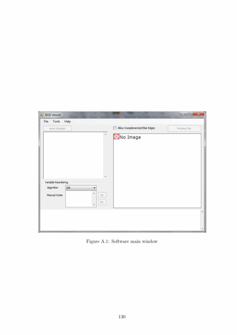
Figure A.1: Software main window
130

Figure A.2: Open file type pla or blif
131

Figure A.3: BDD variable reordering choices
Figure A.4: Tools menu
132

Figure A.5: Planar layout generation
Click ”Process File”. Dummy nodes will be created and inserted to make routing only
between adjacent levels. The log window will report the number of duplicated nodes required
and produce a planar BDD.
If you unselect the ”Connect to zero”, you will get an output similar to the one in
Figure A.6.
There are several options to export the generated layout as shown in Figure A.7. There
is a text description that can be mated to any of the popular tools, and it is possible to
export images. The number of images and their sizes are controlled by the grid size and the
bitmap width in the layout generation window.
For SPICE simulations,we launch the tool shown in Figure A.8 and supply a BDD node
133

Figure A.6: Planar layout without connections to a zero terminal
Figure A.7: Planar layout export options
134

description, an inverter description and a transistor models file.
The inverter description has to use the following node names: Nvdd, Nin, Nout.Example:
MQ1 Nvdd Nin Nout Nvdd pmosmodel (L=16nm)
MQ2 Nout Nin 0 0 nmosmodel (L=16nm)
The BDD node description has to use the following node names:
Nvdd, Ns, Ns_bar, Nin1, Nin2, Nout
. Example:
MQ1 Nin1 Ns Nout Nin1 nmosmodel (L=16nm)
MQ2 Nin1 Ns_bar Nout Nout pmosmodel (L=16nm)
MQ3 Nin2 Ns_bar Nout Nin2 nmosmodel (L=16nm)
MQ4 Nin2 Ns Nout Nout pmosmodel (L=16nm)
The transistor model file includes the model description for BSIM4 (Spice level 54).
The simulation window has the options to define complement signal in terms of inverters
or voltage sources or ignore them (short to ground) if a BDD node generates its own control
signal complement internally. The control signal grid allow the definition of constant or
periodic voltage sources with added noise. The absolute noise power is required as an input
in the grid. For a specific SNR, refer to the discussion on calculating the noise power. Click on
run simulation and this will launch Ngspice and simulate the circuit. The output log file will
be displayed in the tab called ”Sim Log”. To view the waveforms, there are two options. The
first option is to use the waveform plotter with the software. Click on the button ”waveform
plotter”. The second option is to use Matlab and the script ”ngspice.m”, included with this
software. This script will parse the Ngspice output and place corresponding variables in the
Matlab workspace.
135
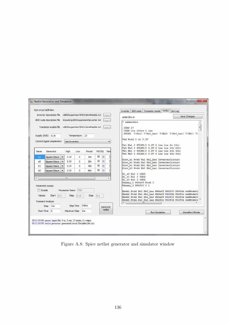
Figure A.8: Spice netlist generator and simulator window
136

Figure A.9: Error Correction PLA generation window
137

The third tool shown in Figure A.9 is the error correction generation tool. In this tool,
the diagram is analyzed to produce a complete truth table of the logic functions in the shared
diagram. A Hamming-code parity generator matrix is automatically created and truncated
if necessary in the case of shortened codes. Shortened codes are the Hamming codes that
do not satisfy the general rule for code length which is 2m − 1, 2m −m − 1 where m is the
number of parity bits. For example, the (5, 2) code used to encode two bits. It is possible
to edit the parity generator matrix before applying it. The tool will then generate a new
PLA file that describes the diagram with error correction. The number of inputs in the file
is increased due to the addition of the parity bits.
138

Appendix B
SPICE net listings for crossbar circuits
The following are SPICE net listings used in the simulations of the crossbar based nanocircuits.
Nano-adder
* source NANOADDER
V_VCp1 N226723 0 PWL TIME_SCALE_FACTOR=1e-8 VALUE_SCALE_FACTOR=1
+ REPEAT FOREVER
+ (1,15) (3.3,15)
+ (3.5,-7.5) (7,-7.5)
+ (7.5,5) (100,5)
+ ENDREPEAT
V_VCm0 N226742 0 PWL TIME_SCALE_FACTOR=1e-8 VALUE_SCALE_FACTOR=1
+ REPEAT FOREVER
+ (1,-15) (3.3,-15)
+ (3.5,12.5) (7,12.5)
+ (7.5,0) (100,0)
+ ENDREPEAT
V_Vx N226175 0
+PULSE 5 0 0 1n 1n 1u 2u
R_R1 0 N226983 100Meg
V_VCp0 N226777 0 PWL TIME_SCALE_FACTOR=1e-8 VALUE_SCALE_FACTOR=1
+ REPEAT FOREVER
+ (1,15) (3.3,15)
+ (3.5,-7.5) (7,-7.5)
+ (7.5,0) (100,0)
+ ENDREPEAT
V_VCm1 N226801 0 PWL TIME_SCALE_FACTOR=1e-8 VALUE_SCALE_FACTOR=1
+ REPEAT FOREVER
+ (1,-15) (3.3,-15)
+ (3.5,12.5) (7,12.5)
+ (7.5,5) (100,5)
+ ENDREPEAT
R_R2 0 N227012 100Meg
V_Vy N226179 0
+PULSE 5 0 0 1n 1n 2u 4u
D_Adder_D3 Adder_N01927 Adder_N00766 Dbreak
D_Adder_D15 Adder_N04509 Adder_N51462 Dbreak
D_Adder_D5 Adder_N01927 Adder_N84146 Dbreak
D_Adder_D12 Adder_N04325 N226983 Dbreak
D_Adder_D16 Adder_N04509 Adder_N09858 Dbreak
R_Adder_R4 Adder_N04325 VCC_BAR 100k
R_Adder_R9 0 N226983 1Meg
D_Adder_D9 Adder_N02599 Adder_N84146 Dbreak
R_Adder_R6 Adder_N04349 VCC_BAR 100k
D_Adder_D4 Adder_N00476 Adder_N51462 Dbreak
D_Adder_D14 Adder_N09474 N226983 Dbreak
R_Adder_R8 0 N227012 1Meg
D_Adder_D8 Adder_N02599 Adder_N51462 Dbreak
D_Adder_D20 Adder_N04325 Adder_N09858 Dbreak
D_Adder_D1 Adder_N00476 Adder_N00766 Dbreak
D_Adder_D7 Adder_N02599 N227012 Dbreak
D_Adder_D10 Adder_N01927 N227012 Dbreak
D_Adder_D13 Adder_N04349 N226983 Dbreak
D_Adder_D17 Adder_N04349 Adder_N33511 Dbreak
D_Adder_D37 Adder_N09474 Adder_N00766 Dbreak
R_Adder_R1 Adder_N00476 VCC_BAR 100k
D_Adder_D11 Adder_N04509 N226983 Dbreak
139

X_Adder_clatch6_S1 N226801 Adder_clatch6_N180534 N226801
+ Adder_clatch6_N175838 SCHEMATIC3_Adder_clatch6_S1
R_Adder_clatch6_R10 Adder_clatch6_N175838 Adder_N37004 1k
D_Adder_clatch6_D18 N226645 Adder_clatch6_N180534 Dbreak
C_Adder_clatch6_C1 0 Adder_N37004 10p
R_Adder_clatch6_R7 Adder_N37004 Adder_clatch6_N175820 1k
X_Adder_clatch6_S3 Adder_clatch6_N180534 N226777 Adder_clatch6_N175820
+ N226777 SCHEMATIC3_Adder_clatch6_S3
X_Adder_clatch5_S1 N226742 Adder_clatch5_N180534 N226742
+ Adder_clatch5_N175838 SCHEMATIC3_Adder_clatch5_S1
R_Adder_clatch5_R10 Adder_clatch5_N175838 Adder_N84146 1k
D_Adder_clatch5_D18 N226645 Adder_clatch5_N180534 Dbreak
C_Adder_clatch5_C1 0 Adder_N84146 10p
R_Adder_clatch5_R7 Adder_N84146 Adder_clatch5_N175820 1k
X_Adder_clatch5_S3 Adder_clatch5_N180534 N226723 Adder_clatch5_N175820
+ N226723 SCHEMATIC3_Adder_clatch5_S3
D_Adder_D22 Adder_N04325 Adder_N33511 Dbreak
X_Adder_clatch4_S1 N226801 Adder_clatch4_N180534 N226801
+ Adder_clatch4_N175838 SCHEMATIC3_Adder_clatch4_S1
R_Adder_clatch4_R10 Adder_clatch4_N175838 Adder_N33511 1k
D_Adder_clatch4_D18 N226179 Adder_clatch4_N180534 Dbreak
C_Adder_clatch4_C1 0 Adder_N33511 10p
R_Adder_clatch4_R7 Adder_N33511 Adder_clatch4_N175820 1k
X_Adder_clatch4_S3 Adder_clatch4_N180534 N226777 Adder_clatch4_N175820
+ N226777 SCHEMATIC3_Adder_clatch4_S3
X_Adder_clatch3_S1 N226742 Adder_clatch3_N180534 N226742
+ Adder_clatch3_N175838 SCHEMATIC3_Adder_clatch3_S1
R_Adder_clatch3_R10 Adder_clatch3_N175838 Adder_N51462 1k
D_Adder_clatch3_D18 N226179 Adder_clatch3_N180534 Dbreak
C_Adder_clatch3_C1 0 Adder_N51462 10p
R_Adder_clatch3_R7 Adder_N51462 Adder_clatch3_N175820 1k
X_Adder_clatch3_S3 Adder_clatch3_N180534 N226723 Adder_clatch3_N175820
+ N226723 SCHEMATIC3_Adder_clatch3_S3
D_Adder_D18 Adder_N09474 Adder_N51462 Dbreak
X_Adder_clatch2_S1 N226801 Adder_clatch2_N180534 N226801
+ Adder_clatch2_N175838 SCHEMATIC3_Adder_clatch2_S1
R_Adder_clatch2_R10 Adder_clatch2_N175838 Adder_N09858 1k
D_Adder_clatch2_D18 N226175 Adder_clatch2_N180534 Dbreak
C_Adder_clatch2_C1 0 Adder_N09858 10p
R_Adder_clatch2_R7 Adder_N09858 Adder_clatch2_N175820 1k
X_Adder_clatch2_S3 Adder_clatch2_N180534 N226777 Adder_clatch2_N175820
+ N226777 SCHEMATIC3_Adder_clatch2_S3
D_Adder_D19 Adder_N09474 Adder_N84146 Dbreak
X_Adder_clatch1_S1 N226742 Adder_clatch1_N180534 N226742
+ Adder_clatch1_N175838 SCHEMATIC3_Adder_clatch1_S1
R_Adder_clatch1_R10 Adder_clatch1_N175838 Adder_N00766 1k
D_Adder_clatch1_D18 N226175 Adder_clatch1_N180534 Dbreak
C_Adder_clatch1_C1 0 Adder_N00766 10p
R_Adder_clatch1_R7 Adder_N00766 Adder_clatch1_N175820 1k
X_Adder_clatch1_S3 Adder_clatch1_N180534 N226723 Adder_clatch1_N175820
+ N226723 SCHEMATIC3_Adder_clatch1_S3
D_Adder_D23 Adder_N04325 Adder_N84146 Dbreak
R_Adder_R2 Adder_N02599 VCC_BAR 100k
R_Adder_R3 Adder_N01927 VCC_BAR 100k
D_Adder_D35 Adder_N04509 Adder_N37004 Dbreak
D_Adder_D36 Adder_N04349 Adder_N37004 Dbreak
R_Adder_R5 Adder_N04509 VCC_BAR 100k
D_Adder_D6 Adder_N00476 N227012 Dbreak
D_Adder_D21 Adder_N04349 Adder_N00766 Dbreak
V_Adder_V1 VCC_BAR 0 5Vdc
R_Adder_R7 Adder_N09474 VCC_BAR 100k
V_Vz N226645 0
+PULSE 5 0 0 1n 1n 4u 8u
.subckt SCHEMATIC3_Adder_clatch6_S1 1 2 3 4
S_Adder_clatch6_S1 3 4 1 2 _Adder_clatch6_S1
RS_Adder_clatch6_S1 1 2 1G
.MODEL _Adder_clatch6_S1 VSWITCH Roff=1e6 Ron=1.0 VH=10 VT=0 TD=0
140

.ends SCHEMATIC3_Adder_clatch6_S1
.subckt SCHEMATIC3_Adder_clatch6_S3 1 2 3 4
S_Adder_clatch6_S3 3 4 1 2 _Adder_clatch6_S3
RS_Adder_clatch6_S3 1 2 1G
.MODEL _Adder_clatch6_S3 VSWITCH Roff=1e6 Ron=1.0 VH=10 VT=0 TD=0
.ends SCHEMATIC3_Adder_clatch6_S3
.subckt SCHEMATIC3_Adder_clatch5_S1 1 2 3 4
S_Adder_clatch5_S1 3 4 1 2 _Adder_clatch5_S1
RS_Adder_clatch5_S1 1 2 1G
.MODEL _Adder_clatch5_S1 VSWITCH Roff=1e6 Ron=1.0 VH=10 VT=0 TD=0
.ends SCHEMATIC3_Adder_clatch5_S1
.subckt SCHEMATIC3_Adder_clatch5_S3 1 2 3 4
S_Adder_clatch5_S3 3 4 1 2 _Adder_clatch5_S3
RS_Adder_clatch5_S3 1 2 1G
.MODEL _Adder_clatch5_S3 VSWITCH Roff=1e6 Ron=1.0 VH=10 VT=0 TD=0
.ends SCHEMATIC3_Adder_clatch5_S3
.subckt SCHEMATIC3_Adder_clatch4_S1 1 2 3 4
S_Adder_clatch4_S1 3 4 1 2 _Adder_clatch4_S1
RS_Adder_clatch4_S1 1 2 1G
.MODEL _Adder_clatch4_S1 VSWITCH Roff=1e6 Ron=1.0 VH=10 VT=0 TD=0
.ends SCHEMATIC3_Adder_clatch4_S1
.subckt SCHEMATIC3_Adder_clatch4_S3 1 2 3 4
S_Adder_clatch4_S3 3 4 1 2 _Adder_clatch4_S3
RS_Adder_clatch4_S3 1 2 1G
.MODEL _Adder_clatch4_S3 VSWITCH Roff=1e6 Ron=1.0 VH=10 VT=0 TD=0
.ends SCHEMATIC3_Adder_clatch4_S3
.subckt SCHEMATIC3_Adder_clatch3_S1 1 2 3 4
S_Adder_clatch3_S1 3 4 1 2 _Adder_clatch3_S1
RS_Adder_clatch3_S1 1 2 1G
.MODEL _Adder_clatch3_S1 VSWITCH Roff=1e6 Ron=1.0 VH=10 VT=0 TD=0
.ends SCHEMATIC3_Adder_clatch3_S1
.subckt SCHEMATIC3_Adder_clatch3_S3 1 2 3 4
S_Adder_clatch3_S3 3 4 1 2 _Adder_clatch3_S3
RS_Adder_clatch3_S3 1 2 1G
.MODEL _Adder_clatch3_S3 VSWITCH Roff=1e6 Ron=1.0 VH=10 VT=0 TD=0
.ends SCHEMATIC3_Adder_clatch3_S3
.subckt SCHEMATIC3_Adder_clatch2_S1 1 2 3 4
S_Adder_clatch2_S1 3 4 1 2 _Adder_clatch2_S1
RS_Adder_clatch2_S1 1 2 1G
.MODEL _Adder_clatch2_S1 VSWITCH Roff=1e6 Ron=1.0 VH=10 VT=0 TD=0
.ends SCHEMATIC3_Adder_clatch2_S1
.subckt SCHEMATIC3_Adder_clatch2_S3 1 2 3 4
S_Adder_clatch2_S3 3 4 1 2 _Adder_clatch2_S3
RS_Adder_clatch2_S3 1 2 1G
.MODEL _Adder_clatch2_S3 VSWITCH Roff=1e6 Ron=1.0 VH=10 VT=0 TD=0
.ends SCHEMATIC3_Adder_clatch2_S3
.subckt SCHEMATIC3_Adder_clatch1_S1 1 2 3 4
S_Adder_clatch1_S1 3 4 1 2 _Adder_clatch1_S1
RS_Adder_clatch1_S1 1 2 1G
.MODEL _Adder_clatch1_S1 VSWITCH Roff=1e6 Ron=1.0 VH=10 VT=0 TD=0
.ends SCHEMATIC3_Adder_clatch1_S1
.subckt SCHEMATIC3_Adder_clatch1_S3 1 2 3 4
S_Adder_clatch1_S3 3 4 1 2 _Adder_clatch1_S3
RS_Adder_clatch1_S3 1 2 1G
.MODEL _Adder_clatch1_S3 VSWITCH Roff=1e6 Ron=1.0 VH=10 VT=0 TD=0
.ends SCHEMATIC3_Adder_clatch1_S3
141

4-1 nano Multiplexer
* source NANOADDER
.EXTERNAL INPUT A
.EXTERNAL INPUT B
.EXTERNAL INPUT C
.EXTERNAL INPUT D
.EXTERNAL INPUT S0
.EXTERNAL INPUT S1
.EXTERNAL INPUT VCm0
.EXTERNAL INPUT VCm1
.EXTERNAL INPUT VCp0
.EXTERNAL INPUT VCp1
.EXTERNAL OUTPUT Mux
D_D20 N258177 N258545 Dbreak
D_D3 N256495 N256357 Dbreak
D_D16 N256495 B Dbreak
D_D21 N256295 D Dbreak
D_D1 N256295 N256357 Dbreak
V_VCp1 N559517 0 PWL TIME_SCALE_FACTOR=1e-8 VALUE_SCALE_FACTOR=1
+ REPEAT FOREVER
+ (1,15) (3.3,15)
+ (3.5,-7.5) (7,-7.5)
+ (7.5,5) (100,5)
+ ENDREPEAT
D_D17 N258177 A Dbreak
V_Vz N559996 0
+PULSE 5 0 0 1n 1n 4u 8u
X_clatch1_S1 VCM0 clatch1_N180534 VCM0 clatch1_N175838 SCHEMATIC3_clatch1_S1
+
R_clatch1_R7 N256357 clatch1_N175820 1k
R_clatch1_R10 clatch1_N175838 N256357 1k
C_clatch1_C1 0 N256357 1n
D_clatch1_D18 S0 clatch1_N180534 Dbreak
X_clatch1_S3 clatch1_N180534 VCP1 clatch1_N175820 VCP1 SCHEMATIC3_clatch1_S3
+
V_VCm0 N559523 0 PWL TIME_SCALE_FACTOR=1e-8 VALUE_SCALE_FACTOR=1
+ REPEAT FOREVER
+ (1,-15) (3.3,-15)
+ (3.5,12.5) (7,12.5)
+ (7.5,0) (100,0)
+ ENDREPEAT
D_D8 N256535 N258555 Dbreak
D_D25 N258177 MUX Dbreak
X_clatch2_S1 VCM1 clatch2_N180534 VCM1 clatch2_N175838 SCHEMATIC3_clatch2_S1
+
R_clatch2_R7 N258545 clatch2_N175820 1k
R_clatch2_R10 clatch2_N175838 N258545 1k
C_clatch2_C1 0 N258545 1n
D_clatch2_D18 S0 clatch2_N180534 Dbreak
X_clatch2_S3 clatch2_N180534 VCP0 clatch2_N175820 VCP0 SCHEMATIC3_clatch2_S3
+
V_V1 VCC_BAR 0 5Vdc
V_Vx N559860 0
+PULSE 5 0 0 1n 1n 1u 2u
D_D14 N258177 N258583 Dbreak
X_clatch3_S1 VCM0 clatch3_N180534 VCM0 clatch3_N175838 SCHEMATIC3_clatch3_S1
+
R_clatch3_R7 N258555 clatch3_N175820 1k
R_clatch3_R10 clatch3_N175838 N258555 1k
C_clatch3_C1 0 N258555 1n
D_clatch3_D18 S1 clatch3_N180534 Dbreak
X_clatch3_S3 clatch3_N180534 VCP1 clatch3_N175820 VCP1 SCHEMATIC3_clatch3_S3
142

+
V_VCp0 N559529 0 PWL TIME_SCALE_FACTOR=1e-8 VALUE_SCALE_FACTOR=1
+ REPEAT FOREVER
+ (1,15) (3.3,15)
+ (3.5,-7.5) (7,-7.5)
+ (7.5,0) (100,0)
+ ENDREPEAT
X_clatch4_S1 VCM1 clatch4_N180534 VCM1 clatch4_N175838 SCHEMATIC3_clatch4_S1
+
R_clatch4_R7 N258583 clatch4_N175820 1k
R_clatch4_R10 clatch4_N175838 N258583 1k
C_clatch4_C1 0 N258583 1n
D_clatch4_D18 S1 clatch4_N180534 Dbreak
X_clatch4_S3 clatch4_N180534 VCP0 clatch4_N175820 VCP0 SCHEMATIC3_clatch4_S3
+
D_D13 N256495 N258583 Dbreak
D_D24 N256495 MUX Dbreak
D_D4 N256295 N258555 Dbreak
V_VCm1 N559535 0 PWL TIME_SCALE_FACTOR=1e-8 VALUE_SCALE_FACTOR=1
+ REPEAT FOREVER
+ (1,-15) (3.3,-15)
+ (3.5,12.5) (7,12.5)
+ (7.5,5) (100,5)
+ ENDREPEAT
R_R1 N256295 VCC_BAR 100k
R_R3 N256495 VCC_BAR 100k
D_D23 N256535 MUX Dbreak
R_R4 N258177 VCC_BAR 100k
D_D12 N256535 N258545 Dbreak
R_R2 N256535 VCC_BAR 100k
R_R8 0 MUX 1Meg
V_Vy N559866 0
+PULSE 5 0 0 1n 1n 2u 4u
D_D22 N256295 MUX Dbreak
D_D15 N256535 C Dbreak
.subckt SCHEMATIC3_clatch1_S1 1 2 3 4
S_clatch1_S1 3 4 1 2 _clatch1_S1
RS_clatch1_S1 1 2 1G
.MODEL _clatch1_S1 VSWITCH Roff=1e6 Ron=1.0 VH=10 VT=0 TD=0
.ends SCHEMATIC3_clatch1_S1
.subckt SCHEMATIC3_clatch1_S3 1 2 3 4
S_clatch1_S3 3 4 1 2 _clatch1_S3
RS_clatch1_S3 1 2 1G
.MODEL _clatch1_S3 VSWITCH Roff=1e6 Ron=1.0 VH=10 VT=0 TD=0
.ends SCHEMATIC3_clatch1_S3
.subckt SCHEMATIC3_clatch2_S1 1 2 3 4
S_clatch2_S1 3 4 1 2 _clatch2_S1
RS_clatch2_S1 1 2 1G
.MODEL _clatch2_S1 VSWITCH Roff=1e6 Ron=1.0 VH=10 VT=0 TD=0
.ends SCHEMATIC3_clatch2_S1
.subckt SCHEMATIC3_clatch2_S3 1 2 3 4
S_clatch2_S3 3 4 1 2 _clatch2_S3
RS_clatch2_S3 1 2 1G
.MODEL _clatch2_S3 VSWITCH Roff=1e6 Ron=1.0 VH=10 VT=0 TD=0
.ends SCHEMATIC3_clatch2_S3
.subckt SCHEMATIC3_clatch3_S1 1 2 3 4
S_clatch3_S1 3 4 1 2 _clatch3_S1
RS_clatch3_S1 1 2 1G
.MODEL _clatch3_S1 VSWITCH Roff=1e6 Ron=1.0 VH=10 VT=0 TD=0
.ends SCHEMATIC3_clatch3_S1
.subckt SCHEMATIC3_clatch3_S3 1 2 3 4
S_clatch3_S3 3 4 1 2 _clatch3_S3
143

RS_clatch3_S3 1 2 1G
.MODEL _clatch3_S3 VSWITCH Roff=1e6 Ron=1.0 VH=10 VT=0 TD=0
.ends SCHEMATIC3_clatch3_S3
.subckt SCHEMATIC3_clatch4_S1 1 2 3 4
S_clatch4_S1 3 4 1 2 _clatch4_S1
RS_clatch4_S1 1 2 1G
.MODEL _clatch4_S1 VSWITCH Roff=1e6 Ron=1.0 VH=10 VT=0 TD=0
.ends SCHEMATIC3_clatch4_S1
.subckt SCHEMATIC3_clatch4_S3 1 2 3 4
S_clatch4_S3 3 4 1 2 _clatch4_S3
RS_clatch4_S3 1 2 1G
.MODEL _clatch4_S3 VSWITCH Roff=1e6 Ron=1.0 VH=10 VT=0 TD=0
.ends SCHEMATIC3_clatch4_S3
.model Dbreak d
+ is=1e-006
+ cjo=1e-013
+ rs=0.1
+ vj=0.2
Shift Register
* source NANOADDER
X_clatch1_S1 N226983 clatch1_N180534 N226983 clatch1_N175838
+ SCHEMATIC3_clatch1_S1
R_clatch1_R10 clatch1_N175838 N232294 1k
D_clatch1_D18 N227088 clatch1_N180534 Dbreak
C_clatch1_C1 0 N232294 10p
R_clatch1_R7 N232294 clatch1_N175820 1k
X_clatch1_S3 clatch1_N180534 N228190 clatch1_N175820 N228190
+ SCHEMATIC3_clatch1_S3
X_clatch4_S1 N227267 clatch4_N180534 N227267 clatch4_N175838
+ SCHEMATIC3_clatch4_S1
R_clatch4_R10 clatch4_N175838 N229783 1k
D_clatch4_D18 N238779 clatch4_N180534 Dbreak
C_clatch4_C1 0 N229783 10p
R_clatch4_R7 N229783 clatch4_N175820 1k
X_clatch4_S3 clatch4_N180534 N227279 clatch4_N175820 N227279
+ SCHEMATIC3_clatch4_S3
V_Vx N227088 0
+PULSE 5 0 0 1n 1n 2u 3u
R_R5 0 N229783 100k
V_VCp11 N228190 0 PWL TIME_SCALE_FACTOR=1e-8 VALUE_SCALE_FACTOR=1
+ REPEAT FOREVER
+ (1,15) (3.3,15)
+ (3.5,-7.5) (7,-7.5)
+ (7.5,5) (100,5)
+ ENDREPEAT
V_VCm01 N226983 0 PWL TIME_SCALE_FACTOR=1e-8 VALUE_SCALE_FACTOR=1
+ REPEAT FOREVER
+ (1,-15) (3.3,-15)
+ (3.5,12.5) (7,12.5)
+ (7.5,0) (100,0)
+ ENDREPEAT
X_clatch2_S1 N227267 clatch2_N180534 N227267 clatch2_N175838
+ SCHEMATIC3_clatch2_S1
R_clatch2_R10 clatch2_N175838 N239754 1k
D_clatch2_D18 N232294 clatch2_N180534 Dbreak
C_clatch2_C1 0 N239754 10p
R_clatch2_R7 N239754 clatch2_N175820 1k
X_clatch2_S3 clatch2_N180534 N227279 clatch2_N175820 N227279
144

+ SCHEMATIC3_clatch2_S3
V_VCp12 N227279 0 PWL TIME_SCALE_FACTOR=1e-8 VALUE_SCALE_FACTOR=1
+ REPEAT FOREVER
+ (50,5) (51,15) (53.3,15)
+ (53.5,-7.5) (57,-7.5)
+ (57.5,5) (100,5)
+ ENDREPEAT
V_VCm02 N227267 0 PWL TIME_SCALE_FACTOR=1e-8 VALUE_SCALE_FACTOR=1
+ REPEAT FOREVER
+ (50,0) (51,-15) (53.3,-15)
+ (53.5,12.5) (57,12.5)
+ (57.5,0) (100,0)
+ ENDREPEAT
X_clatch3_S1 N226983 clatch3_N180534 N226983 clatch3_N175838
+ SCHEMATIC3_clatch3_S1
R_clatch3_R10 clatch3_N175838 N238779 1k
D_clatch3_D18 N239754 clatch3_N180534 Dbreak
C_clatch3_C1 0 N238779 10p
R_clatch3_R7 N238779 clatch3_N175820 1k
X_clatch3_S3 clatch3_N180534 N228190 clatch3_N175820 N228190
+ SCHEMATIC3_clatch3_S3
.subckt SCHEMATIC3_clatch1_S1 1 2 3 4
S_clatch1_S1 3 4 1 2 _clatch1_S1
RS_clatch1_S1 1 2 1G
.MODEL _clatch1_S1 VSWITCH Roff=1e6 Ron=1.0 VH=10 VT=0 TD=0
.ends SCHEMATIC3_clatch1_S1
.subckt SCHEMATIC3_clatch1_S3 1 2 3 4
S_clatch1_S3 3 4 1 2 _clatch1_S3
RS_clatch1_S3 1 2 1G
.MODEL _clatch1_S3 VSWITCH Roff=1e6 Ron=1.0 VH=10 VT=0 TD=0
.ends SCHEMATIC3_clatch1_S3
.subckt SCHEMATIC3_clatch4_S1 1 2 3 4
S_clatch4_S1 3 4 1 2 _clatch4_S1
RS_clatch4_S1 1 2 1G
.MODEL _clatch4_S1 VSWITCH Roff=1e6 Ron=1.0 VH=10 VT=0 TD=0
.ends SCHEMATIC3_clatch4_S1
.subckt SCHEMATIC3_clatch4_S3 1 2 3 4
S_clatch4_S3 3 4 1 2 _clatch4_S3
RS_clatch4_S3 1 2 1G
.MODEL _clatch4_S3 VSWITCH Roff=1e6 Ron=1.0 VH=10 VT=0 TD=0
.ends SCHEMATIC3_clatch4_S3
.subckt SCHEMATIC3_clatch2_S1 1 2 3 4
S_clatch2_S1 3 4 1 2 _clatch2_S1
RS_clatch2_S1 1 2 1G
.MODEL _clatch2_S1 VSWITCH Roff=1e6 Ron=1.0 VH=10 VT=0 TD=0
.ends SCHEMATIC3_clatch2_S1
.subckt SCHEMATIC3_clatch2_S3 1 2 3 4
S_clatch2_S3 3 4 1 2 _clatch2_S3
RS_clatch2_S3 1 2 1G
.MODEL _clatch2_S3 VSWITCH Roff=1e6 Ron=1.0 VH=10 VT=0 TD=0
.ends SCHEMATIC3_clatch2_S3
.subckt SCHEMATIC3_clatch3_S1 1 2 3 4
S_clatch3_S1 3 4 1 2 _clatch3_S1
RS_clatch3_S1 1 2 1G
.MODEL _clatch3_S1 VSWITCH Roff=1e6 Ron=1.0 VH=10 VT=0 TD=0
.ends SCHEMATIC3_clatch3_S1
.subckt SCHEMATIC3_clatch3_S3 1 2 3 4
S_clatch3_S3 3 4 1 2 _clatch3_S3
RS_clatch3_S3 1 2 1G
.MODEL _clatch3_S3 VSWITCH Roff=1e6 Ron=1.0 VH=10 VT=0 TD=0
145

.ends SCHEMATIC3_clatch3_S3
Toggle T-flipflop
* source T-flipflop
.EXTERNAL OUTPUT Qo
.EXTERNAL INPUT Toggle
V_VCp4 VCP1Q 0 PWL TIME_SCALE_FACTOR=1e-7 VALUE_SCALE_FACTOR=1
+ REPEAT FOREVER
+ (50,5) (51,15) (53.3,15)
+ (53.5,-7.5) (57,-7.5)
+ (57.5,5) (100,5)
+ ENDREPEAT
R_R3 0 QO 1MEG
V_VCm4 VCM0Q 0 PWL TIME_SCALE_FACTOR=1e-7 VALUE_SCALE_FACTOR=1
+ REPEAT FOREVER
+ (50,0)(51,-15) (53.3,-15)
+ (53.5,12.5) (57,12.5)
+ (57.5,0) (100,0)
+ ENDREPEAT
D_D8 N229934 N413328 Dbreak
V_VCp2 VCP1T 0 PWL TIME_SCALE_FACTOR=1e-7 VALUE_SCALE_FACTOR=1
+ REPEAT FOREVER
+ (1,15) (3.3,15)
+ (3.5,-7.5) (7,-7.5)
+ (7.5,5) (100,5)
+ ENDREPEAT
V_VCp5 VCP0Q 0 PWL TIME_SCALE_FACTOR=1e-7 VALUE_SCALE_FACTOR=1
+ REPEAT FOREVER
+ (50,0) (51,15) (53.3,15)
+ (53.5,-7.5) (57,-7.5)
+ (57.5,0) (100,0)
+ ENDREPEAT
V_VCm2 VCM0T 0 PWL TIME_SCALE_FACTOR=1e-7 VALUE_SCALE_FACTOR=1
+ REPEAT FOREVER
+ (1,-15) (3.3,-15)
+ (3.5,12.5) (7,12.5)
+ (7.5,0) (100,0)
+ ENDREPEAT
V_VCm5 VCM1Q 0 PWL TIME_SCALE_FACTOR=1e-7 VALUE_SCALE_FACTOR=1
+ REPEAT FOREVER
+ (50,5)(51,-15) (53.3,-15)
+ (53.5,12.5) (57,12.5)
+ (57.5,5) (100,5)
+ ENDREPEAT
D_D9 N229934 N229624 Dbreak
D_D11 N229934 QO Dbreak
V_VCp3 VCP0T 0 PWL TIME_SCALE_FACTOR=1e-7 VALUE_SCALE_FACTOR=1
+ REPEAT FOREVER
+ (1,15) (3.3,15)
+ (3.5,-7.5) (7,-7.5)
+ (7.5,0) (100,0)
+ ENDREPEAT
D_D1 N229644 N292674 Dbreak
V_VCm3 VCM1T 0 PWL TIME_SCALE_FACTOR=1e-7 VALUE_SCALE_FACTOR=1
+ REPEAT FOREVER
+ (1,-15) (1.3,-15)
+ (3.5,12.5) (7,12.5)
+ (7.5,5) (100,5)
+ ENDREPEAT
X_clatch3_S1 VCM0T clatch3_N180534 VCM0T clatch3_N175838
+ SCHEMATIC3_clatch3_S1
R_clatch3_R10 clatch3_N175838 N258593 1k
D_clatch3_D18 N258563 clatch3_N180534 Dbreak
146

C_clatch3_C1 0 N258593 1n
R_clatch3_R7 N258593 clatch3_N175820 1k
X_clatch3_S3 clatch3_N180534 VCP1T clatch3_N175820 VCP1T
+ SCHEMATIC3_clatch3_S3
D_D4 N229644 N258593 Dbreak
R_R1 N229644 VCC_BAR 10K
C_C1 0 QO 1P
R_R2 N229934 VCC_BAR 10K
D_D10 N229644 QO Dbreak
X_clatch5_S1 VCM0Q clatch5_N180534 VCM0Q clatch5_N175838
+ SCHEMATIC3_clatch5_S1
R_clatch5_R10 clatch5_N175838 N258563 1k
D_clatch5_D18 N638755 clatch5_N180534 Dbreak
C_clatch5_C1 0 N258563 1n
R_clatch5_R7 N258563 clatch5_N175820 1k
X_clatch5_S3 clatch5_N180534 VCP1Q clatch5_N175820 VCP1Q
+ SCHEMATIC3_clatch5_S3
R_R4 QO N6349720 1k
X_clatch4_S1 VCM1T clatch4_N180534 VCM1T clatch4_N175838
+ SCHEMATIC3_clatch4_S1
R_clatch4_R10 clatch4_N175838 N413328 1k
D_clatch4_D18 N258563 clatch4_N180534 Dbreak
C_clatch4_C1 0 N413328 1n
R_clatch4_R7 N413328 clatch4_N175820 1k
X_clatch4_S3 clatch4_N180534 VCP0T clatch4_N175820 VCP0T
+ SCHEMATIC3_clatch4_S3
V_Vx TOGGLE 0
+PULSE 0 5 50u 1n 1n 8u 50u
X_clatch1_S1 VCM0T clatch1_N180534 VCM0T clatch1_N175838
+ SCHEMATIC3_clatch1_S1
R_clatch1_R10 clatch1_N175838 N229624 1k
D_clatch1_D18 TOGGLE clatch1_N180534 Dbreak
C_clatch1_C1 0 N229624 1n
R_clatch1_R7 N229624 clatch1_N175820 1k
X_clatch1_S3 clatch1_N180534 VCP1T clatch1_N175820 VCP1T
+ SCHEMATIC3_clatch1_S3
D_D12 N6349720 N638755 Dbreak
V_V1 VCC_BAR 0 5Vdc
X_clatch2_S1 VCM1T clatch2_N180534 VCM1T clatch2_N175838
+ SCHEMATIC3_clatch2_S1
R_clatch2_R10 clatch2_N175838 N292674 1k
D_clatch2_D18 TOGGLE clatch2_N180534 Dbreak
C_clatch2_C1 0 N292674 1n
R_clatch2_R7 N292674 clatch2_N175820 1k
X_clatch2_S3 clatch2_N180534 VCP0T clatch2_N175820 VCP0T
+ SCHEMATIC3_clatch2_S3
.subckt SCHEMATIC3_clatch3_S1 1 2 3 4
S_clatch3_S1 3 4 1 2 _clatch3_S1
RS_clatch3_S1 1 2 1G
.MODEL _clatch3_S1 VSWITCH Roff=1e6 Ron=1.0 VH=10 VT=0 TD=0
.ends SCHEMATIC3_clatch3_S1
.subckt SCHEMATIC3_clatch3_S3 1 2 3 4
S_clatch3_S3 3 4 1 2 _clatch3_S3
RS_clatch3_S3 1 2 1G
.MODEL _clatch3_S3 VSWITCH Roff=1e6 Ron=1.0 VH=10 VT=0 TD=0
.ends SCHEMATIC3_clatch3_S3
.subckt SCHEMATIC3_clatch5_S1 1 2 3 4
S_clatch5_S1 3 4 1 2 _clatch5_S1
RS_clatch5_S1 1 2 1G
.MODEL _clatch5_S1 VSWITCH Roff=1e6 Ron=1.0 VH=10 VT=0 TD=0
.ends SCHEMATIC3_clatch5_S1
.subckt SCHEMATIC3_clatch5_S3 1 2 3 4
S_clatch5_S3 3 4 1 2 _clatch5_S3
RS_clatch5_S3 1 2 1G
147

.MODEL _clatch5_S3 VSWITCH Roff=1e6 Ron=1.0 VH=10 VT=0 TD=0
.ends SCHEMATIC3_clatch5_S3
.subckt SCHEMATIC3_clatch4_S1 1 2 3 4
S_clatch4_S1 3 4 1 2 _clatch4_S1
RS_clatch4_S1 1 2 1G
.MODEL _clatch4_S1 VSWITCH Roff=1e6 Ron=1.0 VH=10 VT=0 TD=0
.ends SCHEMATIC3_clatch4_S1
.subckt SCHEMATIC3_clatch4_S3 1 2 3 4
S_clatch4_S3 3 4 1 2 _clatch4_S3
RS_clatch4_S3 1 2 1G
.MODEL _clatch4_S3 VSWITCH Roff=1e6 Ron=1.0 VH=10 VT=0 TD=0
.ends SCHEMATIC3_clatch4_S3
.subckt SCHEMATIC3_clatch1_S1 1 2 3 4
S_clatch1_S1 3 4 1 2 _clatch1_S1
RS_clatch1_S1 1 2 1G
.MODEL _clatch1_S1 VSWITCH Roff=1e6 Ron=1.0 VH=10 VT=0 TD=0
.ends SCHEMATIC3_clatch1_S1
.subckt SCHEMATIC3_clatch1_S3 1 2 3 4
S_clatch1_S3 3 4 1 2 _clatch1_S3
RS_clatch1_S3 1 2 1G
.MODEL _clatch1_S3 VSWITCH Roff=1e6 Ron=1.0 VH=10 VT=0 TD=0
.ends SCHEMATIC3_clatch1_S3
.subckt SCHEMATIC3_clatch2_S1 1 2 3 4
S_clatch2_S1 3 4 1 2 _clatch2_S1
RS_clatch2_S1 1 2 1G
.MODEL _clatch2_S1 VSWITCH Roff=1e6 Ron=1.0 VH=10 VT=0 TD=0
.ends SCHEMATIC3_clatch2_S1
.subckt SCHEMATIC3_clatch2_S3 1 2 3 4
S_clatch2_S3 3 4 1 2 _clatch2_S3
RS_clatch2_S3 1 2 1G
.MODEL _clatch2_S3 VSWITCH Roff=1e6 Ron=1.0 VH=10 VT=0 TD=0
.ends SCHEMATIC3_clatch2_S3
148

Appendix C
Matlab code for the simulations
BDD node and TMR error correcting BDD node
function y=bddnode(s,x0,x1)
if s==1
y=x1;
else
y=x0;
end
function y=ecbddnode(p1,p0,s,x0,x1)
cs = [p1 p0 s];
n1out = bddnode(cs(1),x0,x1);
n2out = bddnode(cs(2),x0,n1out);
n3out = bddnode(cs(2),n1out,x1);
n4out = bddnode(cs(3),n2out,n3out);
y=n4out;
Reliability Simulation of Error Correcting 2x2 Adder
%test reliability of EC-adder
clear,clc,close all
m=3; % n=2^m-1, k=n-m, parity bits=m
[h,g,n,k] = hammgen(m);
b=(0:3)’;
addersum = [];
inputmat=double(dec2bin((0:2^k-1)’))-’0’;
for a=0:3
addersum = [addersum;a+b];
end
outputvector=dec2bin(addersum)-’0’;
inputvectors=mod(inputmat(:,:)*g,2);
%%
%error analysis
niterations = 500;
p=0.0:0.05:0.5;
ecreliability=zeros(length(p),3);
xx = rand(n,niterations);
for kp = 1:length(p)
disp(p(kp));
nerrors = [0 0 0];
for kit = 1:niterations
sigerror = xx(:,kit)<=p(kp);
for kinp=1:2^k
inval=xor(inputvectors(kinp,:),sigerror’);
msg = decode(inval,n,k,’hamming’);
%nout = [-1 -1 -1];
nout=outputvector(1+bin2dec(char(msg+’0’)),:);
nerrors = nerrors+(nout~=outputvector(kinp,:));
149

end
end
ecreliability(kp,:) = 1-nerrors/niterations/2^k;
end
%% test TMR using ecbddnode
tmreliability=zeros(length(p),3);
xx = rand(k*3,niterations);
for kp = 1:length(p)
disp(p(kp));
nerrors = [0 0 0];
for kit = 1:niterations
sigerror = xx(:,kit)<=p(kp);
for kinp=1:2^k
inval=xor([inputmat(kinp,1),inputmat(kinp,1),inputmat(kinp,1),...
inputmat(kinp,2),inputmat(kinp,2),inputmat(kinp,2),...
inputmat(kinp,3),inputmat(kinp,3),inputmat(kinp,3),...
inputmat(kinp,4),inputmat(kinp,4),inputmat(kinp,4)],sigerror’);
n1=ecbddnode(inval(10),inval(11),inval(12),0,1);
n22=n1;
n6=ecbddnode(inval(10),inval(11),inval(12),1,0);
n23=n6;
n2=ecbddnode(inval(4),inval(5),inval(6),0,n1);
n20=n2;
n7=ecbddnode(inval(4),inval(5),inval(6),1,n6);
n19=n2;
n11=ecbddnode(inval(4),inval(5),inval(6),n22,n23);
n3=ecbddnode(inval(7),inval(8),inval(9),n2,1);
n4=ecbddnode(inval(7),inval(8),inval(9),0,n2);
n8=ecbddnode(inval(7),inval(8),inval(9),n7,n20);
n9=ecbddnode(inval(7),inval(8),inval(9),n19,n7);
n5=ecbddnode(inval(1),inval(2),inval(3),n4,n3);
n10=ecbddnode(inval(1),inval(2),inval(3),n9,n8);
nout=[n5 n10 n11];
nerrors = nerrors+(nout~=outputvector(kinp,:));
%if nout~=outputvector(kinp);
% nerrors = nerrors+1;
%end
end
end
tmreliability(kp,:) = 1-nerrors/niterations/2^k;
end
%%
noecreliability=zeros(length(p),3);
xx = rand(k,niterations);
for kp = 1:length(p)
disp(p(kp));
nerrors = [0 0 0];
for kit = 1:niterations
sigerror = xx(:,kit)<=p(kp);
for kinp=1:2^k
inval=xor(inputmat(kinp,:),sigerror’);
n1=bddnode(inval(4),0,1);
n22=n1;
n6=bddnode(inval(4),1,0);
n23=n6;
n2=bddnode(inval(2),0,n1);
n20=n2;
n7=bddnode(inval(2),1,n6);
n19=n2;
n11=bddnode(inval(2),n22,n23);
n3=bddnode(inval(3),n2,1);
n4=bddnode(inval(3),0,n2);
n8=bddnode(inval(3),n7,n20);
n9=bddnode(inval(3),n19,n7);
n5=bddnode(inval(1),n4,n3);
150
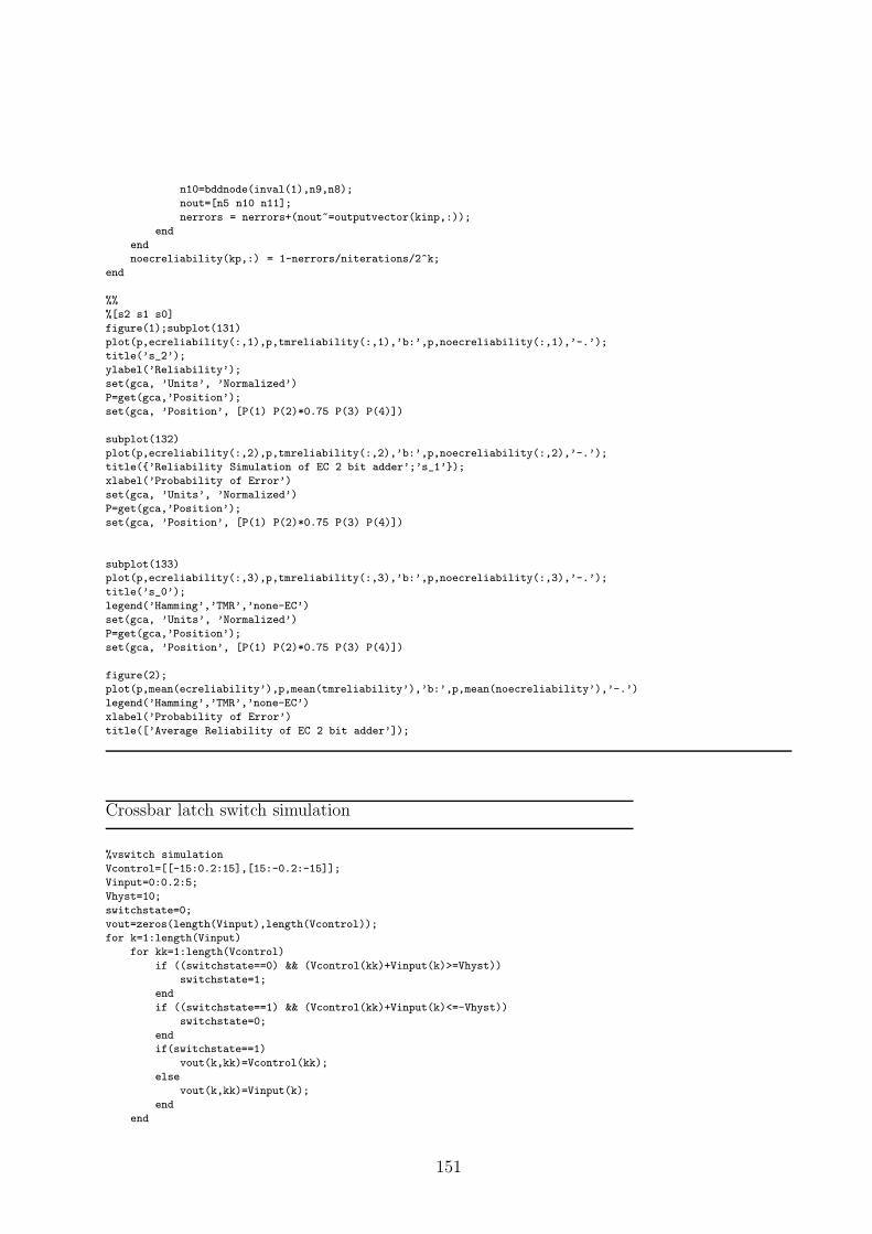
n10=bddnode(inval(1),n9,n8);
nout=[n5 n10 n11];
nerrors = nerrors+(nout~=outputvector(kinp,:));
end
end
noecreliability(kp,:) = 1-nerrors/niterations/2^k;
end
%%
%[s2 s1 s0]
figure(1);subplot(131)
plot(p,ecreliability(:,1),p,tmreliability(:,1),’b:’,p,noecreliability(:,1),’-.’);
title(’s_2’);
ylabel(’Reliability’);
set(gca, ’Units’, ’Normalized’)
P=get(gca,’Position’);
set(gca, ’Position’, [P(1) P(2)*0.75 P(3) P(4)])
subplot(132)
plot(p,ecreliability(:,2),p,tmreliability(:,2),’b:’,p,noecreliability(:,2),’-.’);
title(’Reliability Simulation of EC 2 bit adder’;’s_1’);
xlabel(’Probability of Error’)
set(gca, ’Units’, ’Normalized’)
P=get(gca,’Position’);
set(gca, ’Position’, [P(1) P(2)*0.75 P(3) P(4)])
subplot(133)
plot(p,ecreliability(:,3),p,tmreliability(:,3),’b:’,p,noecreliability(:,3),’-.’);
title(’s_0’);
legend(’Hamming’,’TMR’,’none-EC’)
set(gca, ’Units’, ’Normalized’)
P=get(gca,’Position’);
set(gca, ’Position’, [P(1) P(2)*0.75 P(3) P(4)])
figure(2);
plot(p,mean(ecreliability’),p,mean(tmreliability’),’b:’,p,mean(noecreliability’),’-.’)
legend(’Hamming’,’TMR’,’none-EC’)
xlabel(’Probability of Error’)
title([’Average Reliability of EC 2 bit adder’]);
Crossbar latch switch simulation
%vswitch simulation
Vcontrol=[[-15:0.2:15],[15:-0.2:-15]];
Vinput=0:0.2:5;
Vhyst=10;
switchstate=0;
vout=zeros(length(Vinput),length(Vcontrol));
for k=1:length(Vinput)
for kk=1:length(Vcontrol)
if ((switchstate==0) && (Vcontrol(kk)+Vinput(k)>=Vhyst))
switchstate=1;
end
if ((switchstate==1) && (Vcontrol(kk)+Vinput(k)<=-Vhyst))
switchstate=0;
end
if(switchstate==1)
vout(k,kk)=Vcontrol(kk);
else
vout(k,kk)=Vinput(k);
end
end
151

end
surf(Vcontrol,Vinput,vout);
colormap hsv
xlabel(’Control Voltage’);
ylabel(’Input signal’);
zlabel(’Output signal’)
colorbar
Representation of a complex number using algebraic integers
close all, clc, clear
for R = 4:4:12;
nvars = floor(R/2);
wj = exp(2*pi*j/R*[0:nvars-1]);
airange = -2:2;
ais = ones(1,nvars)*min(airange);
cnumbers = zeros(1,length(airange)^nvars);
counter=1;
while ais(nvars)<=max(airange);
cnumbers(counter)=sum(ais.*wj);
counter=counter+1;
ais(1)= ais(1)+1;
for k=1:nvars-1
if ais(k)>max(airange)
ais(k)=min(airange);
ais(k+1)=ais(k+1)+1;
end
end
end
figure;plot(real(cnumbers),imag(cnumbers),’.’)
title([’R=’,num2str(R),’ variables=’,num2str(nvars)]);
xlabel(’Real part’); ylabel(’Imaginary part’);
end
Calculating the Quantum Fourier Transform (QFT) of 3 Qubits
%quantum simulation of 3 bit QFT
clc
h=hadamard(2)/sqrt(2);
p0=[1 0]’;
p1=[0 1]’;
cnot=[eye(2),zeros(2);zeros(2),1-eye(2)]; %4by4
toffoli=[eye(6),zeros(6,2);zeros(2,6),1-eye(2)]; %8by8
cR2=[eye(3),zeros(3,1);zeros(1,3),i]; %4by4
cR3=[eye(3),zeros(3,1);zeros(1,3),sqrt(i)]; %4by4
%%%Set inputs
nqubits=3;
nops=6; %number of operations
qbits=zeros(2,1,nqubits);
qbits(:,:,1)=p0;
qbits(:,:,2)=p1;
qbits(:,:,3)=p0;
qops=zeros(2^nqubits,2^nqubits,nops);
qops(:,:,1)=kron(kron(h,eye(2)),eye(2));
qops(:,:,2)=kron(cR2,eye(2));
qops(:,:,3)=kron(cR3,eye(2));
qops(:,5:6,3)=qops(:,6:-1:5,3);
qops(5:6,:,3)=qops(6:-1:5,:,3);
152

qops(:,:,4)=kron(kron(eye(2),h),eye(2));
qops(:,:,5)=kron(eye(2),cR2);
qops(:,:,6)=kron(kron(eye(2),eye(2)),h);
systemstate=1;
for k=1:nqubits
systemstate=kron(systemstate,qbits(:,:,k)); %initial system state
end
for k=1:nops
systemstate=[systemstate,qops(:,:,k)*systemstate(:,end)];
end
systemstate
imagesc(abs(systemstate.^2))
colormap(1- gray)
set(gca,’XTick’,[0:nops+1],’XTickLabel’,[-1:nops],...
’YTick’,[0:2^nqubits],’YTickLabel’,dec2bin([-1:2^nqubits-1]));
xlabel(’computation step’);
ylabel(’quantum state’);
title(’absolute probabilities’)
153

Bibliography
[1] Carbon nanotubes & buckyballs. http://education.mrsec.wisc.edu/nanoquest/
carbon/index.html. [Online; accessed December 2010].
[2] National nanotechnology initiative. http://www.nano.gov/. [Online; accessed March
2012].
[3] A. Abdollahi. Probabilistic decision diagrams for exact probabilistic analysis. In Proc.
IEEE Int. Conference on Computer-Aided Design. ICCAD, pages 266–272, 2007.
[4] E. Ahmed and J. Rose. The effect of LUT and cluster size on deep-submicron FPGA
performance and density. IEEE Transactions on VLSI Systems, 12:288, 2004.
[5] M. A. Amiri, M. Mahdavi, and S. Mirzakuchaki. QCA implementation of a MUX-
based FPGA CLB. In Proc. Int. Conference on Nanoscience and Nanotechnology.
ICONN, 2008.
[6] M Andrecut. Stochastic recovery of sparse signals from random measurements. Engi-
neering Letters, 19(1):1–6, 2011.
[7] H. Astolaa, S. Stankovic, and J. T. Astola. Error-correcting decision diagrams. In
Proc. 3rd Workshop on Information Theoretic Methods in Science and Engineering,
august 2010.
[8] H. Astolaa, S. Stankovic, and J. T. Astola. Error-correcting decision diagrams for
multiple-valued functions. In Proc. 41st IEEE Int. Symposium on Multiple-Valued
Logic. ISMVL, 2011.
[9] M. D. Austin et al. Fabrication of 5nm linewidth and 14nm pitch features by nanoim-
print lithography. Applied Physics Letters, 84:5299–5301, 2004.
154

[10] A. Avizienis et al. The STAR (self-testing and repairing) computer: An investigation
of the theory and practice of fault-tolerant computer design. IEEE Transactions on
Computers, 100(11):1312–1321, 1971.
[11] R. Bahar, J. Chen, and J. Mundy. A probabilistic-based design for nanoscale compu-
tation. Nano, quantum and molecular computing, pages 133–156, 2004.
[12] J-M. Baribeau, N. L. Rowell, and D. J. Lockwood. Self assembled Si1−xGex dots and
islands. In Motonari Adachi and David J. Lockwood, editors, Self-Organized Nanoscale
Materials. Springer, 2006.
[13] G. Bersuker, B. H. Lee, A. Korkin, and H. R. Huff. Novel dielectric materials for future
transistor generations. In A. Korkin, J. Labanowski, E. Gusev, and S. Luryi, editors,
Nanotechnology for Electronic Materials and Devices. Springer, 2007.
[14] J. Borghetti, G. S. Snider, P. J. Kuekes, J. Yang, D. R. Stewart, and R. S. Williams.
‘Memristive’ switches enable ‘stateful’ logic operations via material implication. Na-
ture, 464(7290):873–876, 2010.
[15] R. Brayton and A. Mishchenko. ABC: An academic industrial-strength verification
tool. In Computer Aided Verification, pages 24–40. Springer, 2010.
[16] R. E. Bryant. Graph-based algorithms for boolean functions manipulation. IEEE
Transactions on Computers, C-35(8):667–691, 1986.
[17] A. W. Burks. Essays on Cellular Automata. University of Illinois Press, 1970.
[18] A. Cao and C-K. Koh. Non-crossing OBDDs for mapping to regular circuit structures.
In Proc. 21st Int. Conference on Computer Design. ICCD, pages 338–343, 2003.
[19] A. Cao and C. K. Koh. Decomposition of BDDs with application to physical mapping
of regular ptl circuits. Int. Workshop for Logic Synthesis, 2004.
155
[20] G. F. Cerofolini and D. Mascolo. A hybrid route from CMOS to nano and molecular
electronics. In A. Korkin, J. Labanowski, E. Gusev, and S. Luryi, editors, Nanotech-
nology for Electronic Materials and Devices. Springer, 2007.
[21] A. Chaudhary, D. Z. Chen, K. Whitton, M. Niemier, and R. Ravichandran. Elim-
inating wire crossings for molecular quantum-dot cellular automata implementation.
In Proc. IEEE/ACM Int. conference on Computer-aided design, pages 565–571. IEEE
Computer Society, 2005.
[22] K. Chen, C-M. Li, Q. Zhang, Y-A. Chen, A. Goebel, S. Chen, A. Mair, and J-W. Pan.
Experimental realization of one-way quantum computing with two-photon four-qubit
cluster states. Phys. Rev. Lett., 99(12):120503, Sep 2007.
[23] Y. Chen et al. Nanoscale molecular-switch devices fabricated by imprint lithography.
Applied Physics Letters, 82:1610–1612, March 2003.
[24] M. R. Choudhury and K. Mohanram. Reliability analysis of logic circuits. IEEE
Transactions on Computer-Aided Design of Integrated Circuits and Systems, 28(3):392–
405, March 2009.
[25] M. Chrzanowska-jeske and A. Mishchenko. Synthesis for regularity using decision
diagrams. In Proc. IEEE Int. Symposium on Circuits and Systems. ISCAS, 2005.
[26] C. P. Collier, E. W. Wong, M. Belohradsky, F. M. Raymo, J. F. Stoddar, P. J. Kuekes,
R. S. Williams, and J. R. Heath. Electronically configurable molecular-based logic
gates. Science, 285:391–394, 2001.
[27] C. Constantinescu. Intermittent faults in VLSI circuits. In Proc. IEEE Workshop on
Silicon Errors in Logic-System Effects. Citeseer, 2007.
[28] W. B. Culbertson, R. Amerson, R. J. Carter, P. Kuekes, and G. Snider. Defect tol-
erance on the teramac custom computer. In Proc. 5th Annual IEEE Symposium on
156

Field-Programmable Custom Computing Machines, pages 116 –123, April 1997.
[29] W. J. Dally and B. Towels. Route packets, not wires: On-chip interconnection net-
works. In Proc. Design automation conference. DAC, 2001.
[30] S. Das, G. Rose, M. M. Ziegler, C. A. Picconatto, and J. C. Ellenbogen. Architec-
tures and simulations for nanoprocessor systems integrated on the molecular scale. In
G. Cuniberti, G. Fagas, and K. Richter, editors, Introducing Molecular Electronics.
Springer, 2005.
[31] A. DeHon. Array-based architecture for FET-based, nanoscale electronics. IEEE
TNANO, 2:23–32, 2003.
[32] A. DeHon. Nanowire-based programmable architectures. Emerging Technologies,
Computing Systems, 1(2):109–162, 2005.
[33] A. DeHon and K. Likharev. Hybrid CMOS/nanoelectronic digital circuits: Devices,
architectures, and design automation. In Proc. ICCAD, pages 375–382, 2005.
[34] A. DeHon and H. Naeimi. Seven strategies for tolerating highly defective fabrication.
Design & Test of Computers, 22(4):306–315, 2005.
[35] A. DeHon and M. J. Wilson. Nanowire-based sublithographic programmable logic
arrays. In Proc. ACM/SIGDA 12th Int. symposium on Field programmable gate arrays,
pages 123–132, 2004.
[36] C. Dong, W. Wang, and S. Haruehanroengra. Efficient logic architectures for CMOL
nanoelectronic circuits. Micro Nano Letters, IET, 1(2):74 –78, Dec 2006.
[37] D. L. Donoho. Compressed sensing. IEEE Transactions on Information Theory,
52(4):1289–1306, 2006.
157

[38] Y. Dotan, N. Levison, R. Avidan, and D.J. Lilja. History index of correct computation
for fault-tolerant nano-computing. IEEE Transactions on Very Large Scale Integration
(VLSI) Systems, 17(7):943–952, 2009.
[39] E. Dubrova. Lectures on design of fault-tolerant systems. http://web.it.kth.se/
~dubrova/lecturesFTC.html. [Online; accessed March 2012].
[40] C. Dwyer and A. Lebeck. Introduction to DNA Self-Assembled Computer Design.
Artech House, 2008.
[41] A. Einstein, B. Podolsky, and N. Rosen. Can quantum-mechanical description of
physical reality be considered complete? Physics Review, pages 777–780, May 1935.
[42] L. Fang and M.S. Hsiao. Bilateral testing of nano-scale fault-tolerant circuits. Journal
of Electronic Testing, 24(1):285–296, 2008.
[43] D. Y. Feinstein, M. A. Thornton, and D. M. Miller. On the data structure metrics of
quantum multiple-valued decision diagrams. In Proc. 38th Int. Symposium on Multiple
Valued Logic. ISMVL, pages 138 –143, May 2008.
[44] D. T. Franco, M. C. Vasconcelos, L. Naviner, and J-F. Naviner. Signal probability for
reliability evaluation of logic circuits. Microelectronics Reliability, 48(8):1586–1591,
2008.
[45] M. Fujishima. Fpga-based high-speed emulator of quantum computing. In Proc.
IEEE International Conference on Field-Programmable Technology (FPT), pages 21–
26. IEEE, 2003.
[46] D. M. Greenberger, M. A. Horne, and A. Zeilinger. Going beyond bell’s theorem.
ArXiv Quantum Physics e-prints, 2007. arXiv:0712.0921v1.
[47] L. K. Grover. Quantum computation. In Proc. 12th Int. Conference On VLSI Design,
pages 548 –553, January 1999.
158

[48] J. Han and P. Jonker. A defect-and fault-tolerant architecture for nanocomputers.
Nanotechnology, 14(2):224, 2003.
[49] H. Hasegawa, S. Kasai, and T. Sato. Hexagonal binary decision diagram quantum
circuit approach for ultra-low power III-V quantum LSIs. IEICE Transactions on
Electronics, Es7-C(11):1757–1768, 2004.
[50] J. Huang, M. B. Tahoori, and F. Lombardi. On the defect tolerance of nano-scale
two-dimensional crossbars. In Proc. 19th IEEE Int. Symposium on Defect and Fault
Tolerance in VLSI Systems. DFT, pages 96–104. IEEE, 2004.
[51] C. P. Husband, S. M. Husband, J. S. Daniels, and J. M. Tour. Logic and memory with
nanocell circuits. IEEE Transactions on Electron Devices, 50:1865–1875, 2003.
[52] T-M. Hwang, W-W. Lin, W-C. Wang, and W. Wang. Numerical simulation of three
dimensional pyramid quantum dot. Journal of Computational Physics, 196:208–232,
2004.
[53] S. L. Jeng, J. C. Lu, and K. Wang. A review of reliability research on nanotechnology.
IEEE Transactions on Reliability, 56(3):401–410, 2007.
[54] B. Joshi, D. K. Pradhan, and S. P. Mohanty. Fault tolerant nanocomputing. Robust
Computing with Nano-scale Devices, pages 7–27, 2010.
[55] R. Jozsa. Entanglement and quantum computation. In S. Huggett, L. Mason, K. P.
Tod, S. T. Tsou, and N. M. J. Woodhouse, editors, Geometric Issues in the Foundations
of Science. Oxford University Press, 1997.
[56] R. Jozsa. On the simulation of quantum circuits. ArXiv Quantum Physics e-prints,
2006. arXiv:quant-ph/0603163.
[57] A. Kadav, M. J. Renzelmann, and M. M. Swift. Tolerating hardware device failures
in software. In Proc. Symposium on Operating Systems Principles, 2009.
159

[58] T. I. Kamins. Self assembled semiconductor nanowires. In HJ. Fecht and M. Werner,
editors, The Nano-Micro Interface. Wiley-VCH, 2004.
[59] S. M. Kang and S. Shin. Energy-efficient memristive analog and digital electronics.
In Advances in Neuromorphic Memristor Science and Applications, pages 181–209.
Springer, 2012.
[60] S. Kasai and H. Hasegawa. A single electron Binary-Decision-Diagram Quantum Logic
Circuit based on Schottky Wrap Gate Control of a GaAs Nanowire Hexagon. IEEE
Electron Device Letters, 23(8):446–448, 2002.
[61] P. Kaye, R. Laflamme, and M. Mosca. An Introduction to Quantum Computing. Ox-
ford University Press, 1st edition, 2007.
[62] A. U. Khalid. FPGA emulation of quantum circuits. Master’s thesis, McGill Univer-
sity, 2006.
[63] G. H. Kim et al. 32 x 32 crossbar array resistive memory composed of a stacked schot-
tky diode and unipolar resistive memory. Advanced Functional Materials, 23(11):1440–
1449, 2013.
[64] E. Knill, R. Laflamme, and G. J. Milburn. A scheme for efficient quantum computation
with linear optics. Nature, 409(6816):46–52, January 2001.
[65] S. Krishnaswamy, G. F. Viamontes, I. L. Markov, and J. P. Hayes. Accurate reliabil-
ity evaluation and enhancement via probabilistic transfer matrices. In Proc. Design,
Automation and Test in Europe. DATE, pages 282 – 287 Vol. 1, March 2005.
[66] P. J. Kuekes, W. Robinett, R. M. Roth, G. Seroussi, G. S. Snider, and R. S. Williams.
Resistor-logic demultiplexers for nanoelectronics based on constant-weight codes. Nan-
otechnology, 17(4):1052, 2006.
160

[67] P. J. Kuekes, W. Robinett, and R. S. Williams. Defect tolerance in resistor-logic
demultiplexers for nanoelectronics. Nanotechnology, 17:2466–2474, 2006.
[68] P. J. Kuekes, D. R. Stewart, and R. S. Williams. The crossbar latch: Logic value
storage, restoration, and inversion in crossbar circuits. Journal of Applied Physics,
97(3), 2005.
[69] S. Kullback. Information Theory and Statistics. Dover Publications, Mineola, NY,
1968.
[70] A. Landahl. Adiabatic quantum computing. Bulletin of the American Physical Society,
57, 2012.
[71] C. S. Lent, P. D. Tougaw, and W. Porod. Quantum cellular automata: The physics of
computing with arrays of quantum dot molecules. In Proc. Workshop on Physics and
Computation. PhysComp, 1994.
[72] A. Liebers. Planarizing Graphs - A Survey and Annotated Bibliography. Graph Algo-
rithms And Applications 2, page 257, 2004.
[73] K. K. Likharev and D. B. Strukov. CMOL: Devices, circuits, and architectures. In
G. Cuniberti, G. Fagas, and K. Richter, editors, Introducing Molecular Electronics.
Springer, 2005.
[74] M. Macucci, G. Iannaccone, M. Governale, C. Ungarelli, S. Francaviglia, M. Girlanda,
L. Bonci, and M. Gattobigio. Critical assessment of the QCA architecture as a viable
alternative to large scale integration. In H. Nakashima, editor, Mesoscopic tunneling
devices. Research Signpost, 2004.
[75] H. L P A Madanayake, R.J. Cintra, D. Onen, V.S. Dimitrov, and L.T. Bruton. Alge-
braic integer based 8x8 2-D DCT architecture for digital video processing. In IEEE
International Symposium on Circuits and Systems (ISCAS), pages 1247–1250, 2011.
161

[76] S. Madishetty, A. Madanayake, R. J. Cintra, D. Mugler, and V.S. Dimitrov. Error-free
VLSI architecture for the 2-D Daubechies 4-tap filter using algebraic integers. In IEEE
International Symposium on Circuits and Systems (ISCAS), pages 1484–1487, 2012.
[77] D. Marinescu and G. Marinescu. Approaching Quantum Computing. Pearson/Prentice
Hall, 1st edition, 2005.
[78] S.D. Mediratta and J. Draper. On-chip fault-tolerance utilizing bist resources. In Proc.
49th IEEE Int. Midwest Symposium on Circuits and Systems. MWSCAS, volume 2,
pages 254–258. IEEE, 2006.
[79] R. M. Metzger. Unimolecular electronics: Results and prospects. In S. E. Lyshevski,
editor, Nano and Molecular Electronics Handbook. CRC Press, 2007.
[80] D. M. Miller and M. A. Thornton. QMDD: A decision diagram structure for reversible
and quantum circuits. In Proc. 36th Int. Symposium on Multiple-Valued Logic. ISMVL,
page 30, May 2006.
[81] M. Mishra and S. C. Goldstein. Scalable defect tolerance for molecular electronics. In
Proc. 1st workshop on Nonsilicon computation (NSC-1), pages 78–85, February 2002.
[82] S. Mitra, W-J. Huang, N. R. Saxena, S-Y. Yu, and E. J. McCluskey. Reconfigurable ar-
chitecture for autonomous self-repair. IEEE Design and Test of Computers, 21(3):228
– 240, May 2004.
[83] T. Mohamed, W. Badawy, and G. Jullien. On using FPGAs to accelerate the emulation
of quantum computing. In Proc. Canadian Conference on Electrical and Computer
Engineering. CCECE, pages 175 –179, 2009.
[84] T. Mohamed, G. A. Jullien, and W. Badawy. Crossbar latch-based combinational and
sequential logic for nano-FPGA. In IEEE Int. Symposium on Nanoscale Architectures.
NANOSARCH, pages 117–122, 2007.
162

[85] T. Mohamed, S. N. Yanushkevich, and S. Kasai. Fault-tolerant nanowire BDD cir-
cuits. In Proc. Int. Workshop on Physics and Computing in nano-scale Photonics and
Materials, 2012.
[86] N. Mohyuddin, E. Pakbaznia, and M. Pedram. Probabilistic error propagation in
logic circuits using the boolean difference calculus. In Proc. IEEE Int. Conference on
Computer Design. ICCD, pages 7 –13, Oct 2008.
[87] T. K. Moon. Error Correction Coding. John Wiley & sons, 2005.
[88] A. Mukhejee, R. Sudhakar, M. Marek-Sadowska, and S. I. Long. Wave steering in
YADDs: a novel non-iterative synthesis and layout technique. In Proc. 36th Design
Automation Conference. DAC, pages 466 –471, 1999.
[89] D. P. Nackashi, C. J. Amsinck, N. H. DiSpigna, and P. D. Franzon. Molecular electronic
latches and memories. In Proc. IEEE Conference on Nanotechnology, pages 819–822,
July 2005.
[90] P Nenzi. Ng-spice: The free circuit simulator. http://ngspice.sourceforge.net/.
[Online; accessed March 2012].
[91] K. Nepal, R. I. Bahar, J. Mundy, W. R. Patterson, and A. Zaslavsky. Designing logic
circuits for probabilistic computation in the presence of noise. In Proc. 42nd Design
Automation Conference. DAC, pages 485–490. IEEE, 2005.
[92] K. Nepal, R. I. Bahar, J. Mundy, W. R. Patterson, and A. Zaslavsky. Designing
nanoscale logic circuits based on markov random fields. Journal of Electronic Testing,
23(2):255–266, 2007.
[93] K. Nikolic, A. Sadek, and M. Forshaw. Architectures for reliable computing with un-
reliable nanodevices. In Proc. 1st IEEE Conference on Nanotechnology. IEEE-NANO,
pages 254–259. IEEE, 2001.
163

[94] K. Nikolic, A. Sadek, and M. Forshaw. Fault-tolerant techniques for nanocomputers.
Nanotechnology, 13(3):357, 2002.
[95] G. Norman, D. Parker, M. Kwiatkowska, and S. K. Shukla. Evaluating the reliability
of defect-tolerant architectures for nanotechnology with probabilistic model checking.
In Proc. 17th Int. Conference on VLSI Design, pages 907–912. IEEE, 2004.
[96] R.C. Ogus. The probability of a correct output from a combinational circuit. IEEE
Transactions on Computers, C-24(5):534 – 544, May 1975.
[97] K. P. Parker and E. J. McCluskey. Analysis of logic circuits with faults using input
signal probabilities. IEEE Transactions on Computers, C-24(5):573 – 578, May 1975.
[98] F. Peper, J. Lee, F. Abo, T. Isokawa, S. Adachi, N. Matsui, and S. Mashiko. Fault-
tolerance in nanocomputers: a cellular array approach. IEEE Transactions on Nan-
otechnology, 3(1):187–201, 2004.
[99] M. Perkowski, B. Falkowski, M. Chrzanowska-Jeske, and R. Drechsler. Efficient al-
gorithms for creation of linearly-independent decision diagrams and their mapping to
regular layouts. VLSI Design, 14(1):35–52, 2002.
[100] M. Perkowski and A. Mishchenko. Logic synthesis for regular layout using satisfiability.
Proc. BP, pages 225–232, 2002.
[101] M. A. Perkowski, M. Chrzanowska-Jeske, and Y. Xu. Lattice diagrams using reed-
muller logic. In Proc. IFIP WG 10.5 Workshop on Applications of the Reed-Muller
Expansion in Circuit Design, pages 85–102, 1997.
[102] M. A. Perkowski, E. Pierzchala, and R. Drechsler. Layout-driven synthesis for submi-
cron technology: Mapping expansions to regular lattices. In Proc. ISIC, pages 9–12,
1997.
164

[103] C. Pistol and C. Dwyer. Scalable, low-cost, hierarchical assembly of programmable
DNA nanostructures. Nanotechnology, 18, 2007.
[104] M. B. Plenio and S. Virmani. An introduction to entanglement measures. ArXiv
Quantum Physics e-prints, April 2005. arXiv:quant-ph/0504163.
[105] D. K. Pradhan and S. M. Reddy. Error-control techniques for logic processors. IEEE
Transactions on Computers, c-21(12):1331–1336, 1972.
[106] J. G. Proakis and M. Salehi. Fundamentals of Communication Systems. Pearson
Prentice Hall, Upper Saddle River, New Jersey, 2005.
[107] M. D. Purkeypile. Cove: A practical quantum computer programming framework. PhD
thesis, Colorado Technical University, 2009.
[108] S. Rai. Majority gate based design for combinational quantum cellular automata
(QCA) circuits. In Proc. 40th Southeastern Symposium on System Theory. SSST,
2008.
[109] C. N. R. Rao. Nanotubes and Nanowires. RSC Publishing, 2005.
[110] R. Raussendorf, D. E. Browne, and H. J. Briegel. Measurement-based quantum com-
putation on cluster states. Phys. Rev. A, 68(2):022312, Aug 2003.
[111] M. Reck, A. Zeilinger, H. J. Bernstein, and P. Bertani. Experimental realization of
any discrete unitary operator. Physics Review Letters, 73(1):58–61, July 1994.
[112] T. Rejimon and S. Bhanja. An accurate probabilistic model for error detection. In
Proc. 18th Int. Conference on VLSI Design, pages 717–722. IEEE, 2005.
[113] D. A. Rennels. Fault-tolerant computingconcepts and examples. IEEE Transactions
on Computers, 100(12):1116–1129, 1984.
165

[114] E. Rieffel and W. Polak. An introduction to quantum computing for non-physicists.
ACM Comput. Surv., 32:300–335, September 2000.
[115] S. D. Sarma, M. Freedman, and C. Nayak. Topological quantum computation. Physics
Today, 59:32, 2006.
[116] J. Sartori, J. Sloan, and R. Kumar. Stochastic computing: Embracing errors in archi-
tecture and design of processors and applications. In Proc. 14th Int. Conference on
Compilers, Architectures and Synthesis for Embedded Systems. CASES, pages 135–144,
2011.
[117] T. Sasao and J. T. Butler. Planar multiple-valued decision diagrams. In Proc. 25th
Int. Symposium on Multiple-Valued Logic. ISMVL, pages 28 –35, May 1995.
[118] N.R. Saxena and E.J. McCluskey. Dependable adaptive computing systems-the roar
project. In Proc. IEEE Int. Conference on Systems, Man, and Cybernetics, volume 3,
pages 2172 –2177 vol.3, Oct 1998.
[119] A. Schmid and Y. Leblebici. Robust circuit and system design methodologies for
nanometer-scale devices and single-electron transistors. IEEE Transactions on Very
Large Scale Integration (VLSI) Systems, 12(11):1156–1166, 2004.
[120] F. Schurmann. Interactive quantum computation. Master’s thesis, University of New
York at Buffalo, 2000.
[121] N. R. Shanbhag, R. A. Abdallah, R. Kumar, and D. L. Jones. Stochastic computation.
In Proc. 47th ACM/IEEE Design Automation Conference. DAC, pages 859–864. IEEE,
2010.
[122] P. W. Shor. Algorithms for quantum computation: discrete logarithms and factoring.
In Proc. 35th Annual Symposium on Foundations of Computer Science, pages 124–134,
November 1994.
166

[123] P. W. Shor. Why haven’t more quantum algorithms been found? J. ACM, 50:87–90,
Jan 2003.
[124] G. Snider. Computing with hysteretic resistor crossbars. Applied Physics A: Materials
Science & Processing, 80:1165–1172, March 2005.
[125] G. S. Snider and P. J. Kuekes. Nano state machines using hysteretic resistors and
diode crossbars. IEEE Transactions on nanotechnology, 5(2):129–137, March 2006.
[126] F. Somenzi. CUDD: CU decision diagram package release 2.4.2. http://vlsi.
colorado.edu/~fabio/CUDD.
[127] L. Spector. Automatic Quantum Computer Programming: A Genetic Programming
Approach. Springer, 2004.
[128] M. R. Stan, P. D. Franzon, S. C. Goldstein, J. C. Lach, and M. M. Ziegler. Molecular
electronics: From devices and interconnect to circuits and architecture. Proceedings of
the IEEE, 91(11):1940–1957, 2003.
[129] M. Stanisavljevic, M. Schmid, and Y. Leblebici. Reliability of Nanoscale Circuits and
Systems: Methodologies and Circuit Architectures. Springer, 2010.
[130] D. B. Strukov and K. K. Likharev. CMOL FPGA: A reconfigurable architecture for
hybrid digital circuits with two-terminal nanodevices. Nanotech, 16:888–900, 2005.
[131] D. B. Strukov and K. K. Likharev. Defect-tolerant architectures for nanoelectronic
crossbar memories. Journal of Nanoscience and Nanotechnology, 7(1):151–167, 2007.
[132] M. B. Tahoori and S. Mitra. Defect and fault tolerance of reconfigurable molecular
computing. In Proc. 12th Annual IEEE Symposium on Field-Programmable Custom
Computing Machines. FCCM, pages 176 – 185, April 2004.
167

[133] G. Tangim, T. Mohamed, S. N. Yanushkevich, and S. E. Lyshevski. Comparison of
noise-tolerant architectures of logic gates for nanoscaled CMOS. In Proc. Int. Confer-
ence on High Performance Computing. HPC-UA, 2012.
[134] Predectivie technology models. Arizona state university. http://ptm.asu.edu, 2008.
[Online; accessed March 2012].
[135] M. Tehranipoor. Defect tolerance for molecular electronics-based nanofabrics using
built-in self-test procedure. In Proc. 20th IEEE Int. Symposium on Defect and Fault
Tolerance in VLSI Systems. DFT, pages 305–313. IEEE, 2005.
[136] W. Torres-pomales. Software fault tolerance: A tutorial. Technical report, NASA,
2000.
[137] J. M. Tour, L. Cheng, D. P. Nackashi, Y. Yao, A. K. Flatt, S. K. St. Angelo, T. E.
Mallouk, and P. D. Franzon. Nanocell electronic memories. J. American Chemical
Society, 125:13279–13283, 2003.
[138] A. H. Tran, S. N. Yanushkevich, S. E. Lyshevski, and V. P. Shmerko. Design of neuro-
morphic logic networks and fault-tolerant computing. In Proc. 11th IEEE Conference
on Nanotechnology (IEEE-NANO), pages 457–462, 2011.
[139] A. H. Tran, S. N. Yanushkevich, S. E. Lyshevski, and V. P. Shmerko. Fault toler-
ant computing paradigm for random molecular phenomena: Hopfield gates and logic
networks. In Proc. 41st IEEE International Symposium on Multiple-Valued Logic.
(ISMVL), pages 93–98, 2011.
[140] M. Udrescu, L. Prodan, and M. Vladutiu. The bubble bit technique as improvement of
HDL-based quantum circuits simulation. In Proc. 38th Annual Simulation Symposium,
pages 217 – 224, April 2005.
168

[141] R. Venkatesan, A. Agarwal, K. Roy, and A. Raghunathan. Macaco: modeling and
analysis of circuits for approximate computing. In Proc. Int. Conference on Computer-
Aided Design. ICCAD, pages 667–673. IEEE Press, 2011.
[142] J. Vial, A. Bosio, P. Girard, C. Landrault, S. Pravossoudovitch, and A. Virazel. Using
tmr architectures for yield improvement. In Proc. IEEE Int. Symposium on Defect
and Fault Tolerance of VLSI Systems. DFTVS, pages 7–15. IEEE, 2008.
[143] G. F. Viamontes. Efficient Quantum Circuit Simulation. PhD thesis, The University
of Michigan, 2007.
[144] G. F. Viamontes, I. L. Markov, and J. P. Hayes. Improving gate-level simulation of
quantum circuits. Quantum Information Processing, 2:347–380, 2003.
[145] J. Von Neumann. Probabilistic logics and the synthesis of reliable organisms from
unreliable components. Automata studies, 34:43–98, 1956.
[146] P. Walther, K. J. Resch, T. Rudolph, E. Schenck, H. Weinfurter, V. Vedral, M. As-
pelmeyer, and A. Zeilinger. Experimental one-way quantum computing. Nature,
434(2):169–176, March 2005.
[147] K. Walus, G. A. Jullien, and V. S. Dimitrov. Computer arithmetic structures for
quantum cellular automata. In Proc. 37th Asilomar Conference on Signals, Systems
and Computers, volume 2, 2003.
[148] I-C. Wey et al. Design and implementation of cost-effective probabilistic-based noise-
talerant VLSI circuits. IEEE Transactions on Circuits and Systems-I, 56(11):2411–
2424, 2009.
[149] S. Winograd and J. D. Cowan. Reliable Computation in the Presence of Noise. MIT
Press, 1963.
169
[150] N. S. Yanofsky and M. A. Mannucci. Quantum Computing for Computer Scientists.
Cambridge University Press, 1st edition, 2008.
[151] S. N. Yanushkevich, S. Kasai, G. Tangim, A. H. Tran, T. Mohamed, and V. P. Shmerko.
Introduction to Noise-Resilient Computing. Morgan and Claypool, 2013.
[152] S. N. Yanushkevich, D. M. Miller, V. P. Shmerko, and R. S. Stankovic. Probabilistic
decision diagram techniques. In Decision Diagram Techniques for Micro- and Nano-
electronic Design Handbook. Springer, 2006.
[153] S. N. Yanushkevich, G. Tangim, S. Kasai, S. E. Lyshevski, and V. P. Shmerko. Design
of nanoelectronic ICs: Noise-tolerant logic based on cyclic BDD. In Proc. 12th IEEE
Conference on Nanotechnology (IEEE-NANO), pages 1–5. IEEE, 2012.
[154] A. Zeilinger. Experiment and the foundations of quantum physics. Rev. Mod. Phys.,
71(2):S288–S297, March 1999.
[155] H.-Q. Zhao, S. Kasai, Y. Shiratori, and T. Hashizume. A binary-decision-diagram-
based two-bit arithmetic logic unit on a GaAs-based regular nanowire network with
hexagonal topology. Nanotechnology, 20, June 2009.
[156] M. M. Ziegler, C. A. Picconatto, J. C. Ellenbogen, A. Dehon, D. Wang, Z. Zhong,
and C. M. Lieber. Scalability simulations for nanomemory systems integrated on the
molecular scale. Ann. NY Acad. Sci., 1006(1):312–330, 2003.
[157] M. M. Ziegler, G. S. Rose, and M. R. Stan. A universal device model for nanoelectronic
circuit simulation. In Proc. 2nd IEEE Conference on Nanotechnology, pages 83–88,
2002.
[158] M. M. Ziegler and M. R. Stan. CMOS/nano co-design for crossbar-based molecular
electronic systems. IEEE Transactions on Nanotechnology, 2(4):217–230, December
2003.
170