
University of Bath - Semantic Scholar
14
Citation for published version: Chausse, P, Le Boulbar, E, Lis, S & Shields, P 2019, 'Understanding resolution limit of Displacement Talbot Lithography', Optics Express, vol. 27, no. 5, pp. 5918-5930. https://doi.org/10.1364/OE.27.005918 DOI: 10.1364/OE.27.005918 Publication date: 2019 Document Version Publisher's PDF, also known as Version of record Link to publication Publisher Rights CC BY University of Bath General rights Copyright and moral rights for the publications made accessible in the public portal are retained by the authors and/or other copyright owners and it is a condition of accessing publications that users recognise and abide by the legal requirements associated with these rights. Take down policy If you believe that this document breaches copyright please contact us providing details, and we will remove access to the work immediately and investigate your claim. Download date: 09. Sep. 2019
Transcript of University of Bath - Semantic Scholar

Citation for published version:Chausse, P, Le Boulbar, E, Lis, S & Shields, P 2019, 'Understanding resolution limit of Displacement TalbotLithography', Optics Express, vol. 27, no. 5, pp. 5918-5930. https://doi.org/10.1364/OE.27.005918
DOI:10.1364/OE.27.005918
Publication date:2019
Document VersionPublisher's PDF, also known as Version of record
Link to publication
Publisher RightsCC BY
University of Bath
General rightsCopyright and moral rights for the publications made accessible in the public portal are retained by the authors and/or other copyright ownersand it is a condition of accessing publications that users recognise and abide by the legal requirements associated with these rights.
Take down policyIf you believe that this document breaches copyright please contact us providing details, and we will remove access to the work immediatelyand investigate your claim.
Download date: 09. Sep. 2019

Understanding resolution limit of displacement Talbot lithography
P. J. P. CHAUSSE, * E. D. LE BOULBAR, S. D. LIS, AND P. A. SHIELDS Department of Electronic & Electrical Engineering, University of Bath, Claverton Down, Bath BA2 7AY, UK *[email protected]
Abstract: Displacement Talbot lithography (DTL) is a new technique for patterning large areas with sub-micron periodic features with low cost. It has applications in fields that cannot justify the cost of deep-UV photolithography, such as plasmonics, photonic crystals, and metamaterials and competes with techniques, such as nanoimprint and laser interference lithography. It is based on the interference of coherent light through a periodically patterned photomask. However, the factors affecting the technique’s resolution limit are unknown. Through computer simulations, we show the mask parameter’s impact on the features’ size that can be achieved and describe the separate figures of merit that should be optimized for successful patterning. Both amplitude and phase masks are considered for hexagonal and square arrays of mask openings. For large pitches, amplitude masks are shown to give the best resolution; whereas, for small pitches, phase masks are superior because the required exposure time is shorter. We also show how small changes in the mask pitch can dramatically affect the resolution achievable. As a result, this study provides important information for choosing new masks for DTL for targeted applications.
Published by The Optical Society under the terms of the Creative Commons Attribution 4.0 License. Further distribution of this work must maintain attribution to the author(s) and the published article’s title, journal citation, and DOI.
1. Introduction
Periodic organisations of structures are useful for the creation of devices in many different fields such as plasmonics [1], photonic structures [2] or metamaterials [3]. Existing techniques are capable of easily patterning periodic sub-micron features, but each has their advantages and disadvantages. Deep-ultraviolet immersion lithography using a 193 nm excimer laser is widely used in industry and is capable of achieving a resolution of 14 nm [4], and extreme ultraviolet (EUV) sources with a wavelength of 13.2 nm are on the horizon to further decrease the minimum feature sizes [5]. However, the very high cost of these techniques limits their penetration into lower volume industries and research organisations. Electron beam lithography is versatile and can achieve very high resolutions (< 10 nm), but the cost is prohibitive for full wafer patterning due to the long patterning time [6]. However, reaching such high resolutions is not necessary for all applications.
Alternative cheaper nanopatterning methods have become available in recent years. Nanoimprint lithography is a promising technology for large-area patterning of features below 10 nm [7]. Thanks to the mechanical pattern transfer, the resolution is not limited by an optical system. However, the main drawback is the lifetime of the 3D master mould. Another approach is to use interference lithography, in which coherent sources of electrons [8] or photons [9] interfere, creating a periodic array of intensity. Since maintaining control of the sources before they interfere with each other can be a challenge, a solution is to derive the multiple sources close to the region of interference through diffraction from a periodic mask.
Displacement Talbot lithography is a recently developed technique for patterning large areas with sub-micron periodic features [10]. It is an extension of Talbot lithography, which uses the three-dimensional interference pattern created when monochromatic light diffracts through a periodic mask. Coherent light passing through a mask patterned with a periodic
Journal © 2019 Received 21 Sep 2018; revised 15 Nov 2018; accepted 15 Nov 2018; published 20 Feb 2019 #346405 https://doi.org/10.1364/OE.27.005918
Vol. 27, No. 5 | 4 Mar 2019 | OPTICS EXPRESS 5918

structure creates different diffraction orders that subsequently interfere causing a self-imaging of the mask. This phenomenon is well-known and called the Talbot effect [11]. Characteristic of the interference pattern is its repeating nature along the axis perpendicular to the mask, with a spatial period called the Talbot length. By itself, this interference pattern is difficult to use for photolithography directly due to the size and complexity of the pattern. However, introducing a displacement during a photolithography exposure along the axis perpendicular to the mask integrates the optical field and solves these problems. This technique is called Displacement Talbot Lithography (DTL) and has the advantage of a theoretical infinite depth of field [10]. The main disadvantages of this technique are: 1) the low contrast between exposed and unexposed regions on the sample due to the mixing of the self-image and other secondary constructive interference features, and 2) the restriction to simple periodic features. Nevertheless, the illumination process will not be sensitive to surface roughness, or imperfect parallelism between the mask and the sample, or the depth of field; all important parameters in conventional photolithography. Recently more complex periodic structures have also been obtained using DTL [12] as well as sub-wavelength patterning [13].
Applications of this new patterning approach include metamaterials [3], III-V semiconductor photonic materials in the form of core-shell structures [14] and nanotube cavities [15]; neuronal network formation [16] and nanoimprint master creation [17]. The minimum feature size that can be achieved is dependent on the source wavelength, with 125-300 nm features having been achieved for a near-UV laser source [18] and 75 nm features for a deep-UV source [19]. However, for any particular source wavelength, the resolution limit of this new lithography method has not yet been reported in the literature. Having a better understanding of such a limit will permit a greater use of this fast, cheap and flexible lithography technique.
In this paper, we analyse the resolution limit using the results from computer simulations of the intensity pattern seen by the sample, where the model has first been validated through a comparison of simulated results with existing experimental data. As a result, we determine the smallest feature size achievable as a function of the mask parameters, such as whether it is a phase or amplitude mask, the mask pitch and the feature diameter. Thanks to this comparison between experiment and modelling, the conditions required to optimize the resolution will be discussed.
2. Modeling of DTL
2.1 Simulation of aerial image
A MATLAB computer model was developed to simulate the operation of a DTL machine (PhableR 100, EULITHA) in which the light source is a 375 nm UV laser. The optical system generates a plane wave illuminating a conventional lithography mask at normal incidence so that the light arriving at the mask is homogenous, unpolarised, and in phase. The complex field distribution has been represented by a scalar field. It allows the calculation of any field distribution in any plane parallel to the mask, by the use of a free-space propagation method realised in Fourier space [20]. Both amplitude and phase masks are considered in the modelling, and any impact of the metal or phase shift layer thickness on the electric field has been neglected. Consequently, contributions from the different mask regions propagating behind the mask are given amplitudes of 1 and 0 for a chrome amplitude mask and 1 and −1 for a phase mask.
Experimentally, the integration of the three-dimensional light field has been realized 100 µm away from the mask, therefore Fraunhofer conditions can be applied in the subsequent modelling to calculate the three-dimensional light field behind the mask, known as the Talbot carpet. The Fourier transform of the mask generated is calculated as well as the 2D spatial wave vectors in the plane of the mask. All 3D wave vectors can be determined by knowing at each step of the integration the vertical position of the photo-sensitive layer. The electric field
Vol. 27, No. 5 | 4 Mar 2019 | OPTICS EXPRESS 5919 Vol. 27, No. 5 | 4 Mar 2019 | OPTICS EXPRESS 5919

amplitude at a specific coordinate is calculated by applying the inverse Fourier Transform to the combination of the 3D wavevectors, the Fourier transform of the mask and the depth positions [9]. The electric field is then multiplied by its conjugate to obtain the surface light intensity.
Figure 1 shows the results for the modelling of an amplitude grating with a periodicity of 600 nm and 200 nm openings. Figure 1(a) shows a cross-section in the x-z plane and illustrates the classical Talbot effect. By moving the sample through an integer number of
Talbot lengths, ( )2 2/ 1 1 /TL pλ λ= − − ( p is the pitch on the mask and λ is the laser
wavelength), the intensity seen by the photoresist is integrated to remove the z-dependence as shown in Fig. 1(b). To ensure accurate integration within the simulation, a vertical step resolution of 1/100 of the Talbot length is sufficient for a small pitch mask (less than twice the laser wavelength), but this is insufficient for larger pitches due to the greater complexity of the Talbot carpet, since it is generated from a higher number of diffraction orders. Therefore, a step resolution of 1/200 has been chosen. A further increase in resolution only increases the computational time with no change in the simulated pattern. The resulting intensity in the x-y plane that will be transferred into the resist, called the aerial image, is shown in Fig. 1(c). The 600 nm pitch grating mask results in a 300 nm period grating on the sample.
Fig. 1. Modelling of a 600 nm grating amplitude mask with 200 nm openings. Normalized figures of a) the Talbot carpet, b) the Talbot carpet after integration over the Talbot length, and c) the aerial image.
2.2 Definition of parameters on aerial image
The computer simulations allow the aerial image to be determined for any mask, which is important since the results are not intuitive. As a function of the pitch, the filling factor and the nature of the mask, the aerial image evolves dramatically. This study has focused on two types of mask: square and hexagonal arrangements of circular features. Since the results from these two structures are quite similar, we primarily discuss the results for the hexagonal patterns, with the results from the square masks presented in the appendices. Figure 2 shows the simulation of the aerial image for a 1.5 µm pitch hexagonal amplitude mask with 800 nm openings. This mask pattern has the feature that it creates an aerial image with the same hexagonal pattern.
The aerial image is then transferred into the resist, and in order to understand the size of the resist features that can be created, we define three figures of merit in order to compare the aerial images from different masks: 1) the theoretical width of the pattern achievable, 2) the relative intensity of the background, and 3) the relative intensity of the maximum of the unwanted features within the images, which we call the secondary maxima. The latter two figures of merit are relatively easy to define by referring to the aerial image in Fig. 2(b): the
Vol. 27, No. 5 | 4 Mar 2019 | OPTICS EXPRESS 5920 Vol. 27, No. 5 | 4 Mar 2019 | OPTICS EXPRESS 5920

relative intensimage (e.g. atof the seconda2(b)). The wid
Fig. 2norma
A cross-seFig. 2(b), is sneeds to beexperiencing dose will be resist above thin theory, by the highest rethreshold.
A primarydefined as thewhen all resisCD26 develoachieve lowernear the intenlimit to becomdispersion of the model, wisuitable threshwe turn to exp
2.3 Experime
Experiments uachievable anminimum featof a bottom afor further dehexagonal amFigs. 3(d)-3(ethe exposure dbe observed homogeneity for different i
sity of the bact the location inary maxima is dth, however, i
2. a) Hexagonal alized aerial image
ection throughhown in Fig. 2 specified, rea lower dose totally develo
he absolute thrraising the threesolution occu
y factor in howe ratio of the rast is removed. Toper. Higher cr values. A furnsity maxima. me highly depethe incident la
ill also impact hold level thatperimental mea
ental results f
using a hexagond shed light ture size in the
anti-reflection letails. Second
mplitude mask e), respectivelydose was too loin the resist.(Figs. 3(b)-3(e
illumination do
ckground is thendicated by thethe peak value
is more difficu
1.5 μm pitch ame, and c) cross sect
h the primary i2(c). In order tepresenting thwill not be de
oped. Increasinreshold intensiteshold, the sizurring when o
w high the thresange of doses fTypical figurescontrast resistsrther consideraThis causes th
endent on the haser collimationthe smallest fe
t can be used aasurements.
for minimum f
onal mask weron a suitable
e modelling. Thlayer (WIDE 3ary-electron Swith a 1 µm a
y, for two diffeow, a large dis. Higher expoe)). The uniformoses and is sho
e value correspe orange circle e of the unwan
ult to define and
mplitude mask wittion corresponding
intensity maxio define a widhe illuminatioeveloped compng the total exty and increasee of the featurenly the tip of
shold can be rafor which the res are ~10% fors such as PFIation is the redhe homogenei
homogeneity ofn (< 0.6 mR),
eature achievabas a basis to co
feature size
e performed toe figure for thhe layers comp30C, Brewer SSEM images oand 1.5 µm pierent exposurespersion of holeosure doses pmity across a wown as a box p
ponding to the in Fig. 2(b), a
nted patterns (ed is discussed b
th 800 nm opening of the black line.
ima, representedth, a thresholdon dose at wpletely, whilst xposure dose iles the size of thes can be progf the peak in
aised is the conesist is partiallyr ULTRA-i 123I-88 (Sumitom
duced steepnesity of features f the optical sywhich has not
ble. Therefore,ompare masks
o determine thehe threshold vprised 240 nm oScientific) – seof the resist feitch are showne doses. In Fige diameters an
produce largerwhole 2-inch wplot in Figs. 3(
minimum of tand the relativee.g. the red circbelow.
ngs, b) simulated.
ed by the blacd relative intenwhich any phany receivinglluminates mohe features. Cogressively redu
Fig. 2(c) is a
ntrast of the phy developed to3 (Dow Corninmo Chemical ss of the intens
close to the rystem. Finally, t been incorpor in order to deof different dim
e minimum feavalue to deterof ULTRA-i 12e Experimenta
features createdn in Figs. 3(a)-gs. 3(a)- 3(d), fnd even closed r openings wiwafer has been (c)-3(f). The un
the aerial e intensity cle in Fig.
d
ck line in nsity level hotoresist
g a higher ore of the onversely, uced, with above the
hotoresist, o the dose ng) in MF Co.) can
sity curve resolution the finite
rated into termine a mensions
ature size rmine the 23 on top
al Section d from a -3(b) and for which holes can ith better analysed
niformity
Vol. 27, No. 5 | 4 Mar 2019 | OPTICS EXPRESS 5921 Vol. 27, No. 5 | 4 Mar 2019 | OPTICS EXPRESS 5921
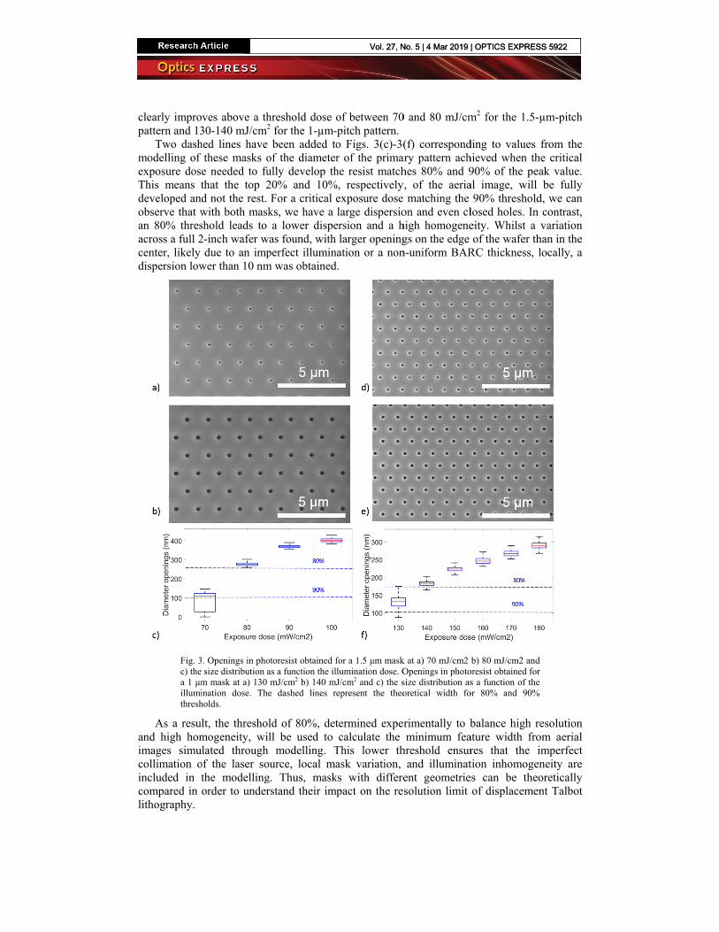
clearly impropattern and 13
Two dashmodelling of exposure doseThis means tdeveloped andobserve that wan 80% thresacross a full 2center, likely dispersion low
Fig. 3c) the a 1 μmillumithresh
As a resuland high homimages simucollimation oincluded in tcompared in lithography.
ves above a th30-140 mJ/cm2
hed lines have these masks oe needed to futhat the top 2d not the rest. with both maskshold leads to 2-inch wafer w
due to an impwer than 10 nm
. Openings in phosize distribution a
m mask at a) 130 ination dose. Theholds.
lt, the thresholmogeneity, willated through
of the laser sothe modellingorder to under
hreshold dose o2 for the 1-µm-been added to
of the diameterully develop th20% and 10%For a critical e
ks, we have a a lower dispeas found, with
perfect illuminm was obtained
otoresist obtained fas a function the ilmJ/cm2 b) 140 mJ
e dashed lines r
ld of 80%, detll be used to
modelling. Tource, local mag. Thus, maskrstand their im
of between 70-pitch pattern.o Figs. 3(c)-3(r of the primahe resist match
%, respectivelyexposure dose large dispersio
ersion and a hlarger opening
nation or a nond.
for a 1.5 μm masklumination dose. OJ/cm2 and c) the sepresent the theo
termined expercalculate the
This lower thask variation,
ks with differempact on the re
0 and 80 mJ/cm
(f) correspondary pattern achhes 80% and 9y, of the aeria matching the on and even clhigh homogenegs on the edge n-uniform BAR
k at a) 70 mJ/cm2 Openings in photosize distribution asoretical width fo
rimentally to bminimum fea
hreshold ensurand illuminat
ent geometriesolution limit
m2 for the 1.5-
ding to values hieved when th90% of the peal image, will
90% thresholdlosed holes. Ineity. Whilst a of the wafer th
RC thickness,
b) 80 mJ/cm2 andoresist obtained fors a function of the
or 80% and 90%
balance high rature width frores that the ition inhomogees can be theof displaceme
-µm-pitch
from the he critical eak value.
be fully d, we can
n contrast, variation
han in the locally, a
d r e
%
resolution om aerial imperfect
eneity are oretically
ent Talbot
Vol. 27, No. 5 | 4 Mar 2019 | OPTICS EXPRESS 5922 Vol. 27, No. 5 | 4 Mar 2019 | OPTICS EXPRESS 5922

3. Impact of mask design on figures of merit
Using the computer model that has been developed, the influence of different parameters on the resolution has been analysed. Amplitude and phase masks have both been modelled for a range of pitches and mask feature sizes. Whilst amplitude masks are commonly used due to their cost and ease of manufacture, phase masks can improve the resolution of classical lithography. Therefore, it is important to understand whether the same is borne out for DTL.
3.1 Amplitude mask
Simulations of the aerial images were generated for mask pitches between 0.5 and 3.2 µm and mask opening diameters from 20 nm to 90% of the pitch with a resolution step of 20 nm in order to allow a good understanding of the impact of the different parameters on the aerial image. The integration was performed over four Talbot lengths to prevent artefacts arising from the grid definition. From the aerial images, the theoretical width, the relative background of intensity and the maximum of the secondary patterns were determined and these have been plotted in Figs. 4(a)-4(c), respectively, as a function of the pitch and feature diameter of the mask.
Figure 4(a) shows that the smallest features are obtained when the mask openings are smaller than the wavelength. With these feature sizes, the diffraction can be considered to arise from an array of point sources with hemispherical wavefronts. However, the transmission is highly reduced for subwavelength holes, where the transmission ( )T λ scales
according to ( ) ( )4: /T dλ λ [21-23]. A second valley giving small features also appears for a
filling factor of 50% though the theoretical width achievable is not quite as small. Sharp vertical and horizontal lines are also apparent along this valley where the minimum feature size abruptly decreases with increasing size. These appear periodically at multiples of the laser wavelength as a result of the incremental addition of further diffraction orders as the wavelength is increased.
The plot of the relative intensity of the background in Fig. 4(b) shows that the background is lower for smaller mask openings. Thus, the highest resolution features can simultaneously be achieved with having a low background.
In contrast to the previous two figures of merit, the plot of the relative intensity of maximum of secondary patterns (Fig. 4(c)) is not as simple. Low maxima of the secondary patterns (dark blue regions in Fig. 4(c) can be obtained in two cases: for small mask openings and particular pitches, or for masks with a filling factor of 33%. This specific value can be explained by diffraction theory. Indeed, in the case of gratings, the disappearance of some diffraction orders can occur if the ratio of the grating width on the period is a rational fraction. The same phenomenon is appearing here with a 2D mask. By tuning the diameter opening, some diffraction orders can be canceled, and so reduce the importance of the secondary pattern. Furthermore, for small mask openings, all the diffraction orders are represented and more or less have the same amplitude. This can explain why the resolution is improved in Fig. 4(a).
Vol. 27, No. 5 | 4 Mar 2019 | OPTICS EXPRESS 5923 Vol. 27, No. 5 | 4 Mar 2019 | OPTICS EXPRESS 5923

Fig. 4and c)
The periodFigs. 4(a)-4(cresolution wireaching a plathe pitch. DTL
Figure 5(b(around 45%)can be decrewavelength (0
Fig. 5of sec
3.2 Phase m
Correspondinrange of pitchin Fig. 6. Thehigher backgbackground isof the secondmaximum.
4. Theoretical a) w) relative intensity
dic nature of tc) as shown inill be obtainedateau. In this aL resolution is b) illustrates t). However, byeased. Further0.75 µm), the s
5. a) Theoretical dicondary patterns as
mask
ng calculations h and feature sie most significaground level. Gs essential for a
dary pattern we
width of the patterof maximum of se
the plots can bn Fig. 5 for ad when the pirea, an improvnot only depen
that at large py choosing a pirmore, when tsecondary patte
iameter of the pats a function of pitc
of the aerial izes, from whicant difference Given that a a good processere only extrac
rn achievable, b) recondary patterns
e seen in crossa fixed openinitch is small.
vement of 100 ndent on the hoitches we havitch of 1.25 or the mask pitcern peak intens
tern achievable anch for a mask open
image were mch the figures obetween the phlarge differencs, the results focted when the b
relative intensity ofor hexagonal amp
s-sections throng of 400 nm.
The resolutionm can be maole opening siz
ve a high seco2 μm, the seco
ch is below bsity drops signi
nd b) relative intenning of 400 nm.
made for a phaof merit were hase and amplce between thor the theoreticbackground wa
of the backgroundmplitude mask.
ough the colou. In Fig. 5(a),
on then decreaade by slightly ze but also on tondary pattern ondary patternbut close to tificantly.
nsity of maximum
ase mask with extracted and dlitude mask is he peak valuecal width and mas less than 70
d
ur plots of the best
ases until changing the pitch. intensity
n intensity twice the
m
a similar displayed the much
e and the maximum 0% of the
Vol. 27, No. 5 | 4 Mar 2019 | OPTICS EXPRESS 5924 Vol. 27, No. 5 | 4 Mar 2019 | OPTICS EXPRESS 5924

The modeamplitude mathe vertical analso present.
Optimisinappears in theto pitch of 6explained bypredominant, Similar to thethe secondaryrespective valin the relative
However, the resolution
Fig. 6and c)
4. Discussio
In this study, wavelength sofeature sizes smaller than tnm will imprdeveloper wit
Various ametal layer onshape of the sthe results forthe rounding the optimum d
Neverthel[9–11]. In ad
elling shows thasks. Indeed, land horizontal p
g all the figure relative inten6% (Fig. 6(b)
y the ratio bethe destructiv
e case of the amy maxima for alleys are not pee intensities of b
these regions n is compromis
6. Theoretical a) w) relative intensity
on
computer simource of 375 nare predicted
the laser wavelrove the resoluth higher contraassumptions han the mask, thstructures havinr very small maof the resist pdevelopment tiess, the modell
ddition, our pre
hat the conditioarger openings periodic featur
res of merit ssity of the back), correspondi
etween the twve interferencesmplitude mask, filling factor oerfectly matchboth the backgdo not coincided.
width of the patterof maximum of se
mulations of thenm and assumito be around
length. It is expution to the sast will permit
ave been madee dark erosionng been omitteask openings a
profile. In partiime to one thatling results agrevious work h
ons to enhance lead to a bette
res previously
imultaneously kground for a ing to a filling
wo phases of s occurring in , there is also aof 33% (Fig. 6ed, their broad
ground and the de consistently
rn achievable, b) recondary patterns
e DTL aerial iing a specific 75-100 nm fo
pected that furtsub 50 nm ran
smaller feature in the modeln of the resist, ed. The finite thand the simplificular, the effet balances highree with other has successfull
the resolution er resolution (Fobserved for t
is not possibconstant ratio g factor of 40the mask. Inthe backgroun
a minimum in (c)). Whilst the
dness allows a secondary mawith high-reso
relative intensity ofor a hexagonal ph
image have bephotoresist an
or an amplitudther decreasingnge. Furthermores to be obtainlling, with thethe flow of thehickness couldfied resist modect of dark eroh contrast with modelling studly validated th
are not the samFig. 6(a)). Nevthe amplitude
ble. A dark bluof feature size
0%. This vallendeed, if one nd won’t be othe relative inte positions of tsimultaneous r
axima. olution feature
of the backgroundhase mask.
een analysed fond developer. Mde mask with g the wavelengore, using a r
ned. e finite thicknee developer an
d impact the acdel would undeosion is likely t
low dark erosidies of the Talbhe model and
me as for vertheless,
mask are
ue valley diameter
ey can be phase is ptimized. tensity of these two reduction
s. And so
d
for a laser Minimum openings
gth to 193 resist and
ess of the nd the 3D curacy of
erestimate to reduce ion. bot effect predicted
Vol. 27, No. 5 | 4 Mar 2019 | OPTICS EXPRESS 5925 Vol. 27, No. 5 | 4 Mar 2019 | OPTICS EXPRESS 5925
experimental results qualitatively; for high illumination doses for certain hexagonal masks, the secondary patterns were seen to merge to create ring structures after development. The shape of the ring obtained experimentally was found to correspond well with the modelled shape [15] and could be used to create resonant cavity modes in axial InGaN/GaN nanotube microcavities.
One of the benefits of DTL is being able to vary the exposure dose to create a large range of feature diameters; a phenomenon that arises from the shape of the intensity peaks in the aerial image. For example, the 1.5 μm hexagonal amplitude mask with 800 nm openings allows a range of features in resist from 250 - 650 nm; thus demonstrating the flexibility of DTL. For this purpose having a low background and a less pronounced secondary pattern are more important factors than the resolution and these are better satisfied with phase masks.
By comparing Figs. 4-6, it can be seen that for mask pitches smaller than two wavelengths, both phase and amplitude masks achieve the same resolution. In this case, a phase mask would be preferred because of the higher transmission through the mask, leading to a shorter illumination time. For higher pitches, an amplitude mask would offer the smallest features, but at the expense of a long exposure time.
5. Conclusion
Displacement Talbot Lithography is a new lithography method that can pattern periodic features across a large area quickly and cheaply. The conditions to reach the smallest features with DTL are not trivial and in certain situations conflict with the optimisation of other figures of merit that influence the lithography process. For a specific i-line resist, the impact of the pitch and the size of the openings on the mask has been found and analysed not only on the minimum size feature achievable, but also the sensitivity of the resolution, the background, and the unwanted secondary pattern intensities. This study shows how sub-100 nm features can be achieved with DTL across large areas with conventional i-line resists and illumination. This limit is substantially below other classical photolithography methods using the same illumination wavelength.
6. Appendices
6.1 Experimental data
Silicon wafers were coated with a bottom antireflective layer (Wide 30, Brewer Science) prior to a 240 nm positive resist (Ultra i-123 diluted from 800 nm as supplied). The wafers were exposed via DTL using a hexagonal amplitude mask with either a 1.5 μm pitch and 800 nm mask openings or with a 1 μm pitch and 550 nm openings. The Talbot length associated with these masks are 8.80 μm and 3.80 μm, respectively (the section 6.2). A Gaussian velocity integration was applied and a travel distance of 8 Talbot lengths was chosen to ensure homogenous integration over several Talbot motifs. Multiple series of illuminations were realized to ensure a high reproducibility of the process: 70 to 100 mJ/cm2 for 1.5 μm, and 130 to 180 mJ/cm2 for 1 μm, with 10 mJ/cm2 step. The wafers were immersed for 210 s in the developer (MF CD26). This development time was chosen to reach a 10% contrast in the resist profile calculated thanks to the Dills model [24–26].
The statistical data on the feature diameters in Fig. 3 was determined from image analysis of 3 SEM pictures per sample. The pictures were consistently taken around the center of the wafer and the magnification was chosen to observe around a hundred features in one picture.
6.2 Hexagonal mask modeling
The non-primitive unit cell size for a hexagonal organization has a specific characteristic: one
cell edge is 3 larger than the other. Due to this being an irrational number and the use of matrices in MATLAB, a rounding error will occur during the definition of the matrix size. This error can be mitigated by increasing the resolution without sacrificing the computational
Vol. 27, No. 5 | 4 Mar 2019 | OPTICS EXPRESS 5926 Vol. 27, No. 5 | 4 Mar 2019 | OPTICS EXPRESS 5926

time. Furtherm
not the nearesSo the Tal
6.3 Square m
The use of sq
smaller pitch.the mask (Fig8(b), the maxopenings are between the tw
6.3.1 Amplitu
The conclusiamplitude maintensity of ththan for the hand pitches n
of the second(around 530 nand since the in the modellchosen for spsecondary pat
more, for hexa
st neighbour dilbot length calc
mask
quare mask wi
. The distance g. 7). However,xima aligned not exactly th
wo patterns is
Fig. 7. Reductio
ude mask
ons with the ask; small mahe backgroundexagonal maskot matching th
dary patterns nm). Figure 8(dintegration wa
ling. In conclupecific pitchesttern is unavoid
agonal masks, t
stance but thisculation becom
TL =
ith DTL allow
between the p, the intensity owith the holes
he same. As a important for h
on of pitch for a 1
square amplitask openings d is low. Howek. A valley withe optimum va
will be low fd) shows that aas realized oveusion, to obtais, e.g. 1.05, 2 dable.
the distance us
distance multimes:
2
2
.41 1
.3p
λλ
=
− −
ws the creation
pattern in the rof alternate mas and the addresult, the an
homogenous pa
μm square array. a
tude mask areresult in sma
ever, the seconth low values ealues for the tw
for pitches sma difference ofer 4 Talbot lenin a good hom
or 2.5 μm. N
sed in the Talb
iplied by 3 /
of a new squ
resist will be axima in the paditional maximnalysis of the datterning and u
a) Mask and b) aer
e similar to thaller resist feandary pattern iexists, but it ocwo previous pa
maller than 2f 6% can appeangths, this is unmogeneity, smNevertheless, a
bot period calc
2 [27].
are organisatio
2 smaller thaattern can diffe
ma created betwdifference of auniformity.
rial image.
hose of the hatures and theintensity is eveccurs for mask arameters. The
times the waar between thenlikely to be anall openings sa high intensi
ulation is
on with a
an that on er; in Fig. ween the amplitude
hexagonal e relative en higher openings intensity
avelength e patterns, n artefact should be ity of the
Vol. 27, No. 5 | 4 Mar 2019 | OPTICS EXPRESS 5927 Vol. 27, No. 5 | 4 Mar 2019 | OPTICS EXPRESS 5927

Fig. 8relativbetwe
6.3.2 Phase
The same conphase mask. Lin this area, hexagonal one
Fig. 9relativpatter
. Theoretical a) wive intensity of meen neighbouring f
mask
nclusions can Larger openingand the valuee.
9. Theoretical a) wive intensity of mns.
idth of the pattern maximum of seconfeatures as a functi
be drawn whegs will give a he of the secon
idth of the pattern maximum of seco
achievable, b) relandary patterns anion of the pitch and
en using a squhigher resolutiondary maxima
achievable, b) relaondary patterns a
ative intensity of tnd d) Ratio of md the hole diamete
uare phase mason. The backgris going to b
ative intensity of tand d) Ratio betw
the background, c)maximum intensityer.
sk as for the hround will be
be smaller than
the background, c)ween neighboring
) y
hexagonal quite low n for the
) g
Vol. 27, No. 5 | 4 Mar 2019 | OPTICS EXPRESS 5928 Vol. 27, No. 5 | 4 Mar 2019 | OPTICS EXPRESS 5928

In Fig. 9(d) the intensity ratio between neighbouring patterns shows similar values to the amplitude mask with some parts being almost the same. In order to follow a valley corresponding to a specific filling factor to obtain a good resolution, specific pitches and opening diameters should be targeted.
6.3.3 Discussion
For square mask, the smallest feature will be obtained with the amplitude mask but the secondary pattern intensity is significant and could even be critical. In square phase mask, for large openings, the secondary patterns are not going to as high as the hexagonal case, with reasonably small features being achievable. So for the patterning of square array, a phase mask will be a better choice for a high resolution with limited parasitic effect.
Funding
Engineering & Physical Science Research Council, UK (EPSRC) (EP/M015181/1, EP/M022862/1)
Acknowledgments
All data created during this research is openly available from the University of Bath Research Data Archive at [https://doi.org/10.15125/BATH-00570].
References
1. J. J. Baumberg, T. A. Kelf, Y. Sugawara, S. Cintra, M. E. Abdelsalam, P. N. Bartlett, and A. E. Russell, “Angle-Resolved Surface-Enhanced Raman Scattering on Metallic Nanostructured Plasmonic Crystals,” Nano Lett. 5(11), 2262–2267 (2005).
2. W. Fan, S. Zhang, K. J. Malloy, and S. R. J. Brueck, “Large-area, infrared nanophotonic materials fabricated using interferometric lithography,” J. Vac. Sci. Technol. 23(6), 2700–2704 (2005).
3. E. D. Le Boulbar, P. J. P. Chausse, S. Lis, and P. A. Shields, “Displacement Talbot lithography: an alternative technique to fabricate nanostructured metamaterials,” Proc. SPIE 10248, 254–256 (2017).
4. C. Wagner and N. Harned, “Lithography gets extreme,” Nat. Photonics 4(1), 24–26 (2010). 5. G. Tallents, E. Wagenaars, and G. Pert, “Lithography at EUV wavelengths,” Nat. Photonics 4(12), 809–811
(2010). 6. C. Vieu, F. Carcenac, A. Pépin, Y. Chen, M. Mejias, A. Lebib, L. Manin-Ferlazzo, L. Couraud, and H. Launois,
“Electron beam lithography: resolution limits and applications,” Appl. Surf. Sci. 164(1–4), 111–117 (2000). 7. M. C. Traub, W. Longsine, and V. N. Truskett, “Advances in Nanoimprint Lithography,” Annu. Rev. Chem.
Biomol. Eng. 7(1), 583–604 (2016). 8. S. Fujita, S. Maruno, H. Watanabe, Y. Kusumi, and M. Ichikawa, “Periodical nanostructure fabrication using
electron interference fringes produced by scanning interference electron microscope,” Appl. Phys. Lett. 66(20), 2754–2756 (1995).
9. C. Lu and R. H. Lipson, “Interference lithography: a powerful tool for fabricating periodic structures,” Laser Photonics Rev. 4(4), 568–580 (2010).
10. H. H. Solak, C. Dais, and F. Clube, “Displacement Talbot lithography: a new method for high-resolution patterning of large areas,” Opt. Express 19(11), 10686–10691 (2011).
11. A. Isoyan, F. Jiang, Y. C. Cheng, F. Cerrina, P. Wachulak, L. Urbanski, J. Rocca, C. Menoni, and M. Marconi, “Talbot lithography: Self-imaging of complex structures,” J. Vac. Sci. Technol. 27(6), 2931–2937 (2009).
12. H. H. Solak, C. Dais, F. Clube, and L. Wang, “Phase shifting masks in Displacement Talbot Lithography for printing nano-grids and periodic motifs,” Microelectron. Eng. 143, 74–80 (2015).
13. L. Wang, F. Clube, C. Dais, H. H. Solak, and J. Gobrecht, “Sub-wavelength printing in the deep ultra-violet region using Displacement Talbot Lithography,” Microelectron. Eng. 161, 104–108 (2016).
14. P. M. Coulon, G. Kusch, E. D. Le Boulbar, P. Chausse, C. Bryce, R. W. Martin, and P. A. Shields, “Hybrid top-down/bottom-up fabrication of regular arrays of AlN nanorods for deep-UV core-Shell LEDs,” Phys. Status Solidi, 1700445 (2017).
15. P. M. Coulon, J. R. Pugh, M. Athanasiou, G. Kusch, E. D. Le Boulbar, A. Sarua, R. Smith, R. W. Martin, T. Wang, M. Cryan, D. W. E. Allsopp, and P. A. Shields, “Optical properties and resonant cavity modes in axial InGaN/GaN nanotube microcavities,” Opt. Express 25(23), 28246–28257 (2017).
16. S. Xie, B. Schurink, E. J. W. Berenschot, R. M. Tiggelaar, H. J. G. E. Gardeniers, and R. Luttge, “Displacement Talbot lithography nanopatterned microsieve array for directional neuronal network formation in brain-on-chip,” J. Vac. Sci. Technol. B 34(6), 06KI02 (2016).
17. C. S. Lee, Y. Y. Lee, K. S. L. Chong, L. Wang, C. Dais, F. Clube, H. H. Solak, I. Mohacsi, C. David, and R. Bischofberger, “High-resolution, high-aspect-ratio iridium-nickel composite nanoimprint molds,” Journal of Vacuum Science 34(6), 061804 (2016).
Vol. 27, No. 5 | 4 Mar 2019 | OPTICS EXPRESS 5929 Vol. 27, No. 5 | 4 Mar 2019 | OPTICS EXPRESS 5929

18. H. Le-The, E. Berenschot, R. M. Tiggelaar, N. R. Tas, A. van den Berg, and J. C. T. Eijkel, “Shrinkage Control of Photoresist for Large-Area Fabrication of Sub-30 nm Periodic Nanocolumns,” Advance Mater Technology 2(3), 1600238 (2017).
19. L. Wang, F. Clube, C. Dais, H. H. Solak, and J. Gobrecht, “Sub-wavelength printing in the deep ultra-violet region using Displacement Talbot Lithography,” Microelectron. Eng. 161, 104–108 (2016).
20. J. Maaß, O. Sandfuchs, D. Thomae, A. Gatoo and R. Brunner, “Effective and flexible modeling approach to investigate various 3D Talbot carpets from a spatial finite mask”, Journal of the European Optical Society 8 (2013).
21. C. Genet and T. W. Ebbesen, “Light in tiny holes,” Nature 445(7123), 39–46 (2007). 22. T. Ishi, J. Fujikata and K. Ohashi, “Large Optical transmission through a Single Subwavelength Hole Associated
with a Sharp-Apex Grating”44(1L), 170–172 (2005). 23. L. Salomon, F. Grillot, A. V. Zayats, and F. de Fornel, “Near-Field Distribution of Optical Transmission of
Periodic Subwavelength Holes in a Metal Film,” Phys. Rev. Lett. 86(6), 1110–1113 (2001). 24. F. H. Dill, W. P. Hornberger, P. S. Hauge, and J. M. Shaw, “Characterization of positive photoresist,”
Transaction on electron devices 22(7), 445–452 (1975). 25. G. Arthur, C. A. Mack, and B. Martin, “A new development model for lithography simulation,”. Olin
Microlithography Seminar 97(4), 55–56 (1997). 26. C. Mack, Fundamental Principles of Optical Lithography (Wiley, 2012). 27. C. S. Guo, X. Yin, L.-W. Zhu, and Z.-P. Hong, “Analytical expression for phase distribution of a hexagonal
array at fractional Talbot planes,” Opt. Lett. 32(15), 2079–2081 (2007).
Vol. 27, No. 5 | 4 Mar 2019 | OPTICS EXPRESS 5930 Vol. 27, No. 5 | 4 Mar 2019 | OPTICS EXPRESS 5930