University of Alberta Library Release Form Name of Author
198
University of Alberta Library Release Form Name of Author: Matthew Reid Title of Thesis: Terahertz radiation from InAs, GaAs and InP emitters at high excitation fluences and applications Degree: Doctor of Philosophy Year this Degree Granted: 2005 Permission is hereby granted to the University of Alberta Library to reproduce single copies of this thesis and to lend or sell such copies for private, scholarly or scientific research purposes only. The author reserves all other publication and other rights in association with the copy- right in the thesis, and except as hereinbefore provided, neither the thesis nor any substantial portion thereof may be printed or otherwise reproduced in any material form whatever without the author’s prior written permission. . . . . . . . . . . . . . . . . . . . Matthew Reid University of Alberta, ECERF 2nd floor Edmonton, Alberta Canada, T6G 2J1 Date: . . . . . . . . .
Transcript of University of Alberta Library Release Form Name of Author

University of Alberta
Library Release Form
Name of Author: Matthew Reid
Title of Thesis: Terahertz radiation from InAs, GaAs and InP emitters at high excitation
fluences and applications
Degree: Doctor of Philosophy
Year this Degree Granted: 2005
Permission is hereby granted to the University of Alberta Library to reproduce single
copies of this thesis and to lend or sell such copies for private, scholarly or scientific
research purposes only.
The author reserves all other publication and other rights in association with the copy-
right in the thesis, and except as hereinbefore provided, neither the thesis nor any
substantial portion thereof may be printed or otherwise reproduced in any material form
whatever without the author’s prior written permission.
. . . . . . . . . . . . . . . . . . .
Matthew Reid
University of Alberta, ECERF 2nd floor
Edmonton, Alberta
Canada, T6G 2J1
Date: . . . . . . . . .

Dr. Seuss Knows Graduate School
You have brains in your head.You have feet in your shoes.You can steer yourselfin any direction you choose.You’re on your own. And you know what you know.And YOU are the guy who’ll decide where to go.
Out there things can happenand frequently doto people as brainyand footsy as you.
I’m sorry to say sobut, sadly, it’s truethat bang-ups and hang-upscan happen to you.
And when you’re in a slump,you’re not in for much fun.Un-slumping yourselfis not easily done.
You’ll get mixed up, of course,as you already know.You’ll get mixed upwith many strange birds as you go.So be sure when you step.Step with care and great tactand remember that life’sa great balancing act.Just never forget to be dextrous and deft.And never mix up your right foot with your left.
And will you succeed?Yes! You will, indeed!(98 and 3/4 percent guaranteed ).
– Dr. Seuss(1904 - 1991)Oh the Places You’ll Go!

University of Alberta
Terahertz radiation from InAs, GaAs and InP emitters at high
excitation fluences and applications
by
Matthew Reid
A thesis submitted to the Faculty of Graduate Studies and Research in partial fulfillment
of the requirements for the degree of Doctor of Philosophy.
Department of Electrical and Computer Engineering
Edmonton, Alberta
Fall 2005

University of Alberta
Faculty of Graduate Studies and Research
The undersigned certify that they have read, and recommend to the Faculty of Graduate
Studies and Research for acceptance, a thesis entitled Terahertz radiation from InAs,
GaAs and InP emitters at high excitation fluences and applications submitted by
Matthew Reid in partial fulfillment of the requirements for the degree of Doctor of
Philosophy.
. . . . . . . . . . . . . . . . . . .
Robert Fedosejevs
. . . . . . . . . . . . . . . . . . .
Tony F. Heinz
. . . . . . . . . . . . . . . . . . .
Ying Y. Tsui
. . . . . . . . . . . . . . . . . . .
Clarence Capjack
. . . . . . . . . . . . . . . . . . .
David Routledge
. . . . . . . . . . . . . . . . . . .
Frank Hegmann
Date: . . . . . . . . .

To my family: Victoria and Dean - the only reason I have maintained my sanity
throughout, and the support of my loving wife Christina.

Abstract
In this thesis, terahertz emission from semiconductor surfaces is studied at high optical
excitation fluences in order to investigate the scaling of such sources to high efficiencies.
A quantitative comparison of terahertz emission from InAs surfaces, one of the more
efficient semiconductor sources, to the most efficient reported pulsed terahertz emitter, a
large-aperture GaAs photoconductive switch, is carried out. It is found that at high bias
voltages the large-aperture photoconductive switch is more efficient at converting optical
to far-infrared energy but that the InAs semiconductor source has a higher frequency
bandwidth.
In the high excitation fluence regime, it is found that the dominant emission mech-
anism from InAs surfaces changes from the previously reported photo-carrier dominated
processes at low excitation fluences. A detailed calculation of bulk and surface electric-
field induced optical rectification from zinc blende crystals is performed. The calculations
are compared to the experimental observation of optical second-harmonic generation and
terahertz emission from InAs surfaces for various crystal orientations. The results indi-
cate that the dominant emission mechanism for terahertz radiation from InAs is surface
electric-field induced optical rectification.
A comparison of emission of THz radiation from porous crystalline surfaces of InP
versus unstructured surfaces was carried out. It was demonstrated, for the first time,
that an increased conversion efficiency of terahertz radiation could be achieved with
the introduction of porosity and in particular that the optical rectification component

of terahertz emission from InP surfaces could be enhanced with the introduction of
porosity. The mechanism for the enhancement is tentatively attributed to local-field
enhancement within the porous network.
A terahertz time-domain spectrometer set-up was constructed, employing a semi-
large aperture photoconductive switch. This system was characterized and applied to the
study of wood and wood products. Specifically, it was demonstrated in a transmission
mode that wood samples exhibit both birefringence and diattenuation. These results
could lead to potential applications for the determination of fiber orientation in wood
products such as the analysis of fiber orientation in paper products.

Acknowledgments
I would like to express my gratitude for the access to expert knowledge and guidance
as well as the many opportunities for career advancement that have been provided by
my supervisor, Dr. Fedosejevs. I would also like to acknowledge significant support from
Dr. Y. Y. Tsui and Dr.Hegmann with some of the finer details of this thesis work.
This project would not have been possible without the expertise provided by Blair
Harwood and Rick Conrad with many of the electronics and technological details.
My peers provided me with the support required to reach my goals, as well as
much valuable input along the way. For this, I sincerely express my gratitude to Sean
Kirkwood, Mike Taschuk, Michael Argument, James Gospodyn, Roman Holenstein and
Craig Unick. I am also very grateful to these same people for providing me with the
opportunity to learn the game of bridge.
Of all the things I have accomplished during the course of my degree, I am most
grateful for being blessed with two wonderful children, Victoria and Dean, and a won-
derful wife, Christina. I would also like to thank my friends and family for supporting
me in times of need. I would like to thank my mother, Debbie Reid, and brother, Mark
Reid for their support along the way. I would also like to thank my grandparents, Ed
and Jean Boutilier, for their support. I am very grateful to my wonderful in-laws, Eva
and John Werlberger, for helping with our children and making it possible to pursue our
family goals. I would also like to thank Mark Shegelski for keeping me on-track and
focused, as well as Val Hart, Dave Reid and Luke Reid for their help along the way.

I would also like to acknowledge the financial support provided by NSERC, iCORE
and MPB Technologies Inc., without which I would not have been able to do this work.

Contents
1 Introduction 1
1.1 Context of terahertz radiation in this thesis . . . . . . . . . . . . . . . 1
1.2 Applications . . . . . . . . . . . . . . . . . . . . . . . . . . . . . . . . 2
1.3 Generation of terahertz radiation . . . . . . . . . . . . . . . . . . . . . 3
1.3.1 Photo-carrier related emission mechanisms . . . . . . . . . . . . 4
1.3.2 Bulk optical rectification . . . . . . . . . . . . . . . . . . . . . 6
1.3.3 Surface electric-field induced optical rectification . . . . . . . . 8
1.4 Thesis statement . . . . . . . . . . . . . . . . . . . . . . . . . . . . . 10
1.5 Layout of the thesis . . . . . . . . . . . . . . . . . . . . . . . . . . . . 10
2 Description of the experimental set-up used for the generation and de-
tection of THz radiation 12
2.1 General description and overview . . . . . . . . . . . . . . . . . . . . . 12
2.2 Electronic and Electro-optic Components . . . . . . . . . . . . . . . . . 14
2.3 Optics . . . . . . . . . . . . . . . . . . . . . . . . . . . . . . . . . . . 15

2.4 Terahertz detector . . . . . . . . . . . . . . . . . . . . . . . . . . . . . 15
2.5 Terahertz emitters . . . . . . . . . . . . . . . . . . . . . . . . . . . . . 16
3 Electro-optic detection of terahertz radiation 17
3.1 Detection of pulsed terahertz radiation . . . . . . . . . . . . . . . . . . 17
3.1.1 Background . . . . . . . . . . . . . . . . . . . . . . . . . . . . 17
3.1.2 Thermal detection . . . . . . . . . . . . . . . . . . . . . . . . . 18
3.1.3 photoconductive switch and electro-optic sampling . . . . . . . 19
3.2 Calculation of electro-optic response in ZnTe . . . . . . . . . . . . . . 22
3.2.1 Balanced detection . . . . . . . . . . . . . . . . . . . . . . . . 22
3.2.2 Induced birefringence . . . . . . . . . . . . . . . . . . . . . . . 28
3.2.3 Polarization dependence of ZnTe electro-optic detection . . . . 33
3.2.4 ZnTe electro-optic detection as a polarization analyzer . . . . . 34
3.3 Examination of the ZnTe electro-optic response . . . . . . . . . . . . . 38
3.3.1 Calibration of the electro-optic response of lithium niobate . . . 38
3.3.2 Comparison of ZnTe and LiNbO3 electro-optic responses . . . . 42
4 Comparison of large-aperture photoconductive switch and InAs surface
emission 46
4.1 Description of the large-aperture photoconductive switch . . . . . . . . 46
4.2 Direct comparison . . . . . . . . . . . . . . . . . . . . . . . . . . . . . 48
5 Terahertz radiation from InAs surfaces at high excitation fluences 59

5.1 Emission mechanism of terahertz radiation from InAs (100) . . . . . . . 60
5.2 Bulk electric-dipole radiation . . . . . . . . . . . . . . . . . . . . . . . 65
5.2.1 Calculation of bulk electric-dipole radiation . . . . . . . . . . . 65
5.2.2 Measurements of optical second-harmonic generation from InAs 72
5.3 Electric-field induced nonlinearity . . . . . . . . . . . . . . . . . . . . . 76
5.3.1 Calculation of surface electric-field induced optical rectification . 76
5.3.2 Terahertz emission from InAs . . . . . . . . . . . . . . . . . . . 79
5.4 Comparison of second-harmonic generation and terahertz emission from
InAs . . . . . . . . . . . . . . . . . . . . . . . . . . . . . . . . . . . . 87
6 Terahertz emission from porous and unstructured InP 92
6.1 InP (111) . . . . . . . . . . . . . . . . . . . . . . . . . . . . . . . . . 93
6.1.1 Experimental . . . . . . . . . . . . . . . . . . . . . . . . . . . 93
6.2 InP (100) . . . . . . . . . . . . . . . . . . . . . . . . . . . . . . . . . 100
7 Semi-large aperture photoconductive switch 109
7.1 Description of the SLAPCS . . . . . . . . . . . . . . . . . . . . . . . . 109
7.2 Construction of the SLAPCS . . . . . . . . . . . . . . . . . . . . . . . 111
7.3 Performance of the SLAPCS . . . . . . . . . . . . . . . . . . . . . . . 111
7.3.1 Terahertz emission scaling with applied bias field . . . . . . . . 112
7.3.2 Terahertz emission scaling with optical pump energy . . . . . . 113
7.3.3 Noise scaling with operation frequency . . . . . . . . . . . . . . 114

7.3.4 Estimate of source efficiency . . . . . . . . . . . . . . . . . . . 116
8 Applications 124
8.1 Birefringence of wood . . . . . . . . . . . . . . . . . . . . . . . . . . . 124
8.2 Waveplates constructed from solid wood . . . . . . . . . . . . . . . . . 128
8.3 Birefringence of lens paper . . . . . . . . . . . . . . . . . . . . . . . . 131
8.4 A method to image wood in transmission . . . . . . . . . . . . . . . . 133
9 Conclusion and future work 150
9.1 Conclusions . . . . . . . . . . . . . . . . . . . . . . . . . . . . . . . . 150
9.2 Future Work . . . . . . . . . . . . . . . . . . . . . . . . . . . . . . . . 151
Bibliography 153
A Appendix 164
A.1 Electro-optic detection in ZnTe . . . . . . . . . . . . . . . . . . . . . . 164
A.1.1 Derivation of relation 3.26 . . . . . . . . . . . . . . . . . . . . 164
A.1.2 Derivation of Eq. 3.35 . . . . . . . . . . . . . . . . . . . . . . 165
A.2 Calculation of the bulk electric-dipole contribution to nonlinear suscep-
tibility . . . . . . . . . . . . . . . . . . . . . . . . . . . . . . . . . . . 166
A.3 Calculation of surface electric-field induced nonlinearity . . . . . . . . . 168

List of Figures
1.1 Schematic diagram of THz emission from photo-carrier effects. . . . . . 5
1.2 Schematic diagram of THz emission from bulk optical rectification. . . 7
1.3 Schematic diagram of THz emission from surface electric-field induced
opticalrectification. . . . . . . . . . . . . . . . . . . . . . . . . . . . . 9
2.1 Schematic diagram of general THz set-up. . . . . . . . . . . . . . . . . 13
3.1 Photo-conductive vs. electro-optic detection of THz radiation. . . . . . 20
3.2 Probe and THz polarization geometry in ZnTe calculation. . . . . . . . 23
3.3 Induced birefringent axes geometry in ZnTe calculation. . . . . . . . . . 24
3.4 Schematic diagram of balanced detection for ZnTe electro-optic detection. 25
3.5 Birefringent axes and THz polarization for ZnTe calculation. . . . . . . 29
3.6 Orientation of the induced birefringent axes in ZnTe. . . . . . . . . . . 32
3.7 Polarization orientations for ZnTe as a polarization analyzer. . . . . . . 35
3.8 Experimental and theoretical polarization dependencies for ZnTe as a
polarization analyzer. . . . . . . . . . . . . . . . . . . . . . . . . . . . 37

3.9 Experimental set-up for measuring the electro-optic coefficient in LiNbO3. 40
3.10 Phase retardance as a function of applied bias field in LiNbO3. . . . . . 41
3.11 THz waveforms from a large-aperture photoconductive switch measured
in ZnTe and LiNbO3. . . . . . . . . . . . . . . . . . . . . . . . . . . . 43
4.1 Set-up used for comparing InAs and GaAs large-aperture photoconduc-
tive emitters. . . . . . . . . . . . . . . . . . . . . . . . . . . . . . . . . 54
4.2 Saturation measurements for InAs and GaAs. . . . . . . . . . . . . . . 55
4.3 THz waveforms defining pulsewidth in the time domain. . . . . . . . . 56
4.4 Conversion efficiencies measured from GaAs and InAs emitters. . . . . . 57
4.5 Frequency spectra measured for GaAs and InAs emitters. . . . . . . . . 58
5.1 Crystal orientation dependence of THz emission from InAs (100). . . . 62
5.2 Polarization dependence of THz emission from InAs (100). . . . . . . . 63
5.3 Geometry for bulk and surface-field induced optical rectification calcula-
tions. . . . . . . . . . . . . . . . . . . . . . . . . . . . . . . . . . . . . 66
5.4 Pump beam polarization definitions for bulk and surface-field induced
optical rectification calculations. . . . . . . . . . . . . . . . . . . . . . 70
5.5 Set-up for measuring second-harmonic emission from InAs surfaces. . . 73
5.6 Experimental and theoretical curves for SH emission from InAs surfaces. 74
5.7 Set-up for measuring THz emission from InAs surfaces. . . . . . . . . . 81
5.8 Experimental and theoretical curves for THz emission from InAs surfaces. 82

5.9 THz (s-polarized) emission with theoretical curves for (110) InAs. . . . 85
5.10 THz (p-polarized) emission with theoretical curves for (110) InAs. . . . 86
5.11 Experimental and theoretical curves for THz and SH emission from InAs. 88
6.1 SEM micrograph of porous InP (111). . . . . . . . . . . . . . . . . . . 94
6.2 Set-up for measuring THz emission from bulk and porous InP. . . . . . 95
6.3 THz signals from bulk and porous InP (111). . . . . . . . . . . . . . . 96
6.4 Excitation fluence dependence of THz from bulk and porous InP (111). 98
6.5 Crystal orientation dependence of THz from bulk and porous InP (111). 99
6.6 SEM micrograph of porous InP (100). . . . . . . . . . . . . . . . . . . 101
6.7 Crystal orientation dependence of p-polarized THz from bulk and porous
InP (100). . . . . . . . . . . . . . . . . . . . . . . . . . . . . . . . . . 102
6.8 Crystal orientation dependence of p- and s-polarized THz from porous
InP (100). . . . . . . . . . . . . . . . . . . . . . . . . . . . . . . . . . 103
6.9 Crystal orientation dependence of s-polarized THz from bulk and porous
InP (100). . . . . . . . . . . . . . . . . . . . . . . . . . . . . . . . . . 104
6.10 Crystal orientation dependence of p-polarized SH emission from bulk and
porous InP (100). . . . . . . . . . . . . . . . . . . . . . . . . . . . . . 106
6.11 Crystal orientation dependence of s-polarized SH emission from bulk and
porous InP (100). . . . . . . . . . . . . . . . . . . . . . . . . . . . . . 107
7.1 Schematic diagram of the semi-large aperture photoconductive switch. . 112

7.2 Set-up for using the semi-large aperture photoconductive switch. . . . . 113
7.3 Dependence of THz emission from the SLAPCS on applied bias field. . 119
7.4 Dependence of THz emission from the SLAPCS on excitation fluence. . 120
7.5 Noise definition for a typical THz waveform measured from the SLAPCS. 121
7.6 Frequency resolved noise measurements made on the SLAPCS. . . . . . 122
7.7 THz waveform with amplitude in V/cm from the SLAPCS. . . . . . . . 123
8.1 Time-domain birefringence of oak. . . . . . . . . . . . . . . . . . . . . 125
8.2 Frequency resolved index of refraction and absorption measured in the
THz range for oak wood. . . . . . . . . . . . . . . . . . . . . . . . . . 135
8.3 Time domain THz signals measured in transmission through spruce wood.136
8.4 Time-domain birefringence observation in THz transmission through spruce.137
8.5 Frequency resolved index of refraction and absorption measured in the
THz range for spruce wood. . . . . . . . . . . . . . . . . . . . . . . . . 138
8.6 Schematic diagram of the grain orientation in spruce. . . . . . . . . . . 139
8.7 THz polarization characteristics in transmission through spruce at 320
GHz. . . . . . . . . . . . . . . . . . . . . . . . . . . . . . . . . . . . . 140
8.8 THz polarization characteristics in transmission through spruce at 356
GHz. . . . . . . . . . . . . . . . . . . . . . . . . . . . . . . . . . . . . 141
8.9 THz polarization characteristics in transmission through spruce at 391
GHz. . . . . . . . . . . . . . . . . . . . . . . . . . . . . . . . . . . . . 142

8.10 THz polarization characteristics in transmission through spruce at 711
GHz. . . . . . . . . . . . . . . . . . . . . . . . . . . . . . . . . . . . . 143
8.11 Schematic defining the operating point for time-domain birefringence
measurement. . . . . . . . . . . . . . . . . . . . . . . . . . . . . . . . 144
8.12 Time-domain measurement of birefringence of lens paper. . . . . . . . . 145
8.13 Observation of time-delay due to birefringence in lens paper. . . . . . . 146
8.14 Frequency resolved index of refraction measured by THz transmission
through lens paper. . . . . . . . . . . . . . . . . . . . . . . . . . . . . 147
8.15 Optical image of douglas fir. . . . . . . . . . . . . . . . . . . . . . . . 148
8.16 Linear THz transmission map of douglas fir. . . . . . . . . . . . . . . . 148
8.17 Optical and THz image of douglas fir. . . . . . . . . . . . . . . . . . . 149

List of Tables
3.1 Zeros of the polarization response function of the ZnTe electro-optic
detector (Equations 3.37 and 3.38). . . . . . . . . . . . . . . . . . . . 36
3.2 Extrema of the polarization response function of the ZnTe electro-optic
detector (Equations 3.37 and 3.38). . . . . . . . . . . . . . . . . . . . 36
4.1 Parameters used in estimation of optical to far-infrared conversion efficiency 51
5.1 Rotation matrices to bring crystal coordinates to beam coordinate system 67
5.2 Electric dipole susceptibility tensor, χ(2)(φ), in the transformed coordi-
nate systems . . . . . . . . . . . . . . . . . . . . . . . . . . . . . . . . 69
5.3 THz or SH field strengths for different polarization combinations. Com-
binations are listed as Ein,out. . . . . . . . . . . . . . . . . . . . . . . . 72
5.4 Measured and calculated values for ratios of the coefficients in the fitting
functions. The ratios are obtained by using the fitting functions and the
functional dependence of the radiation on the angle φ from Table. 5.3.
Error bars on the measured values are 3 σ errors in this case. . . . . . . 75

5.5 THz field strengths for different polarization combinations. Combina-
tions are listed as Ein,out. . . . . . . . . . . . . . . . . . . . . . . . . . 80
8.1 Table of birefringence measurements. Those listed with a (*) superscript
reflect data that was taken only in the time domain due to poor signal-
to-noise ratios. . . . . . . . . . . . . . . . . . . . . . . . . . . . . . . . 128

Definitions
Symbols
A Area
α Power absorption coefficient
c Speed of light in vacuum
dij Succeptibility tensor element in contracted notation
∂ij Effective second-order susceptibility tensor element
E Electric field
e Electronic charge
ε Dielectric permittivity
F Fluence, Flux
g Conductance
Γ Phase retardance
H(ω) Frequency-dependent transfer function
h Planck’s constant
I Current, Optical intensity
k Imaginary part of the complex index of refraction
L Thickness

λi Eigenvalues
λ Wavelength
Mrot Jones matrix for rotation
MΓ Jones matrix for phase retardance
µ Mobility
no Ordinary index of refraction
ne Extraordinary index of refraction
n Index of refraction
n Complex index of refraction
n(t) Carrier density
ηij Impermeability tensor element
η0 Impedance of free-space
η Conversion efficiency
P Power
P Polarization
φ,Ψ,θ Angle
Q Charge
q Charge
R Power reflectivity

Rij Rotation transformation matrix element
rij Linear electro-optic tensor element
reff Effective linear electro-optic coefficient
σs Surface conductivity
Ti Far-infrared Fresnel transmission coefficient
ti Optical Fresnel transmission coefficient
τR Carrier recombination time
ν Frequency (Hz)
v Velocity
W Energy
Ω Frequency (rad / s)
ω Frequency (rad / s)
χ Susceptibility
Abbreviations, Acronyms
THz Terahertz
LAPCS Large-aperture photoconductive switch
SLAPCS Semi-large aperture photoconductive switch
OR Optical rectification

SH Second Harmonic
SHG Second-harmonic generation
lhs left hand side

Chapter 1
Introduction
The terahertz portion of the electromagnetic spectrum is roughly defined as the fre-quency range from 100 GHz to 10 THz. At 1 THz (single oscillation period of 1 ps),the free-space wavelength of the radiation is 300 µm, corresponding to a photon energyof 4.1 meV or a temperature of 48o K. In this chapter, the motivation for studying thegeneration and detection of pulsed terahertz radiation will be given, and the details ofthe outline for the thesis presented.
1.1 Context of terahertz radiation in this thesis
The terahertz portion of the electromagnetic spectrum has been accessible for sometime by various means including molecular gas lasers, gyrotrons and free-electron lasers[1]. Due to complexity, cost and limited frequencies of operation, these sources havetraditionally made it difficult to gain full access to the terahertz frequency range.
Microwave electronics have traditionally been able to access the lower frequencyrange of the THz spectrum, however, driving electronic emission of electromagneticradiation beyond 100 GHz is technologically challenging. Similarly, optical methods forgenerating electromagnetic radiation have generated sources of radiation extending tothe mid-infrared, proving more difficult to generate coherent sources in the terahertzrange.
It has only been in the last 20 years that a significant breakthrough in the generationtechnology for terahertz radiation has occurred [2]. Since this time, a number of reviewscharacterizing systems capable of generating free-space radiation in this frequency rangehave appeared [3, 4].
As the technology for accessing this portion of the electromagnetic spectrum is sonew, there are new application areas appearing frequently in the literature. This is avery good time to be involved with research in this area, as it offers the opportunityto examine unexplored application areas for the technology. The next section examinessome of the application areas that exist today.
1
1.2 Applications
While there are many application areas being explored, the two main areas receiving thegreatest attention in the last few years are imaging and spectroscopy.
The generation of pulsed terahertz radiation together with coherent detection allowsmany different imaging techniques to be applied. Simple absorption of the far-infraredenergy can be used to map out materials such as IC’s or to use the strong absorptionof water to map out water concentration such as in a leaf [5]. The imaging modeemployed in Ref. [5] was a point-by-point scanning method, which has been furtherdeveloped [6]. Since this time, other imaging modalities have been developed, includingcomputed tomography [7], impulse ranging [8] multi-static reflection imaging [9] andtwo-dimensional electro-optic imaging [10]. Methods for terahertz imaging based onmixing of optical wavelengths in photoconductors to generate terahertz radiation withoutfemtosecond lasers, and subsequent electro-optic detection have also been studied [11].
The interest in imaging with far-infrared radiation stems from the long wavelengths(compared to optical wavelengths) that mitigate scattering in many media, whereas atthe same time having short wavelengths (compared to microwave frequencies) allows forreasonable spatial resolution. In addition, many materials are transparent at far-infraredfrequencies. For example, regular clothing is transparent at terahertz frequencies [12],opening up many application areas for security. It has also been shown that to somedegree sand is transparent, opening up applications to land-mine detection [13].
In addition to security applications, much attention is being paid to possible biomed-ical applications of terahertz-pulse imaging , with demonstrations of, for example, imag-ing of basal cell carcinoma [14] and dental tissue analysis [15].
A number of the imaging techniques rely on the absorption of far-infrared radiationby water. In fact, even small amounts of atmospheric water vapor can attenuate far-infrared in the pulsed terahertz experiments [16], which limit potential communicationsapplications of terahertz radiation to short-haul terrestrial communications.
The strong absorption of terahertz radiation by water has successfully been measuredin a terahertz time-domain spectroscopy system in reflection mode [17], demonstratingthe robust capabilities of terahertz time-domain spectroscopy. One might be temptedto assume that thermal background radiation may be a problem in terahertz time-domain spectroscopy; however, the coherent time-gated nature of the detection virtuallyremoves any thermal background, allowing for such impressive measurements as thewater absorption lines in a flame [18].
Such a high sensitivity to water has also been exploited to generate extremely sen-sitive monitors of water, sensitive to nanometer water layers [19], and even to sub-monolayer water adsorption [20].
Spectroscopy in the far-infrared is of interest to researchers as many molecules haverotational energies in the terahertz frequency range. Examples of applications thatuse rotational energies of molecules is that of gas sensing using terahertz time-domainspectroscopy [21].
2

It has also been shown that many biologically important molecules, such as reti-nal [22] and DNA [23] have activity in the terahertz frequency range. For theselarger molecules, the far-infrared activity has been attributed to torsional modes in themolecules [22]. Other examples of spectro-chemical applications of terahertz radiationinclude illicit-drug detection [24].
Spectroscopy using terahertz radiation is a powerful technique, since it offers accessto a large frequency range, and with coherent detection can give access to the fullcomplex dielectric function of the material. This has been used for spectroscopy onsemiconductors [25], and more recently, to gain insight into the nature of conductivityby time-resolved measurements in low-temperature GaAs [26], organic semiconductors[27], and solvated electrons [28] using optical pump - terahertz probe techniques.
Aside from the unique spectral properties of terahertz radiation that contribute tothe increasing application areas, one important feature is of critical importance. Manymaterials are transparent to terahertz radiation, offering application areas in qualitycontrol [21] and security [29]. For most of these applications, the terahertz technologywould be in direct competition with x-ray imaging techniques. The advantage thatterahertz systems offer is non-ionizing radiation that is not a significant safety hazard.The electromagnetic levels radiated from the standard terahertz-pulse imaging systemsare orders of magnitude below what might be harmful to people [30].
As the application areas for terahertz technology grow, a greater demand for efficientemitters and detectors is being recognized. In the next section, some of the standardtechniques for generating pulsed terahertz radiation for terahertz-pulse imaging are dis-cussed.
1.3 Generation of terahertz radiation
The three methods traditionally used to generate pulsed THz radiation are: (i) Transientcurrent generation at semiconductor surfaces [31], (ii) emission from a photoconductiveswitch [2], and (iii) nonlinear optical interactions [32, 33].
The generation of terahertz radiation from semiconductor surfaces has attractedmuch attention since initial reports of high conversion efficiencies, using InAs in a mag-netic field [34]. Since this time, InAs surface emission has proven to be a relatively brightsource of pulsed THz radiation, especially under the influence of an external magneticfield [35, 36, 37, 38]. As one of the more efficient emitters of terahertz radiation, it isof practical interest to examine the limitations of emission from InAs emitters.
Aside from the practical significance of terahertz emission from InAs surfaces, theemission is especially interesting due to the complex nature of the radiation. Thisresults from multiple competing mechanisms that lead to the radiation. Contributionsfrom photo-carrier acceleration in the depletion field [31, 39], photo-carrier diffusion [40],and optical rectification [41, 42, 43] have all been reported. The relative magnitudes ofradiation resulting from the various processes is strongly dependent on excitation fluence
3

[44]. In order to fully understand the limitations on the generation of THz radiation, itis important to clearly differentiate all of the mechanisms leading to the emission, andunderstand how the emission scales with optical excitation energy.
The main generation mechanisms that have been reported to contribute to terahertzemission from semiconductor surfaces will be briefly reviewed at this point, in order todemonstrate the various dependencies on crystallographic orientation and pump polar-ization.
1.3.1 Photo-carrier related emission mechanisms
When a femtosecond optical beam strikes a semiconductor surface with photon energiesgreater than the band-gap, electron-hole pairs are generated on the time-scale of theoptical excitation pulse. This situation may then lead to a transient current, J(t), asshown schematically in Fig. 1.1.
The transient current may result from the diffusion of carriers away from the surfaceafter excitation due to differences in mobilities for electrons and holes (photo-Dembereffect) as shown in Fig. 1.1 (a) [40]. In addition, a transient current may develop as aresult of the photo-generated carriers being accelerated by the surface electric-field asshown in Fig. 1.1 (b) [31]. In either case, the transient current develops in a regiongiven by the optical absorption depth of the incident radiation, which for most materialsis on the order of 1 µm or less. The time-varying current will then lead to radiation inthe terahertz frequency range as:
EradTHz ∝ ∂J(t)
∂t(1.1)
where J is the transient current density. The free-space wavelength at 1 THz is 300µm, and therefore, the emission of electromagnetic radiation in this frequency range,originating from a transient current with dimensions on the order of 1 µm may beconsidered as dipole radiation.
For dipole radiation, with the dipole oriented perpendicular to a dielectric-air inter-face (as is the present case), it can be shown that the polarization of the radiation isalways in the plane of incidence (p-polarized) [45]. That is, there will be no s-polarizedterahertz emission from such a source.
In addition, the transient current only depends on the injection of electron-hole pairswithin the optical absorption depth, and therefore does not depend on crystallographicorientation. Moreover, the dependence on pump polarization comes only through Fresnelcoupling of the pump beam.
These points can be summarized as follows for the terahertz emission from photo-carrier related effects:
• THz polarization: p-polarized emission only.
• Dependence on crystallographic orientation: None.
4

++ + + + + + + + + + + + + +
− − − − − − − − − − − − − −−
++ + + + + + + + + + + + + +
+ −
− − − − − − − − − − − − − −−
Semiconductor
(a)fsoptical pum
pradiated
THzfie
ld
Semiconductor
fsoptical pum
p
(b)
EsurfEsurf
J(t0 + ∆t)
J(t0 + ∆t)
µ µ
radiated
THzfie
ld
Figure 1.1: When a femtosecond optical beam strikes a semiconductor surface, withphoton energies greater than the band-gap, electron-hole pairs are produced. This canlead to a transient current as a consequence of the difference in mobilities of electronsand holes resulting in a diffusion current (a), or by the acceleration of carriers in thesurface electric-field (b).
5

• Dependence on pump polarization: Weak - comes through the varying Fresnel re-flection of the pump beam. file:///usr/share/doc/mozilla-browser/localstart.html
These points will be used extensively later in the thesis in order to distinguish thephoto-carrier related contributions to the radiated terahertz field from semiconductorsurfaces.
1.3.2 Bulk optical rectification
When an intense optical beam interacts with a non-centrosymmetric material, a second-order nonlinear polarization of the material results. In general, this can lead to thesecond-order processes of optical rectification and optical second-harmonic generation.
It has been known for a long time, that emission of radiation in the far-infraredcan result from optical rectification of an optical pulse [46]. In addition to this, opticalrectification from crystal surfaces as a result of bulk optical rectification within theoptical absorption depth can contribute significantly to the radiated terahertz field fromsemiconductor surfaces [43].
The process is shown schematically in Fig. 1.2. An optical pump beam excites atime-dependent polarization of the lattice within the optical absorption depth of thepump beam. This time-dependent polarization tracks the intensity profile of the opticalexcitation beam, and radiates a far-infrared wave with terahertz frequency components:
EradTHz ∝ ∂2P (t)
∂t2(1.2)
where P(t) is the polarization of the crystal which is given by:
P ∝ χ(2)(0;−ω, ω)Eopt(−ω)Eopt(ω) (1.3)
where Eopt is the optical excitation field and χ(2) is the second-order nonlinear responseof the material.
The polarization of the crystal depends on the orientation of the optical pump fieldswith respect to the crystallographic axes, and the specific symmetry of the nonlinearcrystal. Thus, in general, the radiated terahertz field depends strongly on the orientationof the crystal, as well as the polarization of the pump field. In addition, it is possible togenerate various output polarizations of the radiated terahertz field.
This can be summarized as follows:
• THz polarization: Both s- and p-polarized emission as well as combinations thereofcan be generated.
• Dependence on crystallographic orientation: Strong dependence which is dictatedby the symmetry class of the nonlinear medium.
6

fsoptical
pump
radiated
THzfie
ld
Iopt (t)
∝
Eopt (t)E
∗opt (t)
E THz∝
∂2 P
(t)
∂t2
χ(2) SemiconductorP (t) ∝ χ(2)Iopt(t)
P (t)
Figure 1.2: When a femtosecond optical beam strikes a semiconductor surface, bulkoptical rectification can contribute to the radiated terahertz field. A time-dependentpolarization of the lattice results within the optical absorption depth of the opticalpump beam, acting as a source term in Maxwell’s equations and radiating a terahertzwave.
7

• Dependence on pump polarization: Strong dependence which is dictated by thesymmetry class of the nonlinear medium.
The exact dependencies of the terahertz radiation on crystallographic orientation andon pump polarization are calculated later in the thesis for the case of crystals with 43msymmetry, such as InAs. These dependencies will be used to identify contributions tothe radiated terahertz field from bulk optical rectification when exciting semiconductorsurfaces.
1.3.3 Surface electric-field induced optical rectification
When an intense optical beam interacts with an arbitrary material, a nonlinear polariza-tion of the material results as a result of the third-order nonlinear response.
In a material which has an applied electric field, the third-order nonlinear response,in combination with the applied DC field can result in an effective second-order nonlinearresponse which can lead to electric-field induced optical rectification or second-harmonicgeneration [47, 41].
For the case where a semiconductor is excited by an intense optical pulse, and thesemiconductor has an intrinsic surface electric-field, then this effective second orderpolarization of the lattice can be written as:
P = χ(3)(0;−ω, ω, 0)Eopt(−ω)Eopt(ω)Esurf (0) (1.4)
where Eopt is the optical excitation field, χ(3) is the third-order nonlinear response ofthe medium, and Esurf is the surface electric field as shown schematically in Fig. 1.3
The time-dependent polarization, P(t), tracks the intensity profile of the excitationpulse and radiates a far-infrared wave as:
EradTHz ∝ ∂2P (t)
∂t2(1.5)
The polarization of the crystal depends on the orientation of the optical pump fieldwith respect to the crystallographic axes, and the specific symmetry of the nonlinearcrystal. In general, the terahertz field depends strongly on the orientation of the crystal,as well as the polarization of the pump field. In addition, it is possible to generatevarious output polarizations of the radiated terahertz field.
This can be summarized as follows:
• THz polarization: Both s- and p-polarized emission as well as combinations thereofcan be generated.
• Dependence on crystallographic orientation: Strong dependence which is dictatedby the symmetry class of the nonlinear medium.
8

fsoptical
pump
radiated
THzfie
ld
Iopt (t)
∝
Eopt (t)E
∗opt (t)
E THz∝
∂2 P
(t)
∂t2
χ(3) Semiconductor
Esurf P (t) Esurf
P (t) ∝ χ(3)EsurfIopt(t)
Figure 1.3: When a femtosecond optical beam strikes a semiconductor surface, at whichthere exists an intrinsic surface electric-field, then an effective second-order polarizationof the lattice results from the third-order nonlinear response of the material within theoptical absorption depth of the excitation beam.
9

• Dependence on pump polarization: Strong dependence which is dictated by thesymmetry class of the nonlinear medium.
The exact dependencies of the terahertz radiation on crystallographic orientationand on pump polarization are calculated later in the thesis for the case of crystals with43m symmetry, such as InAs. These dependencies will be used to identify contributionsto the radiated terahertz field from electric field induced optical rectification.
1.4 Thesis statement
This thesis examines the detailed generation mechanisms and efficiency of terahertzradiation from InAs surfaces at high optical excitation densities in order to find ways ofimproving the conversion of optical to far-infrared energy. As terahertz technology is inits infancy, there are many potential applications of this portion of the electromagneticspectrum which have yet to be studied in detail. This thesis will also examine onepossible branch of industrial applications for pulsed terahertz radiation which is the useof pulsed terahertz radiation for examining wood and wood-related products. This isan exciting technology for wood-related products, as it provides access to the upperfrequency range (below X-rays) for which wood is transparent.
1.5 Layout of the thesis
Chapter 2 examines the experimental set-up used in the generation and detection ofpulsed terahertz radiation. In chapter 3, a detailed description of the electro-opticdetector is given, where it is found that the electro-optic crystal can be used as apolarization analyzer, which is used extensively throughout the remainder of the thesis.
In chapter 4 the thesis extends the work on terahertz emission from InAs surfacesto high optical excitation fluences. For the first time, a quantitative estimate of themaximum conversion efficiency from InAs surfaces (without an applied magnetic field)will be obtained, and a comparison to the standard high efficiency terahertz pulse energyemitter, the large-aperture photoconductive switch, carried out, resulting in the conclu-sion that the large-aperture photoconductive switch is a superior emitter of far-infraredenergy.
In chapter 5, a detailed analysis of the terahertz emission characteristics from InAssurfaces at high excitation densities is carried out, where the emission is found to beinconsistent with carrier-related effects, which were the previously reported emissionmechanisms from InAs surfaces. The emission characteristics are then shown to matchboth a pure surface nonlinear optical response and that of an electric-field inducednonlinear optical response. Further experiments reveal that the most likely mechanismresponsible for the emission of terahertz radiation at high excitation densities is that ofsurface electric-field induced optical rectification.
10

In chapter 6, given that a nonlinear optical response dominates the terahertz emissionfrom InAs surfaces at high excitation densities, a method based on structuring the surfaceis investigated to increase the radiated conversion efficiency from InAs surfaces. Themethod is demonstrated to generate more terahertz power from InP. Second-harmonicgeneration and terahertz emission are both investigated from the engineered InP samples,giving evidence that the conversion efficiency from InAs may be enhanced in a similarway.
In chapter 7, the fact that photoconductive terahertz emitters have proven to bethe most efficient at converting optical to far-infrared energy is used to construct asystem for spectroscopic investigation. The system is characterized and described indetail. This system is then used to investigate potential industrial applications involvingwood and wood products as reported in chapter 8. Here it is demonstrated for thefirst time that wood is birefringent under excitation from freely propagating radiation inthe far-infrared. The industrial applications of this phenomenon should be important inquality control of a variety of wood products.
11

Chapter 2
Description of the experimentalset-up used for the generation anddetection of THz radiation
In this chapter the details of the experimental set-up used in this thesis will be outlined.The details of the electronics and optics used will be outlined, followed by a brief dis-cussion of the detector used. A brief summary of the various emitters used throughoutthe thesis will also be given.
2.1 General description and overview
There are two laser sources used as femtosecond optical pump sources in generatingterahertz radiation in this thesis. One is a Ti:Sapphire oscillator with an optical pulsewidth of 80 fs, a repetition rate of 82 MHz, operating at 800 nm with an outputpower of up to 0.8 W (Spectra Physics MaiTai). The other is a regeneratively amplifiedTi:Sapphire laser system with an optical pulse width of 120 fs (Gaussian FWHM), arepetition rate of up to 1 kHz, operating at 800 nm with an output power of up to 0.75W.
The output from one of these two laser sources, depending on the emitter that wasbeing examined, is taken to the terahertz set-up which is shown schematically in Fig.2.1.
The pump beam is split into pump (92 %) and probe (4 %) beams using a wedgedwindow. The probe beam is passed through an optical delay line, allowing an absolutetime-delay between the probe pulses and the THz pulses at the detector. The probebeam is focused onto the ZnTe crystal after passing through a small hole drilled throughthe focal axis of the parabolic mirror. The probe beam is linearly polarized (horizontally)at the ZnTe detector, where a birefringence is induced on the probe as a consequenceof the application of the THz field. This polarization modulation is then analyzed using
12

LPF
PM
(2)
Emitter
λ
2
λ
4 PD
POL
ODL MM
PL
BS
PDZnTe WPM
LIA
Ti:SapphireLaser
M
Chopper
PL
NL
M
PM
(1)
Emitter
FM
M
PM
PM
Figure 2.1: Schematic diagram of the set-up used in the thesis. BS is a beam splitter;λ2 is a half-wave plate; POL is a polarizer; M is a mirror; FM is a flip-mirror; ODL isan optical delay line; PL is a positive lens; NL is a negative lens; PM is a parabolicmirror; LPF is a low-pass filter blocking the optical leakage and passing the far-infraredradiation; λ
4 is a quarter-wave plate; WP is Wollaston prism; PD are photo-diodes; LIA isa lock-in-amplifier. The emitters of terahertz radiation are either used in a transmissiongeometry (1) or a reflection geometry (2). Various emitters are used in the thesis.
13

a polarization bridge. The linear polarization of the probe beam is converted to acircular polarization using a quarter-wave plate, which is used to balance the detectionunder no applied THz field. The polarization state is analyzed differentially using aWollaston prism to separate the two orthogonal polarization components, which aredetected by a pair of photodiodes. The photo-diode signal is balanced using the quarter-wave plate. The differential photo-diode signal is detected using a lock-in amplifier,where the reference frequency comes from the optical chopping frequency of the pumpbeam. For the case when the emitter is a photoconductive switch, no chopping of theoptical beam is used, and instead the reference signal is derived from the alternatingbias applied to the emitter.
The pump beam is passed through a half-wave plate and polarizer combination,which acts as a variable attenuator, allowing the optical pump fluence at the emitterto be adjusted. The pump beam is then telescoped to an appropriate diameter for thedesired fluence range by using a pair of lenses as shown in Fig. 2.1. If a referencefrequency is required, the beam is optically chopped using a mechanical chopper wheel.The chopper typically operates at a frequency of approximately 330 Hz when the 1kHz amplified optical source is being used, and 2 kHz when the oscillator source isbeing used. Depending on the emitter being used, either a transmission or reflectiongeneration geometry is chosen by use of a flip mirror as shown in Fig. 2.1. The emittedTHz radiation is then collected using four off-axis parabolic mirrors, forming an imageof the THz radiation at the emitter on the ZnTe crystal.
The THz field is mapped in time by varying the delay between the optical probebeam and the THz field using the optical-delay line. The electro-optic detection usedhere is a coherent detection scheme, allowing both amplitude and phase of the THzfields to be recorded.
2.2 Electronic and Electro-optic Components
The electronic and electro-optic components used in the THz set-up are a crucial partof the experiments. As such, a brief overview of the electronics and devices used in theset-up described in section 2.1 is given here. There are three main components that willbe discussed here. These are the large-area photodiodes used to differentially detect theprobe polarization modulation, the computer scanned optical delay line used to map outthe THz field, and the lock-in amplifier used to collect the THz waveforms with goodsignal-to-noise ratios.
The photodiodes that were used were ultra low-noise, large aperture photodiodes(Advanced Photonix). These diodes were chosen for two reasons. First, the dark currentand noise-equivalent power (3.8 ×10⁻¹⁴WHz−1/2) put them well below the noise floorof the detection system, and therefore will not contribute to the noise. Secondly, thelarge area of the photodiode elements (20 mm2) removes any significant noise that mayresult due to pointing instability in the laser source.
14

The optical delay line was constructed from a high-grade, 1” aperture, gold-coatedcorner cube retro-reflector (PLX Inc.) mounted on a translation stage (PI stage). Thetranslation stage has a maximum linear displacement of 15 mm, corresponding to 100ps of probe delay. In addition to this, it has a placement repeatability of better than 0.5µm (3.3 fs in time).
The lock-in amplifier was a model 7265 DSP lock-in amplifier (Perkin-Elmer), withdual input channels, where the differential photo-diode signal was detected directly inthe lock-in amplifier. The lock-in amplifier was operated with an output filter settingof 24 dB / octave, yielding an equivalent noise bandwidth of 6 Hz for a lock-in timeconstant of 20 ms, and operates at reference frequencies up to 250 kHz.
Data acquisition from the photo-diodes, lock-in amplifier, and digital control of thelock-in amplifier and optical delay line was automated using LabVIEW 1 installed on alap-top computer. To accommodate multiple serial devices, USB-to-RS-232 adaptersalong with a USB hub were used.
2.3 Optics
Various optical components were used to guide the optical excitation and optical probebeams. These include mirrors, polarizers, lenses and waveplates. The mirrors used weredielectric mirrors for 45o or 0o high reflectivity use. The lenses were BK7 glass optics,some of which were anti-reflection coated for 800 nm (for focal lengths less than orequal to 25 cm). The polarizers used in the optical pump or optical probe beam lineswere broadband Glan-Taylor calcite polarizers with a 1 cm aperture (Coherent Inc.). Inaddition, one Wollaston prism is used to separate orthogonal polarization componentson the probe beam, which is a broadband, calcite polarizer with a 15o angular separationof the orthogonal polarization components (CASIX). The waveplates used were zero-order waveplates (CVI Laser Optics) constructed from quartz. For the terahertz beam,broadband off-axis parabolic mirrors were used to collimate and focus the radiation inorder to minimize chromatic aberration. The parabolic mirrors were F/2, with a diameterof 2 inches and coated with gold (Janos Tech. Inc.).
2.4 Terahertz detector
A 1mm thick, (110)-oriented ZnTe crystal (eV Products Inc.) was used as an electro-optic detector for the terahertz radiation [48]. This detection scheme is outlined indetail in chapter 3. Briefly, an optical probe beam is passed co-linearly with a terahertzfield inside of the ZnTe crystal. The terahertz field acts as a bias field for the linearelectro-optic effect (Pockels effect), which induces a polarization modulation on the
1LabVIEW is a commercial data-acquisition software package available through National InstrumentsInc.
15

probe beam. The polarization modulation is measured using a Wollaston prism and apair of photo-diodes to monitor the differential polarization signal, which is balanced inthe absence of a terahertz field. The differential photo-diode signal is measured with alock-in amplifier, and the terahertz signal is mapped out in time by varying the probedelay with respect to the terahertz pulse.
2.5 Terahertz emitters
In total, 5 different terahertz emitters are examined at various levels of detail in thisthesis. These are: surface emission from InAs, InP and porous InP, as well as tera-hertz emission from a large-aperture photoconductive switch and a semi-large aperturephotoconductive switch.
16
Chapter 3
Electro-optic detection ofterahertz radiation
This chapter will discuss electro-optic detection of THz radiation. It will begin with anoverview of the detectors that can be used for detecting radiation in the THz frequencyrange, and the reasons for adopting electro-optic detection using ZnTe will be outlined.A calculation of the electro-optic response of the ZnTe crystal will be given. The resultswill be shown to agree with those published by Planken et al. [49]. The calculationsare repeated here to emphasize the importance of the crystallographic orientation of theZnTe electro-optic crystal. Specifically, it will be demonstrated that the ZnTe crystalitself can be used as an analyzer, to detect either vertically or horizontally polarizedTHz radiation. This is used extensively throughout the remainder of the thesis. This isan important point, which has not previously been highlighted. Finally, the calibrationprocedure implemented to extract the magnitude of the linear electro-optic coefficientof ZnTe will be outlined, and the results compared to literature values.
3.1 Detection of pulsed terahertz radiation
There are a number of methods used to detect far-infrared radiation. Thermal detectionas well as coherent detection using electro-optic crystals and photoconductors can beused for detecting pulsed terahertz radiation. The linear electro-optic effect will bediscussed in detail in this chapter. The use of ZnTe electro-optic detection will becompared to other possible detectors.
3.1.1 Background
Traditionally, radiation in the near-infrared through the visible wavelength range at higherfrequencies can be detected with great sensitivity. In fact, many devices are sensitive toradiation at the photon level in these wavelength regions. Examples of such devices are
17

photo-multipliers, photoconductors and photodiodes. These devices essentially operateon the same principle: a photon has sufficient energy to generate a free electron orcharge-carrier pair which is detected electronically. These methods work sufficiently wellwhen the photon energies of the radiation to be detected are large enough to generatethe charge carriers. All of these detectors suffer from a lower cut-off frequency thatcannot be avoided, and results from the intrinsic limitation on liberating the chargecarriers.
The photon energy at 1 THz is about 4 meV, making it very difficult to employthe standard techniques for photon detection listed above for higher frequencies. Atthe same time, very sensitive detection of electromagnetic radiation can be achieved forvery long wavelengths by electronic means. For example, the detection of radio wavesusing antennas can be very efficient. However, it becomes more and more difficultto operate antennas, as well as the corresponding electronics, at higher and higherfrequencies. It therefore requires somewhat unique technology for detecting radiationin the THz frequency range, lying between the well developed detection technology forthe visible and the well developed detection technology for the microwave portion of theelectromagnetic spectrum.
There are basically two types of detection that one would consider - direct detectionand coherent detection of THz radiation. Direct detection would likely be consideredwhen a coherent source of THz radiation is not available, or when the source is a narrowfrequency source at moderate power. Examples of direct detection would be thermaldetectors such as pyroelectric or bolometric detectors. For higher sensitivity, a nonlineardetector such as a Schottky barrier diode or hot electron bolometer can be used in aheterodyne configuration. For a comparison of the noise performance of the variousdevices in heterodyne detection of THz radiation see, for example, Gerecht et. al. [50].For the case of coherent detection, the two primary methods are photoconductive andelectro-optic detection [48].
3.1.2 Thermal detection
Traditionally, spectroscopy in the far-infrared has been accomplished using Fourier-transform infrared spectroscopy (FTIR spectroscopy). A detailed comparison of FTIRand terahertz time-domain spectroscopy using electro-optic detection has been carriedout by Han. et al. [51].
The detector used in FTIR applications is usually a thermal detector, either a bolome-ter or pyroelectric detector. The source used is traditionally an incoherent source using,for example, a mercury arc-lamp.
In contrast to this, time-domain spectroscopy using electro-optic detection employs apulsed source of coherent far-infrared radiation, and the electro-optic detection is coher-ent and time-gated. The coherent nature of the source and detection allows exceptionalnoise performance.
A figure of merit for the detection system is the noise-equivalent power (NEP), which
18

can be as good as 10−16WHz−1/2 for the electro-optic detection [51]. Typical valuesfor the NEP of liquid helium cooled bolometers are in the range of 10−12WHz−1/2,and for pyroelectric detectors, they are in the range of 10−8 − 10−10WHz−1/2. Itshould be pointed out that, primarily due to group-velocity mismatch in the electro-optic detection, the thermal detectors performance is superior to electro-optic detectionabove approximately 3THz [51]. However, for the purposes of the present investigations,we are concerned primarily with frequencies in the range of 0.1-2 THz.
It is primarily due to the limitations of the thermal detection that electro-opticdetection was employed in the work presented in this thesis. As the terahertz radiationwas being generated with a coherent, pulsed optical laser source, the main componentsrequired for coherent electro-optic detection were present. Using a thermal detectorwould lead to a poorer signal-to-noise ratio in the measurements. Moreover, thermaldetectors have an essentially flat frequency response in the far-infrared, causing problemswith background incoherent radiation at high temperatures.
Another method for detecting pulsed terahertz radiation, in a coherent manner, isby using a photoconductive switch as a detector. Therefore, the choice of coherent THzdetectors is between a photoconductive and electro-optic detector.
3.1.3 photoconductive switch and electro-optic sampling
A nice description of free-space electro-optic sampling (FS-EOS) and photoconductivesampling (PCS) is given in the review article by Dragoman [48]. In addition, detailedcomparisons of the two methods for coherent detection of THz radiation have beenpublished [52, 53].
PCS and FS-EOS are shown schematically in Fig. 3.1. In photoconductive sampling,the THz field acts as a bias, driving a current which, in turn, is gated by the probe pulsewhich momentarily reduces the resistivity of the switch. The probe is varied in time withrespect to the terahertz pulse and generates a photocurrent that is proportional to theapplied THz field.
As the probe strikes the PCS, a total charge, Q, is generated. The charge is depen-dent on the gating time, τ , and is given by [52]:
Q(τ) =
∫
dtv(t)g(t − τ) (3.1)
where the induced bias voltage, v(t), generated across the PCS depends on the appliedTHz field, E(ω), and the antenna response function, H(ω), as:
v(t) ∼∫
dωH(ω)E(ω)eiωt (3.2)
and the time-dependent conductance, g(t), depends on the probe intensity profile intime, I(t), and the photo-current rise and recovery times of the substrate, τC and τR,respectively:
19

To LIA
PC Antenna
THzProbe gate
THz
ZnTe WBS PD1
PD2
(a)
(b)
Lens
QWP
PD1-PD2to LIA
Probe gate
Figure 3.1: Schematic diagram of PCS (a) and FS-EOS (b) methods for detection ofTHz radiation. LIA is a lock-in amplifier; BS is a beam-splitter; W is a Wollaston prism;PD1 and PD2 are photodiodes; QWP is a quarter-wave plate.
20
g(t) =
∫ t
dt′I(t′)
(
1 − e− t−t′
τC
)
e− t−t′
τR (3.3)
In general, the antenna response function is frequency-dependent, and depends onthe coupling of the THz field into the antenna, as well as the impedance matchingconditions of the antenna to the transmission line [52].
For the simple case where proper impedance matching is achieved, no external cou-pling lens is used for the THz radiation, and H(ω) = 1, the total charge generatedby a probe pulse is given by the convolution of the time-dependent substrate conduc-tance, g(t), and the THz field, E(t), with E(t) replacing v(t) in Eq. 3.1. In this case,the detected waveform only recreates a true picture of the THz field when the probepulsewidth, current rise-time and carrier recombination times are all significantly lessthan the THz pulsewidth (∼ 300fs). For short-pulse lasers, the probe pulse is usuallysignificantly less than this (≤ 100fs), so it is the material response function that limitsthe re-creation of the THz field accurately. Therefore, it is necessary to construct a PCSon a substrate with a fast recombination time, such as low temperature (LT) GaAs [52].
In contrast to this, the linear electro-optic response of a material is virtually instanta-neous, so that special preparation of the detector is not required. FS-EOS is achieved byco-propagation of the THz pulse with a time-gated probe pulse, within an electro-opticcrystal such as ZnTe [48]. The THz field acts as a bias for the Pockel’s effect withinthe electro-optic crystal, inducing a phase retardance [48]:
∆φ(τ) =ωn3
or41
cETHz(τ)dz (3.4)
where no is the index of refraction, ω is the optical probe frequency, c is the speedof light in vacuum and r41 is the linear electro-optic coefficient of ZnTe, all of whichare constant for a fixed probe wavelength. The induced phase-retardance, ∆φ(τ), ismeasured by analyzing the polarization of the probe in a balanced geometry, using aλ/4 plate to balance the differential photo-diode signal from a Wollaston prism, andmonitoring the differential photo-diode signal as a function of the probe delay τ . In theabsence of group-velocity dispersion, integrating Eq. 3.4 gives the reconstructed THzfield from the measurement of the induced phase retardance as [48]:
ETHz(τ) =∆φ(τ)
L × CZnTe(3.5)
where L is the length of the electro-optic crystal and CZnTe is the combination of theconstants in Eq. 3.4. Therefore, in the absence of group-velocity dispersion, and for aprobe pulsewidth significantly shorter than the THz pulsewidth, the measured signal isdirectly proportional to the THz field.
It is true that electro-optic detection in ZnTe, in general, will produce a more reliablerecreation of the THz field [52] than the PCS, however, if the probe beam is not
21

modulated at a sufficiently high frequency, the signal-to-noise ratio is superior for thePCS [53]. Moreover, the use of a coupling lens for the PCS can further increase the SNRin the PCS method by an order of magnitude [52]. However, single-shot measurementsof the terahertz electric-field have been demonstrated for electro-optic sampling by usinga chirped optical probe beam [54] and non-collinear sampling [55].
The bandwidth is limited to about 3THz detection for the PCS, whereas, minimizingthe length of the electro-optic crystal, at the expense of signal-to-noise, can achievebandwidths over 30THz [56]. In fact, it was demonstrated that a bandwidth of detectionfrom 100 GHz to 70 THz could be achieved with electro-optic detection [57].
Therefore, it is a trade-off in terms of signal-to-noise and bandwidth. For the inves-tigations that are carried out in this thesis, only 0.1-2THz is of primary importance, andtherefore either of the above methods of detection is suitable.
The choice of implementing FS-EOS was motivated primarily by ease of implemen-tation. No fabrication of antennas or substrates is required for FS-EOS, and it is easierto align the electro-optic detector, as the probe beam does not need to be focused ona small ∼ 5 µm spot of the antenna.
The choice of ZnTe as the electro-optic material was motivated by the work ofWu [58], where a comprehensive evaluation of materials for electro-optic sampling wasinvestigated. The conclusion was that for optical probe sources around 800 nm, ZnTehad the largest figure-of-merit.
A more detailed description of some limitations including group-velocity dispersionand sensitivity will be examined later in the thesis.
3.2 Calculation of electro-optic response in ZnTe
This section will examine the electro-optic response of a ZnTe crystal as FS-EOS elementin the experimental configuration used in the thesis. Specifically, the electro-optic signalimparted to a probe beam by means of a polarization modulation, is analyzed in abalanced detection geometry. In this section, the effect of the balanced detection set-upwill be investigated theoretically. This will be followed by a calculation of the electro-optic effect in ZnTe. Combining these two calculations, it will be shown that the ZnTeFS-EOS can be used as a polarization analyzer in addition to simple detection of THzfields. This will be compared to experimental data, and shown to agree with previouscalculations. Finally, in order that the measured electro-optic signals can be convertedto real units of the measured THz field, the calibration of the ZnTe crystal was checkedby means of comparison to another well-known linear electro-optic crystal.
3.2.1 Balanced detection
We begin the calculation by examining the effect of the balanced detection geometry,where we first define the crystallographic coordinate system, and relevant angles involved
22

in the calculations. The orientation of the ZnTe crystal with respect to the THz fieldpolarization and the probe polarization is shown in Fig. 3.2. The application of a lowfrequency (THz), or DC field induces a birefringence in the ZnTe. The orientation ofthe induced birefringent axes are shown in Fig. 3.3.
ZnTe
ETHz
Eprobe
[001]
[110]
φ
θ
[110]
Figure 3.2: Geometry for the calculation of the electro-optic response of ZnTe. Thepolarization of the probe beam makes an angle φ with the [001] axis of the ZnTe,whereas the polarization of the THz beam makes an angle θ with the [001] axis of theZnTe crystal.
The balanced detection is shown schematically in Fig. 3.4. The input probe beam ispolarized linearly, and incident at an angle φ with respect to the [0 0 1] axis of the ZnTecrystal. This induces a phase retardance due to the induced birefringent axes, which isat an angle Ψ with respect to the [0 0 1] axis of the ZnTe crystal. The relationshipbetween Ψ and θ will be found later (see Eq. 3.26). This induced phase retardanceis analyzed using a quarter-wave plate and Wollaston prism. It is useful to use Jones
23

ZnTe
[001]
[110]
φ
Ψ
Eprobe
[110]
y′
x′
Figure 3.3: The induced birefringence in the ZnTe crystal resulting from the applicationof a low-frequency electric field (ETHz) results in two orthogonal birefringent axes, oneof which, x′ makes an angle Ψ with the [001] crystal axis.
24

vector analysis [59] to track the polarization state changes and ultimately calculate thedifferential signal as the difference in the two probe beam powers coming from theWollaston prism in Fig. 3.4.
ZnTe WPD2
PD1
PD1-PD2
~Eprobe
λ4
Eout,V
Eout,H
to LIA
Figure 3.4: Schematic diagram of the balanced detection using ZnTe. PD are photo-diodes, W is a Wollaston prism and Eout,H and Eout,V are the horizontally and verticallypolarized components of the input pump field Eprobe respectively and LIA is a lock-inamplifier.
In order to determine the polarization state changes, we need to define the Jonesmatrices for rotation, Mrot, and phase retardation, MΓ. These are given by [59]:
Mrot =
(
cos(α) −sin(α)sin(α) cos(α)
)
MΓ =
(
1 00 eiΓ
)
× e−iΓ2 (3.6)
where Γ is the induced phase retardation ( π4 for a quarter-wave plate), and the rotation
matrix rotates a linear polarization by an angle α. It is also important to note that thephase retardance matrix is written for use with the vertical axis parallel to the fast axisof the material. That is, for an input field of:
E =
(
Ex
Ey
)
(3.7)
x corresponds to the horizontal and y corresponds to the vertical directions, respectively.The retardance matrix is defined with the fast axis parallel to y in the rotated coordinateframe.
Let us examine first the effect of the ZnTe crystal on a probe beam that is linearlypolarized horizontally (as in Fig. 3.4). The application of a THz field will induce abirefringence, Γ, which will be calculated later, with the axes at an angle Ψ relative tothe [001] crystal axis. Given that the probe beam makes an angle φ with respect to the
25

[001] axis, it makes an angle of φ − Ψ with respect to the x′ induced birefringent axis.Therefore, to apply the Jones matrix for phase retardation given above, it is necessary torotate the frame of reference of the probe beam by an angle φ−Ψ ≡ Λ, then apply theJones matrix for the phase retardation, and finally rotate back to the original coordinatesystem by rotating by an angle -(φ − Ψ). Therefore, the effect of propagation throughthe ZnTe crystal with a fixed birefringence of Γ is given by Eq. 3.8.
MZnTetot = e−
iΓ2
(
cos(Λ) sin(Λ)−sin(Λ) cos(Λ)
)
×(
1 00 eiΓ
)
×(
cos(Λ) −sin(Λ)sin(Λ) cos(Λ)
)
(3.8)
Similarly, for the quarter-wave plate, we orient it such that, in the absence of a THzfield (Γ = 0 in Eq. 3.8), the linearly horizontally polarized pump beam impinges at 45degrees to the fast axis of the wave plate. Therefore, we apply a 45 degree rotation tothe probe beam prior to entering the quarter-wave plate and a -45 degree rotation atthe exit. The effect of the quarter-wave plate in the balanced detection system can thenbe written as:
MQWPtot = e−
iπ4
(
1√2
1√2
− 1√2
1√2
)
×(
1 00 i
)
×(
1√2
− 1√2
1√2
1√2
)
(3.9)
Ignoring the phase factors in front of the matrices, as ultimately we will be interestedin the absolute square of the electric fields (power measurements), we write the totalpolarization transfer matrix of the ZnTe and quarter-wave plate as:
Mtransfer = MQWPtot × MZnTe
tot
=
(
12 [(A − B) + i(A + B)] 1
2 [(B − C) + i(B + C)]12 [(B − A) + i(A + B)] 1
2 [(C − B) + i(C + B)]
)
(3.10)
where,
A ≡ cos2(Λ) + sin2(Λ)eiΓ
B ≡ sin(Λ)cos(Λ)(
1 − eiΓ)
C ≡ sin2(Λ) + cos2(Λ)eiΓ (3.11)
Next, we compute the vertical and horizontal polarized components that result fromthe Wollaston prism. The Wollaston prism separates the vertically and horizontallypolarized probe beam components as:
26

MWollastonH =
(
1 00 0
)
MWollastonV =
(
0 00 1
)
(3.12)
Finally, for a horizontally polarized probe beam, the input is given by:
Ein =
(
Ein
0
)
(3.13)
Combining equations 3.10 3.12 and 3.13 we obtain:
Eout,H = MWollastonH MtransferEin
=1
2((A − B) + i(A + B))
Eout,V = MWollastonV MtransferEin
=1
2((B − A) + i(A + B)) (3.14)
where A and B are defined in Eq. 3.11, and Eout,H and Eout,V are the horizontally andvertically polarized probe beam components for differential detection, respectively.
The differential power monitored in the experimental set-up is given by:
Pmeasureddiff ≡ ∆P
P=
Pout,H − Pout,V
Pin
=|Eout,H |2 − |Eout,V |2
|Ein|2
=1
4
(
|(A − B) + i(A + B)|2 − |(B − A) + i(A + B)|2)
=1
4
(
Re(A − B)2 + Im(A − B)2 + Re(A + B)2)
+1
4
(
Im(A + B)2 − 2Im[
(A + B)(A − B)])
(3.15)
And with a bit of algebra and using the definitions for A,B and C in Eq. 3.11, we finallyobtain:
∆P
P= sin(2Λ)sin(Γ) (3.16)
where Λ ≡ φ − Ψ as before, and Γ was the induced birefringence due to the THz field,
27

which still needs to be calculated. In addition to the calculation of the birefringence,it is necessary to compute the angle Ψ, which results from the application of the THzfield.
3.2.2 Induced birefringence
We must now calculate the magnitude of the field dependent indices of refraction alongthe induced birefringent axes, or the induced birefringence, Γ, of Eq. 3.16. The geometryof the ZnTe crystal and applied electric field (THz field) is shown in Fig. 3.5. The THzfield, as referenced to the crystallographic coordinate system is described as:
ETHz = ETHzcos(θ)z +ETHzsin(θ)√
2x − ETHzsin(θ)√
2y (3.17)
where x is parallel to [100], y is parallel to [010] and z is parallel to [001].To find the effect of the applied field on the index of refraction of ZnTe, we compute
the impermeability tensor ηij = ∆(
1n2
)
= rijEj [60], where rij is the linear electro-optictensor which is given by Eq. 3.18 for crystals with 43m symmetry such as ZnTe.
rij =
0 0 00 0 00 0 0
r41 0 00 r41 00 0 r41
(3.18)
Using the definition of the impermeability tensor given above, with the THz fieldgiven by Eq. 3.17, and the form of the electro-optic tensor in Eq. 3.18, we get theimpermeability to be:
∆( 1n2 )1
∆( 1n2 )2
∆( 1n2 )3
∆( 1n2 )4
∆( 1n2 )5
∆( 1n2 )6
=
000
2r41ETHzsin(θ)√2
−2r41ETHzsin(θ)√2
2r41ETHzcos(θ)
(3.19)
Using this, we can write the expression for the index ellipsoid with an applied fieldas:
28

ZnTe
[001]
[110]
Ψ
ETHz
θ
[110]
y′
x′
Figure 3.5: Geometry for the calculation of the electro-optic response of ZnTe. TheTHz field makes an angle θ with respect to the [001] axis of the ZnTe and the inducedbirefringent axis x′ makes an angle Ψ with respect to the [001] axis of the ZnTe crystal.
29

1 =x2
n20
+y2
n20
+z2
n20
+2r41ETHzsin(θ)√
2yz
− 2r41ETHzsin(θ)√2
xz + 2r41ETHzcos(θ)xy (3.20)
Which we can write as a matrix, Sij . In matrix form we have:
Sij =
1n2
0
r41ETHzcos(θ) − r41ETHzsin(θ)√2
r41ETHzcos(θ) 1n2
0
r41ETHzsin(θ)√2
− r41ETHzsin(θ)√2
r41ETHzsin(θ)√2
1n2
0
≡
D F −GF D G−G G D
(3.21)where we have defined:
D ≡ 1
n20
F ≡ r41ETHzcos(θ)
G ≡ r41ETHzsin(θ)√2
(3.22)
Now, the problem of finding the new principal axes due to the induced birefringenceamounts to diagonalizing the matrix in Eq. 3.21, which in turn is simply the problemof finding the eigenvectors of Sij . Moreover, the indices of refraction corresponding tothe principal axes will be given by the eigenvalues of Sij . It is important to note thatas the matrix Sij is real and symmetric, the eigenvectors will exist, and be orthogonal(ie. Sij is diagonalizable). A straightforward calculation of the eigenvalues gives:
λ1 = D + F
λ2 = D − 1
2F +
1
2
√
F 2 + 8G2
λ3 = D − 1
2F − 1
2
√
F 2 + 8G2 (3.23)
With corresponding eigenvectors:
30

ˆaλ1= [110]
ˆaλ2= [11
(
−F −√
F 2 + 8G2
2G
)
]
ˆaλ3= [11
(
−F +√
F 2 + 8G2
2G
)
] (3.24)
It can be verified that the eigenvectors are orthogonal as expected. The eigenvectorscorresponding to the new principal axes in the (110) plane are shown in Fig. 3.6.
From Fig. 3.6, we can relate the angle Ψ to the angle θ of the THz field in Fig. 3.5by:
tan(Ψ) =2√
2G
−F +√
F 2 + 8G2
=2sin(θ)
−cos(θ) +√
cos2(θ) + 4sin2(θ)(3.25)
Where we have used the definitions of F and G in Eq. 3.22. This gives the rela-tionship between Ψ and θ that is required to remove the angle Ψ from the calculations.After some trigonometry, Eq. 3.25 reduces to the relation (Eq. A.5 of appendix A.1):
tan(2Ψ) = −2tan(θ) (3.26)
Given that we now have the orientation of the induced birefringent axes, we canevaluate the magnitude of the index of refraction along the two principal axes in the(110) plane, such that the phase retardance, Γ, can be computed. Noting that the newindex of refraction can be written as nλi
= n0 + ∆(n), and that we have ∆( 1n2 ) = λi,
we can write, in the limit where ∆( 1n2 ) 1:
∆(n) ' −n3
2λi (3.27)
So that the index of refraction along aλiis given by:
nλi= n0 + ∆(nλi
)
= n0 −n3
2λi (3.28)
Finally, we note that the total induced phase retardance, Γ, due to propagation alongthe two birefringent axes λ2 and λ3 is given by:
31

ZnTe
[001]
[110]
Ψ
√
2
Ψ
aλ3
aλ2
[110]
−F+√
F 2+8G2
2G
Figure 3.6: Geometry for the induced birefringence. The drop-lines indicate the magni-tude of the index of refraction along the induced birefringent axis (aλ3
) projected alongthe [001] and [110] crystal axes. The values of D,F and G are given in Eq. 3.22.
32
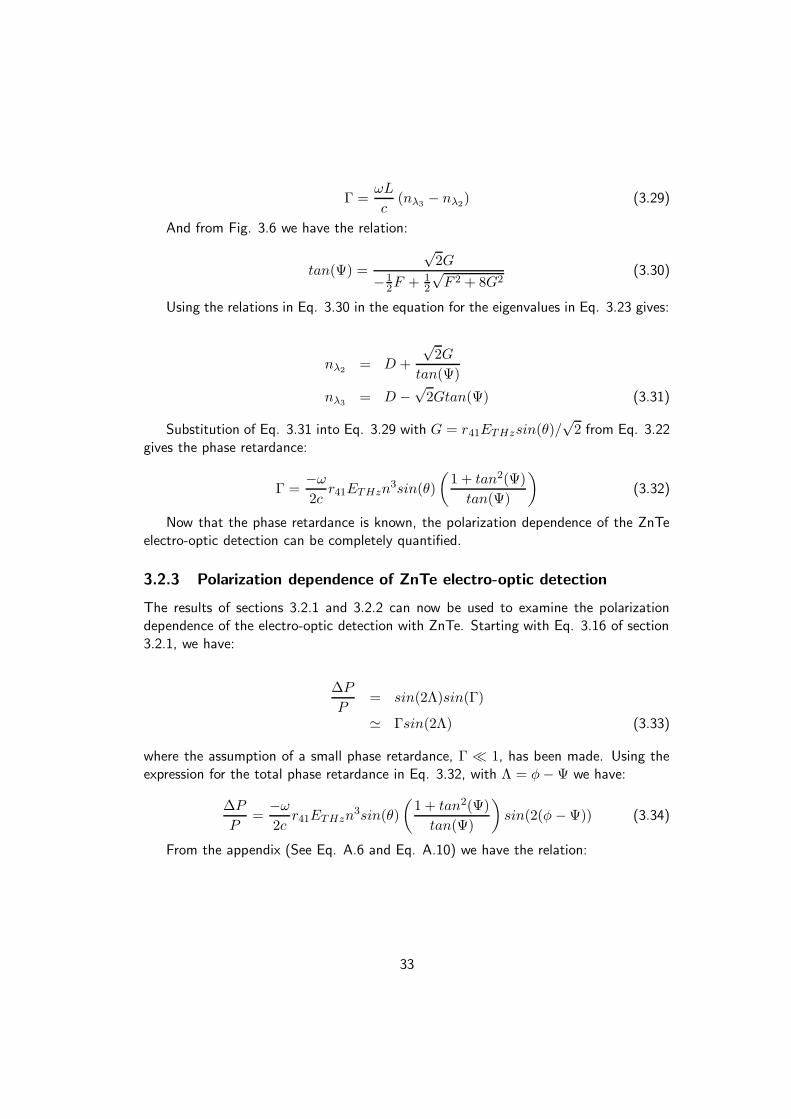
Γ =ωL
c(nλ3
− nλ2) (3.29)
And from Fig. 3.6 we have the relation:
tan(Ψ) =
√2G
−12F + 1
2
√F 2 + 8G2
(3.30)
Using the relations in Eq. 3.30 in the equation for the eigenvalues in Eq. 3.23 gives:
nλ2= D +
√2G
tan(Ψ)
nλ3= D −
√2Gtan(Ψ) (3.31)
Substitution of Eq. 3.31 into Eq. 3.29 with G = r41ETHzsin(θ)/√
2 from Eq. 3.22gives the phase retardance:
Γ =−ω
2cr41ETHzn
3sin(θ)
(
1 + tan2(Ψ)
tan(Ψ)
)
(3.32)
Now that the phase retardance is known, the polarization dependence of the ZnTeelectro-optic detection can be completely quantified.
3.2.3 Polarization dependence of ZnTe electro-optic detection
The results of sections 3.2.1 and 3.2.2 can now be used to examine the polarizationdependence of the electro-optic detection with ZnTe. Starting with Eq. 3.16 of section3.2.1, we have:
∆P
P= sin(2Λ)sin(Γ)
' Γsin(2Λ) (3.33)
where the assumption of a small phase retardance, Γ 1, has been made. Using theexpression for the total phase retardance in Eq. 3.32, with Λ = φ − Ψ we have:
∆P
P=
−ω
2cr41ETHzn
3sin(θ)
(
1 + tan2(Ψ)
tan(Ψ)
)
sin(2(φ − Ψ)) (3.34)
From the appendix (See Eq. A.6 and Eq. A.10) we have the relation:
33

sin(θ)
(
1 + tan2(Ψ)
tan(Ψ)
)
sin(2 (φ − Ψ)) = − (cos(θ)sin(2φ) + 2sin(θ)cos(2φ))
(3.35)Combining Eq. 3.35 and Eq. 3.34 gives the pump and THz polarization dependence
of balanced detection using ZnTe to be:
∆P
P=
ω
2cr41LETHzn
3 (cos(θ)sin(2φ) + 2sin(θ)cos(2φ)) (3.36)
which agrees with the calculation performed by Planken et. al. [49].
3.2.4 ZnTe electro-optic detection as a polarization analyzer
In this section, we will demonstrate that with the appropriate orientation of the ZnTecrystal, and polarization of the probe beam, it is possible to use the ZnTe electro-opticdetector as an analyzer.
We begin with a specific orientation of the [001] crystal axis of the ZnTe crystal inthe lab reference frame, with fixed polarizations of the THz field and the probe beam.The crystal is then rotated about the surface normal (the [0 0 1] crystal axis is rotated),and the response is examined. We do this for two particular configurations of the probeand THz field polarizations shown in Fig. 3.7.
Using this configuration, we can write the equations for the electro-optic signal re-sponse for a horizontally polarized probe and vertically polarized THz field (SHprobe,VTHz
),as well as for a horizontally polarized probe beam and horizontally polarized THz field(SHprobe,HTHz
) as follows:
SHprobe,HTHz= c1 (cos(α)sin(2α) + 2sin(α)cos(2α)) (3.37)
where c1 is a constant. As well, we have:
SHprobe,VTHz= c1 (−sin(α)sin(2α) + 2cos(α)cos(2α)) (3.38)
where these equations were obtained by setting φ = α and θ = α in Eq. 3.36 forSHprobe,HTHz
and φ = α and θ = α + π2 for SHprobe,VTHz
.In order for the ZnTe to behave as a polarization analyzer, we would like to find the
angles where there is a maximum sensitivity to horizontally polarized THz fields, whilesimultaneously having zero response to a vertically polarized THz field and vice versa.In order to examine this question, we tabulate the zeros for the two functions in Table3.1.
Similarly, the extrema for the electro-optic response are tabulated in Table 3.2.Obviously, this is not straight-forward given the complicated nature of the zeros and
extrema in tables 3.1 and 3.2. To aid in visualizing this, we present analytical plots of the
34

α
α + π2
[001]
ETHz
ZnTe
(b)
(a)
ETHz
[001]
α ZnTe
Eprobe
Eprobe
Figure 3.7: Configuration for electro-optic detection of THz radiation with a horizontallypolarized probe beam. Detection of vertically (a) and horizontally (b) polarized THzfields as a function of the angle of crystal rotation α.
35

Table 3.1: Zeros of the polarization response function of the ZnTe electro-optic detector(Equations 3.37 and 3.38).
Zero α(SHprobe,HTHz) α(SHprobe,VTHz
)
1st 0 cos−1(√
23 ) = 35.26o
2nd cos−1( 1√3) = 54.74o π
2 = 90o
3rd cos−1(− 1√3) = 125.26o cos−1(−
√
23) = 144.74o
4th π = 180o π + cos−1(√
23) = 215.26o
5th π + cos−1( 1√3) = 234.74o 3π
2 = 270o
Table 3.2: Extrema of the polarization response function of the ZnTe electro-opticdetector (Equations 3.37 and 3.38).
Extrema α(SHprobe,HTHz) α(SHprobe,VTHz
)
1st cos−1(√
73 ) = 28.13o 0
2nd π2 = 90o cos−1(
√2
3 ) = 61.87o
3rd cos−1(−√
73 ) = 151.87o cos−1(−
√2
3 ) = 118.13o
4th π + cos−1(√
73 ) = 208.13o π = 180o
5th 3π2 = 270o π + cos−1(
√2
3 ) = 241.87o
two functions SHprobe,HTHzand SHprobe,VTHz
In Fig. 3.8. Experimental measurementshave also been made and are plotted in Fig. 3.8 to verify that these results are correct.The experimental data was obtained using a semi-large aperture photoconductive THzemitter, oriented to produce either a horizontally or vertically polarized THz beam at theZnTe crystal, while the probe beam is horizontally polarized. For a detailed descriptionof the experimental set-up, the reader is referred to Chapter 7. The ZnTe crystal isrotated about the [110] crystal axis, and the angular dependence is monitored.
We first note that the angular dependence is described well by the analysis performedabove. In particular, note that the zeros and extremum are as listed in the tables above.It is also clear from the plots and the tabulated zeros and extrema, that there are onlyfour angles of orientation of the ZnTe crystal for which an extrema occurs for one THzpolarization, while simultaneously having zero response for the other THz polarization.These angles are, α = 0, π
2 , π, 3π2 . In order for proper relative measurements of the
polarizations, the magnitudes at each angle for each polarization of the THz beammust have the same sign. Therefore, there are two ways in which the ZnTe electro-opticresponse can be used as a polarization analyzer using a fixed horizontally polarized probebeam. These are: (i) ZnTe at α = 0 for sensitivity to vertically polarized THz emission
36

Figure 3.8: Theoretical and experimental angular dependence of ZnTe orientation for ahorizontally polarized probe beam, and vertically (top, circles) and horizontally (bottom,squares) polarized THz fields. The experimental data was taken with a semi-largeaperture photoconductive switch oriented to produce either horizontally (squares) orvertically (circles) polarized THz emission at the ZnTe crystal.
37

and ZnTe at α = π2 for sensitivity to horizontally polarized THz emission, and (ii) ZnTe
at α = π for sensitivity to vertically polarized THz emission and ZnTe at α = 3π2 for
sensitivity to horizontally polarized THz emission.This important result is used to study the polarization dependence of the emitted
THz radiation in various configurations throughout the remainder of the thesis. Thatis, an external polarizer for the THz radiation is not required. By proper selection ofthe ZnTe orientation, sensitivity to orthogonal THz polarization components can beobtained.
3.3 Examination of the ZnTe electro-optic response
With the qualitative description presented in the previous analysis for the polarizationdependence of the electro-optic response of ZnTe, we can analyze our detected fields inreal units of V
cm , provided that we know the index of refraction and the linear electro-optic coefficient r41. In this section, we will examine the value of r41 obtained in acalibration experiment, and compare it to literature values.
The ZnTe crystals used in reporting results here were obtained from eV products Inc.The samples were single crystal, 1mm thick, 1cm square samples. They had very lowresistivity ( 1kΩ-cm), which made the standard calibration of the electro-optic coefficientextremely difficult as large bias fields, required to induce birefringence, were impossibleto generate without damaging the crystal.
Without a bolometer for absolute power calibration, and with pyroelectric detectorsthat are quite noisy, it was found that a cross-calibration with a high-resistivity crystalof Lithium Niobate was one way to check the calibration of the ZnTe crystal. LithiumNiobate is well-characterized, making it a suitable choice for cross-calibration, and it isrelatively straight-forward to measure the electro-optic coefficient of Lithium Niobatewith DC or low-frequency fields.
In this section, we will first examine the calibration of the DC electro-optic coefficientof the Lithium Niobate crystal, and then proceed to examine the cross-calibration ofZnTe, and finally compare the result to literature values.
3.3.1 Calibration of the electro-optic response of lithium niobate
The lithium niobate crystals used for the calibration measurements were single-crystalx cut crystals 0.5 mm thick. Electrodes were formed on the crystal face, parallel to they axis using silver paint, such that the applied electric field was parallel to the z crystalaxis. LiNbO3 has 3m symmetry, so that the linear electro-optic tensor is given by [60]:
38

rij =
0 −r22 r13
0 r22 r13
0 0 r13
0 r31 0r51 0 0−r22 0 0
(3.39)
Application of an electric field, E, leads to a modification of the indices of refraction,as described in section 3.2.3. For the calibration measurements, the applied field isparallel to the z axis (ie. E = Ez), and leads to the index ellipsoid:
(
1
n2x
+ r13E
)
x2 +
(
1
n2y
+ r13E
)
y2 +
(
1
n2z
+ r33E
)
z2 = 1 (3.40)
where nx = ny = no and nz = ne. Note that the principal axes remain unchanged,however, the magnitude of the index is changed along each principal axis due to theapplication of an electric field along z.
For a beam propagating along x, and polarized in the zy-plane, the phase retardance,Γ is given by:
Γ =ωL
c(ny − nz) (3.41)
where ω is the optical frequency, L is the length of the crystal and c is the speed of light invacuum. From the index ellipsoid, we have: nz ' ne− 1
2n3er33E and ny ' no− 1
2n3or13E.
Inserting this into Eq. 3.41 gives:
Γ =2πL
λ
(
no − ne −1
2n3
or13 +1
2n3
er33E
)
= Γo + ΓE
Γo =2πL
λ(no − ne)
ΓE =πLE
λ
(
n3er33 − n3
or13
)
=πLE
λreff
reff ≡(
n3er33 − n3
or13
)
(3.42)
From Eq. 3.42 it is clear that a measurement of Γ(E) will give reff by evaluatingthe slope of the curve. The experimental configuration is shown in Fig. 3.9. For thecrossed-polarizer geometry of Fig. 3.9, the photodiode signal: PD1/PD2 is given by:
39

Pout
Pin≡ PD1
αPD2= sin2(2θ)sin2
(
Γ
2
)
(3.43)
where α is a correction factor taking into account the relative signal produced by thebeam splitter (BS) in Fig. 3.9. The value of α is obtained by setting αPD2 = PD1when the input polarization is parallel to z (see Fig. 3.9).
The experiments are performed such that the angle θ in Eq. 3.43 is π/4.
PD1
PD2
HeNe
F L Pol
BSPol
LiNbO3
zV +
xyEHeNe
PD1PD2
to electronics
LiNbO3
θ = π/4
Figure 3.9: Experimental set-up for determining the linear electro-optic coefficient oflithium niobate. F is a filter; L is a lens; Pol is a polarizer; PD are photodiodes; BSis a beam splitter (quartz window). The linearly polarized HeNe beam makes an angleθ = π
4 with the y crystal axis. The applied field lies along z. The ratio of input tooutput powers in a crossed polarizer geometry is measured such that the electro-opticcoefficient may be extracted.
Applying the bias field, and extracting the measured phase retardance, ΓE of Eq.3.42, we obtain the results in Fig. 3.10. From the slope of the curve, we obtain the
40

Figure 3.10: Measured phase retardance of a 632.8 nm HeNe laser through a 0.5 mmthick LiNbO3 crystal as a function of the applied bias field. The bias field is appliedparallel to the z crystal axis and the x axis is parallel to the propagation direction of thelaser.
41

effective electro-optic coefficient, reff = 166 ± 5pmV −1 in Eq. 3.42. An additionalcorrection was required to calculate the exact electric field at the center of the crystal forthe layout of the electrodes used. Using FEMLAB 1, it was found that the electric fielddistribution within the LiNbO3 is expected to be approximately 13% smaller than thesimple estimate of E = V/dgap. This results primarily from placing the electrodes onopposite sides of the crystal face to avoid breaking down the air between the electrodesupon applying high voltage. Correcting the effective linear electro-optic coefficient forthe field distribution gives a value of reff = 188 ± 6pmV −1. The error is estimatedfrom the experimental data, and does not include systematic errors that may resultfrom deviations in crystal thickness, or variations in the exact electric field distributionobtained from modeling.
Since a DC field was employed; It should be noted at this point that the low frequencyvalue of the linear electro-optic coefficient (unclamped) , rT
eff , was measured. In fact,the linear electro-optic coefficient has acoustic resonances [61], and it is therefore thelow frequency value with which we need to compare our result. Examining the reportedvalue of the effective linear electro-optic coefficient for low frequencies at an opticalwavelength of 632.8 nm, we find a reported value of rT
eff = 190pmV −1 [62], in excellent
agreement with our measured value of rTeff = 188 ± 6pmV −1. Finally, we note that
for high frequency measurements, the clamped value of the effective linear electro-optic coefficient, rS
eff , should be used. Therefore, for using lithium niobate in THz
experiments, the corresponding high frequency value rSeff = 224pmV −1 should be used
[62].
3.3.2 Comparison of ZnTe and LiNbO3 electro-optic responses
With this value for the effective linear electro-optic coefficient for LiNbO3, it is possibleto perform a cross-calibration of the ZnTe crystal using the terahertz field as a bias.
Preliminary measurements of radiated THz fields using LiNbO3 demonstrated ex-ceptionally high noise levels. This was a result of not being able to properly balance thedetection with a quarter-wave plate due to the intrinsic birefringence of the LiNbO3.To overcome this, measurements with the LiNbO3 were taken with an identical crystalof LiNbO3 in the probe beam path, but oriented orthogonal to the detection crystal,such that the intrinsic birefringence was canceled, allowing proper balancing of the probebeam for differential detection.
A plot of the measured THz field radiated from a large-aperture photoconductiveswitch, with both LiNbO3 and ZnTe oriented for maximal sensitivity, is shown in Fig.3.11. The experimental set-up for this measurement is given in detail in chapter 4.
Recall from section 3.2.2, the differential photo-diode signal for optimal detection,θ = π
2 , which is:
1FEMLAB is a commercial finite element numerical computation package created by COSMOL. Seetheir web-site at www.femlab.com for more details.
42

Figure 3.11: Detected THz field radiated from a large-aperture photoconductive switchas function of probe delay using a 1 mm thick ZnTe crystal (top) or a 0.5 mm thickLiNbO3 crystal (bottom). The signal measured from the ZnTe crystal is multiplied bya factor of 0.2 for clarity.
43

∆P
P=
ω
cr41ETHzLn3 (3.44)
Similarly, for LiNbO3, we expect for small retardance, the differential photodiodesignal to be (Using Eq. 3.42 in Eq. 3.16):
∆P
P=
πLE
2λreff
reff ≡(
n3er33 − n3
or13
)
(3.45)
Taking the ratio of equations 3.44 and 3.45 we obtain the expected ratio of responses:
(
∆PP
)
ZnTe(
∆PP
)
LiNbO3
=2LZnTer41
LLiNbO3reff
= 1.65 (3.46)
Solving for r41, the linear electro-optic coefficient of ZnTe we obtain:
r41 =
((
∆PP
)
ZnTe(
∆PP
)
LiNbO3
)
× LLiNbO3reff
2LZnTe(3.47)
From Fig. 3.11, the measured ratio is 16 ± 2, which is significantly different than1.65 predicted in Eq. 3.46. This is almost entirely due to the difference in group-velocitymismatch of the THz beam and optical probe beam within the two crystals.
Group-velocity mismatch in LiNbO3 and ZnTe has previously been examined indetail in Refs. [63, 64]. The effect of group-velocity mismatch, in the time domain, onthe measured THz signals in Eq. 3.44 and Eq. 3.45 is obtained by setting:
ETHz →∫ L
0
(
ETHz
(z
c∆n + T
)
e−αz)
dz (3.48)
where z is the distance of the beam into the crystals, ∆n is the index mismatch atoptical and far-infrared frequencies, T is the absolute time, and α is the absorptioncoefficient of the crystals, which is assumed to be frequency independent. In addition,the THz field within the crystals will be different due to Fresnel reflection at the crystalinput face. The notation CZnTe and CLiNbO3
will be used for the Fresnel amplitudereflection coefficient. Taking these both into consideration, we rewrite the ratio of Eq.3.47 as:
44

r41 =
((
∆PP
)
ZnTe(
∆PP
)
LiNbO3
)
× LLiNbO3reffCLiNbO3
2LZnTeCZnTe
×
(
∫ L0
(
ETHz
(
zc∆n + T
)
e−αz)
dz)
LiNbO3(
∫ L0
(
ETHz
(
zc∆n + T
)
e−αz)
dz)
ZnTe
(3.49)
The optical (800 nm) and far-infrared (1 THz) indices of refraction used for ZnTeas given by Ref. [65] were 2.85 and 3.17 respectively. The optical (800 nm) indices ofrefraction used for the ordinary and extraordinary indices of refraction for LiNbO3 asgiven by Ref. [66] were 2.26 and 2.17 respectively. The far-infrared (1 THz) indicesof refraction used for the ordinary and extraordinary indices of refraction for LiNbO3
as given by Ref. [67] were 6.7 and 5.15 respectively. This gave values for the indexmismatch in ZnTe of ∆n = nfir − nopt = 0.32. The index mismatch for the LiNbO3
depends on the geometry; in this case, the THz field is parallel to the extraordinary(z) axis, and the probe beam is at 45o relative to the x and z-axes. Therefore theindex mismatch for LiNbO3 is taken as ∆n = nfir − nopt = 2.94. Finally, the valuesfor the power absorption coefficients for the far-infrared radiation in the ZnTe andLiNbO3 crystals are taken as frequency independent with values of 5 cm−1 and 10cm−1, respectively [67]. Numerical evaluation of the correction factor in the squarebraces of Eq. 3.49, assuming an input Gaussian pulse shape with a pulse-width of0.5 ps (FWHM), yields 0.10 ± 0.01. This gives a measured value for r41 in ZnTe ofr41 = 3.9±0.4pm
V , in excellent agreement with reported values for ZnTe between 3.9-4.0pmV [63, 64, 68, 69, 70]. Therefore, for the remainder of the thesis a value of r41 = 3.9pm
Vwill be used.
45

Chapter 4
Comparison of large-aperturephotoconductive switch and InAssurface emission 1
InAs has previously been reported to be an efficient emitter of Terahertz radiation atlow excitation fluences, using femtosecond laser pulses. In an effort to quantify theefficiency of the InAs surface emission, the scaling and saturation of THz emission froma (100) InAs surface as a function of excitation fluence is measured and quantitativelycompared to the emission from a GaAs large-aperture photoconductive switch. In thischapter a brief description of the operation of a large-aperture photoconductive switchwill be presented, followed by a brief discussion of the current understanding of theemission of THz radiation from InAs. Following this, the experimental results from anexperiment where the two emitters were compared will be presented.
4.1 Description of the large-aperture photoconductive switch
The emission of THz radiation from a large-aperture photoconductive switch has beendescribed in detail in Ref. [72]. In this section, the main characteristics associated withthe scaling of the emission will be reviewed.
A large-aperture photoconductive switch is what the name implies: a photocon-ductive switch for which the dimensions are large compared to the wavelength of theemitted radiation. In this case, there exists a current distribution, as a consequence ofillumination with an above band-gap wavelength optical pulse, that has a spatial extentlarger than the characteristic wavelength of the emitted radiation. Darrow et. al [72]showed that in this case, the theoretical treatment was best approached by use of planewaves.
1The results in this chapter have been published in Ref. [71]
46

The boundary conditions on the radiated THz field can be used in conjunction withOhm’s law, to relate the optically injected current density to the radiated field. Theresult is that the relation between the time-varying surface conductivity, applied biasfield and radiated THz field are given by:
Erad(t) = −Ebσs(t)η0
η0σs(t) + 1 +√
ε(4.1)
where Erad(t) is the radiated electric field at the emitter, inside of the substrate, E b isthe applied bias field on the switch, η0 is the impedance of free space, ε is the dielectricconstant and the time-dependent surface conductivity, σs(t), is given by:
σs(t) =e(1 − R)
hν
∫ t
−∞dt′µ(t − t′)Iopt(t
′)e−t−t′
τcar (4.2)
where e is the electronic charge, R is the reflectivity (at normal incidence for the aboveanalysis), hν is the optical photon energy, µ is the time dependent mobility of thesubstrate, Iopt is the intensity profile of the optical excitation pulse and τcar is thecarrier recombination time.
The above model describes the experimentally observed scaling dependence on biasfield and optical excitation fluence in a relatively simple way. In Eq. 4.1, the THz fieldgrows as the conductivity increases, however, it eventually saturates. The value to whichit saturates is the bias field. That is, the THz field cannot exceed the value of the biasfield, and monotonically approaches the bias field (opposite in direction) as the deviceis pumped harder.
In order to demonstrate the dependence on the optical pump energy, we notice thatEq. 4.1 monotonically increases with increasing conductivity. Therefore, the maximumof the radiated field occurs when the conductivity reaches its respective maximum, andis given by:
Epkrad = −Eb
σmaxη0
σmaxη0 + 1 +√
ε(4.3)
where σmax is the maximum of the surface conductivity in time. Further, we assumeDrude conductivity such that σ(t) = µ(t)n(t)e, which assumes that the carrier recom-bination time is significantly larger than the optical excitation pulse width in Eq. 4.2.Finally, if we assume that the mobility is time-independent and given by the DC mo-bility, then the conductivity would simply be σ(t) = µen(t). This assumes that theinjected photon energy is only slightly above the band-gap, which is the case for ourexperiments with the photon energy of 1.55eV in comparison to the band-gap of 1.5 eVfor semi-insulating GaAs.
The time-dependent carrier density, n(t), is given by:
n(t) =(1 − R)
hν
∫ t
−∞Popt(t
′)dt′ (4.4)
47

where Popt(t) is the incident optical power as a function of time. Using the assumptionthat the carrier recombination time is much larger than the optical excitation pulsewidth, the carriers will all be injected before they begin to recombine. Therefore wehave that σmax = µenmax, with nmax = Fopt(1−R)/hν, which gives the peak radiatedfield in Eq. 4.3 to be:
Epkrad = −Eb
e(1−R)µDCFoptη0
hνe(1−R)µDCFoptη0
hν + (1 +√
ε)
= −EbFopt
Fopt + Fsat(4.5)
where Fsat is the saturation flux, defined by:
Fsat =hν(1 +
√ε)
e(1 − R)µDCη0(4.6)
which is equivalent to the saturation flux expression given in Ref. [68]. From equations4.5 and 4.6 it is evident that the radiated THz field will scale linearly with the appliedbias field and saturate with optical excitation fluence, the saturation fluence given byEq. 4.6. These scaling behaviours will be discussed in the next section.
4.2 Direct comparison
In this section the efficiency of InAs as a high-power THz emitter under high excitationfluence is examined. The GaAs large-aperture photoconductive switch (LAPCS) hasbeen used in the past to generate the highest reported conversion efficiency from opticalto pulsed THz radiation [73], and has been used as a benchmark for efficiency of THzemitters [74]. In this section, such a GaAs LAPCS has been used for comparison to gaugethe overall conversion efficiency of InAs. Scaling of emission with excitation fluence andsaturation of emission is presented, and a quantitative comparison to a GaAs LAPCS isreported.
The experimental set-up is similar to that of section 2.1 and is shown in Fig. 4.1.A regeneratively amplified Ti:Sapphire laser system (Spectra Physics Hurricane) is usedas a source, operating at a center wavelength of 800 nm, at 1 kHz repetition rate, witha maximum pulse energy of 750 µJ and a pulsewidth of 130 fs (Gaussian FWHM).The beam is split into pump (92%) and probe (4%) beams using a wedged window.The probe time is varied with respect to the pump using an optical delay line, allowingtime-resolved mapping of the THz field. A variable attenuator (λ/2 plate and polarizer)is used in the pump beam to vary the fluence. The THz radiation from the emitteris collected and imaged onto the detector using 4 F/2 parabolic mirrors in an f-2f-fgeometry to minimize frequency dependent focusing effects [75, 76, 77], and allow a
48

direct comparison of emitted THz fields between the two emitters. The four parabolicmirrors are employed to attain an intermediate focal plane for testing samples, whichis used later in the thesis to study samples of wood. To detect the THz radiation, theprobe is co-linearly propagated through a 1mm thick, (110) ZnTe electro-optic crystal,together with the THz pulse. This induces a polarization modulation, which is ana-lyzed using a polarization bridge (λ/4 plate and Wollaston prism), with the differentialphotodiode signal detected using a lock-in amplifier at the optical chopping frequencyof approximately 330Hz. The orientation of the ZnTe crystal is chosen to maximizethe electro-optic signal as in section 3.2.4. The GaAs emitter used is constructed on ahigh-resistivity GaAs substrate (the carrier concentration and Hall mobility specified bythe manufacturer are nc = 1.5 × 107cm−3 and µH = 3890cm2V −1s−1, respectively).Silver paint was used to define electrodes with a gap spacing of 0.19 cm and biasedat 300 V (1.6 kV/cm). The GaAs emitter is illuminated at normal incidence and thetransmitted THz beam was collected.
The InAs emitter is a (100) oriented, undoped, n-type InAs sample (nc = 1.9 ×1016cm−3, µH = 2.5 × 104cm2V −1s−1) which is illuminated at 45 degrees angle ofincidence. The pump beam is telescoped to a 1/e2 intensity beam diameter of 2.85±0.05mm for both emitters using a pair of lenses as shown in Fig. 4.1.
The orientation of the crystal is such that the projection of the p-polarized pumpbeam on the (100) plane of the InAs crystal is at 450 relative to both the [010] and [001]crystallographic axes, and the p-polarized THz beam is collected. Initial measurementsof the saturation of the signals from InAs were carried out in the absence of magneticfields.
In order to determine the efficiency and saturation of the two emitters, the scaling ofthe THz emission with optical excitation fluence was measured. The fluence is calculatedas the full energy of the pump beam before striking the surface of the emitter, dividedby the 1/e2 (intensity) beam area of 0.064 ± 0.003cm2. The GaAs-LAPCS is orientedin a transmission geometry, such that the pump beam illuminates the switch at normalincidence, while the InAs sample is unbiased, with the bare (100) surface oriented at 450
to the pump beam as shown in Fig. 4.1. The resultant peak measured emitted field asa function of the incident fluence is presented in Fig. 4.2. The peak radiated terahertzfield is taken as the maximum of the absolute value of the time-domain waveform. Theinset of Fig. 4.3 shows waveforms radiated from the LAPCS and InAs sources. The THzsignal from both emitters is observed to saturate as the fluence is increased. The radiatedfield is well described by the simple saturation formula, Epk
THz = BF/(F +Fsat), whereB is a scaling constant, F is the excitation fluence and Fsat is the saturation fluence.The solid curves in Fig. 4.2 are the fits of this equation to the data, and the values forB are 300 ± 30 and 220 ± 22 V/cm and Fsat are 29 ± 4 and 10 ± 1.3 µJ/cm2 for InAsand GaAs respectively. The value for the saturation flux of the GaAs obtained is within30% of the more recently reported results for the saturation flux from GaAs LAPCS[74, 68, 78]. In our case, the GaAs aperture is overfilled, whereas in most reports onsaturation behavior of the GaAs LAPCS, the pump beam diameter is comparable to the
49

aperture dimension.From Fig. 4.2 it is clear that the peak radiated field from the (100) InAs emitter is
larger in the saturated regime, and reaches a saturated field approximately 30% higherthan that for the GaAs LAPCS. In addition, the saturation fluence for InAs is almost 3xlarger than that for the GaAs LAPCS.
With quantification of the scaling of both emitters with excitation fluence, the ques-tion of which emitter most efficiently converts optical to far-infrared energy can beexamined. We can estimate the total energy in the THz pulses, and compute an es-timate for the overall conversion efficiency. The method is outlined as follows. Theconversion efficiency, η, is defined by:
η =
(
WTHz
Winp
)
(4.7)
where the estimated THz pulse energy is:
WTHz ≈τA∣
∣
∣Epk
THz
∣
∣
∣
2
2η0(4.8)
where W represents energy, τ is the 1/e (electric field) THz pulse width, A is the area
of the THz beam at the detector, EpkTHz is the peak radiated THz field and η0 is the
impedance of free space. The definition of the 1/e electric-field THz pulse width isshown in Fig. 4.3. The 1/e pulse-width is taken as the time-span between when theabsolute value of the field first reaches a value of 1/e of the maximum, and then whenit falls to 1/e of the maximum.
Detected fields are corrected for Fresnel reflection at the emitter and detector, TR,and system transmission losses, TS as:
|EpkTHz| ≈
∣
∣
∣EpkTHz
∣
∣
∣TRTS (4.9)
We compute the input optical energy by integrating over the emission aperture:
Winp =
∫∫
aperture
F exciteopt (x, y) dxdy (4.10)
The experimental values used are given in Table 4.1. The THz beam waist at thedetector for the two emitters was measured by scanning the THz beam laterally acrossthe optical probe beam, which is less than 100µm in diameter, and measuring the 1/eTHz electric field diameter. The system loss factor was calculated from the transmissionspectrum of the optically opaque beam block used to block the laser radiation fromhitting the detector, and had a flat frequency response over the bandwidth of bothemitters.
Using the values in Table 4.1, and computing the conversion efficiency as outlined
50

Table 4.1: Parameters used in estimation of optical to far-infrared conversion efficiency
Property GaAs InAs Description
System Loss 1.44 1.44 E-field attenuation factor of beam-blockFresnel Loss 1.42 1.31 E-field Fresnel reflection losses (emitter and detector)
τ(ps) 1.54 0.79 Average measured 1/e pulse widthsTHz spot (cm) 0.342 0.245 Measured 1/e THz field diameters
B (V/cm) 223 294 Measured saturation amplitudeFsat(µJ/cm2) 9.6 29.3 Measured saturation fluence
E(µJ) FA 0.82FA Integral of F(A) over the excitation areaA(cm2) 0.064 0.064 1/e2 Intensity beam area of excitation beam
above, we get the results presented in Fig. 4.4 below.Note that the conversion efficiency for the GaAs is much larger than for InAs due to
a larger THz beam waist at the detector and a longer pulsewidth. The larger THz beamwaist at the detector is likely a result of diffraction from the emitting aperture due tothe longer emission wavelengths, and the reduced emitting aperture for GaAs comparedto the InAs. For our GaAs LAPCS, the maximum conversion efficiency, at a bias field of1.6 kV/cm was about 1.9 × 10⁻⁵, while for InAs it was 2.1 × 10⁻⁶. The best reportedconversion efficiency for a GaAs LAPCS was 1.6 × 10⁻³ at a bias field of 10.6 kV/cm[73]. Given that the THz pulse energy scales quadratically with the bias field [72], thenthe maximum conversion efficiency expected from our LAPCS at 10.6 kV/cm would be0.8×10−3, which is a factor of 2 less than reported by You et. al [73]. This discrepancyis possibly a result of not including group-velocity mismatch in the ZnTe electro-opticdetector (thermal detection was used by You et. al [73]) and diffraction losses due tothe limited collection angle in our system. The measured frequency spectrum from thetwo emitters, at an excitation fluence of 1mJ/cm2 is presented in Fig. 4.5. From Fig.4.5 it is also clear that the InAs emitter is better suited to producing higher frequencyTHz radiation (more efficient above 0.75 THz). Most of the dips in the spectra aredue to water absorption lines in air.
Given that the emission aperture for the LAPCS is 0.19 cm in the horizontal di-rection, and the collection aperture is F/2, the matching frequency is 0.32THz for adiffraction-limited beam diffracting from the aperture and exactly filling the F/2 collec-tion optics (1 e-folding of the peak electric field distribution at the collection aperture),below which we expect the signal will be attenuated. The peak of the measured THzspectra occurs at 0.33 THz (see Fig. 4.5), which also is in agreement with an angu-larly truncated beam cutting off the lower frequency components. Focusing the THzfield from an LAPCS with minimal collection angle losses results in a spectrum with apeak at approximately 0.1THz or less [68]. With larger aperture GaAs-LAPCS emittersmeasured in our laboratory, we have also observed a peak emission frequency close to
51

0.1THz. An approximate estimate of the truncation of the spectrum leading to the0.3THz peak emission frequency observed here indicates that approximately half of theemitted radiation is lost due to diffraction losses of the lower frequencies on the collec-tion optics. Thus our observed peak efficiency is consistent with the peak value reportedby You et. al [73]. It is clear that in this regime the large conversion efficiency for GaAsis a result of extracting energy from the electric bias field and not from the energy inthe laser pulse itself.
While the conversion efficiency for the GaAs LAPCS in Fig. 4.4 can be scaled tohigher bias voltages, the unbiased emission from (100) InAs cannot be scaled further,making it much less efficient at converting optical to far-infrared energy than the GaAsLAPCS. However, the application of a magnetic field at low excitation fluences hasbeen shown to increase the THz emission significantly. In fact, the THz emission powerwas shown to scale quadratically with the applied magnetic field [34], saturating aboveapproximately 3T [79, 80, 81]. The enhancement in the emission has been ascribed tothe deflection of the photo-carrier diffusion current, creating a larger component parallelto the surface which radiates more efficiently and hence increases output radiation [35,36]. For the case where the THz signal is predominantly a result of surface opticalrectification, an applied magnetic field would not have the same dramatic effect. Wehave measured the effect of a 0.7T magnetic field, which results in no more than a 20%change in the peak radiated field when exciting the InAs at a fluence of approximately1mJ/cm2. Assuming quadratic power scaling with magnetic field, that portion of theTHz field that is increasing as the square of the magnetic field is estimated to produceat most a 1.7x increase in THz field strength ( 3x in power) in the present polarizationconfiguration, for a field of 3T at a fluence of 1mJ/cm2. Since the optimal conversionefficiency is obtained for operation at Fsat (see below), the effect of the magneticfield around the saturation fluence is the important parameter. Recent results indicatethat above about 0.2µJ/cm2, the effect of the magnetic field is not as dramatic asat lower fluences [82]. In that work, an applied magnetic field of +1.6T resulted ina constant increase in radiated THz power from InAs surfaces of approximately 2xcompared to the case of no magnetic field, above excitation fluences of approximately0.2 µJ/cm2. Scaling our result observed above, the expected increase at 1.6T, basedon our observation of approximately 20% increase in signal at 0.7T, would be 1.45xincrease in electric field, or 2x increase in power, consistent with these reports. Thus,the large enhancement for InAs due to the application of a magnetic field only occurs forvery weak excitation fluences, well below the saturation fluence. The conclusion is thatwhile the power radiated from the GaAs LAPCS can further be increased by applyinghigher bias fields, the InAs is not expected to be enhanced by more than a factor of 3,with the application of large magnetic fields.
One can show that the high efficiency reported for the LAPCS is close to the theo-retical limit expected for this system. An upper bound on the radiated FIR energy froma LAPCS can be estimated, assuming that the maximum radiated field is given by thebias field. Using the results of Darrow et. al. [72] as summarized above in section 4.1,
52

we have that in the near-field the peak-radiated THz field is given by (Eq. 4.5):
Enear−fieldrad,THz = Eb
(
F
F + Fsat
)
(4.11)
where Fsat is the saturation flux. Using Eq. 4.7, with Winp = A×F , with A being thearea of the emitter which is the same as the size of the emitted THz beam we get:
η =τE2
b
2Fη0
(
F
F + Fsat
)2
(4.12)
And noting that the maximum conversion efficiency occurs at Fsat, using τ ∼ 1psand Fsat = 9.6 µJ/cm2 gives an upper bound on the conversion efficiency at Eb= 10kV/cm of:
η =τE2
b
2η0
(
1
4Fsat
)
= 3.2 × 10⁻³ (4.13)
It can be shown that this estimate is consistent with what is calculated using thepeak electric-field in Eq. 28 of Ref. [83], if the τeff in that equation is chosen tobe the inverse of the radial frequency. The above estimated value is about 2x largerthan reported by You et. al. [73], and 4x larger than the experimental value reportedhere. Again, possible reasons for observing a lower conversion efficiency in our case arenot including the effects of group velocity mismatch in the detection crystal and losinga significant portion of the THz signal outside of the collection angle of the imagingsystem. It is clear, nonetheless, that the generated THz energies are in the range of thetheoretical limit which could be achievable.
In conclusion, the magnitude of the emission from an InAs and a GaAs LAPCSemitter was measured as a function of irradiation fluence. Both emitters saturatedand could be fit using a simple saturation equation, with observed saturation fluencesin terms of incident laser fluences of 29.3 and 9.6 µJ/cm2 for the InAs and GaAsemitters respectively. Correcting the detected peak radiated THz fields for Fresnel lossesand system losses, the peak conversion efficiencies were estimated to be 2.1 × 10⁻⁶
and 1.9 × 10⁻⁵ for InAs and GaAs (1.6kV/cm bias) respectively. Using the expectedquadratic scaling with the bias field up to the breakdown voltage of GaAs of 10kV/cm,the efficiency of the GaAs LAPCS can be considerably enhanced relative to that ofunbiased InAs and approaches the theoretically expected limit based on the bias fieldand saturation flux.
53

LPF
PM
λ2
λ4 PD
POL
ODL MM
PL
BS
PDZnTe WPM
LIA
Ti:SapphireLaser
M
Chopper
PL
NL
M
PMFM
M
PM
PM
V+
(2) (1)
Figure 4.1: Schematic diagram of the THz system used in the experiments. FM is a flipmirror, pol is a polarizer, BS is a wedged beam splitter, PM are parabolic mirrors, QWPand HWP are quarter and half-wave plates respectively, WP is a Wollaston prism, L1and L2 are +50 and -15cm focal length lenses, and LPF is a visibly opaque low passfilter that blocks the fundamental. The emitter used is either an externally biased GaAsphotoconductive switch or a (100) oriented InAs surface. (1) and (2) represent beampaths to InAs and GaAs emitters respectively.
54

Figure 4.2: Detected peak THz field as a function of excitation fluence for the twoemitters used. Open triangles represent signals from GaAs LAPCS biased at 1.6kV/cm,and filled squares represent signals from (100) InAs. The solid lines are least-squaresfits of saturation curves to the data.
55

Figure 4.3: Terahertz time-domain signal radiated from the InAs emitter as a functionof the time-delay (solid) and the absolute value (long-dashed) of the electric-field pulsewith a 1/e pulsewidth of 0.79 ps. This pulse-width is what is used in calculations (seetext for details). The inset shows the waveform radiated from the LAPCS (top) and theInAs (bottom), normalized to their peak values.
56

Figure 4.4: Estimated conversion efficiencies based on Equations 1-4 with parametervalues as given in table 4.1. Dashed curve is for GaAs LAPCS at 1.6 kV cm−1 bias, andsolid curve is for (100) InAs.
57

Figure 4.5: Frequency spectrum of THz fields at detector from the GaAs LAPCS biasedat 1.6 kV/cm (dashed) and the (100) InAs (solid) at an excitation fluence of 1mJ/cm2.
58

Chapter 5
Terahertz radiation from InAssurfaces at high excitation fluences1
As found in chapter 4, the weak dependence of the terahertz emission on an appliedmagnetic field as the excitation fluence is scaled to higher values suggests that there isa different mechanism contributing to the terahertz emission at high fluences than atlow fluences. In this chapter, a detailed analysis of the emission mechanism from InAsat high excitation fluences will be presented.
This chapter is organized as follows. The emission mechanism from InAs (100)surfaces will be introduced, where it is found that emission characteristics are comprisedof at least three main mechanisms. The dominant contribution in the end is found to bean effective surface nonlinearity at high fluences, which can arise in at least two distinctforms.
Following this, the bulk dipole response of zinc-blende crystals will be calculated indetail. In order to understand the nonlinear properties better, comparisons are madeto second harmonic generation measurements showing that the emission of second-harmonic radiation from the InAs surfaces predominantly results from bulk second-harmonic generation.
The calculation of the effective second order nonlinear response resulting fromsurface-electric field induced nonlinearities will be presented next, and shown to matchthe observed dependencies of terahertz radiation from InAs surfaces. Comparing thesecond-harmonic and terahertz emission measurements, the large contribution from sur-face electric-field induced optical rectification is then attributed to a large third-ordersusceptibility.
1Parts of this chapter have been published in Refs. [84] and [85], and accepted for publicationin Physical Review B (Apr., 2005)
59

5.1 Emission mechanism of terahertz radiation from InAs
(100)
Traditionally, THz emission from InAs is reported to be a result of photo-excited carrierdiffusion (photo-Dember effect) [40, 86]. For other wide band-gap materials such asInP and GaAs [87, 41], there is evidence that optical rectification (OR) can contributesignificantly to the generation of THz radiation, which has also been reported for narrowband-gap materials such as InSb [88] and (111) InAs [89]. Recently it has been reportedthat there is a negligible contribution from OR in (100) InAs at low and moderateexcitation fluences [90, 79, 82]. The reduced dependence of the THz emission onmagnetic field at higher excitation fluences as discussed in chapter 4, strongly suggeststhe existence of a mechanism different than photo-carrier effects. In this section, thedependence of the THz radiation on crystallographic orientation and pump-polarizationwill be examined in order to determine the emission mechanism from InAs.
The setup for investigating the emission of terahertz radiation from the InAs (100)surface is the same as the reflection mode emission presented in Fig. 4.1 of section 4.2.A regeneratively amplified Ti:Sapphire laser system generates 800 nm, 1 kHz, 750µJ,130 fs pulses. The variable attenuator (λ/2 plate and polarizer shown in Fig. 4.1) isused in the pump beam to vary the fluence. The polarizer can be removed to allowthe linear polarization angle of the pump to be modified. The THz radiation from theemitter oriented in a reflection geometry is collected and imaged onto the detector using4 F/2 parabolic mirrors. The probe is co-linearly propagated through a 1mm thick, (110)ZnTe electro-optic crystal, with the THz field. This induces a polarization modulationwhich is analyzed using a polarization bridge (λ/4 plate and Wollaston prism), with thedifferential photodiode signal detected using a lock-in amplifier at the optical choppingfrequency of approximately 330 Hz. The orientation of the (001) axis of the ZnTe crystalis varied to measure the electro-optic signal from either p- or s-polarized THz field asdiscussed in section 3.2.4. The InAs emitter is a (100) oriented, undoped, n-type InAscrystal illuminated at an incidence angle of 45o (conduction band carrier density andDC mobility are 1.9 × 1016cm−3 and 2.5 × 104cm2V −1s−1, respectively). The pumpbeam is telescoped to a 1/e2 intensity beam diameter of 2.85 ± 0.05 mm using a pairof lenses and the emitted radiation is collected at an angle of 45o to the surface normalin the specular direction.
The crystallographic orientation of the InAs sample was rotated about the surfacenormal [100], while irradiating the sample with a linearly p-polarized pump beam at anexcitation fluence of approximately 2 mJ / cm2. As seen in Fig. 5.1, the p-polarized out-put consists of large constant component plus a small component with 2-fold rotationalsymmetry. The angularly independent component could be attributed to emission fromthe photo-Dember effect, which should lead to constant p-polarized output, indepen-dent of crystal rotation. It could also be attributed to a transient current resulting fromthe acceleration of photo-generated carriers in the surface electric field. However, this
60

contribution is small compared to the photo-Dember effect in InAs at low fluence [90].For the remainder of the thesis, these two processes will be referred to as photo-carrierrelated effects. It is therefore tempting to attribute the emission to photo-carrier relatedeffects, however, the pump polarization dependence of the terahertz emission will showthis to not be the case.
In order to test the idea that the emission results from photo-carrier related effects,the angle of the linearly polarized pump was also varied, while maintaining the InAscrystal fixed with the [011] axis perpendicular to the plane of incidence. Both the s-and p-polarized terahertz emission was measured as the linear polarization angle of thepump beam was rotated, incident at a fluence of 1.7 mJ / cm2. The result is shown inFig. 5.2. There is a strong 2-fold rotational symmetry, both in the s- and p-polarizedTHz signals. A small part of the angular variation in the p-polarized THz signal can bedue to variations in Fresnel reflectivity with input polarization since there is a differencein the transmission for p- and s-polarized radiation into the InAs (Tp = 0.81 and Ts= 0.57 for n = 3.5 at 800nm and 45o incidence angle). Recall that the p-polarizedTHz emission from the InAs (100) crystal face saturates at a fluence of 29.3µJ/cm2 aswas found in chapter 4, and explicitly shown in Fig. 4.2. It should also be noted thatthe crystal orientation was identical in obtaining the results in Fig. 4.2 and Fig. 5.2.Since the angular dependence shown in Fig. 5.2 was measured at an incident fluence of1.7mJ/cm2, very little reduction in output would be expected for even a factor of tworeduction of pump fluence and thus only a very small part of the rotational anisotropyshown in Fig. 5.2 can be related to Fresnel reflection effects.
Since there can be no s-polarized emission from a dipole radiating normal to a dielec-tric discontinuity [45], as is the case for the photo-carrier related emission mechanisms,the s-polarized THz signal in Fig. 5.2 indicates that there is a significant nonlinearoptical response. Another feature of the results shown in Fig. 5.2 is that the radiateds-polarized THz field is 45o phase shifted from the p-polarized THz signal and exhibitsphase reversal under polarization rotation.
The main features that must be explained by any mechanism responsible for theradiated THz field are: (i) large p-polarized isotropic signal under crystal rotation, (ii)large polarization dependence of s- and p-polarized THz signals under pump polarizationrotation, (iii) 45o relative phase between the data sets of p- and s-polarized THz signalsin Fig. 5.2, and (iv) the change of polarity in the s-polarized THz signal under pumppolarization rotation. As will be discussed later, these can be described satisfactorily bythe emission mechanism being surface optical rectification.
Both terahertz emission from optical rectification and second harmonic generationare similar second-order nonlinear phenomena described by the same second-order sus-ceptibility terms with different responses given by the frequency dependence of thesesusceptibilities. However, the angular dependencies which are dependent on crystalsymmetries will be the same for both processes. For the similar phenomenon of sur-face second-harmonic generation from (100) facets of crystals with 43m symmetry, thes-polarized emitted field is proportional to Epump
s Epumpp , while the p-polarized emitted
61

Figure 5.1: Measured p- (triangles) and s-polarized (squares) terahertz emission as afunction of the crystallographic orientation for a p-polarized pump beam at a fluenceof 2 mJ/cm2 incident on (100) n-InAs surface. The orientation angle on the figure isdefined as the angle that the p-polarized pump beam at the (100) face makes with the[011] crystal direction. The solid curves are fits to the angularly dependent contributionsexpected from bulk optical rectification.
62

Figure 5.2: Measured p- (triangles) and s-polarized (open squares) THz fields as afunction of the angle of the linear pump polarization at an incident fluence of 1.7 mJ /cm2 incident on a (100) n-InAs surface. On the figure, 0o corresponds to a p-polarizedpump beam while 90o corresponds to an s-polarized pump beam. The InAs crystalaxes are such that the [011] axis is perpendicular to the plane of incidence. The solidcurves are fits to the data based on the expected polarization dependencies (see text fordetails).
63

field is proportional to a linear combination of (Epumps )2 and (Epump
p )2 [equation 30 andTable IV of Ref. [91]]. The constants of proportionality depend on the linear opticalproperties and the surface nonlinear tensor elements of the InAs, but not the crystallo-graphic orientation. The emission depends only on pump polarization, consistent withobservations (i) and (ii) above. The fact that there is a small non-zero s-polarizedTHz signal in Fig. 5.1 will be discussed later. The large s-polarized THz signal with achange in polarity and 2-fold rotational symmetry 450 out of phase with the data setfor p-polarized THz radiation is simply described by ETHz
s ∼ Epumps Epump
p , and ETHzp
having a large (Ep)2 and small (Es)2 contribution [equation 30 and table IV of Ref.
[91]], consistent with (iii) and (iv) above.At this point it is worth noting that there are other possible mechanisms that cannot
be ruled out without discussion. These are electric-field induced OR [41] (similar toelectric-field induced SHG [47]), bulk OR, and the quadrupolar nonlinear response ofInAs.
Calculating the bulk contribution for our configuration, which is done in the followingsection, we find that there is no angularly independent term for either crystal or pumppolarization angle rotation (see Tab. 5.3 of section 5.2.1). However, the small signalmodulating the large offset of the p-polarized THz signal of Fig. 5.1 would be consistentwith a small contribution from bulk OR.
Electric-field induced second-harmonic generation or optical rectification is a resultof the near-surface field mixing with the third-order susceptibility resulting in an effectivesecond order response of the material [41, 47]. It is shown later in this chapter thatthe symmetry class and (100) orientation of the InAs dictate that the tensor elementsdescribing the process of electric-field induced effective second order nonlinearity areexactly in the same form as described in Ref. [91] for a pure surface response. Thedescription in [91] is phenomenological in nature, and therefore encompasses the relatedprocess of the effective second order response due to the surface field. It is thereforeimpossible to distinguish between surface electric-field induced optical rectification and apure surface nonlinear optical response with crystallographic orientation and polarizationstudies alone. We will refer to these two processes as the effective second order surfaceresponse of InAs.
Finally, the quadrupolar response of the InAs could lead to a large isotropic contri-bution under crystal rotation as was observed in Fig. 5.1. We rule out this possibilityby noting that there is no 4-fold symmetric contribution observable, and the isotropicand crystallographic angular-dependent contributions from the quadrupolar nonlinearityare expected to be within a factor of 4 of each other in magnitude. This can be shownby calculating the contributions using the index of refraction of InAs and an angle ofincidence of 45o [equation 17 and table II of Ref. [91]].
Therefore, the conclusion is that the dominant emission mechanism at these highfluences is the effective nonlinear surface response of InAs. This may also explain somerecent results that report a reduced dependence of THz signal strength on magneticfield as the excitation fluence is increased [82], as we have also observed in the results
64

presented in chapter 4, since it is expected that the magnetic field predominantly affectsthe directionality of moving charges in the photo-carrier related mechanisms but haslittle effect on the nonlinear surface mechanisms.
The residual offset in the s-polarized THz signal seen in Figures 5.1 and 5.2 cannoteasily be explained by the above mechanisms, however, it is a small contribution as thes-polarized signal ( ∼ 30V/cm ) is only 1/10 of the p-polarized signal ( ∼ 300V/cm), which amounts to a 1 % relative power contribution. The residual effects in thep-polarized signals can also be explained from other generation mechanisms. The 2-foldrotational signal apparent under crystallographic rotation is likely due to bulk opticalrectification, as will be shown later in this chapter. The relative contribution is estimatedto be approximately 13% of the total signal. The offset observed for p-polarized THzsignal in Fig. 5.2 is likely due to photo-carrier related effects. Assuming negligible Fresnelcoupling effects (i.e. the emission is saturated), this contribution is approximately 20%.That the emission is reported to be a result of the photo-Dember effect at low excitationfluences [90, 79] may indicate that the saturation fluences for the photo-carrier relatedeffects are substantially less than that for OR at the surface.
5.2 Bulk electric-dipole radiation
In this section, the bulk electric dipole contribution to the radiated field will be calcu-lated. The results will be shown to be consistent with that observed for optical second-harmonic generation in a reflection geometry from InAs surfaces. The second-harmonicradiation is consistent with the expectation that bulk nonlinear optics dominates theradiation process in materials that lack inversion symmetry.
5.2.1 Calculation of bulk electric-dipole radiation
Crystalline InAs has a zinc-blende structure, possessing 43m symmetry. The second-order susceptibility tensor therefore has only six non-vanishing tensor elements, all of
which are equal: χ(2)xyz = χ
(2)xzy = χ
(2)yzx = χ
(2)yxz = χ
(2)zxy = χ
(2)zyx = d14 [60]. In order to
determine the far-infrared polarization at frequency Ω of the InAs lattice that resultsfrom an optical field at frequency ω, we compute:
P(2)(Ω) = χ(2)bulk(Ω;−ω, ω) : Eopt(−ω)Eopt(ω) (5.1)
It should be noted that the calculation that follows is also sufficient to describe theprocess of second-harmonic generation, as the only difference is that the polarizationof the lattice occurs at the sum frequency (ω + ω = 2ω), whereas the far-infraredgeneration occurs at the difference frequency (ω − ω = Ω ∼ 0). In addition, thecalculation is performed only for the bulk electric dipole contribution, and higher-ordermultipoles are not included.
65

As the second-order polarization depends on the orientation of Eopt(ω) with respectto the crystal axes, it is useful to transform the coordinate system to the beam coordinatesystem [91]. Defining the (s, k, z) coordinate system, such that the s axis is in the surfaceof the crystal and parallel to an input s-polarized pump beam, z is normal to the crystalsurface and k = z × s (see. Fig. 5.3), we can define a rotation matrix, Rxtal, fromcrystallographic coordinates to the beam coordinate system for each of the crystal faces:(111), (110) and (100) studied in the present report. For each of the crystal faces, thecrystallographic coordinate system is rotated such that the z axis is parallel to the [111],[110] and [100] crystallographic axis, respectively. The rotation matrices used for eachof the three crystal faces is given in Tab. 5.1.
InAs ks
Epumpp
Eradp
Erads
z
Epumps
Pump
Figure 5.3: Geometry for polarizations and surface orientation of InAs wafers used in thecalculations. The pump beam is linearly polarized and the s- and p-polarized radiatedfields are examined.
For the bulk contribution to the radiated field, we are interested in the dependenceof the THz field amplitude under crystal rotation about the surface normal. We defineanother rotation matrix, Rrot(φ), that defines the angle of rotation of the crystal aboutits surface normal, as well as the total transformation, Rtot as follows:
66

Table 5.1: Rotation matrices to bring crystal coordinates to beam coordinate system
Rotation matrices
(100) crystal face where the [011] axis is parallel to s
R(100)rot =
0 1√2
− 1√2
0 1√2
1√2
1 0 0
(110) crystal face where the [110] axis is parallel to s
R(110)rot =
− 1√2
1√2
0
0 0 11√2
1√2
0
(111) crystal face where the [211] axis is parallel to s
R(111)rot =
√
23 − 1√
6− 1√
6
0 1√2
− 1√2
1√3
1√3
1√3
Rφrot =
sin(φ) −cos(φ) 0cos(φ) sin(φ) 0
0 0 1
(5.2)
Rtot = RrotRxtal (5.3)
For the (111) crystal face, φ is defined as the angle between the k axis and thecrystal [211] axis. For the (110) face, φ is defined as the angle between the k axis andthe crystal [110] axis. For the (100) crystal face, φ is defined as the angle between k andthe crystal [011] axis. The positive direction of rotation is taken as counter-clockwisewhen looking outside from the surface along the direction of the z axis. From this, wecan compute the susceptibility tensor in the beam coordinate system as a function of φby applying the tensor transformation properties of a third rank tensor, and using thetotal transformation Rtot in Eq. 5.3:
67

χ(2)ijk(φ) =
∑
lmn
(
Rtotil Rtot
jmRtotknχ
(2)lmn
)
(5.4)
Recall that the susceptibility tensor, in contracted notation, is given by [60]:
χ(2)ijk =
χxxx χxyy χxzz χxyz = χxzy χxxz = χxzx χxxy = χxyx
χyxx χyyy χyzz χyyz = χyzy χyxz = χyzx χyxy = χyyx
χzxx χzyy χzzz χzyz = χzzy χzxz = χzzx χzxy = χzyx
(5.5)
and that the second order susceptibility tensor for the 43m symmetry group beforetransformation is given by:
χ(2)ijk =
0 0 0 d14 0 00 0 0 0 d14 00 0 0 0 0 d14
(5.6)
For each element of the contracted susceptibility given in Eq. 5.5, the transformationof Eq. 5.6 is computed based on Eq. 5.4. For example, after simplification, the elementχxxx is given by:
χxxx(φ)
d14= 6Rtot
xxRtotxy Rtot
xz (5.7)
The list of all tensor elements under transformation is given in the appendix A.2,Eq. A.11.For each of the crystal faces, each of the 18 elements in Eq. 5.5 is computedusing Eq. 5.4, and the transformed tensors are given in Table 5.2.
Now that the proper transformations have been derived, the lattice polarizationcan be obtained. That is, Eq. 5.1 can be evaluated with the expressions for thesusceptibilities in Table. 5.2 for each of the three crystal faces. However, before thecalculation can proceed, the optical fields within the medium must be known. Referringto Fig. 5.4, the pump fields are given by:
Eins,pump = tsE
outs,pump ≡ tsEs
Eink,pump = tpfcE
outp,pump ≡ tpfcEp
Einz,pump = tpfsE
outp,pump ≡ tpfsEp (5.8)
where,
68

Table 5.2: Electric dipole susceptibility tensor, χ(2)(φ), in the transformed coordinatesystems
Transformed susceptibilities
(100) crystal face
0 0 0 −2d14sin(2φ) d14cos(2φ) 00 0 0 −d14cos(2φ) −2d14sin(2φ) 0
d14cos(2φ) −d14cos(2φ) 0 0 0 −d14sin(2φ)
(110) crystal face
3d14cos(φ)sin(φ)2 d14
4 (cos(φ) + 3cos(3φ)) −d14cos(φ)−d14(sin(φ) − 3sin(3φ)) −3d14cos
2(φ)sin(φ) d14sin(φ)0 0 0
∣
∣
∣
∣
∣
∣
∣
∣
∣
∣
∣
∣
0 0 −d14
4 (sin(φ) − 3sin(3φ))
0 0 d14
4 (cos(φ) + 3cos(3φ))d14sin(φ) −d14sin(φ) 0
(111) crystal face
−√
23d14sin(3φ)
√
23d14sin(3φ) 0 0 d14√
3−√
23d14cos(3φ)
−√
23d14cos(3φ)
√
23d14cos(3φ) 0 d14√
30
√
23d14sin(3φ)
−d14√3
−d14√3
2d14√3
0 0 0
fs =sin(Φ)
n
fc =√
1 − f2s
tp =2 cos(Φ)
n cos(Φ) + fc
ts =2 cos(Φ)
cos(Φ) + nfc(5.9)
where ts and tp are the Fresnel transmission coefficients and fs and fc would be thesine and cosine of the angle inside of the medium (Φ′ of Fig. 5.4) if n were real. Usingthese definitions, we may therefore write the total polarization of the medium due to
69

n
Φ
Eouts,pump
Eoutp,rad
Einp,rad
Eoutp,pump
Eouts,rad
InAs
Eins,rad
Einp,pump
Eins,pump
Θ
Θ′
Φ′
Figure 5.4: Geometry for the calculation involving the transmitted pump fields into andthe radiated fields out of the nonlinear medium. The angle Φ is the angle of incidencewith respect to the surface normal, n, and the angle Θ is the generated radiationpropagation direction taken to be the specular direction.
70

the incident optical field as:
P(2)NL ≡
Ps
Pk
Pz
= χ(2)(φ) :
t2sE2s
t2pf2c E2
p
t2pf2s E2
p
2t2pfsfcE2p
2tstpfsEsEp
2tstpfcEpEs
(5.10)
Using table 5.2 combined with equation 5.10, we obtain explicit expressions for eachindependent component of the lattice polarization in the beam coordinate system, i.e.Ps,Pk and Pz , for each of the three crystallographic faces. This requires some algebra,resulting in relatively long expressions. These are given in appendix A.2, in Eq. A.12.
With the expressions for the three independent lattice polarizations, for each ofthe crystal faces, we may now derive expressions for the radiated field, either second-harmonic or far-infrared emission. To do this, we introduce the notation from Hubner[92] and write:
Es,rad(Ω) = AsΩLeffP bulks (5.11)
and:Ep,rad(Ω) = ApΩLeff(FsPz − FcPk) (5.12)
where we have written the expressions for far-infrared radiation, Ω, however, they holdequally well for second-harmonic generation at frequency 2ω. In this case Fs and Fc
would be the sine and cosine of the angle of the generated radiation within the medium(Θ′ of Fig. 5.4), and Ap and As are as defined in Hubners paper [92], which are allgiven by:
Fs =sin(Θ)
N
Fc =√
1 − F 2s
AS =2πTs
cos(Θ)
Ap =2πTp
cos(Θ)
Tp =2 cos(Θ)
N cos(Θ) + Fc
Ts =2 cos(Θ)
cos(Θ) + NFc(5.13)
where N is the index of refraction for the generated radiation within the nonlinear
71

medium.Taking the appropriate expressions for each crystal face from Table 5.2, and using Eq.
5.1 together with equations 5.12 and 5.11 we may obtain the results for the differentpolarization combinations. For example, substituting in Es = 0 in the polarizationexpressions and computing Eq. 5.12 yields the results for the p-in p-out polarizationgeometry, whereas substituting Es = 0 in Eq. 5.11 yields the p-in s-out geometryand so on. The results are tabulated in table 5.3, where Ω is either the far-infrared orsecond-harmonic frequency, depending on the situation of interest.
Table 5.3: THz or SH field strengths for different polarization combinations. Combina-tions are listed as Ein,out.
Bulk dipole nonlinear response
(111) crystal face
ETHzp,p = 1√
3ApLeffΩd14t
2pE
2p×
[(
2Fsf2s − Fsf
2c + 2Fcfsfc
)
−(√
2Fcf2c
)
cos(3φ)]
ETHzp,s =
√
23AsLeffΩd14t
2pf
2c E2
psin(3φ)
(100) crystal face
ETHzp,p = ApLeffΩd14t
2pE
2p
[
2Fcfsfc − Fsf2c
]
cos(2φ)
ETHzp,s = −2AsLeffΩd14t
2pE
2pfsfcsin(2φ)
(110) crystal face
ETHzp,p = ApLeffΩd14t
2pE
2p×
[(
2Fsfsfc − Fcf2s − 3
4Fcf2c
)
sin(φ) + 34Fcf
2c sin(3φ)
]
ETHzp,s = AsLeffΩd14t
2pE
2p
[(
14f2
c − f2s
)
cos(φ) + 34f2
c cos(3φ)]
5.2.2 Measurements of optical second-harmonic generation from InAs
Optical second-harmonic generation (SHG) from the InAs samples was investigated asa function of crystallographic orientation and for three crystal faces: (100), (110) and(111). The optical pump source used was identical to the experiments involving THzradiation (Spectra-physics Hurricane), and the set-up is shown schematically in Fig. 5.5.The Ti:Sapphire pump laser beam was passed through a polarizer to select p-polarized
72

pump and was incident at 45o on the InAs samples. The pump fluence was adjusted toapproximately 1mJ/cm2 incident on the sample surfaces. A low-pass filter was used toblock the second harmonic leakage from the laser system prior to striking the samplesurfaces. The reflected SH radiation at 400 nm wavelength was collected using a 7.5 cmfocal length lens and passed through a high-pass filter to block the fundamental beam.A UV-polarizer was used to pass only the p-polarized or s-polarized second harmonicradiation at 400 nm to a Hamamatsu R7518 photo-multiplier tube, which was in turnblocked by a 400 nm interference filter to remove any further leakage of the 800 nmfundamental beam.
Lens LP Filter
InAs
Lens
IF Filter
HP Filter
λ2
φ
n
PMT
Pol
Pump
Pol
Figure 5.5: Experimental set-up for SHG measurements. Pol are polarizers; LP Filter isa low-pass filter; HP Filter is a high-pass filter; IF Filter is an interference filter; PMTis a photo-multiplier; λ
2 is a half-wave plate. The InAs samples are rotated about theirsurface normal (n) by an azimuthal angle φ.
The samples are rotated about their surface normal, and the SH intensities aremeasured as a function of the azimuthal angle φ. The results are shown in Fig. 5.6.
Note that the SH intensity as a function of the azimuthal angle φ is describedvery well by the solid curves in Fig. 5.6, which are fits to the data based on the
73

Figure 5.6: Azimuthal dependencies of SHG from (100), (110) and (111) faces of n-InAscrystals at approximately 1mJ/cm2 excitation fluence for p-polarized pump radiation.The solid curves represents fits to the data expected for the bulk electric-dipole contri-bution using the results in Table 5.3. Filled circles represent p-polarized SH intensity,and open circles represent s-polarized SH intensity. The azimuthal angle is defined asthe angle that the projection of the pump beam in the surface plane of the crystal (kin Fig. 5.3) makes with the [011], [110] and [211] crystal axes for the (100), (110) and(111) crystal faces respectively. The plots are shown in the same scale.
74

appropriate azimuthal dependencies listed in Table 5.3, expected for a bulk electricdipole contribution to the SH radiation. In general, for crystals that lack inversionsymmetry, it is expected that the bulk electric dipole contribution to the SH radiationdominates any contribution from the surface terms [93, 94, 95, 96].
We can verify that the azimuthal dependencies are as expected from Table 5.3,by least squares fitting the derived angular functions to the data. For the (111)and (110) crystal faces these are (with the notation Iinput,output): ISH,111
pp = (a1 +
b1cos(3φ))2, ISH,111ps = (a2sin(3φ))2, ISH,110
pp = (a3sin(φ)+b3sin(3φ))2, and ISH,110ps =
(a4cos(φ) + b4cos(3φ))2. The coefficients that were obtained by fitting were: a1 =1.5 ± 0.1, b1 = 8.8 ± 0.2, a2 = 7.6 ± 0.2, a3 = 8.0 ± 0.2, b3 = 7.7 ± 0.2, a4 = 2.0 ± 0.1,and b4 = 6.9±0.2. The error in the measured values is taken as the 3 σ fitting error ob-tained by fitting the data using SigmaPlot2. Tabulating some of the coefficient ratios inTable 5.4 together with the expected theoretical values, we find good agreement betweenexperiment and theory. The values for the index of refraction used in the calculationsfor the optical pump and second-harmonic wavelengths were: nopt = 3.108+ i1.957 andn2ω = 3.714 + i0.432, respectively [97].
Table 5.4: Measured and calculated values for ratios of the coefficients in the fittingfunctions. The ratios are obtained by using the fitting functions and the functionaldependence of the radiation on the angle φ from Table. 5.3. Error bars on the measuredvalues are 3 σ errors in this case.
Expected Calculated Measureda3
a4
=Tp
Ts
2Fsfcfs−Fcf2s− 3
4Fcf2
c1
4f2
c −f2s
4.1 4.0 ± 0.2
b3b4
=TpFc
Ts1.20 1.12 ± 0.04
a3
b3=
2Fsfcfs−Fcf2s − 3
4Fcf2
c3
4Fcf2
c
0.97 1.04 ± 0.04
a4
b4=
1
4f2
c −f2s
3
4f2
c
0.29 0.29 ± 0.02
b1b4
= −√
23
4TpFc
3Ts1.32 1.28 ± 0.05
a2
b3= −
√
23
4Ts
3TpFc0.90 0.99 ± 0.04
b1a4
= −√
23
Tp
Ts
Fcf2c
1/4f2c −f2
s4.6 4.3 ± 0.2
a2
a3
= −√
23
Ts
Tp
f2c
2Fsfsfc−Fcf2s −3/4Fcf2
c0.92 0.95 ± 0.03
The quantities Ts and Tp in Table 5.4 are as defined in Eq. 5.13 of section 5.2.1and are simply the SH Fresnel transmission coefficients from the InAs into air for the s-and p-polarized SH respectively. Similar results are obtained for the (100) crystal face,however a larger deviation from the calculated values was found ( 20%). This deviation
2SigmaPlot is a commercial data-analysis software package
75

was a result of changing the photo-multiplier bias voltage to increase the measuredSH signals for the InAs (100) leading to some variations in the photomultiplier gaincoefficient.
The conclusion here is that, as expected for crystals that lack inversion symmetry,the optical second-harmonic radiation is a result of the bulk nonlinear optical responseof the InAs.
5.3 Electric-field induced nonlinearity
In this section, the effective second-order nonlinearity of InAs that results from a DCelectric-field through the third-order nonlinear susceptibility is examined in detail. Theresults are calculated in the context of surface electric-field induced optical rectification.The calculations demonstrate that surface-electric field induced optical rectification haveexactly the same dependence on pump polarization and crystallographic orientation asa pure surface response in cubic materials. The emission of terahertz radiation fromvarious crystal faces of InAs is shown to be consistent with surface electric-field inducedoptical rectification at high optical excitation fluences.
5.3.1 Calculation of surface electric-field induced optical rectification
The third order susceptibility tensor for zinc-blende crystals with 43m symmetry, χ(3)ijkl,
has only 21 nonzero elements, 4 of which are unique: χ(3)iijj, χ
(3)ijij, χ
(3)ijji and χ
(3)iiii [98].
This can lead to an effective second order nonlinearity, χ(2)effijk , if a DC field is involved.
In the present case, we consider a surface field in the z direction normal to the surface,resulting from the space-charge layer at the InAs / air interface. Following Germer et al.
[47], the effective nonlinear susceptibility, χ(2)effijk , in the electric dipole approximation,
can be expanded in terms of the surface electric field, Esurfz , as:
χ(2)effijk = χ
(2)ijk(Ω;−ω, ω) + 3χ
(3)ijkz(Ω;−ω, ω, 0)(Esurf
z )
+ 6χ(4)ijkzz(Ω;−ω, ω, 0, 0)(Esurf
z )2 + O((Esurfz )3) (5.14)
Considering only the term of first-order in the surface field (i.e. the second term onthe LHS of Eq. 5.14), we can write the effective surface electric field (SEF) induced
second-order response of the system, χ(2)SEFijk as:
χ(2)SEFijk = 3χ
(3)ijkz(Ω;−ω, ω, 0)Esurf
z (5.15)
To properly examine the effective second-order surface response, we transform thesusceptibility tensor to beam coordinates (as done in sec. 5.2.1), so that the surface
76

field lies along the z axis (see Fig. 5.3). The rotation matrices for the three crystalfaces considered here are listed in section 5.2.1 in Tab. 5.1.
Using the transformation properties of a fourth rank tensor:
χrotαβγδ =
∑
lmno
Rrotαl Rrot
βmRrotγn Rrot
δo χ(3)lmno, (5.16)
contracted with the surface field, we expect the form of the effective SEF inducedsecond-order tensor to be:
χ(2)SEFαβγ = 3Esurf
z
∑
lmno
Rrotαl Rrot
βmRrotγn Rrot
zo χ(3)lmno (5.17)
Applying the appropriate rotation matrix, from Tab. 5.1, and evaluating each in-dependent tensor element of Eq. 5.5 (18 in total), the transformed susceptibilities can
be found. For example, the χ(2)SEFxxx component of the electric field induced nonlinear
tensor is given by:
χxxx = χ(3)iijj(RxxRxxRxyRzy + RxxRxxRxzRzz + RxyRxyRxxRzx)
+ χ(3)iijj(RxyRxyRxzRzz + RxzRxzRxxRzx + RxzRxzRxyRzy)
+ χ(3)ijij(RxxRxyRxxRzy + RxxRxzRxxRzz + RxyRxxRxyRzx)
+ χ(3)ijij(RxyRxzRxyRzz + RxzRxxRxzRzx + RxzRxyRxzRzy)
+ χ(3)ijji(RxxRxyRxyRzx + RxxRxzRxzRzx + RxyRxxRxxRzy)
+ χ(3)ijji(RxyRxzRxzRzy + RxzRxxRxxRzz + RxzRxyRxyRzz)
+ χ(3)iiii(RxxRxxRxxRzx + RxyRxyRxyRzy + RxzRxzRxzRzz) (5.18)
All 18 elements of the susceptibility tensor are found in the same way, for each of thecrystallographic faces studied here. The results are listed in appendix A.3 in equationsA.13 to A.30.
Looking at each of the crystallographic faces separately, the transformed effectivesecond order susceptibilities are found. The tensor for the (111) crystal face is given by:
(
χ(2)SEFxyz
)
(111)=
∂11 −∂11 0 0 ∂15 00 0 0 ∂15 0 −∂11
∂31 ∂31 ∂33 0 0 0
(5.19)
where we have:
77

∂11 =Esurf
z√2
(
−χ(3)iijj − χ
(3)ijij − χ
(3)ijji + χ
(3)iiii
)
∂15 = Esurfz
(
2χ(3)iijj − χ
(3)ijij − χ
(3)ijji + χ
(3)iiii
)
∂31 = Esurfz
(
−χ(3)iijj − χ
(3)ijij + 2χ
(3)ijji + χ
(3)iiii
)
∂33 = Esurfz
(
2χ(3)iijj + 2χ
(3)ijij + 2χ
(3)ijji + χ
(3)iiii
)
(5.20)
It should be noted that, in general, the only symmetry conditions that can be ap-plied in the present case, due to above-band-gap excitation, and without knowing allthe system resonances, is that of intrinsic permutation symmetry [60]. Given that wehave optical frequency ω, far-infrared frequency Ω, and the SEF at zero frequency
(χ(3)ijkl(Ω;ω,−ω, 0)), the intrinsic permutation symmetry allows interchanging the sec-
ond and third indices, which will reduce the independent susceptibility elements to 3:
χ(3)iiii, χ
(3)ijij(= χ
(3)iijj) and χ
(3)ijji. If the far-infrared frequency, Ω ∼ 0, is approximated
as a DC field, and overall permutation symmetry holds, the number of independent
susceptibility elements will be 2: χ(3)iiii and χ
(3)ijij(= χ
(3)iijj = χ
(3)ijji).
Similarly, applying the appropriate transformation matrices to the (110) and (100)crystal faces, we obtain the effective SEF induced second order susceptibility as:
(
χ(2)SEFxyz
)
(110)=
0 0 0 0 ∂15 00 0 0 ∂24 0 0
∂31 ∂32 ∂33 0 0 0
(5.21)
where we have:
∂15 =3Esurf
z
2
(
χ(3)iijj − χ
(3)ijij − χ
(3)ijji + χ
(3)iiii
)
∂24 = 3Esurfz χ
(3)iijj
∂31 =3Esurf
z
2
(
−χ(3)iijj − χ
(3)ijij + χ
(3)ijji + χ
(3)iiii
)
∂32 = 3Esurfz χ
(3)ijji
∂33 =3Esurf
z
2
(
χ(3)iijj + χ
(3)ijij + χ
(3)ijji + χ
(3)iiii
)
(5.22)
And finally for the (100) crystal face:
78

(
χ(2)SEFxyz
)
(100)=
0 0 0 0 ∂15 00 0 0 ∂15 0 0
∂31 ∂31 ∂33 0 0 0
(5.23)
where we have:
∂15 = 3Esurfz χ
(3)iijj
∂31 = 3Esurfz χ
(3)ijji
∂33 = 3Esurfz χ
(3)iiii (5.24)
At this point we note that the tensors in Eq.’s 5.19,5.21 and 5.23 are identical in formto the tensors representing a pure surface nonlinear optical response for cubic materials[91]. In addition, it should be noted that the tensor elements are not the same for
different crystal faces; that is, ∂(100)31 6= ∂
(110)31 , for example. The expected dependence
of SH or THz radiation on azimuthal angle is thus found to be functionally identical tothat listed in the paper by Sipe et al. [91]. Following the above derivation for the bulkfields, the effective susceptibility is used to evaluate the nonlinear polarization. Withthis, the radiated fields are found in exactly the same way as for the bulk. The resultsare listed in Table 5.5.
The coefficients fs, fc, ts, tp, As, Ap, Fs, and Fc in Table 5.5 are as defined previouslyin section 5.2.1 in equations 5.13 and 5.9, and Leff is the effective depth of the mediumfrom which the medium polarization contributes to harmonic radiation. Note that ∂ij
of the different crystal orientations are not equivalent and are given by equations 5.20,5.22 or 5.24 according to the crystal orientation. The angle φ is defined in the sameway as in section 5.2.
One finds that the form of the susceptibility tensor for the SEF induced effectivesecond-order nonlinear response is identical to that of an intrinsic surface response [91],but clearly differs from the bulk optical nonlinear response given in Table 5.3. Therefore,in general, crystal rotation measurements alone will not be able to distinguish betweenthese two responses.
5.3.2 Terahertz emission from InAs
The experimental set-up for investigating the THz emission from the InAs samples isshown in Fig. 5.7. A regeneratively amplified Ti:Sapphire laser system (Spectra PhysicsHurricane) is used as a pump source, operating at a center wavelength of 800 nm, at1 kHz repetition rate, with a maximum pulse energy of 750 µJ and a pulse width of120 fs (Gaussian full width at half maximum). The variable attenuator (λ/2 plate andpolarizer) is used in the pump beam to vary the fluence. The THz radiation from thesurface of the sample oriented at 45o angle of incidence is collected in the specular
79

Table 5.5: THz field strengths for different polarization combinations. Combinationsare listed as Ein,out.
Surface electric field induced nonlinear response
(111) crystal face
ETHzp,p = ApLeffΩE2
pt2p[
Fsf2c ∂31 + Fsf
2s ∂33 − 2Fcfsfc∂15
]
−ApLeffΩE2
pt2p[
Fcf2s ∂11
]
cos(3φ)
ETHzp,s = AsLeffΩE2
pt2pf2c ∂11sin(3φ)
(100) crystal face
ETHzp,p = ApLeffΩE2
pt2p[
−2∂15Fcfsfc + Fsf2c ∂31 + Fsf
2s ∂33
]
ETHzp,s = 0
(110) crystal face
ETHzp,p = ApLeffΩE2
pt2p[
Fsf2s ∂33 + Fsf
2c ∂32 − 2Fsfcfs∂24
]
+
ApLeffΩE2pt2p[
12Fsf
2c (∂31 − ∂32) − Fsfsfc (∂15 − ∂24)
]
+
ApLeffΩE2pt2p[
12Fsf
2c (∂31 − ∂32) − Fsfcfs (∂15 − ∂24)
]
cos(2φ)
ETHzp,s = AsLeffΩE2
pt2pfsfc (∂15 − ∂24) sin(2φ)
direction and imaged onto the ZnTe detector using four F/2 parabolic mirrors. A 1mm thick ZnTe (110) electro-optic crystal is used as detector/analyzer, which can beoriented either for sensitivity to p-polarized THz emission, or to the s-polarized THzemission as described in section 3.2.4.
The InAs samples were mechanically polished, nominally undoped, n-type single crys-tals of 0.5 mm thickness. The InAs (111), (110) and (100) samples had intrinsic carrierconcentrations of approximately 3 × 1016cm−3, 1.9 × 1016cm−3 and 2.8 × 1016cm−3,respectively. The carrier mobilities for the InAs (111), (110) and (100) samples wereapproximately 20 000 cm2/Vs, 22 000 cm2/Vs and 19 000 cm2/Vs, respectively. Allvalues are those specified by the manufacturer.
The InAs samples were rotated about their surface normals, and the measured THzsignals recorded as a function of the azimuthal orientation. The results are presented inFig. 5.8.
The emission characteristics from each of the crystallographic faces will be discussedindividually. First, the emission from the InAs (100) crystal face is re-plotted from
80

LIA
PD
PD
ZnTe
LPF
M
Ti:Sapphire Laser
PL
NL
Chopper
InAs WPλ
4
PM
PM
ODL
POL
M
PL
BSλ
2
M
PM
PM
M
Figure 5.7: Experimental set-up for THz experiments. M are mirrors; BS is a beamsplitter; λ
2 is a half-wave plate; PL are positive lenses; NL is a negative lens; PM are
parabolic mirrors; λ4 is a quarter-wave plate; LPF is a low-pass filter; PD are photodiodes;
LIA is a lock-in-amplifier; WP is a Wollaston prism; ODL is an optical delay line. Thearrows represent the beam propagation directions.
81

Figure 5.8: Azimuthal dependencies of THz generation from (100), (110) and (111)faces of n-InAs crystals at approximately 1 mJ/cm2 excitation fluence for p-polarizedpump radiation. Filled circles represent detected p-polarized THz fields, and open circlesrepresent s-polarized THz fields. The azimuthal angle is defined as the angle that theprojection of the pump beam in the surface plane of the crystal (k in Fig. 5.3) makeswith the [011], [110] and [211] crystal axes for the (100), (110) and (111) crystal facesrespectively. The solid curves are fits to the data for p-polarized THz emission, whiledashed curves are the fits to the data for s-polarized THz emission expected for surface-field induced optical rectification as listed in Tab. 5.5.
82

section 5.1 for comparison to the other crystal faces. In section 5.1, it was concludedthat, while the emission characteristics may indicate that photo-carrier related effectsdominate the emission, polarization dependencies (ie. Fig. 5.2) discount this possibility,and demonstrate that the dominant emission mechanism of THz radiation from the(100) crystal face is consistent with surface electric-field induced optical rectification.
Next we discuss the case of the (110) crystal face. Possibly the most clear evidencefor the dominant contribution to THz radiation from surface optical rectification fromInAs is the crystallographic dependence of the THz radiation from the (110) crystal facein Fig. 5.8. There are three observations that can be made from the results presentedin Fig. 5.8 for the (110) crystal face. First, the existence of a significant angularlyindependent contribution to the radiated terahertz field exists. Second, the angulardependence is not what should be expected for bulk optical rectification as outlined intable 5.3. Finally, the angular dependence matches that expected for surface electric-field induced optical rectification as outlined in table 5.5 shown as solid and dashedcurves for the p- and s-polarized THz emission in Fig. 5.8, respectively. However, aclear systematic deviation from the theoretical curve is obvious in the measured datafor the (110) crystal face of Fig. 5.8. Each of these points will be examined nextindividually.
The angularly independent contribution to the radiated terahertz field may resultfrom photo-carrier contributions to the radiated terahertz field as discussed previouslyin section 5.1. Given that the magnitudes of the radiated terahertz field from the (110)and (100) crystal faces are similar, and that the contribution from photo-carrier relatedeffects radiated from the (100) crystal face was estimated to be only approximately 20%as revealed by pump polarization studies in section 5.1, the majority of the angularlyindependent contribution to the terahertz field for the (110) crystal face is attributedto the angularly independent contribution from surface electric-field induced opticalrectification. From table 5.5, the p-polarized radiated terahertz field is expected to beof the form: ETHz
p ∝ c1 + c2cos(2φ). Therefore an angularly independent contributionis expected for the p-polarized terahertz emission from the (110) crystal face due tosurface electric-field induced optical rectification. A small contribution to this angularlyindependent contribution from photo-carrier effects may be present as was observed forthe (100) crystal face in section 5.1.
The bulk optical rectification contribution to the radiated terahertz field is predictedto be of the form: ETHz
p ∝ c1sin(φ)+c2sin(3φ) from table 5.3. Clearly, this dependenceon orientation is qualitatively not observed. In fact, the solid curve for the (110) crystalface in Fig. 5.8 is a least squares fit to the data based on a dependence of the form:ETHz
p ∝ c1 + c2cos(2φ) expected for surface electric-field induced optical rectificationfrom table 5.5. What can be concluded here is that the functional form expected forbulk optical rectification is not present at a significant level, and therefore, the dominantemission mechanism is consistent with surface electric-field induced optical rectification.These arguments also hold for the s-polarized terahertz emission.
Finally, the systematic deviation from the data of the theoretical angular dependence
83

predicted in table 5.5, shown as solid and dashed curves for the p- and s-polarized tera-hertz emission from the (110) crystal face in Fig. 5.8 can be explained by a contributionto the radiated terahertz field from bulk optical rectification on the order of 10%.
To demonstrate explicitly that the deviation of the data from the expected curvesfor the (110) crystal face presented in Fig. 5.8 may result from a smaller contributiondue to bulk optical rectification, consider Fig. 5.9 for the s-polarized THz data from the(110) crystal face. The solid curve is what might be expected from a 20% contributionfrom bulk optical rectification: ETHz
s,detected = c1cos(φ) + c2cos(3φ), whereas the dotted
curve represents what might be expected for surface optical rectification: ETHzs,detected =
c1sin(2φ). If we take the sum of the solid curve and the dotted curve, we obtain thelong dashed curve in Fig. 5.9. From this, it is evident that a contribution from bulkoptical rectification may lead to the distortion in the data from the expected behaviorfor surface optical rectification. Similar results are obtained for the p-polarized THzemission, and shown in Fig. 5.10. The observation that there is a contribution to theradiated field from bulk optical rectification is consistent with the small contributionfrom bulk optical rectification observed as the angular modulation for the (100) crystalface in Fig. 5.8.
To summarize, there is clear evidence that the dominant terahertz emission mecha-nism from the (110) InAs face is surface optical rectification, with a contribution frombulk optical rectification and possible small contributions from photo-carrier related ef-fects. The possible contribution from photo-carrier related effects would appear in theangularly independent contribution to the p-polarized terahertz field from the (110)crystal face. The existence of a partial contribution from bulk optical rectification isobserved as a systematic deviation of the measured data from the expected theoreticalbehaviour for surface optical rectification shown as solid and dashed curves for the p-and s-polarized terahertz fields from the (110) crystal face of Fig. 5.8, respectively.
Next, we discuss the terahertz radiation from the (111) InAs crystal face. FromFig. 5.8, it is clear that a large contribution to the radiated THz field with 3-foldrotationally symmetry exists. This would be consistent with bulk optical rectification;however, the three-fold rotational symmetry is also consistent with surface electric-fieldinduced optical rectification as is discussed next. The solid and dashed curves in Fig.5.8 for the (111) crystal face are fits to the data of the form: ETHz
p,pk = c1 +c2cos(φ) and
ETHzs,pk = c1sin(φ) for the p- and s-polarized THz emission respectively, obtained from
table 5.3, which are also expected for surface electric-field induced optical rectificationfrom table 5.5. Therefore, the Terahertz emission from n-InAs is consistent with emissionresulting from bulk optical rectification as reported elsewhere for n-InAs and InSb at highexcitation fluence [90, 88] in which only (111) crystal faces were studied. However, itis also consistent with surface electric-field induced optical rectification. Therefore, theexperiments done here cannot distinguish between surface and bulk optical rectificationfor the (111) InAs face. However, since the emission from the (100) and (110) InAscrystal faces is dominated by surface electric-field induced optical rectification, and the
84

Figure 5.9: Peak detected s-polarized THz field radiated from n-InAs (110) as a functionof the azimuthal angle φ, defined as the angle the projection of the linearly p-polarizedpump beam in the (110) plane makes with the [110] crystal axis. The data is takenat an incident fluence of approximately 1 mJ/cm2. The dotted line is a best-fit tothe data based on the expected functional form for surface electric-field induced opticalrectification. The solid curve is what might be expected for a 20% contribution frombulk optical rectification. The dashed curve is the sum of the the solid and dottedcurves. The THz field scale is in units of V/cm
85

Figure 5.10: Peak detected p-polarized THz field radiated from n-InAs (110) as a func-tion of the azimuthal angle φ, defined as the angle the projection of the linearly p-polarized pump beam in the (110) plane makes with the [110] crystal axis. The data istaken at an incident fluence of approximately 1 mJ/cm2. The dotted line is a best-fit tothe data based on the expected functional form for surface electric-field induced opticalrectification. The solid curve is what might be expected for a 20% contribution frombulk optical rectification. The dashed curve is the sum of the the solid and dottedcurves.
86

peak radiated fields are comparable from all three crystal faces, it seems likely that theemission from the (111) InAs crystal face is also a result of surface optical rectification.
The conclusion is that the terahertz emission from InAs surfaces at high excitationfluence is consistent with a pure surface nonlinear mechanism such as surface electric-field induced optical rectification. Any emission mechanism responsible for the terahertzemission from InAs at high excitation fluences must be consistent with the followingobservations (see figures 5.8 and 5.2):
(i) Large p-polarized angularly independent terahertz signal under crystal rotation forthe (100) crystal face.
(ii) Large polarization dependence of s- and p-polarized radiated terahertz fields underpump polarization rotation for the (100) crystal face.
(iii) 45o relative phase between data sets for s- and p-polarized terahertz fields underpump polarization rotation for the (100) crystal face.
(iv) Change in polarity of the s-polarized terahertz fields from all crystal faces.
(v) Two-fold rotational symmetry in the s- and p-polarized terahertz emission from the(110) crystal face.
(vi) Three-fold rotational symmetry in the s- and p-polarized terahertz fields for the(111) crystal face.
Photo-carrier related terahertz emission would be consistent with (i) above, however,inconsistent with (ii)-(vi) above. Bulk optical rectification would be consistent with(vi) above, however inconsistent with (i) and (v) above. A pure surface nonlinearityor surface electric-field induced optical rectification, however, is consistent with all ofthe observations (i)-(vi) above. Small contributions from bulk optical rectification andphoto-carrier related contributions were shown to be present, but are not the dominantemission mechanisms.
5.4 Comparison of second-harmonic generation and tera-hertz emission from InAs
The measured azimuthal dependencies of the radiated THz field are compared to therespective SH measurements next. In Fig. 5.11, the THz emission measurements fromInAs presented in section 5.3.2 are plotted with the SH measurements of Sec. 5.2. Notethat as the detection for the terahertz radiation is coherent, the electric field is plotteddirectly (containing amplitude and phase information), whereas only the intensity of SHis plotted for the SHG data.
87

Figure 5.11: Comparison of terahertz to SH emission for p-p and p-s polarization com-binations, respectively. Filled circles represent THz emission (scale on right axis), andopen circles represent SH intensity (scale on left axis). The solid curves are fits to theTHz data based on the expectation of surface electric field induced optical rectification(Table 5.5), and the dotted curves are fits to the SH intensity based on the expectationof bulk dipole second order response (Table 5.3). In both measurements, the data istaken at a fluence of ∼ 1mJ/cm2. The azimuthal angle is defined as the angle that theprojection of the pump beam in the surface plane of the crystal (k in Fig. 5.3) makeswith the [011], [110] and [211] crystal axes for the (100), (110) and (111) crystal faces,respectively.
88

It was found that for the case of terahertz emission from the InAs samples, the domi-nant emission mechanism is consistent with pure surface or surface electric-field inducedoptical rectification, whereas the optical second-harmonic generation is dominated bybulk optical rectification, as found in sections 5.2.1 and 5.3.2. This is most evident onthe plots shown in Fig. 5.11.
Since optical rectification and second-harmonic generation are complementary pro-cesses, it may seem strange that they are not governed by the same process. Based onrecent work [99], where varying the doping concentration in (111) InAs supported theirconclusion that surface electric-field induced optical rectification is the dominant emis-sion mechanism, it seems likely that the THz emission results from surface-field inducedoptical rectification rather than a pure surface response. This seems likely as a puresurface response with the symmetry demonstrated in the present report, would resultfrom at most a few monolayers near the surface [91]. In the present case the surfaceis covered with a native oxide layer, and the samples are single-crystal wafers that weremechanically polished, such that a high quality surface is likely not present. Thus it isexpected that the effective second-order nonlinear effect due to the surface electric-fieldcould be the dominant contributing mechanism. Nonetheless, the azimuthal dependenceof the radiation in the far-infrared due to optical rectification agrees with an effectivesurface response due to either or a combination of these mechanisms.
There are two important points that should be discussed. First, the fact that thesecond-harmonic emission from the InAs surfaces is dominated by bulk optical rectifica-tion, whereas the terahertz emission results primarily from surface electric-field inducedoptical rectification. Secondly, it has been reported in the literature that the terahertzemission from other semiconductor surfaces, such as InP, shows a strong contributionfrom bulk optical rectification to the radiated terahertz fields at high excitation fluences[43]. This raises the question as to why the dominant emission mechanism appears todiffer for InAs in comparison to InP.
We begin by noting that it is expected that there is a surface-field at the mechanicallypolished, oxidized n-InAs surfaces used in the present study as found by Raman scatteringin Ref [100], where surface-electric field induced Raman scattering was used to identifythe polarity of the surface field in various orientations of InAs with varying dopingconcentrations. Given the narrow band-gap of InAs, it seems unlikely that there is aseveral order of magnitude larger surface electric field within InAs as compared to InP,which would be required to explain such a dominant contribution from surface electricfield induced optical rectification observed here.
The difference in surface fields that would be required to explain the results can beestimated as follows. We assume that the susceptibilities for InAs and InP are the same
(χ(3)InAs = χ
(3)InP ). We take the peak radiated THz field to be approximately 200 V /
cm from InAs (see Fig. 5.8), and the peak radiated field from InP to be 2 V / cm (seeFig. 6.7 of chapter 6) from the (100) crystal faces respectively. Taking the angularlyindependent contribution to the radiated THz field from the (100) face of InP in Fig. 6.7
89

as completely due to surface-electric field induced optical rectification, then at most, thesurface electric field induced optical rectification component from (100) InP is 50% ofthe bulk optical rectification contribution. Further, we assume a maximum contributionto the terahertz emission from (100) InAs due to surface electric-field induced opticalrectification of 80%. Noting that the radiated terahertz fields from surface electric-fieldinduced optical rectification are proportional to: ETHz ∝ χ(3)Esurf , we can write:
EInAsTHz = c1χ
(3)EInAssurf (5.25)
EInPTHz = c2χ
(3)EInPsurf
where c1 and c2 are constants of proportionality that depend on the linear optical prop-erties of the material which are similar. Here, we assume that c1 ∼ c2. Using the abovefactors, we would estimate the ratio of the required electric field to be:
EInAssurf
EInPsurf
=c2
c1× EInAs
THz
EInPTHz
' 1 × 0.8 × 200V/cm
0.5 × 2V/cm
= 160 (5.26)
which seems rather unlikely. Therefore, the strong emission due to surface electricfield induced optical rectification is more likely a result of a much stronger third-ordersusceptibility coefficient. However, if there exists a strong third-order susceptibility, theremust also exist a strong frequency dependence in it as well since electric-field inducedsecond harmonic generation is not observed to be dominant from InAs.
A strong third-order susceptibility in the narrow band-gap III-V semiconductors (InAsand InSb) is expected relative to the larger band-gap semiconductors (InP, GaAs etc),based on the theoretical calculations by Ching and Huang [101]. Third-order suscepti-bilities in the narrow band-gap III-V semiconductors are predicted to be several ordersof magnitude larger than in the larger band-gap semiconductors [101]. Moreover, free-carrier contributions to χ(3) dominate in InAs, whereas the valence-electron contributiontends to dominate in GaAs, for example [102]. Jha and Bloembergen [103] showed thatthe free carrier-contribution is expected to scale as :
χ(3)(ω4;ω1, ω2, ω3) ∝1
ω1ω2ω3ω4(5.27)
where ω4 is the generated radiation frequency.Since ω4 is much smaller for THz generation than for second harmonic generation,
this is sufficient to explain the results obtained here. That is, the far-infrared response
90

of the third-order susceptibility is significantly larger than the response at the second-harmonic frequency. Therefore, one would expect a much weaker surface electric fieldinduced SH intensity in comparison to the electric-field induced optical rectificationsignals due to the large increase in the free-carrier contribution to the susceptibility forlower frequencies. Moreover, the third-order susceptibility in InAs is expected to exhibitresonances in the far-infrared due to longitudinal optical phonon scattering at roomtemperatures [104].
Assuming the THz emission is mostly a result of surface electric-field induced opticalrectification, we have sufficient information with the fitting functions and the results in
Table 5.5, that we can calculate the ratio of the tensor elements: χ(3)ijij/χ
(3)iiii for the (110)
and (111) crystal faces. This cannot be done for the (100) crystal face as there is only 1equation in three unknowns (surface-field, two independent tensor elements). An exactdetermination of the tensor elements, while possible, is complicated by lack of knowledgeof the magnitude of the surface field and the fact that the emission is saturated at these
high fluences. It should also be noted that the ratio χ(3)ijij/χ
(3)iiii is the measured ratio in
saturation. Using the fitting functions to the data for the (110) and (111) crystal faces:ETHz,111
pp = a1 + b1cos(3φ), ETHz,111ps = b2sin(3φ), ETHz,110
pp = a3 + b3cos(2φ) and
ETHz,110ps = b4sin(2φ). The measured values were: a1 = −95±7, b1 = −130±11, b2 =
137 ± 8, a3 = −160 ± 14, b3 = −73 ± 18 and b4 = −63 ± 13 in V / cm. Given thecalculated values for the coefficients ai and bi listed in Table 5.5, the extracted ratioχ
(3)ijij/χ
(3)iiii is found to be 0.30 ± 0.03 for the (111) crystal face and 0.26 ± 0.06 for the
(110) crystal face. Note that the ratio b1/b2 is independent of the surface-field and themagnitude of the susceptibility tensor elements. It is calculated to be -1.0 in comparisonto the measured value of −1.0 ± 0.1, which agrees very well. The indices of refractionused for this calculation are nopt = 3.714+ i0.432 and nFIR = 3.868+ i0.0039 at 1.5eVand 0.01 eV respectively [97].
The value of χ(3)ijij/χ
(3)iiii ∼ 0.3 is in the correct range for III-V semiconductors, but
about a factor of three larger than calculated by Ching [101]. This is possibly due tothe fact that the data is taken in a saturated regime.
In conclusion, while it is possible that the terahertz emission from InAs surfaces isa result of pure surface optical rectification, there is much evidence that supports theemission mechanism being surface electric-field induced optical rectification. However,it certainly has not yet been proven that surface optical rectification does not play a rolein the present measurements.
91

Chapter 6
Terahertz emission from porousand unstructured InP 1
In chapter 5, it was found that the terahertz emission from InAs surfaces at high fluenceswas primarily a result of surface electric-field induced optical rectification. Moreover, inchapter 4, it was found that the conversion efficiency from optical to far-infrared en-ergy from the InAs surface emission was considerably less than from the large-aperturephotoconductive switch. In this chapter, the possibility of increasing the conversion effi-ciency from optical to far-infrared energy radiated by means of enhancing the nonlinearoptical processes is examined on porous surfaces. High quality porous surfaces could beobtained for InP samples from I. M. Tiginyanu and L. Sirbu at the Technical Universityof Moldova and thus the emission from these samples was studied and compared toemission from solid surfaces. Terahertz emission from InP (111) surfaces is examinedfirst, where a large enhancement in the radiated energy from a porous, relative to abulk sample is observed. The enhancement factor in this case exists primarily at lowerexcitation fluences, where the exact source of the radiation can be due to a number ofmechanisms. By using a comparison of optical second-harmonic generation and tera-hertz emission by optical rectification from InP (100) at high excitation fluences, it isfound that a significant enhancement of both second-harmonic and terahertz emissionis observed from the InP (100) surfaces. The results indicate that the enhancementis primarily on that component of the radiated THz field that results from bulk opti-cal rectification. The mechanism leading to the enhancement is believed to be localelectric-field enhancement within the porous network.
1Portions of this chapter have been published in references [105],[106] and [107]
92

6.1 InP (111)
Bulk n-InP wafers and porous membranes with (111) crystallographic orientation wereirradiated with 120 fs pulses of 800 nm radiation from a Ti:Sapphire amplified lasersystem. The terahertz emission from samples was measured as a function of excitationfluence in the reflection geometry. It was established that the terahertz emission fromboth bulk and porous InP (111) saturates at high excitation fluence, emitting comparablelevels of far-infrared radiation. Below saturation, however, the emission from the porousInP (111) membrane was found to be approximately an order of magnitude greater inradiated electric field or approximately two orders of magnitude in power relative to thebulk sample. The observed increase in efficiency from the porous, relative to the bulksamples, can be attributed to either the local field enhancement in the porous networkfor the nonlinear contribution to the radiated THz fields, or to modifications of thetransient currents resulting in enhanced THz radiation.
6.1.1 Experimental
As already discussed, emission from semiconductor surfaces arises from transient pho-tocurrents radiating terahertz fields [31], as well as from nonlinear optical rectification[41, 87, 42]. For InP, at high excitation fluence, there is a strong contribution to theradiated THz field from optical rectification in the surface region within the opticalpenetration depth of the pump beam [87]. The conversion efficiency from optical tofar-infrared energy radiated by optical pumping is lower for InP as compared to InAs.However, the emission of terahertz radiation from both InP and InAs at high excitationfluence appear to have large contributions from their nonlinear optical responses. Assuch, it is worth investigating methods for increasing the efficiency of these nonlinearoptical interactions, in order to determine if the emission from InAs could be improvedand made competitive in relation to the large-aperture photoconductive switch. Unfor-tunately, good quality porous InAs samples are not available to date for such studies.
It has been recently reported that electrochemical etching of GaP can introduce alarge birefringence into the semiconductor, allowing phase matching for optical second-harmonic generation [108]. In addition to directly modifying nonlinear optical processes,changes in the sample surface architecture can alter the transient currents generated insemiconductors that may also modify the terahertz emission.
The porous samples were provided by I. M. Tiginyanu and L. Sirbu at the TechnicalInstitute of Moldova. (111)-oriented substrates of n-InP single crystals with 500 µmthickness and free electron concentration of 1.3 × 1018cm−3 were used. The electro-chemical etching was carried out in 5 % HCl aqueous solution in potentiostatic regime[109], the area of the samples exposed to the electrolyte was 1 cm−2. A scanningelectron microscope (Tescan SEM) equipped with an energy dispersive X-ray (OxfordInstruments INCA EDX) system was used to analyze the morphology and chemical com-position of the porous samples. Fig. 6.1 shows an SEM image taken from a porous
93

InP membrane in cross-section. Note that the pores stretch perpendicular to the initialsurface (±5o tolerance), leaving InP walls with an average thickness of about 50 nm(see insert in Fig. 6.1), and extend 65 µm into the sample, which is deeper than theoptical penetration depth of the pump beam used in the experiments (∼ 300 nm forInP at λ = 800 nm). The EDX microanalysis confirmed the stoichiometric compositionof the InP skeleton.
Figure 6.1: SEM micrograph of the porous InP (111) membrane. The inset shows thetop view of the membrane
The experimental set-up for investigating the terahertz emission from bulk andporous InP (111) is identical to that used to study InAs in chapter 5, and is shownin Fig. 6.2. The regeneratively amplified Ti:Sapphire laser system (Spectra PhysicsHurricane) is used as a source, operating at a center wavelength of 800 nm, at 1 kHzrepetition rate, with a maximum pulse energy of 750 µJ and a pulsewidth of 120 fs(Gaussian FWHM). The probe pulse is delayed with respect to the pump using an op-tical delay line. A variable attenuator (λ/2 plate and polarizer) is used in the pump
94

beam to vary the fluence. The THz radiation from the surface of the sample oriented at45o angle of incidence is collected in the specular direction and imaged onto the ZnTedetector using four F/2 parabolic mirrors. The 1 mm thick ZnTe (110) electro-opticcrystal is used as detector, oriented for sensitivity to p-polarized Terahertz emission asdiscussed in section 3.2.4 of chapter 3.
LPF
PM
Chopper
PM
PD
PM
POL
ODL M
M
BS
PD
PM
ZnTe WP
M
M
LIA
Ti:SapphireLaser
HWP
L1
L2
InP
QWP
Figure 6.2: Experimental set-up for investigating THz emission from InP. The InP sam-ples are oriented at an angle of incidence of 45 degrees. BS is a beam splitter, HWP isa half-wave plate, P is a polarizer, M are mirrors, ODL is an optical delay line, L1 andL2 are lenses, LPF is a filter used to remove the fundamental, PM are parabolic mirrors,QWP is a quarter wave plate, WP is a Wollaston prism, PD are photodiodes and LIA isa lock-in amplifier.
As previously discussed, the terahertz generation mechanism from semiconductorsurfaces can be classified into two distinct categories: (i) nonlinear-optical response ofthe material (optical rectification), and (ii) transient photo-carrier related effects as dis-cussed in chapter 5. Nonlinear contributions may come from bulk [87] or surface second
95

order nonlinearity of the semiconductor [41], or through higher order nonlinear effects[42]. Photo-carrier related effects arise as a consequence of transient photocurrents,resulting from either acceleration of carriers in the surface field [31] or from diffusion ofcarriers into the sample away from the surface [40] (photo-Dember effect). At high ex-citation fluence, there is typically a large contribution in InP from the nonlinear responseof the material [87].
A typical waveform and spectrum from bulk and porous InP (111) is presented inFig. 6.3. As can be seen, the waveforms are similar in both frequency and time, withthe bulk semiconductor exhibiting slightly higher field amplitudes at frequencies above1.75 THz than the porous membrane. The THz signals reported here are not correctedfor Fresnel reflection at the detector, and suffer attenuation in the opaque beam blockused to remove the fundamental beam. The beam block has a flat frequency responseover the bandwidth of the detected THz signals.
Figure 6.3: Measured terahertz waveforms in the time domain from bulk (a) and porous(b) InP (111) samples. Insets show the frequency spectrum, taken as the Fourier trans-form of the time-domain signals.
96

In order to determine if there is a measurable difference between the radiated THzfields from the bulk and porous InP (111) samples, the fluence was varied using avariable attenuator. Fig. 6.4 shows the peak detected THz field as a function of pumpfluence for both bulk and porous InP samples. The measurements were made with thep-polarized pump beam parallel to the [112] crystal axis in the (111) plane for bothsamples,as there is a 3-fold rotational symmetry in the measured terahertz waveformsfrom both porous and bulk InP (111) at high excitation fluence as shown in Fig. 6.5.The angular dependence of the terahertz field on crystallographic orientation is measuredat an excitation fluence of approximately 1 mJ/cm2 and demonstrates a contributionto the radiated terahertz field from optical rectification. In turn, the optical rectificationcomponent reflects the high crystallinity of the porous sample.
The peak THz field is seen to saturate for both bulk and porous InP (see Fig. 6.4).At lower excitation fluences, however, the peak radiated field from the porous sampleproves to be substantially larger than that of the to bulk InP. At the excitation fluenceof 2µJ/cm2, the peak radiated THz field from the porous membrane is approximately10 times as large as that from the bulk InP. The increased radiated field amounts toa relative power increase of approximately two orders of magnitude. Note that for anindex of refraction of 3.46 at 800 nm the transmission of the pump beam into the bulkInP is Tp =0.82 (45o incident angle, p-polarized pump and THz). The reduced Fresnelreflectivity of the porous InP due to the reduced effective refractive index could leadto enhancements of emission from porous InP on the order of 10 % relative to bulk,far smaller than the differences observed here. It is difficult to determine the originof the increase in conversion efficiency from optical to far-infrared between porous andbulk InP (111) without knowing the exact contributions from the various processes tothe radiated THz field. If one assumes that the nonlinear response is the dominantTHz emission mechanism for the range of excitation fluences considered here, then theincrease in conversion efficiency could result from the local field enhancement in theporous network of the membrane, as was proposed for the increase in second harmonicgeneration from nanostructured GaP reported in Ref. [108].
In contrast to this, if the emission were predominantly a result of photo-carrier relatedeffects, then the observed increase of the THz radiation from porous membrane relativeto the bulk can be explained by the fact that due to high density of pores most of thevolume of the porous InP skeleton is subjected to the surface surface field which maycontribute to the acceleration of carriers and, as a consequence, to the intensificationof transient photocurrent. However, for the surface field within the walls, the lateralphoto-currents from both sides of the side wall would be expected to be equal andopposite under uniform illumination, and therefore, cancel. However, asymmetry mayarise as a consequence of the angled illumination of the pores from a single direction.The resultant net lateral photocurrent in the surface plane of the substrate could radiatemore efficiently than the transient current generated normal to the surface for the bulksample. One could estimate the magnitude of this effect for a given geometry, however itis expected to be small for the following reasons. The pump radiation has an absorption
97

Figure 6.4: Peak detected THz field as a function of fluence for porous (filled circles)and bulk (filled squares) InP (111) samples.
depth of approximately 300 nm in the bulk material, and the wall thickness is only50 nm. Therefore in the presence of an isotropic surface field, the optical beam willgenerate surge currents at both sides of the wall. The magnitudes of the radiationnear each side wall, and therefore injected carrier densities, will only be slightly differentas the the absorption depth is longer than the wall thickness. In this way, one wouldexpect only a very minimal asymmetry in the net lateral photocurrents due to injectedcarries within the lateral surface fields. In addition, the portion of the transient currentresulting from the diffusion of photo-generated carriers will predominantly flow down thepore walls. In this case, because the side-walls are open to free-space the dipole wouldcouple efficiently out through the membrane walls. Similar arguments for enhancedemission by redirection of photo-carrier generated currents along the surface plane havebeen used to explain enhanced emission when an external magnetic field is applied to
98

Figure 6.5: Rotational dependencies of the peak THz field radiated from bulk (top) andporous (bottom) InP (111) in the p-p polarization geometry used in the experiment.The solid curves are fits to E = A + Bcos(3φ).
the system [35, 36, 86].At very low excitation fluences (1-100 nJ/cm2) [39], the emission from InP is due to
transient photocurrents, either diffusion of carriers at low temperatures or accelerationof carriers in the surface surface field at room temperature [39]. At higher fluences(∼ 10 - 100 µJ/cm2), optical rectification contributes significantly to the emission[41, 87, 42]. For fluences of 1 − 1000µJ/cm2 as studied here, it is expected that thereis a transition in the dominant emission mechanism. The clarification of the detailedbalance of emission mechanisms in this fluence range will require further study.
99

6.2 InP (100)
The study of InP was extended to that of a second crystal orientation, (100), where anenhancement in the terahertz emission was observed even at high driving fields, wherethe nonlinear optical component is expected to dominate. By comparing the emissionof THz radiation and optical second-harmonic generation from the same samples, theenhancement of both processes can be attributed to local field enhancement within theporous network. Such porous III-V semiconductors have exhibited a strongly enhancednonlinear optical response in previous studies [108, 110, 111]. It was demonstratedexperimentally that a 100-fold increase of the second-harmonic power could be achievedin porous, relative to bulk III-V semiconductors [108, 110]. The observed enhancementfactor is currently the subject of investigation, and has been attributed to such processesas local field enhancement within the porous network [108], and an increased interactionof the radiation within the porous network due to scattering [110, 111].
In order to explore the effect of local field enhancement, we carried out investigationsof the second-harmonic generation (SHG) and optical rectification (OR) from bulk andporous InP (100) in a reflection geometry, using pump radiation with photon energiesgreater than the band-gap.
It is expected that the enhancement would also exist for the related phenomenonof optical rectification (OR) which would, in turn, lead to enhanced emission of pulsedterahertz radiation from InP surfaces. However, the comparison of SHG and OR hasto be done carefully as there are multiple mechanisms leading to the emission of THzradiation, the relative magnitudes of which are strongly dependent upon pump fluence[44]. To address this point, high excitation fluences are used ( 1mJ/cm2), where opticalrectification is expected to dominate the THz emission. This is confirmed by measuringthe polarization characteristics of the THz radiation.
Crystalline (100)-oriented substrates of n-InP with 500 µm thickness and free elec-tron concentration of 1.3 × 1018cm−3 were used. The electrochemical etching wascarried out as described in the previous section. Fig. 6.6 shows a SEM image takenfrom a porous InP membrane. Note that pores with an average diameter of about 100nm stretch perpendicular to the initial surface (±5o tolerance), leaving InP walls withan average thickness of about 50 nm, which extend up to 100 µm into the sample,deeper than the optical penetration depth of the pump beam used in the experiments( 300 nm for InP at λ = 800 nm). The EDX microanalysis confirmed the stoichiometriccomposition of the InP skeleton.
The experimental set-up for investigating the THz emission from bulk and porousInP is identical to that shown in Fig. 6.2. The InP (100) samples were rotated aboutthe surface normal, and the detected THz fields were measured as a function of theazimuthal angle φ, defined as the angle that the linearly p-polarized pump beam makeswith the [011] crystal axis in the (100) crystal plane. The samples were irradiated with anincident flux of approximately 1mJ/cm2 in a p-pol-in p-pol-out polarization geometry.The azimuthal dependencies of the THz field are shown in Fig. 6.7. Qualitative fits to the
100

Figure 6.6: SEM image of porous InP(100) membrane.
data of the form, ETHZ = a cos(2φ)+b, are plotted together with the measured electricfield. A change in polarity in the emitted electric field is observed from both samplesas a function of the azimuthal angle. The observed angularly independent contributionto the radiated THz field may result from, e.g., photo-carrier effects [41, 42]; however,it is inconsistent with bulk OR [47]. This issue will be discussed below. What is mostapparent in Fig. 6.7 is that the peak magnitude of the detected field from the bulksample is approximately 1.6 ± 0.25V/cm, while the peak magnitude of detected fieldfrom the porous InP (100) membrane is in excess of 7.0 ± 0.25V/cm. Taking intoaccount that the total emitted THz power scales as the square of the radiated field, thisamounts to a relative power enhancement of 20 ± 4.
For InP, at low excitation fluence it has been shown that photo-carrier accelerationin the surface surface field dominates (at room temperature) [39], whereas bulk OR andphoto-carrier diffusion dominate at higher fluences, with the crossover in mechanismsoccurring at fluences between 0.1 − 10µJ/cm2 [44].
To address the question of which process is being enhanced here, the s-polarized
101

Figure 6.7: Azimuthal dependence of the p-polarized THz field amplitude in reflec-tion from the porous (squares) and bulk (circles) InP (100) samples under p-polarizedexcitation. Solid lines are qualitative fits to the data reflecting azimuthal dependence.
THz emission from the porous sample was also examined as a function of the azimuthalangle. For emission from bulk samples resulting from photo-carrier effects, the generatedtransient current is oriented perpendicular to the surface, and cannot radiate an s-polarized wave [45], and will therefore not contribute to the THz radiation for a p-sgeometry. In the porous sample, where there is the possibility of lateral photo-currentsdue to the more complex surface geometry, s-polarized THz radiation may be generated.Though for a perfectly symmetric system there can be no s-polarized radiation sincethere is no preference in which direction the s-polarized radiated field should point.Also, the emission would be expected to be angularly independent. The result for theporous sample is plotted, along with the data for the p-polarized THz emission from Fig.6.7, in Fig. 6.8. Clearly, the s-polarized THz field is non-zero, and has the expectedtwo-fold rotational symmetry associated with a second-order nonlinear response from(100)-oriented InP. Moreover, the angularly-independent contribution to the s-polarizedTHz field is less than 10 %, indicating the s-polarized THz emission is primarily due tooptical rectification.
102

Figure 6.8: Azimuthal dependence of the p-polarized (triangles) and s-polarized (circles)THz field amplitude in reflection from the porous InP (100) sample under p-polarizedexcitation. Solid lines are qualitative fits to the data reflecting azimuthal dependence.
103

Figure 6.9: Azimuthal dependence of the s-polarized THz field amplitude in reflectionfrom the porous (squares) and bulk (circles) InP (100) sample under p-polarized exci-tation. Solid lines are qualitative fits to the data reflecting azimuthal dependence.
104

Measurements of the s-polarized emission from the bulk InP (100) show a peakdetected field of approximately 0.6 ± 0.25V/cm (maximum of the signal as a functionof angle), however, the signals were close to the noise floor of our detection system.The measured data is shown in Fig. 6.9. Taking the ratio of the square of the peakdetected s-polarized THz signals from porous relative to bulk InP gives a power ratio of100 ± 40. The power enhancement factor is therefore attributed to the portion of theTHz wave radiated by the process of optical rectification.
Optical second-harmonic generation (SHG) from bulk and porous InP (100) wasalso investigated. The same optical pump source was used. The Ti:Sapphire pumplaser beam was passed through a polarizer to select p-polarized pump and incident at45o on the InP samples. The pump fluence was adjusted to approximately 1mJ/cm2
incident on the sample surfaces. A low pass filter was used to block the second harmonicleakage from the laser cavity prior to striking the sample surfaces. The reflected SHradiation at 400 nm wavelength was collected using a 7.5 cm focal length lens andpassed through a short-pass filter to block the fundamental beam. A UV-polarizerwas used to pass only the p-polarized second harmonic to a Hamamatsu R7518 photo-multiplier tube, which was in turn blocked by a 400 nm interference filter to removeany further leakage of the 800 nm fundamental beam. The InP samples were rotatedabout their surface normal. The measured azimuthal dependence of the SH intensityis shown in Fig. 6.10. The solid curve is a fit to the function: ISH = acos2(2φ),which is expected for (100)-oriented InP. It is seen from Fig. 6.10 that the SH intensitymeasured from the porous sample is approximately three times smaller than measuredfrom the bulk InP sample. Given the fact that the skeleton feature size in the porousnetwork is comparable with the generated SH wavelength, significant scattering of theSH radiation in the porous network is expected. It is therefore expected that only afraction of the total SH radiation generated in the specular direction from the poroussample, is detected by the photomultiplier detector system.
To test this assertion, in a separate experiment using 400 nm radiation the reflectionfrom the porous membrane was compared to that from the bulk. For the porous sampleit was determined that only 10 % of the reflected portion of the radiation was specularlyreflected within a cone angle of 5.9 × 10⁻³ sr, whereas 90 % of the reflected radiationwas diffusely reflected. If we assume that the diffusely reflected 400 nm radiation fromthe porous InP surface acts as a Lambertian surface and that generated SH radiationwill be completely scattered into 2 π sr in the reflection (backward) direction, we maycorrect for the limited collection angle of the SH detection system. In our case, theeffective solid angle for collecting diffusely reflected SH radiation is 0.038 sr due tothe limiting aperture of the UV-polarizer in the beam path. Taking this into account,it was estimated that approximately 0.86 % of the total reflected SH radiation hasbeen collected and detected in the present experiment. Correcting the measurement forthis scattering fraction gives a measured power ratio of SH radiation from the porousmembrane relative to the bulk sample of 33 ± 7.
Measurements were also made on the s-polarized SH emission and presented in Fig.
105

Figure 6.10: Azimuthal dependence of the p-polarized second-harmonic intensity mea-sured in reflection from bulk (squares) and porous (triangles) InP (100) under p-polarizedexcitation. Solid lines are qualitative fits to the data reflecting azimuthal dependence.
6.11. In this case, the solid lines are least-squares fits of the data to the function:ISH = asin2(2φ), expected for the s-polarized SH emission. The ratio of the detectedpower in the SH beam from porous, relative to bulk was measured to be 0.48 ± 0.08.Again, correcting for the scattering losses, an estimated enhancement factor for the p-sgeometry of 56±9 was deduced. This qualitatively agrees with the observation from theterahertz emission that a higher conversion efficiency results from the porous networkin the p-s as compared to the p-p geometry.
This enhancement is believed to be a result of local field enhancement within theporous network. It is well known that fields near sharp edges can be very large. Thepower in the SH or THz radiation scales as the input pump intensity squared, such thatthe output scales as the input electric field strength to the fourth power. Therefore avolumetric averaged field strength in the porous network would only have to be approxi-mately 301/4 = 2.3 times larger than in the bulk in order to explain the results presentedhere.
At this point it is worth noting that an increased effective interaction length of the
106

Figure 6.11: Azimuthal dependence of the s-polarized second-harmonic intensity mea-sured in reflection from bulk (squares) and porous (triangles) InP (100) under p-polarizedexcitation. Solid lines are qualitative fits to the data reflecting azimuthal dependence.
fundamental and SH or THz radiation may exist due to scattering, which has also beenproposed to explain the enhancement [110, 111]. We expect this effect to be minor incomparison to local field enhancement for the following reasons. First, the absorptionin InP of the second harmonic beam is strong enough that the escape depth of the SHradiation limits the probed volume to a small depth. This implies that even if there weresubstantial scattering of the pump beam, the effective interaction length with the SHradiation is limited by the escape depth of the 400 nm light, which is much less than theoptical absorption depth of the fundamental beam. For the case of THz emission, thereis virtually no scattering of the THz radiation as the wavelength in this case is muchlarger than the characteristic sizes of the porous membrane entities. Given that theenhancement factors are qualitatively similar for THz and SHG, it seems likely that thesame process governs both emissions. However, more work is required to demonstratethe exact contributions from scattering and local field enhancement to enhanced secondharmonic and terahertz radiation from these porous samples.
In conclusion, it was found that a porous InP (100) membrane radiates approxi-
107

mately 20 times more power to the far-infrared by optical rectification of a femtosecondTi:Sapphire laser in comparison to bulk InP(100), at an excitation fluence of 1mJ/cm2.Measurements made in a p-s geometry indicate that the primary enhancement comesfrom the optical rectification component to the radiated THz field. Measurements ofthe related process of second harmonic generation were made on the same samples andat the same excitation fluence. As a result, approximately 30 times more power was ra-diated in the second harmonic beam from the porous samples. The enhancement factoris tentatively attributed to enhancements of the local field within the porous network.
108

Chapter 7
Semi-large aperturephotoconductive switch
In this chapter, the photoconductive switch will be examined further as an emitter ofterahertz radiation in a semi-large aperture configuration. This is developed into anoperational source which is based on a lower energy oscillator source of femtosecondradiation which can be used in application studies. The construction and electronicsrequired to use this device are outlined, followed by the performance characteristics.
7.1 Description of the SLAPCS
In section 4.1 the operation of a large-aperture photoconductive switch was outlined.The idea of a semi-large aperture photoconductive switch comes from the idea of scalingthe aperture down in size to accommodate a more reasonable source of optical energyin, for example, a femtosecond oscillator beam.
The use of photoconductive switches to efficiently generate far-infrared radiationfrom femtosecond switching using an optical beam [2] has been used for a long time,and described in detail by van Exter and Grischkowsky [3]. The use of a photoconductiveswitch to generate free-space terahertz radiation typically uses a co-planar transmissionline with a small gap (∼ 5 µm), which is illuminated by femtosecond optical pulses [48].
The fundamental difference in operation between the large-aperture photoconduc-tive switch and the small-gap photoconductive switch is the limitation on the radiatedfield. That is, for the large-aperture photoconductive switch, the limitation on the ra-diated field is the terahertz field screening of the bias field within the switch [72], asdescribed in section 4.1. In contrast to this, the limitation on the radiated field in a smallphotoconductive switch is the space-charge field screening of the bias field limiting thetransient current. As the optical excitation pulse energy grows, the number of injectedcarriers grows. As the injected carrier density becomes sufficient to screen out the biasfield, on the time scale of the terahertz pulse, there is a subsequent deceleration of the
109

carriers, leading to a bipolar waveform [112, 78].An important note to make is that the time it takes light to propagate across the
5µm gap in GaAs (with a far-infrared index of refraction of 3.6 [25] ) is approximately60 fs, which is significantly smaller than the pulsewidth of the terahertz radiation. Thisimplies that any space-charge accumulation in the plane of the emitter can screen outthe applied bias field on the time-scale of the radiated terahertz pulse. Therefore, inaddition to terahertz field screening [72], such devices suffer limitations due to space-charge screening. In fact, the space charge screening is significant, as observed directlyby Uhd Jepsen et al. [112]. The question of where the cross-over from space-chargescreening to terahertz-field screening occurs is difficult to answer exactly, however, onecan estimate it to be roughly at the size scale where the speed of light in the substrategives a propagation time across the gap less than the radiated THz pulse width (∼ 1 ps).In such a configuration, even if there were a substantial build-up of charge carriers in theemitter surface on the time-scale of the terahertz pulse, the terahertz radiation wouldnot respond to a screened bias field. This amounts to a gap spacing of approximately 85µm in GaAs. For gap sizes significantly larger than this, the space-charge field will notbe able to screen the internal fields on the time-scale of the terahertz radiation, and willtherefore not affect the transient currents that lead to the radiation. For this case, onemight expect that terahertz-field screening will limit the radiation. This would appearto be the case in the modeling calculations by Rodriguez and Taylor [78].
Having said this, it seems reasonable to want to keep the dimensions of the switchin the range where terahertz-field screening limits the radiated power, as this is thegeometry that has led to the maximum reported conversion efficiency from optical topulsed terahertz radiation [73].
The femtosecond oscillator source available in the laboratory is an 82 MHz source,operating at 800 nm, with a pulse width of approximately 80 fs, with an average powerof up to 1W. Assuming the average power of 1 W can be used at the emitter (for gener-ating terahertz radiation), then the optical pulse energy of the source is approximately12.5 nJ. Recalling from section 4.2 that the saturation flux for GaAs photoconductiveswitches is approximately 12 µJ/cm2, this amounts to focusing the beam to a diameterof approximately 0.36 mm. Based on the simple estimate above, this is well within theterahertz field screening regime (ie. 0.36 mm 0.085 mm), such that optimal con-version efficiency might be expected. However, as the small dimension of the aperturewill violate the conditions of validity (λ aperture dimension for all λ) in the theo-retical analysis of the large-aperture photoconductive switch [72], differences might beexpected.
This is the idea of the semi-large aperture photoconductive switch. That is, byscaling down the aperture size of the large-aperture photoconductive switch, so thatoptimal conversion efficiency might be expected from an oscillator source of much lowerpulse energy, however not scaling down to the point where the device is limited by space-charge screening, we obtain a semi-large aperture photoconductive switch . Indeed, sucha device has been quantified in the literature, and found to be an exceptionally efficient
110

source of terahertz radiation from an oscillator optical source [4, 113].
7.2 Construction of the SLAPCS
Part of the motivation for using a semi-large aperture photoconductive switch for thegeneration of pulsed terahertz radiation is the simplicity of construction. Specifically,as outlined above, there is no need for micro fabrication techniques or special substratepreparation. The GaAs used is a high-resistivity GaAs substrate (the carrier concen-tration and Hall mobility specified by the manufacturer are nc = 1.5 × 107cm−3 andµH = 3890cm2V −1s−1, respectively). Silver paint was used on the GaAs to create twoelliptically shaped electrodes with a minimum separation distance of 470±12µm. Sheetcopper was used to contact the silver paint, with approximate dimensions of 5 cm × 8cm. The copper served two purposes, as an electrical contact to the electrodes, allowingconnection to external bias circuitry, as well as to help keep the switch cool [4, 113].A schematic diagram of the semi-large aperture photoconductive switch used for thischapter is shown in Fig. 7.1 (a).
In order to modulate the signal, an alternating voltage bias supply was employed ca-pable of operation at different modulation frequencies. Bias fields up to approximately400 V peak (800 V peak-to-peak) were required for optimal performance. Under illumi-nation with the optical laser source, the resistivity drops dramatically, and several wattsof power are dissipated in the switch. Given that the lock-in-amplifier works up to 250kHz, it was also of interest to produce the bias fields at frequencies up to 250 kHz.Therefore the general design characteristics for the bias field driver were to operate atfrequencies from DC to 250 kHz, achieve voltages as high as 800 V peak-to-peak anddeliver 5W of electrical power to the semi-large aperture photoconductive switch . Inaddition, as the lock-in-amplifier measures the first Fourier coefficient of the signal atthe reference frequency, a sine wave is desired for the driving signal. In order to achievethis, it was found that a simple (yet hard to find) operational power amplifier is available1, capable of delivering up to 30 W of electrical power at voltages up to 900 V underthe constraints listed above. This is made possible by the exceptional slew-rate of theop-amp (500 V/µs). The driver construction is relatively simple with the op-amp, andshown schematically in Fig. 7.1 (b).
7.3 Performance of the SLAPCS
In this section, the performance characteristics of the semi-large aperture photoconduc-tive switch are described. The main characteristics of interest in the present report arethe scaling of the emission with the applied bias field, the scaling with optical pump
1The operation amplifier was model PA94 obtained from APEX Microtechnologies(www.apexmicrotech.com).
111

+
−
145 kΩ
5 kΩ
100 kΩ
PA94
GaAs
Copper Copper
Silver Paint
(b)(a) SLAPCS High voltage power supply
Figure 7.1: Schematic representation of semi-large aperture photoconductive switch (a)and high-voltage, high-power, high-frequency bias driver schematic diagram (b).
energy, and the scaling of the signal-to-noise with frequency of operation. Each of thesewill be examined individually.
7.3.1 Terahertz emission scaling with applied bias field
The experimental set-up for investigating the properties of terahertz radiation from theSLAPCS is similar to that used for the majority of the experimental work in the thesis,and is shown in Fig. 7.2.
The peak radiated terahertz field is monitored as the bias field is changed. The resultis plotted in Fig. 7.3. The terahertz radiation is seen to scale nonlinearly at low biasfields, and linearly with the applied bias field at higher applied bias fields. It is expectedthat an emitter that behaves as a large-aperture photoconductive switch, will radiateda terahertz field that depends linearly on the applied bias field as seen in section 4.1.This appears to be the case for high applied bias fields, however, the deviation fromthe linear dependence at low bias fields is likely a result of the fabrication method forthe switch. In this case, silver paint was applied to a semi-insulating wafer of GaAs,forming a metal-semiconductor contact. The contact may be non-ohmic, resulting inthe observed dependence of the terahertz radiation on applied voltage [114].
Therefore, operation at the highest possible bias field is desired. In our case this isapproximately 5.5kV/cm, limited by the current limit in the operational-amplifier. Toget higher bias fields, a higher driving current (delivering more than 5 W of power) isrequired. A current limit is set for the operational-amplifier, such that the operationis kept in the safe operating range, and therefore in the present configuration, theoperational-amplifier cannot deliver its maximum 30W power.
112

LIA
PD
PD
ZnTe
LPF
M
Ti:Sapphire Laser
WPλ
4
PM
PM
ODL
POL
M
PL
BSλ
2
PM
PM
M
M
PL
M
SLAPCS
Figure 7.2: Schematic diagram of the set-up used in testing the semi-large aperturephotoconductive switch . BS is a beam splitter; λ/2 is a half-wave plate; POL is apolarizer; M is a mirror; ODL is an optical delay line; PL is a positive lens, PM isa parabolic mirror; LPF is a low-pass filter blocking the optical leakage and passingthe far-infrared radiation; λ/4 is a quarter-wave plate; WP is Wollaston prism; PD arephoto-diodes; LIA is a lock-in-amplifier.
7.3.2 Terahertz emission scaling with optical pump energy
The set-up used for investigating the terahertz emission characteristics as the opticalpump energy is varied is identical to that shown in Fig. 7.2. The polarizer and half-waveplate combination is used as a variable attenuator in the pump beam path to vary theoptical excitation fluence at the emitter.
Knife edge scans of the optical beam indicate that the 1/e2 optical beam powerdiameter is 272 ± 30 µm. A photodiode is placed directly behind the last mirrorbefore the semi-large aperture photoconductive switch to calibrate the optical energy.Calibration of the photodiode and knowledge of the optical beam spot size on the semi-large aperture photoconductive switch allows the extraction of the optical flux fallingon the switch as shown in Fig. 7.4. The peak of the radiated terahertz waveform ismonitored as the optical fluence is varied, and the result is shown in Fig. 7.4. The
113

inset shows the result on a log-log scale, demonstrating the power-law dependence ofthe emission.
It is interesting to note that the radiated THz field is not linear in the opticalexcitation energy. Also, we were not able to apply optical pump energies as large asthose in Ref. [114], where thermal runaway was observed at higher driving energies.
A power law fit to the data gave an exponent of 0.72. This power law is likelya result of the start of optical saturation together with a contribution from the hightemperatures in the crystal. Liquid cooled heat-sinks were used to reduce the heat inthe crystal in Refs. [4, 113].
In this case, we simply operate at the highest possible optical flux, to give the largestsignal possible, for the largest signal-to-noise ratio.
7.3.3 Noise scaling with operation frequency
Again, the set-up of section 7.3.1 shown in Fig. 7.2 is used to examine the noisecharacteristics of the of the semi-large aperture photoconductive switch. Terahertzwaveforms are acquired at various modulation frequencies, while operating the semi-large aperture photoconductive switch at the highest possible bias field (5.5 kV / cm)and highest possible optical driving flux (8 µJ / cm2). The noise is taken to be 1standard deviation of the measured signal prior to the main terahertz signal as shownin Fig. 7.5. Note that this is acquired with the system in full operation.
Scans are taken over the modulation frequency range of 10 - 100 000 Hz. The 1 stan-dard deviation noise is then converted to the standard measurement unit of V Hz−1/2
by using the equivalent noise bandwidth of the lock-in-amplifier. The scans were takenwith a lock-in amplifier time constant of 50 msec, using an output filter of 24 dB /octave, and therefore having an equivalent noise bandwidth of 2.395 Hz. Taking thisbandwidth into account, the measured noise was converted, and the result plotted inFig. 7.6 as a function of the semi-large aperture photoconductive switch frequency ofoperation.
The solid horizontal line in Fig. 7.6 is the calculated quantum shot-noise limit ofthe differential photo-diode detection system. This is calculated as follows.
The rms shot-noise current fluctuations in the current from each photo-diode is givenby [4]:
ISNrms =
√
2qIo (7.1)
where q is the charge of an electron and Io is the average current flowing from eachdiode. This gives an rms noise in units of AHz−1/2, that is, for a detection bandwidthof 1 Hz. In our detectors, the current flowing from each diode crosses a 12 kΩ resistor toground to limit the current from the photo-diode so as not to damage it, and also formsa 12 kΩ termination for the voltage signal. Therefore the voltage noise generated bythe shot-noise across the 12 kΩ termination is 12kΩ×ISN
rms, which gives a value of V SNrms
114

= 0.19 µV Hz−1/2, where the value of Io is approximately 0.775 mA, corresponding toan average power on the photodiodes of approximately 1.58 mW. This is the noise perphoto-diode. The differential signal from two photo-diodes is the actual signal that ismeasured, so that the noise in the differential signal is
√2 times larger than this as the
noise adds in quadrature. So the total shot-noise expected for this set-up is:
V SNrms = 0.27
µV√Hz
(7.2)
The detected noise is larger than the shot-noise limit (by 2x or so) as seen in Fig.7.6. This is possibly due to the rather small photo-diode currents used here of 0.775mA, in comparison to the 2 mA used in Ref. [4]. Since the signal scales linearly with thedriving current, and the noise scales as the root of the driving current, it is possible thatphoto-diode currents on the order of 2 mA are required to reach the shot-noise limit.In addition, if the noise source is independent of driving current, which may arise, forexample, in Johnson noise (or thermal noise in the 12 kΩ resistor) as it is independentof the driving current, Io, further increasing the driving current would allow one toreach the shot-noise limit. However, an estimate of the thermal noise, at 300 K, in a 1Hz bandwidth (B) is approximately
√4kTRsB = 0.014 µV√
Hz, or 1 order of magnitude
lower than the shot noise. This is shown as the dashed line in Fig. 7.6. Therefore itis not expected that thermal noise dominates this detector. Higher photo-diode drivingcurrents are not used so as to stay in the linear current range of the photo-diodes, whichis 1mA. Higher performance photo-diodes could be used in the future to improve thenoise performance.
What is important here is the minimum detectable THz field. In our case, theminimum detectable field is calculated from the noise floor of the detection system.From Fig. 7.6, the noise floor is V noise
rms = 0.6 µV Hz−1/2. Using the calculation of Ref.[4], we define the noise-equivalent differential power, ∆PNEPD, that can be measuredto be:
∆PNEPD
(Pprobe
√B)
=
√2Irms
N,meas
(2Io
√B)
(7.3)
where B is the bandwidth of the measurement, Pprobe is the sum of the probe powers onthe two photo-diodes, and where Inoise
rms = V noiserms /12kΩ is used instead of the shot-noise
limit used in Ref. [4]. The values Io = 1.58mA, Pprobe = 2Io R = 3.2mA, with R =0.5 A / W, and
√2Irms
N,meas/√
B = 5 × 10⁻¹¹AHz−1/2 are used to obtain:
∆PNEPD
(Pprobe
√B)
= 1.6 × 10⁻⁸ 1√Hz
(7.4)
Finally, the calculations of section 3.2.3 (ie. Eq. 3.36 with θ = π/2 and φ = 0) canbe used to convert the value of Eq. 7.4 to a noise equivalent terahertz electric field(NETEF), which gives:
115

∆PNEPD
(Pprobe
√B)
=ω
cr41LENETEF n3
ENETEF =∆PNEPD
(Pprobe
√B)
c
ωr41Ln3 (7.5)
using the values of r41 = 3.9pm/V , L = 1mm, n = 2.85, c = 3× 10⁸m/s, ω = 2πc/λand λ = 800nm we obtain:
ENETEF = 220µV
cm√
Hz(7.6)
Finally, we note that even though the present system is not shot-noise limited, itis only approximately a factor of 2 less sensitive than that reported in Refs. [4, 113](130 µV cm−1Hz−1/2), which comes exactly from the factor of 2 difference betweenour noise floor and the shot-noise limit. In future designs of such a system, photodiodesshould be obtained that are capable of being driven at several mA in the linear range ofoperation.
7.3.4 Estimate of source efficiency
In this section, an estimate of the conversion efficiency from the semi-large aperturephotoconductive switch will be presented and compared to that reported in Ref. [4].
The results from section 7.3.1 can be used to estimate the conversion efficiency fromoptical to far-infrared energy that is obtained with the semi-large aperture photocon-ductive switch . The time-domain waveform for an applied bias field of approximately5 kV /cm (from Fig. 7.3 ) is converted to real units of V / cm.
The lock-in amplifier signal is divided by the sum of the two photo-diode voltages(8 V each in this case) to generate the signal modulation ∆P/P . This modulationis then converted directly to a measured THz field using Eq. 3.36, with L = 1mm,r41 = 3.9pm/V from chapter 3, and n = 2.85 from Ref. [70].
As can be seen in Fig. 7.7, the peak detected field from the semi-large aperturephotoconductive switch is approximately 5 V / cm. The pulse energy in the terahertzbeam can then be estimated using:
WTHz =τA|Epk
THz|22η0
(7.7)
where WTHz is the terahertz pulse energy, τ is the terahertz pulsewidth, A is theterahertz beam area at the detector, Epk
THz is the peak terahertz field and η0 is theimpedance of free-space. From Fig. 7.7, the 1/e terahertz pulsewidth is approximatelyτ = 1ps. The 1/e terahertz electric-field diameter was measured to be 1.4 mm at theZnTe crystal, giving a terahertz beam area of A = 1.54 × 10⁻⁶m2 at the detector.
116

Using a value of 530 V / m for the peak radiated terahertz field in Eq. 7.7 yields anestimated pulse energy of 0.57 fJ. An optical excitation power of 250 mW was usedon the semi-large aperture photoconductive switch , giving an optical excitation pulseenergy of approximately 3 nJ. The conversion efficiency in this case is estimated to be:
η =WTHz
Wopt≈ 2 × 10⁻⁷ (7.8)
where Wopt is the optical excitation pulse energy. This is significantly lower than reportedin Ref. [4], where using a 450 mW optical beam, a measured power of 40 µ W wasobserved, for an approximate conversion efficiency of 10−4. This higher conversionefficiency is consistent with their reported peak detected terahertz field of 95 V / cm,in comparison to our 5 V / cm.
Even though the conversion efficiency of our semi-large aperture photoconductiveswitch is relatively poor, it is more than sufficient for the spectroscopy applications ofinterest in the present thesis, due to a large signal-to-noise ratio. The peak signal relativeto the rms noise floor before the main pulse is over 6000 in Fig. 7.7 obtained in a timeof less than 10 seconds.
Nonetheless, this raises the question as to what is the cause of the significantly lowerconversion efficiency reported here. There are three main contributions which lead tothis result.
First, a hemispherical silicon lens is used in Ref. [4] to collimate the initially stronglydivergent radiation that emerges from the semi-large aperture photoconductive switchas a consequence of the physical size of the switch. The peak of the terahertz spectrumfor the time-domain signal shown above is below 1 THz (300 µm wavelength), whichindicates that most of the radiation generated will be scattered in the forward directionas a consequence of the electrodes, with a spacing of 470µm. The parabolic mirrorsused to collect and re-focus the terahertz radiation are F/2, which subtend a solid angleof 0.2 srad with respect to the source. If it is assumed that most of the radiation isdiffracted into 2 π srad, then only 1 / 30 of the total terahertz power is being collectedwith the parabolic mirrors.
Second, a bias field of 10 kV / cm was used in Ref. [4], while only 5 kV / cm wasapplied here (due to the limitation in current of the power supply). In this case, weexpect a factor of 4 more power in scaling to the results of Ref. [4]. Combining theselast two effects, at least two orders of magnitude improvement could, in principle, beachieved.
Finally, it was noted in Ref. [4] that the semi-large aperture photoconductive switchradiated significantly less radiation when the switch was hot, as opposed to at roomtemperature. To overcome this, liquid water cooling was added to the semi-large aper-ture photoconductive switch in Ref. [4], where no such consideration was given for thesemi-large aperture photoconductive switch in this thesis.
Combining all of these factors, it is possible that the large difference in observed
117

conversion efficiency can be explained by collection angle losses, higher applied biasfields and not cooling the semi-large aperture photoconductive switch .
In future designs of such a device, these points should be considered for improvedefficiency. However, as will be seen in the next chapter, the current set-up workssufficiently well for the purposes of this thesis.
118

Figure 7.3: Peak measured terahertz signal as a function of the peak applied bias fieldfrom the GaAs SLAPCS. The peak applied bias field is obtained by dividing the appliedvoltage by the minimum gap separation of the semi-large aperture photoconductiveswitch (470 ± 12 µm). The error bars are 1 standard deviation of random triplicatedata measurements, reflecting the likely error in the measurements.
119

Figure 7.4: Peak radiated terahertz field as a function of the average optical excitationfluence from the GaAs SLAPCS. The error bars reflect 1 standard deviation of measure-ments made in random triplicate, and reflect the error associated with the measurement.The inset shows the data on a log-log scale, reflecting the power-law dependence of thepeak terahertz field on the optical excitation fluence. The measured exponent from thefit was 0.72.
120

Figure 7.5: Typical time-domain terahertz waveform from the semi-large aperture pho-toconductive switch for a modulation frequency of 40 kHz and a scan rate of 2.3 ps/ second. The peak detected field is plotted against the gating time delay. The insetshows an expanded scale of the noise floor in the time-region prior to the main terahertzpulse. The noise in the measurement is taken as 1 standard deviation of the data in theinset. The vertical scale is in units of mV, measured at the lock-in-amplifier.
121

Figure 7.6: Frequency resolved noise measurements. The 1 standard deviation of noisein the time-domain data prior to the main pulse is plotted as the frequency is varied.The solid curve represents the quantum (or shot-noise) limit in the electrical system,and the dashed curve shows the thermal limit for the electrical system.
122

Figure 7.7: Terahertz time-domain scan from the semi-large aperture switch biased at215V peak, modulated at 32kHz with a lock-in time constant of 20 msec and a totalscan time of 10 seconds. The detected field is plotted in V / cm, and the result is notcorrected for Fresnel loss at the GaAs or ZnTe crystals, or the loss due to the opaquelow pass filter used to block the 800 nm radiation.
123

Chapter 8
Applications
In this chapter the semi-large aperture photoconductive switch outlined in chapter 7 isused to examine a potential industrial application for pulsed terahertz radiation whichinvolves the birefringence of wood and wood products in the far-infrared. The far-infrared properties of wood, including birefringence and diattenuation, are outlined first.This is followed by an example that exploits the birefringence of wood, and demonstratesquarter and half-wave plates constructed from wood in the far-infrared . The systemsensitivity is demonstrated next, by examining the birefringence of a single piece of lenspaper. Finally, the difference in transmission through wood is exploited to generate atwo dimensional map of a piece of wood in a transmission geometry in the far-infrared.
8.1 Birefringence of wood
Surprisingly little work has been done with pulsed terahertz radiation in terms of appli-cations with wood and wood products. In fact, the only studies related to wood, asidefrom moisture content in leaves [115], is using the far infrared radiation to image thedensity of wood [116, 117].
The reason that this is so surprising is that there essentially is a window of about0-2 THz over which wood is transparent (below x-ray frequencies). Therefore, pulsedterahertz radiation is capable of transmission through wood, but more importantly, withfrequencies spanning the upper range of the transparent frequency range of wood (belowx-ray frequencies) in a single pulse! In addition, terahertz frequencies are non-ionizingand much safer than x-rays [118].
What is found in this unique frequency window is that wood exhibits both birefrin-gence and diattenuation. To demonstrate this explicitly, we consider first an example ofthe birefringence of wood in the far-infrared.
We begin with a discussion of the birefringence of oak. A standard piece of oak wasobtained from a hardware store, where a small piece was cut with smooth surfaces toa thickness of 3.27 mm in the machine shop. The set-up used was identical to that in
124

Fig. 7.2 and the sample was placed at the intermediate focus between the second andthird parabolic mirrors. The transmission spectrum through the sample was obtainedat various orientations of the applied THz field with respect to the visible grain of thewood. The applied THz field is oriented horizontally and the ZnTe analyzer is orientedfor maximum sensitivity to horizontal polarization. Terahertz waveforms are collected asthe wood is rotated about the surface normal, with the terahertz field incident normallyon the wood surface. Waveforms obtained with terahertz polarizations parallel andperpendicular to the grain, along with the reference scan, are shown in Fig. 8.1.
Figure 8.1: Time domain scans (a) of terahertz fields propagating through 3.27 mm oakwith terahertz field parallel (top) to the grain, perpendicular (bottom) to the grain andthe reference (center). The absolute time delay of the minima in the waveforms (b), asthe angle is rotated 360 degrees. The angle is defined as the angle that the polarizationof the terahertz field makes with the perpendicular to the grain in the plane of the wood.
From Fig. 8.1, the birefringence of the wood shows up as a time delay betweenthe arrival of the terahertz fields at the detector, as measured with the terahertz fieldpolarized perpendicular and parallel to the grain structure of the wood. This is shownexplicitly in the figure 8.1 (b), which shows the absolute time delay of the minima ofthe terahertz field as measured at various orientations of the wood. Clearly, there exist
125

a fast and slow axis. The birefringence can be estimated from the time-domain data ofFig. 8.1 as follows. The absolute time delay between fast and slow axes can be writtenas:
∆tmax =nslowLwood
c− nfastLwood
c= ∆n
Lwood
c(8.1)
where ∆n = nslow−nfast, Lwood is the thickness of the wood sample and c is the speedof light in vacuum. Solving Eq. 8.1 for ∆n, we obtain for the birefringence:
∆n = ∆tmaxc
Lwood(8.2)
Using Lwood = 3.27mm, c = 3 × 10⁸m/s and using ∆tmax = 0.66ps from Fig. 8.1,we obtain as an estimate of the frequency averaged birefringence, ∆n = 0.061. Onewould likely expect this estimate to be relatively accurate for the center frequency ofthe terahertz pulse, and represent the average birefringence over the entire frequencyspectrum of the transmitted terahertz pulse.
As the terahertz radiation is pulsed, and composed of a broad frequency spectrum,the proper way to analyze the birefringence of the oak is to examine the index of refrac-tion, which can be obtained from the transmission spectrum of the oak. In fact, as thedetection is coherent, we can extract the frequency-resolved complex index of refractiondirectly from the measured data. To do this, we use the thick sample approximation ofRef. [119], truncating the time-domain spectrum before multiple reflections occur, andwrite the ratio of the measured transmission spectrum to the reference spectrum as:
Ewood(ν)
Eref (ν)= tAW tWAe−
i2πνLc
(nW −nA) (8.3)
Where Ewood and Eref are the measured terahertz fields in the frequency domain with3.27 mm of oak and nothing in the beam paths respectively, ν is the frequency, c is thespeed of light in vacuum, L is the length of the wood sample, and tWA and tAW are thecomplex Fresnel transmission coefficients of wood-to-air and air-to-wood respectively.The Fresnel transmission coefficients are given by:
tij =2ni
ni + nj(8.4)
for normal incidence [120]. Writing the ratio of Eq. 8.3 in Euler form: Reiθ, we maymake use of the measured data to extract the complex index nW . We take nA = 1,and:
nW = nW − ikW (8.5)
with the approximation in the Fresnel coefficients that k n, to obtain:
126

Reiθ =Ewood(ν)
Eref (ν)≈ 4nW
(nW + 1)e−
2πνLc
kwe−i2πνL
c(nw−1) (8.6)
Solving for nW and kW in Eq. 8.6, and using the relation αW = 4πνkW /c we obtain:
nW = − θc
2πνL+ 1 (8.7)
αW = − 2
Lln
(
R(nW + 1)2
4nW
)
(8.8)
where αW is the absorption coefficient. Using the results measured and shown in Fig.8.1 for 3.27 mm of oak, in combination with Eq. 8.7, the index of refraction andabsorption coefficient for the fast and slow axes (0o and 90o in the right-hand plot ofFig. 8.1 respectively) is shown in Fig. 8.2.
Two very interesting characteristics of wood in general are highlighted by the datafor oak shown in Fig. 8.2. First, the fact that the absorption coefficient depends onthe orientation of the wood with respect to the grain orientation demonstrates that thewood exhibits diattenuation. This has been used to, for example, identify the orientationof wood for industrial applications [121]. In addition, there is a large difference in theindex of refraction when the terahertz radiation is polarized parallel and perpendicularto the grain structure of the wood, demonstrating that the wood exhibits birefringence.From the data in Fig. 8.2, the average difference in the index of refraction between thefast and slow axes is approximately 0.06, with a standard deviation of approximately0.008 in the frequency range 0.2-1.2 THz. This is quite large, given that the index ofrefraction is in the range 1.3-1.4. This is not a unique property of oak, but rather aproperty of wood in general, as will be discussed next.
Before proceeding to examine other types of wood, it is important to note how wellthe time-domain method is able to extract the value for the birefringence. This is, inpart, due to the fact that there is very little dispersion in the birefringence over thebandwidth of the transmitted terahertz pulse, as observed in Fig. 8.2. For some of thewood samples used, the thickness is very large, and hence the time-domain signals arevery noisy. Therefore, some of the birefringence measurements are taken directly fromthe time-domain data.
Birefringence is a very interesting phenomenon in general, however, it is additionallyinteresting when viewed directly on a short time-scale with pulsed radiation in the timedomain. If the birefringent material can be made sufficiently long, and the pulse-widthof the electromagnetic radiation sufficiently short, then the effect of the birefringencewill be more than the introduction of a phase relation between orthogonal polarizationcomponents. Specifically, if the phase difference corresponds to a time-scale longer thanthe pulsewidth of the radiation, two orthogonally polarized pulses of electromagneticradiation will result, the magnitude of which will depend on the orientation of the input
127

polarization and the birefringent axes.In fact, this was observed for the terahertz transmission through spruce, one of the
more strongly birefringent woods that was investigated. Using 8.5 mm thick spruce, thetransmission of the terahertz radiation was as shown in Fig. 8.3. The birefringence isestimated to be ∆n = 0.07 ± 0.015 which is significant enough to separate the maintransmitted THz pulse in time between the fast and slow axes of the poplar.
To demonstrate explicitly that the birefringence is enough to generate two orthog-onally polarized pulses in the time domain, the time-domain waveforms of transmittedterahertz radiation are examined as a function of the orientation of the grain with respectto the terahertz polarization. The angular dependence of the transmitted THz field isshown in Fig. 8.4 with the detection set to detect horizontally polarized transmittedterahertz radiation.
When the angle between the input terahertz polarization and the visible grain isapproximately 22o, as seen in Fig. 8.4, the output radiation is comprised of two pulses,roughly equal in amplitude, and separated by approximately 2 ps in time with orthogonalpolarizations. From the measurement shown in Fig. 8.4 we can estimate ∆τ = 2.23ps,which gives a measure of the frequency averaged birefringence of 0.08 ± 0.01.
This value is in reasonable agreement with the value calculated using the frequencydependent indices of refraction, calculating in the same way as for oak above. Thismethod gives a value of ∆n = 0.07 ± 0.015.
The other types of wood that were investigated were poplar and maple. The valuesfor the fast and slow indices of refraction, and birefringence are given in Table 8.1, wherethe slow axis is parallel to the grain for all measured samples.
Wood nfast nslow ∆n 1σerror freq range (THz)
Poplar(1) 1.33 1.46 0.13 0.02 0.1 - 0.6Poplar∗(2) 1.22 1.33 0.11 0.03 0.1 - 0.25
Maple∗ 1.32 1.44 0.12 0.03 0.1 - 0.25Spruce 1.25 1.33 0.07 0.015 0.1 - 1Oak 1.18 1.24 0.06 0.008 0.1 - 1.2
Table 8.1: Table of birefringence measurements. Those listed with a (*) superscriptreflect data that was taken only in the time domain due to poor signal-to-noise ratios.
8.2 Waveplates constructed from solid wood
The large birefringence of wood allows the possibility of fabricating birefringent opticalelements from wood for terahertz applications. In this section we consider the use ofwood for constructing waveplates for the far-infrared. As discussed in section 8.1, wooddemonstrates both birefringence and diattenuation. Those results were presented only
128

in the time-domain. The frequency resolved measurements are shown in Fig. 8.5 forspruce wood which will be used to fabricate birefringent waveplates.
We will demonstrate the operation of a 3.025 mm thick piece of spruce as botha quarter- and half-waveplate for specific frequencies, however, we must first computewhat is expected for such a device when diattenuation is present. To do this, we calculatethe angular dependence of the vertically and horizontally polarized terahertz fields afterpropagation through a 3.025 mm thick piece of spruce. Consider the geometry shownin Fig. 8.6.
The field at the output of the wood, parallel (E‖) and perpendicular to the grain(E⊥) structure is given by:
Eout⊥ = Ein cos(θ)eiΓ⊥e−
1
2α⊥d
Eout‖ = Ein sin(θ)eiΓ‖e−
1
2α‖d (8.9)
where Ein is the incident electric field amplitude, θ is as defined in Fig. 8.6, Γ‖ andΓ⊥ are the incurred phase retardances along the grain and perpendicular to the grain,respectively, d is the thickness of the wood sample, and α‖ and α⊥ are the powerabsorption coefficients parallel and perpendicular to the grain, respectively.
Again considering Fig. 8.6, the output fields along the two grain axes will recombineto form horizontally and vertically polarized THz fields at the output, to which ouranalyzer is sensitive. The vertical and horizontal components are given by:
Eoutvert = Eout
‖ cos(θ) − Eout⊥ sin(θ)
Eouthoriz = Eout
⊥ cos(θ) + Eout‖ sin(θ) (8.10)
Using Eq. 8.9 in Eq. 8.10 we obtain the angular dependence of the horizontal andvertical components of the output field along the analyzer axes:
|Eoutvert| = |Ein|e−
1
2α‖d|sin(θ) cos(θ)||1 − ei∆Γe−∆αd|
|Eouthoriz| = |Ein|e−
1
2α‖d|cos2(θ)e−∆αdei∆Γ + sin2(θ)| (8.11)
where ∆α = 12
(
α⊥ − α‖)
and ∆Γ = Γ⊥ − Γ‖ are the differences in absorption andinduced phase for propagation perpendicular to the grain and along to the grain, respec-tively.
Finally, taking Eq. 8.11 with ∆Γ = π2 and ∆Γ = π, the expressions for the terahertz
field as a function of the angular orientation of the wood for quarter- and half-waveplatebehaviour are obtained:
129

Eout,QWPvert = Eine−
1
2α‖d|sin(θ) cos(θ)|
√
1 + e−2∆α
Eout,HWPvert = Eine−
1
2α‖d|sin(θ) cos(θ)|
(
1 + e−∆αd)
Eout,QWPhoriz = Eine−
1
2α‖d√
sin4(θ) + cos4(θ)e−2∆αd
Eout,HWPhoriz = Eine−
1
2α‖d√
(
sin2(θ) (1 + e−∆αd) − e−∆αd)2
(8.12)
Note that only specific frequencies will meet the criteria for ∆Γ = π2 and ∆Γ = π.
We can use Eq. 3.41 to relate the matching wavelength to the desired phase retardanceand birefringence (∆n) as:
λmatch =2πL
∆Γ∆n (8.13)
where λmatch is the matching wavelength, ∆n is the birefringence and ∆Γ is the desiredphase retardance. From Fig. 8.5, we have an approximately frequency independentbirefringence of ∆n = 0.07, which gives a matching wavelength of 847 µm (or 0.35THz) and 424 µm (or 0.71 THz) for quarter-wave (∆Γ = π/2) and half-wave (∆Γ = π)phase retardance, respectively, for a 3.025 mm thick piece of spruce.
Taking terahertz time-domain scans as a function of the angle θ in Fig. 8.6, andFourier transforming to the frequency domain, a set of frequency spectra is obtained.The amplitudes in specific frequency bins are computed to form an angularly resolvedmeasurement for each frequency bin. Both horizontally polarized and vertically polarizedtransmitted terahertz fields are measured in this way. The result is plotted for frequencybins at 0.32, 0.36, and 0.39 THz in figures 8.7, 8.8 and 8.9. The solid lines are theexpectation for perfect birefringent operation as given by Eq. 8.12. Clearly, the datamatches quarter-wave plate behavior most closely at 0.36THz which is very close to thecalculated value of 0.35 THz. Given that each of these plots is taken at one frequency binspacing, the limitation here is the frequency bin resolution. Nonetheless, it appears thatthe 3.025 mm thick piece of spruce wood behaves as a quarter-waveplate at 0.36THz.
A similar result is obtained for the half-wave plate. In this case, the best fit to thedata is for the 0.71 THz frequency bin, as expected based on the matching wavelengthcalculated above. The angularly resolved s- and p-polarized transmitted fields at 0.71THz are plotted in Fig. 8.10.
These results clearly demonstrate the ability of spruce to be used as a waveplatefor frequencies in the far infrared. While likely not a practical device due to significantattenuation within the wood, the possibility for constructing birefringent elements fromwood is clearly demonstrated.
130

8.3 Birefringence of lens paper
Paper products are a derivative of wood, and therefore contain wood fiber. The fiberof the wood is what leads to the birefringence that was demonstrated in section 8.1.Therefore, depending on whether or not there exists a preferential orientation of thefibers within a paper product, one might expect paper to also exhibit birefringence. Forthe case of lens paper that one might find in any standard laboratory containing opticalcomponents, it is easily verified that lens paper has a preferential fiber orientation. Thisis most easily observed by tearing the paper. One will find that the paper preferentiallytears along one fixed direction, while it is difficult to tear the paper in any other direction.
The observation of the existence of a preferential tearing direction in the lens paperwas used to predict that lens paper is birefringent. This hypothesis is easily verified.A collection of 27 pieces of identically oriented lens paper was put in the terahertzspectrometer set-up. It was immediately observed that the position of the maxima ofthe terahertz pulse in the time domain changed as a function of the orientation of the lenspaper with respect to the polarization of the terahertz beam. This is the time-domainmanifestation of birefringence outlined previously in section 8.1.
In fact, the orientation of the fibers with respect to the polarization of the terahertzbeam is easily mapped out using the change in time-delay as a function of the orien-tation of the lens paper. Consider that the index of refraction is n⊥ and n‖ when thepolarization of the terahertz radiation is perpendicular and parallel to the preferentialfiber orientation, respectively, and the 27 pieces of lens paper form a sample of thicknessdlens. Then the time delay, ∆τ , as a function of the orientation of the lens paper withrespect to the terahertz polarization is given by:
∆τ =dlens
c[n⊥ cos(θ) + n‖ sin(θ)] (8.14)
where c is the speed of light in vacuum, θ is the angle that the linear polarizationof the terahertz radiation makes with the vector perpendicular to the preferential fiberorientation, and the quantity in braces is the effective index of refraction for propagationthrough the lens paper at normal incidence for this polarization state.
This time delay is most easily measured on a portion of the terahertz time-domainwaveform that is rapidly changing in time. Therefore, we choose a rapidly varying linearportion of the terahertz time-domain waveform as the operating point as shown in Fig.8.11.
Once the optical delay-line is fixed at the operating point shown in Fig. 8.11, thesignal on the lock-in amplifier is zeroed. The resultant change in signal as the orientationof the lens paper is changed is a direct measure of ∆τ . The result is plotted in Fig.8.12.
The lock-in amplifier signal (time-delay) is negative in Fig. 8.12 as the angle isdefined as the angle that the linearly polarized terahertz beam makes with the fiberorientation. Since the fiber axis is the slow-axis, as the angle is rotated by 90 degrees
131

(ETHz ‖ n⊥), it falls along the fast-axis and therefore arrives earlier leading to negativetime-delays and a decrease in signal due to the operating point chosen. Once thedata is taken over an angular range of 90 degrees, it is then possible to determine theorientation of the polarization with respect to the preferential fiber alignment at anarbitrary position.
The important point for a practical application is that the full terahertz time-domainwaveform is unnecessary. A simple measurement of a relative lock-in amplifier signal(time-delay) is sufficient once the indices of refraction are known and the operatingpoint chosen.
Another important point for practical applications is that the time required to obtaindata over a 90 degree span is essentially limited by the lock-in time constant. In this casea lock-in amplifier time constant of 100 ms was used, however, the data was taken beforethe semi-large aperture photoconductive switch was optimized. A more realistic valueof 5 ms for the time constant would be easily attainable with the semi-large aperturephotoconductive switch outlined in chapter 7. In either case, a 90 degree scan wouldtake a fraction of a second.
As one final example of the power of the semi-large aperture photoconductive switchdeveloped in chapter 7, the frequency-dependent index of refraction of a single piece oflens paper which is 21µm thick is measured using a terahertz time-domain waveformacquired in 3 seconds, limited by the speed of the optical delay line, for each polarizationorientation. A reference scan is taken, and then a transmission scan with the terahertzpolarization parallel and perpendicular to the grain. A clear difference in the time-delayof the transmitted terahertz pulses is apparent, indicative of the birefringence of thesingle piece of lens paper. The results in the time-domain are shown in Fig. 8.13.
In fact, the complete frequency-resolved measurement of the indices of refraction forpropagation of the terahertz radiation polarized parallel and perpendicular to the fiberorientation are possible from the data presented in the inset of Fig. 8.13. The index ofrefraction is computed based on the procedure outlined in section 8.1, and the resultsare presented in Fig. 8.14.
The frequency-resolved index measurements of the single piece of lens paper demon-strate the birefringence is quite large in the lens paper, with a frequency-averaged valueof ∆n = 0.10 ± 0.03 in the frequency range of 0.2 - 1.4 THz. The data is fairly noisyas a consequence of the short time scan for the transmission measurements (less than 1second for each), and the fact that the reference and transmitted signals are only veryslightly different.
Given that both the frequency resolved index of refraction and the preferential fiberorientation are obtainable on a sub 1 second time-scale, in a transmission mode, througha 21 µm thick piece of lens paper, it seems likely that there will be applications for thisin industry.
132

8.4 A method to image wood in transmission
In this section the method of Koch et al [116] will be used to demonstrate rudimentaryimaging capability in Douglas Fir. First the imaging method will be presented, followedby preliminary imaging results.
In the work of Koch et. al. [116], transmission imaging of beech and balsa woodwas demonstrated for the first time in the far-infrared. As mentioned previously, pulsedterahertz technology provides a unique spectroscopic tool for studying wood in trans-mission as it offers access to the upper end of the frequency range over which wood istransparent (below X-rays), is non-destructive and avoids potential health hazards thatcan be associated with X-rays. In the work of Koch et. al. [116] a linear relationshipbetween density of the wood and the terahertz extinction coefficient was found. Thisrelationship was calibrated against a gravitometric-volumetric method. Using the spec-tral range between 0.75 and 1.2 THz, the calibration was used to map the density ofthe wood in units of g/cm3 with a sub-annular ring spatial resolution.
In this section we will simply consider the transmission of terahertz radiation throughDouglas Fir, where the early and latewood (the ”rings” of the tree) have a clear andobservable difference in color. This color difference is a result of a much larger densityof smaller sized pores in the latewood in comparison to the early wood. Wood witha structure like this is termed ring-porous [122] and Douglas Fir demonstrates thisstructure [123].
As dry wood makes a relatively good insulator, and is therefore a poor conductor[122], the majority of the large extinction observed in the transmission of terahertzradiation through wood is likely a result of scattering. The size scale of the pores in thewood is typically on the order of several hundred microns [122], and therefore comparableto the terahertz radiation wavelength. As such, the dominant extinction mechanism islikely scattering. Therefore, one expects that the extinction coefficient will be stronglydependent on the size and density of the pores.
To observe the dependence of the terahertz transmission on the presence of early orlatewood, consider first the optical picture of a sample of Douglas Fir that is 2.2 mmthick presented in Fig. 8.15.
The two dots roughly near the center of the piece of wood and to the right of centershow the start and end points for a linear transmission scan. The terahertz beam clearlytraverses regions of both earlywood (light) and latewood (dark).
The terahertz transmission scan as a function of lateral position is presented in Fig.8.16. The top of the figure shows the portion of the optical image that is being scannedwith the terahertz beam in the main figure. Clearly, the regions of early and latewood areresolved in the linear scan. In fact, a significant difference in the terahertz transmissionbetween the two regions is observed.
Having demonstrated that the early and latewood suffer from substantially differentextinction coefficients, a full 2D transmission map of Douglas Fir can be generated. InFig. 8.17, a two dimensional plot of the terahertz transmission through a 2 mm thick
133

piece of Douglas Fir is presented. For the THz scan a grid of 14 by 5 points was takenwith spacings of 1 mm and 2mm between points, respectively, and an acquisition time of10 seconds per point. A contour plot was then generated from the data as shown in Fig.8.17. The contrast between earlywood and latewood is very good. The annular ringsare clearly resolved. Comparing the THz image (right) with the optical image (left) it isseen that the dark regions in the THz map correspond to smaller transmission or higherattenuation in the latewood which is dark in the optical image.
The spatial resolution of the imaging of the Douglas Fir is not particularly good inthese examples as the beam spot at the samples, which limits the spatial resolution,is estimated to be no smaller than 3 mm. Nonetheless, these examples illustrate thepotential for far-infrared radiation to be used in transmission imaging of wood andwood-related products.
134

Figure 8.2: Measured frequency dependence of the index of refraction (left axis) andabsorption coefficient (right axis) as measured using a semi-large aperture photoconduc-tive switch to generate terahertz radiation and transmission spectrum of 3.27 mm of oakwood in THz beam path. Dashed curves are for terahertz radiation polarized perpen-dicular to the wood grain, while solid curves are data taken with terahertz polarizationparallel to the grain of the wood.
135

Figure 8.3: Reference (top) terahertz scan, transmission through 8.5 mm spruce withterahertz field polarized perpendicular to grain (90o center) and transmission through8.5 mm spruce with terahertz field polarization parallel to grain (0o bottom). n1 and n2
show the effect of the difference in index of refraction in the time domain as a time-delay.
136

Figure 8.4: Terahertz time-domain waveforms obtained by transmission through 8.5 mmthick spruce wood, with terahertz polarization making an angle θ with respect to thevisible grain of the wood. The angle θ is marked above each scan on the right hand sideof the figure. The total time delay between fast and slow axes is marked as ∆τ on theplot, which can be used to estimate the birefringence of the wood.
137

Figure 8.5: Frequency resolved index of refraction (n) and absorption coefficient (α)obtained in transmission spectroscopy of a 3.025 mm thick piece of spruce wood. Mea-surements are taken with the terahertz polarization parallel to the grain (solid curves)and perpendicular to the grain (dashed curves).
138

~Einhoriz
θ
Spruce
a‖
a⊥
Figure 8.6: Schematic diagram of the orientation of the wood with respect to analyzeraxes (vertical and horizontal) for the input terahertz fields. The directions a‖ and a⊥are parallel and perpendicular to the wood grain, respectively.
139

Figure 8.7: Frequency bin data as a function of wood orientation at a center frequency of320 GHz. The data for vertically (squares) and horizontally (circles) polarized terahertzfields are shown for transmission through 3.025mm thick spruce, along with the expectedangular dependence for behavior as a quarter-wave plate (Eq. 8.12). The angle is definedas the angle that the grain direction makes with the vertical axis.
140
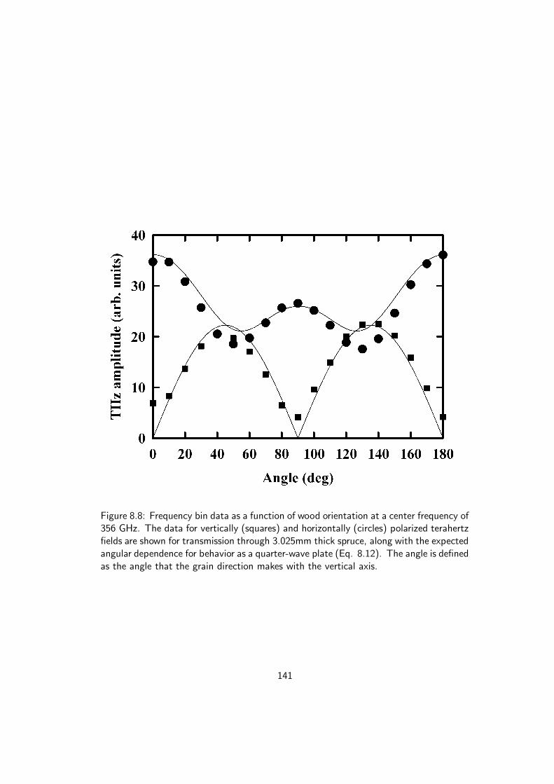
Figure 8.8: Frequency bin data as a function of wood orientation at a center frequency of356 GHz. The data for vertically (squares) and horizontally (circles) polarized terahertzfields are shown for transmission through 3.025mm thick spruce, along with the expectedangular dependence for behavior as a quarter-wave plate (Eq. 8.12). The angle is definedas the angle that the grain direction makes with the vertical axis.
141

Figure 8.9: Frequency bin data as a function of wood orientation at a center frequency of391 GHz. The data for vertically (squares) and horizontally (circles) polarized terahertzfields are shown for transmission through 3.025mm thick spruce, along with the expectedangular dependence for behavior as a quarter-wave plate (Eq. 8.12). The angle is definedas the angle that the grain direction makes with the vertical axis.
142

Figure 8.10: Frequency bin data as a function of wood orientation at a center frequencyof 711 GHz. The data for vertically (squares) and horizontally (circles) polarized tera-hertz fields are shown for transmission through 3.025mm thick spruce, along with theexpected angular dependence for behavior as a half-wave plate (Eq. 8.12). The angleis defined as the angle that the grain direction makes with the vertical axis.
143

Figure 8.11: Operating point for mapping time delay of terahertz radiation to bire-fringence data. The figure shows a typical terahertz time-domain waveform, and thelocation of the operating point is shown in the inset. The lock-in amplifier signal iszeroed at the operating point, and the lens paper sample is rotated about its surfacenormal to map time-delay to amplitude information.
144

Figure 8.12: Lock-in amplifier signal as a function of orientation for transmission ofterahertz radiation through 27 pieces of aligned lens paper. The lens paper oriented withfiber alignment vertical corresponds to zero degrees in the figure. The input terahertzfield is polarized horizontally. The measured signal corresponds to mapping time delayto birefringence (see text for details).
145

Figure 8.13: Terahertz signal as function of time delay for reference (solid), transmissionthrough 21 µm thick single piece of lens paper with terahertz polarization perpendicular(long dashed) and parallel (short dashed) to the fiber orientation on an expanded scale.All three time-domain scans are shown in the inset, and are virtually indistinguishableon that scale. nf and ns represent the fast and slow axes, respectively.
146

Figure 8.14: Index of refraction of a 21 µm thick piece of lens paper obtained withterahertz polarization perpendicular (long dashed) and parallel (solid) to the fiber ori-entation. nf and ns represent the fast and slow axes, respectively.
147

Figure 8.15: Optical image of the 2 mm thick piece of fir wood used for a lineartransmission terahertz map (see text for details).
Figure 8.16: Terahertz transmission measurements as function of linear distance along apiece of fir. The top picture shows an optical image of the lateral scan, while the bottomfigure plots the peak transmitted terahertz field amplitude as a function of displacement.
148

Figure 8.17: Optical picture of 2.2 mm thick fir (left) and terahertz transmission imageof the same sample (right). Note that dark rings on left appear as dark rings on thefigure in the right, as the higher porosity and larger density maps to higher terahertzattenuation. The scale on the upper left corresponds to the signal strength scale for theTHz image.
149

Chapter 9
Conclusion and future work
9.1 Conclusions
Terahertz emission has been studied at high excitation fluences from GaAs, InAs andInP emitters in order to optimize their performance as sources of far-infrared radiationfor industrial applications.
The emission of terahertz radiation from InAs surfaces was examined as a func-tion of excitation fluence, and directly compared to the emission from a large-aperturephotoconductive switch. It was found that the large aperture-photoconductive switchdemonstrated a larger conversion efficiency. At an applied bias field of 1.6 kV / cm, themaximum conversion efficiency obtained with the large-aperture photoconductive switchwas 1.9 × 10⁻⁵ in comparison to an unbiased (100) InAs surface, for which a measuredmaximum conversion efficiency of 2.1 × 10⁻⁶ was obtained. A reduced dependence ofthe radiated terahertz field on an applied magnetic field at high excitation fluences wasobserved, which indicates at most an enhancement of 3 times in performance of theInAs emitter could be expected with the application of a large 2 T magnetic field.
The emission mechanism from InAs surfaces at high excitation fluences was exam-ined in detail. Pump polarization dependencies of terahertz radiation from the (100)crystal face of InAs demonstrated that the emission was dominated by a process otherthan bulk optical rectification or photo-carrier-related emission, which only contributeat levels of 13 % and 20 %, respectively. Complete calculations of bulk optical rectifica-tion and surface electric-field induced optical rectification were presented and comparedto experimental results for terahertz emission and optical second harmonic generationfrom (100), (110) and (111) crystal faces of InAs. It was determined that the domi-nant emission mechanism for terahertz radiation from InAs surfaces is consistent withsurface electric-field induced optical rectification, while the second-harmonic emission isconsistent with bulk second-harmonic generation. Comparison of terahertz emission andoptical second-harmonic emission from the InAs crystal faces revealed that a likely expla-nation for the dominant contribution to the terahertz radiation from surface electric-field
150

induced optical rectification is the large free-carrier contribution to the third-order sus-ceptibility in InAs which scales with the inverse of the output frequency.
In order to try to enhance the conversion efficiency from semiconductor surfaceemitters, structuring of the surfaces was investigated. It was demonstrated that opticalnonlinear interactions at semiconductor surfaces could be enhanced with the introductionof porosity. Porous samples of InP were shown to exhibit increased optical rectification,as well as second-harmonic generation, in comparison to bulk samples of InP, with outputintensities on the order of 20 to 100 times those from unstructured surfaces, dependingon the radiation process and polarization geometry used.
A system was constructed for spectroscopy measurements, employing a semi-largeaperture photoconductive switch and characterized in detail. It was found that theoverall conversion efficiency was approximately 2×10⁻⁷, limited by the magnitude of theapplied bias field and collection angle losses within the system, which could potentiallybe improved with the addition of a silicon collimating lens and an improved amplifierdesign for the bias field. The large signal-to-noise ratios and short acquisition timesthat are obtained using this set-up are a substantial improvement over the other sourcesstudied in this thesis.
The application of pulsed terahertz radiation to wood and wood products was investi-gated. The terahertz properties of wood were first studied in detail. It was demonstratedthat several wood species measured exhibit both diattenuation and birefringence. Themagnitude of the birefringence was in the range of 0.06 to 0.13 depending on the woodspecies measured. This birefringence could also be used to determine fiber alignmentin wood products and the sensitivity of this system was demonstrated by measuring thebirefringence of a single piece of lens paper (20 µm thick) in less than a second. Thedependence of terahertz transmission on the presence of early and latewood was alsodemonstrated and used to map out the grain pattern in a piece of wood.
9.2 Future Work
There are several questions that have been raised throughout this thesis, which requiresubstantially more work to answer. These questions will be highlighted here.
In the data presented, the two processes of surface electric-field induced optical recti-fication and surface optical rectification cannot be distinguished from the measurementsmade in this thesis. One possible way to proceed with separating these two contribu-tions would be to perform a systematic investigation of the terahertz emission from cleanoxide-free InAs surfaces, and from samples with different doping concentrations. Thedoping concentration would affect the surface electric field, while having little effect onthe pure surface nonlinear optical response.
It has been demonstrated that the introduction of porosity could enhance the bulknonlinear optical response to the radiated terahertz field from InP surfaces. The tentativemechanism responsible for the increase was attributed to local-field enhancement within
151

the porous network. However, further measurements will be required to clarify thisdependence and resolve whether other enhancement mechanisms are also involved.
As surface electric-field induced optical rectification is also a nonlinear optical pro-cess, it stands to reason that local-field enhancement would work to improve the con-version efficiency for terahertz radiation from InAs surfaces at high excitation fluence.In order to demonstrate whether or not this is a fact, high quality porous InAs samplesare required which are not currently available. With such high-quality samples, it maybe possible to generate terahertz fields from InAs surfaces with conversion efficiencies30 to 100 times higher than the present solid surfaces making a large-aperture geometrycompetitive with large-aperture photoconductive switches. The benefit that this wouldhave is that external bias fields and extensive cooling would not be required. Furtherwork on both the enhancement mechanism for nonlinear optical interactions within theporous network as well as manufacturing of high-quality porous InAs would be requiredfor this.
It was found that wood exhibits both birefringence and diattenuation in the terahertzfrequency range. These properties are intrinsically related to the structural propertiesof wood. For example, the cell diameter and wall thickness likely contribute to thediattenuation. However, absorption within the wood due to water is expected to besignificant due to the large absorption coefficient of water in the far-infrared. Therefore,it would be desirable to quantify the absorption of terahertz radiation by water withinwood products. This may also be useful, for example, as a tool for measuring thewater content for wood. A further refinement could be to investigate THz probing in areflection geometry from wood such that thin samples would not be required and sucha system could easily be adapted for use in industry.
152

Bibliography
[1] P. D. Coleman, “Reminiscences on selected millennium highlights in the questfor tunable terahertz-submillimeter wave oscillators,” IEEE J. Sel. Top. Quant.
Electron., vol. 6, pp. 1000–1007, 2000.
[2] D. H. Auston, K. P. Cheung, and P. R. Smith, “Picosecond photoconductinghertzian dipoles,” Appl. Phys. Lett., vol. 45, pp. 284–286, 1984.
[3] M. van Exter and D. Grischkowsky, “Characterization of an optoelectronic tera-hertz beam system,” IEEE Trans. Microwave Theory Tech., vol. 38, pp. 1684–1691, 1990.
[4] G. Zhao, R. N. Schouten, N. van der Valk, W. T. Wenckebach, and P. C. M.Planken, “Design and performance of THz emission and detection setup based ona semi-insulating GaAs emitter,” Rev. Sci. Inst., vol. 73, pp. 1715–1719, 2002.
[5] B. B. Hu and M. C. Nuss, “Imaging with terahertz waves,” Opt. Lett., vol. 20,pp. 1716–1718, 1995.
[6] D. Mittleman, R. Jacobsen, and M. Nuss, “T-ray imaging,” IEEE J. Sel. Top.
Quant. Electron., vol. 2, pp. 679–692, 1996.
[7] B. Ferguson, S. Wang, D. Gray, D. Abbot, and X. C. Zhang, “T-ray computedtomography,” Opt. Lett., vol. 27, pp. 1312–1314, 2002.
[8] K. McClatchey, M. T. Reiten, and R. A. Cheville, “Time-resolved synthetic aper-ture terahertz impulse imaging,” Appl. Phys. Lett., vol. 79, pp. 4485–4487, 2001.
[9] T. D. Dorney, W. W. Symes, R. G. Baraniuk, and D. M. Mittleman, “Terahertzmultistatic reflection imaging,” J. Opt. Soc. Am. A, vol. 19, pp. 1432–1442, 2002.
[10] Z. Jiang and X. C. Zhang, “Terahertz imaging via electrooptic effect,” IEEE Trans.
Microwave Theory Tech., vol. 47, pp. 2644–2650, 1999.
[11] A. Nahata, J. T. Yardley, and T. F. Heinz, “Two-dimensional imaging ofcontinuous-wave terahertz radiation using electro-optic detection,” Appl. Phys.
Lett., vol. 81, pp. 963–965, 2002.
153

[12] J. E. Bjarnason, T. L. J. Chan, A. W. M. Lee, M. A. Celis, and E. R. Brown,“Millimeter-wave, terahertz and mid-infrared transmission through common cloth-ing,” Appl. Phys. Lett., vol. 85, pp. 519–521, 2004.
[13] H. Zhong, N. Karpowicz, J. Partridge, X. Xie, J. Xu, and X. C. Zhang, “Terahertzwave imaging for landmine detection,” in Proc. SPIE, vol. 5411, pp. 33–44, 2004.
[14] V. P. Wallace, R. M. Woodward, A. J. Fitzgerald, E. Pickwell, R. J. Pye, andD. A. Arnone, “Terahertz pulsed imaging of cancers,” in Proc. SPIE, vol. 4949,pp. 353–359, 2003.
[15] D. Crawley, C. Longbottom, V. P. Wallace, B. Cole, D. Arnone, and M. Pepper,“Three-dimensional teraherz pulse imagaging of dental tissue,” in Proc. SPIE,vol. 4633, pp. 84–89, 2002.
[16] M. van Exter, C. Fattinger, and D. Grischkowsky, “Terahertz time-domain spec-troscopy of water vapor,” Opt. Lett., vol. 14, pp. 1128–1130, 1989.
[17] L. Thrane, R. H. Jacobsen, P. U. Hepsen, and S. R. Keiding, “THz reflectionspectroscopy of liquid water,” Chem. Phys. Lett., vol. 240, pp. 330–333, 1995.
[18] R. A. Cheville and D. Grischkowsky, “Observation of pure rotational absorptionspectra in the ν2 band of hot H2O in flames,” Opt. Lett., vol. 23, pp. 531–533,1996.
[19] J. Zhang and D. Grischkowsky, “Waveguide terahertz time-domain spectroscopyof nanometer water layers,” Opt. Lett., vol. 29, pp. 1617–1619, 2004.
[20] J. Zhang and D. Grischkowsky, “Terahertz time-domain spectroscopy of submono-layer water adsorption in hydrophilic silica aerogel,” Opt. Lett., vol. 29, pp. 1031–1033, 2004.
[21] D. M. Mittleman, R. H. Jacobsen, R. Neelamani, R. G. Baraniuk, and M. C. Nuss,“Gas sensing using terahertz time-domain spectroscopy,” Appl. Phys. B, vol. 67,pp. 379–390, 1998.
[22] M. Walther, S. Fischer, M. Shcall, H. Helm, and P. U. Jepsen, “Far-infraredvibrational spectra all trans, 9-cis and 13-cis retinal measured by THz time-domainspectroscopy,” Chem. Phys. Lett., vol. 332, pp. 389–396, 2000.
[23] A. G. Markelz, A. Roitberg, and E. J. Heilweil, “Pulsed terahertz spectroscopyof DNA, bovine serum albumin and collagen between 0.1 and 2.0 THz,” Chem.
Phys. Lett., vol. 320, pp. 42–48, 2000.
[24] K. Kawase, Y. Ogawa, Y. Watanabe, and H. Inoue, “Non-destructive tera-hertz imaging of illicit drugs using spectral fingerprints,” Opt. Express, vol. 11,pp. 2549–2554, 2003.
154

[25] D. Grischkowsky, S. Keiding, M. van Exter, and C. Fattinger, “Far-infrared time-domain spectroscopy with terahertz beams of dielectrics and semiconductors,” J.
Opt. Soc. Am. B, vol. 7, pp. 2006–2015, 1990.
[26] M. C. Beard, G. M. Turner, and C. A. Schmuttenmaer, “Subpicosecond carrierdynamics in low-temperature grown GaAs as measured by time-resolved terahertzspectroscopy,” Phys. Rev. Lett., vol. 86, pp. 340–343, 2001.
[27] F. A. Hegmann, R. R. Tywinski, K. P. H. Lui, J. E. Bullock, and J. E. Anthony,“Picosecond transient photoconductivity in functionalized pentacene molecularcrystals probed by terahertz spectroscopy,” Phys. Rev. Lett., vol. 89, pp. 2274031–2274034, 2002.
[28] E. Knoesel, M. Bonn, J. Shan, and T. F. Heinz, “Charge transport and carrierdynamics in liquids probed by THz time-domain spectroscopy,” Phys. Rev. Lett.,vol. 86, pp. 340–343, 2001.
[29] M. C. Kemp, P. F. Taday, B. E. Cole, J. A. Cluff, A. J. Fitzgerald, and W. R. Tribe,“Security applications of terahertz imaging,” in Proc. SPIE, vol. 5070, pp. 44–52,2003.
[30] G. C. Walker, E. Berry, N. N. Zinov’ev, A. J. Fitzgerald, R. E. Miles, M. Cham-berlain, and M. A. Smith, “Teraherz imaging and international safety guidelines,”in Proc. SPIE, vol. 4682, pp. 683–690, 2002.
[31] X.-C. Zhang and D. H. Auston, “Optoelectronic measurement of semiconductorsurfaces and interfaces with femtosecond optics,” J. Appl. Phys., vol. 71, pp. 326–338, 1992.
[32] B. B. Hu, X.-C. Zhang, D. H. Auston, and P. R. Smith, “Free-space radiationfrom electro-optic crystals,” Appl. Phys. Lett., vol. 56, pp. 506–508, 1990.
[33] L. Xu, X.-C. Zhang, and D. H. Auston, “Terahertz beam generation by fem-tosecond optical pulses in electro-optic materials,” Appl. Phys. Lett., vol. 61,pp. 1784–1786, 1992.
[34] N. Sarukura, H. Ohtake, S. Izumida, and Z. Liu, “High average-power THz radi-ation from femtosecond laser-irradiated InAs in a magnetic field and its ellipticalpolarization characteristics,” J. Appl. Phys., vol. 84, pp. 654–656, 1998.
[35] C. Weiss, R. Wallenstein, and R. Beigang, “Magnetic-field-enhanced generationof terahertz radiation in semiconductor surfaces,” Appl. Phys. Lett., vol. 77,pp. 4160–4162, 2000.
[36] J. Shan, C. Weiss, R. Wallenstein, R. Beigang, and T. F. Heinz, “Origin of mag-netic field enhancement in the generation of terahertz radiation from semiconduc-tor surfaces,” Opt. Lett., vol. 26, pp. 849–851, 2001.
155

[37] R. McLaughlin, A. Corchia, M. B. Johnston, Q. Chen, C. M. Ciesla, D. D. Arnone,G. A. C. Jones, E. H. linfield, A. G. Davies, and M. Pepper, “Enhanced coherentterahertz emission from indium arsenide in the presence of a magnetic field,” Appl.
Phys. Lett., vol. 76, pp. 2038–2040, 2000.
[38] J. N. Heyman, P. Neocleous, D. Hebert, P. A. Crowell, T. Mueller, and K. Unter-rainer, “Terahertz emission from GaAs and InAs in a magnetic field,” Phys. Rev.
B., vol. 64, pp. 0852021–0852027, 2001.
[39] M. Nakajima, M. Hangyo, M. Ohta, and H. Miyazaki, “Polarity reversal of tera-hertz waves radiated from semi-insulating InP surfaces induced by temperature,”Phys. Rev. B., vol. 67, pp. 195308–7, 2003.
[40] T. Dekorsy, H. Auer, H. J. Baker, H. G. Roskos, and H. Kurz, “THz electro-magnetic emission by coherent infrared-active phonons,” Phys. Rev. B., vol. 53,pp. 4005–4014, 1996.
[41] S. Chuang, S. Schmitt-Ring, B. Greene, P. Saeta, and A. Levi, “Optical rectifica-tion at semiconductor surfaces,” Phys. Rev. Lett., vol. 68, pp. 102–105, 1992.
[42] D. You, R. R. Jones, P. H. Bucksbaum, and D. R. Dykaar, “Coherent generationof far-infrared radiation from InP,” J. Opt. Soc. Am. B., vol. 11, pp. 486–491,1994.
[43] P. Saeta, B. Greene, and S. Chuang, “Short terahertz pulses from semiconductorsurfaces: The importance of bulk difference-frequency mixing,” Appl. Phys. Lett.,vol. 63, pp. 3482–3484, 1993.
[44] M. Nakajima, Y. Oda, and T. Suemoto, “Competing terahertz radiation mecha-nisms in semi-insulating InP at high-density excitation,” Appl. Phys. Lett., vol. 85,pp. 2694–2696, 2004.
[45] W. Lukosz, “Light emission by magnetic and electric dipoles close to a planedielectric interface. iii. radiation patterns of dipoles with arbitrary orientation,” J.
Opt. Soc. Am., vol. 69, pp. 1495–1503, 1979.
[46] H. K. Yang, P. L. Richards, and Y. R. Shen, “A wideband coherent terahertzspectroscopy system using optical rectification and electro-optic sampling,” Appl.
Phys. Lett., vol. 19, pp. 320–323, 1971.
[47] T. A. Germer, K. W. Kolasinski, J. C. Stephenson, and L. J. Richter, “Depletion-electric-field-induced second-harmonic generation near oxidized GaAs (001) sur-faces,” Phys. Rev. B, vol. 55, pp. 10694–10706, 1997.
[48] D. Dragoman and M. Dragoman, “Terahertz fields and applications,” Progr.
Quant. Electr., vol. 28, pp. 1–66, 2004.
156

[49] P. C. M. Planken, H.-K. Nienhuys, H. J. Bakker, and T. Wenckebach, “Measure-ment and calculation of the orientation dependence of terahertz pulse detectionin ZnTe,” J. Opt. Soc. Am. B., vol. 18, pp. 313–317, 2001.
[50] E. Gerecht, C. F. Musante, Y. Zhuang, K. S. Yngvesson, T. Goyette, J. C. Dick-inson, J. Waldman, P. A. Yagoubov, G. N. Goltsman, B. M. Voronav, and E. M.Gershenzon, “NbN hot electron bolometric mixers - a new technology for low-noiseTHz recievers,” IEEE Trans. Microwave Theory Tech., vol. 47, pp. 2519–2527,1999.
[51] P. Y. Han, M. Tani, M. Usami, S. Kono, R. Kersting, and X. C. Zhang, “A directcomparison between terahertz time-domain spectroscopy and far-infrared fouriertransform spectroscopy,” J. Appl. Phys., vol. 89, pp. 2357–2359, 2001.
[52] S.-G. Park, M. R. Melloch, and A. M. Weiner, “Comparison of terahertz wave-forms measured by electro-optic and photoconductive sampling,” Appl. Phys.
Lett., vol. 73, pp. 3184–3186, 1998.
[53] Y. Cai, I. Brener, J. Lopata, J. Wynn, L. Pfeiffer, J. B. Stark, Q. Wu, X. C. Zhang,and J. F. Federici, “Coherent terahertz radiation detection: Direct comparisonbetween free-space electro-optic sampling and antenna detection,” Appl. Phys.
Lett., vol. 73, pp. 444–446, 1998.
[54] Z. Jiang and X. C. Zhang, “Electro-optic measurement of THz field pulses witha chirped optical beam,” Appl. Phys. Lett., vol. 72, pp. 1945–1947, 1998.
[55] J. Shan, A. S. Weling, E. Knoesel, L. Bartels, M. Bonn, A. Nahata, G. A. Reider,and T. F. Heinz, “Single-shot measurement of terahertz electromagnetic pulsesby use of electro-optic sampling,” Opt. Lett., vol. 25, pp. 426–428, 2000.
[56] Q. Wu and X. C. Zhang, “Free-space electro-optics sampling of mid-infraredpulses,” Appl. Phys. Lett., vol. 71, pp. 1285–1287, 1997.
[57] A. Leitenstorfer, S. Hunsche, J. Shah, M. C. Nuss, and W. H. Knox, “Detectorsand sources for ultrabroadband electro-optic sampling: Experiment and theory,”Appl. Phys. Lett., vol. 74, pp. 1516–1518, 1999.
[58] Q. Wu and X. C. Zhang, “Design and characterization of traveling-wave electroop-tic terahertz sensors,” IEEE J. Sel. Top. Quantum Electron., vol. 2, pp. 693–700,1996.
[59] F. L. Pedrotti and L. S. Pedrotti, Introduction to Optics. New Jersey: PrenticeHall, 2nd ed., 1993.
[60] R. W. Boyd, Nonlinear Optics. San Diego: Academic Press, 2nd ed., 2003.
157

[61] M. Abarkan, J. P. Salvestrini, M. D. Fontana, and M. Aillerie, “Frequency andwavelength dependences of electro-optic coefficients in inorganic crystals,” Appl.
Phys. B, vol. 76, pp. 765–769, 2003.
[62] E. H. Turner, “High-frequency electro-optic coefficients of lithium niobate,” Appl.
Phys. Lett., vol. 8, pp. 303–304, 1966.
[63] P. U. Jepsen, C. Winnewisser, M. Schall, V. Schyja, S. R. Keiding, and H. Helm,“Detection of THz pulses by phase retardation in lithium tantalate,” Phys. Rev.
B, vol. 53, pp. R3052–R3054, 1996.
[64] C. Winnewisser, P. U. Jepsen, M. Schall, V. Schyja, and H. Helm, “Electro-opticdetection of THz radiation in LiTaO3, LiNbO3 and ZnTe,” Appl. Phys. Lett.,vol. 70, pp. 3069–3071, 1997.
[65] A. Nahata, A. S. Weling, and T. F. Heinz, “A wideband coherent terahertzspectroscopy system using optical rectification and electro-optic sampling,” Appl.
Phys. Lett., vol. 69, pp. 2321–2323, 1996.
[66] G. D. Boyd, W. L. Bond, and H. L. Carter, “Refractive index as a function oftemperature in LiNb03,” J. Appl. Phys., vol. 38, pp. 1941–1943, 1967.
[67] M. Schall, H. Helm, and S. R. Keiding, “Far infrared properties of electro-opticcrystals measured by THz time-domain spectroscopy,” Int. J. of Infrared and
Millimeter Waves, vol. 20, pp. 595–604, 1999.
[68] T. Hattori, K. Tukamoto, and H. Nakatsuka, “Time-resolved study of intenseterahertz pulses generated by a large-aperture photoconductive antenna,” Jpn. J.
Appl. Phys., vol. 40, pp. 4907–4912, 2001.
[69] Q. Wu and X. C. Zhang, “7 terahertz broadband GaP electro-optic sensor,” Appl.
Phys. Lett., vol. 70, pp. 1784–1786, 1997.
[70] A. Nahata, J. T. Yardley, and T. F. Heinz, “Free-space electro-optic detection ofcontinuous-wave terahertz radiation,” Appl. Phys. Lett., vol. 75, pp. 2524–2526,1999.
[71] M. Reid and R. Fedosejevs, “Quantitative comparison of THz emission from (100)InAs surfaces and GaAs large-aperture photoconductive switch at high fluences,”Appl. Opt., vol. 44, pp. 149–153, 2004.
[72] J. T. Darrow, X.-C. Zhang, and D. H. Auston, “Saturation properties oflarge-aperture photoconducting antennas,” IEEE J. Quantum Electron., vol. 28,pp. 1607–1616, 1992.
158

[73] D. You, R. R. Jones, P. H. Bucksbaum, and D. R. Dykaar, “”generation ofhigh-power sub-single-cycle 500-fs electromagnetic pulses”,” Opt. Lett., vol. 18,pp. 290–292, 1993.
[74] T. Loffler and H. G. Roskos, “Gas-pressure dependence of terahertz-pulse genera-tion in a laser-generated nitrogen plasma,” J. Appl. Phys., vol. 91, pp. 2611–2614,2002.
[75] A. Gurtler, C. Winnewisser, H. Helm, and P. U. Jepsen, “Terahertz propagationin the near field and far field,” J. Opt. Soc. Am. A., vol. 17, pp. 74–83, 2000.
[76] D. You and P. H. Bucksbaum, “Propagation of half-cycle far infrared pulses,” J.
Opt. Soc. Am. B., vol. 14, pp. 1651–1655, 1997.
[77] E. Budiarto, N.-W. Pu, S. Jeong, and J. Bokor, “Near-field propagation of ter-ahertz pulses from a large-aperture antenna,” Opt. Lett., vol. 23, pp. 213–215,1998.
[78] G. Rodriguez and A. J. Taylor, “Screening of the bias field in terahertz generationfrom photoconductors,” Opt. Lett., vol. 21, pp. 1046–1048, 1996.
[79] H. Takahashi, Y. Suzuki, A. Quema, M. Sakai, T. Yano, S. Ono, N. Sarukura,M. Hosomizu, T. Tsukamoto, G. Nishijima, and K. Watanabe, “Magnetic-field-induced enhancement of THz-radiation power from femtosecond-laser-irradiatedInAs up to 27T,” Jpn. J. Appl. Phys., vol. 42, pp. L532–L534, 2003.
[80] H. Takahashi, Y. Suzuki, M. Sakai, S. Ono, N. Sarukura, T. Sugiura, T. Hirosumi,and M. Yoshida, “Significant enhancement of terahertz radiation from InSb by useof a compact fiber laser and an external magnetic field,” Appl. Phys. Lett., vol. 82,pp. 2005–2007, 2003.
[81] M. Hangyo, M. Migita, and K. Nakayama, “Magnetic field and temperature de-pendence of terahertz radiation from InAs surfaces excited by femtosecond laserpulses,” J. Appl. Phys., vol. 90, pp. 3409–3412, 2001.
[82] H. Takahashi, A. Quema, R. Yoshioka, S. Ono, and N. Sarukura, “Excitationfluence dependence of terahertz radiation mechanism from femtosecond-laser-irradiated InAs under magnetic field,” Appl. Phys. Lett., vol. 82, pp. 1068–1070,2003.
[83] T. Hattori, R. Rungsawang, K. Ohta, and K. Tukamoto, “Gaussian beam analysisof temporal waveform of focused terahertz pulses,” Jpn. J. Appl. Phys., vol. 41,pp. 5198–5204, 2002.
[84] M. Reid and R. Fedosejevs, “Terahertz emission from (100) InAs surfaces at highexcitation fluence,” Appl. Phys. Lett., vol. 86, pp. 011904–011906, 2005.
159

[85] M. Reid and R. Fedosejevs, “Terahertz emission from surface optical rectificationin n-InAs,” in Proc. SPIE, vol. 5577, pp. 659–669, 2004.
[86] M. B. Johnston, D. M. Whittaker, A. Corchia, A. G. Davies, and E. H. Linfield,“Simulation of terahertz generation at semiconductor surfaces,” Phys. Rev. B.,vol. 65, pp. 1653011–1653018, 2002.
[87] B. I. Greene, P. N. Saeta, D. R. Dykaar, S. Schmitt-Rink, and S. L. Chuang,“Far-infrared light generation at semiconductor surfaces and its spectroscopic ap-plications,” IEEE J. Quantum. Electron., vol. 28, pp. 2302–2311, 1992.
[88] S. Howells and L. Schlie, “Temperature dependence of terahertz pulses producedby difference-frequency mixing in InSb,” Appl. Phys. Lett., vol. 67, pp. 3688–3690,1995.
[89] S. Kono, P. Gu, M. Tani, and K. Sakai, “Temperature dependence of terahertzradiation from n-type InSb and n-type InAs surfaces,” Appl. Phys. B, vol. 71,pp. 901–904, 2000.
[90] P. Gu, M. Tani, S. Kono, K. Sakai, and X.-C. Zhang, “Study of terahertz radiationfrom InAs and InSb,” J. Appl. Phys., vol. 91, pp. 5533–5537, 2002.
[91] J. Sipe, D. Moss, and H. van Driel, “Phenomenological theory of optical second-and third-harmonic generation from cubic centrosymmetric crystals,” Phys. Rev.
B., vol. 35, pp. 1129–1140, 1987.
[92] W. Hubner, K. Bennemann, and K. Bohmer, “Theory for the nonlinear opticalresponse of transition metals: Polarization dependence as a fingerprint of theelectronic structure at suraces and interfaces,” Phys. Rev. B, vol. 50, pp. 17597–17605, 1994.
[93] T. Stehlin, M. Feller, P. Guyot-Sionnest, and Y. Shen, “Optical second-harmonicgeneration as a surface probe for noncentrosymmetric media,” Opt. Lett., vol. 13,pp. 389–391, 1988.
[94] N. Bloembergen, “Surface nonlinear optics: a historical overview,” Appl. Phys.
B, vol. 68, pp. 289–293, 1999.
[95] J. F. McGilp, “A review of optical second-harmonic and sum-frequency generationat surfaces and interfaces,” J. Phys. D, vol. 29, pp. 1812–1821, 1996.
[96] Y. R. Shen, “Surface contribution versus bulk contribution in surface nonlinearoptical spectroscopy,” Appl. Phys. B, vol. 68, pp. 295–300, 1999.
[97] S. Adachi, Optical Constants of Crystalline and Amorphous Semiconductors.Boston: Kluwer Academic Publishers, 1st ed., 1999.
160

[98] P. N. Butcher and D. Cotter, The elements of Nonlinear Optics. Cambridge:Cambridge University Press, 1st ed., 1990.
[99] R. Adomavicius, A. Urbanowicz, G. Molis, A. Krotkus, and E. Satkovskis, “Ter-ahertz emission from p-InAs due to the instantaneous polarization,” Appl. Phys.
Lett., vol. 85, pp. 2463–2465, 2004.
[100] S. Buchner, L. Y. Ching, and E. Burstein, “Raman scattering at the (111) and(111) surfaces of n- and p-InAs,” Phys. Rev. B, vol. 14, pp. 4459–4462, 1976.
[101] W. Y. Ching and M. Z. Huang, “Calculation of optical excitations in cubic semi-conductors. III. third-harmonic generation,” Phys. Rev. B, vol. 47, pp. 9479–9491,1993.
[102] J. J. Wynne, “Optical third-order mixing in GaAs, Ge, Si, and InAs,” Phys. Rev.,vol. 178, pp. 1295–1303, 1969.
[103] S. S. Jha and N. Bloembergen, “Nonlinear optical susceptibilities in group-IV andIII-V semiconductors,” Phys. Rev., vol. 171, pp. 891–898, 1968.
[104] A. Mayer and F. Keilmann, “Far-infrared nonlinear optics II. χ(3) contributionsfrom the dynamics of free cariers in semiconductors,” Phys. Rev. B, vol. 33,pp. 6962–6968, 1986.
[105] M. Reid, I. V. Cravetchi, R. Fedosejevs, I. M. Tiginyanu, and L. Sirbu, “Enhancedterahertz emission from porous InP (111) membranes,” Appl. Phys. Lett., vol. 86,pp. 021904–1–021904–3, 2005.
[106] M. Reid, I. V. Cravetchi, R. Fedosejevs, I. M. Tiginyanu, L. Sirbu, and R. W. Boyd,“Enhanced nonlinear optical response of InP (100) membranes,” Phys. Rev. B,vol. 71, pp. 081306R–1–081306R–4, 2005.
[107] M. Reid, I. V. Cravetchi, R. Fedosejevs, I. M. Tiginyanu, L. Sirbu, and R. W. Boyd,“Enhanced terahertz emission from porous InP,” in Optical Terahertz Science and
Technology Topical Meeting on CD-ROM, p. WA4, 2005.
[108] I. M. Tiginyanu, I. V. Kravetsky, S. Langa, G. Marowsky, J. Monecke, and H. Foll,“Porous III-V compounds as nonlinear optical materials,” Phys. Stat. Sol. A,vol. 197, pp. 549–555, 2003.
[109] S. Langa, J. Carstensen, M. Christophersen, H. Foll, and I. Tiginyanu, “Observa-tion of crossing pores in anodically etched n-GaAs,” Appl. Phys. Lett., vol. 78,pp. 1074–1076, 2001.
161

[110] V. A. Mel’nikov, L. A. Golovan, S. O. Konorov, D. A. Muzychenko, A. B. Fedotov,A. M. Zheltikov, V. Y. Timoshenko, and P. K. Kashkarov, “Second-harmonic gen-eration in strongly scattering porous gallium phosphide,” Appl. Phys. B, vol. 79,pp. 225–228, 2004.
[111] L. A. Golovan, V. A. Mel’nikov, S. O. Konorov, A. B. Fedotov, S. A. Gavrilov,A. M. Zheltikov, P. K. Kashkarov, V. Y. Timoshenko, G. I. Petrov, L. Li, andV. V. Yakovlev, “Efficient second-harmonic generation by scattering from porousgalllium phosphide,” JETP Lett., vol. 78, pp. 193–197, 2003.
[112] P. U. Jepsen, R. H. Jacobsen, and S. R. Keiding, “Generation and detectionof terahertz pulses from biased semiconductor antennas,” J. Opts. Soc. Am. B,vol. 13, pp. 2424–2436, 1996.
[113] G. Zhao, R. N. Schouten, N. van der Valk, W. T. Wenckebach, and P. C. M.Planken, “A terahertz system using semi-large emitters: noise and performancecharacteristics,” Phys. Med. Biol., vol. 47, pp. 3609–3704, 2002.
[114] M. R. Stone, M. Naftaly, R. E. Miles, J. R. Fletcher, and D. P. Steenson, “Electri-cal and radiation characteristics of semilarge photoconductive terahertz emitters,”IEEE Trans. Microwave Theory Tech., vol. 52, pp. 2420–2429, 2004.
[115] S. Hadjiloucas, L. S. Karatzas, and J. W. Bowen, “Measurements of leaf watercontent using terahertz radiation,” IEEE Trans. Microwave Theory Tech., vol. 47,pp. 142–149, 1999.
[116] M. Koch, S. Hunsche, P. Schaucher, M. C. Nuss, J. Feldmann, and J. Fromm,“THz-imaging: a new method for density mapping of wood,” Wood Sci. Technol.,vol. 32, pp. 421–427, 1998.
[117] S. Hunsche and M. C. Nuss, “Terahertz ”T-ray” tomography,” in Proc. SPIE,vol. 3465, pp. 426–433, 1998.
[118] S. W. Smye, J. M. Chamberlain, A. J. Fitzgerald, and E. Berry, “The interactionbetween terahertz radiation and biological tissue,” Phys. Med. Biol., vol. 46,pp. R101–R112, 2001.
[119] L. Duvillaret, F. Garet, and J.-L. Coutaz, “A reliable method for extraction ofmaterial parameters in terahertz time-domain spectroscopy,” IEEE J. Sel. Top.
Quant. Electron., vol. 2, pp. 739–746, 1996.
[120] J. D. Jackson, Classical Electrodynamics. New York: John Wiley and Sons, Inc.,3rd ed., 1999.
[121] R. Boulay, B. Drouin, and R. Gagnon, “Method for measuring the fibre orientationanisotropy in a fibrous structure,” 1987.
162

[122] F. P. Kollmann and W. A. Cote, Principles of Wood Science and Technology I
Solid Wood. New York: Springer-Verlag, 1st ed., 1968.
[123] A. J. Stamm, Wood and Cellulose Science. New York: The Ronald Press Company,1st ed., 1964.
163

Appendix A
Appendix
A.1 Electro-optic detection in ZnTe
A.1.1 Derivation of relation 3.26
From Fig. 3.5 we can write:
tan(Ψ) =
√2C
−12B + 1
2
√B2 + 8C2
(A.1)
where
B = r41ETHzcos(θ)
C =r41ETHzsin(θ)√
2(A.2)
Inserting the definitions in Eq. A.2 into Eq. A.1, we obtain:
tan(Ψ) =2sin(θ)
−cos(θ) +√
cos2(θ) + 4sin2(θ)
=2tan(θ)
−1 +√
1 + 4tan2(θ)
⇒ tan(Ψ)√
1 + 4tan2(θ) = 2tan(θ) + tan(Ψ)
⇒ tan2(Ψ)(1 + 4tan2(θ)) = 4tan2(θ) + tan2(Ψ) + 4tan(θ)tan(Ψ)
⇒ 0 = 4tan2(θ)(1 − tan2(Ψ)) + 4tan(θ)tan(Ψ)
⇒ − tan(Ψ)
1 − tan2(Ψ)= tan(θ) (A.3)
164

Using the trigonometric identity:
tan(2x) =2tan(x)
1 − tan2(x)(A.4)
in Eq. A.3 we obtain the desired result:
tan(2Ψ) = −2tan(θ) (A.5)
A.1.2 Derivation of Eq. 3.35
The first derivation is as follows:
sin(2 [φ − Ψ]) = 2sin(φ − Ψ)cos(φ − Ψ)
= 2 (sin(φ)cos(Ψ) − cos(φ)sin(Ψ)) (cos(φ)cos(Ψ) + sin(φ)sin(Ψ))
= 2sin(φ)cos(φ)cos2(Ψ) − 2cos2(φ)cos(Ψ)sin(Ψ)
+ 2sin2(φ)cos(Ψ)sin(Ψ) − 2sin(φ)cos(φ)sin2(Ψ)
= 2([
cos2(Ψ) − sin2(Ψ)]
sin(φ)cos(φ) + sin(Ψ)cos(Ψ)[
sin2(φ) − cos2(φ)])
= 2
(
cos(2Ψ)1
2sin(2φ) − 1
2cos(2φ)sin(2Ψ)
)
= cos(2Ψ)sin(2φ) − cos(2φ)sin(2Ψ)
= cos(2Ψ) (sin(2φ) − tan(2Ψ)cos(2φ))
=(
cos2(Ψ) − sin2(Ψ))
(sin(2φ) − tan(2Ψ)cos(2φ)) (A.6)
The second identity is derived as follows:let
lhs ≡ sin(θ)
(
1 + tan2(Ψ)
tan(Ψ)
)
sin(2(φ − Ψ)) (A.7)
then
lhs = sin(θ)
(
1 + tan2(Ψ)
tan(Ψ)
)
(
cos2(Ψ) − sin2(Ψ))
(sin(2φ) − tan(2Ψ)cos(2φ))
(A.8)where the identity derived in Eq. A.6 has been used. We can then reduce as follows:
165

lhs = sin(θ)
(
1 + tan2(Ψ)
tan(Ψ)
)
(
cos2(Ψ) − sin2(Ψ))
(sin(2φ) − tan(2Ψ)cos(2φ))
= sin(θ)
(
cos4(Ψ) − sin4(Ψ)
cos(Ψ)sin(Ψ)
)
(sin(2φ) − tan(2Ψ)cos(2φ))
= 2sin(θ)
(
cos(2Ψ)
sin(2Ψ)
)
(sin(2φ) + 2tan(θ)cos(2φ)) (A.9)
where the relation in Eq. A.5 has been used. Continuing with Eq. A.9 we have:
lhs =
(
2sin(θ)
tan(2Ψ)
)
(sin(2φ) + 2tan(θ)cos(2φ))
= −cos(θ) (sin(2φ) + 2tan(θ)cos(2φ))
= − (cos(θ)sin(2φ) + 2sin(θ)cos(2φ)) (A.10)
This is the end of the derivation.
A.2 Calculation of the bulk electric-dipole contribution tononlinear susceptibility
In section 5.2.1, the independent elements of the susceptibility tensor were computedunder the application of a transformation. In this case, the transformation was a com-bination of a rotation to orient the z axis perpendicular to the crystal faces for each ofthe (100), (110) and (111) crystal faces, with a subsequent rotation about the surfacenormal by an amount φ. The total transformation matrix as given by Eq. 5.2 is writtenas: Rij, here, which is a 3 × 3 matrix. The new susceptibility elements in contractednotation are given by:
166

χxxx(φ)
d14= 6RxxRxyRxz
χyyy(φ)
d14= 6RyxRyyRyz
χzzz(φ)
d14= 6RzxRzyRzz
χxyy(φ)
d14= 2RxxRyyRyz + 2RxyRyxRyz + 2RxzRyxRyy
χyxx(φ)
d14= 2RyxRxyRxz + 2RyyRxxRxz + 2RyzRxyRxx
χxzz(φ)
d14= 2RxxRzyRzz + 2RxyRzxRzz + 2RxzRzyRzx
χzxx(φ)
d14= 2RzxRxyRxz + 2RzyRxxRxz + 2RzzRxyRxx
χyzz(φ)
d14= 2RyxRzyRzz + 2RyyRzxRzz + 2RyzRzyRzx
χzyy(φ)
d14= 2RzxRyyRyz + 2RzyRyzRyx + 2RzzRyyRyx
χxyz(φ)
d14= RxxRyyRzz + RxxRyzRzy + RxyRyzRzx
+ RxyRyxRzz + RxzRyxRyy + RxzRyyRzx
χyxz(φ)
d14= RyxRxyRzz + RyxRxzRzy + RyyRxzRzx
+ RyyRxxRzz + RyzRxxRzy + RyzRxyRzx
χzxy(φ)
d14= RzxRxyRyz + RzxRxzRyy + RzyRxzRyx
+ RzyRxxRyz + RzzRxxRyy + RzzRxyRyx
χxxz(φ)
d14= 2RxxRxyRzz + 2RxxRxzRzy + 2RxyRxzRzx
χxxy(φ)
d14= 2RxxRxyRyz + 2RxxRxzRyy + 2RxyRxzRyx
χyyz(φ)
d14= 2RyxRyyRzz + 2RyxRyzRzy + 2RyyRyzRzx
χzxz(φ)
d14= 2RzxRxyRzz + 2RzxRxzRzy + 2RzyRxxRzz
χzyz(φ)
d14= 2RzxRyyRzz + 2RzxRyzRzy + 2RzyRyxRzz
χyxy(φ)
d14= 2RyxRxyRyz + 2RyxRxzRyy + 2RyyRxxRyz (A.11)
167

It is important to note that this is for crystals of symmetry class 43m. However,this holds for an arbitrary rotation matrix, Rij .
Once the susceptibilites are found, the lattice polarization can be obtained. For thegeometry outlined in section 5.2.1, the lattice polarizations were calculated to be:
P (100)s = −4d14sin(2φ)t2pfsfcE
2p + 2d14cos(2φ)tstpfsEpEs
P(100)k = −2d14cos(2φ)t2pfsfcE
2p − 4d14sin(2φ)tstpfsEpEs
P (100)z = d14cos(2φ)t2sE
2s − d14cos(2φ)t2pf
2c E2
p − 2d14sin(2φ)tstpfcEpEs
P (110)s = 3d14cos(φ)sin2(φ)t2sE
2s +
d14
4(cos(φ) + 3cos(3φ))t2pf
2c E2
p
− d14cos(φ)t2pf2s E2
p − 2d14
4(sin(φ) − 3sin(3φ))tstpfcEpEs
P(110)k = −d14(sin(φ) − 3sin(3φ))t2sE
2s − 3d14cos
2(φ)sin(φ)t2pf2c E2
p
+ d14sin(φ)t2pf2s E2
p + 2d14
4(cos(φ) + 3cos(3φ))tstpfcEpEs
P (110)z = 2d14sin(φ)t2pfsfcE
2p − 2d14cos(φ)tstpfsEpEs
P (111)s =
√
2
3d14(t
2pf
2c E2
p − t2sE2s )sin(3φ) − 2d14√
3tstpfsEpEs
− 2
√
2
3d14tstpfcEpEscos(3φ)
P(111)k =
√
2
3d14(t
2pf
2c E2
p − t2sE2s )cos(3φ) − 2d14√
3tp2fsfcE
2p
+ 2
√
2
3d14tstpfcEpEssin(3φ)
P (111)z =
d14√3
(
2t2pf2s E2
p − t2pf2c E2
p − t2sE2s
)
(A.12)
A.3 Calculation of surface electric-field induced nonlinearity
Below, each independent element of the effective second order susceptibility tensor usedfor the calculation in section 5.3 is listed. The rotation matrix can be arbitrary, however,the elements are calculated only for a crystal with 43m symmetry.
168

χxxx = χ(3)iijj(RxxRxxRxyRzy + RxxRxxRxzRzz + RxyRxyRxxRzx)
+ χ(3)iijj(RxyRxyRxzRzz + RxzRxzRxxRzx + RxzRxzRxyRzy)
+ χ(3)ijij(RxxRxyRxxRzy + RxxRxzRxxRzz + RxyRxxRxyRzx)
+ χ(3)ijij(RxyRxzRxyRzz + RxzRxxRxzRzx + RxzRxyRxzRzy)
+ χ(3)ijji(RxxRxyRxyRzx + RxxRxzRxzRzx + RxyRxxRxxRzy)
+ χ(3)ijji(RxyRxzRxzRzy + RxzRxxRxxRzz + RxzRxyRxyRzz)
+ χ(3)iiii(RxxRxxRxxRzx + RxyRxyRxyRzy + RxzRxzRxzRzz) (A.13)
χyyy = χ(3)iijj(RyxRyxRyyRzy + RyxRyxRyzRzz + RyyRyyRyxRzx)
+ χ(3)iijj(RyyRyyRyzRzz + RyzRyzRyxRzx + RyzRyzRyyRzy)
+ χ(3)ijij(RyxRyyRyxRzy + RyxRyzRyxRzz + RyyRyxRyyRzx)
+ χ(3)ijij(RyyRyzRyyRzz + RyzRyxRyzRzx + RyzRyyRyzRzy)
+ χ(3)ijji(RyxRyyRyyRzx + RyxRyzRyzRzx + RyyRyxRyxRzy)
+ χ(3)ijji(RyyRyzRyzRzy + RyzRyxRyxRzz + RyzRyyRyyRzz)
+ χ(3)iiii(RyxRyxRyxRzx + RyyRyyRyyRzy + RyzRyzRyzRzz) (A.14)
χzzz = χ(3)iijj(RzxRzxRzyRzy + RzxRzxRzzRzz + RzyRzyRzxRzx)
+ χ(3)iijj(RzyRzyRzzRzz + RzzRzzRzxRzx + RzzRzzRzyRzy)
+ χ(3)ijij(RzxRzyRzxRzy + RzxRzzRzxRzz + RzyRzxRzyRzx)
+ χ(3)ijij(RzyRzzRzyRzz + RzzRzxRzzRzx + RzzRzyRzzRzy)
+ χ(3)ijji(RzxRzyRzyRzx + RzxRzzRzzRzx + RzyRzxRzxRzy)
+ χ(3)ijji(RzyRzzRzzRzy + RzzRzxRzxRzz + RzzRzyRzyRzz)
+ χ(3)iiii(RzxRzxRzxRzx + RzyRzyRzyRzy + RzzRzzRzzRzz) (A.15)
169

χxyy = χ(3)iijj(RxxRyxRyyRzy + RxxRyxRyzRzz + RxyRyyRyxRzx)
+ χ(3)iijj(RxyRyyRyzRzz + RxzRyzRyxRzx + RxzRyzRyyRzy)
+ χ(3)ijij(RxxRyyRyxRzy + RxxRyzRyxRzz + RxyRyxRyyRzx)
+ χ(3)ijij(RxyRyzRyyRzz + RxzRyxRyzRzx + RxzRyyRyzRzy)
+ χ(3)ijji(RxxRyyRyyRzx + RxxRyzRyzRzx + RxyRyxRyxRzy)
+ χ(3)ijji(RxyRyzRyzRzy + RxzRyxRyxRzz + RxzRyyRyyRzz)
+ χ(3)iiii(RxxRyxRyxRzx + RxyRyyRyyRzy + RxzRyzRyzRzz) (A.16)
χyxx = χ(3)iijj(RyxRxxRxyRzy + RyxRxxRxzRzz + RyyRxyRxxRzx)
+ χ(3)iijj(RyyRxyRxzRzz + RyzRxzRxxRzx + RyzRxzRxyRzy)
+ χ(3)ijij(RyxRxyRxxRzy + RyxRxzRxxRzz + RyyRxxRxyRzx)
+ χ(3)ijij(RyyRxzRxyRzz + RyzRxxRxzRzx + RyzRxyRxzRzy)
+ χ(3)ijji(RyxRxyRxyRzx + RyxRxzRxzRzx + RyyRxxRxxRzy)
+ χ(3)ijji(RyyRxzRxzRzy + RyzRxxRxxRzz + RyzRxyRxyRzz)
+ χ(3)iiii(RyxRxxRxxRzx + RyyRxyRxyRzy + RyzRxzRxzRzz) (A.17)
χxzz = χ(3)iijj(RxxRzxRzyRzy + RxxRzxRzzRzz + RxyRzyRzxRzx)
+ χ(3)iijj(RxyRzyRzzRzz + RxzRzzRzxRzx + RxzRzzRzyRzy)
+ χ(3)ijij(RxxRzyRzxRzy + RxxRzzRzxRzz + RxyRzxRzyRzx)
+ χ(3)ijij(RxyRzzRzyRzz + RxzRzxRzzRzx + RxzRzyRzzRzy)
+ χ(3)ijji(RxxRzyRzyRzx + RxxRzzRzzRzx + RxyRzxRzxRzy)
+ χ(3)ijji(RxyRzzRzzRzy + RxzRzxRzxRzz + RxzRzyRzyRzz)
+ χ(3)iiii(RxxRzxRzxRzx + RxyRzyRzyRzy + RxzRzzRzzRzz) (A.18)
170

χzxx = χ(3)iijj(RzxRxxRxyRzy + RzxRxxRxzRzz + RzyRxyRxxRzx)
+ χ(3)iijj(RzyRxyRxzRzz + RzzRxzRxxRzx + RzzRxzRxyRzy)
+ χ(3)ijij(RzxRxyRxxRzy + RzxRxzRxxRzz + RzyRxxRxyRzx)
+ χ(3)ijij(RzyRxzRxyRzz + RzzRxxRxzRzx + RzzRxyRxzRzy)
+ χ(3)ijji(RzxRxyRxyRzx + RzxRxzRxzRzx + RzyRxxRxxRzy)
+ χ(3)ijji(RzyRxzRxzRzy + RzzRxxRxxRzz + RzzRxyRxyRzz)
+ χ(3)iiii(RzxRxxRxxRzx + RzyRxyRxyRzy + RzzRxzRxzRzz) (A.19)
χyzz = χ(3)iijj(RyxRzxRzyRzy + RyxRzxRzzRzz + RyyRzyRzxRzx)
+ χ(3)iijj(RyyRzyRzzRzz + RyzRzzRzxRzx + RyzRzzRzyRzy)
+ χ(3)ijij(RyxRzyRzxRzy + RyxRzzRzxRzz + RyyRzxRzyRzx)
+ χ(3)ijij(RyyRzzRzyRzz + RyzRzxRzzRzx + RyzRzyRzzRzy)
+ χ(3)ijji(RyxRzyRzyRzx + RyxRzzRzzRzx + RyyRzxRzxRzy)
+ χ(3)ijji(RyyRzzRzzRzy + RyzRzxRzxRzz + RyzRzyRzyRzz)
+ χ(3)iiii(RyxRzxRzxRzx + RyyRzyRzyRzy + RyzRzzRzzRzz) (A.20)
χzyy = χ(3)iijj(RzxRyxRyyRzy + RzxRyxRyzRzz + RzyRyyRyxRzx)
+ χ(3)iijj(RzyRyyRyzRzz + RzzRyzRyxRzx + RzzRyzRyyRzy)
+ χ(3)ijij(RzxRyyRyxRzy + RzxRyzRyxRzz + RzyRyxRyyRzx)
+ χ(3)ijij(RzyRyzRyyRzz + RzzRyxRyzRzx + RzzRyyRyzRzy)
+ χ(3)ijji(RzxRyyRyyRzx + RzxRyzRyzRzx + RzyRyxRyxRzy)
+ chi(3)ijji(RzyRyzRyzRzy + RzzRyxRyxRzz + RzzRyyRyyRzz)
+ χ(3)iiii(RzxRyxRyxRzx + RzyRyyRyyRzy + RzzRyzRyzRzz) (A.21)
171

χxyz = χ(3)iijj(RxxRyxRzyRzy + RxxRyxRzzRzz + RxyRyyRzxRzx)
+ χ(3)iijj(RxyRyyRzzRzz + RxzRyzRzxRzx + RxzRyzRzyRzy)
+ χ(3)ijij(RxxRyyRzxRzy + RxxRyzRzxRzz + RxyRyxRzyRzx)
+ χ(3)ijij(RxyRyzRzyRzz + RxzRyxRzzRzx + RxzRyyRzzRzy)
+ χ(3)ijji(RxxRyyRzyRzx + RxxRyzRzzRzx + RxyRyxRzxRzy)
+ χ(3)ijji(RxyRyzRzzRzy + RxzRyxRzxRzz + RxzRyyRzyRzz)
+ χ(3)iiii(RxxRyxRzxRzx + RxyRyyRzyRzy + RxzRyzRzzRzz) (A.22)
χyxz = χ(3)iijj(RyxRxxRzyRzy + RyxRxxRzzRzz + RyyRxyRzxRzx)
+ χ(3)iijj(RyyRxyRzzRzz + RyzRxzRzxRzx + RyzRxzRzyRzy)
+ χ(3)ijij(RyxRxyRzxRzy + RyxRxzRzxRzz + RyyRxxRzyRzx)
+ χ(3)ijij(RyyRxzRzyRzz + RyzRxxRzzRzx + RyzRxyRzzRzy)
+ χ(3)ijji(RyxRxyRzyRzx + RyxRxzRzzRzx + RyyRxxRzxRzy)
+ χ(3)ijji(RyyRxzRzzRzy + RyzRxxRzxRzz + RyzRxyRzyRzz)
+ χ(3)iiii(RyxRxxRzxRzx + RyyRxyRzyRzy + RyzRxzRzzRzz) (A.23)
χzxy = χ(3)iijj(RzxRxxRyyRzy + RzxRxxRyzRzz + RzyRxyRyxRzx)
+ χ(3)iijj(RzyRxyRyzRzz + RzzRxzRyxRzx + RzzRxzRyyRzy)
+ χ(3)ijij(RzxRxyRyxRzy + RzxRxzRyxRzz + RzyRxxRyyRzx)
+ χ(3)ijij(RzyRxzRyyRzz + RzzRxxRyzRzx + RzzRxyRyzRzy)
+ χ(3)ijji(RzxRxyRyyRzx + RzxRxzRyzRzx + RzyRxxRyxRzy)
+ χ(3)ijji(RzyRxzRyzRzy + RzzRxxRyxRzz + RzzRxyRyyRzz)
+ χ(3)iiii(RzxRxxRyxRzx + RzyRxyRyyRzy + RzzRxzRyzRzz) (A.24)
172

χxxy = χ(3)iijj(RxxRxxRyyRzy + RxxRxxRyzRzz + RxyRxyRyxRzx)
+ χ(3)iijj(RxyRxyRyzRzz + RxzRxzRyxRzx + RxzRxzRyyRzy)
+ χ(3)ijij(RxxRxyRyxRzy + RxxRxzRyxRzz + RxyRxxRyyRzx)
+ χ(3)ijij(RxyRxzRyyRzz + RxzRxxRyzRzx + RxzRxyRyzRzy)
+ χ(3)ijji(RxxRxyRyyRzx + RxxRxzRyzRzx + RxyRxxRyxRzy)
+ χ(3)ijji(RxyRxzRyzRzy + RxzRxxRyxRzz + RxzRxyRyyRzz)
+ χ(3)iiii(RxxRxxRyxRzx + RxyRxyRyyRzy + RxzRxzRyzRzz) (A.25)
χxxz = χ(3)iijj(RxxRxxRzyRzy + RxxRxxRzzRzz + RxyRxyRzxRzx)
+ χ(3)iijj(RxyRxyRzzRzz + RxzRxzRzxRzx + RxzRxzRzyRzy)
+ χ(3)ijij(RxxRxyRzxRzy + RxxRxzRzxRzz + RxyRxxRzyRzx)
+ χ(3)ijij(RxyRxzRzyRzz + RxzRxxRzzRzx + RxzRxyRzzRzy)
+ χ(3)ijji(RxxRxyRzyRzx + RxxRxzRzzRzx + RxyRxxRzxRzy)
+ χ(3)ijji(RxyRxzRzzRzy + RxzRxxRzxRzz + RxzRxyRzyRzz)
+ χ(3)iiii(RxxRxxRzxRzx + RxyRxyRzyRzy + RxzRxzRzzRzz) (A.26)
χyyz = χ(3)iijj(RyxRyxRzyRzy + RyxRyxRzzRzz + RyyRyyRzxRzx)
+ χ(3)iijj(RyyRyyRzzRzz + RyzRyzRzxRzx + RyzRyzRzyRzy)
+ χ(3)ijij(RyxRyyRzxRzy + RyxRyzRzxRzz + RyyRyxRzyRzx)
+ χ(3)ijij(RyyRyzRzyRzz + RyzRyxRzzRzx + RyzRyyRzzRzy)
+ χ(3)ijji(RyxRyyRzyRzx + RyxRyzRzzRzx + RyyRyxRzxRzy)
+ χ(3)ijji(RyyRyzRzzRzy + RyzRyxRzxRzz + RyzRyyRzyRzz)
+ χ(3)iiii(RyxRyxRzxRzx + RyyRyyRzyRzy + RyzRyzRzzRzz) (A.27)
173

χzxz = χ(3)iijj(RzxRxxRzyRzy + RzxRxxRzzRzz + RzyRxyRzxRzx)
+ χ(3)iijj(RzyRxyRzzRzz + RzzRxzRzxRzx + RzzRxzRzyRzy)
+ χ(3)ijij(RzxRxyRzxRzy + RzxRxzRzxRzz + RzyRxxRzyRzx)
+ χ(3)ijij(RzyRxzRzyRzz + RzzRxxRzzRzx + RzzRxyRzzRzy)
+ χ(3)ijji(RzxRxyRzyRzx + RzxRxzRzzRzx + RzyRxxRzxRzy)
+ χ(3)ijji(RzyRxzRzzRzy + RzzRxxRzxRzz + RzzRxyRzyRzz)
+ χ(3)iiii(RzxRxxRzxRzx + RzyRxyRzyRzy + RzzRxzRzzRzz) (A.28)
χzyz = χ(3)iijj(RzxRyxRzyRzy + RzxRyxRzzRzz + RzyRyyRzxRzx)
+ χ(3)iijj(RzyRyyRzzRzz + RzzRyzRzxRzx + RzzRyzRzyRzy)
+ χ(3)ijij(RzxRyyRzxRzy + RzxRyzRzxRzz + RzyRyxRzyRzx)
+ χ(3)ijij(RzyRyzRzyRzz + RzzRyxRzzRzx + RzzRyyRzzRzy)
+ χ(3)ijji(RzxRyyRzyRzx + RzxRyzRzzRzx + RzyRyxRzxRzy)
+ χ(3)ijji(RzyRyzRzzRzy + RzzRyxRzxRzz + RzzRyyRzyRzz)
+ χ(3)iiii(RzxRyxRzxRzx + RzyRyyRzyRzy + RzzRyzRzzRzz) (A.29)
χyxy = χ(3)iijj(RyxRxxRyyRzy + RyxRxxRyzRzz + RyyRxyRyxRzx)
+ χ(3)iijj(RyyRxyRyzRzz + RyzRxzRyxRzx + RyzRxzRyyRzy)
+ χ(3)ijij(RyxRxyRyxRzy + RyxRxzRyxRzz + RyyRxxRyyRzx)
+ χ(3)ijij(RyyRxzRyyRzz + RyzRxxRyzRzx + RyzRxyRyzRzy)
+ χ(3)ijji(RyxRxyRyyRzx + RyxRxzRyzRzx + RyyRxxRyxRzy)
+ χ(3)ijji(RyyRxzRyzRzy + RyzRxxRyxRzz + RyzRxyRyyRzz)
+ χ(3)iiii(RyxRxxRyxRzx + RyyRxyRyyRzy + RyzRxzRyzRzz) (A.30)
174