
UNIVERSITÀ DEGLI STUDI DI PARMA -...
105
UNIVERSITÀ DEGLI STUDI DI PARMA Dottorato di Ricerca in Tecnologie dell’Informazione XXV Ciclo TRANSFORMERLESS GRID-CONNECTED INVERTERS FOR PHOTOVOLTAIC SYSTEMS Coordinatore: Chiar.mo Prof. Marco Locatelli Tutor: Chiar.mo Prof. Giovanni Franceschini Dottorando: Giampaolo Buticchi Marzo 2013
Transcript of UNIVERSITÀ DEGLI STUDI DI PARMA -...

UNIVERSITÀ DEGLI STUDI DI PARMA
Dottorato di Ricerca in Tecnologie dell’Informazione
XXV Ciclo
TRANSFORMERLESS GRID-CONNECTED
INVERTERS FOR
PHOTOVOLTAIC SYSTEMS
Coordinatore:
Chiar.mo Prof. Marco Locatelli
Tutor:
Chiar.mo Prof. Giovanni Franceschini
Dottorando: Giampaolo Buticchi
Marzo 2013


Alla mia famiglia


Summary
1 Overview of Photovoltaic systems 1
1.1 Introduction . . . . . . . . . . . . . . . . . . . . . . . . . . . . . . 1
1.2 Grid-connected PV systems . . . . . . . . . . . . . . . . . . . . . . 2
1.3 Control of a grid-connected Photovoltaic Inverter . . . . . . . . . . 4
1.3.1 Grid synchronization . . . . . . . . . . . . . . . . . . . . . 4
1.3.2 Control of the current injected into the grid . . . . . . . . . 8
1.3.3 Maximum Power Point Tracking . . . . . . . . . . . . . . . 16
2 State of the art of transformerless PV Inverters 21
2.1 Transformerless Full-Bridge topologies . . . . . . . . . . . . . . . 21
2.1.1 Topologies that do not fix vA0 and vB0 during freewheeling . 24
2.1.2 Topologies that fix vA0 and vB0 during freewheeling . . . . . 27
2.1.3 Topologies that employ the ground connection . . . . . . . 30
3 State of the art of Multilevel Inverter topologies 33
3.1 Introduction . . . . . . . . . . . . . . . . . . . . . . . . . . . . . . 33
3.2 Half-bridge Neutral Point Clamped (NPC) . . . . . . . . . . . . . . 34
3.3 Cascaded full-bridge . . . . . . . . . . . . . . . . . . . . . . . . . 35
3.4 NPC full-bridge . . . . . . . . . . . . . . . . . . . . . . . . . . . . 36
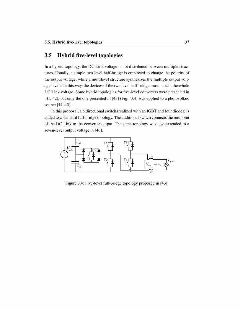
3.5 Hybrid five-level topologies . . . . . . . . . . . . . . . . . . . . . . 37
4 Novel Nine Level transformerless Inverter 39
4.1 Introduction . . . . . . . . . . . . . . . . . . . . . . . . . . . . . . 39

ii Summary
4.2 Architecture of the converter . . . . . . . . . . . . . . . . . . . . . 39
4.3 Flying Capacitor Voltage Regulation . . . . . . . . . . . . . . . . . 41
4.4 Application to transformerless photovoltaic converters . . . . . . . 46
4.5 DC Voltage independent modulation . . . . . . . . . . . . . . . . . 49
4.6 Simulation Results . . . . . . . . . . . . . . . . . . . . . . . . . . 49
4.7 Nine Level converter prototype . . . . . . . . . . . . . . . . . . . . 58
4.7.1 Control board . . . . . . . . . . . . . . . . . . . . . . . . . 58
4.7.2 Power board . . . . . . . . . . . . . . . . . . . . . . . . . 58
4.7.3 Output Stage Board . . . . . . . . . . . . . . . . . . . . . . 61
4.8 Experimental results . . . . . . . . . . . . . . . . . . . . . . . . . 66
5 Conclusions 77
Bibliography 79
List of Figures
1.1 Line-frequency transformer (a) and transformerless (b) inverter. . . . 3
1.2 High-frequency transformer inverter architecture [3]. . . . . . . . . 3
1.3 Block scheme of the control of a single-stage PV inverter. . . . . . . 4
1.4 Block scheme of the PLL in stationary reference frame. . . . . . . . 5
1.5 Block scheme of the transport delay PLL. . . . . . . . . . . . . . . 6
1.6 Block scheme of the SOGI-FLL. . . . . . . . . . . . . . . . . . . . 7
1.7 Frequency response of the SOGI filters. . . . . . . . . . . . . . . . 8
1.8 Model of the grid-connected converter with a LC filter. . . . . . . . 9
1.9 Bode response of the Plant with different values of the parameters. . 10
1.10 Bode response of the PR controller with different damping factors. . 11
1.11 Block scheme of the d-q current control for a single phase VSI. . . . 13
1.12 Scheme of the controller with the system affected by multiplicative
uncertainty. . . . . . . . . . . . . . . . . . . . . . . . . . . . . . . 15
1.13 Autonomous system employed to study the asymptotic stability. . . 15
1.14 Equivalent circuit of a PV cell. . . . . . . . . . . . . . . . . . . . . 17
1.15 Voltage-Current characteristic of a PV field. . . . . . . . . . . . . . 18
1.16 Voltage-Power characteristic of a PV field. . . . . . . . . . . . . . . 19
2.1 Full-bridge inverter with PV DC source. . . . . . . . . . . . . . . . 22
2.2 Model of the full-bridge converter. . . . . . . . . . . . . . . . . . . 23
2.3 Passive filter for ground leakage current reduction in a full-bridge
inverter. . . . . . . . . . . . . . . . . . . . . . . . . . . . . . . . . 24
iv List of Figures
2.4 Full-bridge with AC decoupling (HERIC) and DC decoupling (H5)
blocks. . . . . . . . . . . . . . . . . . . . . . . . . . . . . . . . . . 25
2.5 H6-type topology proposed in [16] . . . . . . . . . . . . . . . . . . 26
2.6 Topology proposed in [17]. . . . . . . . . . . . . . . . . . . . . . . 27
2.7 Topology proposed in [18] . . . . . . . . . . . . . . . . . . . . . . 28
2.8 Topology proposed in [19] . . . . . . . . . . . . . . . . . . . . . . 29
2.9 The H6 topology . . . . . . . . . . . . . . . . . . . . . . . . . . . 30
2.10 Topology proposed in [22]. . . . . . . . . . . . . . . . . . . . . . . 31
2.11 Topology proposed in [23]. . . . . . . . . . . . . . . . . . . . . . . 32
3.1 Five-level NPC Inverters: diode clamped (a) and flying capacitor (b). 34
3.2 Cascaded full-bridge with independent power supplies. . . . . . . . 35
3.3 NPC full-bridge five-level inverter. . . . . . . . . . . . . . . . . . . 36
3.4 Five-level full-bridge topology proposed in [43]. . . . . . . . . . . . 37
4.1 Cascaded full-bridge with flying capacitor. . . . . . . . . . . . . . . 41
4.2 Operating zones of the proposed PWM modulation when Vf c < 0.5VDC. 42
4.3 Operating zones of the proposed PWM modulation when Vf c > 0.5VDC. 42
4.4 Flying capacitor charge. . . . . . . . . . . . . . . . . . . . . . . . . 43
4.5 Flying capacitor discharge. . . . . . . . . . . . . . . . . . . . . . . 44
4.6 Flying capacitor control behavior with unity power factor. . . . . . . 45
4.7 Flying capacitor control behavior with different values of power factor. 46
4.8 Proposed topology. . . . . . . . . . . . . . . . . . . . . . . . . . . 47
4.9 Transient Circuit (TC) . . . . . . . . . . . . . . . . . . . . . . . . 48
4.10 Transient Circuit example waveforms. . . . . . . . . . . . . . . . . 49
4.11 Grid voltage and current with Vf c = 180V . . . . . . . . . . . . . . . 50
4.12 Converter output voltage, HVFB and LVFB output voltages and Fly-
ing capacitor voltage with Vf c = 180V . . . . . . . . . . . . . . . . . 51
4.13 Grid voltage and current with Vf c = 150V . . . . . . . . . . . . . . . 52
4.14 Converter output voltage, HVFB and LVFB output voltages and Fly-
ing capacitor voltage with Vf c = 150V . . . . . . . . . . . . . . . . . 53
4.15 Grid voltage and current with Vf c = 100V . . . . . . . . . . . . . . . 54
List of Figures v
4.16 Converter output voltage, HVFB and LVFB output voltages and Fly-
ing capacitor voltage with Vf c = 100V . . . . . . . . . . . . . . . . . 55
4.17 Ground voltage and current with ideal grid, iground = 25mARMS. . . . 56
4.18 Ground voltage and current with non ideal grid, iground = 47mARMS. 56
4.19 Ground voltage and current with non ideal grid and simple common
mode filter, iground = 30mARMS. . . . . . . . . . . . . . . . . . . . . 57
4.20 Gate driver circuit with insulated power supply. . . . . . . . . . . . 59
4.21 Circuit employed to measure the DC Link voltages with the optolin-
ear coupler. . . . . . . . . . . . . . . . . . . . . . . . . . . . . . . 60
4.22 Example circuit of the flyback converter from the TOP257-PN datasheet. 61
4.23 Schematic of the output filter. . . . . . . . . . . . . . . . . . . . . . 62
4.24 Intrinsic safety circuit. . . . . . . . . . . . . . . . . . . . . . . . . 63
4.25 Circuit for the phase-neutral detection. . . . . . . . . . . . . . . . . 64
4.26 Picture of the prototype with the boards separated. . . . . . . . . . . 65
4.27 Picture of the prototype with the stacked boards. . . . . . . . . . . . 65
4.28 Experimental test bed. . . . . . . . . . . . . . . . . . . . . . . . . 66
4.29 Converter output voltage and current with Vf c = 0.5VDC and unity
power factor. . . . . . . . . . . . . . . . . . . . . . . . . . . . . . 67
4.30 HVFB and LVFB output voltages with Vf c = 0.5VDC and unity power
factor. . . . . . . . . . . . . . . . . . . . . . . . . . . . . . . . . . 68
4.31 Converter output voltage and current with Vf c = 0.5VDC and PF=0.85. 69
4.32 HVFB and LVFB output voltages with Vf c = 0.5VDC and PF=0.85. . 70
4.33 Converter output voltage and current with Vf c = 0.33VDC and unity
power factor. . . . . . . . . . . . . . . . . . . . . . . . . . . . . . 71
4.34 HVFB and LVFB output voltages with Vf c = 0.33VDC and unity power
factor. . . . . . . . . . . . . . . . . . . . . . . . . . . . . . . . . . 71
4.35 Converter output voltage and current with Vf c = 0.66VDC and unity
power factor. . . . . . . . . . . . . . . . . . . . . . . . . . . . . . 72
4.36 HVFB and LVFB output voltages with Vf c = 0.66VDC and unity power
factor. . . . . . . . . . . . . . . . . . . . . . . . . . . . . . . . . . 72
4.37 Converter output voltage and current with Vf c = 0.66VDC and PF=0.85. 73

vi List of Figures
4.38 HVFB and LVFB output voltages with Vf c = 0.66VDC and PF=0.85. 73
4.39 Grid current and voltage in case of unipolar PWM and PF=0.1. . . . 74
4.40 Common mode voltage at the output of the converter in case of unipo-
lar PWM. . . . . . . . . . . . . . . . . . . . . . . . . . . . . . . . 74
4.41 Common mode voltage at the output of the converter in case of unipo-
lar PWM. . . . . . . . . . . . . . . . . . . . . . . . . . . . . . . . 75

Chapter 1
Overview of Photovoltaic systems
1.1 Introduction
The increasing demand for electrical power, along with the decreasing stock of tra-
ditional energy sources, has caused a growing interest towards microgeneration from
renewable power sources.
In particular, photovoltaic energy (PV) has witnessed an increasing attention and
the scientific community has concentrated its efforts in order to develop innovative
solutions for the integration of PV systems into the existing distribution grid.
PV systems can be mainly classified into two categories: stand-alone or grid-
connected. The first topology is suited for remote locations where the PV panels
power a local load, while grid-connected systems work in conjunction with the exist-
ing electrical grid.
Obviously, considering the highly discontinuous output of a PV field during a
day, in a stand-alone system suitable electric energy storage must be provided. More-
over, when the accumulators are fully charged, no more power can be extracted from
the panels. A grid-connected system does not suffer from these drawbacks, as the
maximum power available from the field can be continuously transferred to the grid.
Considering that the majority of the systems is of the grid-connected kind, a lot of re-
search was done in this field. For this reason, this thesis is focused on grid-connected

2 Chapter 1. Overview of Photovoltaic systems
converters for PV systems.
1.2 Grid-connected PV systems
The earlier designs of PV grid-connected inverters featured a full-bridge topology
coupled to the mains with a line frequency transformer (Fig. 1.1a). The transformer
guarantees the galvanic isolation between the PV field and the grid, simplifies the out-
put filter design and the compliance with the electromagnetic interference (EMI) in-
ternational regulations. However, converters embedding a line frequency transformer
are bulky and the transformer accounts for 1-2% of the power losses.
For these reasons, researchers have been active in studying solutions for the re-
moval of the line frequency transformer, in order to pursue the maximum efficiency
without increasing the converter cost.
The main issue that arises when the line frequency transformer is removed is due
to the presence of a parasitic capacitance between the metal frame of the panel and
the photovoltaic cells. The value of the capacitance varies with the ambient condi-
tions and with the panel technology. The typical value can range from 100 nF/kWp
for crystalline silicon to 1 µF/kWp for thin-film panels. This implies that a com-
mon mode current (i.e., ground leakage current) can flow into the resonant circuit
composed of the line conductors, the earth connection of the MV/LV distribution
transformer and the parasitic capacitance of the PV field [1].
If a simple full-bridge is employed without any transformer coupling or specific
modulation strategy, the high-frequency common mode voltage variations at the con-
verter output cause unacceptable levels of ground leakage current, that generate EMI,
reduce the safety of the system and cause the disconnection of the converter due to
the Residual Current Device (RCD) [2].
In order to solve the problem, two approaches were pursued: the transformer-
less (Fig. 1.1b) converter and the high-frequency transformer (Fig. 1.2) converter. In
the latter kind of topology, a high-frequency transformer is employed to transfer the
power from the PV panels to a DC/AC converter. Different choices for the converter
are possible: in [3] a soft-switching DC/DC converter feeds a full-bridge VSI and in

1.2. Grid-connected PV systems 3
[4] a resonant DC/DC converter is followed by a current source inverter.
DCV grid
vDC
V gridv
LFTransformer
( )b( )a
Figure 1.1: Line-frequency transformer (a) and transformerless (b) inverter.
gridv
DCV
HFTransformer
Figure 1.2: High-frequency transformer inverter architecture [3].
While the high-frequency transformer converter still guarantees the galvanic iso-
lation and is suitable for every kind of PV source, even for those panels that require
the grounding of the positive or the negative terminal, the transformerless approach
does not feature any transformer nor the galvanic isolation.
Transformerless inverters are usually designed for a precise panel technology.
For crystal and polycrystalline silicon, the main issue is the common mode voltage
variations at the converter output. In any case, for thin-film photovoltaic panels, it
is almost mandatory to employ insulated topologies, due to specific requirement of
the panel technology. In the following chapters several solutions are presented and
analyzed.
4 Chapter 1. Overview of Photovoltaic systems
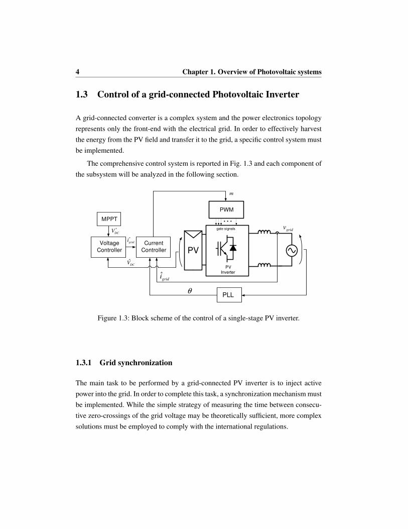
1.3 Control of a grid-connected Photovoltaic Inverter
A grid-connected converter is a complex system and the power electronics topology
represents only the front-end with the electrical grid. In order to effectively harvest
the energy from the PV field and transfer it to the grid, a specific control system must
be implemented.
The comprehensive control system is reported in Fig. 1.3 and each component of
the subsystem will be analyzed in the following section.
PWM
Voltage
Controller
MPPT
*
DCV
Current
Controller
*
gridi
ˆgridi
ˆDC
V
m
PVInverter
gate signals
PV
PLLθ
gridv
Figure 1.3: Block scheme of the control of a single-stage PV inverter.
1.3.1 Grid synchronization
The main task to be performed by a grid-connected PV inverter is to inject active
power into the grid. In order to complete this task, a synchronization mechanism must
be implemented. While the simple strategy of measuring the time between consecu-
tive zero-crossings of the grid voltage may be theoretically sufficient, more complex
solutions must be employed to comply with the international regulations.
1.3. Control of a grid-connected Photovoltaic Inverter 5
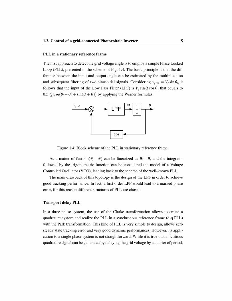
PLL in a stationary reference frame
The first approach to detect the grid voltage angle is to employ a simple Phase Locked
Loop (PLL), presented in the scheme of Fig. 1.4. The basic principle is that the dif-
ference between the input and output angle can be estimated by the multiplication
and subsequent filtering of two sinusoidal signals. Considering vgrid = Vg sinθi, it
follows that the input of the Low Pass Filter (LPF) is Vg sinθi cosθ , that equals to
0.5Vg (sin(θi −θ)+ sin(θi +θ)) by applying the Werner formulas.
LPF1
s
cos
θgridv ω
Figure 1.4: Block scheme of the PLL in stationary reference frame.
As a matter of fact sin(θi − θ) can be linearized as θi − θ , and the integrator
followed by the trigonometric function can be considered the model of a Voltage
Controlled Oscillator (VCO), leading back to the scheme of the well-known PLL.
The main drawback of this topology is the design of the LPF in order to achieve
good tracking performance. In fact, a first order LPF would lead to a marked phase
error, for this reason different structures of PLL are chosen.
Transport delay PLL
In a three-phase system, the use of the Clarke transformation allows to create a
quadrature system and realize the PLL in a synchronous reference frame (d-q PLL)
with the Park transformation. This kind of PLL is very simple to design, allows zero
steady state tracking error and very good dynamic performances. However, its appli-
cation to a single phase system is not straightforward. While it is true that a fictitious
quadrature signal can be generated by delaying the grid voltage by a quarter of period,
6 Chapter 1. Overview of Photovoltaic systems
this remains true only for a specific frequency, i.e., in case of frequency deviations a
tracking error appears.
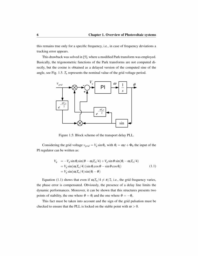
This drawback was solved in [5], where a modified Park transform was employed.
Basically, the trigonometric functions of the Park transforms are not computed di-
rectly, but the cosine is obtained as a delayed version of the computed sine of the
angle, see Fig. 1.5. Tn represents the nominal value of the grid voltage period.
gridv
sin
PI
2
nT s
e
π−
θωqV1
s
2
nT s
e
π−
Figure 1.5: Block scheme of the transport delay PLL.
Considering the grid voltage vgrid =Vg sinθi, with θi = ωit +Φ0 the input of the
PI regulator can be written as:
Vq =−Vg sinθi sin(θ −ωiTn/4)+Vg sinθ sin(θi −ωiTn/4)
=Vg sin(ωiTn/4)(sinθi cosθ − sinθ cosθi)
=Vg sin(ωiTn/4)sin(θi −θ)
(1.1)
Equation (1.1) shows that even if ωiTn/4 6= π/2, i.e., the grid frequency varies,
the phase error is compensated. Obviously, the presence of a delay line limits the
dynamic performances. Moreover, it can be shown that this structures presents two
points of stability, the one where θ = θi and the one where θ =−θi.
This fact must be taken into account and the sign of the grid pulsation must be
checked to ensure that the PLL is locked on the stable point with ω > 0.

1.3. Control of a grid-connected Photovoltaic Inverter 7
SOGI-FLL
A possible solution to employ a standard d-q PLL in a single phase grid was presented
in [6]. The basic idea is to realize a system able to generate the quadrature version of
a given input signal while tracking the frequency.
The core of the system is the Second Order Generalized Integrator (SOGI), that is
a second order transfer function with a resonance peak tuned to a specific frequency.
The block scheme is presented in Fig. 1.6.
1
s
1
s
fvqv
ffω
'ω
kgridv
1
s
−Γ
FLL
vε
Figure 1.6: Block scheme of the SOGI-FLL.
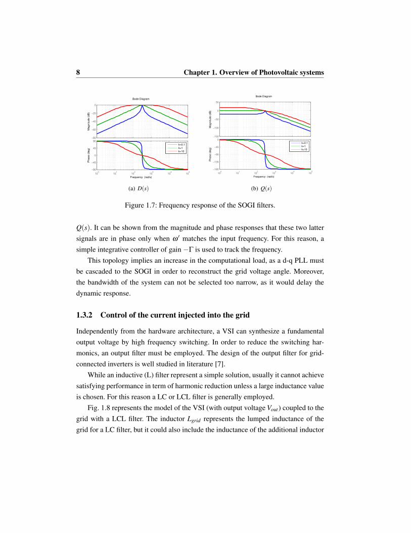
Neglecting the Frequency-Locked-Loop (FLL) and considering a fixed ω ′, the
transfer function between the outputs v f , vq and the input vgrid can be expressed as:
D(s) =v f (s)
vgrid(s)= kω ′s
s2+2kω ′s+ω ′2
Q(s) =vq(s)
vgrid(s)= kω ′2
s2+2kω ′s+ω ′2(1.2)
As it can be seen from the transfer functions (Fig. 1.7), v f represents a filtered
version of the input signal, while vq lags the input signal by π/2. The value ω ′ repre-
sents the resonance frequency, while the bandwidth of the filter is determined by the
value k.
The Frequency Locked Loop (FLL) dynamically tunes the resonance frequency
ω ′ of the SOGI. The mechanism resides in the transfer functions εv(s)/vgrid(s) and
8 Chapter 1. Overview of Photovoltaic systems
−80
−60
−40
−20
0
Magnitude (
dB
)
100
101
102
103
104
105
−90
−45
0
45
90
Phase (
deg)
Bode Diagram
Frequency (rad/s)
k=0.1
k=1
k=10
(a) D(s)
−150
−100
−50
0
50
Magnitude (
dB
)
100
101
102
103
104
105
−180
−135
−90
−45
0
Phase (
deg)
Bode Diagram
Frequency (rad/s)
k=0.1
k=1
k=10
(b) Q(s)
Figure 1.7: Frequency response of the SOGI filters.
Q(s). It can be shown from the magnitude and phase responses that these two latter
signals are in phase only when ω ′ matches the input frequency. For this reason, a
simple integrative controller of gain −Γ is used to track the frequency.
This topology implies an increase in the computational load, as a d-q PLL must
be cascaded to the SOGI in order to reconstruct the grid voltage angle. Moreover,
the bandwidth of the system can not be selected too narrow, as it would delay the
dynamic response.
1.3.2 Control of the current injected into the grid
Independently from the hardware architecture, a VSI can synthesize a fundamental
output voltage by high frequency switching. In order to reduce the switching har-
monics, an output filter must be employed. The design of the output filter for grid-
connected inverters is well studied in literature [7].
While an inductive (L) filter represent a simple solution, usually it cannot achieve
satisfying performance in term of harmonic reduction unless a large inductance value
is chosen. For this reason a LC or LCL filter is generally employed.
Fig. 1.8 represents the model of the VSI (with output voltage Vout) coupled to the
grid with a LCL filter. The inductor Lgrid represents the lumped inductance of the
grid for a LC filter, but it could also include the inductance of the additional inductor
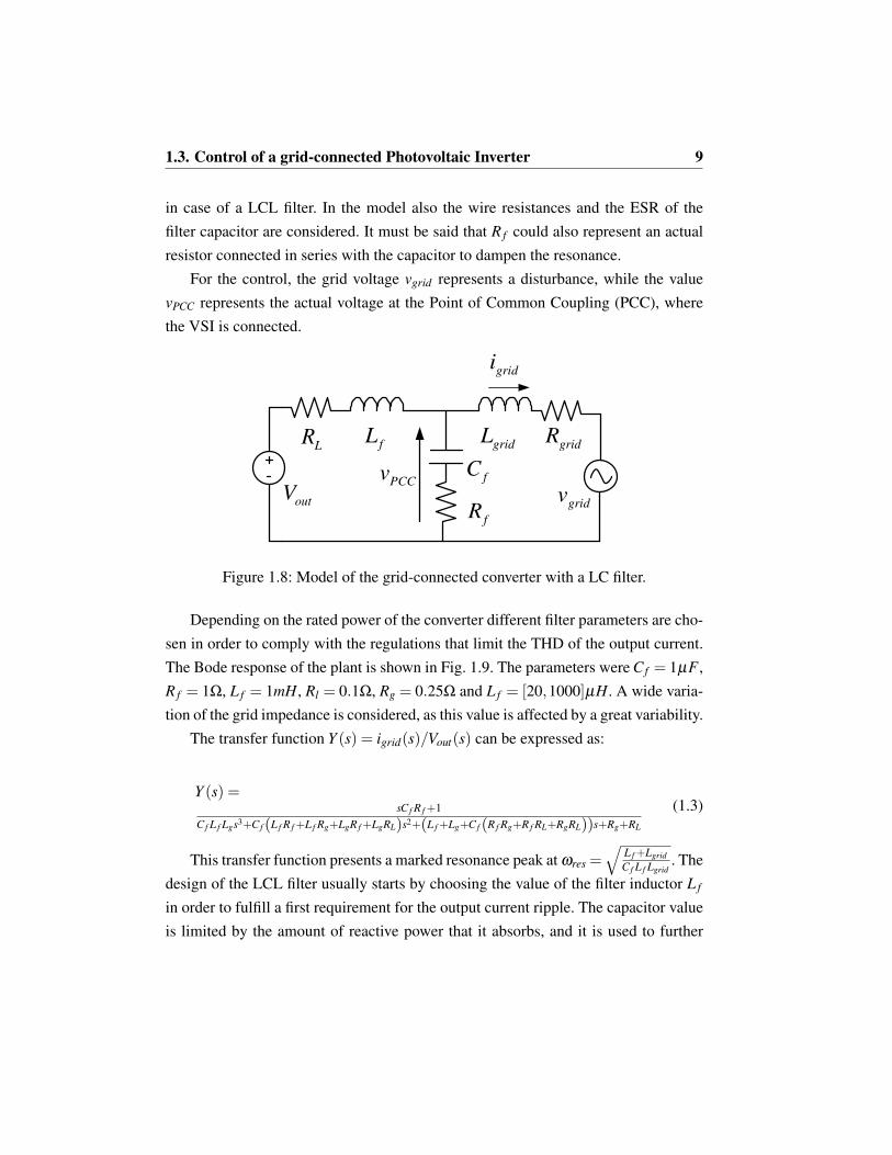
1.3. Control of a grid-connected Photovoltaic Inverter 9
in case of a LCL filter. In the model also the wire resistances and the ESR of the
filter capacitor are considered. It must be said that R f could also represent an actual
resistor connected in series with the capacitor to dampen the resonance.
For the control, the grid voltage vgrid represents a disturbance, while the value
vPCC represents the actual voltage at the Point of Common Coupling (PCC), where
the VSI is connected.
fL
LR
fR
fC
gridRgridL
gridv
PCCv
outV
gridi
Figure 1.8: Model of the grid-connected converter with a LC filter.
Depending on the rated power of the converter different filter parameters are cho-
sen in order to comply with the regulations that limit the THD of the output current.
The Bode response of the plant is shown in Fig. 1.9. The parameters were C f = 1µF ,
R f = 1Ω, L f = 1mH, Rl = 0.1Ω, Rg = 0.25Ω and L f = [20,1000]µH. A wide varia-
tion of the grid impedance is considered, as this value is affected by a great variability.
The transfer function Y (s) = igrid(s)/Vout(s) can be expressed as:
Y (s) =sC f R f +1
C f L f Lgs3+C f (L f R f +L f Rg+LgR f +LgRL)s2+(L f +Lg+C f (R f Rg+R f RL+RgRL))s+Rg+RL
(1.3)
This transfer function presents a marked resonance peak at ωres =√
L f +Lgrid
C f L f Lgrid. The
design of the LCL filter usually starts by choosing the value of the filter inductor L f
in order to fulfill a first requirement for the output current ripple. The capacitor value
is limited by the amount of reactive power that it absorbs, and it is used to further
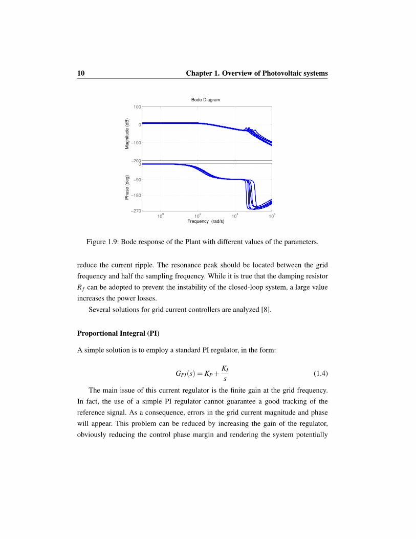
10 Chapter 1. Overview of Photovoltaic systems
−200
−100
0
100
Ma
gn
itu
de
(d
B)
100
102
104
106
−270
−180
−90
0
Ph
ase
(d
eg
)
Bode Diagram
Frequency (rad/s)
Figure 1.9: Bode response of the Plant with different values of the parameters.
reduce the current ripple. The resonance peak should be located between the grid
frequency and half the sampling frequency. While it is true that the damping resistor
R f can be adopted to prevent the instability of the closed-loop system, a large value
increases the power losses.
Several solutions for grid current controllers are analyzed [8].
Proportional Integral (PI)
A simple solution is to employ a standard PI regulator, in the form:
GPI(s) = KP +KI
s(1.4)
The main issue of this current regulator is the finite gain at the grid frequency.
In fact, the use of a simple PI regulator cannot guarantee a good tracking of the
reference signal. As a consequence, errors in the grid current magnitude and phase
will appear. This problem can be reduced by increasing the gain of the regulator,
obviously reducing the control phase margin and rendering the system potentially

1.3. Control of a grid-connected Photovoltaic Inverter 11
unstable.
Proportional Resonant (PR)
The steady state error at the grid frequency of the simple PI regulator is a serious
issue, as also the power factor of the output current cannot be controlled with preci-
sion.
The Proportional Resonant (PR) controller can overcome this problem, by de-
signing a second order controller with infinite gain at the grid frequency, as in (1.5).
In an actual implementation, some degree of damping must be introduced in the sys-
tem. This damping factor, k, regulates the gain of the resonant filter, as shown in Fig.
1.10.
GPR(s) = KI
ω2grid
s2 +ω2grid
≃ KI
ω2grid
s2 +2kωgrids+ω2grid
(1.5)
−100
−80
−60
−40
−20
0
20
Ma
gn
itu
de
(d
B)
100
101
102
103
104
105
−180
−135
−90
−45
0
Ph
ase
(d
eg
)
Bode Diagram
Frequency (rad/s)
k=0.1
k=0.2
k=1
k=2
Figure 1.10: Bode response of the PR controller with different damping factors.
The steady state performance of this controller depends on the choice of the
damping factor, that cannot be chosen too low in order to avoid system instability.

12 Chapter 1. Overview of Photovoltaic systems
Despite this problem, this controller is widely adopted when harmonic compensa-
tion is needed, as multiple PR controllers tuned to the fundamental harmonics can be
added together.
In the field of resonant controllers, the repetitive control was also considered for
actual implementations in grid-connected VSI [9]. The repetitive controller can be
viewed as positive feedback system with a delay line, that leads to the expression:
Grep(s) =Krep
1− e−Tns(1.6)
This controller shows infinite gain at the frequency 1/(Tn), i.e., the nominal grid
frequency, and its harmonics. Obviously, a specific compensator must be designed in
order to ensure the system stability.
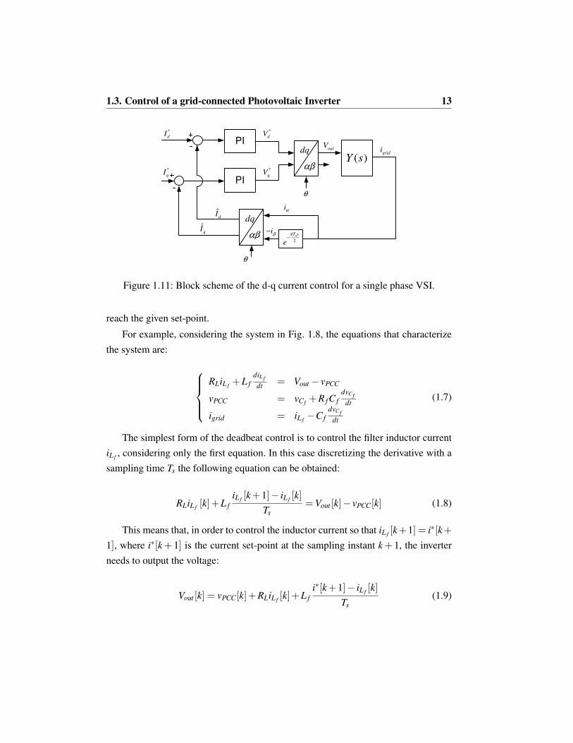
PI in synchronous reference frame
In a three phase system the synchronous current control in the d-q reference frame is
widely adopted. However, its application to a single phase system needs the genera-
tion of a fictitious quadrature system, as already explained in section 1.3.1.
Fig. 1.11 shows a possible implementation of the d-q grid current control. A delay
block is employed to generate the quadrature current signal, and a simple PI for each
axis is employed. Obviously, only one output of the Park inverse transform is chosen
as output voltage Vout . Depending on the convention chosen for the PLL, the active
power axis can be either the direct or the quadrature one.
This controller exhibits excellent steady state performance and possibility to con-
trol active or reactive power. However, the presence of a delay line negatively affects
its dynamic performance.
Deadbeat controller
The deadbeat controller is a model-based discrete control which aims at obtaining
zero steady state error in a finite number of sampling intervals.
The basic idea is to write the difference equation that governs the system’s dy-
namics, and to calculate the exact value of the controlled variable which allows to
1.3. Control of a grid-connected Photovoltaic Inverter 13
2
nT s
e
π−
PI
PI
αβ
dq outV
( )Y s
αβ
dq
θ
θ
ˆdI
ˆqI
*
dI
*
qI
gridi
iα
iβ−
*
dV
*
qV
Figure 1.11: Block scheme of the d-q current control for a single phase VSI.
reach the given set-point.
For example, considering the system in Fig. 1.8, the equations that characterize
the system are:
RLiL f+L f
diL f
dt= Vout − vPCC
vPCC = vC f+R fC f
dvCf
dt
igrid = iL f−C f
dvCf
dt
(1.7)
The simplest form of the deadbeat control is to control the filter inductor current
iL f, considering only the first equation. In this case discretizing the derivative with a
sampling time Ts the following equation can be obtained:
RLiL f[k]+L f
iL f[k+1]− iL f
[k]
Ts
=Vout [k]− vPCC[k] (1.8)
This means that, in order to control the inductor current so that iL f[k+1] = i∗[k+
1], where i∗[k+ 1] is the current set-point at the sampling instant k+ 1, the inverter
needs to output the voltage:
Vout [k] = vPCC[k]+RLiL f[k]+L f
i∗[k+1]− iL f[k]
Ts
(1.9)
14 Chapter 1. Overview of Photovoltaic systems
From (1.9) the control needs to know the desired current one sample time ahead:
i∗[k+1].
However, the control is complicated by the fact that a PWM inverter operates
intrinsically with a time delay of one step, so it is not possible to control the inductor
current at the next sample time. An additional sampling interval is needed to take
into account this delay and all the variables at the next sampling interval must be
predicted.
In fact, Vout [k] at the instant k was decided at the previous step, so the control must
calculate the value Vout [k+ 1], that can be obtained shifting into the future equation
(1.9). The same equation can be employed to predict iL f[k+1].
The final form of the deadbeat controller, including the delay in the PWM inverter
is given by (1.10)
iL f[k+1] = Ts
L f
(
Vout [k]− vPCC[k]−RLiL f[k]
)
+ iL f[k]
Vout [k+1] = vPCC[k+1]+RLiL f[k+1]+L f
i∗[k+2]−iL f[k+1]
Ts
(1.10)
To implement the control in (1.10) it is necessary to predict the values vPCC[k+1]
and i∗[k+2]. Different approaches are feasible, i.e. circular buffers to predict periodic
signals or data interpolations. The way the predictions are calculated affects in a
marked way the performance of the control [10].
Moreover, the deadbeat control needs a good knowledge of the system model,
and errors in the system parameters affect the set-point tracking and can also lead to
the instability of the control.
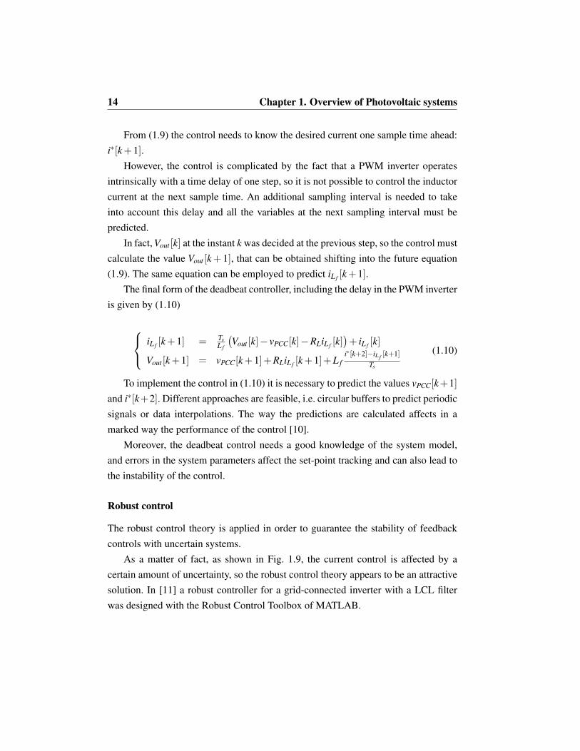
Robust control
The robust control theory is applied in order to guarantee the stability of feedback
controls with uncertain systems.
As a matter of fact, as shown in Fig. 1.9, the current control is affected by a
certain amount of uncertainty, so the robust control theory appears to be an attractive
solution. In [11] a robust controller for a grid-connected inverter with a LCL filter
was designed with the Robust Control Toolbox of MATLAB.
1.3. Control of a grid-connected Photovoltaic Inverter 15
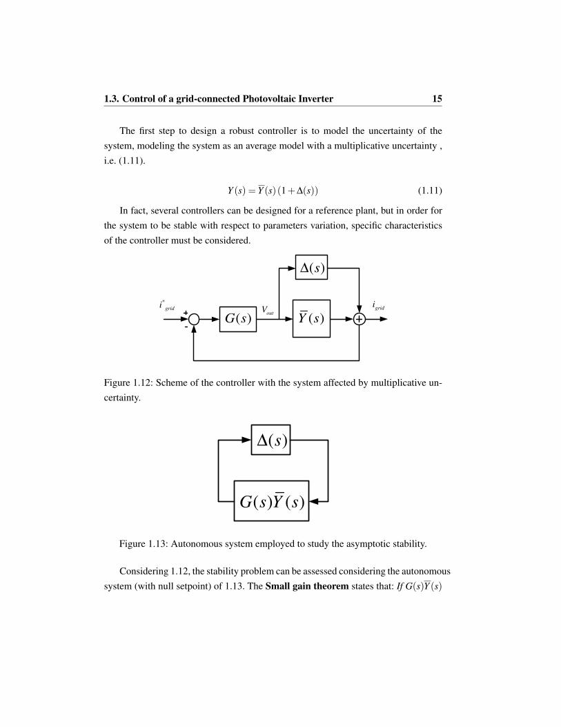
The first step to design a robust controller is to model the uncertainty of the
system, modeling the system as an average model with a multiplicative uncertainty ,
i.e. (1.11).
Y (s) = Y (s)(1+∆(s)) (1.11)
In fact, several controllers can be designed for a reference plant, but in order for
the system to be stable with respect to parameters variation, specific characteristics
of the controller must be considered.
( )Y sgrid
i
( )s∆
( )G soutV
*
gridi
Figure 1.12: Scheme of the controller with the system affected by multiplicative un-
certainty.
( )s∆
( ) ( )G s Y s
Figure 1.13: Autonomous system employed to study the asymptotic stability.
Considering 1.12, the stability problem can be assessed considering the autonomous
system (with null setpoint) of 1.13. The Small gain theorem states that: If G(s)Y (s)

16 Chapter 1. Overview of Photovoltaic systems
and ∆(s) are stable, system of 1.13 is asymptotically stable if:
‖ GY ∆ ‖< 1 (1.12)
That is equivalent to say:
σ(
G( jω)Y ( jω)∆( jω))
< 1 (1.13)
where σ represents the singular value for a multivariable transfer function. In
the case of Single-Input Single-Output system the singular value is equivalent to the
maximum absolute value of the transfer function over the frequency range.
It follows that the robust stability is guaranteed if
σ(
G( jω)Y ( jω))
<1
∆( jω)(1.14)
In other words, the maximum amount of uncertainty of the system limits the
maximum gain (therefore the performance) of the feedback system. Usually it is im-
portant to shape the robust controller in order to guarantee specific characteristic, i.e.
high gain in the frequency range of interest. In fact, the transfer function can incor-
porate specific weighing filters.
For this reason a mixed sensitivity problem is generally formulated and con-
trollers with fairly good characteristics can be designed [11].
The main drawback of this kind of design is that too wide variations of the pa-
rameters compromise excessively the performance of the designed controller.
1.3.3 Maximum Power Point Tracking
The current control represents the basic functionality of the grid-connected inverter.
In fact, depending on the system architecture, one or more control loops are needed
in order to achieve the full functionality.
In particular, for a single-stage DC/AC inverter, the DC Link is directly connected
to the photovoltaic field, and it is mandatory to control the DC Link voltage.
The control of the DC Link voltage can be realized controlling the current injected
into the grid. The DC Link voltage then follows the well-known characteristic of the
1.3. Control of a grid-connected Photovoltaic Inverter 17
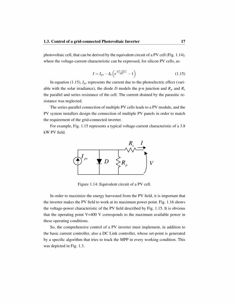
photovoltaic cell, that can be derived by the equivalent circuit of a PV cell (Fig. 1.14),
where the voltage-current characteristic can be expressed, for silicon PV cells, as:
I = Ipv − I0
(
eq(V+RsI)
nkT −1)
(1.15)
In equation (1.15), Ipv represents the current due to the photoelectric effect (vari-
able with the solar irradiance), the diode D models the p-n junction and Rp and Rs
the parallel and series resistance of the cell. The current drained by the parasitic re-
sistance was neglected.
The series-parallel connection of multiple PV cells leads to a PV module, and the
PV system installers design the connection of multiple PV panels in order to match
the requirement of the grid-connected inverter.
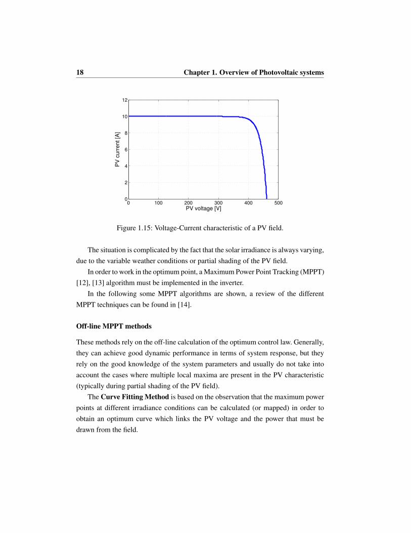
For example, Fig. 1.15 represents a typical voltage-current characteristic of a 3.8
kW PV field.
pvI
pR
sR
V
I
D
Figure 1.14: Equivalent circuit of a PV cell.
In order to maximize the energy harvested from the PV field, it is important that
the inverter makes the PV field to work at its maximum power point. Fig. 1.16 shows
the voltage-power characteristic of the PV field described by Fig. 1.15. It is obvious
that the operating point V=400 V corresponds to the maximum available power in
these operating conditions.
So, the comprehensive control of a PV inverter must implement, in addition to
the basic current controller, also a DC Link controller, whose set-point is generated
by a specific algorithm that tries to track the MPP in every working condition. This
was depicted in Fig. 1.3.
18 Chapter 1. Overview of Photovoltaic systems
0 100 200 300 400 5000
2
4
6
8
10
12
PV voltage [V]
PV
curr
ent [A
]
Figure 1.15: Voltage-Current characteristic of a PV field.
The situation is complicated by the fact that the solar irradiance is always varying,
due to the variable weather conditions or partial shading of the PV field.
In order to work in the optimum point, a Maximum Power Point Tracking (MPPT)
[12], [13] algorithm must be implemented in the inverter.
In the following some MPPT algorithms are shown, a review of the different
MPPT techniques can be found in [14].
Off-line MPPT methods
These methods rely on the off-line calculation of the optimum control law. Generally,
they can achieve good dynamic performance in terms of system response, but they
rely on the good knowledge of the system parameters and usually do not take into
account the cases where multiple local maxima are present in the PV characteristic
(typically during partial shading of the PV field).
The Curve Fitting Method is based on the observation that the maximum power
points at different irradiance conditions can be calculated (or mapped) in order to
obtain an optimum curve which links the PV voltage and the power that must be
drawn from the field.

1.3. Control of a grid-connected Photovoltaic Inverter 19
0 100 200 300 400 5000
500
1000
1500
2000
2500
3000
3500
4000
PV voltage [V]
PV
pow
er
[V]
Figure 1.16: Voltage-Power characteristic of a PV field.
The Fractional Short Circuit Current/Fractional Open Circuit Voltage method
relies on the fact that the MPP current or voltage follows in first approximation a
linear law. By measuring at different time instants the open circuit voltage or short
circuit current the MPP law can be updated.
On-line MPPT methods
These algorithms search for the optimum operating point continuously and they do
not rely only on precalculated characteristics.
The Perturb and Observe (P&O) algorithm is one of the most employed due to
the ease of implementation and the fact that it requires very little tuning. It is based on
the continuous perturbation of the system operating point in the attempt to move the
system towards the increasing power. In steady-state conditions, the algorithm oscil-
lates around the maximum power point, inverting the sign of the perturbation at every
sampling interval. This behavior also represents the main drawback of this method,
as in order to achieve good MPP tracking the perturbation must be sufficiently high,
but the higher the perturbation, the higher the oscillation around the MPP at steady
state, and consequently the lower the MPP tracking efficiency.

20 Chapter 1. Overview of Photovoltaic systems
In order to solve the drawback of the P&O method various approaches where
investigated, where basically the magnitude of the perturbation is adapted in order to
obtain good tracking performance with little steady-state oscillation.
Chapter 2
State of the art of transformerless
PV Inverters
2.1 Transformerless Full-Bridge topologies
In this section the full-bridge solutions that address the problem of high-frequency
common mode voltage variations are analyzed.
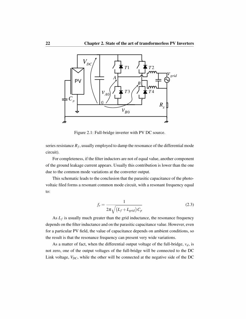
Fig. 2.1 shows a full-bridge converter powered by a PV source. Assuming the
negative side of the DC Link as the reference potential, vA0 and vB0 can be defined as
the outputs of the full-bridge. The common mode voltage can be expressed as (2.1),
while the differential voltage is the difference between the two potentials (2.2).
vcm =vA0 + vB0
2(2.1)
vd = vA0 − vB0 (2.2)
In order to explain the cause of the common mode current, the full-bridge can
be modeled as a differential and a common mode voltage sources, as in Fig. 2.2.
In the same figure also the grid impedance is shown (Rgrid and Lgrid), along with
the parasitic resistance RL of the filter inductor L f and the filter capacitor (C f with a
22 Chapter 2. State of the art of transformerless PV Inverters
1T 2T
3T 4T
PV
0
0Av
AB
0Bv
gridv
DCV
gR
pC
Figure 2.1: Full-bridge inverter with PV DC source.
series resistance R f , usually employed to damp the resonance of the differential mode
circuit).
For completeness, if the filter inductors are not of equal value, another component
of the ground leakage current appears. Usually this contribution is lower than the one
due to the common mode variations at the converter output.
This schematic leads to the conclusion that the parasitic capacitance of the photo-
voltaic filed forms a resonant common mode circuit, with a resonant frequency equal
to:
fr =1
2π√
(
L f +Lgrid
)
Cp
(2.3)
As L f is usually much greater than the grid inductance, the resonance frequency
depends on the filter inductance and on the parasitic capacitance value. However, even
for a particular PV field, the value of capacitance depends on ambient conditions, so
the result is that the resonance frequency can present very wide variations.
As a matter of fact, when the differential output voltage of the full-bridge, vd , is
not zero, one of the output voltages of the full-bridge will be connected to the DC
Link voltage, VDC, while the other will be connected at the negative side of the DC

2.1. Transformerless Full-Bridge topologies 23
gR
fL
fL
cmv
2dv
2dv
gridL
gridL
gridR
gridR
fR
fC
LR
LR
pC
gridv
Figure 2.2: Model of the full-bridge converter.
Link. The common mode voltage at the output will simply be equal to vcm =VDC/2.
During the current freewheeling, depending on the sign of the current, the differ-
ential voltage can be either zero (three level PWM) or ±VDC (bipolar modulation).
While with the bipolar modulation the common mode voltage is always vcm =VDC/2,
in the three level PWM it can be either VDC or 0V depending on the configuration of
the transistors.
With this premise, it is obvious that the bipolar modulation strategy (two level
output voltage) is ideally suitable for PV inverters. However, its poorer energy effi-
ciency, high output current ripple and common mode voltage variations (during the
mandatory dead-times between the commutations) make its application very limited.
For this reason, three level inverters are nowadays the most widely adopted solution,
although they require specific strategies for the common mode output voltage.
In the following different three level inverters are analyzed. All of them employ
different strategies to keep the common mode voltage to a constant level vcm =VDC/2.
They can be further divided into two kinds: the ones that fix the output of the full-
bridge to a known potential with active clamping, and the ones that rely on the tran-
sient behavior to achieve the same objective.
24 Chapter 2. State of the art of transformerless PV Inverters
It must be said that the reduction of the common mode output voltage is not
the only way that can be pursued to reduce the ground leakage currents. In fact, it
is sufficient to ensure that high-frequency voltage variations do not happen over the
photovoltaic field parasitic capacitance, such as with Neutral Point Clamped (NPC)
architectures. Some recent advances are reported in the last part of the chapter as
well.
For completeness, it must be said that the common mode current at the output of
a three level (unipolar PWM) inverter can be addressed also with a specific output
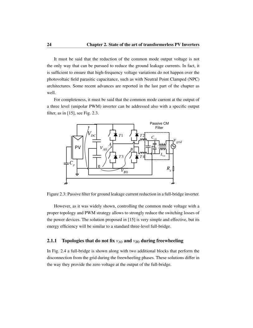
filter, as in [15], see Fig. 2.3.
1T 2T
3T 4T
PV
0
0Av
AB
0Bv
gridv
DCV
gRp
C0
cmL
cmC
Passive CM Filter
Figure 2.3: Passive filter for ground leakage current reduction in a full-bridge inverter.
However, as it was widely shown, controlling the common mode voltage with a
proper topology and PWM strategy allows to strongly reduce the switching losses of
the power devices. The solution proposed in [15] is very simple and effective, but its
energy efficiency will be similar to a standard three-level full-bridge.
2.1.1 Topologies that do not fix vA0 and vB0 during freewheeling
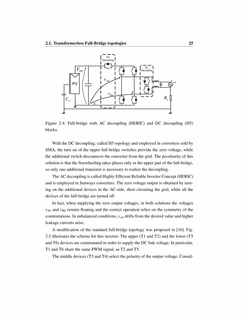
In Fig. 2.4 a full-bridge is shown along with two additional blocks that perform the
disconnection from the grid during the freewheeling phases. These solutions differ in
the way they provide the zero voltage at the output of the full-bridge.
2.1. Transformerless Full-Bridge topologies 25
A
B
gridvPV
AC
Decoupling
DC
Decoupling
0Av
0Bv
pC gR
DCV
0
Figure 2.4: Full-bridge with AC decoupling (HERIC) and DC decoupling (H5)
blocks.
With the DC decoupling, called H5 topology and employed in converters sold by
SMA, the turn on of the upper full-bridge switches provide the zero voltage, while
the additional switch disconnects the converter from the grid. The peculiarity of this
solution is that the freewheeling takes places only in the upper part of the full-bridge,
so only one additional transistor is necessary to realize the decoupling.
The AC decoupling is called Highly Efficient Reliable Inverter Concept (HERIC)
and is employed in Sunways converters. The zero voltage output is obtained by turn-
ing on the additional devices in the AC-side, short circuiting the grid, while all the
devices of the full-bridge are turned off.
In fact, when supplying the zero output voltages, in both solutions the voltages
vA0 and vB0 remain floating and the correct operation relies on the symmetry of the
commutations. In unbalanced conditions, vcm drifts from the desired value and higher
leakage currents arise.
A modification of the standard full-bridge topology was proposed in [16]. Fig.
2.5 illustrates the scheme for this inverter. The upper (T1 and T2) and the lower (T5
and T6) devices are commutated in order to supply the DC link voltage. In particular,
T1 and T6 share the same PWM signal, as T2 and T5.
The middle devices (T3 and T4) select the polarity of the output voltage. Consid-
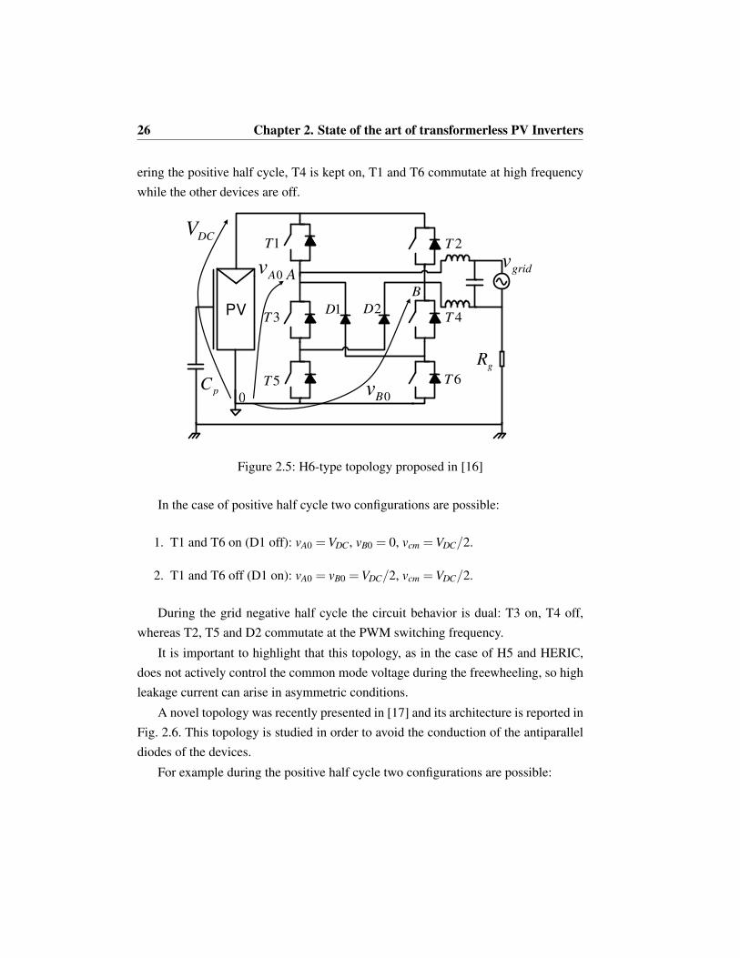
26 Chapter 2. State of the art of transformerless PV Inverters
ering the positive half cycle, T4 is kept on, T1 and T6 commutate at high frequency
while the other devices are off.
1T 2T
3T
5T
4T
6T
1D 2DPV
0
0Av A
B
0Bv
gridv
pC
DCV
gR
Figure 2.5: H6-type topology proposed in [16]
In the case of positive half cycle two configurations are possible:
1. T1 and T6 on (D1 off): vA0 =VDC, vB0 = 0, vcm =VDC/2.
2. T1 and T6 off (D1 on): vA0 = vB0 =VDC/2, vcm =VDC/2.
During the grid negative half cycle the circuit behavior is dual: T3 on, T4 off,
whereas T2, T5 and D2 commutate at the PWM switching frequency.
It is important to highlight that this topology, as in the case of H5 and HERIC,
does not actively control the common mode voltage during the freewheeling, so high
leakage current can arise in asymmetric conditions.
A novel topology was recently presented in [17] and its architecture is reported in
Fig. 2.6. This topology is studied in order to avoid the conduction of the antiparallel
diodes of the devices.
For example during the positive half cycle two configurations are possible:
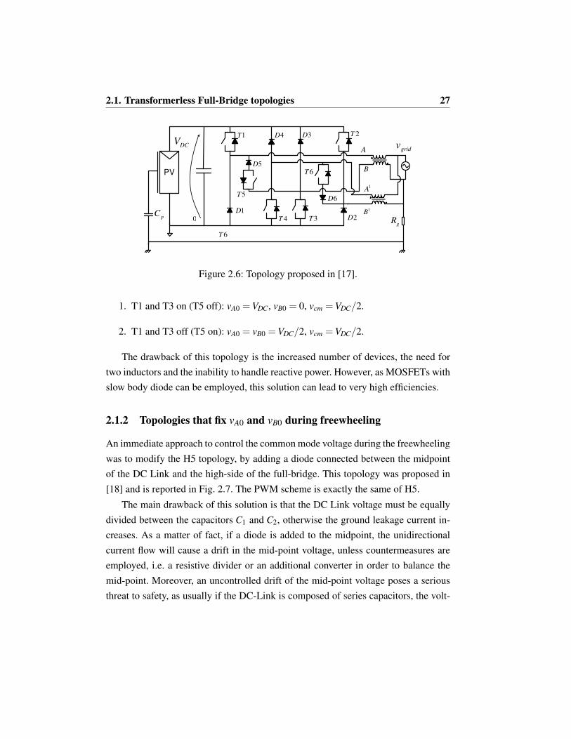
2.1. Transformerless Full-Bridge topologies 27
6T
PV
0pC
gridv
1T 2T
3T4T
5T
6T
1D2D
4D 3D
5D
6D
DCVA
B
1A
1B
gR
Figure 2.6: Topology proposed in [17].
1. T1 and T3 on (T5 off): vA0 =VDC, vB0 = 0, vcm =VDC/2.
2. T1 and T3 off (T5 on): vA0 = vB0 =VDC/2, vcm =VDC/2.
The drawback of this topology is the increased number of devices, the need for
two inductors and the inability to handle reactive power. However, as MOSFETs with
slow body diode can be employed, this solution can lead to very high efficiencies.
2.1.2 Topologies that fix vA0 and vB0 during freewheeling
An immediate approach to control the common mode voltage during the freewheeling
was to modify the H5 topology, by adding a diode connected between the midpoint
of the DC Link and the high-side of the full-bridge. This topology was proposed in
[18] and is reported in Fig. 2.7. The PWM scheme is exactly the same of H5.
The main drawback of this solution is that the DC Link voltage must be equally
divided between the capacitors C1 and C2, otherwise the ground leakage current in-
creases. As a matter of fact, if a diode is added to the midpoint, the unidirectional
current flow will cause a drift in the mid-point voltage, unless countermeasures are
employed, i.e. a resistive divider or an additional converter in order to balance the
mid-point. Moreover, an uncontrolled drift of the mid-point voltage poses a serious
threat to safety, as usually if the DC-Link is composed of series capacitors, the volt-
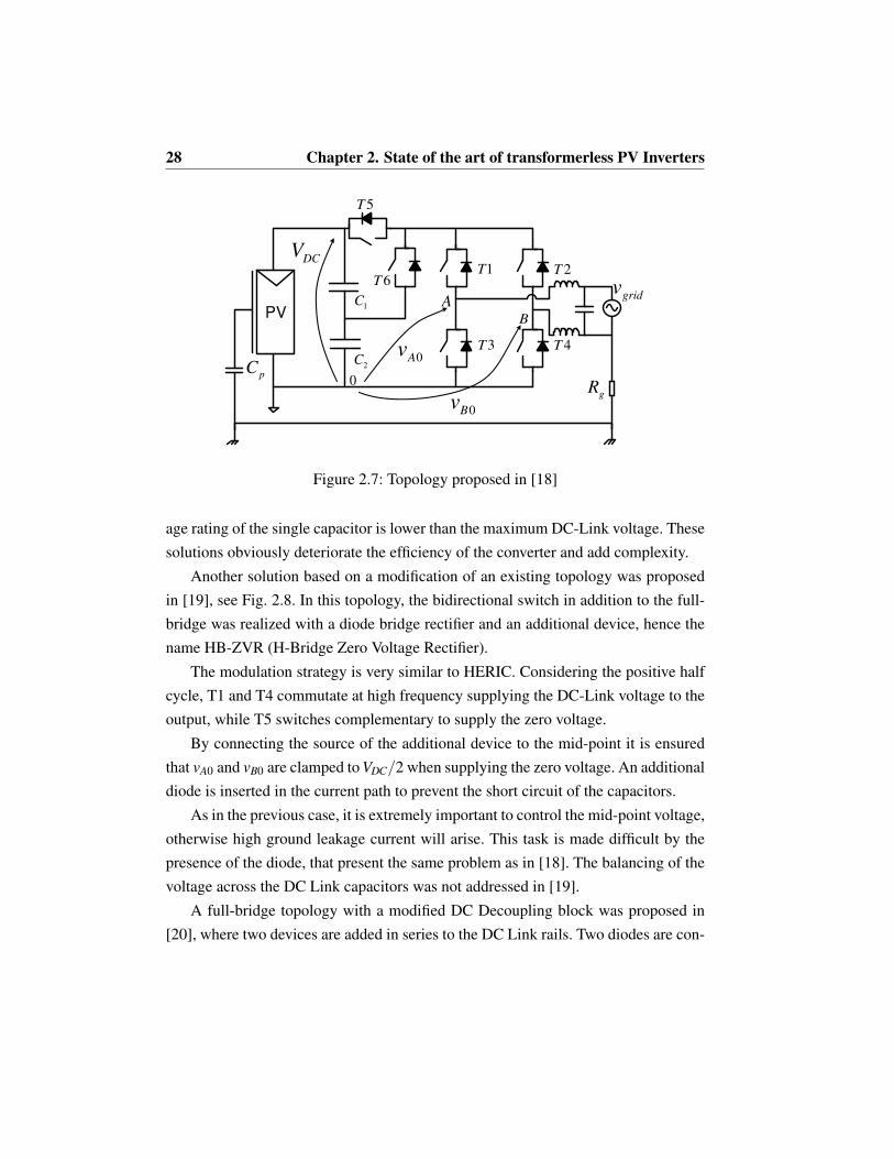
28 Chapter 2. State of the art of transformerless PV Inverters
1T 2T
3T
5T
4T
6T
PV
0
0Av
AB
0Bv
gridv
1C
2C
DCV
gR
pC
Figure 2.7: Topology proposed in [18]
age rating of the single capacitor is lower than the maximum DC-Link voltage. These
solutions obviously deteriorate the efficiency of the converter and add complexity.
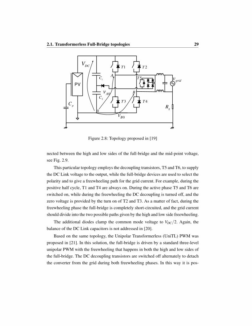
Another solution based on a modification of an existing topology was proposed
in [19], see Fig. 2.8. In this topology, the bidirectional switch in addition to the full-
bridge was realized with a diode bridge rectifier and an additional device, hence the
name HB-ZVR (H-Bridge Zero Voltage Rectifier).
The modulation strategy is very similar to HERIC. Considering the positive half
cycle, T1 and T4 commutate at high frequency supplying the DC-Link voltage to the
output, while T5 switches complementary to supply the zero voltage.
By connecting the source of the additional device to the mid-point it is ensured
that vA0 and vB0 are clamped to VDC/2 when supplying the zero voltage. An additional
diode is inserted in the current path to prevent the short circuit of the capacitors.
As in the previous case, it is extremely important to control the mid-point voltage,
otherwise high ground leakage current will arise. This task is made difficult by the
presence of the diode, that present the same problem as in [18]. The balancing of the
voltage across the DC Link capacitors was not addressed in [19].
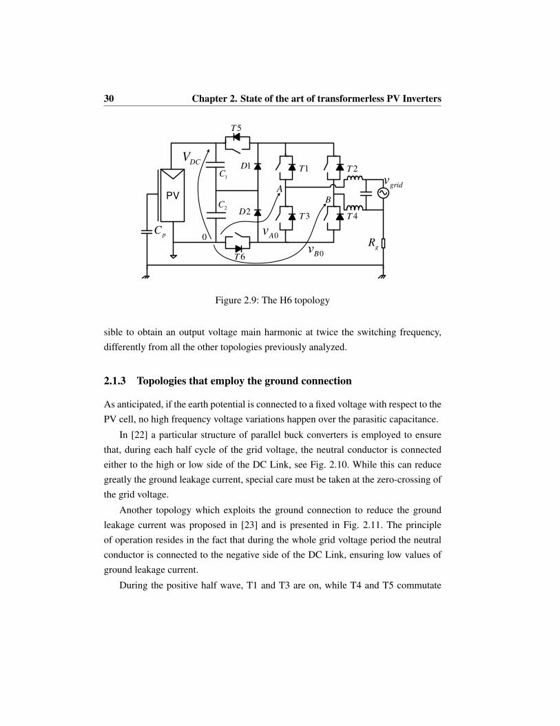
A full-bridge topology with a modified DC Decoupling block was proposed in
[20], where two devices are added in series to the DC Link rails. Two diodes are con-
2.1. Transformerless Full-Bridge topologies 29
1T 2T
3T 4T
PV
0
0Av
A
B
0Bv
gridv1C
2C
5T
DCV
gRp
C
Figure 2.8: Topology proposed in [19]
nected between the high and low sides of the full-bridge and the mid-point voltage,
see Fig. 2.9.
This particular topology employs the decoupling transistors, T5 and T6, to supply
the DC Link voltage to the output, while the full-bridge devices are used to select the
polarity and to give a freewheeling path for the grid current. For example, during the
positive half cycle, T1 and T4 are always on. During the active phase T5 and T6 are
switched on, while during the freewheeling the DC decoupling is turned off, and the
zero voltage is provided by the turn on of T2 and T3. As a matter of fact, during the
freewheeling phase the full-bridge is completely short-circuited, and the grid current
should divide into the two possible paths given by the high and low side freewheeling.
The additional diodes clamp the common mode voltage to VDC/2. Again, the
balance of the DC Link capacitors is not addressed in [20].
Based on the same topology, the Unipolar Transformerless (UniTL) PWM was
proposed in [21]. In this solution, the full-bridge is driven by a standard three-level
unipolar PWM with the freewheeling that happens in both the high and low sides of
the full-bridge. The DC decoupling transistors are switched off alternately to detach
the converter from the grid during both freewheeling phases. In this way it is pos-
30 Chapter 2. State of the art of transformerless PV Inverters
1T 2T
3T
5T
4T
6T
PV
0 0Av
AB
0Bv
gridv1C
2C
DCV
gR
pC
1D
2D
Figure 2.9: The H6 topology
sible to obtain an output voltage main harmonic at twice the switching frequency,
differently from all the other topologies previously analyzed.
2.1.3 Topologies that employ the ground connection
As anticipated, if the earth potential is connected to a fixed voltage with respect to the
PV cell, no high frequency voltage variations happen over the parasitic capacitance.
In [22] a particular structure of parallel buck converters is employed to ensure
that, during each half cycle of the grid voltage, the neutral conductor is connected
either to the high or low side of the DC Link, see Fig. 2.10. While this can reduce
greatly the ground leakage current, special care must be taken at the zero-crossing of
the grid voltage.
Another topology which exploits the ground connection to reduce the ground
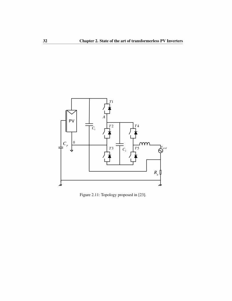
leakage current was proposed in [23] and is presented in Fig. 2.11. The principle
of operation resides in the fact that during the whole grid voltage period the neutral
conductor is connected to the negative side of the DC Link, ensuring low values of
ground leakage current.
During the positive half wave, T1 and T3 are on, while T4 and T5 commutate
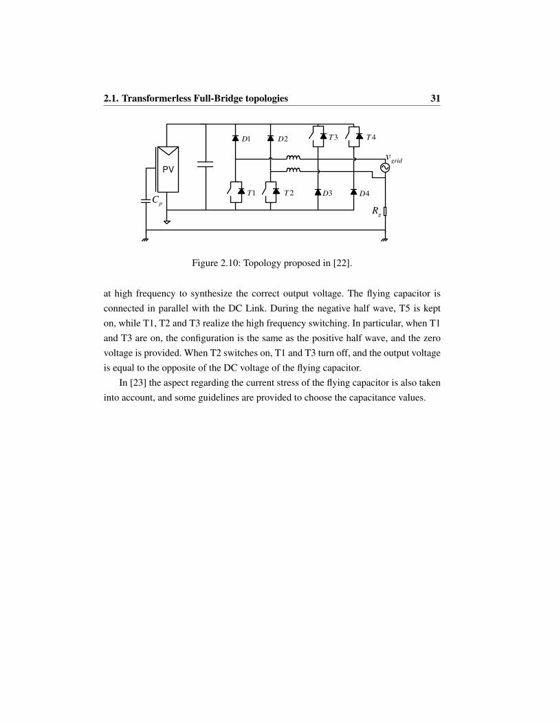
2.1. Transformerless Full-Bridge topologies 31
PV
pC
gridv
gR
1T
3T
2T
4T1D 2D
3D 4D
Figure 2.10: Topology proposed in [22].
at high frequency to synthesize the correct output voltage. The flying capacitor is
connected in parallel with the DC Link. During the negative half wave, T5 is kept
on, while T1, T2 and T3 realize the high frequency switching. In particular, when T1
and T3 are on, the configuration is the same as the positive half wave, and the zero
voltage is provided. When T2 switches on, T1 and T3 turn off, and the output voltage
is equal to the opposite of the DC voltage of the flying capacitor.
In [23] the aspect regarding the current stress of the flying capacitor is also taken
into account, and some guidelines are provided to choose the capacitance values.
32 Chapter 2. State of the art of transformerless PV Inverters
1T
2T
PV
0
A
1C
gR
pC
2C gridv
3T
4T
5T
Figure 2.11: Topology proposed in [23].

Chapter 3
State of the art of Multilevel
Inverter topologies
3.1 Introduction
Multilevel converters ensure a better reconstruction of the output waveform, allow
to reduce the size of output filters and increase the converter efficiency. Research on
multilevel converters has been going on for several years [24], but only recently they
have been applied to PV converters [25, 26, 27].
The basic idea is that the DC Link voltage can be split across different capacitors,
that can provide intermediate voltage levels between the reference potential and the
DC Link voltage [28]. Numerous solutions for multilevel inverters are present in
literature; in the following a review of the state of the art is reported, with reference
to a five-level output voltage. However, most of the topologies could be extended to
a greater number of output voltage levels.
As the focus of this work is on single phase (i.e. not high voltage) photovoltaic
systems, only some of the numerous ideas presented in literature are reported.
34 Chapter 3. State of the art of Multilevel Inverter topologies
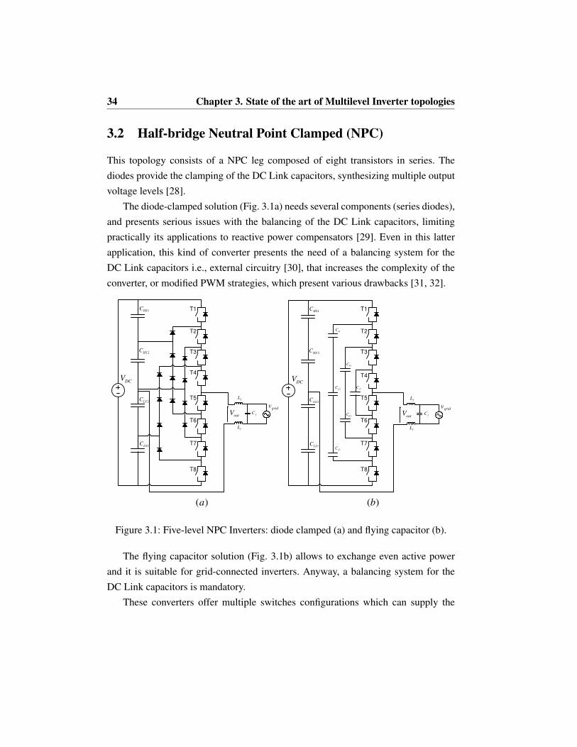
3.2 Half-bridge Neutral Point Clamped (NPC)
This topology consists of a NPC leg composed of eight transistors in series. The
diodes provide the clamping of the DC Link capacitors, synthesizing multiple output
voltage levels [28].
The diode-clamped solution (Fig. 3.1a) needs several components (series diodes),
and presents serious issues with the balancing of the DC Link capacitors, limiting
practically its applications to reactive power compensators [29]. Even in this latter
application, this kind of converter presents the need of a balancing system for the
DC Link capacitors i.e., external circuitry [30], that increases the complexity of the
converter, or modified PWM strategies, which present various drawbacks [31, 32].
DCV
1HSC
2HSC
2LSC
1LSC
DCV
1HSC
2HSC
2LSC
1LSC
1aC
2aC
3aC
1bC
2bC
1cC
( )a ( )b
T1
T2
T3
T4
T5
T6
T7
T8
T2
T3
T4
T5
T6
T7
T8
fL
fL
gridv
fC
outV
fL
fL
gridv
fCout
V
T1
Figure 3.1: Five-level NPC Inverters: diode clamped (a) and flying capacitor (b).
The flying capacitor solution (Fig. 3.1b) allows to exchange even active power
and it is suitable for grid-connected inverters. Anyway, a balancing system for the
DC Link capacitors is mandatory.
These converters offer multiple switches configurations which can supply the
3.3. Cascaded full-bridge 35
same voltage to the load, allowing the development of strategies that balance the
charge between the DC Link capacitors [33]. Even for a five-level converter, multiple
voltages need to be monitored and the balancing strategy is not trivial.
Moreover, with this kind of topologies (diode-clamped or flying capacitors), the
frequency of the output current ripple is at the switching frequency. Despite the need
for twice the DC Link voltage, if compared to full-bridge topologies, the half-bridge
NPC is ideal for transformerless photovoltaic converters, as it allows to obtain very
low ground leakage currents. In [34] a NPC half-bridge was applied to a three-level
photovoltaic inverter, but the principle remains valid even for a greater number of
voltage levels.
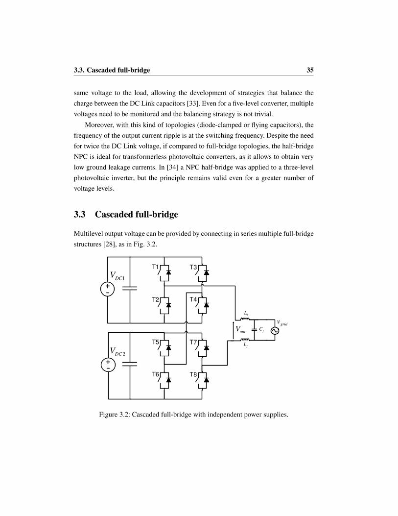
3.3 Cascaded full-bridge
Multilevel output voltage can be provided by connecting in series multiple full-bridge
structures [28], as in Fig. 3.2.
1DCV
2DCV
T1 T3
T2 T4
T5 T7
T6 T8
fL
fL
gridv
fC
outV
Figure 3.2: Cascaded full-bridge with independent power supplies.
36 Chapter 3. State of the art of Multilevel Inverter topologies
Several independent DC sources are needed for the correct operation i.e., multiple
PV strings [35] or transformers followed by diode rectifiers. Another approach is to
employ the transformer not to create the DC supplies but to connect same full-bridge
structures with the same DC supply [36]. Indeed, this represents the major drawback
of this topology [37].
Multiple PWM strategies are available for the cascaded full-bridge: carrier based
modulations [38] or space-vector approaches [39, 40].
Anyway, eight devices are needed, and there are always four devices conducting.
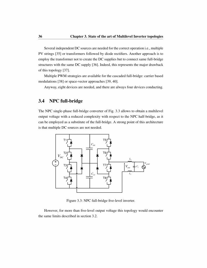
3.4 NPC full-bridge
The NPC single-phase full-bridge converter of Fig. 3.3 allows to obtain a multilevel
output voltage with a reduced complexity with respect to the NPC half-bridge, as it
can be employed as a substitute of the full-bridge. A strong point of this architecture
is that multiple DC sources are not needed.
DCV
HSC
LSC
fL
fL
gridv
fC
outV
T1
T2
T3
T4
T5
T6
T7
T8
Figure 3.3: NPC full-bridge five-level inverter.
However, for more than five-level output voltage this topology would encounter
the same limits described in section 3.2.
3.5. Hybrid five-level topologies 37
3.5 Hybrid five-level topologies
In a hybrid topology, the DC Link voltage is not distributed between multiple struc-
tures. Usually, a simple two level half-bridge is employed to change the polarity of
the output voltage, while a multilevel structure synthesizes the multiple output volt-
age levels. In this way, the devices of the two level half-bridge must sustain the whole
DC Link voltage. Some hybrid topologies for five-level converters were presented in
[41, 42], but only the one presented in [43] (Fig. 3.4) was applied to a photovoltaic
source [44, 45].
In this proposal, a bidirectional switch (realized with an IGBT and four diodes) is
added to a standard full-bridge topology. The additional switch connects the midpoint
of the DC Link to the converter output. The same topology was also extended to a
seven-level output voltage in [46].
HSC
LSC
T1
T2
T3
T4
T5
fL
fL
gridv
fCoutV
DCV
Figure 3.4: Five-level full-bridge topology proposed in [43].

Chapter 4
Novel Nine Level transformerless
Inverter
4.1 Introduction
As described in chapter 3.3, cascaded full-bridge solutions need a separate power
supply for each full-bridge section [47]. The way these supply are generated and the
voltage ratio between them lead to different solutions: [48, 49, 50, 51].
The purpose of this chapter is to describe the development of a nine level cas-
caded full-bridge converter suitable for PV transformerless systems.
4.2 Architecture of the converter
The basic structure is composed of two cascaded full-bridges, the former supplied
by the PV generator and the latter supplied by a flying capacitor. Since there are no
particular constraints on the ratio between the two voltages, for the sake of simplicity
it is assumed that the voltage on the flying capacitor is always lower than the DC
source. For this reason, the PV-fed full-bridge is named High-Voltage Full-Bridge
(HVFB), while the other full-bridge is named Low-Voltage Full-Bridge (LVFB), see
Fig. 4.1.

40 Chapter 4. Novel Nine Level transformerless Inverter
Cascading full-bridge structure is often employed in high-voltage converters, as
the DC Link voltage can be equally divided upon each full-bridge structure, and
devices with lower breakdown voltage requirement can be chosen. However, if the
same DC voltage is chosen for each full-bridge, only a five-level output voltage can
be achieved.
A way to increase the number of voltage levels and to reduce the switching har-
monic distortion is to choose a different voltage for each DC supply. In [52] different
choices are proposed, in particular, if the DC voltage supplies are chosen in a geo-
metric progression of ratio 3, 3n equally-spaced output voltage levels can be achieved
with n full-bridge structures.
If the minimum switching harmonics are pursued, the best choice is to chose the
voltage across the flying capacitor equal to one-third of the DC Link voltage, i.e.,
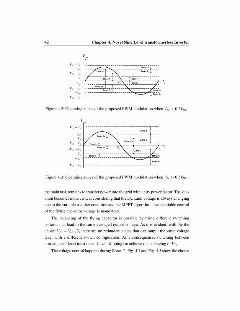
Vf c = VDC/3. With this first approach, different zones can be identified depending
on the output voltage demand: Vout , that represents the average of Vout in a switching
period.
There are several possible ways to provide the same Vout with the available volt-
ages, in this work it was chosen to switch between adjacent voltage levels, to mini-
mize the switching ripple and reduce the switching loss. In this way, the zones of Fig.
4.2 are identified. In the zones identified by the + sign the flying capacitor voltage is
added to the HVFB output, while in the zones identified by the − sign it is subtracted.
Fig. 4.2 is realized under the assumption that Vf c < 0.5VDC, otherwise the levels
are positioned in a different way, see Fig. 4.3 for reference. It is important to note
that the operating zones are the same as the previous case, only the voltage order is
changed. This choice allows to switch between non-adjacent level, and in the follow-
ing it will be explained that this choice has certain benefits.
The PWM strategy is shown in TABLE 4.1. In particular, one leg of the HVFB
commutates at line frequency, while the other presents high-frequency switching be-
havior only in Zone 2, where the flying capacitor voltage is regulated (see section
4.3). Most of the switching is condensed in one leg of the LVFB, while the other
operates at a multiple of the line frequency.
The fact that no high-frequency switching is required in one leg of each full-

4.3. Flying Capacitor Voltage Regulation 41
fL
fC
DCV
fcC
gridv
5T 7T
6T 8T
1T 3T
2T 4T
fcV
outV
High-VoltageFull-Bridge
(HVFB)
Low-VoltageFull-Bridge
(LVFB)
Figure 4.1: Cascaded full-bridge with flying capacitor.
bridge makes possible to employ MOSFETs with a very low on-state resistance, in
order to increase the converter efficiency. In fact, the intrinsic body diode of the power
MOSFET does not offer good dynamic performance, as a trade-off exists between
the on-state resistance and the reverse recovery time. The power IGBTs do not suffer
from this problem, as they do not present an intrinsic body diode, and a high perfor-
mance diode can be embedded in the same package. For this reason, while it is true
that MOSFETs offer low on-state resistance, their application should be avoided for
hard-switching converters.
4.3 Flying Capacitor Voltage Regulation
While the balancing of the flying capacitor in a converter that does not need to transfer
active power, such as shunt active filters, is an easy task, and can be realized by
controlling small amounts of active power [53], this is not the case of a PV inverter.
In fact, although the recent international regulation impose that new designs of
grid-connected inverters must be able to provide specific amount of reactive power,
42 Chapter 4. Novel Nine Level transformerless Inverter
2T T t
Zone 1+
Zone 2+
Zone 2+
outV
DC fcV V+
DC fcV V−
fcV
fcV−
DC fcV V− +
DC fcV V− −
DCV
DCV−
Zone 2-
Zone 2-
Zone 3+
Zone 3-
Zone 3+
Zone 3-
Zone 1-
Figure 4.2: Operating zones of the proposed PWM modulation when Vf c < 0.5VDC.
2T T t
Zone 3+
Zone 3+
Zone 1+
Zone 2+
outV
DC fcV V+
DC fcV V−
fcV
fcV−
DC fcV V− +
DC fcV V− −
DCV
DCV−
Zone 2+
Zone 2-
Zone 2-
Zone 3-
Zone 3-
Zone 1-
Figure 4.3: Operating zones of the proposed PWM modulation when Vf c > 0.5VDC.
the main task remains to transfer power into the grid with unity power factor. The situ-
ation becomes more critical considering that the DC Link voltage is always changing
due to the variable weather condition and the MPPT algorithm, thus a reliable control
of the flying capacitor voltage is mandatory.
The balancing of the flying capacitor is possible by using different switching
patterns that lead to the same averaged output voltage. As it is evident, with the the
choice Vf c = VDC/3, there are no redundant states that can output the same voltage
level with a different switch configuration. As a consequence, switching between
non-adjacent level must occur (level skipping) to achieve the balancing of Vf c.
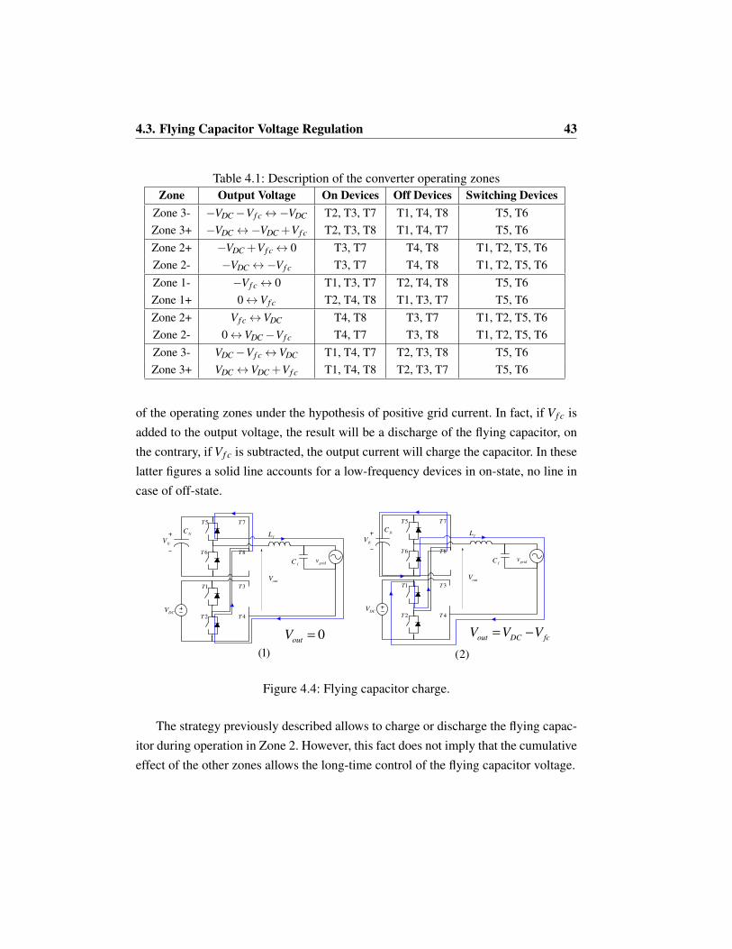
The voltage control happens during Zones 2. Fig. 4.4 and Fig. 4.5 show the choice
4.3. Flying Capacitor Voltage Regulation 43
Table 4.1: Description of the converter operating zones
Zone Output Voltage On Devices Off Devices Switching Devices
Zone 3- −VDC −Vf c ↔−VDC T2, T3, T7 T1, T4, T8 T5, T6
Zone 3+ −VDC ↔−VDC +Vf c T2, T3, T8 T1, T4, T7 T5, T6
Zone 2+ −VDC +Vf c ↔ 0 T3, T7 T4, T8 T1, T2, T5, T6
Zone 2- −VDC ↔−Vf c T3, T7 T4, T8 T1, T2, T5, T6
Zone 1- −Vf c ↔ 0 T1, T3, T7 T2, T4, T8 T5, T6
Zone 1+ 0 ↔Vf c T2, T4, T8 T1, T3, T7 T5, T6
Zone 2+ Vf c ↔VDC T4, T8 T3, T7 T1, T2, T5, T6
Zone 2- 0 ↔VDC −Vf c T4, T7 T3, T8 T1, T2, T5, T6
Zone 3- VDC −Vf c ↔VDC T1, T4, T7 T2, T3, T8 T5, T6
Zone 3+ VDC ↔VDC +Vf c T1, T4, T8 T2, T3, T7 T5, T6
of the operating zones under the hypothesis of positive grid current. In fact, if Vf c is
added to the output voltage, the result will be a discharge of the flying capacitor, on
the contrary, if Vf c is subtracted, the output current will charge the capacitor. In these
latter figures a solid line accounts for a low-frequency devices in on-state, no line in
case of off-state.
fL
fC
DCV
fcC
gridv
5T 7T
6T 8T
1T 3T
2T 4T
fcV
outV
(1)
0out
V =
fL
fC
DCV
fcC
gridv
5T 7T
6T 8T
1T 3T
2T 4T
fcV
outV
(2)
out DC fcV V V= −
Figure 4.4: Flying capacitor charge.
The strategy previously described allows to charge or discharge the flying capac-
itor during operation in Zone 2. However, this fact does not imply that the cumulative
effect of the other zones allows the long-time control of the flying capacitor voltage.
44 Chapter 4. Novel Nine Level transformerless Inverter
fL
fC
DCV
fcC
gridv
5T 7T
6T 8T
1T 3T
2T 4T
fcV
outV
out fcV V=
fL
fC
DCV
fcC
gridv
5T 7T
6T 8T
1T 3T
2T 4T
fcV
outV
out DCV V=
(1) (2)
Figure 4.5: Flying capacitor discharge.
To this aim, extensive simulations regarding the theoretical behavior of the power
converter operating under different supply voltage conditions were performed. De-
pending on the operating zone and on the current magnitude, the average current
charging the flying capacitor during a grid voltage period can be evaluated. In the
following analysis a sinusoidal voltage of amplitude vgrid = 230√
2 was considered.
A voltage sweep of both the DC Link and flying capacitor voltages was performed
and the average current of the flying capacitor was evaluated in the following cases:
1. The configurations that lead to a charge of the flying capacitor (Fig. 4.4) are
always chosen, and the average charging current I+f c is evaluated.
2. The configurations that lead to a discharge of the flying capacitor (Fig. 4.5) are
always chosen and the average charging current I−f c is evaluated.
If I+f c is positive and I−f c is negative it means that with the combination (VDC,Vf c)
the flying capacitor voltage is fully controllable. Otherwise it can happen I+f c < 0
(the flying capacitor cannot be charged) or I−f c > 0 (the flying capacitor cannot be
discharged). As I+f c > I−f c, the cases above cover all the possibilities.
It is important to note that the magnitude of the grid current is not important, as it
affects only the absolute value of I+f c and I−f c and not the sign. Moreover, the analysis
is based on the duty cycles, so the results hold for every pair (VDC/vgrid ,Vf c/vgrid).
Fig. 4.6 reports the results of the simulations. Only the points where VDC > Vf c

4.3. Flying Capacitor Voltage Regulation 45
(as hypothesized) and VDC +Vf c > vgrid (the converter can control the grid current)
are significant.
The white area delimited by the bottom and right edges of the plot and the grey
area represents the condition of full controllability of Vf c, the black area represents
the condition I−f c > 0 and the grey area I+f c < 0. For this set of simulations a sinusoidal
grid current with unity power factor was considered.
VDC
[V]
Vfc
[V
]
Unity Power Factor
200 250 300 350 400 450 500 550 60050
100
150
200
250
300
350
400
Figure 4.6: Flying capacitor control behavior with unity power factor.
From the results of Fig. 4.6 these consideration can be done:
• If the converter enters the black area, Vf c will rapidly rise (the point of opera-
tion will move upwards in the graph) until entering the white area.
• If the converter enters the grey area, Vf c will decrease (the point of operation
will move downwards in the graph) until entering the white area.
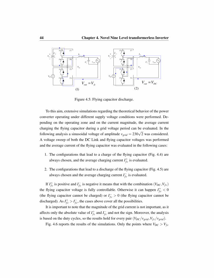
46 Chapter 4. Novel Nine Level transformerless Inverter
VDC
[V]
Vfc
[V
]
Power Factor: 0.70
200 250 300 350 400 450 500 550 60050
100
150
200
250
300
350
400
VDC
[V]
Vfc
[V
]
Power Factor: 0.50
200 250 300 350 400 450 500 550 60050
100
150
200
250
300
350
400
Figure 4.7: Flying capacitor control behavior with different values of power factor.
• Even if the balancing control fails, Vf c is limited by the grey area.
• The white area between the black and the grey one represents a stable operating
condition of the converter.
4.4 Application to transformerless photovoltaic converters
A peculiar characteristic of the modulation strategy is that particular care must be
taken when commutating T3 and T4. In fact, the leg formed by T3 and T4 is directly
connected to the neutral conductor. This means that during the commutation high cur-
rents will circulate in the neutral conductor due to the panels’ parasitic capacitance.
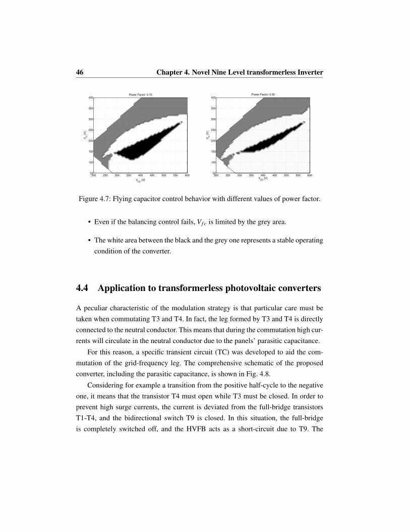
For this reason, a specific transient circuit (TC) was developed to aid the com-
mutation of the grid-frequency leg. The comprehensive schematic of the proposed
converter, including the parasitic capacitance, is shown in Fig. 4.8.
Considering for example a transition from the positive half-cycle to the negative
one, it means that the transistor T4 must open while T3 must be closed. In order to
prevent high surge currents, the current is deviated from the full-bridge transistors
T1-T4, and the bidirectional switch T9 is closed. In this situation, the full-bridge
is completely switched off, and the HVFB acts as a short-circuit due to T9. The

4.4. Application to transformerless photovoltaic converters 47
fL
fC
DCV
fcC
gridv
5T 7T
6T 8T
1T 3T
2T 4T
1M
2M
TR
9T
pC
fcV
groundv
Figure 4.8: Proposed topology.
potential of the parasitic capacitor remains floating, and is still at the previous value
vground = 0V .
Then, the low-power MOSFET M1 is switched on, charging with a first order
transient the parasitic capacitance Cp through the resistance RT , see Fig. 4.9 and Fig.
4.10.
When the transient ends, it is safe to switch on the transistors T4 and T2 and to
switch off the bidirectional switch T9.
In other words, the parasitic capacitance is always charged through RT , and the
current peaks are acceptable. This can be done because while the HVFB supplies the
zero voltage, the current can be controlled with the switching of the LVFB.
The power loss of the transient circuit can be evaluated with the well-known for-
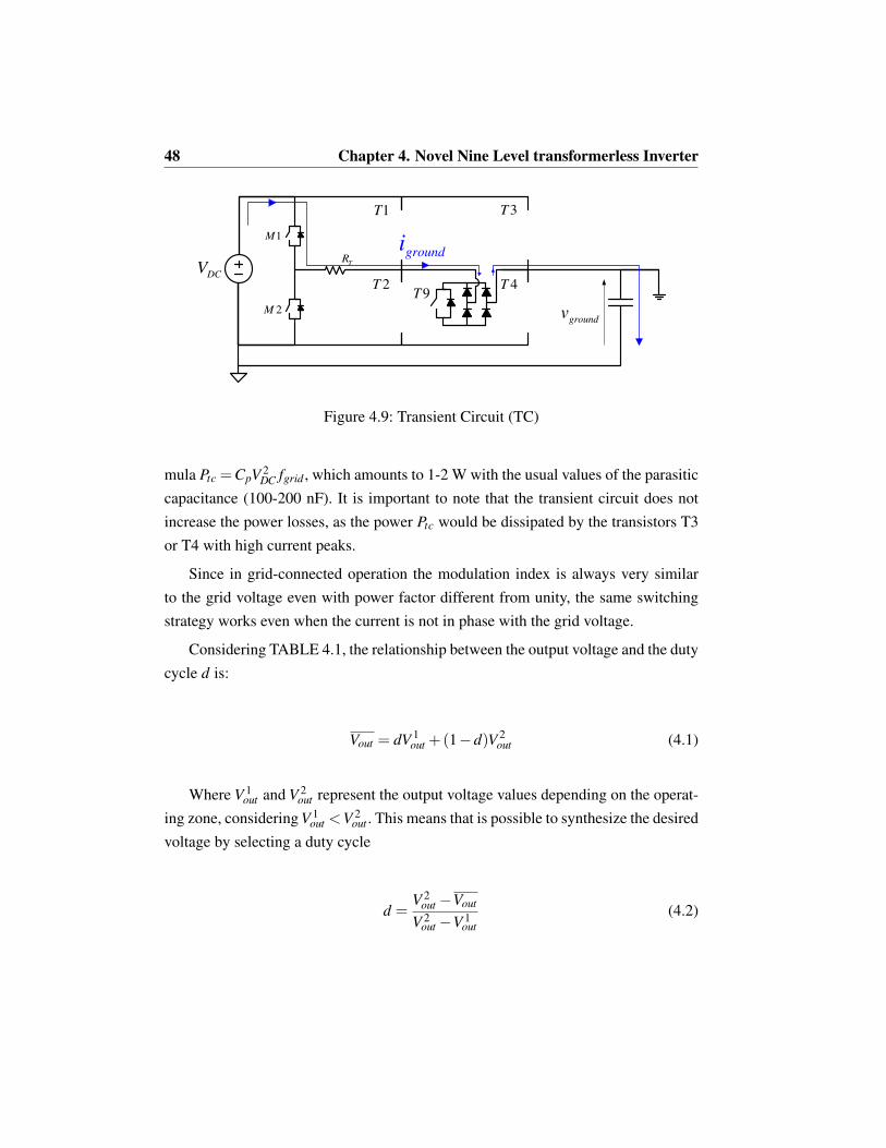
48 Chapter 4. Novel Nine Level transformerless Inverter
DCV
1T 3T
2T 4T
1M
2M
TR
9T
groundv
groundi
Figure 4.9: Transient Circuit (TC)
mula Ptc =CpV 2DC fgrid , which amounts to 1-2 W with the usual values of the parasitic
capacitance (100-200 nF). It is important to note that the transient circuit does not
increase the power losses, as the power Ptc would be dissipated by the transistors T3
or T4 with high current peaks.
Since in grid-connected operation the modulation index is always very similar
to the grid voltage even with power factor different from unity, the same switching
strategy works even when the current is not in phase with the grid voltage.
Considering TABLE 4.1, the relationship between the output voltage and the duty
cycle d is:
Vout = dV 1out +(1−d)V 2
out (4.1)
Where V 1out and V 2
out represent the output voltage values depending on the operat-
ing zone, considering V 1out <V 2
out . This means that is possible to synthesize the desired
voltage by selecting a duty cycle
d =V 2
out −Vout
V 2out −V 1
out
(4.2)

4.5. DC Voltage independent modulation 49
Gro
und c
urr
ent i
gro
un
d
Gro
und v
oltage v g
rou
nd
VDC
/RT
VDC
Figure 4.10: Transient Circuit example waveforms.
4.5 DC Voltage independent modulation
As the DC Link voltage changes due to the variability of the solar irradiance, the
operation of the converter must not be affected. In fact, it is easy to derive the duty
cycles in case of fixed voltage ratio between VDC and Vf c, otherwise the computation
has to be done on-line.
This kind of approach employs the measurement of the DC voltage in order to
synthesize, in the next PWM cycle, the desired value. The on-line calculation of the
duty cycle was already explored in [40], and in this thesis it is customized to the
modulation strategy.
4.6 Simulation Results
Extensive simulation results concerning grid current distortion and ground leakage
current were performed in order to highlight the characteristic of the proposed con-
verter and modulation strategy.
The tool employed for the simulation was the PLECS toolbox in a Simulink en-
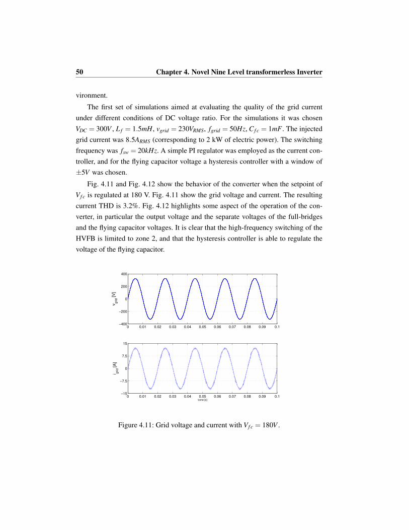
50 Chapter 4. Novel Nine Level transformerless Inverter
vironment.
The first set of simulations aimed at evaluating the quality of the grid current
under different conditions of DC voltage ratio. For the simulations it was chosen
VDC = 300V , L f = 1.5mH, vgrid = 230VRMS, fgrid = 50Hz, C f c = 1mF . The injected
grid current was 8.5ARMS (corresponding to 2 kW of electric power). The switching
frequency was fsw = 20kHz. A simple PI regulator was employed as the current con-
troller, and for the flying capacitor voltage a hysteresis controller with a window of
±5V was chosen.
Fig. 4.11 and Fig. 4.12 show the behavior of the converter when the setpoint of
Vf c is regulated at 180 V. Fig. 4.11 show the grid voltage and current. The resulting
current THD is 3.2%. Fig. 4.12 highlights some aspect of the operation of the con-
verter, in particular the output voltage and the separate voltages of the full-bridges
and the flying capacitor voltages. It is clear that the high-frequency switching of the
HVFB is limited to zone 2, and that the hysteresis controller is able to regulate the
voltage of the flying capacitor.
0 0.01 0.02 0.03 0.04 0.05 0.06 0.07 0.08 0.09 0.1−400
−200
0
200
400
vgrid [
V]
0 0.01 0.02 0.03 0.04 0.05 0.06 0.07 0.08 0.09 0.1−15
−7.5
0
7.5
15
tome [s]
i grid [
A]
Figure 4.11: Grid voltage and current with Vf c = 180V .

4.6. Simulation Results 51
0 0.01 0.02 0.03 0.04 0.05 0.06 0.07 0.08 0.09 0.1−500
0
500
Vout [
V]
0 0.01 0.02 0.03 0.04 0.05 0.06 0.07 0.08 0.09 0.1−500
0
500
HV
FB
and L
VF
Boutp
ut voltages
0 0.01 0.02 0.03 0.04 0.05 0.06 0.07 0.08 0.09 0.1170
180
190
time [s]
Vfc
[V
]
HVFB
LVFB
Figure 4.12: Converter output voltage, HVFB and LVFB output voltages and Flying
capacitor voltage with Vf c = 180V .
In the following simulations, the same waveforms of Fig. 4.11 and Fig. 4.12 are
reported for different values of Vf c. It is important to note that the THD gradually
decreases with the flying capacitor voltage, due to the reduced output voltage ripple.
In fact, with Vf c = 150V (Fig. 4.13 and Fig. 4.14) the THD is 2.9%, while with
Vf c = 100V (Fig. 4.15 and Fig. 4.16) the THD is 2.6%.
During these simulations only a first order filter and a rather low switching fre-
quency were employed. In fact, the THD could be further reduced by modifying these
two design parameters.
The performance of the proposed modulation strategy and TC were evaluated
by simulating the PV parasitic capacitor with a capacitance connected between the
neutral conductor and the negative side of the DC Link. It is worth noting that the
parasitic capacitance is distributed between the positive and negative poles of the DC
Link, but it is irrelevant to the analysis, as in the equivalent common mode circuit the
DC Link is short-circuited.
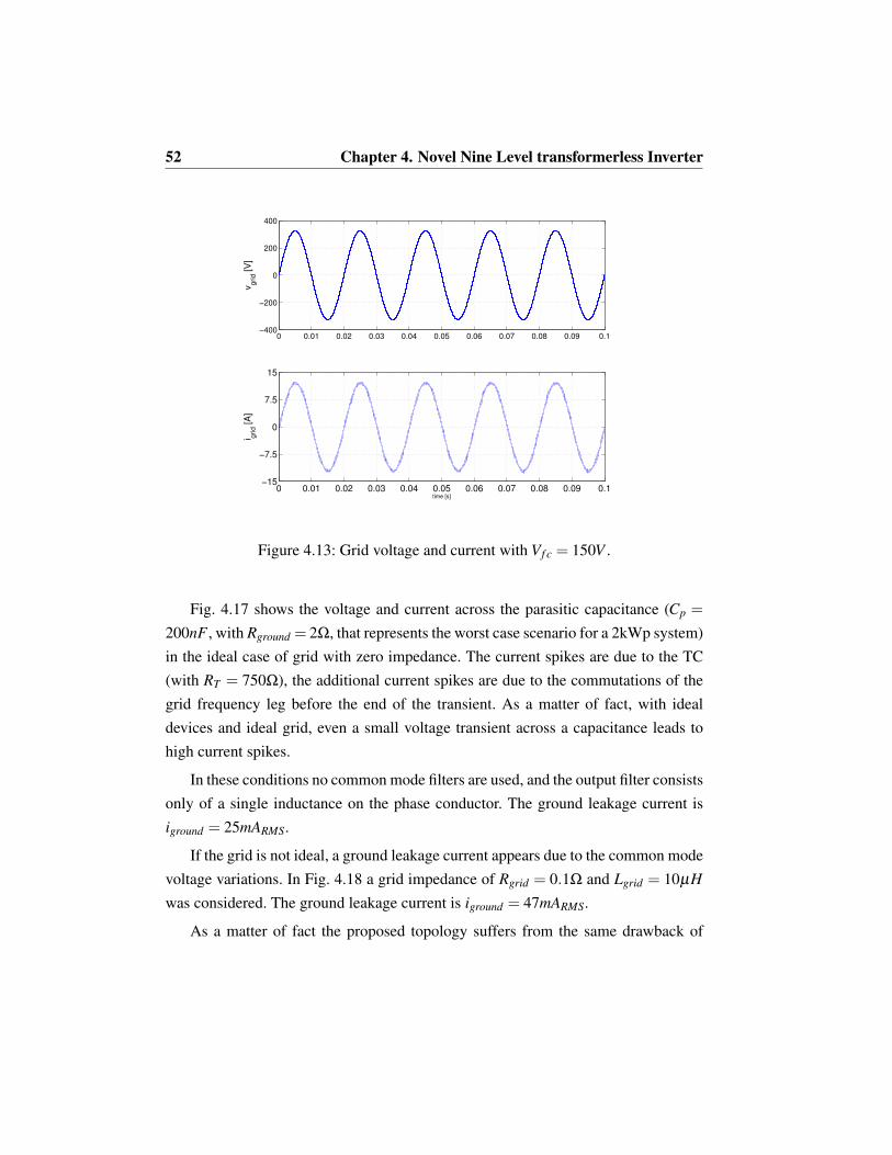
52 Chapter 4. Novel Nine Level transformerless Inverter
0 0.01 0.02 0.03 0.04 0.05 0.06 0.07 0.08 0.09 0.1−15
−7.5
0
7.5
15
time [s]
i grid [
A]
0 0.01 0.02 0.03 0.04 0.05 0.06 0.07 0.08 0.09 0.1−400
−200
0
200
400
vgrid [
V]
Figure 4.13: Grid voltage and current with Vf c = 150V .
Fig. 4.17 shows the voltage and current across the parasitic capacitance (Cp =
200nF , with Rground = 2Ω, that represents the worst case scenario for a 2kWp system)
in the ideal case of grid with zero impedance. The current spikes are due to the TC
(with RT = 750Ω), the additional current spikes are due to the commutations of the
grid frequency leg before the end of the transient. As a matter of fact, with ideal
devices and ideal grid, even a small voltage transient across a capacitance leads to
high current spikes.
In these conditions no common mode filters are used, and the output filter consists
only of a single inductance on the phase conductor. The ground leakage current is
iground = 25mARMS.
If the grid is not ideal, a ground leakage current appears due to the common mode
voltage variations. In Fig. 4.18 a grid impedance of Rgrid = 0.1Ω and Lgrid = 10µH
was considered. The ground leakage current is iground = 47mARMS.
As a matter of fact the proposed topology suffers from the same drawback of
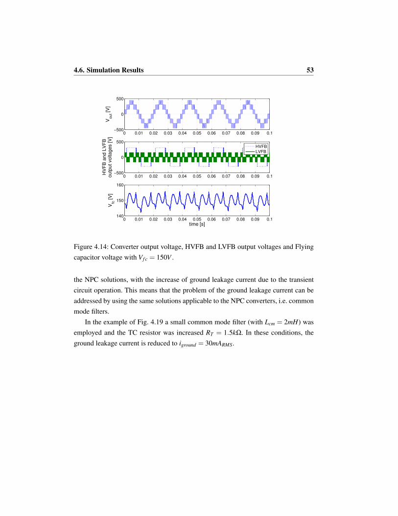
4.6. Simulation Results 53
0 0.01 0.02 0.03 0.04 0.05 0.06 0.07 0.08 0.09 0.1−500
0
500
Vout [
V]
0 0.01 0.02 0.03 0.04 0.05 0.06 0.07 0.08 0.09 0.1−500
0
500
HV
FB
and L
VF
Boutp
ut voltages [V
]
0 0.01 0.02 0.03 0.04 0.05 0.06 0.07 0.08 0.09 0.1140
150
160
time [s]
Vfc
[V
]
HVFB
LVFB
Figure 4.14: Converter output voltage, HVFB and LVFB output voltages and Flying
capacitor voltage with Vf c = 150V .
the NPC solutions, with the increase of ground leakage current due to the transient
circuit operation. This means that the problem of the ground leakage current can be
addressed by using the same solutions applicable to the NPC converters, i.e. common
mode filters.
In the example of Fig. 4.19 a small common mode filter (with Lcm = 2mH) was
employed and the TC resistor was increased RT = 1.5kΩ. In these conditions, the
ground leakage current is reduced to iground = 30mARMS.
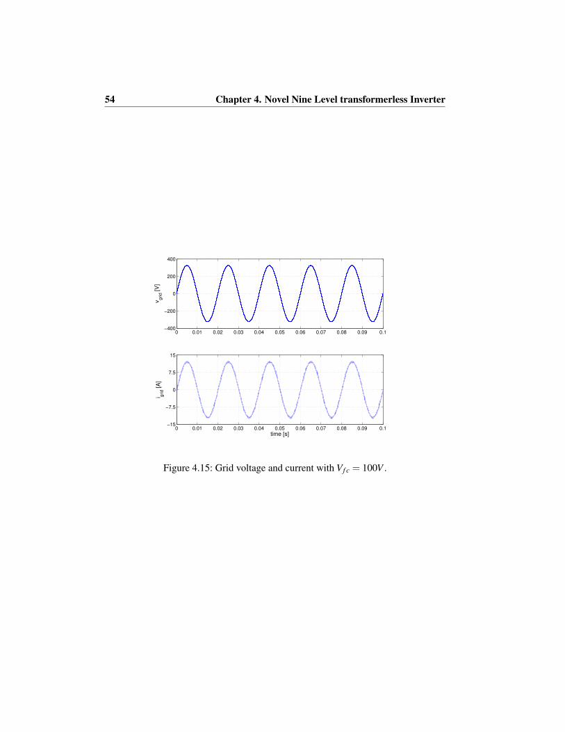
54 Chapter 4. Novel Nine Level transformerless Inverter
0 0.01 0.02 0.03 0.04 0.05 0.06 0.07 0.08 0.09 0.1−400
−200
0
200
400
vgrid [
V]
0 0.01 0.02 0.03 0.04 0.05 0.06 0.07 0.08 0.09 0.1−15
−7.5
0
7.5
15
time [s]
i grid [
A]
Figure 4.15: Grid voltage and current with Vf c = 100V .

4.6. Simulation Results 55
0 0.01 0.02 0.03 0.04 0.05 0.06 0.07 0.08 0.09 0.1−500
0
500
Vout [
V]
0 0.01 0.02 0.03 0.04 0.05 0.06 0.07 0.08 0.09 0.1−500
0
500
HV
FB
and L
VF
Boutp
ut voltages [V
]
0 0.01 0.02 0.03 0.04 0.05 0.06 0.07 0.08 0.09 0.190
100
110
120
time [s]
Vfc
[V
]
HVFB
LVFB
Figure 4.16: Converter output voltage, HVFB and LVFB output voltages and Flying
capacitor voltage with Vf c = 100V .
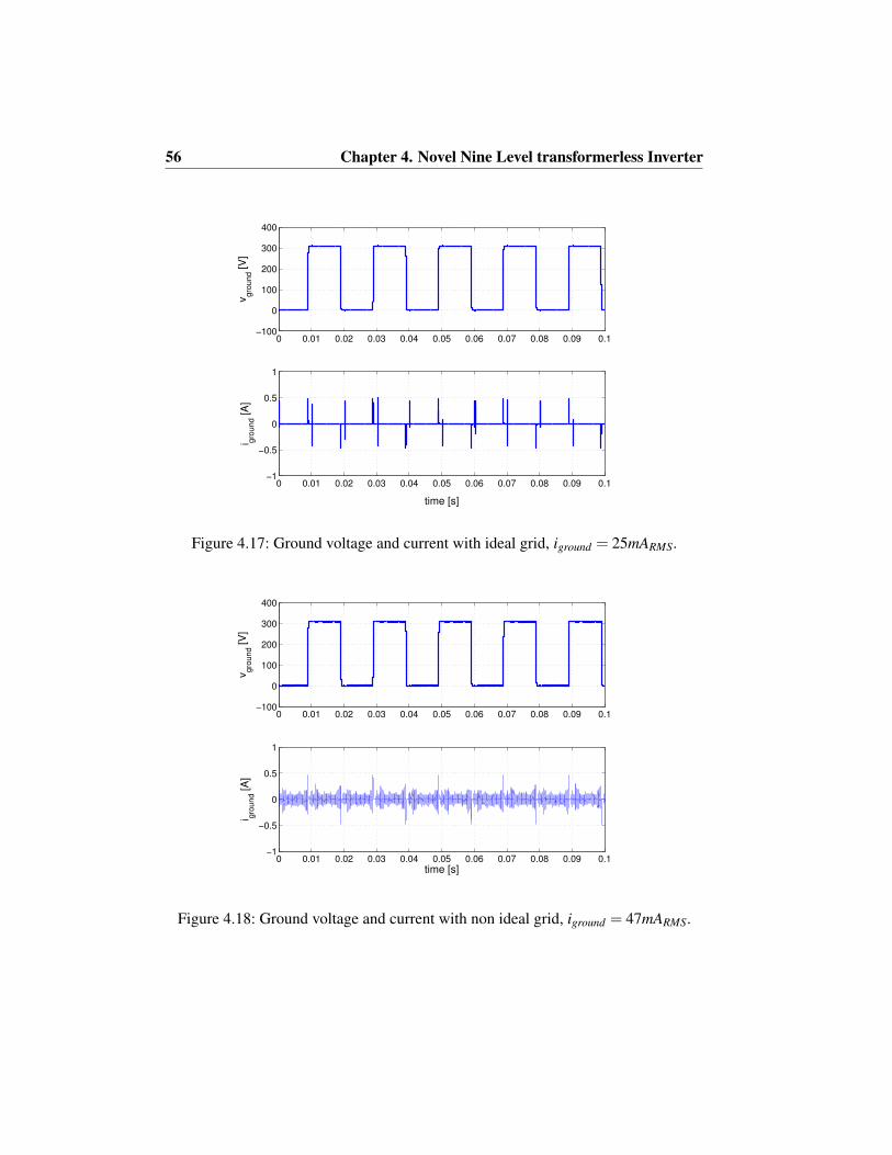
56 Chapter 4. Novel Nine Level transformerless Inverter
0 0.01 0.02 0.03 0.04 0.05 0.06 0.07 0.08 0.09 0.1−100
0
100
200
300
400
vg
rou
nd [
V]
0 0.01 0.02 0.03 0.04 0.05 0.06 0.07 0.08 0.09 0.1−1
−0.5
0
0.5
1
time [s]
i gro
un
d [
A]
Figure 4.17: Ground voltage and current with ideal grid, iground = 25mARMS.
0 0.01 0.02 0.03 0.04 0.05 0.06 0.07 0.08 0.09 0.1−100
0
100
200
300
400
vg
rou
nd [
V]
0 0.01 0.02 0.03 0.04 0.05 0.06 0.07 0.08 0.09 0.1−1
−0.5
0
0.5
1
time [s]
i gro
un
d [
A]
Figure 4.18: Ground voltage and current with non ideal grid, iground = 47mARMS.
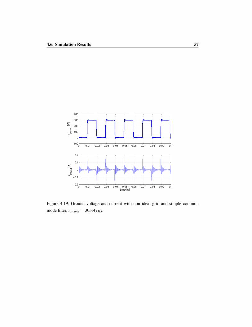
4.6. Simulation Results 57
0 0.01 0.02 0.03 0.04 0.05 0.06 0.07 0.08 0.09 0.1−100
0
100
200
300
400
vg
rou
nd [
V]
0 0.01 0.02 0.03 0.04 0.05 0.06 0.07 0.08 0.09 0.1−0.2
−0.1
0
0.1
0.2
time [s]
i gro
un
d [
A]
Figure 4.19: Ground voltage and current with non ideal grid and simple common
mode filter, iground = 30mARMS.
58 Chapter 4. Novel Nine Level transformerless Inverter
4.7 Nine Level converter prototype
In order to test the proposed converter, a prototype was designed and built. The proto-
type must be completely stand-alone, it includes the CPU, that implements the control
and the modulation, both full-bridges and the transient circuit, the sensors, the power
supply for the logic and analog circuits and the output filter. Due to the complexity of
the design and the number of components involved, three boards were designed: the
control board, the power board and the output stage board.
4.7.1 Control board
The control board is a daughter board for the Power one. It was designed to fit in a
DIM100 socket in order to change the CPU without redesigning the power circuits.
The control board embeds the DSC TMS320F28335, a 150MHz, 32bit processor by
Texas Instruments. The high number of PWM channels (12) and Analog to Digital
Converter Channels (16) along with the floating point unit make it possible to imple-
ment complex algorithms.
Along with the CPU, the control board embeds the voltage regulator (3.3V for
the peripherals and 1.9V for the core) and the protection circuit for the ADC.
The complete schematic and PCB are found in Appendices A1.1 and A1.2.
4.7.2 Power board
The power board incorporates the active devices, the DC Links, the driving circuits
and the DSP socket with I/O circuitry.
DSP Socket
The Power card embeds the DSP socket with additional I/O circuits. The socket con-
veys to the DSP the analog signals, the 5V power supply and the various I/O and
PWM ports that operate the converter.
As I/O interfaces, the Power board embeds a 10 bit Digital to Analog Converter
(DAC) TLV5631, a RS485 transciever SN75LBC182D and various general purpose

4.7. Nine Level converter prototype 59
connectors. The complete schematic is found in appendix A1.3.
Gate drivers
In order to have a very flexible control on every power device, the gate driver circuit
is composed of an optocoupler and an insulated power supply for every power device.
The chosen optocoupler is the Allegro ACPL-J313. The insulated power supply
is generated by the IC MAX256 that drives a 1:2 transformer followed by a voltage
multiplier. The schematic is illustrated in Fig. 4.20. The PWM signal is generated
by the DSP and it enters in a AND gate with the signal generated by the fault cir-
cuit. The fault circuit is a latch that, in case of overcurrent, forces to zero its output,
consequently disabling all the logic gates.
1:2
5V
L78L15220nF
1µF
15V
5V
PWM
FAULTn
ENABLE
Figure 4.20: Gate driver circuit with insulated power supply.
The logic gates are in open drain configuration. In this way the current absorbed
by the photodiodes is given by the 5V power supply and not by the logic gates itself.
This, however, poses a problem in case of malfunctioning or non-uniform turn on of
the devices. As a matter of fact, if the logic gate is not powered, every photodiode
is conducting due to the pull-up resistor. For this reason, every cathode of the gate
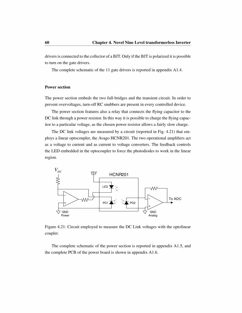
60 Chapter 4. Novel Nine Level transformerless Inverter
drivers is connected to the collector of a BJT. Only if the BJT is polarized it is possible
to turn on the gate drivers.
The complete schematic of the 11 gate drivers is reported in appendix A1.4.
Power section
The power section embeds the two full-bridges and the transient circuit. In order to
prevent overvoltages, turn-off RC snubbers are present in every controlled device.
The power section features also a relay that connects the flying capacitor to the
DC link through a power resistor. In this way it is possible to charge the flying capac-
itor to a particular voltage, as the chosen power resistor allows a fairly slow charge.
The DC link voltages are measured by a circuit (reported in Fig. 4.21) that em-
ploys a linear optocoupler, the Avago HCNR201. The two operational amplifiers act
as a voltage to current and as current to voltage converters. The feedback controls
the LED embedded in the optocoupler to force the photodiodes to work in the linear
region.
LED
PD1 PD2
HCNR20115VDC
V
GNDPower
GNDAnalog
To ADC
Figure 4.21: Circuit employed to measure the DC Link voltages with the optolinear
coupler.
The complete schematic of the power section is reported in appendix A1.5, and
the complete PCB of the power board is shown in appendix A1.6.

4.7. Nine Level converter prototype 61
4.7.3 Output Stage Board
Power supply
In order to generate all the supply voltages needed for the converter, a flyback based
on the IC TOP257-PN was designed. Fig. 4.22 shows an example of the general
flyback circuit. The controller incorporates an active switch used to drive the primary
of the transformer. The DC supply is obtained by a simple diode bridge rectifier,
allowing it to be used with DC or AC sources.
An optocoupler carries the feedback signal of the controlled output voltage (5V)
to the TOP257-PN.
Figure 4.22: Example circuit of the flyback converter from the TOP257-PN datasheet.
Appendix A1.7 shows the complete shcematic of the realized flyback converter.
Along with the regulated 5V, additional windings for the +17V and -17V (used by the
analog circuits) were added to the design. Also an auxiliary winding for the operation
of the TOP257-PN and an isolated +15V are present. It is important to note that the
5V is the only output regulated by the flyback controller, the other outputs can vary
their voltage depending on the duty cycle variations of the IC due to varying load.
For this reason, to ensure the stability of the power supplies, the unregulated outputs
are followed by linear regulators.
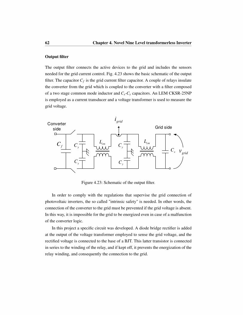
62 Chapter 4. Novel Nine Level transformerless Inverter
Output filter
The output filter connects the active devices to the grid and includes the sensors
needed for the grid current control. Fig. 4.23 shows the basic schematic of the output
filter. The capacitor C f is the grid current filter capacitor. A couple of relays insulate
the converter from the grid which is coupled to the converter with a filter composed
of a two stage common mode inductor and Cx-Cy capacitors. An LEM CKSR-25NP
is employed as a current transducer and a voltage transformer is used to measure the
grid voltage.
xC
yC
yC
yC
yC
fC cmL cm
L
Converter
side Grid side
gridi
gridv
Figure 4.23: Schematic of the output filter.
In order to comply with the regulations that supervise the grid connection of
photovoltaic inverters, the so called "intrinsic safety" is needed. In other words, the
connection of the converter to the grid must be prevented if the grid voltage is absent.
In this way, it is impossible for the grid to be energized even in case of a malfunction
of the converter logic.
In this project a specific circuit was developed. A diode bridge rectifier is added
at the output of the voltage transformer employed to sense the grid voltage, and the
rectified voltage is connected to the base of a BJT. This latter transistor is connected
in series to the winding of the relay, and if kept off, it prevents the energization of the
relay winding, and consequently the connection to the grid.
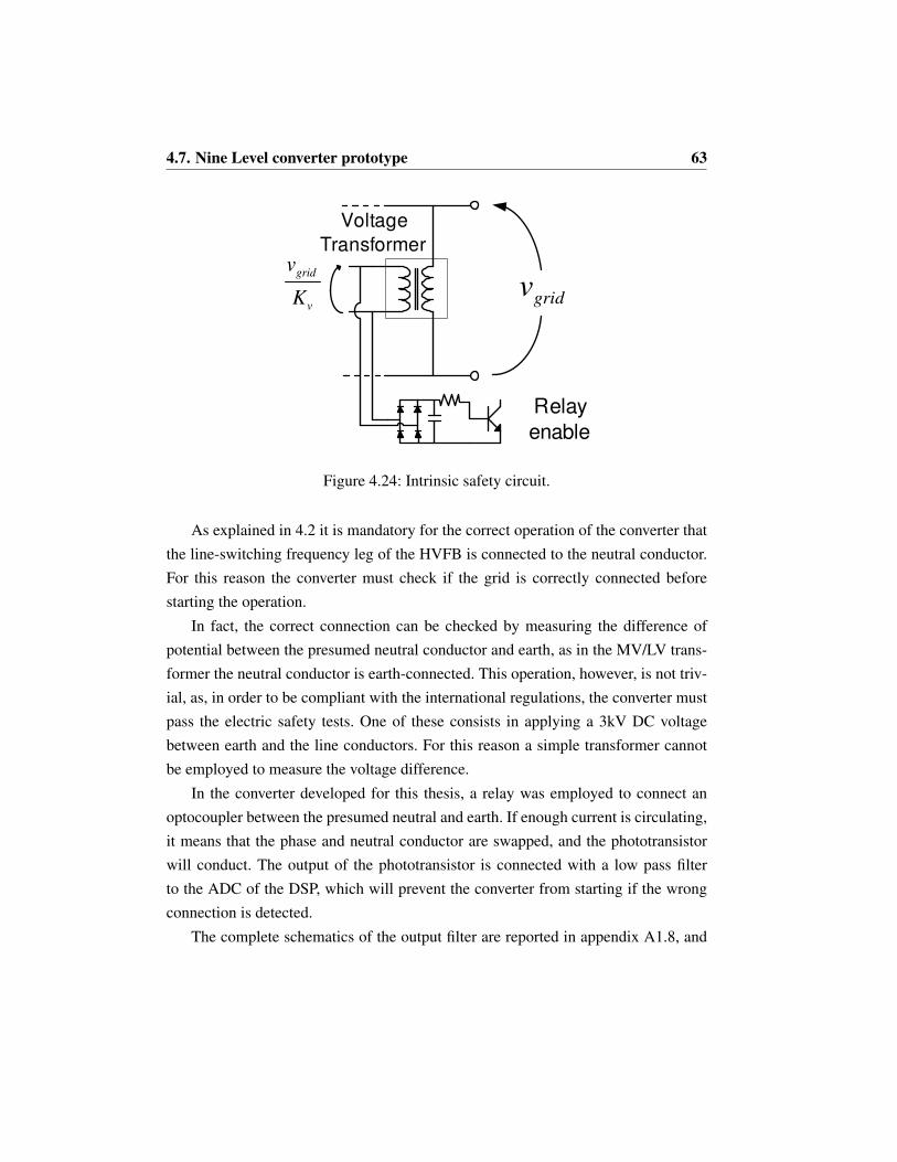
4.7. Nine Level converter prototype 63
gridv
grid
v
v
K
Relay
enable
Voltage
Transformer
Figure 4.24: Intrinsic safety circuit.
As explained in 4.2 it is mandatory for the correct operation of the converter that
the line-switching frequency leg of the HVFB is connected to the neutral conductor.
For this reason the converter must check if the grid is correctly connected before
starting the operation.
In fact, the correct connection can be checked by measuring the difference of
potential between the presumed neutral conductor and earth, as in the MV/LV trans-
former the neutral conductor is earth-connected. This operation, however, is not triv-
ial, as, in order to be compliant with the international regulations, the converter must
pass the electric safety tests. One of these consists in applying a 3kV DC voltage
between earth and the line conductors. For this reason a simple transformer cannot
be employed to measure the voltage difference.
In the converter developed for this thesis, a relay was employed to connect an
optocoupler between the presumed neutral and earth. If enough current is circulating,
it means that the phase and neutral conductor are swapped, and the phototransistor
will conduct. The output of the phototransistor is connected with a low pass filter
to the ADC of the DSP, which will prevent the converter from starting if the wrong
connection is detected.
The complete schematics of the output filter are reported in appendix A1.8, and
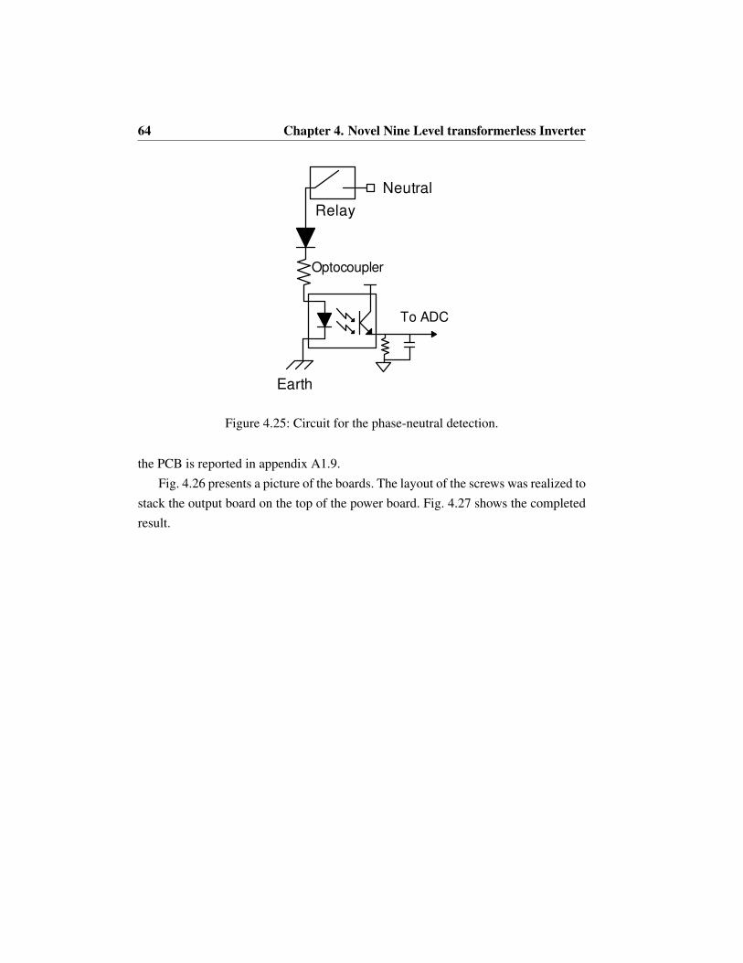
64 Chapter 4. Novel Nine Level transformerless Inverter
Earth
Neutral
Relay
Optocoupler
To ADC
Figure 4.25: Circuit for the phase-neutral detection.
the PCB is reported in appendix A1.9.
Fig. 4.26 presents a picture of the boards. The layout of the screws was realized to
stack the output board on the top of the power board. Fig. 4.27 shows the completed
result.

4.7. Nine Level converter prototype 65
Figure 4.26: Picture of the prototype with the boards separated.
Figure 4.27: Picture of the prototype with the stacked boards.
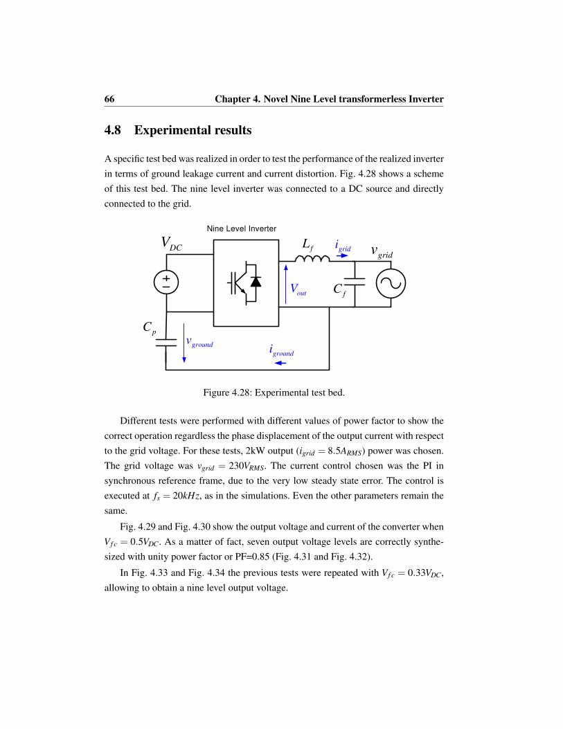
66 Chapter 4. Novel Nine Level transformerless Inverter
4.8 Experimental results
A specific test bed was realized in order to test the performance of the realized inverter
in terms of ground leakage current and current distortion. Fig. 4.28 shows a scheme
of this test bed. The nine level inverter was connected to a DC source and directly
connected to the grid.
gridv
pC
fLDCV
groundigroundv
outV
gridi
Nine Level Inverter
fC
Figure 4.28: Experimental test bed.
Different tests were performed with different values of power factor to show the
correct operation regardless the phase displacement of the output current with respect
to the grid voltage. For these tests, 2kW output (igrid = 8.5ARMS) power was chosen.
The grid voltage was vgrid = 230VRMS. The current control chosen was the PI in
synchronous reference frame, due to the very low steady state error. The control is
executed at fs = 20kHz, as in the simulations. Even the other parameters remain the
same.
Fig. 4.29 and Fig. 4.30 show the output voltage and current of the converter when
Vf c = 0.5VDC. As a matter of fact, seven output voltage levels are correctly synthe-
sized with unity power factor or PF=0.85 (Fig. 4.31 and Fig. 4.32).
In Fig. 4.33 and Fig. 4.34 the previous tests were repeated with Vf c = 0.33VDC,
allowing to obtain a nine level output voltage.

4.8. Experimental results 67
Figure 4.29: Converter output voltage and current with Vf c = 0.5VDC and unity power
factor.
Nine level output voltages can also be realized when Vf c = 0.66VDC. Fig. 4.35,
4.36, 4.37, 4.38 show the behavior of the converter with different power factors.
From the analysis of the experimental results, it is clear that the balancing mech-
anism of the DC voltages allows to control very well the flying capacitor voltage.
Also several points of the controllability area of Fig. 4.6 were experimentally tested.
A very good agreement of the simulations and the experiments was witnessed, al-
though differences appear due to the distortion in the grid voltage.
The distortion of the grid voltage, that is clear in the above oscilloscope captures,
is one of the main causes of the grid current distortion. In fact, the d-q current con-
trol presents infinite gain only at the grid frequency. As the grid voltage presents a
marked third harmonic content, low frequency oscillation happens due to the finite
bandwidth.
Moreover, it can be said that the current distortion when Vf c = 0.33VDC is greater
than the case when Vf c = 0.66VDC. This is due to the effect of the dead times between
the commutation of the full-bridge legs. As it was shown in literature, narrow pulses
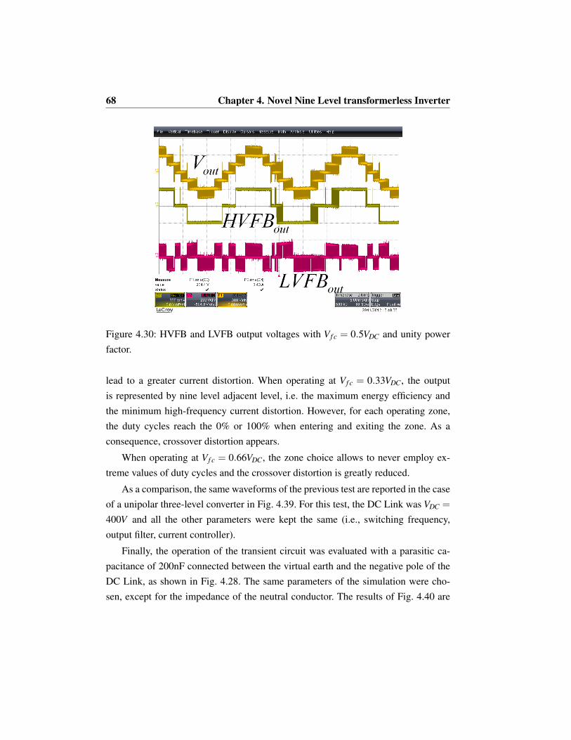
68 Chapter 4. Novel Nine Level transformerless Inverter
Figure 4.30: HVFB and LVFB output voltages with Vf c = 0.5VDC and unity power
factor.
lead to a greater current distortion. When operating at Vf c = 0.33VDC, the output
is represented by nine level adjacent level, i.e. the maximum energy efficiency and
the minimum high-frequency current distortion. However, for each operating zone,
the duty cycles reach the 0% or 100% when entering and exiting the zone. As a
consequence, crossover distortion appears.
When operating at Vf c = 0.66VDC, the zone choice allows to never employ ex-
treme values of duty cycles and the crossover distortion is greatly reduced.
As a comparison, the same waveforms of the previous test are reported in the case
of a unipolar three-level converter in Fig. 4.39. For this test, the DC Link was VDC =
400V and all the other parameters were kept the same (i.e., switching frequency,
output filter, current controller).
Finally, the operation of the transient circuit was evaluated with a parasitic ca-
pacitance of 200nF connected between the virtual earth and the negative pole of the
DC Link, as shown in Fig. 4.28. The same parameters of the simulation were cho-
sen, except for the impedance of the neutral conductor. The results of Fig. 4.40 are

4.8. Experimental results 69
Figure 4.31: Converter output voltage and current with Vf c = 0.5VDC and PF=0.85.
in agreement with the simulations of Fig. 4.19, leading to a ground leakage current
of about 31 mA. Although the waveform of iground appears with higher values than
the simulations, in fact it is the disturbances linked with the probe when the HVFB
is switching. If the waveform was magnified, it would be clear that that disturbance
has a negligible RMS. Anyway, further tuning and common mode filter design can
reduce the ground leakage current.
As reference, Fig. 4.41 shows the common mode voltage in the case of unipolar
PWM. As expected, vcm presents high frequency common mode voltage variations,
that render impossible its straightforward application to transformerless inverters.
Finally, some efficiency and THD results are reported in TABLE 4.2. For the
proposed topology it was chosen the case VDC = 300V and Vf c = 150V , while for the
unipolar PWM it was VDC = 400V . As a matter of fact, although the unipolar PWM
test conditions are advantageous (inferior total DC Link voltage and frequency of the
output current ripple twice the switching one), the THD performance are lower with
respect to the proposed topology.
While the high-frequency content is similar due to the particular test conditions,
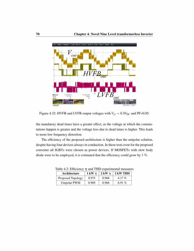
70 Chapter 4. Novel Nine Level transformerless Inverter
Figure 4.32: HVFB and LVFB output voltages with Vf c = 0.5VDC and PF=0.85.
the mandatory dead times have a greater effect, as the voltage at which the commu-
tations happen is greater and the voltage loss due to dead times is higher. This leads
to more low frequency distortion.
The efficiency of the proposed architecture is higher than the unipolar solution,
despite having four devices always in conduction. In these tests even for the proposed
converter all IGBTs were chosen as power devices. If MOSFETs with slow body
diode were to be employed, it is estimated that the efficiency could grow by 1 %.
Table 4.2: Efficiency η and THD experimental measures
Architecture 1 kW η 2 kW η 2 kW THD
Proposed Topology 0.975 0.968 4.17 %
Unipolar PWM 0.969 0.966 6.91 %
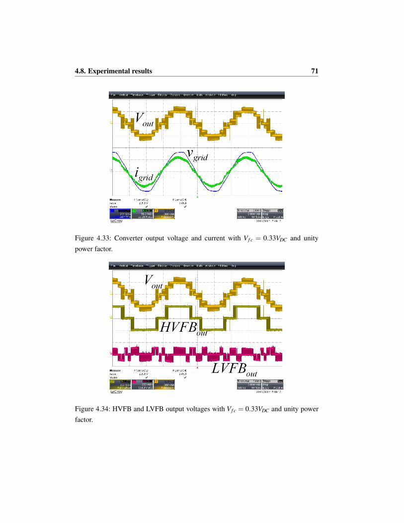
4.8. Experimental results 71
Figure 4.33: Converter output voltage and current with Vf c = 0.33VDC and unity
power factor.
Figure 4.34: HVFB and LVFB output voltages with Vf c = 0.33VDC and unity power
factor.

72 Chapter 4. Novel Nine Level transformerless Inverter
Figure 4.35: Converter output voltage and current with Vf c = 0.66VDC and unity
power factor.
Figure 4.36: HVFB and LVFB output voltages with Vf c = 0.66VDC and unity power
factor.
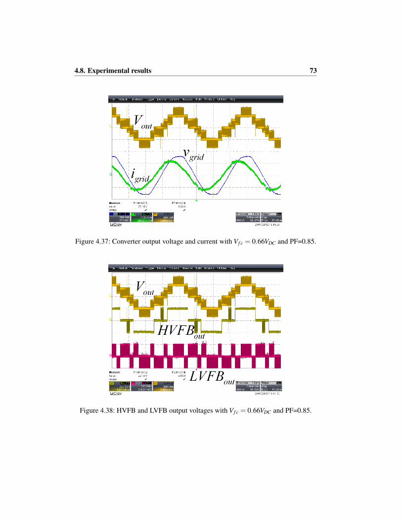
4.8. Experimental results 73
Figure 4.37: Converter output voltage and current with Vf c = 0.66VDC and PF=0.85.
Figure 4.38: HVFB and LVFB output voltages with Vf c = 0.66VDC and PF=0.85.

74 Chapter 4. Novel Nine Level transformerless Inverter
Figure 4.39: Grid current and voltage in case of unipolar PWM and PF=0.1.
Figure 4.40: Common mode voltage at the output of the converter in case of unipolar
PWM.
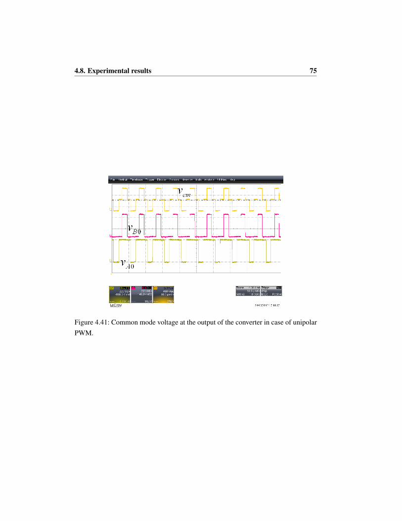
4.8. Experimental results 75
Figure 4.41: Common mode voltage at the output of the converter in case of unipolar
PWM.


Chapter 5
Conclusions
In this thesis several topologies of transformerless grid-connected inverters and mul-
tilevel converters were analyzed, highlighting drawbacks and strengths. A novel con-
verter was proposed and evaluated in terms of grid current quality and ground leakage
current.
The proposed converter relies on the well known cascaded full-bridge topology,
where one of the full-bridges is supplied by a flying capacitor. An appropriate PWM
strategy was developed to reduce the switching losses and the ground leakage current,
that represent a problem of paramount importance in PV-fed grid-connected power
converters.
The key characteristics of the realized inverter are:
• Up to nine level output voltage waveform, that allows to reduce the output
current ripple due to the switching.
• Extended power factor operations.
• Arbitrary DC voltage ratio with unaffected ability to synthesize the desired
output voltage. In fact, even when during a transient the converter enters an
unstable flying capacitor voltage area, the output voltage generation is unaf-
fected.

78 Chapter 5. Conclusions
• Intrinsic boost capabilities, as the charging of the flying capacitor extends the
input voltage sufficient to control the grid current.
• Possibility to employ MOSFETs with slow body diode to reduce the conduc-
tion losses.
• The Transient Circuit allows to keep low levels of ground leakage current.
The proposed solution presents some drawbacks:
• The topology presents an increased component count with respect to the state
of the art.
• During the active phase, there are always four devices conducting, limiting the
maximum obtainable efficiency.
• The continuous power transfer between the HVFB and LVFB can reduce the
lifetime of the flying capacitor.
Simulations and experimental results show that the proposed converter allows to
obtain very good performance regarding grid current distortion and can represent a
feasible solution for PV-fed inverter systems.

Bibliography
[1] Xiao Huafeng and Xie Shaojun. Leakage Current Analytical Model and Appli-
cation in Single-Phase Transformerless Photovoltaic Grid-Connected Inverter.
IEEE Transactions on Electromagnetic Compatibility, 52(4):902 –913, Novem-
ber 2010.
[2] O. Lopez, F. D. Freijedo, A. G. Yepes, P. Fernandez-Comesaa, J. Malvar,
R. Teodorescu, and J. Doval-Gandoy. Eliminating Ground Current in a Trans-
formerless Photovoltaic Application. IEEE Transactions on Energy Conversion,
25(1):140 –147, March 2010.
[3] M. Cacciato, A. Consoli, R. Attanasio, and F. Gennaro. Soft-Switching Con-
verter With HF Transformer for Grid-Connected Photovoltaic Systems. IEEE
Transactions on Industrial Electronics, 57(5):1678 –1686, May 2010.
[4] C. Rodriguez and G.A.J. Amaratunga. Long-Lifetime Power Inverter for Photo-
voltaic AC Modules. IEEE Transactions on Industrial Electronics, 55(7):2593
–2601, July 2008.
[5] M. Ciobotaru, R. Teodorescu, and F. Blaabjerg. Control of single-stage single-
phase PV inverter. In European Conference on Power Electronics and Applica-
tions, September 2005.
[6] P. Rodriguez, A. Luna, I. Candela, R. Mujal, R. Teodorescu, and F. Blaab-
jerg. Multiresonant Frequency-Locked Loop for Grid Synchronization of Power

80 Bibliography
Converters Under Distorted Grid Conditions. IEEE Transactions on Industrial
Electronics, 58(1):127 –138, January 2011.
[7] M. Liserre, F. Blaabjerg, and S. Hansen. Design and control of an LCL-filter-
based three-phase active rectifier. IEEE Transactions on Industry Applications,
41(5):1281 – 1291, September 2005.
[8] A. Timbus, M. Liserre, R. Teodorescu, P. Rodriguez, and F. Blaabjerg. Evalu-
ation of Current Controllers for Distributed Power Generation Systems. IEEE
Transactions on Power Electronics, 24(3):654 –664, March 2009.
[9] T. Hornik and Q. C. Zhong. H infinite repetitive voltage control of grid con-
nected inverters with a frequency adaptive mechanism. IET Power Electronics,
3(6):925–935, November 2010.
[10] M. Odavic, V. Biagini, P. Zanchetta, M. Sumner, and M. Degano. One-
sample-period-ahead predictive current control for high-performance active
shunt power filters. IET Power Electronics, 4(4):414 –423, April 2011.
[11] Shuitao Yang, Qin Lei, F.Z. Peng, and Zhaoming Qian. A Robust Control
Scheme for Grid-Connected Voltage-Source Inverters. IEEE Transactions on
Industrial Electronics, 58(1):202 –212, January 2011.
[12] Mei Qiang, Shan Mingwei, Liu Liying, and J. M. Guerrero. A Novel Im-
proved Variable Step-Size Incremental-Resistance MPPT Method for PV Sys-
tems. IEEE Transactions on Industrial Electronics, 58(6):2427 –2434, June
2011.
[13] R. Kadri, J. P. Gaubert, and G. Champenois. An Improved Maximum Power
Point Tracking for Photovoltaic Grid-Connected Inverter Based on Voltage-
Oriented Control. IEEE Transactions on Industrial Electronics, 58(1):66 –75,
January 2011.
[14] B. Subudhi and R. Pradhan. A Comparative Study on Maximum Power Point
Tracking Techniques for Photovoltaic Power Systems. IEEE Transactions on
Sustainable Energy - In press, available on IEEE Early Access.
Bibliography 81
[15] D. Dong, F. Luo, D. Boroyevich, and P. Mattavelli. Leakage Current Reduction
in a Single-Phase Bidirectional AC/DC Full-Bridge Inverter. IEEE Transactions
on Power Electronics, 27(10):4281 –4291, October 2012.
[16] Wensong Yu, Jih-Sheng Lai, Hao Qian, and C. Hutchens. High-Efficiency
MOSFET Inverter with H6-Type Configuration for Photovoltaic Nonisolated
AC-Module Applications. IEEE Transactions on Power Electronics, 26(4):1253
–1260, April 2011.
[17] B. Gu, J. Dominic, J. Lai, C. Chen, and B. Chen. High Reliability and Effi-
ciency Single-Phase Transformerless Inverter for Grid-Connected Photovoltaic
Systems. IEEE Transactions on Power Electronics, 57(9):3118 –3128, May
2013.
[18] Xiao Huafeng, Xie Shaojun, Chen Yang, and Ruhai Huang. An Optimized
Transformerless Photovoltaic Grid-Connected Inverter. IEEE Transactions on
Industrial Electronics, 58(5):1887 –1895, May 2011.
[19] T. Kerekes, R. Teodorescu, P. Rodriguez, G. Vazquez, and E. Aldabas. A New
High-Efficiency Single-Phase Transformerless PV Inverter Topology. IEEE
Transactions on Industrial Electronics, 58(1):184 –191, January 2011.
[20] R. Gonzalez, J. Lopez, P. Sanchis, and L. Marroyo. Transformerless Inverter for
Single-Phase Photovoltaic Systems. IEEE Transactions on Power Electronics,
22(2):693 –697, March 2007.
[21] G. Buticchi, D. Barater, E. Lorenzani, and G. Franceschini. Digital Control
of Actual Grid-Connected Converters for Ground Leakage Current Reduction
in PV Transformerless Systems. IEEE Transactions on Industrial Informatics,
8(3):563–572, August 2012.
[22] S. V. Araujo, P. Zacharias, and R. Mallwitz. Highly Efficient Single-Phase
Transformerless Inverters for Grid-Connected Photovoltaic Systems. IEEE
Transactions on Industrial Electronics, 28(5):2235–2245, September 2010.

82 Bibliography
[23] Yunjie Gu, Wuhua Li, Yi Zhao, Bo Yang, Chushan Li, and Xiangning He.
Transformerless Inverter With Virtual DC Bus Concept for Cost-Effective Grid-
Connected PV Power Systems. IEEE Transactions on Power Electronics,
28(2):973–805, February 2013.
[24] S. Kouro, M. Malinowski, K. Gopakumar, J. Pou, L. G. Franquelo, Wu Bin,
J. Rodriguez, M. A. Perez, and J. I. Leon. Recent Advances and Industrial
Applications of Multilevel Converters. IEEE Transactions on Industrial Elec-
tronics, 57(8):2553 –2580, August 2010.
[25] S. Daher, J. Schmid, and F. L. M. Antunes. Multilevel Inverter Topologies
for Stand-Alone PV Systems. IEEE Transactions on Industrial Electronics,
55(7):2703–2712, July 2008.
[26] Liao Yi-Hung and Lai Ching-Ming. Newly-Constructed Simplified Single-
Phase Multistring Multilevel Inverter Topology for Distributed Energy Re-
sources. IEEE Transactions on Power Electronics, 26(9):2386–2392, Septem-
ber 2011.
[27] E. Villanueva, P. Correa, J. Rodriguez, and M. Pacas. Control of a Single-Phase
Cascaded H-Bridge Multilevel Inverter for Grid-Connected Photovoltaic Sys-
tems. IEEE Transactions on Industrial Electronics, 56(11):4399–4406, Novem-
ber 2009.
[28] Jih-Sheng Lai and Fang Zheng Peng. Multilevel converters-a new breed of
power converters. IEEE Transactions on Industry Applications, 32(3):509 –
517, May 1996.
[29] J. Pou, R. Pindado, and D. Boroyevich. Voltage-balance limits in four-level
diode-clamped converters with passive front ends. IEEE Transactions Industrial
Electronics, 52(1):190 – 196, February 2005.
[30] A. Shukla, A. Ghosh, and A. Joshi. Control Schemes for DC Capacitor Voltages
Equalization in Diode-Clamped Multilevel Inverter-Based DSTATCOM. IEEE
Transactions on Power Delivery, 23(2):1139 –1149, April 2008.
Bibliography 83
[31] N. Celanovic and D. Boroyevich. A comprehensive study of neutral-point
voltage balancing problem in three-level neutral-point-clamped voltage source
PWM inverters. IEEE Transactions on Power Electronics, 15(2):242 –249,
March 2000.
[32] A. Bendre, G. Venkataramanan, D. Rosene, and V. Srinivasan. Modeling and
design of a neutral-point voltage regulator for a three-level diode-clamped in-
verter using multiple-carrier modulation. IEEE Transactions Industrial Elec-
tronics, 53(3):718 – 726, June 2006.
[33] L. Zhang and S.J. Watkins. Capacitor voltage balancing in multilevel flying ca-
pacitor inverters by rule-based switching pattern selection. IET Electric Power
Applications, 1(3):339 –347, May 2007.
[34] R. Gonzalez, E. Gubia, J. Lopez, and L. Marroyo. Transformerless Single-
Phase Multilevel-Based Photovoltaic Inverter. IEEE Transactions on Industrial
Electronics, 55(7):2694 –2702, July 2008.
[35] C. Cecati, F. Ciancetta, and P. Siano. A Multilevel Inverter for Photovoltaic
Systems With Fuzzy Logic Control. IEEE Transactions Industrial Electronics,
57(12):4115 –4125, December 2010.
[36] Sung Geun Song, Feel Soon Kang, and Sung-Jun Park. Cascaded Multilevel In-
verter Employing Three-Phase Transformers and Single DC Input. IEEE Trans-
actions Industrial Electronics, 56(6):2005 –2014, June 2009.
[37] M. Malinowski, K. Gopakumar, J. Rodriguez, and M.A. Perez. A Survey
on Cascaded Multilevel Inverters. IEEE Transactions Industrial Electronics,
57(7):2197 –2206, July 2010.
[38] Yiqiao Liang and C.O. Nwankpa. A new type of STATCOM based on cascad-
ing voltage-source inverters with phase-shifted unipolar SPWM. IEEE Trans-
actions on Industry Applications, 35(5):1118 –1123, September 1999.
84 Bibliography
[39] J.I. Leon, R. Portillo, S. Vazquez, J.J. Padilla, L.G. Franquelo, and J.M. Car-
rasco. Simple Unified Approach to Develop a Time-Domain Modulation Strat-
egy for Single-Phase Multilevel Converters. IEEE Transactions Industrial Elec-
tronics, 55(9):3239 –3248, September 2008.
[40] J.I. Leon, S. Vazquez, A.J. Watson, L.G. Franquelo, P.W. Wheeler, and J.M.
Carrasco. Feed-Forward Space Vector Modulation for Single-Phase Multilevel
Cascaded Converters With Any DC Voltage Ratio. IEEE Transactions Indus-
trial Electronics, 56(2):315 –325, February 2009.
[41] Yun Zhang and Li Sun. An Efficient Control Strategy for a Five-Level Inverter
Comprising Flying-Capacitor Asymmetric H-Bridge. IEEE Transactions In-
dustrial Electronics, 58(9):4000 –4009, September 2011.
[42] D.A. Ruiz-Caballero, R.M. Ramos-Astudillo, S.A. Mussa, and M.L. Heldwein.
Symmetrical Hybrid Multilevel DC-AC Converters With Reduced Number of
Insulated DC Supplies. IEEE Transactions Industrial Electronics, 57(7):2307
–2314, July 2010.
[43] Sung-Jun Park, Feel-Soon Kang, Man Hyung Lee, and Cheul-U Kim. A new
single-phase five-level PWM inverter employing a deadbeat control scheme.
IEEE Transactions on Power Electronics, 18(3):831 – 843, May 2003.
[44] J. Selvaraj and N.A. Rahim. Multilevel Inverter For Grid-Connected PV System
Employing Digital PI Controller. IEEE Transactions Industrial Electronics,
56(1):149 –158, January 2009.
[45] N.A. Rahim and J. Selvaraj. Multistring Five-Level Inverter With Novel PWM
Control Scheme for PV Application. IEEE Transactions Industrial Electronics,
57(6):2111 –2123, June 2010.
[46] N.A. Rahim, K. Chaniago, and J. Selvaraj. Single-Phase Seven-Level Grid-
Connected Inverter for Photovoltaic System. IEEE Transactions Industrial
Electronics, 58(6):2435 –2443, June 2011.

Bibliography 85
[47] S. S. Fazel, S Bernet, D. Krug, and K. Jalili. Design and Comparison of 4-
kV Neutral-Point-Clamped, Flying-Capacitor, and Series-Connected H-Bridge
Multilevel Converters. IEEE Transactions on Industry Applications, 43(4):1032
–1040, July 2007.
[48] A. Varschavsky, J. Dixon, M. Rotella, and L. Moran. Cascaded Nine-Level In-
verter for Hybrid-Series Active Power Filter, Using Industrial Controller. IEEE
Transactions on Industrial Electronics, 57(8):2761 –2767, August 2010.
[49] V.M.E. Antunes, V.F. Pires, and J.F.A. Silva. Narrow Pulse Elimination PWM
for Multilevel Digital Audio Power Amplifiers Using Two Cascaded H-Bridges
as a Nine-Level Converter. IEEE Transactions on Power Electronics, 22(2):425
–434, March 2007.
[50] D. A. B. Zambra, C. Rech, and J. R. Pinheiro. Comparison of Neutral-Point-
Clamped, Symmetrical, and Hybrid Asymmetrical Multilevel Inverters. IEEE
Transactions on Industrial Electronics, 57(7):2297 –2306, July 2010.
[51] S. P. Pimentel and J. A. Pomilio. Asynchronous distributed generation system
based on asymmetrical cascaded multilevel inverter. In IEEE IECON’08, pages
3227 –3232, November 2008.
[52] Ebrahim Babaei and Seyed Hossein Hosseini. New cascaded multilevel inverter
topology with minimum number of switches. Energy Conversion and Manage-
ment, 50(11):2761 – 2767, November 2009.
[53] L. A. Silva, S. P. Pimentel, and J. A. Pomilio. Nineteen-level Active Filter
System using Asymmetrical Cascaded Converter with DC Voltages Control. In
IEEE 36th Power Electronics Specialists Conference, PESC ’05., pages 303 –
308, June 2005.


1
1
2
2
3
3
4
4
H H
G G
F F
E E
D D
C C
B B
A A
EMU0100
TRSTn99
TDO98
TDI97
5V96
GPIO-3395
GPIO-3194
GPIO-29/SCITXDA93
5V92
GPIO-23/EQEP1I91
GPIO-21/EQEP1B90
GPIO-19/SPISTEA89
GPIO-17/SPISOMIA88
5V87
GPIO-2786
GPIO-2585
GPIO-1484
GPIO-1383
5V82
GPIO-8581
GPIO-4980
GPIO-1179
GPIO-0978
5V77
GPIO-07/EPWM4B76
GPIO-05/EPWM3B75
GPIO-03/EPWM2B74
GPIO-01/EPWM1B73
GPIO-6372
ADC-A771
GPIO-6170
ADC-A669
GPIO-5968
ADC-A567
NC66
ADC-A465
AGND64
ADC-A363
AGND62
ADC-A261
AGND60
ADC-A159
AGND58
ADC-A057
GND-ISO56
NC55
NC54
NC53
ISO-TX52
V33-ISO51
V33-ISO1ISO-RX2
NC 3NC 4NC 5
GND-ISO 6
ADC-B0 7AGND 8
ADC-B1 9AGND 10
ADC-B211AGND12ADC-B313AGND14ADC-B415NC16ADC-B517GPIO-5818ADC-B619GPIO-6020
ADC-B7 21GPIO_62 22
GPIO-00/EPWM1A 23GPIO-02/EPWM2A 24GPIO-04/EPWM3A 25GPIO-06/EPWM4A 26
DGND 27GPIO-08 28GPIO-10
29GPIO-4830GPIO-8431GPIO-8632GPIO-1233GPIO-1534GPIO-2435GPIO-2636DGND37GPIO-16/SPISIMOA38
GPIO-18/SPICLKA 39GPIO-20/EQEP1A 40GPIO-22/EQEP1S 41
GPIO-87 42GPIO-28/SCIRXDA 43
GPIO-30 44GPIO-32 45GPIO-34 46
DGND 47TCK 48TMS
49EMU150
DIM100
DIM100
Vin1
Vout3
GN
D2
U3
ld29150xx33
D1BAV99
Vdd5
MRn3
WDI4
Gnd2
RSTn 1
U1
TPS3828
Out2 IN 3
GN
D1
Out4
U2NX1117C
DGND
AGND
3.3V
1.9V
22uHL1L2L3L4L5L6
L7L8L9L10
L11L12L13L14L15L16
L17L18
100nF
100nF
DGND
DGND
Reset
Reset
AGND
5V
5V
5V 3.3V
DGND
DGND
1.9V
100nFC1
DGND
1uFC5
DGND
1uFC3
100uC4
2K
R1
3.3V
3.3V
GPIO-58GPIO-59GPIO-60GPIO-61GPIO-62GPIO-63GPIO-84
GPIO-85GPIO-86GPIO-87
3K3
R30
3.3V
3K3
R29
3K3
R28
3K3
R27
GPIO-87
GPIO-86GPIO-84GPIO-85
GPIO-48GPIO-49
GPIO-49 GPIO-48
100nFC2
DGND
TCKTMSTDITDOEMU0EMU1
EMU0TRSTnTDOTDI
TCKTMSEMU1
TRSTn
XCLK-IN
XCLK-IN
DGND
0R
R16
GPIO-30GPIO-31
GPIO-32GPIO-33GPIO-34
GPIO-16GPIO-17GPIO-18GPIO-19GPIO-20GPIO-21GPIO-22GPIO-23GPIO-24GPIO-25GPIO-26GPIO-27
ADC-A0
ADC-A1
ADC-A2
ADC-A3
ADC-A4
ADC-A5
ADC-A6
ADC-A7
ADC-B0
ADC-B1
ADC-B2
ADC-B3
ADC-B4
ADC-B5
ADC-B6
ADC-B7
33R GPIO-00GPIO-01GPIO-02GPIO-03GPIO-04GPIO-05GPIO-06GPIO-07
VdPL3384
VDIO339
VDIO3371
VDIO3393
VDIO33107
VDIO33121
VDIO33143
VDIO33159
VDIO33170
VdADC3334
VdADC3345
Vdd184
Vdd1815
Vdd1823
Vdd1829
Vdd1861
Vdd18101
Vdd18109
Vdd18117
Vdd18126
Vdd18139
Vdd18146
Vdd18154
VdADC1831
VdADC1859
XRSn80
XCLK-IN105
XCLK-OUT138
TEST181
TRSTn78
TEST282
TCK87
TMS79
TD176
TD077
EMU085
EMU186
X1104
X2102
Dgnd3
Dgnd8
Dgnd14
Dgnd22
Dgnd30
Dgnd60
Dgnd70
Dgnd83
Dgnd92
Dgnd103
Dgnd106
Dgnd108
Dgnd118
Dgnd120
Dgnd125
Dgnd140
Dgnd144
Dgnd147
Dgnd155
Dgnd160
Dgnd166
Dgnd171
ADCGnd33
ADCGnd44
ADCGnd32
ADCGnd58
ADC-A0 42
ADC-A1 41
ADC-A2 40
ADC-A339
ADC-A438
ADC-A537
ADC-A636
ADC-A735
ADC-B046
ADC-B147
ADC-B248
ADC-B349
ADC-B4 50
ADC-B5 51
ADC-B6 52
ADC-B7 53
ADC-REFIN54
ADC_LO 43ADC-RESETXT 57
ADC-REFM 55ADC-REFP 56
GPIO-005
GPIO-016
GPIO-027
GPIO-0310
GPIO-0411
GPIO-0512
GPIO-0613
GPIO-07 16
GPIO-08 17
GPIO-09 18
GPIO-10 19
GPIO-11 20
GPIO-12 21
GPIO-13 24
GPIO-14 25
GPIO-15 26
GPIO-1627
GPIO-1728
GPIO-1862
GPIO-1963
GPIO-2064
GPIO-2165
GPIO-2266
GPIO-2367
GPIO-2468
GPIO-2569
GPIO-26 72
GPIO-27 73
GPIO-28 141
GPIO-29 2
GPIO-30 1
GPIO-31 176
GPIO-32 74
GPIO-33 75
GPIO-34142
GPIO-35148
GPIO-36145
GPIO-37150
GPIO-38137
GPIO-39175
GPIO-40151
GPIO-41152
GPIO-42153
GPIO-43156
GPIO-44157
GPIO-45 158
GPIO-46 161
GPIO-47 162
GPIO-48 88
GPIO-49 89
GPIO-50 90
GPIO-51 91
GPIO-52 94
GPIO-5395
GPIO-5496
GPIO-5597
GPIO-5698
GPIO-5799
GPIO-58100
GPIO-59110
GPIO-60111
GPIO-61112
GPIO-62113
GPIO-63114
GPIO-64 115
GPIO-65 116
GPIO-66 119
GPIO-82165 GPIO-81164 GPIO-88163 GPIO-79136 GPIO-78135 GPIO-77134 GPIO-76133 GPIO-75132 GPIO-74131
GPIO-73130GPIO-72129GPIO-71128GPIO-78127GPIO-69124GPIO-68123GPIO-67122
GPIO-83168
GPIO-84169
GPIO-85172
GPIO-86173
GPIO-87174
XRDn149
U4
TMS320F28335
GPIO-08GPIO-09GPIO-10GPIO-11GPIO-12GPIO-13GPIO-14GPIO-15
GPIO-26GPIO-24GPIO-15GPIO-12
GPIO-10GPIO-08
GPIO-06GPIO-04GPIO-02GPIO-00GPIO-01
GPIO-03GPIO-05GPIO-07
GPIO-09GPIO-11
GPIO-13GPIO-14GPIO-25GPIO-27
GPIO-23GPIO-21GPIO-19GPIO-17
GPIO-33GPIO-31
GPIO-34GPIO-32GPIO-30
GPIO-22GPIO-20GPIO-18GPIO-16
GPIO-62
GPIO-60
GPIO-58
GPIO-63
GPIO-61
GPIO-59
X1X2
22K1
R4 AGND
2u2C20
2u2C21
AGND
DGND
AGND
3.3V
56RR2
3n3C19
ADC-A0
D2BAV99
AGND
3.3V
56RR3
3n3C22
ADC-A1
D3BAV99
AGND
3.3V
56RR5
3n3C23
ADC-A2
D4BAV99
AGND
3.3V
56RR11
3n3C29
ADC-A3
D5BAV99
AGND
3.3V
56RR15
3n3C30
ADC-A4
D6BAV99
AGND
3.3V
56RR17
3n3C31
ADC-A5
D7BAV99
AGND
3.3V
56RR18
3n3C32
ADC-A6
D8BAV99
AGND
3.3V
56RR19
3n3C33
ADC-A7
D9BAV99
AGND
3.3V
56RR20
3n3C34
ADC-B0
D11BAV99
AGND
3.3V
56RR22
3n3C36
ADC-B1
D13BAV99
AGND
3.3V
56RR24
3n3C38
ADC-B2
D14BAV99
AGND
3.3V
56RR26
3n3C39
ADC-B4D15BAV99
AGND
3.3V
56R
R25
3n3C40
ADC-B3
D12BAV99
AGND
3.3V
56RR23
3n3C37
ADC-B5
AGND
3.3V
56RR21
3n3C35
ADC-B6
AGND
3.3V
56RR31
3n3C41
ADC-B7
D10BAV99
D16BAV99
18pFC42
DGND
18pFC43
DGND
0R
R32_NM
DGND
X1 X21 2Y1
ABM7-30.000MHz-D2Y
10uFC44
10uFC45
3.3V
4K7
R33
4K7
R34
EMU0EMU1
TRSTn
2K2
R32
DGND
DGND AGND
0R
R35
3.3V
DGND
1K6
R37
D18LED2
DGND
820R
R36
D17LED2
1.9V
AGND
Reset
0R
R38_NM
3.3V
Fusion
Font monospazio
Control Card Schematic A1.1
Fusion
Nota
Accepted impostata da Fusion

PAC102PAC101
COC1
PAC202PAC201 COC2
PAC302
PAC301
COC3
PAC401PAC402
COC4
PAC502PAC501
COC5
PAC602PAC601COC6
PAC702PAC701
COC7
PAC802PAC801COC8 PAC902PAC901COC9 PAC1002PAC1001COC10
PAC1102PAC1101
COC11
PAC1202PAC1201
COC12
PAC1302PAC1301
COC13
PAC1402PAC1401
COC14
PAC1502PAC1501
COC15
PAC1602PAC1601
COC16
PAC1702PAC1701
COC17
PAC1802PAC1801
COC18
PAC1902PAC1901
COC19
PAC2002
PAC2001COC20
PAC2102
PAC2101COC21
PAC2202PAC2201COC22
PAC2302PAC2301COC23
PAC2402PAC2401COC24
PAC2502PAC2501
COC25PAC2602PAC2601
COC26
PAC2702PAC2701COC27
PAC2802PAC2801COC28
PAC2902PAC2901COC29
PAC3002PAC3001COC30
PAC3102PAC3101COC31
PAC3202PAC3201COC32
PAC3302PAC3301COC33
PAC3402PAC3401COC34
PAC3502PAC3501COC35
PAC3602PAC3601COC36
PAC3702PAC3701COC37
PAC3802PAC3801COC38
PAC3902PAC3901COC39
PAC4002PAC4001
COC40PAC4102PAC4101
COC41
PAC4202PAC4201
COC42
PAC4302PAC4301
COC43
PAC4402PAC4401
COC44
PAC4502
PAC4501COC45
PAD103
PAD102PAD101
COD1PAD203
PAD202PAD201
COD2
PAD303
PAD302PAD301
COD3
PAD403
PAD402PAD401
COD4
PAD503
PAD502PAD501
COD5PAD603
PAD602PAD601
COD6
PAD703
PAD702PAD701
COD7
PAD803
PAD802PAD801
COD8
PAD903
PAD902PAD901COD9
PAD1003
PAD1002PAD1001COD10
PAD1103
PAD1102PAD1101COD11
PAD1203
PAD1202PAD1201
COD12
PAD1303
PAD1302PAD1301COD13
PAD1403
PAD1402PAD1401COD14
PAD1503
PAD1502PAD1501
COD15
PAD1603
PAD1602PAD1601
COD16
PAD1701
PAD1702COD17
PAD1801
PAD1802COD18
PADIM10001PADIM10004
PADIM10003PADIM10002
PADIM10006PADIM10005
PADIM100011PADIM100012PADIM10008PADIM10009PADIM100010
PADIM10007PADIM100013
PADIM100016PADIM100015
PADIM100014PADIM100018
PADIM100017PADIM100021PADIM100022
PADIM100019PADIM100020PADIM100036
PADIM100035PADIM100038
PADIM100037PADIM100033PADIM100034
PADIM100030PADIM100031PADIM100032PADIM100029
PADIM100023PADIM100026
PADIM100025PADIM100024
PADIM100028PADIM100027
PADIM100049PADIM100050PADIM100046PADIM100047PADIM100048
PADIM100045PADIM100039
PADIM100042PADIM100041
PADIM100040PADIM100044
PADIM100043PADIM100093PADIM100094PADIM100090PADIM100091PADIM100092
PADIM100089PADIM100095
PADIM100098PADIM100097
PADIM100096PADIM1000100
PADIM100099PADIM100077PADIM100078
PADIM100074PADIM100075PADIM100076PADIM100073
PADIM100079PADIM100082
PADIM100081PADIM100080
PADIM100084PADIM100083
PADIM100087PADIM100088PADIM100085PADIM100086
PADIM100070PADIM100069
PADIM100072PADIM100071
PADIM100067PADIM100068PADIM100064PADIM100065PADIM100066
PADIM100063PADIM100057
PADIM100060PADIM100059
PADIM100058PADIM100062
PADIM100061PADIM100055PADIM100056
PADIM100052PADIM100053PADIM100054PADIM100051
CODIM100
PAL102PAL101
COL1
PAL202
PAL201COL2
PAL302PAL301
COL3
PAL402PAL401 COL4
PAL502PAL501 COL5
PAL602
PAL601 COL6PAL702
PAL701COL7
PAL802
PAL801COL8
PAL902
PAL901 COL9PAL1002
PAL1001COL10
PAL1102
PAL1101COL11
PAL1202
PAL1201COL12
PAL1302
PAL1301COL13
PAL1402
PAL1401COL14
PAL1502
PAL1501COL15PAL1602
PAL1601COL16
PAL1702
PAL1701COL17
PAL1802
PAL1801COL18
PAR102PAR101
COR1
PAR202PAR201COR2PAR302PAR301COR3
PAR402PAR401COR4
PAR502PAR501
COR5
PAR602PAR601
COR6
PAR702PAR701
COR7PAR802
PAR801COR8
PAR902PAR901
COR9PAR1002
PAR1001COR10
PAR1102PAR1101
COR11
PAR1202PAR1201
COR12PAR1302
PAR1301COR13
PAR1402PAR1401COR14
PAR1502PAR1501
COR15
PAR1602PAR1601
COR16
PAR1702PAR1701
COR17PAR1802PAR1801
COR18PAR1902PAR1901
COR19
PAR2002PAR2001COR20
PAR2102PAR2101
COR21
PAR2202PAR2201
COR22PAR2302PAR2301
COR23
PAR2402PAR2401
COR24
PAR2502PAR2501COR25
PAR2602PAR2601COR26
PAR2702PAR2701
COR27
PAR2802PAR2801
COR28
PAR2902PAR2901
COR29
PAR3002PAR3001
COR30
PAR3102PAR3101COR31
PAR3202PAR3201COR32 PAR320NM02
PAR320NM01
COR320NM
PAR3302PAR3301 COR33
PAR3402PAR3401COR34
PAR3502PAR3501
COR35
PAR3602PAR3601
COR36
PAR3702PAR3701
COR37
PAR380NM02PAR380NM01
COR380NM
PAU105
PAU104PAU103PAU102PAU101
COU1
PAU204 PAU203PAU202
PAU201COU2
PAU303 PAU302PAU301
COU3
PAU401
PAU402
PAU403
PAU404
PAU405
PAU406
PAU407
PAU408
PAU409PAU4010PAU4011PAU4012PAU4013PAU4014PAU4015PAU4016PAU4017PAU4018PAU4019PAU4020PAU4021PAU4022PAU4023PAU4024PAU4025PAU4026PAU4027PAU4028PAU4029PAU4030PAU4031PAU4032PAU4033PAU4034PAU4035PAU4036PAU4037PAU4038PAU4039PAU4040PAU4041PAU4042PAU4043PAU4044PAU4045PAU4046PAU4047PAU4048PAU4049PAU4050PAU4051PAU4052PAU4053PAU4054PAU4055PAU4056PAU4057PAU4058PAU4059PAU4060PAU4061PAU4062PAU4063PAU4064PAU4065PAU4066PAU4067PAU4068PAU4069PAU4070PAU4071PAU4072PAU4073PAU4074PAU4075PAU4076PAU4077PAU4078PAU4079PAU4080PAU4081PAU4082PAU4083PAU4084PAU4085PAU4086PAU4087PAU4088
PAU4089PAU4090PAU4091PAU4092PAU4093PAU4094PAU4095PAU4096PAU4097PAU4098PAU4099PAU40100PAU40101PAU40102PAU40103PAU40104PAU40105PAU40106PAU40107PAU40108PAU40109PAU40110PAU40111PAU40112PAU40113PAU40114PAU40115PAU40116PAU40117PAU40118PAU40119PAU40120PAU40121PAU40122PAU40123PAU40124PAU40125PAU40126PAU40127PAU40128PAU40129PAU40130PAU40131PAU40132
PAU40133PAU40134PAU40135
PAU40136PAU40137
PAU40138PAU40139PAU40140PAU40141
PAU40142PAU40143
PAU40144PAU40145PAU40146
PAU40147PAU40148PAU40149PAU40150
PAU40151PAU40152PAU40153
PAU40154PAU40155PAU40156
PAU40157PAU40158PAU40159PAU40160
PAU40161PAU40162
PAU40163PAU40164PAU40165
PAU40166PAU40167PAU40168PAU40169
PAU40170PAU40171PAU40172
PAU40173PAU40174PAU40175
PAU40176COU4
PAY102
PAY101COY1
Fusion
Font monospazio
Control Card PCB A1.2
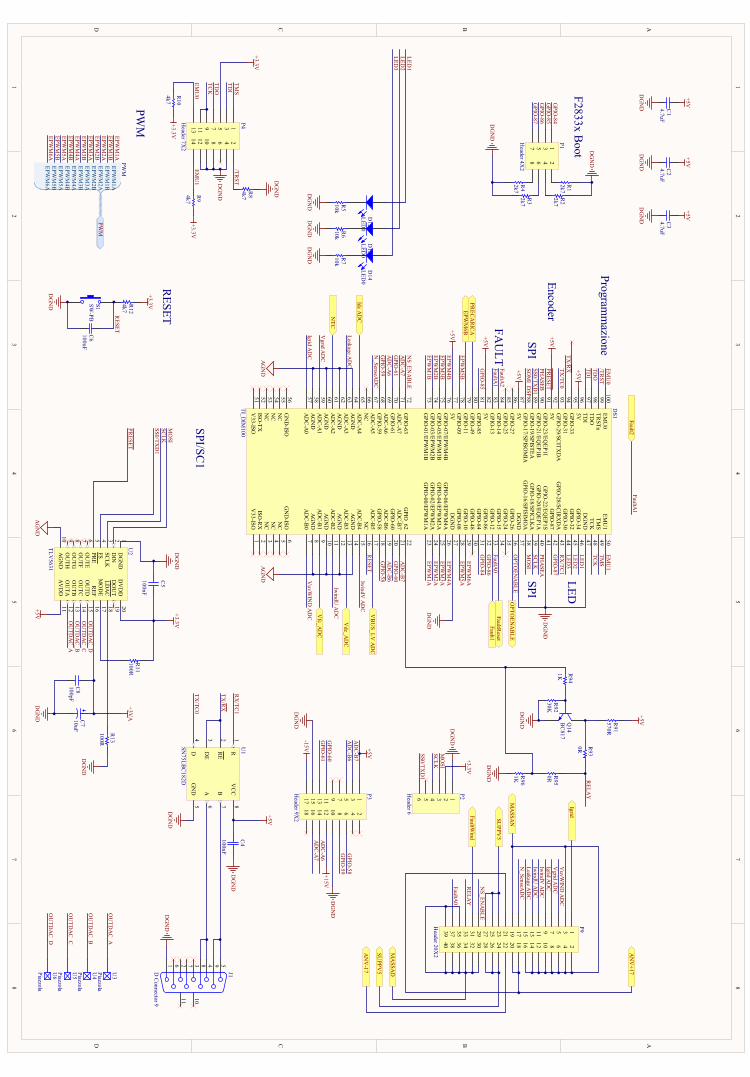
1 1
2 2
3 3
4 4
5 5
6 6
7 7
8 8
DD
CC
BB
AA
TCK
TMS
TDI
TDO
/TRST
MO
SISC
LKSS0/TX
D1
+3.3VS1SW-PB
DG
ND
MO
SISC
LK
RX
/TC1
TX/TC
0
SPI/SC1
Programm
azione
PWM
RESETRESET
Encoder
FAU
LTFaultA
0FaultA
1FaultA
2
LED3
SPI
EPWM
1AEPW
M1B
EPWM
2AEPW
M2B
EPWM
3AEPW
M3B
EPWM
4AEPW
M4B
EPWM
5AEPW
M5B
EPWM
6A
PWM
PWM
SS0/TXD
1
PHA
SEAPH
ASEB
LED2
LED1
LED3
LED2
LED1
LED
DG
ND
DG
ND
DG
ND
D12
LED0
D13
LED0
D14
LED0
SPI
EPWM
1AEPW
M1B
EPWM
2AEPW
M2B
EPWM
3AEPW
M3B
DG
ND
DG
ND
/TRST
TDO
TMS
TCK
EMU
0EM
U1
EMU
1EM
U0
DG
ND
TDI
+3.3V
+5V
+5V
+5V
+5V
GPIO
-84G
PIO-85
GPIO
-86
GPIO
-87G
PIO-84
GPIO
-85G
PIO-86
GPIO
-87
DG
ND
DG
ND
F2833x Boot
EPWM
4AEPW
M4B
EPWM
6A
12
34
56
78
910
1112
1314
P4Header 7X
2 12
34
56
78
P1Header 4X
2
EPWM
5AEPW
M5B
DG
ND
+5V
DG
ND
+5V
DG
ND
+5V
+3.3V
+3.3V
DG
ND
RESET
EMU
0100
TRSTn
99
TDO
98
TDI
97
5V96
GPIO
-3395
GPIO
-3194
GPIO
-29/SCITX
DA
93
5V92
GPIO
-23/EQEP1I
91
GPIO
-21/EQEP1B
90
GPIO
-19/SPISTEA89
GPIO
-17/SPISOM
IA88
5V87
GPIO
-2786
GPIO
-2585
GPIO
-1484
GPIO
-1383
5V82
GPIO
-8581
GPIO
-4980
GPIO
-1179
GPIO
-0978
5V77
GPIO
-07/EPWM
4B76
GPIO
-05/EPWM
3B75
GPIO
-03/EPWM
2B74
GPIO
-01/EPWM
1B73
GPIO
-6372
AD
C-A
771
GPIO
-6170
AD
C-A
669
GPIO
-5968
AD
C-A
567
NC
66
AD
C-A
465
AG
ND
64
AD
C-A
363
AG
ND
62
AD
C-A
261
AG
ND
60
AD
C-A
159
AG
ND
58
AD
C-A
057
GN
D-ISO
56
NC
55
NC
54
NC
53
ISO-TX
52
V33-ISO
51V
33-ISO1
ISO-R
X2
NC
3N
C4
NC
5G
ND
-ISO6
AD
C-B
07
AG
ND
8A
DC
-B1
9A
GN
D10
AD
C-B
211
AG
ND
12A
DC
-B3
13A
GN
D14
AD
C-B
415
NC
16A
DC
-B5
17G
PIO-58
18A
DC
-B6
19G
PIO-60
20A
DC
-B7
21G
PIO_62
22
GPIO
-00/EPWM
1A23
GPIO
-02/EPWM
2A24
GPIO
-04/EPWM
3A25
GPIO
-06/EPWM
4A26
DG
ND
27G
PIO-08
28G
PIO-10
29G
PIO-48
30G
PIO-84
31G
PIO-86
32G
PIO-12
33G
PIO-15
34G
PIO-24
35G
PIO-26
36D
GN
D37
GPIO
-16/SPISIMO
A38
GPIO
-18/SPICLK
A39
GPIO
-20/EQEP1A
40G
PIO-22/EQ
EP1S41
GPIO
-8742
GPIO
-28/SCIR
XD
A43
GPIO
-3044
GPIO
-3245
GPIO
-3446
DG
ND
47TC
K48
TMS
49EM
U1
50D
S1
TI_DIM
100
EPWM
1AEPW
M1B
EPWM
2AEPW
M2B
EPWM
3AEPW
M3B
EPWM
4AEPW
M4B
EPWM
5AEPW
M5B
EPWM
6A
SOM
I_DSP
AG
ND
AG
ND
Fault1
Vfc_A
DC
Vdc_A
DC
4.7uFC
1
2k7R
1
10kR
5
4.7uFC
24.7uFC
3
10kR
610kR
7
2k7R
2
2k7R
3
2k7R
4
4k7
R9
4k7
R10
4k7R
8
4k7R
12
100nFC
6
12
34
56
78
910
1112
1314
1516
1718
P3Header 9X
2
DG
ND
+3.3V
AG
ND
PRESET
+5V
+3VA
DG
ND
R1
RE
2
DE
3
D4
VC
C8
B7
A6
GN
D5
U1
SN75LB
C182D
DG
ND
1
DIN
2
SCLK
3
FS4
PRE
5
OU
TE6
OU
TF7
OU
TG8
OU
TH9
AG
ND
10
DV
DD
20
DO
UT
19
LDA
C18
MO
DE
17
REF
16
OU
TD15
OU
TC14
OU
TB13
OU
TA12
AV
DD
11
U2
TLV5631
+5V
DG
ND
1 2 3 4 56 7 8 9
11 10
J1D C
onnector 9
GPIO
-58G
PIO-59
GPIO
-60G
PIO-61
AD
C-A
6A
DC
-A7
+15V
-15V +5V
DG
ND
DG
ND
TX/TC
0
RX
/TC1
TX/R
X
TX/R
X
Leakage AD
C
Vgrid A
DC
Igrid AD
C
IwindU
AD
C
VuvW
IND
AD
C
IwindV
AD
C
DG
ND
100R
R13
DG
ND
100nF
C5
100pFC
8
100nF
C4
DG
ND
GPIO
-61
GPIO
-59G
PIO-58
GPIO
-60
123456
P2Header 6
MO
SISC
LK
SS0/TXD
1
DG
ND
+3.3V
Fault2FaultA
1
FaultReset
PREC
AR
ICA
100RR
11
10uFC
7
+5V
OU
TDA
C_D
OU
TDA
C_C
OU
TDA
C_B
OU
TDA
C_A
OU
TDA
C_A
OU
TDA
C_B
OU
TDA
C_C
OU
TDA
C_D
U3
PiazzolaU
4
PiazzolaU
5
PiazzolaU
6
Piazzola
PRESET
AD
C-B
7A
DC
-B6
AD
C-A
7
AD
C-A
6
AD
C-B
7
AD
C-B
6
EPWM
6B
DG
ND
Idc AD
CNTC
RELA
Y
NS_EN
AB
LE
FaultA0
N_SenseA
DC
AN
V-17
Q14
BC
817
570RR
91
1K R94
0R R95
1K R96
0R R93
30KR
92
+5V
DG
ND
N_SenseA
DC
SUPPV
5
AN
V+17
MA
SSAD
MA
SSAN
12
34
56
78
910
1112
1314
1516
1718
1920
2122
2324
2526
2728
2930
3132
3334
3536
3738
3940
P9Header 20X
2
Vgrid A
DC
Leakage AD
C
VuvW
IND
AD
C
IwindU
AD
C
SUPPV
5
NS_EN
AB
LE
RELA
YFaultW
ind
Igrid
IwindV
AD
CIgrid A
DC
VB
US_LV
AD
C
OPTO
ENA
BLE
OPTO
ENA
BLE
PIC101 PIC102COC1
PIC201 PIC202COC2
PIC301 PIC302COC3
PIC401PIC402
COC4
PIC501PIC502 COC5
PIC601 PIC602COC6
PIC701PIC702 COC7
PIC801 PIC802COC8
PID1201PID1202COD12 PID1301PID1302
COD13 PID1401PID1402COD14
PIDS101
PIDS102
PIDS103
PIDS104
PIDS105
PIDS106
PIDS107
PIDS108
PIDS109
PIDS1010
PIDS1011
PIDS1012
PIDS1013
PIDS1014
PIDS1015
PIDS1016
PIDS1017
PIDS1018
PIDS1019
PIDS1020
PIDS1021
PIDS1022
PIDS1023
PIDS1024
PIDS1025
PIDS1026
PIDS1027
PIDS1028
PIDS1029
PIDS1030
PIDS1031
PIDS1032
PIDS1033
PIDS1034
PIDS1035
PIDS1036
PIDS1037
PIDS1038
PIDS1039
PIDS1040
PIDS1041
PIDS1042
PIDS1043
PIDS1044
PIDS1045
PIDS1046
PIDS1047
PIDS1048
PIDS1049
PIDS1050
PIDS1051
PIDS1052
PIDS1053
PIDS1054
PIDS1055
PIDS1056
PIDS1057
PIDS1058
PIDS1059
PIDS1060
PIDS1061
PIDS1062
PIDS1063
PIDS1064
PIDS1065
PIDS1066
PIDS1067
PIDS1068
PIDS1069
PIDS1070
PIDS1071
PIDS1072
PIDS1073
PIDS1074
PIDS1075
PIDS1076
PIDS1077
PIDS1078
PIDS1079
PIDS1080
PIDS1081
PIDS1082
PIDS1083
PIDS1084
PIDS1085
PIDS1086
PIDS1087
PIDS1088
PIDS1089
PIDS1090
PIDS1091
PIDS1092
PIDS1093
PIDS1094
PIDS1095
PIDS1096
PIDS1097
PIDS1098
PIDS1099
PIDS10100 CODS1
PIJ101
PIJ102
PIJ103
PIJ104
PIJ105
PIJ106
PIJ107
PIJ108
PIJ109
PIJ1010
PIJ1011
COJ1
PIP101
PIP102
PIP103
PIP104
PIP105
PIP106
PIP107
PIP108
COP1
PIP201
PIP202
PIP203
PIP204
PIP205
PIP206 COP2
PIP301
PIP302
PIP303
PIP304
PIP305
PIP306
PIP307
PIP308
PIP309
PIP3010
PIP3011
PIP3012
PIP3013
PIP3014
PIP3015
PIP3016
PIP3017
PIP3018
COP3
PIP401
PIP402
PIP403
PIP404
PIP405
PIP406
PIP407
PIP408
PIP409
PIP4010
PIP4011
PIP4012
PIP4013
PIP4014
COP4
PIP901
PIP902
PIP903
PIP904
PIP905
PIP906
PIP907
PIP908
PIP909
PIP9010
PIP9011
PIP9012
PIP9013
PIP9014
PIP9015
PIP9016
PIP9017
PIP9018
PIP9019
PIP9020
PIP9021
PIP9022
PIP9023
PIP9024
PIP9025
PIP9026
PIP9027
PIP9028
PIP9029
PIP9030
PIP9031
PIP9032
PIP9033
PIP9034
PIP9035
PIP9036
PIP9037
PIP9038
PIP9039
PIP9040
COP9
PIQ1401PIQ1402 PIQ1403COQ14
PIR101 PIR102COR1PIR201 PIR202COR2
PIR301 PIR302COR3
PIR401 PIR402COR4
PIR501 PIR502COR5
PIR601 PIR602COR6
PIR701 PIR702COR7
PIR801PIR802 COR8
PIR901PIR902 COR9
PIR1001PIR1002 COR10
PIR1101 PIR1102COR11PIR1201PIR1202 COR12
PIR1301PIR1302
COR13
PIR9101 PIR9102COR91
PIR9201 PIR9202COR92
PIR9301PIR9302
COR93
PIR9401PIR9402 COR94
PIR9501PIR9502 COR95
PIR9601PIR9602 COR96
PIS101 PIS102COS1
PIU101
PIU102
PIU103
PIU104PIU105
PIU106
PIU107
PIU108
COU1
PIU201
PIU202
PIU203
PIU204
PIU205
PIU206
PIU207
PIU208
PIU209
PIU2010PIU2011
PIU2012
PIU2013
PIU2014
PIU2015
PIU2016
PIU2017
PIU2018
PIU2019
PIU2020
COU2
PIU301 COU3
PIU401 COU4
PIU501 COU5
PIU601 COU6
POANV017
POEPWM6B
POFAULT1
POFAULT2
POFAULTRESET
POFAULTWIND
POIDC ADC
POIGRID
POMASSAD
POMASSAN
PONTC
POOPTOENABLE
POPRECARICA
POPWM
POPWM0EPWM1APOPWM0EPWM1BPOPWM0EPWM2APOPWM0EPWM2BPOPWM0EPWM3APOPWM0EPWM3BPOPWM0EPWM4APOPWM0EPWM4BPOPWM0EPWM5APOPWM0EPWM5BPOPWM0EPWM6A
POSUPPV5
POVBUS0LV ADC
POVDC0ADC
POVFC0ADC
Fusion
Font monospazio
DSP Schematic A1.3
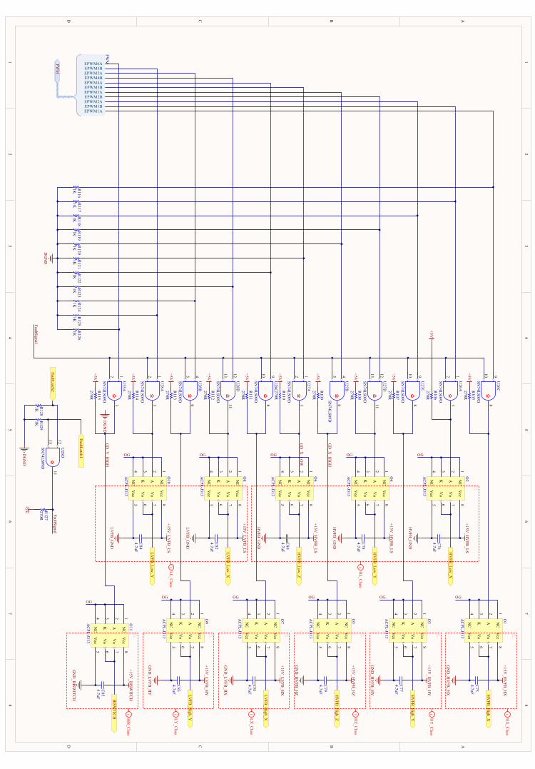
1 1
2 2
3 3
4 4
5 5
6 6
7 7
8 8
DD
CC
BB
AA
NC
1
A2
K3
NC
4V
ee5
Vo
6
Vo
7
Vcc
8O
2
AC
PL-J313
HV
FB_Low
_X
9108
U26C
SN74LS09D
9108
U27C
SN74LS09D
121311
U27D
SN74LS09D
456
U27B
SN74LS09D
123
U27A
SN74LS09D
123
U35A
SN74LS09D
121311
U26D
SN74LS09D
EPWM1AEPWM1BEPWM2AEPWM2BEPWM3AEPWM3BEPWM4AEPWM4BEPWM5AEPWM5BEPWM6A
PWM
PWM
DG
ND
+5V
+5V
+5V
+5V
+5V
+5V
+5V
+5V
+5V
+5V
+5V
HV
FB_G
ND
+15V_H
VFB
_LS
NC
1
A2
K3
NC
4V
ee5
Vo
6
Vo
7
Vcc
8O
1
AC
PL-J313
HV
FB_H
igh_X
GN
D_H
VFB
_HX
+15V_H
VFB
_HX
NC
1
A2
K3
NC
4V
ee5
Vo
6
Vo
7
Vcc
8O
3
AC
PL-J313
HV
FB_H
igh_Y
GN
D_H
VFB
_HY
+15V_H
VFB
_HY
NC
1
A2
K3
NC
4V
ee5
Vo
6
Vo
7
Vcc
8O
4
AC
PL-J313
HV
FB_Low
_Y
HV
FB_G
ND
+15V_H
VFB
_LS
NC
1
A2
K3
NC
4V
ee5
Vo
6
Vo
7
Vcc
8O
5
AC
PL-J313
HV
FB_H
igh_Z
GN
D_H
VFB
_HZ
+15V_H
VFB
_HZ
NC
1
A2
K3
NC
4V
ee5
Vo
6
Vo
7
Vcc
8O
6
AC
PL-J313
HV
FB_Low
_Z
HV
FB_G
ND
+15V_H
VFB
_LS
NC
1
A2
K3
NC
4V
ee5
Vo
6
Vo
7
Vcc
8O
7
AC
PL-J313
LVFB
_High_X
GN
D_LV
FB_H
X
+15V_LV
FB_H
X
NC
1
A2
K3
NC
4V
ee5
Vo
6
Vo
7
Vcc
8O
8
AC
PL-J313
LVFB
_Low_X
LVFB
_GN
D
+15V_LV
FB_LS
NC
1
A2
K3
NC
4V
ee5
Vo
6
Vo
7
Vcc
8O
9
AC
PL-J313
LVFB
_High_Y
GN
D_LV
FB_H
Y
+15V_LV
FB_H
Y
NC
1
A2
K3
NC
4V
ee5
Vo
6
Vo
7
Vcc
8O
10
AC
PL-J313
LVFB
_Low_Y
LVFB
_GN
D
+15V_LV
FB_LS
NC
1
A2
K3
NC
4V
ee5
Vo
6
Vo
7
Vcc
8O
11
AC
PL-J313
BISW
ITCH
GN
D_B
ISWITC
H
+15V_B
ISWITC
H
DG
ND
+5V
FaultLatch2
FaultLatch1
FaultSignal
FaultSignal
1K R116
1K R117
1K R118
1K R119
1K R120
1K R121
1K R122
1K R123
1K R124
1K R125
1K R126
1K R128
1K R129
4.7uFC
76
4.7uFC
75
4.7uFC
78
4.7uFC
77
4.7uFC
79
4.7uFC
80
4.7uFC
82
4.7uFC
81
4.7uFC
83
4.7uFC
84
4.7uFC
85
270RR
127
270R
R115
270R
R114
270R
R113
270R
R112
270R
R111
270R
R110
270R
R109
270R
R108
270R
R107
270R
R106
270R
R105
DG
ND
GD
_X_H
IGH
GD
_X_LO
W
GD
_Y_H
IGH
9108
U28C
SN74LS09D
121311
U28D
SN74LS09D
456
U28B
SN74LS09D
123
U28A
SN74LS09D
iH
X_C
lass
iH
L_Class
iH
Y_C
lass
iH
Z_Class
iLX
_Class
iLY
_Class
iLL_C
lass
iB
IS_Class
OG
OGOGOGOGOG
OG OG OGOG
OG
123
U26A
SN74LS09D
PIC7501 PIC7502COC75
PIC7601 PIC7602COC76
PIC7701 PIC7702COC77
PIC7801 PIC7802COC78
PIC7901 PIC7902COC79
PIC8001 PIC8002COC80
PIC8101 PIC8102COC81
PIC8201 PIC8202COC82
PIC8301 PIC8302COC83
PIC8401 PIC8402COC84
PIC8501 PIC8502COC85
PIO101
PIO102
PIO103
PIO104
PIO105
PIO106
PIO107
PIO108
COO1
PIO201
PIO202
PIO203
PIO204
PIO205
PIO206
PIO207
PIO208
COO2
PIO301
PIO302
PIO303
PIO304
PIO305
PIO306
PIO307
PIO308
COO3
PIO401
PIO402
PIO403
PIO404
PIO405
PIO406
PIO407
PIO408
COO4
PIO501
PIO502
PIO503
PIO504
PIO505
PIO506
PIO507
PIO508
COO5
PIO601
PIO602
PIO603
PIO604
PIO605
PIO606
PIO607
PIO608
COO6
PIO701
PIO702
PIO703
PIO704
PIO705
PIO706
PIO707
PIO708
COO7
PIO801
PIO802
PIO803
PIO804
PIO805
PIO806
PIO807
PIO808
COO8
PIO901
PIO902
PIO903
PIO904
PIO905
PIO906
PIO907
PIO908
COO9
PIO1001
PIO1002
PIO1003
PIO1004
PIO1005
PIO1006
PIO1007
PIO1008
COO10
PIO1101
PIO1102
PIO1103
PIO1104
PIO1105
PIO1106
PIO1107
PIO1108
COO11
PIR10501PIR10502 COR105
PIR10601PIR10602 COR106
PIR10701PIR10702 COR107
PIR10801PIR10802 COR108
PIR10901PIR10902 COR109
PIR11001PIR11002 COR110
PIR11101PIR11102 COR111
PIR11201PIR11202 COR112
PIR11301PIR11302 COR113
PIR11401PIR11402 COR114
PIR11501PIR11502 COR115
PIR11601 PIR11602COR116PIR11701 PIR11702COR117PIR11801 PIR11802COR118PIR11901 PIR11902COR119PIR12001 PIR12002COR120PIR12101 PIR12102COR121PIR12201 PIR12202COR122PIR12301 PIR12302COR123PIR12401 PIR12402COR124PIR12501 PIR12502COR125PIR12601 PIR12602COR126
PIR12701 PIR12702COR127
PIR12801 PIR12802COR128PIR12901 PIR12902COR129
PIU2601
PIU2602
PIU2603
COU26A
PIU2608
PIU2609
PIU26010 COU26C
PIU26011
PIU26012
PIU26013 COU26D
PIU2701
PIU2702
PIU2703
COU27A
PIU2704
PIU2705
PIU2706
COU27B
PIU2708
PIU2709
PIU27010 COU27C
PIU27011
PIU27012
PIU27013 COU27D
PIU2801
PIU2802
PIU2803
COU28A
PIU2804
PIU2805
PIU2806
COU28B
PIU2808
PIU2809
PIU28010 COU28C
PIU28011
PIU28012
PIU28013 COU28D
PIU3501
PIU3502
PIU3503
COU35A
POBISWITCH
POFAULTLATCH1
POFAULTLATCH2
POHVFB0HIGH0X
POHVFB0HIGH0Y
POHVFB0HIGH0Z
POHVFB0LOW0X
POHVFB0LOW0Y
POHVFB0LOW0Z
POLVFB0HIGH0X
POLVFB0HIGH0Y
POLVFB0LOW0X
POLVFB0LOW0Y
POPWM
POPWM0EPWM1APOPWM0EPWM1BPOPWM0EPWM2APOPWM0EPWM2BPOPWM0EPWM3APOPWM0EPWM3BPOPWM0EPWM4APOPWM0EPWM4BPOPWM0EPWM5APOPWM0EPWM5BPOPWM0EPWM6A
Fusion
Font monospazio
Gate Drivers Schematic A1.4
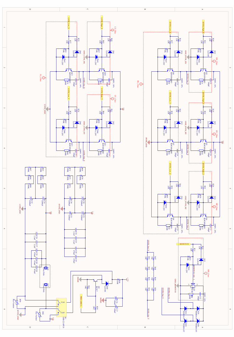
1 1
2 2
3 3
4 4
5 5
6 6
7 7
8 8
DD
CC
BB
AA
D26
Vz 20V
D37
Vz 20V
D27
Vz 20V
D38
Vz 20V
D28
Vz 20V
D39
Vz 20V
D43
Vz 20V
D47
Vz 20V
D44
Vz 20V
D48
Vz 20V
HV
FB_H
igh_X
HV
FB_Low
_X
HV
FB_H
igh_Y
HV
FB_Low
_Y
HV
FB_H
igh_Z
HV
FB_Low
_Z
LVFB
_High_X
LVFB
_High_Y
LVFB
_Low_X
LVFB
_Low_Y
HV
FB_G
ND
LVFB
_GN
D
Vdc
Vfc
Vfc
LVFB
_GN
D
HV
FB_G
ND Vdc
D31
Vz 20V
BISWITCH
GN
D_B
ISWITC
H
GN
D_H
VFB
_HX
GN
D_H
VFB
_HY
GN
D_H
VFB
_HZ
GN
D_LV
FB_H
XG
ND
_LVFB
_HY
HV
FB_O
ut_XH
VFB
_Out_Y
HV
FB_O
ut_Z
LVFB
_Out_X
LVFB
_Out_Y
HV
FB_O
ut_X
HV
FB_O
ut_Y
HV
FB_O
ut_ZH
VFB
_Out_X
750
R47
750
R48
750
R49
750
R53
750
R52
750
R51
750
R50
750
R54
PREC
AR
ICA
HV
FB_G
ND Vdc
Q9
BC
817
DG
ND 220R
R46
+17V
3
1
2
Q5
FCB
11N60
22R
R21
22R
R18
22R
R1922R
R22
22R
R2022R
R23
22R
R3622R
R39
22R
R3522R
R38
22R
R3422R
R37
D22
LL4148
D34
LL4148
D35
LL4148
D23
LL4148
D24
LL4148
D36
LL4148
22R
R6022R
R63
22R
R6122R
R64
22R
R7622R
R78
22R
R77
22R
R75
D41
LL4148
D42
LL4148
D46
LL4148
D45
LL4148
10KR
2810KR
2910KR
30
10KR
4510KR
4410KR
43
10KR
81
10KR
6710KR
68
10KR
82
D25
LL414822R
R2422R
R31
10KR
33
10K
R62
300KR
69300KR
70300KR
71
300KR
74300KR
73300KR
72
300KR
83300KR
84300KR
85
300KR
89300KR
88300KR
872200uFC
42
2200uFC
34
2200uFC
202200uFC
21
2200uFC
302200uFC
31
R90
Res V
aristor
R86
Res V
aristor
DG
ND
470nFC
25470nFC
24470nFC
39470nFC
40470nFC
41
100RR
40
100RR
25100RR
26
100RR
41100RR
42
100RR
27
100RR
66100RR
65
100RR
79100RR
80
1000V, 10%
100pFC
13
1000V, 10%
100pFC
9
1000V, 10%
100pFC
10
1000V, 10%
100pFC
14
1000V, 10%
100pFC
15
1000V, 10%
100pFC
11
1000V, 10%
100pFC
19
1000V, 10%
100pFC
18
1000V, 10%
100pFC
32
1000V, 10%
100pFC
33
D40
LL4148
1000V, 10%
100pFC
12
100RR
32
2.2uFC
36
2.2uFC
222.2uFC
23
2.2uFC
37
2K2
R59
Q2
IKW
30N60H
3
Q6
IKW
30N60H
3
Q3
IKW
30N60H
3
Q7
IKW
30N60H
3Q
8IK
W30N
60H3
Q4
IKW
30N60H
3
Q10
IKW
30N60H
3
Q12
IKW
30N60H
3Q
13IK
W30N
60H3
Q11
IKW
30N60H
3
BISW
ITCH
_GD
100uFC
16100uFC
17
U17
Power H
ole
U16
Power H
ole
Coil+
Coil-
K1
G6B
-2214PUS
D29
FESB16-JT
D30
FESB16-JT
D33
FESB16-JT
D32
FESB16-JT
iH
X_C
lassi
HY
_Class
iH
Z_Class
iH
L_Class
iB
IS_Class
iLX
_Class
iLY
_Class
iLL_C
lass
PIC901 PIC902COC9
PIC1001 PIC1002COC10
PIC1101 PIC1102COC11
PIC1201 PIC1202COC12
PIC1301 PIC1302COC13
PIC1401 PIC1402COC14
PIC1501 PIC1502COC15
PIC1601PIC1602
COC16PIC1701PIC1702
COC17
PIC1801 PIC1802COC18
PIC1901 PIC1902COC19
PIC2001PIC2002
COC20PIC2101PIC2102
COC21
PIC2201 PIC2202COC22
PIC2301 PIC2302COC23
PIC2401 PIC2402COC24
PIC2501 PIC2502COC25
PIC3001PIC3002
COC30PIC3101PIC3102
COC31PIC3201 PIC3202
COC32PIC3301 PIC3302
COC33
PIC3401PIC3402
COC34
PIC3601 PIC3602COC36
PIC3701 PIC3702COC37
PIC3901 PIC3902COC39
PIC4001 PIC4002COC40
PIC4101 PIC4102COC41
PIC4201PIC4202
COC42
PID2201
PID2202 COD22
PID2301
PID2302 COD23
PID2401
PID2402 COD24
PID2501
PID2502 COD25
PID2601 PID2602COD26
PID2701 PID2702COD27
PID2801 PID2802COD28
PID2901PID2903 PID2904COD29
PID3001PID3003 PID3004COD30
PID3101 PID3102COD31
PID3201PID3203 PID3204COD32
PID3301PID3303 PID3304COD33
PID3401
PID3402 COD34
PID3501
PID3502 COD35
PID3601
PID3602 COD36
PID3701 PID3702COD37
PID3801 PID3802COD38
PID3901 PID3902COD39
PID4001 PID4002COD40
PID4101
PID4102 COD41
PID4201
PID4202 COD42
PID4301 PID4302COD43
PID4401 PID4402COD44
PID4501
PID4502 COD45
PID4601
PID4602 COD46
PID4701 PID4702COD47
PID4801 PID4802COD48
PIK101
PIK103PIK104
PIK105PIK106
PIK108COK1
PIQ201
PIQ202PIQ203 COQ2
PIQ301
PIQ302PIQ303 COQ3
PIQ401
PIQ402PIQ403 COQ4
PIQ501
PIQ502PIQ503COQ5
PIQ601
PIQ602PIQ603 COQ6
PIQ701
PIQ702PIQ703 COQ7
PIQ801
PIQ802PIQ803 COQ8
PIQ901
PIQ902 PIQ903COQ9
PIQ1001
PIQ1002PIQ1003 COQ10
PIQ1101
PIQ1102PIQ1103 COQ11
PIQ1201
PIQ1202PIQ1203 COQ12
PIQ1301
PIQ1302PIQ1303 COQ13
PIR1801PIR1802
COR18PIR1901
PIR1902COR19
PIR2001PIR2002
COR20
PIR2101PIR2102
COR21PIR2201
PIR2202COR22
PIR2301PIR2302
COR23
PIR2401PIR2402
COR24
PIR2501 PIR2502COR25
PIR2601 PIR2602COR26
PIR2701 PIR2702COR27
PIR2801 PIR2802COR28
PIR2901 PIR2902COR29
PIR3001 PIR3002COR30
PIR3101PIR3102
COR31
PIR3201 PIR3202COR32
PIR3301 PIR3302COR33
PIR3401PIR3402
COR34PIR3501
PIR3502COR35
PIR3601PIR3602
COR36
PIR3701PIR3702
COR37PIR3801
PIR3802COR38
PIR3901PIR3902
COR39
PIR4001 PIR4002COR40
PIR4101 PIR4102COR41
PIR4201 PIR4202COR42
PIR4301 PIR4302COR43
PIR4401 PIR4402COR44
PIR4501 PIR4502COR45
PIR4601 PIR4602COR46
PIR4701PIR4702
COR47PIR4801
PIR4802COR48
PIR4901PIR4902
COR49PIR5001
PIR5002COR50
PIR5101PIR5102
COR51PIR5201
PIR5202COR52
PIR5301PIR5302
COR53PIR5401
PIR5402COR54
PIR5901PIR5902
COR59
PIR6001PIR6002
COR60PIR6101
PIR6102COR61
PIR6201PIR6202 COR62
PIR6301PIR6302
COR63PIR6401
PIR6402COR64
PIR6501 PIR6502COR65
PIR6601 PIR6602COR66
PIR6701 PIR6702COR67
PIR6801 PIR6802COR68
PIR6901 PIR6902COR69
PIR7001 PIR7002COR70
PIR7101 PIR7102COR71
PIR7201 PIR7202COR72
PIR7301 PIR7302COR73
PIR7401 PIR7402COR74
PIR7501PIR7502
COR75PIR7601
PIR7602COR76
PIR7701PIR7702
COR77PIR7801
PIR7802COR78
PIR7901 PIR7902COR79
PIR8001 PIR8002COR80
PIR8101 PIR8102COR81
PIR8201 PIR8202COR82
PIR8301 PIR8302COR83
PIR8401 PIR8402COR84
PIR8501 PIR8502COR85
PIR8601PIR8602
COR86
PIR8701 PIR8702COR87
PIR8801 PIR8802COR88
PIR8901 PIR8902COR89
PIR9001PIR9002
COR90
PIU1601 COU16
PIU1701
COU17
POBISWITCH
POHVFB0HIGH0X
POHVFB0HIGH0Y
POHVFB0HIGH0Z
POHVFB0LOW0X
POHVFB0LOW0Y
POHVFB0LOW0Z
POLVFB0HIGH0X
POLVFB0HIGH0Y
POLVFB0LOW0X
POLVFB0LOW0Y
POPRECARICA
Fusion
Font monospazio
Power Circuit Schematic A1.5
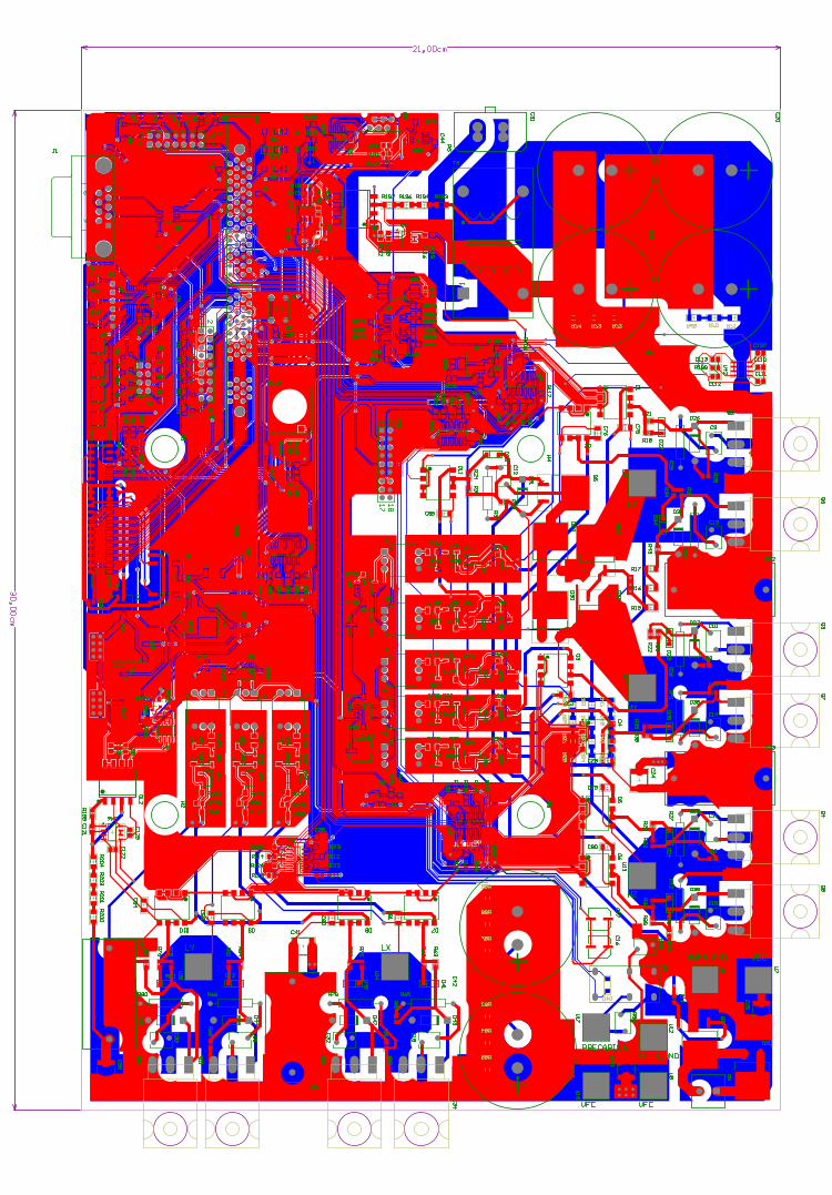
PAC102PAC101COC1
PAC202PAC201COC2
PAC302PAC301COC3
PAC402PAC401
COC4PAC502
PAC501COC5
PAC602
PAC601
COC6
PAC702PAC701
COC7
PAC802PAC801
COC8
PAC901PAC902
COC9PAC1001
PAC1002COC10
PAC1101PAC1102
COC11
PAC1201PAC1202
COC12
PAC1301PAC1302
COC13PAC1401
PAC1402COC14
PAC1501PAC1502
COC15
PAC1601PAC1602
COC16
PAC1701PAC1702
COC17
PAC1801PAC1802
COC18
PAC1901PAC1902
COC19
PAC2002
PAC2001
COC20
PAC2102
PAC2101
COC21
PAC2201
PAC2202COC22
PAC2301
PAC2302COC23
PAC2402PAC2401
COC24
PAC2502PAC2501
COC25
PAC2602
PAC2601
COC26
PAC2702PAC2701
COC27
PAC2802
PAC2801
COC28
PAC2902PAC2901COC29
PAC3002
PAC3001
COC30
PAC3102
PAC3101
COC31
PAC3201
PAC3202
COC32PAC3301
PAC3302
COC33
PAC3402PAC3401
COC34
PAC3502PAC3501
COC35
PAC3601PAC3602
COC36
PAC3701PAC3702
COC37
PAC3802PAC3801
COC38
PAC3902PAC3901
COC39 PAC4002PAC4001COC40
PAC4102
PAC4101COC41
PAC4202PAC4201
COC42
PAC4302PAC4301
COC43
PAC4402PAC4401
COC44
PAC4502PAC4501
COC45
PAC5402
PAC5401
COC54
PAC5502PAC5501
COC55
PAC6102 PAC6101COC61
PAC6202
PAC6201
COC62
PAC6302 PAC6301COC63
PAC6402PAC6401
COC64
PAC7502
PAC7501
COC75
PAC7602PAC7601
COC76
PAC7702
PAC7701COC77
PAC7802
PAC7801
COC78
PAC7902
PAC7901
COC79
PAC8002
PAC8001
COC80
PAC8102PAC8101
COC81
PAC8202PAC8201
COC82
PAC8302PAC8301
COC83
PAC8402PAC8401
COC84
PAC8502
PAC8501
COC85
PAC9302
PAC9301COC93
PAC10002PAC10001
COC100
PAC10102PAC10101
COC101
PAC10302PAC10301
COC103
PAC10402PAC10401
COC104
PAC10502PAC10501COC105
PAC10602PAC10601
COC106
PAC10702PAC10701
COC107
PAC10802PAC10801COC108
PAC10902PAC10901 COC109
PAC11002PAC11001
COC110PAC11102PAC11101
COC111PAC11202PAC11201 COC112
PAC11302PAC11301
COC113
PAC11402PAC11401
COC114
PAC11502PAC11501
COC115
PAC11602PAC11601COC116
PAC11702
PAC11701
COC117 PAC11802
PAC11801 COC118
PAC11902PAC11901COC119
PAC12002PAC12001COC120
PAC12102PAC12101COC121
PAC12202PAC12201
COC122
PAC12302PAC12301
COC123
PAC12402
PAC12401
COC124PAC12502PAC12501
COC125
PAC14702
PAC14701COC147
PAC14802PAC14801
COC148
PAC14902
PAC14901COC149
PAC15002
PAC15001COC150
PAC15102PAC15101
COC151PAC15202
PAC15201COC152
PAC15301 PAC15302COC153
PAC15402PAC15401
COC154
PAC15502
PAC15501COC155
PAC15602PAC15601
COC156PAC15702
PAC15701COC157
PAC15802PAC15801
COC158
PAC15902
PAC15901
COC159
PAC16002PAC16001
COC160
PAC16102PAC16101 COC161
PAC16202
PAC16201
COC162
PAC16302PAC16301
COC163
PAC16401PAC16402
COC164
PAC16502PAC16501
COC165
PAC16602PAC16601
COC166
PAC16702
PAC16701
COC167
PAC16802PAC16801
COC168
PAC16902
PAC16901COC169
PAC17002PAC17001
COC170
PAC17102
PAC17101COC171PAC17201 PAC17202
COC172PAC17302PAC17301
COC173
PAD103PAD102PAD101
COD1
PAD203
PAD202
PAD201
COD2
PAD303PAD302PAD301
COD3
PAD403PAD402
PAD401
COD4
PAD503PAD502PAD501
COD5
PAD603PAD602
PAD601
COD6
PAD703PAD702PAD701
COD7PAD803
PAD802
PAD801
COD8
PAD903PAD902PAD901
COD9
PAD1003PAD1002PAD1001
COD10
PAD1103PAD1102PAD1101
COD11
PAD1201
PAD1202COD12PAD1301
PAD1302COD13PAD1401
PAD1402COD14
PAD1503PAD1502PAD1501
COD15
PAD1603PAD1602PAD1601
COD16
PAD1703PAD1702PAD1701
COD17PAD1803PAD1802PAD1801
COD18
PAD1903PAD1902PAD1901
COD19
PAD2003PAD2002PAD2001
COD20
PAD2101
PAD2103 PAD2104COD21
PAD2201PAD2202
COD22
PAD2301PAD2302
COD23PAD2401
PAD2402COD24
PAD2501
PAD2502
COD25
PAD2601PAD2602
COD26PAD2701
PAD2702COD27
PAD2801PAD2802
COD28
PAD2901
PAD2903
PAD2904COD29
PAD3001
PAD3003
PAD3004COD30
PAD3101PAD3102COD31
PAD3201
PAD3203
PAD3204COD32
PAD3301
PAD3303 PAD3304COD33
PAD3401PAD3402
COD34
PAD3501PAD3502
COD35
PAD3601PAD3602
COD36
PAD3701PAD3702
COD37
PAD3801PAD3802
COD38PAD3901
PAD3902COD39
PAD4001PAD4002
COD40
PAD4101
PAD4102
COD41
PAD4201
PAD4202COD42
PAD4301
PAD4302COD43
PAD4401
PAD4402COD44
PAD4501
PAD4502
COD45
PAD4601
PAD4602
COD46
PAD4701
PAD4702COD47
PAD4801
PAD4802
COD48
PAD4901 PAD4902COD49
PAD5001
PAD5002COD50
PAD5903PAD5902
PAD5901COD59
PAD6303
PAD6302
PAD6301COD63
PAD6403PAD6402
PAD6401
COD64
PAD6503
PAD6502PAD6501
COD65
PAD7101 PAD7102
COD71
PAD7201 PAD7202COD72PAD7301 PAD7302
COD73
PAD7401 PAD7402COD74
PAD7501 PAD7502COD75
PAD7601 PAD7602COD76
PAD7701PAD7702
COD77
PAD7801PAD7802
COD78
PAD7901PAD7902
COD79
PAD8001PAD8002
COD80
PAD8101PAD8102
COD81
PAD8201PAD8202
COD82
PAD8301 PAD8302COD83
PAD8401 PAD8402COD84
PADS101PADS103
PADS105PADS107
PADS109PADS1011
PADS1013PADS1015
PADS1021PADS1019
PADS1017PADS1033
PADS1035PADS1037
PADS1031PADS1029
PADS1027PADS1025
PADS1023PADS1039
PADS1041PADS1043
PADS1049PADS1047
PADS1045
PADS1046PADS1048
PADS1050PADS1044
PADS1042PADS1040
PADS1024PADS1026
PADS1028PADS1030
PADS1032PADS1038
PADS1036PADS1034
PADS1018PADS1020
PADS1022PADS1016
PADS1014PADS1012
PADS1010PADS108
PADS106PADS104
PADS102
PADS1052PADS1054
PADS1056PADS1058
PADS1060PADS1062
PADS1064PADS1066
PADS1072PADS1070
PADS1068PADS1084
PADS1086PADS1088
PADS1082PADS1080
PADS1078PADS1076
PADS1074PADS1090
PADS1092PADS1094
PADS10100PADS1098
PADS1096PADS1095PADS1097
PADS1099PADS1093
PADS1091PADS1089
PADS1073PADS1075
PADS1077PADS1079
PADS1081PADS1087
PADS1085PADS1083
PADS1067PADS1069
PADS1071PADS1065
PADS1063PADS1061
PADS1059PADS1057
PADS1055PADS1053
PADS1051
CODS1
PAH101
COH1
PAH201
COH2 PAH301COH3
PAH401 COH4
PAJ1011PAJ1010
PAJ101
PAJ106
PAJ102
PAJ107
PAJ103
PAJ108
PAJ104
PAJ109
PAJ105
COJ1
PAK106
PAK105
PAK108
PAK104
PAK103
PAK101
COK1
PAO105PAO106
PAO107PAO108
PAO104PAO103
PAO102PAO101
COO1
PAO205PAO206
PAO207
PAO208
PAO204PAO203
PAO202
PAO201COO2
PAO305PAO306
PAO307PAO308
PAO304PAO303
PAO302PAO301
COO3
PAO405PAO406
PAO407PAO408
PAO404PAO403
PAO402PAO401
COO4PAO505
PAO506PAO507
PAO508
PAO504PAO503
PAO502PAO501
COO5PAO605
PAO606PAO607
PAO608
PAO604PAO603
PAO602PAO601
COO6
PAO705
PAO706
PAO707PAO708
PAO704
PAO703
PAO702PAO701
COO7
PAO805PAO806
PAO807
PAO808
PAO804PAO803
PAO802
PAO801COO8
PAO905PAO906
PAO907
PAO908
PAO904PAO903
PAO902
PAO901COO9
PAO1005PAO1006
PAO1007
PAO1008
PAO1004PAO1003
PAO1002
PAO1001COO10
PAO1105PAO1106
PAO1107PAO1108
PAO1104PAO1103
PAO1102PAO1101
COO11
PAOL108PAOL107
PAOL106PAOL105 PAOL104
PAOL103PAOL102PAOL101
COOL1
PAOL208
PAOL207
PAOL206
PAOL205PAOL204
PAOL203
PAOL202
PAOL201
COOL2PAP108
PAP107
PAP106
PAP105
PAP104
PAP103
PAP102
PAP101
COP1
PAP201PAP202
PAP203PAP204
PAP205PAP206
COP2
PAP301
PAP3018
PAP3017
PAP3016
PAP3015
PAP3014
PAP3013
PAP3012
PAP3011
PAP3010
PAP309
PAP308
PAP307
PAP306
PAP305
PAP304
PAP303
PAP302COP3
PAP401PAP402 PAP403PAP404 PAP405PAP406 PAP407PAP408 PAP409PAP4010 PAP4011PAP4012 PAP4013PAP4014
COP4
PAP502
PAP501
COP5
PAP602 PAP601
PAP604
PAP603
COP6
PAP800 PAP803
PAP801
PAP805
PAP802
PAP804
PAP806
COP8
PAP903PAP904 PAP901PAP907PAP905
PAP9017PAP9015PAP909
PAP9013PAP9011PAP9012PAP9014
PAP9010PAP9016
PAP9019PAP9018PAP906
PAP908PAP902
PAP9040PAP9032
PAP9034PAP9036
PAP9038PAP9028PAP9026PAP9024PAP9022
PAP9030 PAP9029PAP9021
PAP9023PAP9025
PAP9027PAP9037PAP9035PAP9033PAP9031
PAP9039
PAP9020
COP9
PAP1101PAP11018PAP11017
PAP11016PAP11015
PAP11014PAP11013
PAP11012PAP11011
PAP11010PAP1109
PAP1108PAP1107
PAP1106PAP1105
PAP1104PAP1103
PAP1102
COP11
PAQ101
PAQ103 PAQ104
COQ1
PAQ201PAQ202
PAQ203COQ2
PAQ301PAQ302
PAQ303
COQ3
PAQ401PAQ402
PAQ403
COQ4
PAQ501PAQ503
PAQ504COQ5
PAQ601PAQ602
PAQ603
COQ6
PAQ701PAQ702
PAQ703
COQ7
PAQ801PAQ802
PAQ803
COQ8
PAQ903PAQ902
PAQ901COQ9
PAQ1001
PAQ1002
PAQ1003
COQ10
PAQ1101
PAQ1102
PAQ1103COQ11
PAQ1201
PAQ1202
PAQ1203COQ12
PAQ1301
PAQ1302
PAQ1303
COQ13
PAQ1403
PAQ1402PAQ1401
COQ14
PAQ1501PAQ1502
PAQ1503PAQ1504
COQ15
PAR102
PAR101COR1
PAR202
PAR201COR2
PAR302
PAR301
COR3PAR402
PAR401
COR4
PAR502
PAR501
COR5
PAR602
PAR601
COR6
PAR702
PAR701
COR7
PAR802PAR801COR8
PAR902PAR901COR9PAR1002PAR1001COR10
PAR1102PAR1101
COR11 PAR1202
PAR1201
COR12
PAR1302PAR1301
COR13
PAR1402PAR1401
COR14
PAR1502
PAR1501
COR15
PAR1602
PAR1601
COR16
PAR1702
PAR1701
COR17
PAR1802
PAR1801 COR18PAR1902PAR1901
COR19
PAR2002PAR2001
COR20
PAR2102
PAR2101COR21
PAR2202PAR2201COR22
PAR2302PAR2301
COR23
PAR2402PAR2401
COR24
PAR2501PAR2502
COR25
PAR2601PAR2602
COR26
PAR2701PAR2702
COR27
PAR2802
PAR2801
COR28
PAR2902
PAR2901COR29
PAR3002
PAR3001COR30
PAR3102PAR3101
COR31
PAR3201PAR3202
COR32PAR3302
PAR3301
COR33
PAR3402PAR3401
COR34
PAR3502
PAR3501
COR35
PAR3602PAR3601
COR36
PAR3702PAR3701
COR37
PAR3802
PAR3801
COR38
PAR3902PAR3901
COR39
PAR4001PAR4002
COR40PAR4101
PAR4102
COR41
PAR4201PAR4202
COR42
PAR4302PAR4301COR43
PAR4402
PAR4401COR44
PAR4502PAR4501COR45
PAR4602
PAR4601
COR46
PAR4702PAR4701
COR47
PAR4802PAR4801
COR48
PAR4902PAR4901
COR49
PAR5002PAR5001
COR50
PAR5102PAR5101COR51
PAR5202PAR5201COR52
PAR5302PAR5301COR53
PAR5402PAR5401COR54
PAR5502PAR5501COR55
PAR5602PAR5601COR56
PAR5702PAR5701COR57
PAR5802PAR5801COR58
PAR5902PAR5901COR59
PAR6002PAR6001
COR60
PAR6102PAR6101
COR61
PAR6202PAR6201COR62
PAR6302PAR6301
COR63
PAR6402PAR6401
COR64
PAR6501
PAR6502
COR65
PAR6601
PAR6602
COR66
PAR6702PAR6701
COR67
PAR6802PAR6801COR68
PAR6902
PAR6901 COR69
PAR7002
PAR7001COR70
PAR7102
PAR7101 COR71
PAR7202
PAR7201 COR72
PAR7302
PAR7301COR73
PAR7402
PAR7401 COR74
PAR7502PAR7501
COR75
PAR7602PAR7601
COR76
PAR7702PAR7701
COR77
PAR7802PAR7801
COR78
PAR7901
PAR7902COR79
PAR8001
PAR8002
COR80
PAR8102PAR8101COR81
PAR8202PAR8201
COR82
PAR8302PAR8301
COR83PAR8402
PAR8401COR84
PAR8502PAR8501
COR85
PAR8601PAR8602
COR86
PAR8702PAR8701
COR87PAR8802
PAR8801COR88
PAR8902PAR8901
COR89
PAR9001
PAR9002
COR90
PAR9102PAR9101
COR91
PAR9202PAR9201
COR92
PAR9302PAR9301COR93
PAR9402PAR9401 COR94
PAR9502PAR9501
COR95PAR9602
PAR9601COR96
PAR9702
PAR9701COR97
PAR9802
PAR9801
COR98
PAR9902PAR9901
COR99
PAR10002
PAR10001
COR100PAR10102
PAR10101
COR101
PAR10201PAR10202
COR102
PAR10301
PAR10302COR103
PAR10401PAR10402 COR104
PAR10502PAR10501
COR105
PAR10602PAR10601COR106
PAR10702PAR10701COR107
PAR10802PAR10801COR108
PAR10902PAR10901COR109
PAR11002PAR11001
COR110
PAR11102
PAR11101
COR111PAR11202
PAR11201
COR112
PAR11302
PAR11301
COR113PAR11402
PAR11401
COR114
PAR11502PAR11501COR115 PAR11601
PAR11602COR116
PAR11701PAR11702COR117
PAR11801PAR11802COR118
PAR11901PAR11902COR119
PAR12001PAR12002
COR120
PAR12101PAR12102
COR121
PAR12201
PAR12202
COR122PAR12301
PAR12302
COR123
PAR12401
PAR12402
COR124PAR12501
PAR12502
COR125
PAR12601PAR12602COR126
PAR12702PAR12701
COR127 PAR12801PAR12802
COR128
PAR12901PAR12902
COR129
PAR13001
PAR13002COR130
PAR13101PAR13102
COR131PAR13201
PAR13202COR132
PAR13302PAR13301
COR133PAR13402
PAR13401COR134
PAR15002
PAR15001COR150
PAR15202PAR15201COR152
PAR15702PAR15701
COR157
PAR16802PAR16801
COR168PAR16902PAR16901
COR169
PAR17202
PAR17201PAR1720
COR172PAR17502
PAR17501COR175
PAR17602PAR17601
COR176
PAR17702
PAR17701
COR177
PAR17802
PAR17801
COR178
PAR17902
PAR17901
COR179
PAR18002PAR18001COR180
PAR18102PAR18101COR181
PAR18202
PAR18201
COR182PAR18302
PAR18301
COR183PAR18402
PAR18401
COR184
PAR18502PAR18501COR185
PAR18602PAR18601
COR186
PAR18702PAR18701COR187
PAR18802
PAR18801
COR188
PAR18902PAR18901
COR189
PAR19002
PAR19001
COR190
PAR19102
PAR19101
COR191
PAR19202PAR19201COR192
PAR19301
PAR19302
COR193PAR19401
PAR19402
COR194
PAR19502PAR19501
COR195 PAR19601
PAR19602
COR196
PAR19701
PAR19702
COR197
PAR19802PAR19801COR198
PAR19902PAR19901COR199
PAR20001PAR20002
COR200
PAR20101PAR20102
COR201
PAR20202PAR20201
COR202
PAR20301PAR20302
COR203
PAR20401PAR20402
COR204
PAR23902
PAR23901COR239
PAR24002PAR24001
COR240
PAR24102
PAR24101COR241
PAR24202PAR24201
COR242PAR24302PAR24301
COR243
PAR24402
PAR24401COR244
PAR24502PAR24501
COR245
PAR24602PAR24601
COR246
PAR24702
PAR24701
COR247PAR24802PAR24801
COR248
PAR24902
PAR24901
COR249PAR25002PAR25001COR250
PAR25102PAR25101
COR251
PAR25202
PAR25201
COR252PAR25302
PAR25301
COR253
PAR25402PAR25401
COR254
PAR25502PAR25501
COR255
PAS101
PAS102
COS1
PAT104PAT105
PAT106
PAT103PAT102
PAT101COT1
PAT201PAT202
PAT204PAT203COT2
PAT304
PAT302PAT303
PAT301COT3
PAT403
PAT402
PAT404
PAT401
COT4
PAT501PAT502
PAT504PAT503COT5
PAT601PAT602PAT603
PAT606PAT605PAT604
COT6PAT701PAT702
PAT703
PAT706PAT705PAT704
COT7PAT801PAT802
PAT803
PAT806PAT805PAT804
COT8
PAT901
PAT902
PAT903
PAT906
PAT905
PAT904
COT9
PAT1001
PAT1002
PAT1003
PAT1006
PAT1005
PAT1004
COT10
PAT1101
PAT1102
PAT1103
PAT1106
PAT1105
PAT1104
COT11
PAT1201PAT1202PAT1203
PAT1206PAT1205PAT1204
COT12
PAU105PAU106PAU107PAU108
PAU104PAU103PAU102PAU101COU1
PAU201
PAU202PAU203
PAU204PAU205
PAU206PAU207
PAU208PAU209
PAU2010
PAU2020
PAU2019PAU2018
PAU2017PAU2016
PAU2015PAU2014
PAU2013PAU2012
PAU2011
COU2
PAU301COU3
PAU401COU4
PAU501COU5
PAU601COU6
PAU701COU7
PAU801COU8
PAU901COU9
PAU1001COU10
PAU1101COU11
PAU1201COU12
PAU1301COU13
PAU1401COU14
PAU1501COU15
PAU1601COU16
PAU1701COU17
PAU1801PAU1802
PAU1803PAU1804
PAU1808PAU1807
PAU1806PAU1805
COU18
PAU1904PAU1903
PAU1901
PAU1902
COU19
PAU2001PAU2004
PAU2003
COU20
PAU2101PAU2103
PAU2104
COU21
PAU2201
PAU2203PAU2204
COU22
PAU2608
PAU2609
PAU26010
PAU26011
PAU26012
PAU26013
PAU26014
PAU2607
PAU2606
PAU2605
PAU2604
PAU2603
PAU2602
PAU2601
COU26
PAU2708
PAU2709
PAU27010
PAU27011
PAU27012PAU27013
PAU27014
PAU2707
PAU2706
PAU2705
PAU2704
PAU2703PAU2702
PAU2701
COU27
PAU2801 PAU28014PAU28013
PAU2804PAU2805PAU2802PAU2803
PAU2806PAU2807
PAU28012PAU28011PAU2808
PAU28010PAU2809
COU28
PAU3401
PAU3402PAU3403
PAU3404
PAU3408
PAU3407PAU3406
PAU3405
COU34
PAU3508
PAU3509
PAU35010
PAU35011
PAU35012
PAU35013
PAU35014
PAU3507
PAU3506
PAU3505
PAU3504
PAU3503
PAU3502
PAU3501
COU35
PAU3909
PAU39010PAU39011
PAU39012
PAU39013
PAU39014
PAU39015
PAU39016
PAU3908
PAU3907PAU3906
PAU3905
PAU3904
PAU3903
PAU3902
PAU3901
COU39
PAU4008PAU4009
PAU40010PAU40011
PAU40012PAU40013
PAU40014
PAU4007PAU4006
PAU4005PAU4004
PAU4003PAU4002
PAU4001COU40
PAU4101PAU4102PAU4104PAU4103
COU41
PAU4201PAU4202
PAU4203PAU4204
PAU4208PAU4207
PAU4206PAU4205COU42
PAU4301PAU4302PAU4303PAU4304
PAU4308PAU4307PAU4306PAU4305
COU43
PAU4401PAU4402
PAU4403
PAU4404
PAU4408PAU4407
PAU4406
PAU4405
COU44
PAU4501
PAU4502
PAU4503
PAU4504
PAU4508
PAU4507
PAU4506
PAU4505
COU45
PAU4601PAU4602PAU4603PAU4604
PAU4608PAU4607PAU4606PAU4605COU46
PAU5304PAU5303
PAU5301
PAU5302
COU53
PAU5401PAU5402PAU5403PAU5404
PAU5408PAU5407PAU5406PAU5405
COU54
PAU5504PAU5503
PAU5501
PAU5502
COU55PAU5604
PAU5603
PAU5601
PAU5602
COU56
PAU5704PAU5703
PAU5701
PAU5702
COU57
PAU5801PAU5802
PAU5803
PAU5804
PAU5808PAU5807
PAU5806
PAU5805
COU58PAU5904PAU5903
PAU5901PAU5902
COU59
PAU6004PAU6003PAU6001
PAU6002
COU60
PAU6101PAU6102PAU6103PAU6104
PAU6108PAU6107PAU6106PAU6105
COU61
PAU6204PAU6203
PAU6201
PAU6202
COU62
Fusion
Font monospazio
Power Card PCB A1.6
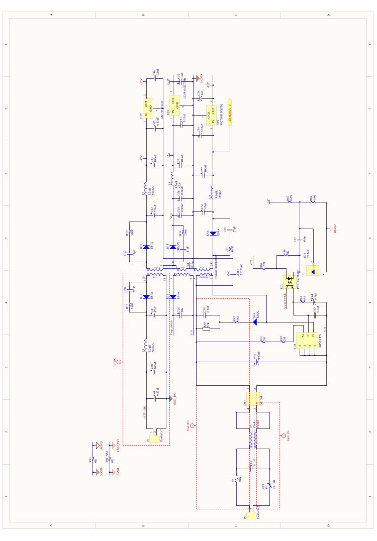
11
22
33
44
55
66
77
88
DD
CC
BB
AA
Vsu
p_sw
itch
Vsu
p_sw
itch
V_0 V
_0
+17V
+15V
+5V
IN1
4
OU
T3
GN
D
U18
LD29
150D
T33R
+3.3
V
IN4
1
OU
T3
GN
D
U19
MC
79M
15C
DTG
-15V
GN
D_I
SO
VC
5
+5V
DG
ND
10u
C48
0.1u
FC
65
6R8
R88
137R
R84
1KR86
4k99
R87
4k99
R89
680n
C63
6.8n
FC
58
27pF
C39
220u
FC
42
0.33
uFC
53
0.33
uFC
450.
33uF
C44
0.1u
FC
46
S S S S
M C D
U21
TOP2
5x-P
N
27K
R80
7R5
R82
250
VA
C2.
2nF
C60
IN1
4
OU
T3
GN
D
U17
MC
7815
CD
2T
3.3u
H58
0mA
L2
3.3u
H58
0mA
L4
0.33
uFC
541u
FC
55
10uF
C52
1 2
P4 Hea
der1
x20.
1uF
C61
F2 Fuse
3.3u
H58
0mA
L1
t°RT1
CL
170
10m
H
T5 Cho
ke10
0uF
C62
27pF
C38
27pF
C59
47pF
C47
270R
R79
390R
R81
390R
R78
390R
R77
3.3u
H3.
3AL3
1500
uFC
5015
00uF
C49
100u
FC
40
100u
FC
57
100u
FC
51
100u
FC
4347
uFC
41
47uF
C56
47uF
C64
VC
5
2MR85
2MR83
DG
ND
U20
PC81
7XJ0
000F
4
53
U22
TL34
1
13
1461311
84
Primario
12 -17V+17V
+17V
+5V
75
10 0V
T4 Flyb
ackT
rans
form
er
D13
ES1A
D16
ES1A
D12
ES1A
D14
ES1A
D18
ES3X
D15
ES3X
AN
ALO
GV
-17
1 2
P3 Hea
der1
x2
+17V
_ISO
+1
-2
~4
~3
D17
DF1
0M
iG
rid_I
N+
iG
rid_I
N-
0RR90
0RR91
_NM
DG
ND
AG
ND
DG
ND
GN
D_I
SOi
17_I
SO
PIC3801
PIC3802
COC3
8
PIC3901
PIC3902
COC3
9
PIC4001 PIC4002
COC4
0PIC4101 PIC4102
COC4
1PIC4201 PIC4202
COC4
2PIC4301 PIC4302
COC4
3PIC4401 PIC4402
COC4
4PIC4501 PIC4502
COC45
PIC4601PIC4602CO
C46
PIC4701
PIC4702
COC4
7PIC4801 PIC4802
COC4
8PIC4901 PIC4902
COC4
9PIC5001 PIC5002
COC50
PIC5101 PIC5102
COC5
1PIC5201 PIC5202
COC52
PIC5301 PIC5302COC53
PIC5401 PIC5402
COC5
4PIC5501 PIC5502
COC55
PIC5601 PIC5602
COC5
6PIC5701 PIC5702
COC57
PIC5801PIC5802CO
C58
PIC5901
PIC5902
COC5
9
PIC6001
PIC6002
COC6
0
PIC6101PIC6102COC61
PIC6201 PIC6202
COC6
2
PIC6301
PIC6302
COC6
3
PIC6401 PIC6402
COC6
4
PIC6501PIC6502CO
C65
PID1201
PID1202COD1
2
PID1301
PID1302
COD1
3
PID1401
PID1402COD1
4
PID1501
PID1502
COD1
5
PID1601
PID1602COD1
6
PID1701
PID1702
PID1703
PID1704CO
D17
PID1801PID1802CO
D18
PIF2
01PI
F202
COF2
PIL1
01PI
L102
COL1
PIL2
01PI
L202
COL2
PIL3
01PI
L302
COL3
PIL4
01PI
L402
COL4
PIP301
PIP302
COP3
PIP401
PIP402
COP4
PIR7701
PIR7702
COR7
7PIR7801
PIR7802
COR7
8
PIR7901
PIR7902
COR7
9
PIR8001PIR8002COR80
PIR8101
PIR8102
COR8
1
PIR8201PIR8202 COR8
2
PIR8301PIR8302 COR8
3
PIR8401PIR8402 COR8
4
PIR8501PIR8502 COR8
5
PIR8601PIR8602 COR8
6
PIR8701PIR8702 COR87
PIR8801PIR8802 COR8
8
PIR8901PIR8902 COR89
PIR9001
PIR9002
COR90
PIR910
NM01
PIR910
NM02
COR910NM
PIRT101
PIRT102
CORT1
PIT4
01
PIT4
03
PIT4
04
PIT4
05
PIT4
06
PIT4
07
PIT4
08
PIT4010
PIT4011
PIT4012
PIT4013
PIT4014
COT4
PIT501PIT502
PIT503PIT504 COT
5
PIU1701
PIU1703
PIU1704
COU17
PIU1801
PIU1803
PIU1804
COU18
PIU1901PIU1903
PIU1904 CO
U19
PIU2001
PIU2002
PIU2003
PIU2004COU2
0
PIU2100
PIU2101
PIU2102
PIU2103
PIU2104
PIU2105
PIU2106
COU2
1
PIU2203PIU2204
PIU2205
COU2
2
POANALOGV017
Fusion
Font monospazio
Flyback Schematic A1.7

11
22
33
44
55
66
77
88
DD
CC
BB
AA
EAR
TH2
+5V
DG
ND
EAR
TH2
REL
AY
DG
ND
DG
ND
+17V
Faul
tLat
ch1
DG
ND
+5V
DG
ND
EAR
TH2
Line
a
Neu
tro
+3.3
V
EAR
TH2
Neu
tro
DG
ND
DG
ND
+17V
3.3K
R34
N_S
ense
AD
C
Q5
BC
817
DG
ND
+17V
K2
PCFN
-112
H2M
G
K1
PCFN
-112
H2M
G
100
R2
100
R3
100
R4
100
R16
100
R17
100
R18
N_S
ense
AD
C
NS_
ENA
BLE
AC
+
AC
-
AF-
AF+
Igrid
_PIg
rid_N
Igrid
_P
Igrid
_N
TV_P
TV_N
TV_P
TV_N
Q3
BC
817
Q2
BC
817
Q4
BC
817
100
R1
100
R15
1000
uC
110
00u
C2
1000
uC
3
1000
uC
1410
00u
C13
1000
uC
12
D1
LL41
48
D2
LL41
48
330K
R6
330K
R10
330K
R12
2.2n
FC
5
2.2n
FC
11
2.2n
FC
6
2.2n
FC
10
R11
B72
205S
0301
K10
1
R5
B72
205S
0301
K10
1
R9
B72
210S
0301
K10
1
R14
B72
210S
0301
K10
1R
13B
7221
0S03
01K
101
Coi
l+
Coi
l-
K3
G6B
-221
4PU
S
1uF
C20
47R
R35
DG
ND
220R
R27
2K2
R32
2K2
R29
2K2
R26
470R
R22 10
KR
28
10K
R24
10K
R21
100u
FC
1810
0R
R25
4.7u
FC
19
Q1
BC
817
270R
R20
100n
FC
17
100p
F
C4
OUT 6
IN 5
REF4
GND2
+5V1
Io3
U1
CK
SR x
-NP
AC
AC
V+ V-
D4
HD
01-T
NM
R23
1 2
P1 Mol
ex 2
pol
i
R19
GD
T
U2
Pow
er H
ole
U3
Pow
er H
ole
F1 Fuse
D3
LL41
48
10K
R30
10K
R31
10K
R33
U4
Pow
er H
ole
U5
Pow
er H
ole
T1 Cho
ke
D5
S1J-
13-F
0.1u
FC
7
U6
PC81
7XJ0
000F
100u
FC
1610
0uF
C15
Igrid
_PTV
_PTV
_NIg
rid_N
GC
SIG
NA
LS
GC
SEN
SIN
G
T2 CM
Tra
nsfo
rmer
1KR36
0.1R
R7
0.1R
R8
EAR
TH2
EAR
TH1
H2
Scre
w
EAR
TH4
EAR
TH3
T3 SVL-
1012
01
iA
C++
Cla
ss
iA
C--C
lass
1.5u
FC
92.
2uF
C8
H4
Scre
w IS
O
H3
Scre
w IS
O
iN
SEN
SE
H1
Scre
w IS
O
H5
Scre
w IS
O
H6
Scre
w IS
O
H7
Scre
w IS
O
H8
Scre
w IS
O
EAR
TH5
EAR
TH6
EAR
TH7
EAR
TH8
PIC101 PIC102
COC1
PIC201 PIC202
COC2
PIC301 PIC302
COC3
PIC4
01PI
C402CO
C4
PIC501PIC502COC5
PIC601PIC602COC6
PIC701 PIC702COC7
PIC801PIC802COC8
PIC901PIC902COC
9PIC1001PIC1002
COC1
0PIC1101PIC1102
COC1
1
PIC1201 PIC1202
COC1
2PIC1301 PIC1302
COC1
3PIC1401 PIC1402
COC1
4
PIC1501 PIC1502
COC1
5PIC1601 PIC1602
COC1
6
PIC1701PIC1702COC17
PIC1801 PIC1802
COC1
8
PIC1901PIC1902CO
C19
PIC2001PIC2002CO
C20
PID101
PID102COD1
PID201
PID202COD2
PID301PID302COD3
PID401
PID402
PID403
PID404
COD4
PID501 PID502COD5
PIF1
01PI
F102
COF1
PIH101
COH1
PIH201
COH2
PIH301
COH3
PIH401
COH4
PIH501
COH5
PIH601
COH6
PIH701
COH7
PIH801
COH8
PIK101
PIK102
PIK103
PIK104
COK1
PIK201
PIK202
PIK203
PIK204COK
2
PIK301
PIK303
PIK304
PIK305
PIK306
PIK308
COK3
PIP1
01
PIP1
02
COP1
PIQ101
PIQ102PIQ103 COQ1
PIQ201
PIQ202PIQ203 COQ2
PIQ301
PIQ302PIQ303 COQ3
PIQ401
PIQ402PIQ403 COQ4
PIQ501
PIQ502PIQ503COQ
5
PIR101PIR102 COR1
PIR201PIR202 COR2
PIR301PIR302 COR3
PIR401PIR402 COR4
PIR5
01PI
R502
COR5
PIR601PIR602COR
6
PIR701PIR702COR
7
PIR801PIR802 COR8
PIR901PIR902COR9
PIR1001PIR1002CO
R10
PIR1101
PIR1102
COR11
PIR1201PIR1202CO
R12
PIR1301PIR1302COR13
PIR1401PIR1402CO
R14
PIR1501PIR1502 COR1
5 PIR1601PIR1602 COR1
6
PIR1701PIR1702 COR17
PIR1801PIR1802 COR18
PIR1901PIR1902CO
R19
PIR2001
PIR2002
COR20
PIR2101
PIR2102COR21
PIR2201
PIR2202COR22
PIR2301PIR2302 COR23
PIR2401PIR2402 COR2
4
PIR2501
PIR2502COR2
5
PIR2601PIR2602 COR2
6
PIR2701PIR2702 COR2
7
PIR2801PIR2802 COR28
PIR2901
PIR2902
COR2
9
PIR3001
PIR3002
COR3
0
PIR3101
PIR3102
COR3
1PIR3201
PIR3202
COR3
2
PIR3301
PIR3302
COR3
3
PIR3401
PIR3402
COR3
4PIR3501
PIR3502
COR3
5
PIR3601PIR3602 COR3
6
PIT101PIT102
PIT103PIT104
COT1
PIT201PIT202
PIT203PIT204PIT205
PIT206
COT2
PIT301PIT305
PIT306PIT307
PIT309PIT3010
COT3
PIU101PIU102PIU103PIU104
PIU105PIU106
COU1
PIU201CO
U2
PIU301CO
U3
PIU401
COU4 PIU501
COU5
PIU6
01
PIU6
02PI
U603
PIU6
04
COU6
POFAULTLATCH1
POGC SENSING
POGC SENSING0IGRID0N
POGC SENSING0IGRID0P
POGC SENSING0TV0N
POGC SENSING0TV0P
PON0SENSEADC
PONS0ENABLE
PORELAY
Fusion
Font monospazio
Output Stage Schematic A1.8
PAC102PAC101
COC1PAC202PAC201
COC2PAC302PAC301
COC3
PAC402PAC401
COC4
PAC502PAC501
COC5
PAC602
PAC601COC6
PAC702PAC701
COC7
PAC801
PAC802
COC8
PAC901
PAC902
COC9
PAC1002
PAC1001
COC10
PAC1102PAC1101
COC11
PAC1202PAC1201
COC12PAC1302PAC1301
COC13PAC1402PAC1401
COC14
PAC1501PAC1502
COC15
PAC1601
PAC1602
COC16
PAC1702PAC1701
COC17
PAC1801PAC1802
COC18
PAC1902PAC1901COC19
PAC2002PAC2001
COC20
PAC2102PAC2101COC21
PAC2202PAC2201
COC22
PAC2302PAC2301COC23
PAC2402PAC2401
COC24
PAC2502PAC2501
COC25
PAC2602PAC2601
COC26
PAC2702PAC2701
COC27
PAC2802PAC2801COC28
PAC2902PAC2901
COC29
PAC3002PAC3001
COC30
PAC3102PAC3101
COC31
PAC3202PAC3201
COC32
PAC3302PAC3301
COC33
PAC3402PAC3401
COC34
PAC3502PAC3501
COC35
PAC3602PAC3601
COC36
PAC3702PAC3701
COC37
PAC3802PAC3801
COC38
PAC3902PAC3901
COC39
PAC4001
PAC4002
COC40 PAC4101PAC4102
COC41
PAC4202PAC4201
COC42
PAC4301PAC4302
COC43
PAC4402PAC4401
COC44
PAC4502PAC4501
COC45
PAC4602
PAC4601
COC46
PAC4702PAC4701
COC47
PAC4802PAC4801
COC48
PAC4902PAC4901
COC49
PAC5002PAC5001
COC50
PAC5101PAC5102
COC51
PAC5202PAC5201
COC52
PAC5302PAC5301
COC53
PAC5402PAC5401
COC54 PAC5502PAC5501
COC55PAC5601
PAC5602
COC56
PAC5701PAC5702
COC57
PAC5802
PAC5801
COC58
PAC5902
PAC5901COC59
PAC6002PAC6001
COC60
PAC6102
PAC6101
COC61
PAC6202PAC6201
COC62
PAC6302PAC6301COC63
PAC6401PAC6402
COC64
PAC6502PAC6501
COC65
PAC6602PAC6601
COC66
PAC6702PAC6701
COC67
PAC6802
PAC6801
COC68
PAD101
PAD102
COD1
PAD201
PAD202 COD2
PAD301PAD302
COD3
PAD403PAD404
PAD402PAD401
COD4
PAD502PAD501
COD5
PAD603PAD602PAD601
COD6PAD703PAD702
PAD701COD7
PAD803PAD802PAD801
COD8
PAD903PAD902PAD901
COD9 PAD1003PAD1002PAD1001
COD10
PAD1103PAD1102PAD1101
COD11
PAD1202
PAD1201
COD12
PAD1302
PAD1301COD13
PAD1402PAD1401
COD14
PAD1502
PAD1501COD15
PAD1602
PAD1601 COD16
PAD1701PAD1702PAD1703
PAD1704
COD17
PAD1802
PAD1801COD18
PAF102PAF101
COF1
PAF202PAF201
COF2
PAH101
COH1
PAH201COH2
PAH301
COH3PAH401COH4
PAH501
COH5PAH601
COH6
PAH701 COH7
PAH801
COH8
PAK101
PAK102
PAK103
PAK104
COK1
PAK201
PAK202
PAK203
PAK204
COK2
PAK306
PAK305
PAK308
PAK304
PAK303
PAK301
COK3
PAL101
PAL102
COL1
PAL201
PAL202
COL2
PAL302
PAL301COL3
PAL401
PAL402
COL4
PAL501PAL502 COL5
PAP102PAP101
PAP104PAP103
COP1
PAP203PAP204 PAP201PAP207PAP205
PAP2017PAP2015PAP209
PAP2013PAP2011PAP2012PAP2014
PAP2010PAP2016
PAP2019PAP2018PAP206
PAP208PAP202
PAP2040PAP2032
PAP2034PAP2036
PAP2038PAP2028PAP2026PAP2024PAP2022
PAP2030 PAP2029PAP2021
PAP2023PAP2025
PAP2027PAP2037PAP2035PAP2033PAP2031
PAP2039
PAP2020COP2
PAP302PAP301
COP3
PAP402PAP401
COP4
PAP501PAP502
PAP503
COP5
PAQ103PAQ102
PAQ101COQ1
PAQ203PAQ202
PAQ201
COQ2 PAQ303
PAQ302
PAQ301
COQ3
PAQ403PAQ402
PAQ401COQ4
PAQ503 PAQ502
PAQ501
COQ5
PAR102PAR101
COR1
PAR202PAR201
COR2
PAR302PAR301
COR3
PAR402PAR401
COR4
PAR501
PAR502
COR5
PAR602PAR601
COR6
PAR701PAR702
COR7
PAR801PAR802
COR8PAR901PAR902
COR9
PAR1002PAR1001
COR10
PAR1101
PAR1102
COR11
PAR1202PAR1201
COR12
PAR1301PAR1302
COR13 PAR1401PAR1402
COR14
PAR1502PAR1501
COR15
PAR1602PAR1601
COR16
PAR1702PAR1701
COR17
PAR1802PAR1801
COR18
PAR1901
PAR1902
COR19
PAR2002PAR2001
COR20
PAR2102PAR2101
COR21
PAR2202PAR2201COR22
PAR2302PAR2301
COR23
PAR2402PAR2401 COR24
PAR2502PAR2501
COR25
PAR2602PAR2601COR26
PAR2702PAR2701
COR27
PAR2802PAR2801
COR28PAR2902PAR2901
COR29
PAR3001
PAR3002COR30
PAR3101
PAR3102COR31
PAR3202
PAR3201 COR32PAR3301
PAR3302COR33
PAR3402PAR3401COR34
PAR3502PAR3501
COR35PAR3602
PAR3601COR36
PAR3702PAR3701
COR37
PAR3802PAR3801
COR38PAR3902
PAR3901COR39
PAR4002PAR4001
COR40
PAR4102PAR4101
COR41PAR4202
PAR4201COR42
PAR4302PAR4301
COR43
PAR4402PAR4401COR44
PAR4502PAR4501
COR45
PAR4602PAR4601COR46
PAR4702PAR4701
COR47PAR4802
PAR4801COR48
PAR4902PAR4901
COR49
PAR5002PAR5001COR50
PAR5102PAR5101
COR51
PAR5202PAR5201
COR52
PAR5302PAR5301COR53
PAR5402
PAR5401
COR54
PAR5502PAR5501
COR55
PAR5602PAR5601 COR56PAR5702
PAR5701
COR57
PAR5802PAR5801
COR58
PAR5902PAR5901
COR59
PAR6002PAR6001
COR60
PAR6102PAR6101COR61
PAR6202PAR6201
COR62
PAR6302
PAR6301
COR63PAR6402
PAR6401
COR64
PAR6502PAR6501COR65
PAR6602PAR6601
COR66
PAR6702PAR6701
COR67
PAR6802PAR6801
COR68PAR6902
PAR6901COR69
PAR7002PAR7001
COR70
PAR7102PAR7101COR71
PAR7202PAR7201
COR72
PAR7302PAR7301
COR73
PAR7402PAR7401
COR74
PAR7502PAR7501
COR75
PAR7602PAR7601
COR76
PAR7702
PAR7701COR77
PAR7802
PAR7801COR78
PAR7902
PAR7901COR79
PAR8001
PAR8002COR80
PAR8102
PAR8101
COR81
PAR8202
PAR8201COR82
PAR8302
PAR8301COR83
PAR8402PAR8401
COR84
PAR8502
PAR8501COR85
PAR8602PAR8601COR86
PAR8702PAR8701
COR87
PAR8802PAR8801
COR88
PAR8902PAR8901
COR89
PAR9001PAR9002
COR90
PAR910NM01
PAR910NM02
COR910NM
PART101PART102
CORT1
PAT102
PAT103
PAT101
PAT104
COT1
PAT203PAT201
PAT204PAT202
PAT206PAT205
PAT20
COT2
PAT306PAT305
PAT301PAT3010
PAT309
PAT307
COT3
PAT4013
PAT4014
PAT4011
PAT4012
PAT409
PAT4010
PAT407
PAT408
PAT405
PAT406
PAT403
PAT404
PAT401
PAT402COT4
PAT503PAT501
PAT504PAT506
COT5
PAT606
PAT605PAT601
PAT6010PAT609
PAT607
COT6
PAU105
PAU106
PAU101
PAU103PAU102
PAU104
COU1
PAU201COU2
PAU301COU3
PAU401COU4
PAU501COU5
PAU601
PAU602
PAU604
PAU603
COU6
PAU701
PAU702
PAU703
PAU704
PAU708
PAU707
PAU706
PAU705
COU7PAU801
PAU802
PAU803
PAU804
PAU808
PAU807
PAU806
PAU805
COU8
PAU901
PAU902
PAU903
PAU904
PAU908
PAU907
PAU906
PAU905
COU9
PAU1001
PAU1002
PAU1004
PAU1003
COU10
PAU1108
PAU1109
PAU11010
PAU11011
PAU11012
PAU11013
PAU11014
PAU1107
PAU1106
PAU1105
PAU1104
PAU1103
PAU1102
PAU1101
COU11
PAU1201
PAU1202
PAU1203
PAU1204
PAU1208
PAU1207
PAU1206
PAU1205
COU12
PAU1301
PAU1302
PAU1303
PAU1304
PAU1308
PAU1307
PAU1306
PAU1305
COU13
PAU1401
PAU1402
PAU1403
PAU1404
PAU1408
PAU1407
PAU1406
PAU1405
COU14
PAU1504
PAU1501
PAU1503
PAU1502
PAU1505
PAU1506
COU15
PAU1601
PAU1602PAU1603
PAU1604
PAU1608
PAU1607PAU1606
PAU1605
COU16
PAU1701
PAU1704PAU1703
COU17
PAU1801PAU1803
PAU1804COU18
PAU1901PAU1903
PAU1904COU19
PAU2001PAU2002
PAU2004PAU2003COU20
PAU2105
PAU2106
PAU2107
PAU2108
PAU2104
PAU2102
PAU2101
COU21
PAU2204PAU2205
PAU2203PAU2201
PAU2202COU22
PAU2305
PAU2306
PAU2301
PAU2303PAU2302
PAU2304
COU23
PAU2405
PAU2406
PAU2401
PAU2403
PAU2402
PAU2404
COU24
PAU2501COU25
PAU2601COU26
PAU2701COU27
Fusion
Font monospazio
Output Stage PCB A1.9


![Android Development Lecture 9 - unipr.it10] Networking.pdf · Università degli Studi di Parma - Marco Picone, Ph.D. Mobile Application Development 2013/2014 - Parma Android & Networking-Applications](https://static.fdocuments.in/doc/165x107/5f0982607e708231d4272a00/android-development-lecture-9-uniprit-10-universit-degli-studi-di-parma.jpg)


![Android Mobile Development13] Objective-C... · Università degli Studi di Parma Simone Cirani, Ph.D. Mobile Application Development 2013/2014 - Parma Object initialization-The alloc](https://static.fdocuments.in/doc/165x107/5f07addc7e708231d41e3172/android-mobile-13-objective-c-universit-degli-studi-di-parma-simone-cirani.jpg)


