Universe II User Manual - Nevis Laboratories
426
Tundra Semiconductor Corporation Universe II ™ VME-to-PCI Bus Bridge User Manual Document Number: 80A3010_MA001_02 Document Status: Final Release Date: October 2002 This document discusses the features, capabilities, and configuration requirements of the Universe II. It is intended for hardware and software engineers who are designing system interconnect applications with the Universe II. TitlePage - 80A3010_MA001_02
Transcript of Universe II User Manual - Nevis Laboratories

TitlePage - 80A3010_MA001_02
Tundra Semiconductor Corporation
Universe II™
VME-to-PCI Bus BridgeUser Manual
Document Number: 80A3010_MA001_02Document Status: FinalRelease Date: October 2002
This document discusses the features, capabilities, and configuration requirements of the Universe II. It is intended for hardware and software engineers who are designing system interconnect applications with the Universe II.

Trademarks
TUNDRA is a registered trademark of Tundra Semiconductor Corporation (Canada, U.S., and U.K.). TUNDRA, the Tundra logo, Universe II, and Silicon Behind the Network, are trademarks of Tundra Semiconductor Corporation. All other registered and unregistered marks (including trademarks, service marks and logos) are the property of their respective owners. The absence of a mark identifier is not a representation that a particular product name is not a mark.
Copyright
Copyright © October 2002 Tundra Semiconductor Corporation. All rights reserved.Published in Canada
This document contains information which is proprietary to Tundra and may be used for non-commercial purposes within your organization in support of Tundra products. No other use or transmission of all or any part of this document is permitted without written permission from Tundra, and must include all copyright and other proprietary notices. Use or transmission of all or any part of this document in violation of any applicable Canadian or other legislation is hereby expressly prohibited.
User obtains no rights in the information or in any product, process, technology or trademark which it includes or describes, and is expressly prohibited from modifying the information or creating derivative works without the express written consent of Tundra.
Disclaimer
Tundra assumes no responsibility for the accuracy or completeness of the information presented which is subject to change without notice. In no event will Tundra be liable for any direct, indirect, special, incidental or consequential damages, including lost profits, lost business or lost data, resulting from the use of or reliance upon the information, whether or not Tundra has been advised of the possibility of such damages.
Mention of non-Tundra products or services is for information purposes only and constitutes neither an endorsement nor a recommendation.

Corporate Profile
Tundra Semiconductor CorporationTundra Semiconductor Corporation (TSE:TUN) designs, develops, and markets advanced System Interconnect for use by the world’s leading Internet and communications infrastructure vendors. Tundra chips provide the latest interface and throughput features to help these vendors design and deliver more powerful equipment in shorter timeframes. Tundra products are essential to a range of applications, including telecommunications, data communications, wireless communications, industrial automation, and ruggedized systems. Tundra headquarters are located in Kanata, Ontario, Canada, and sales offices are based in Mountain View, California and Maidenhead, U.K. Tundra sells its products worldwide through a network of direct sales personnel, independent distributors, and manufacturers’ representatives. More information is available online at www.tundra.com.
Greater Demand, Greater OpportunityThe increasingly complex requirements placed on the Internet, intranets and extranets have created an insatiable demand for higher speed and greater capacity in communications networks. The evolution of converging communications networks requires higher levels of security and increasingly sophisticated network intelligence. These network demands, and the user expectations that drive them, have created a global need for well-managed and ever-increasing bandwidth.
Tundra helps meet those demands by creating underlying technology that enables the accelerated flow of voice, data, and video information over communications networks. Tundra products can be found in a broad range of applications, including telecommunications, data communications, wireless communications, industrial automation, and avionics. Communications infrastructure vendors rely on Tundra for off-the-shelf, standards-based, easy-to-deploy and highly scalable System Interconnect products.
Universe II VME-to-PCI Bus Bridge Manual 380A3010_MA001_02

Tundra System InterconnectTundra is System Interconnect. Tundra uses the term System Interconnect to refer to the technology used to connect all the components and sub-systems in almost any embedded system. This concept applies to the interfacing of functional elements (CPU, memory, I/O complexes, etc.) within a single-board system, and the interfacing of multiple boards in a larger system.
System Interconnect is a vital enabling technology for the networked world. The convergence of voice, video, and data traffic, the need for more secure communications, and the exploding demand for high-speed network access are putting communications infrastructure vendors under intense pressure to provide faster, well-managed bandwidth that also integrates smoothly with existing technology. Tundra System Interconnect helps these vendors address their customer needs. It enables them to build standards-based network equipment that can scale to multi-gigahertz speeds and also integrate with existing infrastructure.
PartnershipsFundamental to the success of Tundra is its partnerships with leading manufacturers, including Motorola, Compaq and Texas Instruments. As a result of these alliances, Tundra devices greatly influence the design of customers’ architectures. Customers are changing their designs to incorporate Tundra products. This highlights the commitment Tundra holds to be a significant part of its customers’ success.
The Tundra design philosophy is one in which a number of strategic customers are invited to participate in the definition, design, test, and early silicon supply phases of product development. Close working relationships with customers and clear product roadmaps ensure that Tundra can anticipate and meet the future directions and needs of communications systems designers and manufacturers.
Tundra CustomersTundra semiconductor products are used by the world's leading communications infrastructure vendors, including Cisco, Motorola, Ericsson, Nortel, Lucent, IBM, Xerox, Hewlett-Packard, 3Com, Nokia, Siemens, Alcatel, Matsushita, OKI, Fujitsu, Samsung, and LGS.
Tundra Customer SupportTundra is respected throughout the industry for its outstanding commitment to customer support. Tundra ensures that its customers can take immediate advantage of the company's products through its Applications Engineering Group, unmatched Design Support Tools (DST), and full documentation. Customer support also includes Web-based and telephone access to in-house technical resources.
Tundra System Interconnect … Silicon Behind the Network ™
Universe II VME-to-PCI Bus Bridge Manual480A3010_MA001_02

Contact Information
Tundra is dedicated to providing its customers with superior technical documentation and support. The following types of support are available:
Webpages
Product information www.tundra.com/Universe II describes Universe II’s features, benefits, typical applications, and block diagram. This webpage also provides links to other product-related information located on the Tundra website.
Design Support Tools (DST) www.tundra.com/dst contains an extensive collection of technical documents that explain Universe II’s features and how to implement them. Some of the DST resources include the device manual, manual addenda, application notes, design notes, and device errata.Once you register for access to the Design Support Tools webpage you can opt to receive email notification when a resource is added or changed.
FAQ database www.tundra.com/faq is a support database that contains answers to common technical questions fielded by our knowledgeable Technical Support team.
Sales support www.tundra.com/sales contains information that will help you locate a Tundra sales representative nearest you.
Universe II VME-to-PCI Bus Bridge Manual 580A3010_MA001_02

Technical support Use [email protected] to send technical questions and feedback to our Technical Support team. Please include Universe II in the subject header of your message.
Document feedback Use [email protected] to provide feedback on the Universe II VME-to-PCI Bus Bridge Manual.
Document ordering Use [email protected] to order printed copies of Tundra product manuals (Final status only). Please include Universe II in the subject header of your message.
Tundra headquarters Tundra Semiconductor Corporation603 March RoadKanata, ONK2K 2M5
Universe II VME-to-PCI Bus Bridge Manual680A3010_MA001_02

Contents
1. Functional Overview. . . . . . . . . . . . . . . . . . . . . . . . . . . . . . . 271.1.1 Universe II Features . . . . . . . . . . . . . . . . . . . . . . . . . . . . . . . . . . . 28
1.1.2 Universe II Benefits. . . . . . . . . . . . . . . . . . . . . . . . . . . . . . . . . . . . 29
1.1.3 Universe II Typical Applications . . . . . . . . . . . . . . . . . . . . . . . . . 29
1.2 Main Interfaces. . . . . . . . . . . . . . . . . . . . . . . . . . . . . . . . . . . . . . . . . . . . . . 31
1.2.1 VMEbus Interface . . . . . . . . . . . . . . . . . . . . . . . . . . . . . . . . . . . . . 32
1.2.2 PCI Bus Interface . . . . . . . . . . . . . . . . . . . . . . . . . . . . . . . . . . . . . 33
1.2.3 Interrupter and Interrupt Handler . . . . . . . . . . . . . . . . . . . . . . . . . 33
1.2.4 DMA Controller . . . . . . . . . . . . . . . . . . . . . . . . . . . . . . . . . . . . . . 34
2. VMEbus Interface . . . . . . . . . . . . . . . . . . . . . . . . . . . . . . . . . 352.2 VMEbus Requester . . . . . . . . . . . . . . . . . . . . . . . . . . . . . . . . . . . . . . . . . . 35
2.2.1 Internal Arbitration for VMEbus Requests . . . . . . . . . . . . . . . . . . 35
2.2.2 Request Modes . . . . . . . . . . . . . . . . . . . . . . . . . . . . . . . . . . . . . . . 37
2.2.3 VMEbus Release . . . . . . . . . . . . . . . . . . . . . . . . . . . . . . . . . . . . . . 37
2.3 Universe II as VMEbus Master . . . . . . . . . . . . . . . . . . . . . . . . . . . . . . . . . 39
2.3.1 Addressing Capabilities. . . . . . . . . . . . . . . . . . . . . . . . . . . . . . . . . 39
2.3.2 Data Transfer Capabilities . . . . . . . . . . . . . . . . . . . . . . . . . . . . . . . 41
2.3.3 Cycle Terminations . . . . . . . . . . . . . . . . . . . . . . . . . . . . . . . . . . . . 42
2.4 Universe II as VMEbus Slave . . . . . . . . . . . . . . . . . . . . . . . . . . . . . . . . . . 43
2.4.1 Coupled Transfers . . . . . . . . . . . . . . . . . . . . . . . . . . . . . . . . . . . . . 44
2.4.2 Posted Writes. . . . . . . . . . . . . . . . . . . . . . . . . . . . . . . . . . . . . . . . . 45
2.4.3 Prefetched Block Reads. . . . . . . . . . . . . . . . . . . . . . . . . . . . . . . . . 47
2.4.4 VMEbus Lock Commands (ADOH Cycles) . . . . . . . . . . . . . . . . . 49
2.4.5 VMEbus Read-Modify-Write Cycles (RMW Cycles) . . . . . . . . . 50
2.4.6 Register Accesses . . . . . . . . . . . . . . . . . . . . . . . . . . . . . . . . . . . . . 51
2.4.7 Location Monitors . . . . . . . . . . . . . . . . . . . . . . . . . . . . . . . . . . . . . 51
Universe II VME-to-PCI Bus Bridge Manual 780A3010_MA001_02

Contents
2.4.8 Generating PCI Configuration Cycles . . . . . . . . . . . . . . . . . . . . . . 52
2.5 VMEbus Configuration. . . . . . . . . . . . . . . . . . . . . . . . . . . . . . . . . . . . . . . . 54
2.5.1 First Slot Detector . . . . . . . . . . . . . . . . . . . . . . . . . . . . . . . . . . . . . 55
2.5.2 VMEbus Register Access at Power-up . . . . . . . . . . . . . . . . . . . . . 55
2.6 Automatic Slot Identification . . . . . . . . . . . . . . . . . . . . . . . . . . . . . . . . . . . 56
2.6.1 Auto Slot ID: VME64 Specified . . . . . . . . . . . . . . . . . . . . . . . . . . 56
2.6.2 Auto-ID: A Proprietary Tundra Method . . . . . . . . . . . . . . . . . . . . 57
2.6.3 System Controller Functions . . . . . . . . . . . . . . . . . . . . . . . . . . . . . 58
2.6.4 IACK Daisy-Chain Driver Module . . . . . . . . . . . . . . . . . . . . . . . . 59
2.6.5 VMEbus Time-out . . . . . . . . . . . . . . . . . . . . . . . . . . . . . . . . . . . . . 60
2.6.6 BI-Mode . . . . . . . . . . . . . . . . . . . . . . . . . . . . . . . . . . . . . . . . . . . . 60
3. PCI Interface . . . . . . . . . . . . . . . . . . . . . . . . . . . . . . . . . . . . . 633.2 PCI Cycles . . . . . . . . . . . . . . . . . . . . . . . . . . . . . . . . . . . . . . . . . . . . . . . . . 64
3.2.1 32-Bit Versus 64-Bit PCI . . . . . . . . . . . . . . . . . . . . . . . . . . . . . . . 64
3.2.2 PCI Bus Request and Parking . . . . . . . . . . . . . . . . . . . . . . . . . . . . 65
3.2.3 Address Phase . . . . . . . . . . . . . . . . . . . . . . . . . . . . . . . . . . . . . . . . 65
3.2.4 Data Transfer . . . . . . . . . . . . . . . . . . . . . . . . . . . . . . . . . . . . . . . . . 67
3.2.5 Termination Phase . . . . . . . . . . . . . . . . . . . . . . . . . . . . . . . . . . . . . 67
3.2.6 Parity Checking . . . . . . . . . . . . . . . . . . . . . . . . . . . . . . . . . . . . . . . 68
3.3 Universe II as PCI Master. . . . . . . . . . . . . . . . . . . . . . . . . . . . . . . . . . . . . . 68
3.3.1 Command Types . . . . . . . . . . . . . . . . . . . . . . . . . . . . . . . . . . . . . . 69
3.3.2 PCI Burst Transfers . . . . . . . . . . . . . . . . . . . . . . . . . . . . . . . . . . . . 70
3.3.3 Termination . . . . . . . . . . . . . . . . . . . . . . . . . . . . . . . . . . . . . . . . . . 71
3.3.4 Parity . . . . . . . . . . . . . . . . . . . . . . . . . . . . . . . . . . . . . . . . . . . . . . . 72
3.4 Universe II as PCI Target . . . . . . . . . . . . . . . . . . . . . . . . . . . . . . . . . . . . . . 72
3.4.1 Command Types . . . . . . . . . . . . . . . . . . . . . . . . . . . . . . . . . . . . . . 72
3.4.2 Data Transfer . . . . . . . . . . . . . . . . . . . . . . . . . . . . . . . . . . . . . . . . . 73
3.4.3 Coupled Transfers . . . . . . . . . . . . . . . . . . . . . . . . . . . . . . . . . . . . . 75
3.4.4 Posted Writes . . . . . . . . . . . . . . . . . . . . . . . . . . . . . . . . . . . . . . . . . 76
3.4.5 Special Cycle Generator. . . . . . . . . . . . . . . . . . . . . . . . . . . . . . . . . 78
3.4.6 Using the VOWN bit . . . . . . . . . . . . . . . . . . . . . . . . . . . . . . . . . . . 81
3.4.7 Terminations . . . . . . . . . . . . . . . . . . . . . . . . . . . . . . . . . . . . . . . . . 81
4. Slave Image Programming . . . . . . . . . . . . . . . . . . . . . . . . . 834.2 VME Slave Image Programming . . . . . . . . . . . . . . . . . . . . . . . . . . . . . . . . 84
Universe II VME-to-PCI Bus Bridge Manual880A3010_MA001_02

Contents
4.2.1 VMEbus Fields . . . . . . . . . . . . . . . . . . . . . . . . . . . . . . . . . . . . . . . 85
4.2.2 PCI Bus Fields . . . . . . . . . . . . . . . . . . . . . . . . . . . . . . . . . . . . . . . . 85
4.2.3 Control Fields . . . . . . . . . . . . . . . . . . . . . . . . . . . . . . . . . . . . . . . . 86
4.3 PCI Bus Target Images . . . . . . . . . . . . . . . . . . . . . . . . . . . . . . . . . . . . . . . 87
4.3.1 PCI Bus Fields . . . . . . . . . . . . . . . . . . . . . . . . . . . . . . . . . . . . . . . . 88
4.3.2 VMEbus Fields . . . . . . . . . . . . . . . . . . . . . . . . . . . . . . . . . . . . . . . 89
4.3.3 Control Fields . . . . . . . . . . . . . . . . . . . . . . . . . . . . . . . . . . . . . . . . 90
4.4 Special PCI Target Image . . . . . . . . . . . . . . . . . . . . . . . . . . . . . . . . . . . . . 90
5. Registers Overview. . . . . . . . . . . . . . . . . . . . . . . . . . . . . . . . 935.2 Register Access from the PCI Bus . . . . . . . . . . . . . . . . . . . . . . . . . . . . . . . 94
5.2.1 PCI Configuration Access . . . . . . . . . . . . . . . . . . . . . . . . . . . . . . 94
5.2.2 Memory or I/O Access . . . . . . . . . . . . . . . . . . . . . . . . . . . . . . . . . 95
5.2.3 Locking the Register Block from the PCI bus. . . . . . . . . . . . . . . . 96
5.3 Register Access from the VMEbus . . . . . . . . . . . . . . . . . . . . . . . . . . . . . . 97
5.3.1 VMEbus Register Access Image (VRAI) . . . . . . . . . . . . . . . . . . . 97
5.3.2 CR/CSR Accesses . . . . . . . . . . . . . . . . . . . . . . . . . . . . . . . . . . . . . 98
5.3.3 RMW and ADOH Register Access Cycles . . . . . . . . . . . . . . . . . . 99
5.4 Mailbox Registers . . . . . . . . . . . . . . . . . . . . . . . . . . . . . . . . . . . . . . . . . . 101
5.5 Semaphores . . . . . . . . . . . . . . . . . . . . . . . . . . . . . . . . . . . . . . . . . . . . . . . 102
6. DMA Controller . . . . . . . . . . . . . . . . . . . . . . . . . . . . . . . . . . 1036.2 DMA Registers. . . . . . . . . . . . . . . . . . . . . . . . . . . . . . . . . . . . . . . . . . . . . 104
6.2.1 Source and Destination Addresses . . . . . . . . . . . . . . . . . . . . . . . 104
6.2.2 Non-incrementing DMA Mode . . . . . . . . . . . . . . . . . . . . . . . . . . 105
6.2.3 Transfer Size . . . . . . . . . . . . . . . . . . . . . . . . . . . . . . . . . . . . . . . . 107
6.2.4 Transfer Data Width . . . . . . . . . . . . . . . . . . . . . . . . . . . . . . . . . . 108
6.2.5 DMA Command Packet Pointer . . . . . . . . . . . . . . . . . . . . . . . . . 109
6.2.6 DMA Control and Status . . . . . . . . . . . . . . . . . . . . . . . . . . . . . . . 109
6.3 Direct Mode Operation. . . . . . . . . . . . . . . . . . . . . . . . . . . . . . . . . . . . . . . 112
6.4 Linked-list Mode . . . . . . . . . . . . . . . . . . . . . . . . . . . . . . . . . . . . . . . . . . . 115
6.4.1 Linked-list Updating . . . . . . . . . . . . . . . . . . . . . . . . . . . . . . . . . . 120
6.5 FIFO Operation and Bus Ownership . . . . . . . . . . . . . . . . . . . . . . . . . . . . 121
6.5.1 PCI-to-VMEbus Transfers. . . . . . . . . . . . . . . . . . . . . . . . . . . . . . 121
6.5.2 VMEbus-to-PCI Transfers. . . . . . . . . . . . . . . . . . . . . . . . . . . . . . 123
6.6 DMA Interrupts . . . . . . . . . . . . . . . . . . . . . . . . . . . . . . . . . . . . . . . . . . . . 125
Universe II VME-to-PCI Bus Bridge Manual 980A3010_MA001_02

Contents
6.7 DMA Channel Interactions with Other Channels. . . . . . . . . . . . . . . . . . . 125
6.8 DMA Error Handling . . . . . . . . . . . . . . . . . . . . . . . . . . . . . . . . . . . . . . . . 126
6.8.1 DMA Software Response to Error . . . . . . . . . . . . . . . . . . . . . . . . 126
6.8.2 DMA Hardware Response to Error . . . . . . . . . . . . . . . . . . . . . . . 127
6.8.3 Resuming DMA Transfers . . . . . . . . . . . . . . . . . . . . . . . . . . . . . . 127
7. Interrupt Generation and Handling . . . . . . . . . . . . . . . . . 1297.2 Interrupt Generation . . . . . . . . . . . . . . . . . . . . . . . . . . . . . . . . . . . . . . . . . 131
7.2.1 PCI Interrupt Generation . . . . . . . . . . . . . . . . . . . . . . . . . . . . . . . 131
7.2.2 VMEbus Interrupt Generation . . . . . . . . . . . . . . . . . . . . . . . . . . . 133
7.3 Interrupt Handling. . . . . . . . . . . . . . . . . . . . . . . . . . . . . . . . . . . . . . . . . . . 136
7.3.1 PCI Interrupt Handling. . . . . . . . . . . . . . . . . . . . . . . . . . . . . . . . . 136
7.3.2 VMEbus Interrupt Handling . . . . . . . . . . . . . . . . . . . . . . . . . . . . 136
7.3.3 Internal Interrupt Handling . . . . . . . . . . . . . . . . . . . . . . . . . . . . . 138
7.3.4 VME64 Auto-ID . . . . . . . . . . . . . . . . . . . . . . . . . . . . . . . . . . . . . 145
8. Error Handling . . . . . . . . . . . . . . . . . . . . . . . . . . . . . . . . . . 1478.2 Errors on Coupled Cycles . . . . . . . . . . . . . . . . . . . . . . . . . . . . . . . . . . . . . 148
8.3 Errors on Decoupled Transactions . . . . . . . . . . . . . . . . . . . . . . . . . . . . . . 148
8.3.1 Posted Writes . . . . . . . . . . . . . . . . . . . . . . . . . . . . . . . . . . . . . . . . 148
8.3.2 Prefetched Reads . . . . . . . . . . . . . . . . . . . . . . . . . . . . . . . . . . . . . 150
8.3.3 DMA Errors . . . . . . . . . . . . . . . . . . . . . . . . . . . . . . . . . . . . . . . . . 150
8.3.4 Parity Errors . . . . . . . . . . . . . . . . . . . . . . . . . . . . . . . . . . . . . . . . . 150
9. Resets, Clocks and Power-up Options . . . . . . . . . . . . . . 1539.2 Resets . . . . . . . . . . . . . . . . . . . . . . . . . . . . . . . . . . . . . . . . . . . . . . . . . . . . 154
9.2.1 Universe II Reset Circuitry . . . . . . . . . . . . . . . . . . . . . . . . . . . . . 156
9.2.2 Reset Implementation Cautions . . . . . . . . . . . . . . . . . . . . . . . . . . 158
9.3 Power-Up Options . . . . . . . . . . . . . . . . . . . . . . . . . . . . . . . . . . . . . . . . . . 160
9.3.1 Power-up Option Descriptions. . . . . . . . . . . . . . . . . . . . . . . . . . . 161
9.3.2 Power-up Option Implementation . . . . . . . . . . . . . . . . . . . . . . . . 164
9.3.3 Hardware Initialization (Normal Operating Mode) . . . . . . . . . . . 165
9.4 Test Modes . . . . . . . . . . . . . . . . . . . . . . . . . . . . . . . . . . . . . . . . . . . . . . . . 166
9.4.1 Auxiliary Test Modes. . . . . . . . . . . . . . . . . . . . . . . . . . . . . . . . . . 166
9.4.2 JTAG support . . . . . . . . . . . . . . . . . . . . . . . . . . . . . . . . . . . . . . . . 167
9.5 Clocks . . . . . . . . . . . . . . . . . . . . . . . . . . . . . . . . . . . . . . . . . . . . . . . . . . . . 167
Universe II VME-to-PCI Bus Bridge Manual1080A3010_MA001_02

Contents
10. Signals and Pinout . . . . . . . . . . . . . . . . . . . . . . . . . . . . . . . 16910.2 VMEbus Signals. . . . . . . . . . . . . . . . . . . . . . . . . . . . . . . . . . . . . . . . . . . . 170
10.3 PCI Bus Signals . . . . . . . . . . . . . . . . . . . . . . . . . . . . . . . . . . . . . . . . . . . . 174
10.4 Pin-out . . . . . . . . . . . . . . . . . . . . . . . . . . . . . . . . . . . . . . . . . . . . . . . . . . . 178
10.4.1 Pin List for 313-pin Plastic BGA Package (PBGA) . . . . . . . . . . 178
10.4.2 361 DBGA Pin List . . . . . . . . . . . . . . . . . . . . . . . . . . . . . . . . . . . 179
11. Electrical Characteristics. . . . . . . . . . . . . . . . . . . . . . . . . . 18511.1 DC Characteristics . . . . . . . . . . . . . . . . . . . . . . . . . . . . . . . . . . . . . . . . . . 185
11.1.1 Non-PCI Characteristics . . . . . . . . . . . . . . . . . . . . . . . . . . . . . . . 185
11.1.2 PCI Characteristics . . . . . . . . . . . . . . . . . . . . . . . . . . . . . . . . . . . 186
11.2 Operating Conditions . . . . . . . . . . . . . . . . . . . . . . . . . . . . . . . . . . . . . . . . 187
11.2.1 Absolute Maximum Ratings . . . . . . . . . . . . . . . . . . . . . . . . . . . . 188
11.3 Power Dissipation . . . . . . . . . . . . . . . . . . . . . . . . . . . . . . . . . . . . . . . . . . 188
11.4 Power Sequencing . . . . . . . . . . . . . . . . . . . . . . . . . . . . . . . . . . . . . . . . . . 189
12. Registers . . . . . . . . . . . . . . . . . . . . . . . . . . . . . . . . . . . . . . . 19112.2 Register Map . . . . . . . . . . . . . . . . . . . . . . . . . . . . . . . . . . . . . . . . . . . . . . 192
A. Packaging Information . . . . . . . . . . . . . . . . . . . . . . . . . . . . 369A.1 313-Pin PBGA Package . . . . . . . . . . . . . . . . . . . . . . . . . . . . . . . . . . . . . . 370
A.2 361 Pin DBGA Package. . . . . . . . . . . . . . . . . . . . . . . . . . . . . . . . . . . . . . 372
B. Performance . . . . . . . . . . . . . . . . . . . . . . . . . . . . . . . . . . . . 375B.1 Overview . . . . . . . . . . . . . . . . . . . . . . . . . . . . . . . . . . . . . . . . . . . . . . . . . 375
B.2 PCI Slave Channel . . . . . . . . . . . . . . . . . . . . . . . . . . . . . . . . . . . . . . . . . . 377
B.2.1 Coupled Cycles . . . . . . . . . . . . . . . . . . . . . . . . . . . . . . . . . . . . . . 377
B.2.2 Decoupled Cycles . . . . . . . . . . . . . . . . . . . . . . . . . . . . . . . . . . . . 379
B.3 VME Slave Channel. . . . . . . . . . . . . . . . . . . . . . . . . . . . . . . . . . . . . . . . . 381
B.3.1 Coupled Cycles . . . . . . . . . . . . . . . . . . . . . . . . . . . . . . . . . . . . . . 381
B.4 Decoupled Cycles. . . . . . . . . . . . . . . . . . . . . . . . . . . . . . . . . . . . . . . . . . . 384
B.4.1 Write Cycles . . . . . . . . . . . . . . . . . . . . . . . . . . . . . . . . . . . . . . . . 384
B.4.2 Prefetched Read Cycles . . . . . . . . . . . . . . . . . . . . . . . . . . . . . . . . 387
B.5 DMA Channel . . . . . . . . . . . . . . . . . . . . . . . . . . . . . . . . . . . . . . . . . . . . . 389
B.5.1 Relative FIFO sizes . . . . . . . . . . . . . . . . . . . . . . . . . . . . . . . . . . . 389
B.5.2 VMEbus Ownership Modes . . . . . . . . . . . . . . . . . . . . . . . . . . . . 389
B.5.3 VME Transfers . . . . . . . . . . . . . . . . . . . . . . . . . . . . . . . . . . . . . . 390
Universe II VME-to-PCI Bus Bridge Manual 1180A3010_MA001_02

Contents
B.5.4 PCI Transfers . . . . . . . . . . . . . . . . . . . . . . . . . . . . . . . . . . . . . . . . 390
B.6 Universe II Specific Register . . . . . . . . . . . . . . . . . . . . . . . . . . . . . . . . . . 392
B.6.1 Overview of the U2SPEC Register . . . . . . . . . . . . . . . . . . . . . . . 392
B.6.2 Adjustable VME Timing Parameters . . . . . . . . . . . . . . . . . . . . . . 393
B.7 Performance Summary . . . . . . . . . . . . . . . . . . . . . . . . . . . . . . . . . . . . . . . 394
C. Reliability Prediction . . . . . . . . . . . . . . . . . . . . . . . . . . . . . 397C.1 Overview. . . . . . . . . . . . . . . . . . . . . . . . . . . . . . . . . . . . . . . . . . . . . . . . . . 397
C.2 Physical characteristics . . . . . . . . . . . . . . . . . . . . . . . . . . . . . . . . . . . . . . . 397
C.3 Thermal characteristics . . . . . . . . . . . . . . . . . . . . . . . . . . . . . . . . . . . . . . . 397
C.4 Universe II Ambient Operating Calculations . . . . . . . . . . . . . . . . . . . . . . 398
C.5 Thermal vias . . . . . . . . . . . . . . . . . . . . . . . . . . . . . . . . . . . . . . . . . . . . . . . 399
D. Endian Mapping . . . . . . . . . . . . . . . . . . . . . . . . . . . . . . . . . 401D.1 Overview. . . . . . . . . . . . . . . . . . . . . . . . . . . . . . . . . . . . . . . . . . . . . . . . . . 401
D.2 Little-endian Mode . . . . . . . . . . . . . . . . . . . . . . . . . . . . . . . . . . . . . . . . . . 401
E. Typical Applications . . . . . . . . . . . . . . . . . . . . . . . . . . . . . 405E.1 Overview. . . . . . . . . . . . . . . . . . . . . . . . . . . . . . . . . . . . . . . . . . . . . . . . . . 405
E.2 VME Interface . . . . . . . . . . . . . . . . . . . . . . . . . . . . . . . . . . . . . . . . . . . . . 405
E.2.1 Transceivers . . . . . . . . . . . . . . . . . . . . . . . . . . . . . . . . . . . . . . . . . 405
E.2.2 Direction control . . . . . . . . . . . . . . . . . . . . . . . . . . . . . . . . . . . . . 410
E.2.3 Power-up Options . . . . . . . . . . . . . . . . . . . . . . . . . . . . . . . . . . . . 411
E.3 PCI Bus Interface . . . . . . . . . . . . . . . . . . . . . . . . . . . . . . . . . . . . . . . . . . . 412
E.3.1 Resets . . . . . . . . . . . . . . . . . . . . . . . . . . . . . . . . . . . . . . . . . . . . . . 413
E.3.2 Local Interrupts . . . . . . . . . . . . . . . . . . . . . . . . . . . . . . . . . . . . . . 414
E.4 Manufacturing Test Pins . . . . . . . . . . . . . . . . . . . . . . . . . . . . . . . . . . . . . . 414
E.5 Decoupling VDD and VSS on the Universe II . . . . . . . . . . . . . . . . . . . . . 415
F. Ordering Information . . . . . . . . . . . . . . . . . . . . . . . . . . . . . 417F.1 Ordering Information . . . . . . . . . . . . . . . . . . . . . . . . . . . . . . . . . . . . . . . . 417
Universe II VME-to-PCI Bus Bridge Manual1280A3010_MA001_02

List of Figures
Figure 1: Universe II Block Diagram . . . . . . . . . . . . . . . . . . . . . . . . . . . . . . . . . . . . 28
Figure 2: Universe II In Single Board Computer Application . . . . . . . . . . . . . . . . . 30
Figure 3: Universe II Data Flow Diagram. . . . . . . . . . . . . . . . . . . . . . . . . . . . . . . . . 31
Figure 4: VMEbus Slave Channel Dataflow. . . . . . . . . . . . . . . . . . . . . . . . . . . . . . . 44
Figure 5: Timing for Auto-ID Cycle . . . . . . . . . . . . . . . . . . . . . . . . . . . . . . . . . . . . . 58
Figure 6: PCI Bus Target Channel Dataflow . . . . . . . . . . . . . . . . . . . . . . . . . . . . . . 74
Figure 7: Address Translation Mechanism for VMEbus to PCI Bus Transfers . . . . 86
Figure 8: Address Translation Mechanism for PCI Bus to VMEbus Transfers . . . . 89
Figure 9: Memory Mapping in the Special PCI Target Image . . . . . . . . . . . . . . . . . 92
Figure 10: Universe II Control and Status Register Space . . . . . . . . . . . . . . . . . . . . . 94
Figure 11: PCI Bus Access to UCSR as Memory or I/O Space . . . . . . . . . . . . . . . . . 95
Figure 12: UCSR Access from the VMEbus Register Access Image . . . . . . . . . . . . . 98
Figure 13: UCSR Access in VMEbus CR/CSR Space . . . . . . . . . . . . . . . . . . . . . . . 100
Figure 14: Direct Mode DMA transfers . . . . . . . . . . . . . . . . . . . . . . . . . . . . . . . . . . 113
Figure 15: Command Packet Structure and Linked List Operation . . . . . . . . . . . . . 116
Figure 16: DMA Linked List Operation . . . . . . . . . . . . . . . . . . . . . . . . . . . . . . . . . . 117
Figure 17: Universe Interrupt Circuitry. . . . . . . . . . . . . . . . . . . . . . . . . . . . . . . . . . . 130
Figure 18: STATUS/ID Provided by Universe II . . . . . . . . . . . . . . . . . . . . . . . . . . . 135
Figure 19: Sources of Internal Interrupts. . . . . . . . . . . . . . . . . . . . . . . . . . . . . . . . . . 140
Figure 20: Reset Circuitry . . . . . . . . . . . . . . . . . . . . . . . . . . . . . . . . . . . . . . . . . . . . . 158
Figure 21: Resistor-Capacitor Circuit Ensuring Power-Up Reset Duration . . . . . . . 159
Figure 22: Power-up Options Timing . . . . . . . . . . . . . . . . . . . . . . . . . . . . . . . . . . . . 165
Figure 23: UCSR Access Mechanisms . . . . . . . . . . . . . . . . . . . . . . . . . . . . . . . . . . . 192
Figure 24: 313 PBGA - Bottom View. . . . . . . . . . . . . . . . . . . . . . . . . . . . . . . . . . . . 370
Figure 25: 313 PBGA - Top and Side View . . . . . . . . . . . . . . . . . . . . . . . . . . . . . . . 371
Figure 26: 361 DBGA - Notes. . . . . . . . . . . . . . . . . . . . . . . . . . . . . . . . . . . . . . . . . . 372
Universe II VME-to-PCI Bus Bridge Manual 1380A3010_MA001_02

List of Figures
Figure 27: 361 DBGA - Top View . . . . . . . . . . . . . . . . . . . . . . . . . . . . . . . . . . . . . . 373
Figure 28: 361 DBGA - Bottom View. . . . . . . . . . . . . . . . . . . . . . . . . . . . . . . . . . . . 374
Figure 29: Coupled Read Cycle - Universe II as VME Master . . . . . . . . . . . . . . . . . 378
Figure 30: Several Coupled Read Cycles - Universe II as VME Master. . . . . . . . . . 378
Figure 31: Coupled Write Cycle - Universe II as VME Master . . . . . . . . . . . . . . . . 379
Figure 32: Several Non-Block Decoupled Writes - Universe II as VME Master . . . 381
Figure 33: BLT Decoupled Write - Universe II as VME Master . . . . . . . . . . . . . . . 381
Figure 34: Coupled Read Cycle - Universe II as VME Slave . . . . . . . . . . . . . . . . . . 383
Figure 35: Coupled Write Cycle - Universe II as VME Slave (bus parked at Universe II) . . . . . . . . . . . . . . . . . . . . . . . . . . . . . . . . . . . . . . . . . . . . . 384
Figure 36: Non-Block Decoupled Write Cycle - Universe II as VME Slave . . . . . . 385
Figure 37: BLT Decoupled Write Cycle - Universe II as VME Slave . . . . . . . . . . . 385
Figure 38: MBLT Decoupled Write Cycle - Universe II as VME Slave. . . . . . . . . . 386
Figure 39: BLT Pre-fetched Read Cycle - Universe II as VME Slave . . . . . . . . . . . 388
Figure 40: PCI Read Transactions During DMA Operation . . . . . . . . . . . . . . . . . . . 391
Figure 41: Multiple PCI Read Transactions During DMA Operation. . . . . . . . . . . . 392
Figure 42: Universe II Connections to the VMEbus Through TTL Buffers . . . . . . . 407
Figure 43: Universe II Connections to the VMEbus Through TTL Buffers . . . . . . . 408
Figure 44: Power-up Configuration Using Passive Pull-ups . . . . . . . . . . . . . . . . . . . 411
Figure 45: Power-up Configuration Using Active Circuitry . . . . . . . . . . . . . . . . . . . 412
Figure 46: Analog Isolation Scheme . . . . . . . . . . . . . . . . . . . . . . . . . . . . . . . . . . . . . 415
Figure 47: Noise Filter Scheme . . . . . . . . . . . . . . . . . . . . . . . . . . . . . . . . . . . . . . . . 415
Universe II VME-to-PCI Bus Bridge Manual1480A3010_MA001_02

List of Tables
Table 1: VMEbus Address Modifier Codes . . . . . . . . . . . . . . . . . . . . . . . . . . . . . . . 39
Table 2: PCI Address Line Asserted as a Function of VA[15:11] . . . . . . . . . . . . . . 53
Table 3: Command Type Encoding for Transfer Type . . . . . . . . . . . . . . . . . . . . . . 66
Table 4: Register Fields for the Special Cycle Generator . . . . . . . . . . . . . . . . . . . . 78
Table 5: VMEbus Fields for VMEbus Slave Image. . . . . . . . . . . . . . . . . . . . . . . . . 84
Table 6: PCI Bus Fields for VMEbus Slave Image . . . . . . . . . . . . . . . . . . . . . . . . . 84
Table 7: Control Fields for VMEbus Slave Image. . . . . . . . . . . . . . . . . . . . . . . . . . 84
Table 8: PCI Bus Fields for the PCI Bus Target Image . . . . . . . . . . . . . . . . . . . . . . 87
Table 9: VMEbus Fields for the PCI Bus Target Image . . . . . . . . . . . . . . . . . . . . . 88
Table 10: Control Fields for PCI Bus Target Image . . . . . . . . . . . . . . . . . . . . . . . . . 88
Table 11: PCI Bus Fields for the Special PCI Target Image . . . . . . . . . . . . . . . . . . . 90
Table 12: VMEbus Fields for the Special PCI Bus Target Image . . . . . . . . . . . . . . . 91
Table 13: Control Fields for the Special PCI Bus Target Image . . . . . . . . . . . . . . . . 91
Table 14: Programming the VMEbus Register Access Image. . . . . . . . . . . . . . . . . . 97
Table 15: VON Settings for Non-Inc Mode . . . . . . . . . . . . . . . . . . . . . . . . . . . . . . . 106
Table 16: DMA Interrupt Sources and Enable Bits . . . . . . . . . . . . . . . . . . . . . . . . . 125
Table 17: Source, Enabling, Mapping, and Status of PCI Interrupt Output. . . . . . . 132
Table 18: Source, Enabling, Mapping, and Status of VMEbus Interrupt Outputs. . 134
Table 19: Internal Interrupt Routing. . . . . . . . . . . . . . . . . . . . . . . . . . . . . . . . . . . . . 139
Table 20: Hardware Reset Mechanisms . . . . . . . . . . . . . . . . . . . . . . . . . . . . . . . . . . 154
Table 21: Software Reset Mechanism . . . . . . . . . . . . . . . . . . . . . . . . . . . . . . . . . . . 155
Table 22: Functions Affected by Reset Initiators. . . . . . . . . . . . . . . . . . . . . . . . . . . 157
Table 23: Power-Up Options . . . . . . . . . . . . . . . . . . . . . . . . . . . . . . . . . . . . . . . . . . 160
Table 24: VRAI Base Address Power-up Options . . . . . . . . . . . . . . . . . . . . . . . . . . 162
Table 25: Manufacturing Pin Requirements for Normal Operating Mode . . . . . . . 165
Table 26: Test Mode Operation . . . . . . . . . . . . . . . . . . . . . . . . . . . . . . . . . . . . . . . . 166
Universe II VME-to-PCI Bus Bridge Manual 1580A3010_MA001_02

List of Tables
Table 27: VMEbus Signals . . . . . . . . . . . . . . . . . . . . . . . . . . . . . . . . . . . . . . . . . . . . 170
Table 28: PCI Bus Signals . . . . . . . . . . . . . . . . . . . . . . . . . . . . . . . . . . . . . . . . . . . . 174
Table 29: Pin List for 361 Pin DBGA. . . . . . . . . . . . . . . . . . . . . . . . . . . . . . . . . . . . 179
Table 29: DBGA Pin List (continued) . . . . . . . . . . . . . . . . . . . . . . . . . . . . . . . . . . . 180
Table 29: DBGA Pin List (continued) . . . . . . . . . . . . . . . . . . . . . . . . . . . . . . . . . . . 181
Table 29: DBGA Pin List (continued) . . . . . . . . . . . . . . . . . . . . . . . . . . . . . . . . . . . 182
Table 30: Ground, Power and N/C . . . . . . . . . . . . . . . . . . . . . . . . . . . . . . . . . . . . . . 183
Table 31: Non-PCI Electrical Characteristics. . . . . . . . . . . . . . . . . . . . . . . . . . . . . . 185
Table 32: AC/DC PCI Electrical Characteristics . . . . . . . . . . . . . . . . . . . . . . . . . . . 186
Table 33: Operating Conditions . . . . . . . . . . . . . . . . . . . . . . . . . . . . . . . . . . . . . . . . 187
Table 34: Absolute Maximum Ratings . . . . . . . . . . . . . . . . . . . . . . . . . . . . . . . . . . . 188
Table 35: Power Dissipation . . . . . . . . . . . . . . . . . . . . . . . . . . . . . . . . . . . . . . . . . . . 188
Table 36: Universe II Register Map . . . . . . . . . . . . . . . . . . . . . . . . . . . . . . . . . . . . . 192
Table 37: PCI Configuration Space ID Register (PCI_ID). . . . . . . . . . . . . . . . . . . . 202
Table 38: PCI Configuration Space Control and Status Register (PCI_CSR) . . . . . 203
Table 39: PCI Configuration Class Register (PCI_CLASS) . . . . . . . . . . . . . . . . . . 207
Table 40: PCI Configuration Miscellaneous 0 Register (PCI_MISC0) . . . . . . . . . . 208
Table 41: PCI Configuration Base Address Register (PCI_BS0). . . . . . . . . . . . . . . 209
Table 42: PCI Configuration Base Address 1 Register (PCI_BS1) . . . . . . . . . . . . . 210
Table 43: PCI Configuration Miscellaneous 1 Register (PCI_MISC1) . . . . . . . . . . 212
Table 44: PCI Target Image 0 Control (LSI0_CTL) . . . . . . . . . . . . . . . . . . . . . . . . 213
Table 45: PCI Target Image 0 Base Address Register (LSI0_BS) . . . . . . . . . . . . . . 215
Table 46: PCI Target Image 0 Bound Address Register (LSI0_BD) . . . . . . . . . . . . 216
Table 47: PCI Target Image 0 Translation Offset (LSI0_TO) . . . . . . . . . . . . . . . . . 217
Table 48: PCI Target Image 1 Control (LSI1_CTL) . . . . . . . . . . . . . . . . . . . . . . . . 218
Table 49: PCI Target Image 1 Base Address Register (LSI1_BS) . . . . . . . . . . . . . . 220
Table 50: PCI Target Image 1 Bound Address Register (LSI1_BD) . . . . . . . . . . . . 221
Table 51: PCI Target Image 1 Translation Offset (LSI1_TO) . . . . . . . . . . . . . . . . . 222
Table 52: PCI Target Image 2 Control (LSI2_CTL) . . . . . . . . . . . . . . . . . . . . . . . . 223
Table 53: PCI Target Image 2 Base Address Register (LSI2_BS) . . . . . . . . . . . . . . 225
Table 54: PCI Target Image 2 Bound Address Register (LSI2_BD) . . . . . . . . . . . . 226
Table 55: PCI Target Image 2 Translation Offset (LSI2_TO) . . . . . . . . . . . . . . . . . 227
Table 56: PCI Target Image 3 Control (LSI3_CTL) . . . . . . . . . . . . . . . . . . . . . . . . 228
Table 57: PCI Target Image 3 Base Address Register (LSI3_BS) . . . . . . . . . . . . . . 230
Table 58: PCI Target Image 3 Bound Address Register (LSI3_BD) . . . . . . . . . . . . 231
Universe II VME-to-PCI Bus Bridge Manual1680A3010_MA001_02

List of Tables
Table 59: PCI Target Image 3 Translation Offset (LSI3_TO) . . . . . . . . . . . . . . . . . 232
Table 60: Special Cycle Control Register (SCYC_CTL). . . . . . . . . . . . . . . . . . . . . 233
Table 61: Special Cycle PCI Bus Address Register (SCYC_ADDR) . . . . . . . . . . . 234
Table 62: Special Cycle Swap/Compare Enable Register (SCYC_EN) . . . . . . . . . 235
Table 63: Special Cycle Compare Data Register (SCYC_CMP). . . . . . . . . . . . . . . 236
Table 64: Special Cycle Swap Data Register (SCYC_SWP). . . . . . . . . . . . . . . . . . 237
Table 65: PCI Miscellaneous Register (LMISC) . . . . . . . . . . . . . . . . . . . . . . . . . . . 238
Table 66: Special PCI Target Image (SLSI). . . . . . . . . . . . . . . . . . . . . . . . . . . . . . . 239
Table 67: PCI Command Error Log Register (L_CMDERR) . . . . . . . . . . . . . . . . . 241
Table 68: PCI Address Error Log (LAERR) . . . . . . . . . . . . . . . . . . . . . . . . . . . . . . 242
Table 69: PCI Target Image 4 Control Register (LSI4_CTL) . . . . . . . . . . . . . . . . . 243
Table 70: PCI Target Image 4 Base Address Register (LSI4_BS) . . . . . . . . . . . . . 245
Table 71: PCI Target Image 4 Bound Address Register (LSI4_BD). . . . . . . . . . . . 246
Table 72: PCI Target Image 4 Translation Offset (LSI4_TO) . . . . . . . . . . . . . . . . . 247
Table 73: PCI Target Image 5 Control Register (LSI5_CTL) . . . . . . . . . . . . . . . . . 248
Table 74: PCI Target Image 5 Base Address Register (LSI5_BS) . . . . . . . . . . . . . 250
Table 75: PCI Target Image 5 Bound Address Register (LSI5_BD). . . . . . . . . . . . 251
Table 76: PCI Target Image 5 Translation Offset (LSI5_TO) . . . . . . . . . . . . . . . . . 252
Table 77: PCI Target Image 6 Control Register (LSI6_CTL) . . . . . . . . . . . . . . . . . 253
Table 78: PCI Target Image 6 Base Address Register (LSI6_BS) . . . . . . . . . . . . . 255
Table 79: PCI Target Image 6 Bound Address Register (LSI6_BD). . . . . . . . . . . . 256
Table 80: PCI Target Image 6 Translation Offset (LSI6_TO) . . . . . . . . . . . . . . . . . 257
Table 81: PCI Target Image 7 Control Register (LSI7_CTL) . . . . . . . . . . . . . . . . . 258
Table 82: PCI Target Image 7 Base Address Register (LSI7_BS) . . . . . . . . . . . . . 260
Table 83: PCI Target Image 7 Bound Address Register (LSI7_BD). . . . . . . . . . . . 261
Table 84: PCI Target Image 7 Translation Offset (LSI7_TO) . . . . . . . . . . . . . . . . . 262
Table 85: DMA Transfer Control Register (DCTL) . . . . . . . . . . . . . . . . . . . . . . . . 263
Table 86: DMA Transfer Byte Count Register (DTBC) . . . . . . . . . . . . . . . . . . . . . 265
Table 87: DMA PCI Bus Address Register (DLA) . . . . . . . . . . . . . . . . . . . . . . . . . 266
Table 88: DMA VMEbus Address Register (DVA) . . . . . . . . . . . . . . . . . . . . . . . . 267
Table 89: DMA Command Packet Pointer (DCPP) . . . . . . . . . . . . . . . . . . . . . . . . . 268
Table 90: DMA General Control/Status Register (DGCS) . . . . . . . . . . . . . . . . . . . 269
Table 91: DMA Linked List Update Enable Register (D_LLUE) . . . . . . . . . . . . . . 273
Table 92: PCI Interrupt Enable Register (LINT_EN) . . . . . . . . . . . . . . . . . . . . . . . 274
Table 93: PCI Interrupt Status Register (LINT_STAT). . . . . . . . . . . . . . . . . . . . . . 277
Universe II VME-to-PCI Bus Bridge Manual 1780A3010_MA001_02

List of Tables
Table 94: PCI Interrupt Map 0 Register (LINT_MAP0) . . . . . . . . . . . . . . . . . . . . . 280
Table 95: PCI Interrupt Map 1 Register (LINT_MAP1) . . . . . . . . . . . . . . . . . . . . . 281
Table 96: VMEbus Interrupt Enable Register (VINT_EN) . . . . . . . . . . . . . . . . . . . 282
Table 97: VMEbus Interrupt Status Register (VINT_STAT). . . . . . . . . . . . . . . . . . 285
Table 98: VME Interrupt Map 0 Register (VINT_MAP0) . . . . . . . . . . . . . . . . . . . . 287
Table 99: VME Interrupt Map 1 Register (VINT_MAP1) . . . . . . . . . . . . . . . . . . . . 288
Table 100: Interrupt STATUS/ID Out Register (STATID) . . . . . . . . . . . . . . . . . . . . 289
Table 101: VIRQ1 STATUS/ID Register (V1_STATID) . . . . . . . . . . . . . . . . . . . . . 290
Table 102: VIRQ2 STATUS/ID Register (V2_STATID) . . . . . . . . . . . . . . . . . . . . . 291
Table 103: VIRQ3 STATUS/ID Register (V3_STATID) . . . . . . . . . . . . . . . . . . . . . 292
Table 104: VIRQ4 STATUS/ID Register (V4_STATID) . . . . . . . . . . . . . . . . . . . . . 293
Table 105: VIRQ5 STATUS/ID Register (V5_STATID) . . . . . . . . . . . . . . . . . . . . . 294
Table 106: VIRQ6 STATUS/ID Register (V6_STATID) . . . . . . . . . . . . . . . . . . . . . 295
Table 107: VIRQ7 STATUS/ID Register (V7_STATID) . . . . . . . . . . . . . . . . . . . . . 296
Table 108: PCI Interrupt Map 2 Register (LINT_MAP2) . . . . . . . . . . . . . . . . . . . . . 297
Table 109: VME Interrupt Map 2 Register (VINT_MAP2) . . . . . . . . . . . . . . . . . . . . 298
Table 110: Mailbox 0 Register (MBOX0) . . . . . . . . . . . . . . . . . . . . . . . . . . . . . . . . . 299
Table 111: Mailbox 1 Register (MBOX1) . . . . . . . . . . . . . . . . . . . . . . . . . . . . . . . . . 300
Table 112: Mailbox 2 Register (MBOX2) . . . . . . . . . . . . . . . . . . . . . . . . . . . . . . . . . 301
Table 113: Mailbox 3 Register (MBOX3) . . . . . . . . . . . . . . . . . . . . . . . . . . . . . . . . . 302
Table 114: Semaphore 0 Register (SEMA0) . . . . . . . . . . . . . . . . . . . . . . . . . . . . . . . 303
Table 115: Semaphore 1 Register (SEMA1) . . . . . . . . . . . . . . . . . . . . . . . . . . . . . . . 304
Table 116: Master Control Register (MAST_CTL) . . . . . . . . . . . . . . . . . . . . . . . . . . 305
Table 117: Miscellaneous Control Register (MISC_CTL). . . . . . . . . . . . . . . . . . . . . 308
Table 118: Miscellaneous Status Register (MISC_STAT). . . . . . . . . . . . . . . . . . . . . 311
Table 119: User AM Codes Register (USER_AM) . . . . . . . . . . . . . . . . . . . . . . . . . . 313
Table 120: Universe II Specific Register (U2SPEC) . . . . . . . . . . . . . . . . . . . . . . . . . 314
Table 121: VMEbus Slave Image 0 Control (VSI0_CTL) . . . . . . . . . . . . . . . . . . . . . 316
Table 122: VMEbus Slave Image 0 Base Address Register (VSI0_BS) . . . . . . . . . . 318
Table 123: VMEbus Slave Image 0 Bound Address Register (VSI0_BD) . . . . . . . . 319
Table 124: VMEbus Slave Image 0 Translation Offset (VSI0_TO) . . . . . . . . . . . . . 320
Table 125: VMEbus Slave Image 1 Control (VSI1_CTL) . . . . . . . . . . . . . . . . . . . . . 321
Table 126: VMEbus Slave Image 1 Base Address Register (VSI1_BS) . . . . . . . . . . 323
Table 127: VMEbus Slave Image 1 Bound Address Register (VSI1_BD) . . . . . . . . 324
Table 128: VMEbus Slave Image 1 Translation Offset (VSI1_TO) . . . . . . . . . . . . . 325
Universe II VME-to-PCI Bus Bridge Manual1880A3010_MA001_02

List of Tables
Table 129: VMEbus Slave Image 2 Control (VSI2_CTL). . . . . . . . . . . . . . . . . . . . . 326
Table 130: VMEbus Slave Image 2 Base Address Register (VSI2_BS) . . . . . . . . . . 328
Table 131: VMEbus Slave Image 2 Bound Address Register (VSI2_BD) . . . . . . . . 329
Table 132: VMEbus Slave Image 2 Translation Offset (VSI2_TO) . . . . . . . . . . . . . 330
Table 133: VMEbus Slave Image 3 Control (VSI3_CTL). . . . . . . . . . . . . . . . . . . . . 331
Table 134: VMEbus Slave Image 3 Base Address Register (VSI3_BS) . . . . . . . . . . 333
Table 135: VMEbus Slave Image 3 Bound Address Register (VSI3_BD) . . . . . . . . 334
Table 136: VMEbus Slave Image 3 Translation Offset (VSI3_TO) . . . . . . . . . . . . . 335
Table 137: Location Monitor Control Register (LM_CTL). . . . . . . . . . . . . . . . . . . . 336
Table 138: Location Monitor Base Address Register (LM_BS) . . . . . . . . . . . . . . . . 338
Table 139: VMEbus Register Access Image Control Register (VRAI_CTL) . . . . . . 339
Table 140: VMEbus Register Access Image Base Address Register (VRAI_BS) . . 340
Table 141: Power-up Option behavior of the VAS field in VRAI_CTL . . . . . . . . . . 340
Table 142: VMEbus CSR Control Register (VCSR_CTL) . . . . . . . . . . . . . . . . . . . . 341
Table 143: VMEbus CSR Translation Offset (VCSR_TO) . . . . . . . . . . . . . . . . . . . . 342
Table 144: VMEbus AM Code Error Log (V_AMERR). . . . . . . . . . . . . . . . . . . . . . 343
Table 145: VMEbus Address Error Log (VAERR) . . . . . . . . . . . . . . . . . . . . . . . . . . 344
Table 146: VMEbus Slave Image 4 Control (VSI4_CTL). . . . . . . . . . . . . . . . . . . . . 345
Table 147: VMEbus Slave Image 4 Base Address Register (VSI4_BS) . . . . . . . . . . 347
Table 148: VMEbus Slave Image 4 Bound Address Register (VSI4_BD) . . . . . . . . 348
Table 149: VMEbus Slave Image 4 Translation Offset (VSI4_TO) . . . . . . . . . . . . . 349
Table 150: VMEbus Slave Image 5 Control (VSI5_CTL). . . . . . . . . . . . . . . . . . . . . 350
Table 151: VMEbus Slave Image 5 Base Address Register (VSI5_BS) . . . . . . . . . . 352
Table 152: VMEbus Slave Image 5 Bound Address Register (VSI5_BD) . . . . . . . . 353
Table 153: VMEbus Slave Image 5 Translation Offset (VSI5_TO) . . . . . . . . . . . . . 354
Table 154: VMEbus Slave Image 6 Control (VSI6_CTL). . . . . . . . . . . . . . . . . . . . . 355
Table 155: VMEbus Slave Image 6 Base Address Register (VSI6_BS) . . . . . . . . . . 357
Table 156: VMEbus Slave Image 6 Bound Address Register (VSI6_BD) . . . . . . . . 358
Table 157: VMEbus Slave Image 6 Translation Offset (VSI6_TO) . . . . . . . . . . . . . 359
Table 158: VMEbus Slave Image 7 Control (VSI7_CTL). . . . . . . . . . . . . . . . . . . . . 360
Table 159: VMEbus Slave Image 7 Base Address Register (VSI7_BS) . . . . . . . . . . 362
Table 160: VMEbus Slave Image 7 Bound Address Register (VSI7_BD) . . . . . . . . 363
Table 161: VMEbus Slave Image 7 Translation Offset (VSI7_TO) . . . . . . . . . . . . . 364
Table 162: VMEbus CSR Bit Clear Register (VCSR_CLR) . . . . . . . . . . . . . . . . . . . 365
Table 163: VMEbus CSR Bit Set Register (VCSR_SET) . . . . . . . . . . . . . . . . . . . . . 366
Universe II VME-to-PCI Bus Bridge Manual 1980A3010_MA001_02

List of Tables
Table 164: VMEbus CSR Base Address Register (VCSR_BS) . . . . . . . . . . . . . . . . . 367
Table 165: PCI Slave Channel Performance. . . . . . . . . . . . . . . . . . . . . . . . . . . . . . . . 394
Table 166: VME Slave Channel Performance . . . . . . . . . . . . . . . . . . . . . . . . . . . . . . 395
Table 167: DMA Channel Performance . . . . . . . . . . . . . . . . . . . . . . . . . . . . . . . . . . . 395
Table 168: Ambient to Junction Thermal Impedance. . . . . . . . . . . . . . . . . . . . . . . . . 399
Table 169: Maximum Universe II Junction Temperature. . . . . . . . . . . . . . . . . . . . . . 399
Table 170: Mapping of 32-bit Little-Endian PCI Bus to 32-bit VMEbus . . . . . . . . . 402
Table 171: Mapping of 32-bit Little-Endian PCI Bus to 64-bit VMEbus . . . . . . . . . 403
Table 172: VMEbus Signal Drive Strength Requirements . . . . . . . . . . . . . . . . . . . . 409
Table 173: VMEbus Transceiver Requirements . . . . . . . . . . . . . . . . . . . . . . . . . . . . . 409
Table 174: Reset Signals. . . . . . . . . . . . . . . . . . . . . . . . . . . . . . . . . . . . . . . . . . . . . . . 413
Table 175: Standard Ordering Information. . . . . . . . . . . . . . . . . . . . . . . . . . . . . . . . . 417
Universe II VME-to-PCI Bus Bridge Manual2080A3010_MA001_02

About this Document
This chapter discusses general document information about the xx Manual. The following topics are described:
• “Revision History” on page 21
• “Document Conventions” on page 22
• “Related Documents” on page 25
Revision History80A91142_MA001_02, Final Manual, October 2002
This is the final version of the Universe II VME-to-PCI Bus Bridge Manual. This document information applies to both the Universe IIB and the Universe IID devices. The Universe IID is recommended for all new designs. For more information about the two devices, refer to the UniverseIID and the UniverseIIB Differences Summary on the Tundra website at www.tundra.com.
There was an erratum found in the 361 DBGA package drawing. The document has been updated in the following section:
• “361 Pin DBGA Package” on page 372
80A91142_MA001_01, Final Manual, June 2002This is the final version of the Universe II VME-to-PCI Bus Bridge Manual. This document information applies to both the Universe IIB and the Universe IID devices. The Universe IID is recommended for all new designs. For more information about the two devices, refer to the Universe IID and the Universe IIB Differences Summary on the Tundra website at www.tundra.com.
Universe II VME-to-PCI Bus Bridge Manual 2180A3010_MA001_02

Document ConventionsThis section explains the document conventions used in this manual.
Signal NotationSignals are either active high or active low. Active low signals are defined as true (asserted) when they are at a logic low. Similarly, active high signals are defined as true at a logic high. Signals are considered asserted when active and negated when inactive, irrespective of voltage levels. For voltage levels, the use of 0 indicates a low voltage while a 1 indicates a high voltage.
For voltage levels, the use of 0 indicates a low voltage while a 1 indicates a high voltage. For voltage levels, the use of 0 indicates a low voltage while a 1 indicates a high voltage.
Each signal that assumes a logic low state when asserted is followed by an underscore sign, “_”. For example, SIGNAL_ is asserted low to indicate an active low signal. Signals that are not followed by an underscore are asserted when they assume the logic high state. For example, SIGNAL is asserted high to indicate an active high signal.
The asterisk sign “*” is used in this manual to show that a signal is asserted low and that is used on the on the VMEbus backplane. For example, SIGNAL* is asserted to low to indicate an active low signal on the VMEbus backplane.
Bit Ordering NotationThis document adopts the convention that the most significant bit is always the largest number (also referred to as Little-Endian bit ordering). For example, the PCI address/data bus consists of AD[31:0], where AD[31] is the most significant bit and AD[0] is the least-significant bit of the field.
Object Size NotationThe following object size conventions are used:
• A byte is an 8-bit object.
• A word is a 16-bit (2 byte) object.
• A doubleword is a 32-bit (4 byte) object.
• A quadword is a 64-bit (8 byte) object.
• A Kword is 1024 16-bit words.
Universe II VME-to-PCI Bus Bridge Manual2280A3010_MA001_02

Numeric NotationThe following numeric conventions are used:
• Hexadecimal numbers are denoted by the prefix 0x. For example, 0x04.
• Binary numbers are denoted by the suffix b. For example, 10b.
Typographic NotationThe following typographic conventions are used in this manual:
• Italic type is used for the following purposes:
— Book titles: For example, PCI Local Bus Specification.
— Important terms: For example, when a device is granted access to the PCI bus it is called the bus master.
— Undefined values: For example, the device supports four channels depending on the setting of the PCI_Dx register.
• Courier type is used to represent a file name or text that appears on a computer display. For example, “run load.exe by typing it at a command prompt.”
Universe II VME-to-PCI Bus Bridge Manual 2380A3010_MA001_02

Symbols UsedThe following symbols are used in this manual.
Document Status InformationTundra technical documentation is classified as either Advance, Preliminary, or Final:
• Advance: The Advance manual contains information that is subject to change and exists until prototypes are available. This type of manual can be downloaded from our website at www.tundra.com.
• Preliminary: The Preliminary manual contains information about a product that is near production-ready, and is revised as required. The Preliminary manual exists until the product is released to production. This type of manual can be downloaded from our website at www.tundra.com.
• Final: The Final manual contains information about a final, customer-ready product. This type of manual can be downloaded from our website. It can also be ordered in print format by calling 613-592-0714 or 1-800-267-7231 (please ask for customer service), or by email at [email protected].
TipThis symbol indicates a basic design concept or information considered helpful.
This symbol indicates important configuration information or suggestions.
This symbol indicates procedures or operating levels that may result in misuse or damage to the device.
Universe II VME-to-PCI Bus Bridge Manual2480A3010_MA001_02

Related DocumentsThe following documents are useful for reference purposes when using this manual.
PCI Local Bus Specification (Revision 2.2)
This specification defines the PCI hardware environment including the protocol, electrical, mechanical and configuration specification for the PCI local bus components and expansion boards. For more information, see www.pcisig.com.
VME64 Specification This specification defines the VME64 hardware environment including the protocol, electrical, mechanical, and configuration specification. For more information, see www.vita.com
Universe II VME-to-PCI Bus Bridge Manual 2580A3010_MA001_02

Universe II VME-to-PCI Bus Bridge Manual2680A3010_MA001_02

1. Functional Overview
This chapter outlines the functionality of the Universe II. This chapter discusses the following topics:
• “VMEbus Interface” on page 32
• “PCI Bus Interface” on page 33
• “Interrupter and Interrupt Handler” on page 33
• “DMA Controller” on page 34
1.1 OverviewThe Tundra Universe II is the industry's leading high performance PCI-to-VMEbus interconnect. Universe II is fully compliant with the VME64 bus standard, and tailored for the next-generation of advanced PCI processors and peripherals. With a zero-wait state implementation, multi-beat transactions, and support for bus-parking, Universe II provides high performance on the PCI bus.
The Universe II eases development of multi-master, multi-processor architectures on VMEbus and PCI bus systems. The device is ideally suited for CPU boards functioning as both master and slave in the VMEbus system, and that require access to PCI systems. Bridging is accomplished through a decoupled architecture with independent FIFOs for inbound, outbound, and DMA traffic. With this architecture, throughput is maximized without sacrificing bandwidth on either bus.
With the Universe II, you know that as your system becomes more complex, you have proven silicon that continues to provide everything you need in a PCI-to-VME bridge.
Universe II VME-to-PCI Bus Bridge Manual 2780A3010_MA001_02

1. Functional Overview
Figure 1: Universe II Block Diagram
1.1.1 Universe II FeaturesThe Universe II has the following features:
• Industry-proven, high performance 64-bit VMEbus interconnect
• Fully compliant, 32-bit or 64-bit, 33 MHz PCI bus interconnect
• Integral FIFOs for write posting to maximize bandwidth utilization
• Programmable DMA controller with Linked-List mode (Scatter/Gather) support
• Flexible interrupt logic
• Sustained transfer rates up to 60-70 Mbytes/s
• Extensive suite of VMEbus address and data transfer modes
• Automatic initialization for slave-only applications
PC
I Int
erfa
ce
VM
Ebu
s In
terf
ace
32-b
it A
ddre
ss /
64-b
it D
ata
33 M
Hz
PC
I Bus
IEEE1149.1BoundaryScan
JTAG
VMEbus Slave ChannelPosted Writes, Prefetched Reads,
Coupled Reads
DMA ChannelBidirectional FIFO,
Direct/Linked List Mode
Register ChannelConfiguration Registers,
Mailbox Registers, Semaphores
Interrupt ChannelInterrupt Handler,
Interrupter
PCI Target ChannelPosted Writes, Coupled Read
8091862_BK001_03
32-
bit A
ddre
ss /
64-b
it D
ata
VM
Ebu
s
VMEbus Arbiter
Fixed priority,Round robin,Single level modes
Location Monitor
Four location montiorsto support VMEbusbroadcast capability
Universe II VME-to-PCI Bus Bridge Manual2880A3010_MA001_02

1. Functional Overview
• Flexible register set, programmable from both the PCI bus and VMEbus ports
• Full VMEbus system controller
• Support for RMWs, ADOH, PCI LOCK_ cycles, and semaphores
• Commercial, industrial, and extended temperature variants
• IEEE 1149.1 JTAG
• Available packaging:
— 25mm x 25mm, 361-contact dimpled ceramic BGA (DBGA)
— 35mm x 35mm, 313-contact plastic BGA (PBGA) package
1.1.2 Universe II BenefitsThe Universe II offers the following benefits to designers:
• Conserves board space with 25mm x 25mm, 361-contact dimpled ceramic BGA (DBGA) and
• Industry proven device
• Reliable customer support with experience in hundreds of customer designs
1.1.3 Universe II Typical ApplicationsThe Universe II is targeted at today’s technology demands, such as the following:
• Single-board computers
• Telecommunications equipment
• Test equipment
• Command and control systems
• Factory automation equipment
• Medical equipment
• Military
• Aerospace
1.1.3.1 Typical Application Example: Single Board ComputersThe Universe II is widely used on VME-based Single Board Computers (SBC) that employ PCI as their local bus and VME as the backplane bus, as shown in the accompanying diagram. These SBC cards support a variety of applications including telecom, datacom, medical, industrial, and military equipment.
The Universe II high performance architecture seamlessly bridges the PCI and VME busses, and is the VME industry's standard for single board computer interconnect device.
Universe II VME-to-PCI Bus Bridge Manual 2980A3010_MA001_02

1. Functional Overview
Figure 2: Universe II In Single Board Computer Application
Memory
Universe II
PMCConnection
I/OController
PCI Bus32-bit / 64-bit Data33 MHz
VMEbus
64-bit Data
Processor Bus
Processor-to-PCI BridgeProcessor
8091142_TA001_01
Universe II VME-to-PCI Bus Bridge Manual3080A3010_MA001_02

1. Functional Overview
1.2 Main InterfacesThe Universe II has two main interfaces: the PCI Bus Interface and the VMEbus Interface. Each of the interfaces, VMEbus and PCI bus, there are three functionally distinct modules: master module, slave module, and interrupt module. These modules are connected to the different functional channels operating in the Universe II. The device had the following channels:
• VMEbus Slave Channel
• PCI Bus Target Channel
• DMA Channel
• Interrupt Channel
• Register Channel
Figure 3 shows the Universe II in terms of the different modules and channels.
Figure 3: Universe II Data Flow Diagram
PCISlave
PCIInterrupts
Register Channel
DMA Channel
PCIMaster
VMEMaster
VMEInterrupts
VMESlave
VMEbus Slave Channel
VMEbusPCIBUS
Interrupt Channel
PCI Bus Slave Channel
PCI BusInterface
VMEbusInterface
DMA bidirectional FIFO
prefetch read FIFOcoupled read
posted writes FIFO
coupled read logic
posted writes FIFO
Interrupter
Interrupt Handler
Mailbox RegistersSemaphores
8091142_BK001_01
Universe II VME-to-PCI Bus Bridge Manual 3180A3010_MA001_02

1. Functional Overview
1.2.1 VMEbus InterfaceThe VME Interface is a VME64 Specification compliant interface.
1.2.1.1 Universe II as VMEbus SlaveThe Universe II VMEbus Slave Channel accepts all of the addressing and data transfer modes documented in the VME64 Specification - except A64 and those intended to augment 3U applications. Incoming write transactions from the VMEbus can be treated as either coupled or posted, depending upon the programming of the VMEbus slave image (see “VME Slave Image Programming” on page 84). With posted write transactions, data is written to a Posted Write Receive FIFO (RXFIFO), and the VMEbus master receives data acknowledgment from the Universe II. Write data is transferred to the PCI resource from the RXFIFO without the involvement of the initiating VMEbus master (see “Posted Writes” on page 45 for a full explanation of this operation). With a coupled cycle, the VMEbus master only receives data acknowledgment when the transaction is complete on the PCI bus. This means that the VMEbus is unavailable to other masters while the PCI bus transaction is executed.
Read transactions may be either prefetched or coupled. A prefetched read is initiated when a VMEbus master requests a block read transaction (BLT or MBLT) and this mode is enabled. When the Universe II receives the block read request, it begins to fill its Read Data FIFO (RDFIFO) using burst transactions from the PCI resource. The initiating VMEbus master then acquires its block read data from the RDFIFO instead of directly from the PCI resources.
1.2.1.2 Universe II as VMEbus MasterThe Universe II becomes VMEbus master when the VMEbus Master Interface is internally requested by the PCI Bus Target Channel, the DMA Channel, or the Interrupt Channel. The Interrupt Channel always has priority over the other two channels. Several mechanisms are available to configure the relative priority that the PCI Bus Target Channel and DMA Channel have over ownership of the VMEbus Master Interface.
The Universe II’s VMEbus Master Interface generates all of the addressing and data transfer modes documented in the VME64 Specification - except A64 and those intended to augment 3U applications. The Universe II is also compatible with all VMEbus modules conforming to pre-VME64 specifications.
As VMEbus slave, the Universe II does not assert RETRY* as a termination of the transaction.
Universe II VME-to-PCI Bus Bridge Manual3280A3010_MA001_02

1. Functional Overview
As VMEbus master, the Universe II supports Read-Modify-Write (RMW), and Address-Only-with-Handshake (ADOH) but does not accept RETRY* as a termination from the VMEbus slave. The ADOH cycle is used to implement the VMEbus Lock command allowing a PCI master to lock VMEbus resources.
1.2.2 PCI Bus InterfaceThe PCI Interface is a PCI 2.1 Specification compliant interface
1.2.2.1 Universe II as PCI TargetRead transactions from the PCI bus are always processed as coupled transactions. Write transactions can be either coupled or posted, depending upon the setting of the PCI bus target image (see “PCI Bus Target Images” on page 87). With a posted write transaction, write data is written to a Posted Write Transmit FIFO (TXFIFO) and the PCI bus master receives data acknowledgment from the Universe II with zero wait-states. Meanwhile, the Universe II obtains the VMEbus and writes the data to the VMEbus resource independent of the initiating PCI master (see “Posted Writes” on page 76 for a full description of this operation).
The Universe II has a Special Cycle Generator that enables PCI masters to perform RMW and ADOH cycles. The Special Cycle Generator must be used in combination with a VMEbus ownership function to guarantee PCI masters exclusive access to VMEbus resources over several VMEbus transactions (see “Special Cycle Generator” on page 78 and “Using the VOWN bit” on page 81 for a full description of this functionality).
1.2.2.2 Universe II as PCI MasterThe Universe II becomes PCI master when the PCI Master Interface is internally requested by the VMEbus Slave Channel or the DMA Channel. There are mechanisms provided which allow the user to configure the relative priority of the VMEbus Slave Channel and the DMA Channel.
1.2.3 Interrupter and Interrupt HandlerThe Universe II has both interrupt generation and interrupt handling capability.
1.2.3.1 InterrupterThe Universe II Interrupt Channel provides a flexible scheme to map interrupts to the PCI bus or VMEbus Interface. Interrupts are generated from hardware or software sources (see “Interrupt Generation” on page 131 and “Interrupt Handling” on page 136 for a full description of hardware and software sources). Interrupt sources can be mapped to any of the PCI bus or VMEbus interrupt output pins. Interrupt sources mapped to VMEbus interrupts are generated on the VMEbus interrupt output pins VIRQ_ [7:1]. When a software and hardware source are assigned to the same VIRQ_ pin, the software source always has higher priority.
Universe II VME-to-PCI Bus Bridge Manual 3380A3010_MA001_02

1. Functional Overview
Interrupt sources mapped to PCI bus interrupts are generated on one of the INT_ [7:0] pins. To be fully PCI compliant, all interrupt sources must be routed to a single INT_ pin.
For VMEbus interrupt outputs, the Universe II interrupter supplies an 8-bit STATUS/ID to a VMEbus interrupt handler during the IACK cycle. The interrupter also generates an internal interrupt in this situation if the SW_IACK bit, in the PCI Interrupt Status (LINT_STAT) register, is set to 1 (see “VMEbus Interrupt Generation” on page 133).
Interrupts mapped to PCI bus outputs are serviced by the PCI interrupt controller. The CPU determines which interrupt sources are active by reading an interrupt status register in the Universe II. The source negates its interrupt when it has been serviced by the CPU (see “PCI Interrupt Generation” on page 131).
1.2.3.2 VMEbus Interrupt HandlingA VMEbus interrupt triggers the Universe II to generate a normal VMEbus IACK cycle and generate the specified interrupt output. When the IACK cycle is complete, the Universe II releases the VMEbus and the interrupt vector is read by the PCI resource servicing the interrupt output. Software interrupts are ROAK, while hardware, and internal interrupts are RORA.
1.2.4 DMA ControllerThe Universe II has an internal DMA controller for high performance data transfer between the PCI and VMEbus. DMA operations between the source and destination bus are decoupled through the use of a single bidirectional FIFO (DMAFIFO). Parameters for the DMA transfer are software configurable in the Universe II registers (see “DMA Controller” on page 103).
The principal mechanism for DMA transfers is the same for operations in either direction (PCI-to-VMEbus, or VMEbus-to-PCI), only the relative identity of the source and destination bus changes. In a DMA transfer, the Universe II gains control of the source bus and reads data into its DMAFIFO. Following specific rules of DMAFIFO operation (see “FIFO Operation and Bus Ownership” on page 121), it then acquires the destination bus and writes data from its DMAFIFO.
The DMA controller can be programmed to perform multiple blocks of transfers using linked-list mode. The DMA works through the transfers in the linked-list following pointers at the end of each linked-list entry. Linked-list operation is initiated through a pointer in an internal Universe II register, but the linked-list itself resides in PCI bus memory.
Universe II VME-to-PCI Bus Bridge Manual3480A3010_MA001_02

2. VMEbus Interface
This chapter explains the operation of the VMEbus Interface.This chapter discusses the following topics:
• “VMEbus Requester” on page 35
• “Universe II as VMEbus Master” on page 39
• “Universe II as VMEbus Slave” on page 43
• “VMEbus Configuration” on page 54
• “Automatic Slot Identification” on page 56
• “System Clock Driver” on page 59
2.1 OverviewThe VMEbus Interface incorporates all operations associated with the VMEbus. This includes master and slave functions, VMEbus configuration and system controller functions.
2.2 VMEbus Requester
2.2.1 Internal Arbitration for VMEbus RequestsDifferent internal channels within the Universe II require use of the VMEbus: the Interrupt Channel, the PCI Target Channel, and the DMA Channel. These three channels do not directly request the VMEbus, instead they compete internally for ownership of the VMEbus Master Interface.
Universe II VME-to-PCI Bus Bridge Manual 3580A3010_MA001_02

2. VMEbus Interface
2.2.1.1 Interrupt ChannelThe Interrupt Channel (refer to Figure 3 on page 31) always has the highest priority for access to the VMEbus Master Interface. The DMA and PCI Target Channel requests are handled in a fair manner. The channel awarded VMEbus mastership maintains ownership of the VMEbus until it is has completed the transaction. The definition of a complete transaction for each channel is in “VMEbus Release” on page 37.
The Interrupt Channel requests the VMEbus master when it detects an enabled VMEbus interrupt line asserted and must run an interrupt acknowledge cycle to acquire the STATUS/ID.
2.2.1.2 PCI Target ChannelThe PCI Target Channel requests the VMEbus Master Interface to service the following conditions:
• TXFIFO contains a complete transaction
• a coupled cycle request.
2.2.1.3 DMA ChannelThe DMA Channel requests the VMEbus Master Interface in the following instances:
• the DMAFIFO has 64 bytes available (if it is reading from the VMEbus) or 64 bytes in its FIFO (if it is writing to the VMEbus), or
• the DMA block is complete (see “DMA Controller” on page 103).
In the case of the DMA Channel, the user can optionally use the DMA Channel VMEbus-off-timer to further qualify requests from this channel. The VMEbus-off-timer controls how long the DMA remains off the VMEbus before making another request (see “PCI-to-VMEbus Transfers” on page 121).
The Universe II provides a software mechanism for VMEbus acquisition through the VMEbus ownership bit (VOWN in the MAST_CTL register, Table 116). When the VMEbus ownership bit is set, the Universe II acquires the VMEbus and sets an acknowledgment bit (VOWN_ACK in the MAST_CTL register, Table 116) and optionally generates an interrupt to the PCI bus (see “VME Lock Cycles—Exclusive Access to VMEbus Resources” on page 80). The Universe II maintains VMEbus ownership until the ownership bit is cleared. During the VMEbus tenure initiated by setting the ownership bit, only the PCI Target Channel and Interrupt Channel can access the VMEbus Master Interface.
Universe II VME-to-PCI Bus Bridge Manual3680A3010_MA001_02
2. VMEbus Interface
2.2.2 Request ModesThe Universe II has configurable request modes of operation, as described in the following sections.
2.2.2.1 Request LevelsThe Universe II is software configurable to request on any one of the four VMEbus request levels: BR3*, BR2*, BR1*, and BR0*. The default setting is for level 3 VMEbus request. The request level is a global programming option set through the VMEbus Release Mode (VRL) field in the Master Control (MAST_CTL) register (Table 116). The programmed request level is used by the VMEbus Master Interface regardless of the channel (Interrupt Channel, DMA Channel, or PCI Target Channel) currently accessing the VMEbus Master Interface.
2.2.2.2 Fair and Demand ModesThe Universe II requester may be programmed for either Fair or Demand mode. The request mode is a global programming option set through the VMEbus Request Mode (VRM) bits in the MAST_CTL register (Table 116).
In Fair mode, the Universe II does not request the VMEbus until there are no other VMEbus requests pending at its programmed level. This mode ensures that every requester on an equal level has access to the bus.
In the default setting of Demand mode, the requester asserts its bus request regardless of the state of the BRn* line. By requesting the bus frequently, requesters far down the daisy chain may be prevented from ever obtaining bus ownership. This is referred to as starving those requesters. Note that in order to achieve fairness, all bus requesters in a VMEbus system must be set to fair mode.
2.2.3 VMEbus ReleaseThe Universe II VMEbus requester can be configured as either RWD (release when done) or ROR (release on request) using the VREL bit in the MAST_CTL register (Table 116). The default setting is for RWD. ROR means the Universe II releases BBSY* only if a bus request is pending from another VMEbus master and once the channel that is the current owner of the VMEbus Master Interface is done. Ownership of the bus can be assumed by another channel without re-arbitration on the bus if there are no pending requests on any level on the VMEbus. When set for RWD, the VMEbus Master Interface releases BBSY* when the channel accessing the VMEbus Master Interface is done (see below). Note that the MYBBSY status bit in the MISC_STAT register (Table 118) is 0 when the Universe II asserts BBSY*.
Universe II VME-to-PCI Bus Bridge Manual 3780A3010_MA001_02

2. VMEbus Interface
In RWD mode, the VMEbus is released when the channel (for example, the DMA Channel) is done, even if another channel has a request pending (for example, the PCI Target Channel). A re-arbitration of the VMEbus is required for any pending channel requests. Each channel has a set of rules that determine when it is ‘done’ with its VMEbus transaction.
2.2.3.1 Transaction CompleteThe interrupt is complete when a single interrupt acknowledge cycle is complete.
The PCI Target Channel is complete under the following conditions:
• when the TXFIFO is empty, the TXFE bit is clear (the TXFE bit is set by the Universe II in the MISC_STAT register, Table 118),
• when the maximum number of bytes per PCI Target Channel tenure has been reached (as programmed with the PWON field in the MAST_CTL register, Table 116)1,
• after each posted write, if the PWON is equal to 0b1111, as programmed in the MAST_CTL register, Table 116
• when the coupled cycle is complete and the Coupled Window Timer has expired,
• if the Coupled Request Timer (page 75) expires before a coupled cycle is retried by a PCI master, or
• when VMEbus ownership is acquired with the VOWN bit in the MAST_CTL register and then the VOWN bit is cleared (in other words, if the VMEbus is acquired through the use of the VOWN bit, the Universe II does not release BBSY* until the VOWN bit is cleared—see “VME Lock Cycles—Exclusive Access to VMEbus Resources” on page 80).
The DMA Channel is complete under the following conditions:
• DMAFIFO full during VMEbus to PCI bus transfers,
• DMAFIFO empty during PCI bus to VMEbus transfers,
• if an error is encountered during the DMA operation,
• the DMA VMEbus Tenure Byte Counter has expired, or
• DMA block is complete.
Refer to “FIFO Operation and Bus Ownership” on page 121 and “DMA Error Handling” on page 126 for more information.
1. This setting is overridden if the VOWN mechanism is used.
Universe II VME-to-PCI Bus Bridge Manual3880A3010_MA001_02

2. VMEbus Interface
Universe II ownership of the VMEbus is not affected by the assertion of BCLR* because it does not monitor BCLR*.
2.3 Universe II as VMEbus MasterThe Universe II becomes VMEbus master under the following circumstances:
1. PCI master accesses a Universe II PCI target image (leading to VMEbus access) or the DMA Channel initiates a transaction,
2. Either the Universe II PCI Target Channel or the DMA Channel wins access to the VMEbus Master Interface through internal arbitration
3. Universe II Master Interface requests and obtains ownership of the VMEbus
The Universe II also becomes VMEbus master if the VMEbus ownership bit is set (see “VME Lock Cycles—Exclusive Access to VMEbus Resources” on page 80) and in its role in VMEbus interrupt handling (see “VMEbus Interrupt Handling” on page 136).
The following sections describe the function of the Universe II as a VMEbus master in terms of the different phases of a VMEbus transaction: addressing, data transfer, cycle termination, and bus release.
2.3.1 Addressing CapabilitiesDepending upon the programming of the PCI target image (see “PCI Bus Target Images” on page 87), the Universe II generates A16, A24, A32, and CR/CSR address phases on the VMEbus. The address mode and type (supervisor/non-privileged and program/data) are also programmed through the PCI target image. Address pipelining is provided, except during MBLT cycles. The VMEbus Specification does not permit pipeling during MBLT cycles.
The address and Address Modifier (AM) codes that are generated by the Universe II are functions of the PCI address and PCI target image programming (see “PCI Bus Target Images” on page 87) or through DMA programming. Table 1 shows the AM codes used for the VMEbus.
Table 1: VMEbus Address Modifier Codes
Address Modifier Address Bits Description
0x3F 24 A24 supervisory block transfer (BLT)
0x3E 24 A24 supervisory program access
0x3D 24 A24 supervisory data access
Universe II VME-to-PCI Bus Bridge Manual 3980A3010_MA001_02

2. VMEbus Interface
0x3C 24 A24 supervisory 64-bit block transfer (MBLT)
0x3B 24 A24 non-privileged block transfer (BLT)
0x3A 24 A24 non-privileged program access
0x39 24 A24 non-privileged data access
0x38 24 A24 non-privileged 64-bit block transfer (MBLT)
0x37 40 A40BLT [MD32]
0x35 40 A40 lock command (LCK)
0x34 40 A40 access
0x32 24 A24 lock command
0x2F 24 CR/CSR
0x2D 16 A16 supervisory access
0x2C 16 A16 lock command
0x29 16 A16 non-privileged access
0x21 32 or 40 2eVME for 3U bus modules (address size in XAM code)
0x20 32 or 40 2eVME for 6U bus modules (address size in XAM code)
0x10 - 0x1F Undefined User-defined
0xF 32 A32 supervisory block transfer (BLT)
0xE 32 A32 supervisory program access
0xD 32 A32 supervisory data access
0xC 32 A32 supervisory 64-bit block transfer (MBLT)
0xB 32 A32 non-privileged block transfer (BLT)
0xA 32 A32 non-privileged program access
0x9 32 A32 non-privileged data access
0x8 32 A32 non-privileged 64-bit block transfer (MBLT)
0x5 32 A32 lock command
0x4 64 A64 lock command
Table 1: VMEbus Address Modifier Codes
Address Modifier Address Bits Description
Universe II VME-to-PCI Bus Bridge Manual4080A3010_MA001_02

2. VMEbus Interface
The Universe II generates Address-Only-with-Handshake (ADOH) cycles in support of lock commands for A16, A24, and A32 spaces. ADOH cycles can only be generated through the Special Cycle Generator (see “Special Cycle Generator” on page 78).
There are two User Defined AM codes that can be programmed through the USER_AM register (Table 119). The USER_AM register can only be used to generate and accept AM codes 0x10 through 0x1F. The default USER_AM code is 0x10. These AM codes are designated as USERAM codes in the VMEbus Specification. After power-up, the two values in the USER_AM register default to the same VME64 User-defined AM code.
2.3.2 Data Transfer CapabilitiesPCI and VMEbus protocols have different data transfer capabilities. The maximum data width for a VMEbus data transfer is programmed with the VMEbus Maximum Datawidth (VDW) field in the PCI Target Image control (see Table 44 on page 213). For example, consider a 32-bit PCI transaction accessing a PCI target image with VDW set to 16 bits. A data beat with all byte lanes enabled will be broken into two 16-bit cycles on the VMEbus. If the PCI target image is also programmed with block transfers enabled, the 32-bit PCI data beat will result in a D16 block transfer on the VMEbus. Write data is unpacked to the VMEbus and read data is packed to the PCI bus data width.
If the data width of the PCI data beat is the same as the maximum data width of the PCI target image, then the Universe II maps the data beat to an equivalent VMEbus cycle. For example, consider a 32-bit PCI transaction accessing a PCI target image with VDW set to 32 bits. A data beat with all byte lanes enabled is translated to a single 32-bit cycle on the VMEbus.
0x3 64 A64 block transfer (BLT)
0x1 64 A64 single transfer access
0x0 64 A64 64-bit block transfer (MBLT)
If USER_AM code is used with the VMEbus Slave Interface, the cycles must use 32-bit addressing, and only single cycle accesses are used. BLTs and MBLTs with USER_AM codes will lead to unpredictable behavior.
Table 1: VMEbus Address Modifier Codes
Address Modifier Address Bits Description
Universe II VME-to-PCI Bus Bridge Manual 4180A3010_MA001_02

2. VMEbus Interface
As the general rule, if the PCI bus data width is less than the VMEbus data width then there is no packing or unpacking between the two buses. The only exception to this is during 32-bit PCI multi-data beat transactions to a PCI target image programmed with maximum VMEbus data width of 64 bits. In this case, packing/unpacking occurs to make maximum use of the full bandwidth on both buses.
Only aligned VMEbus transactions are generated, so if the requested PCI data beat has unaligned, or non-, byte enables, then it is broken into multiple aligned VMEbus transactions no wider than the programmed VMEbus data width. For example, consider a three-byte PCI data beat (on a 32-bit PCI bus) accessing a PCI target image with VDW set to 16 bits. The three-byte PCI data beat is broken into three aligned VMEbus cycles: three single-byte cycle (the ordering of the cycles depends on the arrangement of the byte enables in the PCI data beat). If in the above example the PCI target image has a VDW set to 8-bit, then the three-byte PCI data beat is broken into three single-byte VMEbus cycles.
BLT/MBLT cycles are initiated on the VMEbus if the PCI target image has been programmed with this capacity (see “PCI Bus Target Images” on page 87). The length of the BLT/MBLT transactions on the VMEbus is determined by the initiating PCI transaction. For example, a single data beat PCI transaction queued in the TXFIFO results in a single data beat block transfer on the VMEbus. With the PWON field, the user can specify a transfer byte count that is queued from the TXFIFO before the VMEbus Master Interface relinquishes the VMEbus. The PWON field specifies the minimum tenure of the Universe II on the VMEbus. However, tenure is extended if the VOWN bit in the MAST_CTL register is set (see “Using the VOWN bit” on page 81).
During DMA operations, the Universe II attempts block transfers to the maximum length permitted by the VMEbus specification (256 bytes for BLT, 2 Kbytes for MBLT) and is limited by the VON counter (see “DMA VMEbus Ownership” on page 110).
The Universe II provides indivisible transactions with the VMEbus lock commands and the VMEbus ownership bit (see “VME Lock Cycles—Exclusive Access to VMEbus Resources” on page 80).
2.3.3 Cycle TerminationsThe Universe II accepts BERR* or DTACK* as cycle terminations from the VMEbus slave. It does not support RETRY*. The assertion of BERR* indicates that some type of system error occurred and the transaction did not complete properly. The assertion of BERR* during an IACK also causes the error to be logged.
Universe II VME-to-PCI Bus Bridge Manual4280A3010_MA001_02

2. VMEbus Interface
A VMEbus BERR* received by the Universe II during a coupled transaction is communicated to the PCI master as a Target-Abort. No information is logged if the Universe II receives BERR* in a coupled transaction. If an error occurs during a posted write to the VMEbus or during an IACK cycle, the Universe II uses the V_AMERR register (Table 144) to log the AM code of the transaction (AMERR [5:0]), and the state of the IACK* signal (IACK bit, to indicate whether the error occurred during an IACK cycle). The current transaction in the FIFO is purged. The V_AMERR register also records if multiple errors have occurred (with the M_ERR bit), although the actual number of errors is not given. The error log is qualified by the value of the V_STAT bit. The address of the errored transaction is latched in the V_AERR register (Table 144). When the Universe II receives a VMEbus error during a posted write, it generates an interrupt on the VMEbus and/or PCI bus depending upon whether the VERR and LERR interrupts are enabled (see “Interrupt Handling” on page 136, Table 95 and Table 96).
DTACK* signals the successful completion of the transaction.
2.4 Universe II as VMEbus SlaveThis section describes the VMEbus Slave Channel and other aspects of the Universe II as VMEbus slave.
The Universe II becomes VMEbus slave when one of its eight programmed slave images or register images are accessed by a VMEbus master. Depending upon the programming of the slave image, different possible transaction types can result (see “VME Slave Image Programming” on page 84).
For reads, the transaction can be coupled or prefetched. Write transactions can be coupled or posted. The type of read or write transaction allowed by the slave image depends on the programming of that particular VMEbus slave image (see Figure 4 below and “VME Slave Image Programming” on page 84). To ensure sequential consistency, prefetched reads, coupled reads, and coupled write operations are only processed once all previously posted write operations have completed (the RXFIFO is empty).
The Universe II cannot reflect a cycle on the VMEbus and access itself.
Universe II VME-to-PCI Bus Bridge Manual 4380A3010_MA001_02

2. VMEbus Interface
Figure 4: VMEbus Slave Channel Dataflow
Incoming cycles from the VMEbus can have data widths of 8-bit, 16-bit, 32-bit, and 64-bit. Although the PCI bus supports only two port sizes (32-bit and 64-bit), the byte lanes on the PCI bus can be individually enabled, which allows each type of VMEbus transaction to be directly mapped to the PCI data bus.
2.4.1 Coupled TransfersA coupled transfer means that no FIFO is involved in the transaction and handshakes are relayed directly through the Universe II. Coupled mode is the default setting for the VMEbus slave images.
A coupled cycle with multiple data beats (such as block transfers) on the VMEbus side is always mapped to single data beat transactions on the PCI bus, where each data beat on the VMEbus is mapped to a single data beat transaction on the PCI bus regardless of data beat size. No packing or unpacking is performed. The only exception to this is when a D64 VMEbus transaction is mapped to D32 on the PCI bus. The data width of the PCI bus depends on the programming of the VMEbus slave image (32-bit or 64-bit, see “VME Slave Image Programming” on page 84). The Universe II enables the appropriate byte lanes on the PCI bus as required by the VMEbus transaction. For example, a VMEbus slave image programmed to generate 32-bit transactions on the PCI bus is accessed by a VMEbus D08 BLT read transaction (prefetching is not enabled in this slave image). The transaction is mapped to single data beat 32-bit transfers on the PCI bus with only one byte lane enabled.
In order for a VMEbus slave image to respond to an incoming cycle, the PCI Master Interface must be enabled (bit BM in the PCI_CSR register, Table 38). If data is queued in the VMEbus Slave Channel FIFO and the PCI BM bit is cleared, the FIFO empties but no additional transfers are received.
Coupled transfers only proceed once all posted write entries in the RXFIFO have completed (see “Posted Writes”).
RDFIFO
RXFIFO
PCI BUSMASTER INTERFACE
VMEbusSLAVEINTERFACE
PREFETCHED READ DATA
COUPLED READ DATA
COUPLED WRITE DATA
POSTED WRITE DATA
Universe II VME-to-PCI Bus Bridge Manual4480A3010_MA001_02

2. VMEbus Interface
Target-Retry from a PCI target is not communicated to the VMEbus master. PCI transactions terminated with Target-Abort or Master-Abort are terminated on the VMEbus with BERR*. The Universe II sets the R_TA or R_MA bits in the PCI_CSR register (Table 38) when it receives a Target-Abort or Master-Abort.
2.4.2 Posted WritesA posted write involves the VMEbus master writing data into the Universe II’s RXFIFO, instead of directly to the PCI address. Write transactions from the VMEbus are processed as posted if the PWEN bit is set in the VMEbus slave image control register (see “VME Slave Image Programming” on page 84). If the bit is cleared (default setting) the transaction bypasses the FIFO and is performed as a coupled transfer. Incoming posted writes from the VMEbus are queued in the 64-entry deep RXFIFO. Each entry in the RXFIFO can contain 32 address bits, or 64 data bits. Each incoming VMEbus address phase, whether it is 16-bit, 24-bit, or 32-bit, constitutes a single entry in the RXFIFO and is followed by subsequent data entries. The address entry contains the translated PCI address space and command information mapping relevant to the particular VMEbus slave image that has been accessed (see “VME Slave Image Programming” on page 84). For this reason, any reprogramming of VMEbus slave image attributes are only reflected in RXFIFO entries queued after the reprogramming. Transactions queued before the re-programming are delivered to the PCI bus with the VMEbus slave image attributes that were in use before the reprogramming.
2.4.2.1 FIFO EntriesIncoming non-block write transactions from the VMEbus require two entries in the RXFIFO: one address entry (with accompanying command information) and one data entry. The size of the data entry corresponds to the data width of the VMEbus transfer. Block transfers require at least two entries: one entry for address and command information, and one or more data entries. The VMEbus Slave Channel packs data received during block transfers to the full 64-bit width of the RXFIFO. For example, a ten data phase D16 BLT transfer (20 bytes in total) does not require ten data entries in the RXFIFO. Instead, eight of the ten data phases (16 bits per data phase for a total of 128 bits) are packed into two 64-bit data entries in the RXFIFO. The final two data phases (32 bits combined) are queued in the next RXFIFO entry. When the address entry is added to the three data entries, this VMEbus block write has been stored in a total of five RXFIFO entries.
The RXFIFO is the same structure as the RDFIFO. The different names are used for the FIFO’s two roles. In each FIFO, only one role, either the RXFIFO or the RDFIFO, can used at one time.
Universe II VME-to-PCI Bus Bridge Manual 4580A3010_MA001_02

2. VMEbus Interface
Unlike the PCI Target Channel (see “Universe II as PCI Target”), the VMEbus Slave Channel does not retry the VMEbus if the RXFIFO does not have enough space to hold an incoming VMEbus write transaction. Instead, the DTACK* response from the VMEbus Slave Interface is delayed until space becomes available in the RXFIFO. Since single transfers require two entries in the RXFIFO, two entries must be available before the VMEbus Slave Interface asserts DTACK*. Similarly, the VMEbus Slave Channel requires two available RXFIFO entries before it can acknowledge the first data phase of a BLT or MBLT transfer (one entry for the address phase and one for the first data phase). If the RXFIFO has no available space for subsequent data phases in the block transfer, then the VMEbus Slave Interface delays assertion of DTACK* until a single entry is available for the next data phase in the block transfer.
The PCI Master Interface uses transactions queued in the RXFIFO to generate transactions on the PCI bus. No address phase deletion is performed, so the length of a transaction on the PCI bus corresponds to the length of the queued VMEbus transaction. Non-block transfers are generated on the PCI bus as single data beat transactions. Block transfers are generated as one or more burst transactions, where the length of the burst transaction is programmed by the (PABS field in the MAST_CTL register, Table 116).
The Universe II always packs or unpacks data from the VMEbus transaction to the PCI bus data width programmed into the VMEbus slave image (with all PCI bus byte lanes enabled). The data width for a VMEbus transaction to the PCI bus is programmed in the LD64EN bit in the VMEbus Slave Image Control register (see Table 121). The LD64EN bit enables 64-bit PCI bus transactions For example, consider a VMEbus slave image programmed for posted writes and a D32 PCI bus that is accessed with a VMEbus D16 block write transaction. VMEbus D16 write transactions are mapped to D32 write transactions on the PCI bus with all byte lanes enabled. (However, a single D16 transaction from the VMEbus is mapped to the PCI bus as D32 with only two byte lanes enabled).
During block transfers, the Universe II packs data to the full negotiated width of the PCI bus. This may imply that for block transfers that begin or end on addresses not aligned to the PCI bus width different byte lanes may be enabled during each data beat.
Universe II VME-to-PCI Bus Bridge Manual4680A3010_MA001_02

2. VMEbus Interface
2.4.2.2 ErrorsIf an error occurs during a posted write to the PCI bus, the Universe II uses the L_CMDERR register (Table 67) to log the command information for the transaction (CMDERR [3:0]). The L_CMDERR register also records if multiple errors have occurred (with the M_ERR bit) although the actual number of errors is not given. The error log is qualified with the L_STAT bit. The address of the errored transaction is latched in the LAERR register (Table 68). An interrupt is generated on the VMEbus and/or PCI bus depending upon whether the VERR and LERR interrupts are enabled (see “Error Handling” on page 147 and “Interrupt Generation and Handling” on page 129).
2.4.3 Prefetched Block ReadsPrefetching of read data occurs for VMEbus block transfers (BLT, MBLT) in those slave images that have the Prefetch Enable (PREN) bit set (see “VME Slave Image Programming” on page 84). In the VMEbus Slave Channel, prefetching is not supported for non- BLT/MBLT transfers.
Without prefetching, block read transactions from a VMEbus master are handled by the VMEbus Slave Channel as coupled reads. This means that each data phase of the block transfer is translated to a single data beat transaction on the PCI bus. In addition, only the amount of data requested during the relevant data phase is fetched from the PCI bus. For example, a D16 block read transaction with 32 data phases on the VMEbus maps to 32 PCI bus transactions, where each PCI bus transaction has only two byte lanes enabled.
The VMEbus lies idle during the arbitration time required for each PCI bus transaction, resulting in a performance degradation.
Universe II VME-to-PCI Bus Bridge Manual 4780A3010_MA001_02

2. VMEbus Interface
With prefetching enabled, the VMEbus Slave Channel uses a 64-entry deep RDFIFO to provide read data to the VMEbus with minimum latency. The RDFIFO is 64-bit, with additional bits for control information. If a VMEbus slave image is programmed for prefetching (see “VME Slave Image Programming” on page 84), then a block read access to that image causes the VMEbus Slave Channel to generate aligned burst read transactions on the PCI bus (the size of the burst read transactions is determined by the setting of the aligned burst size, PABS in the MAST_CTL register). These PCI burst read transaction are queued in the RDFIFO and the data is then delivered to the VMEbus. The first data phase provided to the VMEbus master is essentially a coupled read, but subsequent data phases in the VMEbus block read are delivered from the RDFIFO and are decoupled (see “Prefetched Reads” on page 150 for the impact on bus error handling).
2.4.3.1 FIFO EntriesWhen there is a transactions from the Universe PCI Slave to the Universe VME Master, the data width of the transaction on the PCI bus (32-bit or 64-bit) depends on the setting of the LD64EN bit in the VMEbus Slave Image Control register (see Table 121) and the capabilities of the accessed PCI target.
Internally, the prefetched read data is packed to 64-bit, regardless of the width of the PCI bus or the data width of the original VMEbus block read (no address information is stored with the data). Once one entry is queued in the RDFIFO, the VMEbus Slave Interface delivers the data to the VMEbus, unpacking the data as necessary to fit with the data width of the original VMEbus block read (D16, or D32).
The VMEbus Slave Interface continuously delivers data from the RDFIFO to the VMEbus master performing the block read transaction. Because PCI bus data transfer rates exceed those of the VMEbus, it is unlikely that the RDFIFO will be unable to deliver data to the VMEbus master. For this reason, block read performance on the VMEbus is similar to that observed with block writes. However, if the RDFIFO be unable to deliver data to the VMEbus master (which can happen if there is considerable traffic on the PCI bus or the PCI bus target has a slow response) the VMEbus Slave Interface delays DTACK* assertion until an entry is queued and is available for the VMEbus block read.
The RXFIFO is the same structure as the RDFIFO. The different names are used for the FIFO’s two roles. In each FIFO, only one role, either the RXFIFO or the RDFIFO, can used at one time.
Universe II VME-to-PCI Bus Bridge Manual4880A3010_MA001_02

2. VMEbus Interface
On the PCI bus, prefetching continues as long as there is room for another transaction in the RDFIFO and the initiating VMEbus block read is still active. The space required in the RDFIFO for another PCI burst read transaction is determined by the setting of the PCI aligned burst size (PABS in the MAST_CTL register, Table 116). If PABS is set for 32 bytes, there must be four entries available in the RDFIFO; for aligned burst size set to 64 bytes, eight entries must be available, for aligned burst size set to 128 bytes, there must be 16 entries available. When there is insufficient room in the RDFIFO to hold another PCI burst read, the read transactions on the PCI bus are terminated and only resume if room becomes available for another aligned burst and the original VMEbus block read is still active. When the VMEbus block transfer terminates, any remaining data in the RDFIFO is removed.
Reading on the PCI bus does not cross a 2048-byte boundary. The PCI Master Interface releases FRAME_ and the VMEbus Slave Channel relinquishes internal ownership of the PCI Master Interface when it reaches this boundary. The VMEbus Slave Channel re-requests internal ownership of the PCI Master Interface as soon as possible, in order to continue reading from the external PCI target.
Regardless of the read request, the data width of prefetching on the PCI side is full width with all byte lanes enabled. If LD64EN is set in the VMEbus Slave image, the Universe II requests D64 on the PCI bus by asserting REQ64_ during the address phase. If the PCI target does not respond with ACK64_, subsequent data beats are D32.
2.4.3.2 ErrorsIf an error occurs on the PCI bus, the Universe II does not translate the error condition into a BERR* on the VMEbus; the Universe II does not directly map the error. By doing nothing, the Universe II forces the external VMEbus error timer to expire.
2.4.4 VMEbus Lock Commands (ADOH Cycles)The Universe II supports VMEbus lock commands as described in the VME64 Specification. Under the specification, ADOH cycles are used to execute the lock command (with a special AM code, see Table 1 on page 39). The purpose of the Lock command is to lock the resources on a card so a master on the card cannot modify the resource. Any resource locked on the VMEbus cannot be accessed by any other resource during the bus tenure of the VMEbus master.
The PABS setting determines how much data must be available in the RDFIFO before the VMEbus Slave Channel continues reading.
Universe II VME-to-PCI Bus Bridge Manual 4980A3010_MA001_02

2. VMEbus Interface
When the Universe II receives a VMEbus lock command, it asserts LOCK_ to the addressed resource on the PCI bus. The PCI Master Interface processes this as a 32-bit read transfer with all byte lanes enabled (no data). All subsequent slave VMEbus transactions are coupled while the Universe II owns PCI LOCK_. The Universe II holds the PCI bus lock until the VMEbus lock command is terminated (by negating BBSY*).
The Universe II accepts ADOH cycles in any of the slave images when theUniverse II PCI Master Interface is enabled (BM bit in PCI_CSR register) and the images are programmed to map transactions into PCI Memory Space.
2.4.4.1 ErrorsIf an error occurs on the PCI bus, a bus error will occur on the VMEbus because they are coupled. In the event a bus error occurs on the VMEbus once a LOCK_ has been established, the VMEbus master which locked the VMEbus must terminate the LOCK_ by negating BBSY*.
2.4.4.2 DMA AccessOnce an external VMEbus masters locks the PCI bus, the Universe II DMA does not perform transfers on the PCI bus until the bus is unlocked.
2.4.5 VMEbus Read-Modify-Write Cycles (RMW Cycles)A read-modify-write (RMW) cycle allows a VMEbus master to read from a VMEbus slave and then write to the same resource without relinquishing bus tenure between the two operations. Each of the Universe II slave images can be programmed to map RMW transactions to PCI locked transactions. If the LLRMW enable bit is set in the selected VMEbus slave image control register (Table 121 on page 316), then every non-block slave read is mapped to a coupled PCI locked read. LOCK_ is held on the PCI bus until AS* is negated on the VMEbus. Every non-block slave read is assumed to be a RMW since there is no possible indication from the VMEbus master that the single cycle read is just a read or the beginning of a RMW.
The VMEbus Slave Channel has dedicated access to the PCI Master Interface during the locked transaction.
LOCK_ is negated on the PCI bus when AS* is negated on the VMEbus. LOCK_ is not negated when AS* is negated if LOCK_ was asserted by an ADOH/lock command.
RMW cycles are not supported with unaligned or D24 cycles.
Universe II VME-to-PCI Bus Bridge Manual5080A3010_MA001_02

2. VMEbus Interface
If the LLRMW enable bit is not set and the Universe II receives a VMEbus RMW cycle, the read and write portions of the cycle are treated as independent transactions on the PCI bus (a read followed by a write). The write can be coupled or decoupled depending on the state of the PWEN bit in the accessed slave image.
When an external VMEbus Master begins a RMW cycle, at some point a read cycle appears on the PCI bus. During the time between when the read cycle occurs on the PCI bus and when the associated write cycle occurs on the PCI bus, no DMA transfers occurs on the PCI bus.
2.4.6 Register AccessesSee “Registers” on page 191 for a full description of register mapping and register access.
2.4.7 Location MonitorsUniverse II has four location monitors to support a VMEbus broadcast capability. The location monitors’ image is a 4-Kbyte image in A16, A24 or A32 space on the VMEbus. If enabled, an access to a location monitor causes the PCI Master Interface to generate an interrupt.
The Location Monitor Control Register (LM_CTL, Table 137) controls the Universe II’s location monitoring. The EN field of the LM_CTL register enables the capability. The PGM[1:0] field sets the Program/Data AM code. The SUPER[1:0] field of the LM_CTL register sets the Supervisor/User AM code to which the Universe II responds. The VAS[3:0] field of the LM_CTL register specifies the address space that is monitored. The BS[31:12] field of the location monitor Base Address Register (LM_BS, Table 138) specifies the lowest address in the 4 Kbyte range that is decoded as a location monitor access. While the Universe II is has four location monitors, they all share the same LM_CTL and LM_BS registers.
When an access to a location monitor is detected, an interrupt is generated on the PCI bus. VMEbus address bits [4:3] determine which Location Monitor is used, and hence which of four PCI interrupts to generate (see “Location Monitors” on page 144).
The location monitors do not store write data. Read data from the location monitors is undefined. Location monitors do not support BLT or MBLT transfers.
There can be an adverse performance impact for reads that are processed through a RMW-capable slave image This can be increased if LOCK_ is currently owned by another PCI master.
In address spaces A24 and A16, the respective upper address bits are ignored.
Universe II VME-to-PCI Bus Bridge Manual 5180A3010_MA001_02

2. VMEbus Interface
Each Universe II on the VMEbus must be programmed to monitor the same 4 Kbytes of addresses on the VMEbus. If the Universe II accesses its own (enabled) location monitor, the same Universe II generates DTACK* on the VMEbus and terminates its own cycle. This removes the necessity of the system integrator ensuring that there is another card enabled to generate DTACK*. The generation of DTACK* happens after the Universe II has decoded and responded to the cycle. If the location monitor is accessed by a different master, the Universe II does not respond with DTACK*.
2.4.8 Generating PCI Configuration CyclesPCI Configuration cycles can be generated by accessing a VMEbus slave image whose Local Address Space field (LAS) is set for Configuration Space.
Both Type 0 and Type 1 cycles are generated and handled through the same mechanism. Once a VMEbus cycle is received and mapped to a configuration cycle, the Universe II compares bits [23:16] of the incoming address with the value stored in the MAST_CTL Register’s Bus Number field (BUS_NO[7:0] in Table 116). If the bits are the same as the BUS_NO field, then a TYPE 0 access is generated. If they are not the same, a Type 1 configuration access is generated. The PCI bus-generated address then becomes an unsigned addition of the incoming VMEbus address and the VMEbus slave image translation offset.
2.4.8.1 Generating Configuration Type 0 CyclesThe Universe II asserts one of AD[31:11] on the PCI bus to select a device during a configuration Type 0 access. To perform a configuration Type 0 cycle on the PCI bus, the following steps must be completed:
1. Program the LAS field of VSIx_CTL for Configuration Space
2. Program the VSIx_BS, VSIx_BD registers to some suitable value
3. Program the VSIx_TO register to 0
4. Program the BUS_NO field of the MAST_CTL register to some value
Perform a VMEbus access where:
• VA[7:2] identifies the PCI Register Number and will be mapped directly to AD[7:2]
• VA[10:8] identifies the PCI Function Number and will be mapped directly to AD[10:8]
ADOH, BLT and MBLT cycles must not be attempted when the LAS field of an image is programmed for PCI Configuration Space.
Universe II VME-to-PCI Bus Bridge Manual5280A3010_MA001_02

2. VMEbus Interface
• VA[15:11] selects the device on the PCI bus and will be mapped to AD[31:12] according to Table 2
• VA[23:16] matches the BUS_NO in MAST_CTL register
• Other address bits are not important—they are not mapped to the PCI bus
Table 2: PCI Address Line Asserted as a Function of VA[15:11]
VA[15:11]a
a. The other values of VA[15:11] are not defined and must not be used.
PCI Address Line Assertedb
00000 11
00001 12
00010 13
00011 14
00100 15
00101 16
00110 17
00111 18
01000 19
01001 20
01010 21
01011 22
01100 23
01101 24
01110 25
01111 26
10000 27
10001 28
10010 29
10011 30
10100 31
Universe II VME-to-PCI Bus Bridge Manual 5380A3010_MA001_02

2. VMEbus Interface
2.4.8.2 Generating Configuration Type 1 CyclesThe following steps are used to generate a configuration Type 1 cycle on the VMEbus:
1. Program LAS field of VSIx_CTL to Configuration Space
2. Program the VSIx_BS, VSIx_BD registers to some suitable value
3. Program the VSIx_TO register to 0
4. Program the BUS_NO field of the MAST_CTL register to some value
Perform a VMEbus access where:
• VMEbus Address[7:2] identifies the PCI Register Number,
• VMEbus Address[10:8] identifies the PCI Function Number,
• VMEbus Address[15:11] identifies the PCI Device Number,
• VMEbus Address[23:16] does not match the BUS_NO in MAST_CTL register, and
• VMEbus Address[31:24] are mapped directly through to the PCI bus.
2.5 VMEbus ConfigurationThe Universe II provides the following functions to assist in the initial configuration of the VMEbus system:
• First Slot Detector
• Register Access at Power-up
• Auto Slot ID (two methods)
b. Only one of AD[31:11] is asserted; the other address lines in AD[31:11] are negated.
ADOH, BLT and MBLT cycles must not be attempted when the LAS of an image is programmed to PCI Configuration space.
PCI Configuration cycles can only be generated when the VAS field in the appropriate VSIx_CTRL register is programmed for either A32, USER1, or USER2.
Universe II VME-to-PCI Bus Bridge Manual5480A3010_MA001_02

2. VMEbus Interface
2.5.1 First Slot DetectorAs specified by the VME64 Specification the First Slot Detector module on the Universe II samples BG3IN* immediately after reset to determine whether the Universe II’s host board resides in slot 1. The VME64 Specification requires that BG[3:0]* lines be driven high after reset. This means that if a card is preceded by another card in the VMEbus system, it always sample BG3IN* high after reset. BG3IN* can only be sampled low after reset by the first card in the system — there is no preceding card to drive BG3IN* high. If BG3IN* is sampled at logic low immediately after reset (due to the Universe II’s internal pull-down), then the Universe II’s host board is in slot 1 and the Universe II becomes SYSCON: otherwise, the SYSCON module is disabled.
The Universe II monitors IACK*, instead of IACKIN*, when it is configured as SYSCON. This permits it to operate as SYSCON in a VMEbus chassis slot other than slot 1, provided there are only empty slots to its left. The slot with SYSCON in it becomes a virtual slot 1.
2.5.2 VMEbus Register Access at Power-upThe Universe II provides a VMEbus slave image that allows access to all Universe II registers. The base address for the slave image is programmed through the VRAI_BS register (Table 139). At power-up, the Universe II can program the VRAI_BS and VRAI_CTL (Table 139) registers with information specifying the Universe II Control/Status (UCSR) register slave image (see “Power-Up Options” on page 160).
This mechanism may be overridden by software through clearing or setting the SYSCON bit in the MISC_CTL register (Table 117).
Register access at power-up is used in systems where the Universe II’s card has no CPU, or where register access for that card needs to be independent of the local CPU.
Universe II VME-to-PCI Bus Bridge Manual 5580A3010_MA001_02

2. VMEbus Interface
2.6 Automatic Slot IdentificationThe Universe II supports two types of Auto-ID functionality. One type uses the Auto Slot ID technique as described in the VME64 Specification. The other type uses a proprietary method developed by DY4 Systems and implemented in the Tundra SCV64 and the Universe II. Neither system identifies geographical addressing, only the relative position amongst the boards present in the system, for example, fourth board versus fourth slot.
Auto-ID prevents the need for jumpers to uniquely identify cards in a system. This feature can benefits designers for the following reasons:
• increase the speed of system level repairs in the field
• reduce the possibility of incorrect configurations
• reduce the number of unique spare cards that must be stocked
2.6.1 Auto Slot ID: VME64 SpecifiedThe VME64 auto ID cycle, as described in the VME64 Specification, requires at power-up that the Auto ID slave takes the following actions:
• generate IRQ2*
• negate SYSFAIL*
When the Auto ID slave responds to the Monarch’s IACK cycle, the following actions are taken:
1. enable accesses to its CR/CSR space
2. provide a Status/ID to the Monarch indicating the interrupt is an Auto-ID request
3. assert DTACK*
4. release IRQ2*
The Universe II participates in the VME64 auto ID cycle in either an automatic or semi-automatic mode. In its fully automatic mode, it holds SYSFAIL* asserted until SYSRST* is negated. When SYSRST* is negated, the Universe II asserts IRQ2* and releases SYSFAIL*. In its semi-automatic mode, the Universe II still holds SYSFAIL* asserted until SYSRST* is negated. However, when SYSRST* is negated, the local CPU performs diagnostics and local logic sets the AUTOID bit in the MISC_CTL register (Table 117). This asserts IRQ2* and releases SYSFAIL*.
Both the VME64 Auto Slot ID and the DY4 method of automatic slot identification are activated through a power-up option. Refer “Power-Up Options” on page 160 for more information.
Universe II VME-to-PCI Bus Bridge Manual5680A3010_MA001_02

2. VMEbus Interface
After SYSFAIL* is released and the Universe II detects a level 2 IACK cycle, it responds with the STATUS/ID stored in its STATID register. The default value is 0xFE.
The Universe II can be programmed so that it does not release SYSFAIL* until the SYSFAIL bit in the VCSR_CLR register (Table 162) is cleared by local logic (SYSFAIL* is asserted if the SYSFAIL bit in the VCSR_SET register, Table 162, is set at power-up). Since the system Monarch does not service the Auto-ID slave until after SYSFAIL* is negated, not clearing the SYSFAIL bit allows the Auto-ID process to be delayed until the CPU completes local diagnostics. Once local diagnostics are complete, the CPU clears the SYSFAIL bit and the Auto-ID cycle proceeds.
The Monarch can perform CR/CSR reads and writes at A[23:19]= 0x00 in CR/CSR space and re-locate the Universe II’s CR/CSR base address.
2.6.1.1 Universe II and the Auto-ID MonarchAt power-up an Auto-ID Monarch waits to run a IACK cycle until after SYSFAIL* goes high. After the IACK cycle is performed and it has received a Status/ID indicating an Auto-ID request, the monarch software does the following:
1. masks IRQ2* (so that it will not service other interrupters at that interrupt level until current Auto-ID cycle is completed)
2. performs an access at 0x00 in CR/CSR space to get information about Auto-ID slave
3. moves the CR/CSR base address to a new location
4. unmasks IRQ2* (to allow it to service the next Auto-ID slave)
The Universe II supports monarch activity through its capability to be a level 2 interrupt handler. All other activity must be handled through software residing on the board.
2.6.2 Auto-ID: A Proprietary Tundra MethodThe Universe II uses a proprietary Auto-ID scheme when enabled through a power-up option (see “Auto-ID” on page 162). The Tundra proprietary Auto-ID function identifies the relative position of each board in the system, without using jumpers or on-board information. The ID number generated by Auto-ID can then be used to determine the board’s base address.
After any system reset (assertion of SYSRST*), the Auto-ID logic responds to the first level one IACK cycle on the VMEbus.
Universe II VME-to-PCI Bus Bridge Manual 5780A3010_MA001_02

2. VMEbus Interface
After the level one IACK* signal has been asserted (either through IRQ1* or with a synthesized version), the Universe II in slot 1 counts five clocks from the start of the cycle and then asserts IACKOUT* to the second board in the system (see Figure 5). All other boards continue counting until they receive IACKIN*, then count four more clocks and assert IACKOUT* to the next board. Finally, the last board asserts IACKOUT* and the bus pauses until the data transfer time-out circuit ends the bus cycle by asserting BERR*.
Figure 5: Timing for Auto-ID Cycle
Because all boards are four clocks wide, the value in the clock counter is divided by four to identify the slot in which the board is installed; any remainder is discarded. Note that since the start of the IACK cycle is not synchronized to SYSCLK, a one count variation from the theoretical value of the board can occur. However, in all cases the ID value of a board is greater than that of a board in a lower slot number. The result is placed in the DY4AUTOID [7:0] field and the DY4DONE bit is set (both are located in the MISC_STAT register, Table 118).
2.6.3 System Controller FunctionsWhen located in Slot 1 of the VMEbus system (see “First Slot Detector” on page 55), the Universe II assumes the role of SYSCON and sets the SYSCON status bit in the MISC_CTL register (Table 117). In accordance with the VME64 Specification, as SYSCON the Universe II provides the following functions:
• a system clock driver
• an arbitration module
• an IACK Daisy Chain Driver (DCD)
• a bus timer
SYSCLK
AS*
DS0
IACK
IACKOUT(CARD 1)
IACKOUT(CARD 2)
IACKOUT(CARD 3)
ID COUNTERVALUE
DCBA
0 0 1 2 3 4 5 6 7 8 9 10 11 12 13 14 15
ID = 5
ID = 9
ID = 13
Universe II VME-to-PCI Bus Bridge Manual5880A3010_MA001_02

2. VMEbus Interface
2.6.3.1 System Clock DriverThe Universe II provides a 16 MHz SYSCLK signal derived from CLK64 when configured as SYSCON.
2.6.3.2 VMEbus ArbiterWhen the Universe II is SYSCON, the Arbitration Module is enabled. The Arbitration Module supports the following arbitration modes:
• Fixed Priority Arbitration Mode (PRI)
• Round Robin Arbitration Mode (RRS) (default setting)
These modes are selected with the VARB bit in the MISC_CTL register (Table 117).
2.6.3.3 Fixed Priority Arbitration Mode (PRI)In this mode, the order of priority is VRBR_[3], VRBR_[2], VRBR_[1], and VRBR_[0] as defined by the VME64 Specification. The Arbitration Module issues a Bus Grant (VBGO [3:0]_) to the highest requesting level.
If a Bus Request of higher priority than the current bus owner is asserted, the Arbitration Module asserts VBCLR_ until the owner releases the bus (VRBBSY_ is negated).
2.6.3.4 Round Robin Arbitration Mode (RRS)This mode arbitrates all levels in a round robin mode, by scanning from levels 3 to 0. Only one grant is issued per level and one owner is never forced from the bus in favor of another requester (VBCLR_ is never asserted).
Since only one grant is issued per level on each round robin cycle, several scans are required to service a queue of requests at one level.
2.6.3.5 VMEbus Arbiter Time-outThe Universe II’s VMEbus arbiter can be programmed to time-out if the requester does not assert BBSY* within a specified period. This allows BGOUT to be negated so that the arbiter can continue with other requesters. The timer is programmed using the VARBTO field in the MISC_CTL register (Table 117), and can be set to 16 µs, 256 µs, or disabled. The default setting for the timer is 16 µs. The arbitration time-out timer has a granularity of 8 µs; setting the timer for 16 µs means the timer can timeout in as little as 8 µs.
2.6.4 IACK Daisy-Chain Driver ModuleThe IACK Daisy-Chain Driver module is enabled when the Universe II becomes system controller. This module guarantees that IACKIN* stays high for at least 30 ns as specified in rule 40 of the VME64 specification.
Universe II VME-to-PCI Bus Bridge Manual 5980A3010_MA001_02

2. VMEbus Interface
2.6.5 VMEbus Time-outA programmable bus timer allows users to select a VMEbus time-out period. The time-out period is programmed through the VBTO field in the MISC_CTL register (Table 117) and can be set to 16µs, 32µs, 64µs, 128 µs, 256 µs, 512 µs, 1024 µs, or disabled. The default setting for the timer is 64 µs. The VMEbus Timer module asserts VXBERR_ if a VMEbus transaction times out (indicated by one of the VMEbus data strobes remaining asserted beyond the time-out period).
2.6.6 BI-Mode BI-Mode® (Bus Isolation Mode) is a mechanism for logically isolating the Universe II from the VMEbus. This mechanism is useful for the following purposes:
• Implementing hot-standby systems A system may have two identically configured boards, one in BI-Mode. If the board that is not in BI-Mode fails, it can be put in BI-Mode while the spare board is removed from BI-Mode.
• System diagnostics for routine maintenance
• Fault isolation in the event of a card failureThe faulty board can be isolated
While in BI-Mode, the Universe II data channels cannot be used to communicate between VMEbus and PCI (Universe II mailboxes do provide a means of communication). The only traffic permitted is to Universe II registers either through configuration cycles, the PCI register image, the VMEbus register image, or CR/CSR space. No IACK cycles are generated or responded to. No DMA activity occurs. Any access to other PCI images result in a Target-Retry. Access to other VMEbus images are ignored.
Entering BI-Mode has the following effects:
• The VMEbus Master Interface becomes inactivePCI Target Channel coupled accesses are retried. The PCI Target Channel Posted Writes FIFO continues to accept transactions but eventually fills and no further posted writes are accepted. The DMA FIFO eventually empties or fills and no further DMA activity takes place on the PCI bus. The Universe II VMEbus Master does not service interrupts while in BI-Mode.
Universe II VME-to-PCI Bus Bridge Manual6080A3010_MA001_02

2. VMEbus Interface
• The Universe II does not respond as a VMEbus slaveExcept for accesses to the register image and CR/CSR image.
• The Universe II does not respond to any interrupt it had outstanding. All VMEbus outputs from the Universe II are tri-stated, so that the Universe II are not driving any VMEbus signals. The only exception to this is the IACK and BG daisy chains which must remain in operation as before.
There are four ways to cause the Universe II to enter BI-Mode. The Universe II is put into BI-Mode for the following reasons:
• if the BI-Mode power-up option is selected (See “Power-Up Options” on page 160 and Table 23 on page 160)
• when SYSRST* or RST_ is asserted any time after the Universe II has been powered-up in BI-Mode
• when VRIRQ_ [1] is asserted, provided that the ENGBI bit in the MISC_CTL register (Table 117 on page 308) has been set
• when the BI bit in the MISC_CTL register is set
Either of the following actions remove the Universe II from BI-Mode:
• Power-up the Universe II with the BI-Mode option off (see “BI-Mode” on page 163), or
• clear the BI bit in the MISC_CTL register. This is effective only if the source of the BI-Mode is no longer active. If VRIRQ_ [1] is still being asserted while the ENGBI bit in the MISC_CTL register is set, then attempting to clear the BI bit in the MISC_CTL register does not work.
Universe II VME-to-PCI Bus Bridge Manual 6180A3010_MA001_02

2. VMEbus Interface
Universe II VME-to-PCI Bus Bridge Manual6280A3010_MA001_02

3. PCI Interface
Peripheral Component Interconnect (PCI) is a bus protocol that defines how devices communicate on a peripheral bus and with a host processor. If a device is referred to as PCI compliant it must be compliant with the PCI Local Bus Specification (Revision 2.1). The Universe II PCI bus supports frequencies up to 33 MHz, and 32-bit or 64-bit transfers.
This chapter describes the Universe II’s PCI Interface. This chapter discusses the following topics:
• “PCI Cycles” on page 64
• “Universe II as PCI Master” on page 68
• “Universe II as PCI Target” on page 72
3.1 OverviewThe Universe II PCI Bus Interface is a directly connected to the PCI bus. For information concerning the different types of PCI accesses available, see “PCI Bus Target Images” on page 87.
Universe II VME-to-PCI Bus Bridge Manual 6380A3010_MA001_02

3. PCI Interface
3.2 PCI CyclesThe PCI Bus Interface of the Universe II operates as a PCI compliant port with a 64-bit multiplexed address/data bus. The Universe II PCI Bus Interface is configured as little-endian using address invariant translation when mapping between the VMEbus and the PCI bus. Address invariant translation preserves the byte ordering of a data structure in a little-endian memory map and a big-endian memory map (see “Endian Mapping” on page 401 and the PCI 2.1 Specification).
Universe II PCI cycles are synchronous, meaning that bus and control input signals are externally synchronized to the PCI clock (CLK). PCI cycles are divided into four phases:
5. Request
6. Address phase
7. Data transfer
8. Cycle termination
3.2.1 32-Bit Versus 64-Bit PCI The Universe II is configured with a 32-bit or 64-bit PCI data bus at power-up (see “PCI Bus Width” on page 164).
Each of the Universe II’s VMEbus slave images can be programmed so that VMEbus transactions are mapped to a 64-bit data bus on the PCI Interface through the LD64EN bit, in the DMA Transfer Control (DCTL) register (see Table 85 on page 263). If the VMEbus slave image is programmed with a 64-bit PCI bus data width and Universe II is powered-up in a 64-bit PCI environment, the Universe II asserts REQ64_ during the address phase of the PCI transaction.
If the VMEbus slave images are not programmed for a 64-bit wide PCI data bus, then the Universe operates transparently in a 32-bit PCI environment.
The Universe II has all the PCI signals described in the PCI 2.1 Specification) with the exception of SBO_ and SDONE (since the Universe II does not provide cache support).
REQ64_ is asserted if LD64EN is set in a 64-bit PCI system independent of whether the Universe II has a full 64-bit transfer. This can result in a performance degradation because of the extra clocks required to assert REQ64_ and to sample ACK64_. Also, there can be some performance degradation when accessing 32-bit targets with LD64EN set. Do not set this bit unless there are 64-bit targets in the slave image window.
Universe II VME-to-PCI Bus Bridge Manual6480A3010_MA001_02

3. PCI Interface
Independent of the setting of the LD64EN bit, the Universe II never attempts a 64-bit cycle on the PCI bus if it is powered-up as a 32-bit device.
3.2.2 PCI Bus Request and ParkingThe Universe II supports bus parking. If the Universe II requires the PCI bus it asserts REQ_ only if its GNT_ is not currently asserted. When the PCI Master Module is ready to begin a transaction and its GNT_ is asserted, the transfer begins immediately. This eliminates a possible one clock cycle delay before beginning a transaction on the PCI bus which would exist if the Universe II did not implement bus parking.
Refer to the PCI 2.1 Specification for more information
3.2.3 Address PhasePCI transactions are initiated by asserting FRAME_ and driving address and command information onto the bus. In the VMEbus Slave Channel, the Universe II calculates the address for the PCI transaction by adding a translation offset to the VMEbus address (see “Universe II as VMEbus Slave” on page 43).
Universe II VME-to-PCI Bus Bridge Manual 6580A3010_MA001_02

3. PCI Interface
The command signals (on the C/BE_ lines) contain information about Memory space, cycle type and whether the transaction is read or write. Table 3 shows the PCI command type encoding implemented with the Universe II.
Memory Read Multiple and Memory Read Line transactions are aliased to Memory Read transactions when the Universe II is accessed as a PCI target with these commands. Likewise, Memory Write and Invalidate is aliased to Memory Write. As a PCI master, the Universe II can generate Memory Read Multiple but not Memory Read Line.
Table 3: Command Type Encoding for Transfer Type
C/BE_ [3:0] for PCI, C/BE_ [7:4] for non-multiplexed Command Type Universe II Capability
0000 Interrupt Acknowledge N/A
0001 Special Cycle N/A
0010 I/O Read Target/Master
0011 I/O Write Target/Master
0100 Reserved N/A
0101 Reserved N/A
0110 Memory Read Target/Master
0111 Memory Write Target/Master
1000 Reserved N/A
1001 Reserved N/A
1010 Configuration Read Target/Master
1011 Configuration Write Target/Master
1100 Memory Read Multiple (See Text)
1101 Dual Address Cycle N/A
1110 Memory Read Line (See Text)
1111 Memory Write and Invalidate (See Text)
Universe II VME-to-PCI Bus Bridge Manual6680A3010_MA001_02

3. PCI Interface
PCI targets must assert DEVSEL_ if they have decoded the access. During a Configuration cycle, the target is selected by its particular ID Select (IDSEL). If a target does not respond with DEVSEL_ within six clocks, a Master-Abort is generated. The role of configuration cycles is described in the PCI 2.1 Specification.
3.2.4 Data TransferAcknowledgment of a data phase occurs on the first rising clock edge after both IRDY_ and TRDY_ are asserted by the master and target, respectively. REQ64_ can be driven during the address phase to indicate that the master wishes to initiate a 64-bit transaction. The PCI target asserts ACK64_ if it is able to respond to the 64-bit transaction.
Wait cycles are introduced by either the master or the target by deasserting IRDY_ or TRDY_. For write cycles, data is valid on the first rising edge after IRDY_ is asserted. Data is acknowledged by the target on the first rising edge with TRDY_ asserted. For read cycles, data is transferred and acknowledged on first rising edge with both IRDY_ and TRDY_ asserted.
A single data transfer cycle is repeated every time IRDY_ and TRDY_ are both asserted. The transaction only enters the termination phase when FRAME_ is deasserted (master-initiated termination) or if STOP_ is asserted (target-initiated). When both FRAME_ and IRDY_ are deasserted (final data phase is complete), the bus is defined as idle.
3.2.5 Termination PhaseThe PCI Bus Interface permits the following types of PCI terminations:
1. Master-Abort: the PCI bus master negates FRAME_ when no target responds (DEVSEL_ not asserted) after six clock cycles.
2. Target-Disconnect: a termination is requested by the target (STOP_ is asserted) because it is unable to respond within the latency requirements of the PCI specification or it requires a new address phase.
• Target-Disconnect with data: means that the transaction is terminated after data is transferred. The Universe II deasserts REQ_ for at least two clock cycles if it receives STOP_ from the PCI target.
• Target-Disconnect without data: means that the transaction is terminated before data is transferred. The Universe II deasserts REQ_ for at least two clock cycles if it receives STOP_ from the PCI target.
Universe II VME-to-PCI Bus Bridge Manual 6780A3010_MA001_02

3. PCI Interface
3. Target-Retry: termination is requested (STOP_ is asserted) by the target because it cannot currently process the transaction. Retry means that the transaction is terminated after the address phase without any data transfer.
4. Target-Abort: is a modified version of target-disconnect where the target requests a termination (asserts STOP_) of a transaction which it will never be able to respond to, or during which a fatal error occurred. Although there may be a fatal error for the initiating application, the transaction completes gracefully, ensuring normal PCI operation for other PCI resources.
3.2.6 Parity CheckingThe Universe II both monitors and generates parity information using the PAR signal. The Universe II monitors PAR when it accepts data as a master during a read or a target during a write. The Universe II drives PAR when it provides data as a target during a read or a master during a write. The Universe II also drives PAR during the address phase of a transaction when it is a master and monitors PAR during an address phase when it is the PCI target. In both address and data phases, the PAR signal provides even parity for C/BE_[3:0] and AD[31:0]. The Universe II continues with a transaction independent of any parity error reported during the transaction.
The Universe II can also be programmed to report address parity errors. It does this by asserting the SERR_ signal and setting a status bit in its registers. No interrupt is generated, and regardless of whether assertion of SERR_ is enabled, the Universe II does not respond to the errored access.
Universe II reports parity errors during all transactions with the PERR_ signal. The Universe II drives PERR_ high within two clocks of receiving a parity error on incoming data, and holds PERR_ for at least one clock for each errored data phase.
3.3 Universe II as PCI MasterThe Universe II requests PCI bus mastership through its PCI Master Interface. The PCI Master Interface is available to either the VMEbus Slave Channel (access from a remote VMEbus master) or the DMA Channel.
The VMEbus Slave Channel makes an internal request for the PCI Master Interface when the following conditions are met:
• RXFIFO contains a complete transaction,
When the Universe II is powered-up in a 64-bit PCI environment, it uses PAR64 in the same way as PAR, except for AD[63:32] and C/BE[7:4].
Universe II VME-to-PCI Bus Bridge Manual6880A3010_MA001_02

3. PCI Interface
• sufficient data exists in the RXFIFO to generate a transaction of length defined by the programmable aligned burst size (PABS)
• there is a coupled cycle request
The DMA Channel makes an internal request for the PCI Master Interface when the following conditions are met:
• the DMAFIFO has room for 128 bytes to be read from PCI
• the DMAFIFO has queued 128 bytes to be written to PCI
• the DMA block is completely queued during a write to the PCI bus
Arbitration between the two channels for the PCI Master Interface follows a round robin protocol. Each channel is given access to the PCI bus for a single transaction. Once that transaction completes, ownership of the PCI Master Interface is granted to the other channel if it requires the bus. The VMEbus Slave Channel and the DMA Channel each have a set of rules that determine when the transaction is complete and the channels no longer need the PCI Master Interface. The VMEbus Slave Channel is done under the following conditions:
• an entire transaction (no greater in length than the programmed aligned burst size) is emptied from the RXFIFO
• the coupled cycle is complete
The DMA Channel is finished with the PCI Master Interface when the following conditions are met:
• the boundary programmed into the PCI aligned burst size is emptied from the DMAFIFO during writes to the PCI bus
• the boundary programmed into the PCI aligned burst size is queued to the DMAFIFO during reads from the PCI bus
Access from the VMEbus can be either coupled or decoupled. For a full description of the operation of these data paths, see “Universe II as VMEbus Slave” on page 43.
3.3.1 Command TypesThe PCI Master Interface can generate the following command types:
• I/O Read
• I/O Write
• Memory Read
• Memory Read Multiple
• Memory Write
Universe II VME-to-PCI Bus Bridge Manual 6980A3010_MA001_02

3. PCI Interface
• Configuration Read (Type 0 and 1)
• Configuration Write (Type 0 and 1)
The type of cycle the Universe II generates on the PCI bus depends on which VMEbus slave image is accessed and how it is programmed. For example, one slave image might be programmed as an I/O space, another as Memory space and another for Configuration space (see “VME Slave Image Programming” on page 84). When generating a memory transaction, the addressing is either 32-bit or 64-bit aligned, depending upon the PCI target. When generating an I/O transaction, the addressing is 32-bit aligned and all incoming transactions are coupled.
3.3.2 PCI Burst TransfersThe Universe II generates aligned burst transfers of some maximum alignment, according to the programmed PCI aligned burst size (PABS field in the MAST_CTL register, Table 116). The PCI aligned burst size can be programmed at 32, 64 or 128 bytes. Burst transfers do not cross the programmed boundaries. For example, when programmed for 32-byte boundaries, a new burst begins at XXXX_XX20, XXXX_XX40, etc. If necessary, a new burst begins at an address with the programmed alignment. To optimize PCI bus usage, the Universe II always attempts to transfer data in aligned bursts at the full width of the PCI bus.
The Universe II can perform a 64-bit data transfer over the AD [63:0] lines, if operated in a 64-bit PCI environment or against a 64-bit capable target or master. The LD64EN bit must be set if the access is being made through a VMEbus slave image; the LD64EN bit must be set if the access is being performed with the DMA.
The Universe II generates burst cycles on the PCI bus if it is performing the following tasks:
• when the RXFIFO is emptying, the TXFE bit in the MISC_STAT register is clear
• filling the RDFIFO receives a block read request from a VMEbus master to an appropriately programmed VMEbus slave image
• performing DMA transfers
All other accesses are treated as single data beat transactions on the PCI bus.
During PCI burst transactions, the Universe II dynamically enables byte lanes on the PCI bus by changing the BE_ signals during each data phase.
Universe II VME-to-PCI Bus Bridge Manual7080A3010_MA001_02

3. PCI Interface
3.3.3 TerminationThe Universe II performs a Master-Abort if the target does not respond within six clock cycles. Coupled PCI transactions terminated with Target-Abort or Master-Abort are terminated on the VMEbus with BERR*. The R_TA or R_MA bits in the PCI_CS register (Table 38) are set when the Universe II receives a Target-Abort or generates a Master-Abort independent of whether the transaction was coupled, decoupled, prefetched, or initiated by the DMA.
If the Universe II receives a retry from the PCI target, then it relinquishes the PCI bus and re-requests within three PCI clock cycles. No other transactions are processed by the PCI Master Interface until the retry condition is cleared. The Universe II can be programmed to perform a maximum number of retries using the MAXRTRY field in the MAST_CTL register (Table 116). When this number of retries has been reached, the Universe II responds in the same way as it does to a Target-Abort on the PCI bus. The Universe II can issue a BERR* signal on the VMEbus. All VMEbus slave coupled transactions and decoupled transactions encounter a delayed DTACK once the FIFO fills until the condition clears either due to success or a retry time-out.
If the error occurs during a posted write to the PCI bus (see also “Error Handling” on page 147), the Universe II uses the L_CMDERR register (Table 67) to log the command information for the transaction (CMDERR [3:0]) and the address of the errored transaction is latched in the LAERR register (Table 68). The L_CMDERR register also records if multiple errors occur (with the M_ERR bit) although the number of errors is not given. The error log is qualified with the L_STAT bit. The rest of the transaction is purged from the RXFIFO if some portion of the write encounters an error. An interrupt is generated on the VMEbus and/or PCI bus depending upon whether the VERR and LERR interrupts are enabled (see “Interrupt Generation and Handling” on page 129).
If an error occurs on the PCI bus, the Universe II does not translate the error condition into a BERR* on the VMEbus; the Universe II does not directly map the error. By taking no action, the Universe II forces the external VMEbus error timer to expire.
Universe II VME-to-PCI Bus Bridge Manual 7180A3010_MA001_02

3. PCI Interface
3.3.4 ParityThe Universe II monitors PAR when it accepts data as a master during a read and drives PAR when it provides data as a master during a write. The Universe II also drives PAR during the address phase of a transaction when it is a master. In both address and data phases, the PAR signal provides even parity for C/BE_[3:0] and AD[31:0].
The PERESP bit in the PCI_CS register (Table 38) determines whether or not the Universe II responds to parity errors as PCI master. Data parity errors are reported through the assertion of PERR_ if the PERESP bit is set. Regardless of the setting of these two bits, the D_PE (Detected Parity Error) bit in the PCI_CS register is set if the Universe II encounters a parity error as a master. The DP_D (Data Parity Detected) bit in the same register is only set if parity checking is enabled through the PERESP bit and the Universe II detects a parity error while it is PCI master (i.e. it asserts PERR_ during a read transaction or receives PERR_ during a write).
No interrupts are generated by the Universe II in response to parity errors reported during a transaction. Parity errors are reported by the Universe II through assertion of PERR_ and by setting the appropriate bits in the PCI_CS register. If PERR_ is asserted to the Universe II while it is PCI master, the only action it takes is to set the DP_D. The Universe II continues with a transaction independent of any parity errors reported during the transaction.
As a master, the Universe II does not monitor SERR_. It is expected that a central resource on the PCI bus monitors SERR_ and take appropriate action.
3.4 Universe II as PCI TargetThe Universe II becomes PCI bus target when one of its nine programmed PCI target images, or one of its registers, is accessed by a PCI bus master. The Universe II cannot access its own images or registers and master the PCI bus. Refer to “Registers” on page 191 for more information on register accesses.
When one of its PCI target images is accessed, the Universe II responds with DEVSEL_ within two clocks of FRAME_. This makes the Universe II a medium speed device, as reflected by the DEVSEL field in the PCI_CS register).
3.4.1 Command Types As PCI target, the Universe II responds to the following command types:
• I/O Read
When the Universe II is powered-up in a 64-bit PCI environment, it uses PAR64 in the same way as PAR, except for AD[63:32] and C/BE[7:4].
Universe II VME-to-PCI Bus Bridge Manual7280A3010_MA001_02

3. PCI Interface
• I/O Write
• Memory Read
• Memory Write
• Configuration Read (Type 0)
• Configuration Write (Type 0)
• Memory Read Multiple (aliased to Memory Read)
• Memory Line Read (aliased to Memory Read)
• Memory Write and Invalidate (aliased to Memory Write)
Type 0 Configuration accesses can only be made to the Universe II’s PCI configuration registers. The PCI target images do not accept Type 0 accesses.
Address parity errors are reported if both PERESP and SERR_EN are set in the PCI_CS register (Table 38). Address parity errors are reported by the Universe II by asserting the SERR_ signal and setting the S_SERR (Signalled SERR_) bit in the PCI_CS register. Assertion of SERR_ can be disabled by clearing the SERR_EN bit in the PCI_CS register. No interrupt is generated, and regardless of whether assertion of SERR_ is enabled or not, the Universe II does not respond to the access with DEVSEL_. Typically, the master of the transaction times out with a Master-Abort.
If the Universe II is accessed with REQ64_ in Memory space as a 64-bit target, then it responds with ACK64_ if it is powered up as a 64-bit device.
3.4.2 Data TransferRead transactions are always coupled, as opposed to VMEbus slave reads which can be pre-fetched (see “Universe II as VMEbus Slave” on page 43). Write transactions can be coupled or posted (see Figure 6 and “PCI Bus Target Images” on page 87). To ensure sequential consistency, coupled operations (reads or writes) are only processed once all previously posted write operations have completed (the TXFIFO is empty).
Universe II VME-to-PCI Bus Bridge Manual 7380A3010_MA001_02

3. PCI Interface
Figure 6: PCI Bus Target Channel Dataflow
The PCI bus and the VMEbus can have different data width capabilities. The maximum VMEbus data width is programmed into the PCI target image through the VDW bit in the PCI Target Image Control register (Table 44 on page 213). For example, consider a 32-bit PCI transaction accessing a PCI target image with VDW set to 16 bits. A data beat with all byte lanes enabled will be broken into two 16-bit cycles on the VMEbus. If the PCI target image is also programmed with block transfers enabled, the 32-bit PCI data beat will result in a D16 block transfer on the VMEbus. Write data is unpacked to the VMEbus and read data is packed to the PCI bus data width.
If the data width of the PCI data beat is the same as the maximum data width of the PCI target image, then the Universe II maps the data beat to an equivalent VMEbus cycle. For example, consider a 32-bit PCI transaction accessing a PCI target image with VDW set to 32 bits. A data beat with all byte lanes enabled is translated to a single 32-bit cycle on the VMEbus.
If the PCI bus data width is less than the VMEbus data width then there is no packing or unpacking between the two buses. The only exception to this is during 32-bit PCI multi-data beat transactions to a PCI target image programmed with maximum VMEbus data width of 64 bits. In this case, packing/unpacking occurs to make maximum use of the full bandwidth on both buses.
Only aligned VMEbus transactions are generated, so if the requested PCI data beat has unaligned or non-contiguous byte enables, then it is broken into multiple aligned VMEbus transactions no wider than the programmed VMEbus data width. For example, consider a three-byte PCI data beat (on a 32-bit PCI bus) accessing a PCI target image with VDW set to 16-bit. The three-byte PCI data beat will be broken into three aligned VMEbus cycles: three single-byte cycles. If in the above example the PCI target image has a VDW set to 8-bit, then the three-byte PCI data beat will be broken into three single-byte VMEbus cycles.
TXFIFO
PCI BUSSLAVE
INTERFACE
VMEbusMASTER
INTERFACECOUPLED WRITE DATA
POSTED WRITE DATA
COUPLED READ DATA
Universe II VME-to-PCI Bus Bridge Manual7480A3010_MA001_02

3. PCI Interface
3.4.3 Coupled TransfersThe PCI Target Channel supports coupled transfers. A coupled transfer through the PCI Target Channel is a transfer between PCI and VME where the Universe II maintains ownership of the VMEbus from the beginning to the end of the transfer on the PCI bus, and where the termination of the cycle on the VMEbus is relayed directly to the PCI master in the normal manner (Target-Abort or Target Completion), rather than through error-logging and interrupts.
By default, all PCI target images are set for coupled transfers. Coupled transfers typically cause the Universe II to go through three phases: the Coupled Data-Transfer Phase, and then the Coupled Wait Phase. When an external PCI Master attempts a data transfer through a slave image programmed for coupled cycles, and the Universe II currently owns the VMEbus, the PCI Target Channel moves directly to the Coupled Data-Transfer Phase
3.4.3.1 Coupled Data-Transfer Phase At the beginning of the Coupled Data-Transfer Phase, the Universe II latches the PCI command, byte enable, address and (in the case of a write) data. Regardless of the state of FRAME_, the Universe II retries1 the master, and then performs the transaction on the VMEbus. The Universe II continues to signal Target-Retry to the external PCI master until the transfer completes on the VMEbus.
If the transfer completes normally on the VMEbus then, in the case of a read, the data is transmitted to the PCI bus master. If a data phase of a coupled transfer requires packing or unpacking on the VMEbus, acknowledgment of the transfer is not given to the PCI bus master until all data has been packed or unpacked on the VMEbus. Successful termination is signalled on the PCI bus—the data beat is acknowledged with a Target-Disconnect, forcing all multi-beat transfers into single beat. At this point, the Universe II enters the Coupled Wait Phase.
If a bus error is signalled on the VMEbus or an error occurs during packing or unpacking, then the transaction is terminated on the PCI bus with Target-Abort.
For more information refer to “Data Transfer” on page 73.
1. PCI latency requirements (as described in revision 2.1 of the PCI Specification) require that only 16 clock cycles can elapse between the first and second data beat of a transaction. Since the Universe II cannot guarantee that data acknowledgment will be received from the VMEbus in time to meet these PCI latency requirements, the Universe II performs a target-disconnect after the first data beat of every coupled write transaction.
Universe II VME-to-PCI Bus Bridge Manual 7580A3010_MA001_02

3. PCI Interface
3.4.3.2 Coupled Wait PhaseThe Coupled Wait Phase is entered after the successful completion of a Coupled Data-Transfer phase. The Coupled Wait Phase allows consecutive coupled transactions to occur without releasing the VMEbus. If a new coupled transaction is attempted while the Universe II is in the Coupled Wait Phase, the Universe II moves directly to the Coupled Data-Transfer Phase.
The Coupled Window Timer determines the maximum duration of the Coupled Wait Phase. When the Universe II enters the Coupled Wait Phase, the Coupled Window Timer starts. The period of this timer is specified in PCI clocks and is programmable through the CWT field of the LMISC register (Table 65). If this field is programmed to 0000, the Universe II does an early release of BBSY* during the coupled transfer on the VMEbus and will not enter the Coupled Wait Phase. In this case, VMEbus ownership is relinquished immediately by the PCI Target Channel after each coupled cycle.
Once the timer associated with the Coupled Wait Phase expires, the Universe II releases the VMEbus if release mode is set for RWD, or the release mode is set for ROR and there is a pending (external) request on the VMEbus.
3.4.4 Posted WritesPosted writes are enabled for a PCI target image by setting the PWEN bit in the control register of the PCI target image (see “PCI Bus Target Images” on page 87) to 1 and setting the LAS bit to 0. Write transactions are relayed from the PCI bus to the VMEbus through a 64-entry deep TXFIFO. The TXFIFO allows each entry to contain 32 address bits (with extra bits provided for command information), or to a full 64-bit width. For each posted write transaction received from the PCI bus, the PCI Target Interface queues an address entry in the FIFO. This entry contains the translated address space and mapped VMEbus attributes information relevant to the particular PCI target image that has been accessed (see “PCI Bus Target Images” on page 87). For this reason, any reprogramming of PCI bus target image attributes will only be reflected in TXFIFO entries queued after the reprogramming. Transactions queued before the re-programming are delivered to the VMEbus with the PCI bus target image attributes that were in use before the reprogramming.
Care must be taken before reprogramming target images. To ensure the FIFO is empty there are the following possible options:
• Perform a coupled read. The coupled read does not complete until all posted-write data has been queued
• Read the MISC_STAT register until the TXFE bit has a value of 0
Universe II VME-to-PCI Bus Bridge Manual7680A3010_MA001_02

3. PCI Interface
3.4.4.1 FIFO EntriesOnce the address phase is queued in one TXFIFO entry, the PCI Target Interface may pack the subsequent data beats to a full 64-bit width before queuing the data into new entries in the TXFIFO.
For 32-bit PCI transfers in the Universe II, the TXFIFO accepts a single burst of one address phase and 59 data phases when it is empty. For 64-bit PCI, the TXFIFO accepts a single burst of one address phase and 31 data phases when it is empty. To improve PCI bus utilization, the TXFIFO does not accept a new address phase if it does not have room for a burst of one address phase and 128 bytes of data. If the TXFIFO does not have enough space for an aligned burst, then the posted write transaction is terminated with a Target-Retry immediately after the address phase.
When an external PCI Master posts writes to the PCI Target Channel of the Universe II, the Universe II issues a disconnect if the address crosses a 256-byte boundary.
Before a transaction can be delivered to the VMEbus from the TXFIFO, the PCI Target Channel must obtain ownership of the VMEbus Master Interface. Ownership of the VMEbus Master Interface is granted to the different channels on a round robin basis (see “VMEbus Release” on page 37). Once the PCI Target Channel obtains the VMEbus through the VMEbus Master Interface, the manner in which the TXFIFO entries are delivered depends on the programming of the VMEbus attributes in the PCI target image (see “PCI Bus Target Images” on page 87). For example, if the VMEbus data width is programmed to 16-bit, and block transfers are disabled, then each data entry in the TXFIFO corresponds to four transactions on the VMEbus.
If block transfers are enabled in the PCI target image, then each transaction queued in the TXFIFO, independent of its length, is delivered to the VMEbus as a block transfer. This means that if a single data beat transaction is queued in the TXFIFO, it appears on the VMEbus as a single data phase block transfer.
Any PCI master attempting coupled transactions is retried while the TXFIFO contains data. If posted writes are continually written to the PCI Target Channel by another master, and the FIFO does not empty, coupled transactions requested by the first PCI master in the PCI Target Channel does not proceed and are continually retried. This presents a potential starvation scenario.
This functionality is intended to support earlier versions of PCI-to-PCI bridges.
Universe II VME-to-PCI Bus Bridge Manual 7780A3010_MA001_02

3. PCI Interface
3.4.5 Special Cycle GeneratorThe Special Cycle Generator in the PCI Target Channel of the Universe II can be used in conjunction with one of the PCI Target Images to generate Read-Modify-Write (RMW) and Address Only With Handshake (ADOH) cycles.
The address programmed into the SCYC_ADDR register (Table 61), in the address space specified by the LAS field of the SCYC_CTL register (Memory or I/O), must appear on the PCI bus during the address phase of a transfer for the Special Cycle Generator to perform its function. Whenever this address on the PCI bus (bits [31:2]) is used to matches the address in the SCYC_ADDR register, the Universe II does not respond with ACK64_ (since the Special Cycle Generator only processes up to 32-bit cycles).
The cycle that is produced on the VMEbus uses attributes programmed into the Image Control Register of the image that contains the address programmed in the SCYC_ADDR register.
The Special Cycle Generator is configured through the register fields shown in Table 4.
The following sections describe the specific properties for each of the transfer types: RMW and ADOH.
Table 4: Register Fields for the Special Cycle Generator
Field Register Bits Description
32-bit address ADDR in Table 61 Specifies PCI bus target image address
PCI Address Space
LAS in Table 60 Specifies whether the address specified in the ADDR field lies in PCI memory or I/O space
Special cycle SCYC[1:0] in Table 60 Disabled, RMW or ADOH
32-bit enable EN [31:0] in Table 62 A bit mask to select the bits to be modified in the VMEbus read data during a RMW cycle
32-bit compare CMP [31:0] in Table 63 Data which is compared to the VMEbus read data during a RMW cycle
32-bit swap SWP [31:0] in Table 64 Data which is swapped with the VMEbus read data and written to the original address during a RMW cycle
Universe II VME-to-PCI Bus Bridge Manual7880A3010_MA001_02

3. PCI Interface
3.4.5.1 Read-Modify-WriteWhen the SCYC field is set to RMW, any PCI bus read access to the specified PCI bus address (SCYC_ADDR register) results in a RMW cycle on the VMEbus (provided the constraints listed below are satisfied). RMW cycles on the VMEbus consist of a single read followed by a single write operation. The data from the read portion of the RMW on the VMEbus is returned as the read data on the PCI bus.
RMW cycles make use of three 32-bit registers (see Table 4). The bit enable field is a bit mask which lets the user specify which bits in the read data are compared and modified in the RMW cycle. This bit enable setting is completely independent of the RMW cycle data width, which is determined by the data width of the initiating PCI transaction. During a RMW, the VMEbus read data is bitwise compared with the SCYC_CMP and SCYC_EN registers. The valid compared and enabled bits are then swapped using the SCYC_SWP register.
Each enabled bit that compares equal is swapped with the corresponding bit in the 32-bit swap field. A false comparison results in the original bit being written back.
Once the RMW cycle completes, the VMEbus read data is returned to the waiting PCI bus master and the PCI cycle terminates.
RMW ConstraintsCertain restrictions apply to the use of RMW cycles. If a write transaction is initiated to the VMEbus address when the special cycle field (SCYC in Table 60) is set for RMW, then a standard write occurs with the attributes programmed in the PCI target image (in other words, the special cycle generator is not used). The Universe II performs no packing and unpacking of data on the VMEbus during a RMW operation. The following constraints must also be met.
1. The Special Cycle Generator only generates a RMW if it is accessed with an 8-bit, aligned 16-bit, or aligned 32-bit read cycle.
2. The Special Cycle Generator only generates a RMW if the size of the request is less than or equal to the programmed VMEbus Maximum Data width.
3. The destination VMEbus address space must be one of A16, A24 or A32.
In the event that the Special Cycle Generator is accessed with a read cycle that does not meet the RMW criteria, the Universe II generates a Target-Abort. The Universe II must be correctly programmed and accessed with correct byte-lane information.
Universe II VME-to-PCI Bus Bridge Manual 7980A3010_MA001_02

3. PCI Interface
3.4.5.2 VME Lock Cycles—Exclusive Access to VMEbus Resources
The VME Lock cycle is used, in combination with the VOWN bit in the MAST_CTL register Table 116 on page 305), to lock resources on the VMEbus. The VME Lock cycle can be used by the Universe II to inform the resource that a locked cycle is intended. The VOWN bit in the MAST_CTL register can be set to ensure that when the Universe II acquires the VMEbus, it is the only master given access to the bus (until the VOWN bit is cleared). It may also be necessary for the PCI master to have locked the Universe II using the PCI LOCK_ signal.
When the SCYC field is set to VME Lock, any write access to the specified VMEbus address will result in a VME Lock cycle on the VMEbus. A VME Lock cycle is coupled: the cycle does not complete on the PCI bus until it completes on the VMEbus. Reads to the specified address translate to VMEbus reads in the standard fashion. The data during writes is ignored. The AM code generated on the VMEbus is determined by the PCI target image definition for the specified VMEbus address (see Table 9 on page 88).
However, after the VME Lock cycle is complete, there is no guarantee that the Universe II remains VMEbus master unless it has set the VOWN bit. If the Universe II loses VMEbus ownership, the VMEbus resouce does not remain locked.
The following procedure is required to lock the VMEbus through an ADOH cycle:
1. If there is more than one master on the PCI bus, it may be necessary to use PCI LOCK_ to ensure that the PCI master driving the ADOH cycle has sole PCI access to the Universe II registers and the VMEbus
2. program the VOWN bit in the MAST_CTL register to a value of 1 (see “Using the VOWN bit”)
3. wait until the VOWN_ACK bit in the MAST_CTL register is a value of 1
4. generate an ADOH cycle with the Special Cycle Generator
5. perform transactions to be locked on the VMEbus
6. release the VMEbus by programming the VOWN bit in the MAST_CTL register to a value of 0
7. wait until the VOWN_ACK bit in the MAST_CTL register is a value of 0
In the event that BERR* is asserted on the VMEbus once the Universe II has locked and owns the VMEbus, it is the responsibility of the user to release ownership of the VMEbus by programming the VOWN bit in the MAST_CTL register to a value of 0.
The following restrictions apply to the use of VME Lock cycles:
• All byte lane information is ignored for VME Lock cycles
Universe II VME-to-PCI Bus Bridge Manual8080A3010_MA001_02

3. PCI Interface
• The Universe II generates a VME Lock cycle on the VMEbus if the PCI Target Image, which includes the special cycle, has posted writes disabled
• The Universe II Special Cycle Generator does not generate VME Lock cycles if the address space is not one of A16, A24 or A32 — it produces regular cycles instead
3.4.6 Using the VOWN bitThe Universe II provides a VMEbus ownership bit (VOWN bit in the MAST_CTL register, Table 116) to ensure that the Universe II has access to the locked VMEbus resource for an indeterminate period. The Universe II can be programmed to assert an interrupt on the PCI bus when it acquires the VMEbus and the VOWN bit is set (VOWN enable bit in the LINT_EN register, Table 92). While the VMEbus is held using the VOWN bit, the Universe II sets the VOWN_ACK bit in the MAST_CTL register. The act of changing the VOWN_ACK bit from 0 to 1 generates and interrupt. The VMEbus Master Interface maintains bus tenure while the ownership bit is set, and only releases the VMEbus when the ownership bit is cleared.
3.4.6.1 Reasons for Using the VOWN BitIf the VMEbus Master Interface is programmed for RWD (VREL bit in MAST_CTL register), it may release the VMEbus when the PCI Target Channel has completed a transaction. If exclusive access to the VMEbus resource is required for multiple transactions, then the VMEbus ownership bit holds the bus until the exclusive access is no longer required.
Alternatively, if the VMEbus Master Interface is programmed for ROR, the VMEbus ownership bit ensures VMEbus tenure even if other VMEbus requesters require the VMEbus.
3.4.7 TerminationsThe Universe II performs the following terminations as PCI target:
1. Target-Disconnect
• when registers are accessed with FRAME_ asserted (no bursts allowed to registers)
• after the first data beat of a coupled cycle with FRAME_ asserted
• after the first data phase of a PCI Memory command (with FRAME_ asserted) if AD[1:0] is not equal to 00 (refer to Revision 2.1 of the PCI Specification)
A Target-Disconnect with data only occurs if FRAME_ is asserted.
Universe II VME-to-PCI Bus Bridge Manual 8180A3010_MA001_02

3. PCI Interface
2. Target-Retry
• for 64-bit PCI, when a new posted write is attempted and the TXFIFO does not have room for a burst of one address phase and sixteen 64-bit data phases,
• when a coupled transaction is attempted and the Universe II does not own the VMEbus
• when a coupled transaction is attempted while the TXFIFO has entries to process
• Register Channel is locked by the VME Slave Channel if a register access (including a RMW access) is in progress or the registers have been locked by an ADOH access. If the registers are locked by the VME Slave Channel, register accesses by external PCI masters are retried
3. Target-Abort
• when the Universe II receives BERR* on the VMEbus during a coupled cycle (BERR* translated as Target-Abort on the PCI side and the S_TA bit is set in the PCI_CS register, Table 38)
Whether to terminate a transaction or for retry purposes, the Universe II keeps STOP_ asserted until FRAME_ is deasserted, independent of the logic levels of IRDY_ and TRDY_. If STOP_ is asserted while TRDY_ is deasserted, it means that the Universe II does not transfer any more data to the master.
3.4.7.1 Error During Posted WriteIf an error occurs during a posted write to the VMEbus, the Universe II uses the V_AMERR register (Table 144) to log the AM code of the transaction (AMERR [5:0]), and the state of the IACK* signal (IACK bit, to indicate whether the error occurred during an IACK cycle). The FIFO entries for the cycle are purged. The V_AMERR register also records whether multiple errors have occurred (with the M_ERR bit) although the number is not given. The error log is qualified with the V_STAT bit (logs are valid if the V_STAT bit is set). The address of the errored transaction is latched in the VAERR register (Table 12.2.108). When the Universe II receives a VMEbus error during a posted write, it generates an interrupt on the VMEbus and/or PCI bus depending upon whether the VERR and VERR interrupts are enabled (see “Interrupt Generation and Handling” on page 129).
Universe II VME-to-PCI Bus Bridge Manual8280A3010_MA001_02

4. Slave Image Programming
This chapter describes the Slave Image Programming functionality of the Universe II. This chapter discusses the following topics:
• “VME Slave Image Programming” on page 84
• “PCI Bus Target Images” on page 87
• “Special PCI Target Image” on page 90
4.1 OverviewThe PowerSpan recognizes two types of accesses on its bus interfaces: accesses destined for the other bus, and accesses decoded for its own register space. Address decoding for the PowerSpan’s register space is described in “Registers” on page 191. This section describes the slave images used to map transactions between the PCI bus and VMEbus.
Universe II VME-to-PCI Bus Bridge Manual 8380A3010_MA001_02

4. Slave Image Programming
4.2 VME Slave Image ProgrammingThe Universe II accepts accesses from the VMEbus within specific programmed slave images. Each VMEbus slave image opens a window to the resources of the PCI bus and, through its specific attributes, allows the user to control the type of access to those resources. The tables below describe programming for the VMEbus slave images by dividing them into VMEbus, PCI bus and Control fields.
Table 5: VMEbus Fields for VMEbus Slave Image
Field Register Bits Description
Base BS[31:12] or BS[31:16] in VSIx_BS
Multiples of 4 or 64 Kbytes (base to bound: maximum of 4 GBytes)
Bound BD[31:12] or BD[31:16] in VSIx_BD
Address space VAS in VSIx_CTL A16, A24, A32, User 1, User 2
Mode SUPER in VSIx_CTL Supervisor and/or non-privileged
Type PGM in VSIx_CTL Program and/or data
Table 6: PCI Bus Fields for VMEbus Slave Image
Field Register Bits Description
Translation offset TO[31:12] or TO[31:16] in VSIx_TO
Offsets VMEbus slave address to a selected PCI address
Address space LAS in VSIx_CTL Memory, I/O, Configuration
RMW LLRMW in VSIx_CTL RMW enable bit
Table 7: Control Fields for VMEbus Slave Image
Field Register Bits Description
Image enable EN in VSIx_CTL Enable bit
Posted write PWEN in VSIx_CTL Posted write enable bit
Prefetched read PREN in VSIx_CTL Prefetched read enable bit
Enable PCI D64 LD64EN in VSIx_CTL Enables 64-bit PCI bus transactions
Universe II VME-to-PCI Bus Bridge Manual8480A3010_MA001_02

4. Slave Image Programming
The Bus Master Enable (BM) bit of the PCI_CS register must be set in order for the image to accept posted writes from an external VMEbus master. If this bit is cleared while there is data in the VMEbus Slave Posted Write FIFO, the data is written to the PCI bus but no further data is accepted into this FIFO until the bit is set.
4.2.1 VMEbus FieldsDecoding for VMEbus accesses is based on the address, and address modifiers produced by the VMEbus master. Before responding to an external VMEbus master, the address must lie in the window defined by the base and bound addresses, and the Address Modifier must match one of those specified by the address space, mode, and type fields.
The Universe II’s eight VMEbus slave images (images 0 to 7) are bounded by A32 space. The first and fourth of these images (VMEbus slave image 0 and 4) have a 4-Kbyte resolution while VMEbus slave images 1 to 3 and 5 to 7 have 64-Kbyte resolution (maximum image size of 4 Gbytes).
4.2.2 PCI Bus FieldsThe PCI bus fields specify how the VMEbus transaction is mapped to the appropriate PCI bus transaction. The translation offset field allows the user to translate the VMEbus address to a different address on the PCI bus. The translation of VMEbus transactions beyond 4 Gbytes results in wrap-around to the low portion of the address range.
Tundra recommends that the attributes in a slave image not be changed while data is enqueued in the Posted Writes FIFO. To ensure data is queued from the FIFO, check the RXFE status bit in the MISC_STAT register (Table 118) or perform a read from that image. If the programming for an image is changed after the transaction is queued in the FIFO, the transaction’s attributes are not changed. Only subsequent transactions are affected by the change in attributes.
The address space of a VMEbus slave image must not overlap with the address space for the Universe II’s control and status registers.
Universe II VME-to-PCI Bus Bridge Manual 8580A3010_MA001_02

4. Slave Image Programming
The LAS field controls generation of the PCI transaction command. The LLRMW bit allows indivisible mapping of incoming VMEbus RMW cycles to the PCI bus via the PCI LOCK_ mechanism (see “VMEbus Read-Modify-Write Cycles (RMW Cycles)” on page 50). When the LLRMW bit is set, single cycle reads are always be mapped to single data beat locked PCI transactions. Setting this bit has no effect on non-block writes: they can be coupled or decoupled.
Figure 7: Address Translation Mechanism for VMEbus to PCI Bus Transfers
4.2.3 Control FieldsThe control fields enable a VMEbus slave image (using the EN bit), as well as specify how reads and writes are processed. At power-up, all images are disabled and are configured for coupled reads and writes.
If the PREN bit is set, the Universe II prefetches for incoming VMEbus block read cycles. It is the user's responsibility to ensure that prefetched reads are not destructive and that the entire image contains prefetchable resources.
If the PWEN bit is set, incoming write data from the VMEbus is loaded into the RXFIFO (see “Posted Writes” on page 45). Note that posted write transactions can only be mapped to Memory space on the PCI bus. Setting the LAS bit in the PCI fields to I/O or Configuration Space will force all incoming cycles to be coupled independent of this bit.
Only accesses to PCI Memory Space are decoupled, accesses to I/O or Configuration Space are always coupled.
Prefetching is only possible in PCI Memory Space.
Offset [31..12] PCI [31..12] PCI [11..0]
VME [31..12] VME [11..0]
A32 Image
Universe II VME-to-PCI Bus Bridge Manual8680A3010_MA001_02

4. Slave Image Programming
If the LD64EN bit is set, the Universe II generates 64-bit transactions on the PCI bus by asserting REQ64_. The REQ64_ line is asserted during the address phase in a 64-bit PCI system, and is the means of determining whether the PCI target is a 64-bit port. If the target asserts ACK64_ with DEVSEL_, then the Universe II uses the 64-bit data bus. If the target does not assert ACK64_ with DEVSEL_, then the Universe II uses a 32-bit data bus. However, note that use of REQ64_ requires extra clocks internally. If no 64-bit targets are expected on the PCI bus then performance can be improved by disabling LD64EN on the VMEbus slave images.
4.3 PCI Bus Target ImagesThe Universe II accepts accesses from the PCI bus with programmed PCI target images. Each image opens a window to the resources of the VMEbus and allows the user to control the type of access to those resources. The Table 8, Table 9 and Table 10 describe programming for the eight standard PCI bus target images (numbered 0 to 7) by dividing them into VMEbus, PCI bus and Control fields. One special PCI target image is described in “Special PCI Target Image” on page 90.
Universe II only performs 64-bit PCI transactions if the power-up option LCLSIZE bit, in the MISC_STAT register, is set to 1 (see Table 118 on page 311). If the Universe II is set for a 32-bit PCI transaction (LCLSIZE bit set to 0) it does not perform 64-bit PCI transactions.
Table 8: PCI Bus Fields for the PCI Bus Target Image
Field Register Bits Description
Base BS[31:12] or BS[31:16] in LSIx_BS
Multiples of 4 or 64 Kbytes (base to bound: maximum of 4 GBytes)
Bound BD[31:12] or BD[31:16] in LSIx_BD
Address space LAS in LSIx_CTL Memory or I/O
Universe II VME-to-PCI Bus Bridge Manual 8780A3010_MA001_02

4. Slave Image Programming
4.3.1 PCI Bus FieldsAll decoding for VMEbus accesses are based on the address and command information produced by a PCI bus master. The PCI Target Interface claims a cycle if there is an address match and if the command matches certain criteria.
All of the Universe II’s eight PCI target images are A32-capable only. The first and fifth of them (PCI target images 0 and 4) have a 4 Kbyte resolution while PCI target images 1 to 3 and 5 to 7 have 64 Kbyte resolution. Typically, image 0 or image 4 would be used for an A16 image since they have the finest granularity.
Table 9: VMEbus Fields for the PCI Bus Target Image
Field Register Bits Description
Translation offset TO[31:12] or TO[31:16] in LSIx_TO
Translates address supplied by PCI master to a specified VMEbus address
Maximum data width VDW in LSIx_CTL 8, 16, 32, or 64 bits
Address space VAS in LSIx_CTL A16, A24, A32, CR/CSR, User1, User2
Mode SUPER in LSIx_CTL Supervisor or non-privileged
Type PGM in LSIx_CTL Program or data
Cycle VCT in LSIx_CTL single or block
Table 10: Control Fields for PCI Bus Target Image
Field Register Bits Description
Image enable EN in LSIx_CTL Enable bit
Posted write PWEN in LSIx_CTL enable bit
Tundra recommends that the attributes in a target image not be changed while data is enqueued in the Posted Writes FIFO. To ensure data is queued from the FIFO, check the TXFE status bit in the MISC_STAT register (Table 118) or perform a read from that image. If the programming for an image is changed after the transaction is queued in the FIFO, the transaction’s attributes are not changed. Only subsequent transactions are affected by the change in attributes.
The address space of a VMEbus slave image must not overlap with the address space for the Universe II’s registers.
Universe II VME-to-PCI Bus Bridge Manual8880A3010_MA001_02

4. Slave Image Programming
4.3.2 VMEbus FieldsThe VMEbus fields map PCI transactions to a VMEbus transaction, causing the Universe II to generate the appropriate VMEbus address, AM code, and cycle type. Some invalid combinations exist within the PCI target image definition fields. For example, A16 and CR/CSR spaces do not support block transfers, and A16 space does not support 64-bit transactions. Note that the Universe II does not attempt to detect or prevent these invalid programmed combinations, and that use of these combinations may cause illegal activity on the VMEbus.
The 21-bit translation offset allows the user to translate the PCI address to a different address on the VMEbus. Figure 8 illustrates the translation process.
Figure 8: Address Translation Mechanism for PCI Bus to VMEbus Transfers
Translations beyond the 4 Gbyte limit will wrap around to the low address range.
The Universe II provides support for user defined AM codes. The USER_AM register (Table 119) contains AM codes identified as User1 and User2. The USER_AM register can only be used to generate and accept AM codes 0x10 through 0x1F. These AM codes are designated as USERAM codes in the VMEbus specification. If the user selects one of these two, then the corresponding AM code from the global register is generated on the VMEbus. This approach results in standard single cycle transfers to A32 VMEbus address space independent of other settings in the VMEbus fields.
The VCT bits in the LSIx_CTL registers determine whether or not the VMEbus Master Interface will generate BLT transfers. The VCT bit will only be used if the VAS field is programmed for A24 or A32 space and the VDW bits are programmed for 8, 16, or 32 bits. If VAS bits of the control register are programmed to A24 or A32 and the VDW bits are programmed for 64-bit, the Universe II may perform MBLT transfers independent of the state of the VCT bit.
Offset [31..12] PCI [31..12] PCI [11..0]
VME [31..12] VME [11..0]
A32 Image
Universe II VME-to-PCI Bus Bridge Manual 8980A3010_MA001_02

4. Slave Image Programming
4.3.2.1 TransfersTransfers appear on the VMEbus as 16-bit transfers when the PowerSpan is programmed in the following manner:
• PWEN= 1
• VDW=16-bit, 32-bit or 64-bit
• VCT= 0
External PCI master begins a burst 32-bit write with A2=0 and BE_=0011, followed by a transfer with BE_=1100.
These criteria optimize performance of 32-bit PCI systems which regularly perform 16-bit transfers. A series of 16-bit transfers is also performed if 64-bit posted write is received with BE_=11000011.
4.3.3 Control FieldsThe control fields enable a PCI target image (the EN bit), as well as specify how writes are processed. If the PWEN bit is set, then the Universe II performs posted writes when that particular PCI target image is accessed. Posted write transactions are only decoded within PCI Memory space. Accesses from I/O spaces results in coupled cycles independent of the setting of the PWEN bit.
4.4 Special PCI Target ImageThe Universe II provides a special PCI target image located in Memory or I/O space. Its base address is aligned to 64-Mbyte boundaries and its size is fixed at 64 Mbytes (decoded using PCI address lines [31:26]). The Special PCI Target Image is divided into four 16Mbyte regions numbered 0 to 3 (see Figure 9 on page 92). These separate regions are selected with PCI address bits AD [25:24]. For example, if AD[25:24] = 01, then region 1 is decoded. Within each region, the upper 64Kbytes map to VMEbus A16 space, while the remaining portion of the 16 Mbytes maps to VMEbus A24 space. Note that no offsets are provided, so address information from the PCI transaction is mapped directly to the VMEbus.
The general attributes of each region are programmed according to the tables below.
Table 11: PCI Bus Fields for the Special PCI Target Image
Field Register Bits Description
Base BS[5:0] in Table 66 64 Mbyte aligned base address for the image
Address space LAS in Table 66 Places image in Memory or I/O
Universe II VME-to-PCI Bus Bridge Manual9080A3010_MA001_02

4. Slave Image Programming
The special PCI target image provides access to all of A16 and most of A24 space (all except the upper 64 Kbytes). By using the special PCI target image for A16 and A24 transactions, it is possible to free the eight standard PCI target images (see “PCI Bus Target Images” on page 87), which are typically programmed to access A32 space.
Address space redundancy is provided in A16 space. The VMEbus specification requires only two A16 spaces, while the special PCI target image allows for four A16 address spaces.
Table 12: VMEbus Fields for the Special PCI Bus Target Image
Field Register Bits Description
Maximum data width VDW in Table 66 Separately sets each region for 16 or 32 bits
Mode SUPER in Table 66 Separately sets each region as supervisor or non-privileged
Type PGM in Table 66 Separately sets each region as program or data
Table 13: Control Fields for the Special PCI Bus Target Image
Field Register Bits Description
Image enable EN in Table 66 Enable bit for the image
Posted write PWEN in Table 66 Enable bit for posted writes for the image
Universe II VME-to-PCI Bus Bridge Manual 9180A3010_MA001_02

4. Slave Image Programming
Figure 9: Memory Mapping in the Special PCI Target Image
A16
A16
A16
A16
A24
A24
A24
A24
16 Mbytes
64 Kbytes
0
1
2
3
BASE+400 0000
BASE+3FF 0000
BASE+300 0000
BASE+2FF 0000
BASE+200 0000
BASE+1FF 0000
BASE+100 0000
BASE+0FF 0000
BASE+000 0000
Universe II VME-to-PCI Bus Bridge Manual9280A3010_MA001_02

5. Registers Overview
The Universe II Control and Status Registers (UCSR) occupy 4 Kbytes of internal memory. This chapter discusses the following topics:
• “Register Access from the PCI Bus” on page 94
• “Register Access from the VMEbus” on page 97
• “Mailbox Registers” on page 101
• “Semaphores” on page 102
5.1 OverviewThe Universe II Control and Status Registers (UCSR) occupy 4 Kbytes of internal memory. This 4 Kbytes is logically divided into the following three groups (see Figure 10):
• PCI Configuration Space (PCICS)
• Universe II Device Specific Registers (UDSR)
• VMEbus Control and Status Registers (VCSR)
The access mechanisms for the UCSR are different depending upon whether the register space is accessed from the PCI bus or VMEbus. Register access from the PCI bus and VMEbus is discussed in the following sections.
The Universe II registers are little-endian.
Universe II VME-to-PCI Bus Bridge Manual 9380A3010_MA001_02

5. Registers Overview
Figure 10: Universe II Control and Status Register Space
5.2 Register Access from the PCI BusThere are different mechanisms to access the UCSR space from the PCI bus: Configuration space, PCI Memory or I/O space (Table 41).
5.2.1 PCI Configuration Access When the UCSR space is accessed as Configuration space, it means that the access is externally decoded and the Universe II is notified through IDSEL (much like a standard chip select signal). Since the register location is encoded by a 6-bit register number (a value used to index a 32-bit area of Configuration space), only the lower 256 bytes of the UCSR can be accessed as Configuration space (this corresponds to the PCICS in the UCSR space, see Figure 11 on page 95). Only the PCI configuration registers are accessible through PCI Configuration cycles.
PCI CONFIGURATIONSPACE(PCICS)
UNIVERSE DEVICESPECIFIC REGISTERS
(UDSR) 4 KbytesUCSR Space
VMEbus Configurationand Status Registers
(VCSR)
Universe II VME-to-PCI Bus Bridge Manual9480A3010_MA001_02

5. Registers Overview
Figure 11: PCI Bus Access to UCSR as Memory or I/O Space
5.2.2 Memory or I/O AccessTwo 4-Kbyte ranges of addresses in PCI Memory space and/or PCI I/O space can be dedicated to the Universe II registers. There is one 4-Kbyte range in PCI Memory space and one 4-Kbyte range in PCI I/O space.
The Universe II has the following two programmable registers: PCI_BS0 register (Table 41 on page 209) and PCI_BS1 register (Table 42 on page 210). These register each specify the base address and address space for PCI access to the Universe II’s registers. The PCI_BSx registers can be programmed through PCI Configuration space or through a VMEbus access, to make the Universe II registers available anywhere in the 32-bit Memory space and in I/O space (as offsets of the BS[31:12] field in PCIBSx).
PCI CONFIGURATIONSPACE(PCICS)
UNIVERSE DEVICESPECIFIC REGISTERS
(UDSR) All 4 Kbytes Accessible asMemory or I/OSpace
4 Gbytesof Memory or I/O Space
PCI_BS
Accessible through PCIConfigurationCycle
VMEbus Configurationand Status Registers
(VCSR)
Universe II VME-to-PCI Bus Bridge Manual 9580A3010_MA001_02

5. Registers Overview
The SPACE bit of the PCI_BSx registers specifies whether the address lies in Memory space or I/O space. The SPACE bit of these two registers are read-only. There is a power-up option that determines the value of the SPACE bit of the PCI_BSx registers. At power-up the SPACE bit of the PCI_BS1 register is the negation of the SPACE bit of the PCI_BS0 register.
• When the VA[1] pin is sampled low at power-up, the PCI_BS0 register’s SPACE bit is set to 1, which signifies I/O space, and the PCI_BS1 register’s SPACE bit is set to 0, which signifies Memory space.
• When VA[1] is sampled high at power-up, the PCI_BS0 register’s SPACE register’s bit is set to 0, which signifies Memory space, and the PCI_BS1 register’s SPACE bit is set to 1, which signifies I/O space.
5.2.2.1 Conditions of Target-Retry Attempts to access UCSR space from the PCI bus can be retried by the Universe II under the following conditions:
• While UCSR space is being accessed by a VMEbus master, PCI masters are retried.
• If a VMEbus master is performing a RMW access to the UCSRs then PCI attempts to access the USCR space results in a Target-Retry until AS* is negated.
• If the Universe II registers are accessed through an ADOH cycle from the VMEbus, any PCI attempt to access the UCSRs is retried until BBSY* is negated.
5.2.3 Locking the Register Block from the PCI busThe Universe II registers can be locked by a PCI master by using a PCI locked transaction. When an external PCI master locks the register block of the Universe II, an access to the register block from the VMEbus does not terminate with the assertion of DTACK* until the register block is unlocked. Hence a prolonged lock of the register block by a PCI resource may cause the VMEbus to timeout with a BERR*.
Universe II registers are not prefetchable and do not accept burst writes.
Universe II VME-to-PCI Bus Bridge Manual9680A3010_MA001_02

5. Registers Overview
5.3 Register Access from the VMEbusThere are two mechanisms to access the UCSR space from the VMEbus. One method uses a VMEbus Register Access Image (VRAI) which can put the UCSR in an A16, A24 or A32 address space. The VRAI approach is useful in systems not implementing CR/CSR space as defined in the VME64 Specification. The other way to access the UCSR is as CR/CSR space, where each slot in the VMEbus system is assigned 512 Kbytes of CR/CSR space.
5.3.1 VMEbus Register Access Image (VRAI)The VMEbus register access image is defined by Table 14.
The VMEbus Register Access Image occupies 4 Kbytes in A16, A24 or A32 space (depending upon the programming of the address space described in Table 14, and Figure 12). All registers are accessed as address offsets from the VRAI base address programmed in the VRAI_BS register (Table 140). The image can be enabled or disabled using the EN bit in the VRAI_CTL register (Table 139).
Note that the VRAI base address can be configured as a power-up option (see “Resets, Clocks and Power-up Options” on page 153).
Table 14: Programming the VMEbus Register Access Image
Field Register Bits Description
Address space VAS in Table 139 One of A16, A24, A32
Base address BS[31:12] in Table 140 Lowest address in the 4Kbyte slave image
Slave image enable
EN in Table 139 enables VMEbus register access image
Mode SUPER in Table 139 Supervisor and/or Non-Privileged
Type PGM in Table 139 Program and/or Data
Universe II VME-to-PCI Bus Bridge Manual 9780A3010_MA001_02

5. Registers Overview
Figure 12: UCSR Access from the VMEbus Register Access Image
5.3.2 CR/CSR AccessesThe VME64 Specification assigns a total of 16 Mbytes of CR/CSR space for the VMEbus system. The CR/CSR image is enabled with the EN bit in the VCSR_CTL register (Table 142). This 16 Mbytes is broken up into 512 Kbytes per slot for a total of 32 slots. The first 512 Kbyte block is reserved for use by the Auto-ID mechanism. The UCSR space occupies the upper 4 Kbytes of the 512 Kbytes available for its slot position (see Figure 13). The base address of the CR/CSR space allocated to the Universe II’s slot is programmed in the VCSR_BS register (Table 164).
PCI CONFIGURATIONSPACE(PCICS)
VMEbus Configurationand Status Registers
(VCSR)
UNIVERSE DEVICESPECIFIC REGISTERS
(UDSR) 4 Kbytes of UCSR
Total Memoryin A16, A24 or A32Address Space
VRAI_BS
Universe II VME-to-PCI Bus Bridge Manual9880A3010_MA001_02

5. Registers Overview
For CSRs not supported in the Universe II and for CR accesses, the LAS field in the VCSR_CTL register specifies the PCI bus command that is generated when the cycle is mapped to the PCI bus. There is also a translation offset added to the 24-bit VMEbus address to produce a 32-bit PCI bus address (programmed in the VCSR_TO register, Table 143).
5.3.3 RMW and ADOH Register Access CyclesThe Universe II supports RMW and ADOH accesses to its registers.
A read-modify-write (RMW) cycle allows a VMEbus master to read from a VMEbus slave and then write to the same resource without relinquishing VMEbus tenure between the two operations. The Universe II accepts RMW cycles to any of its registers. This prevents an external PCI Master from accessing the registers of the Universe II until VMEbus AS* is asserted. This is useful if a single RMW access to the ADOH is required.
If a sequence of accesses to the Universe registers must be performed without intervening PCI access to UCSR is required, then the VMEbus master should lock the Universe II through the use of ADOH. This prevents an external PCI Master from accessing the registers of the Universe II until VMEbus BBSY* is negated. It also prevents other VMEbus masters from accessing the Universe II registers.
The registers in the UCSR space are located as address offsets from VCSR_BS. These offsets are different from those used in the VRAI mechanisms, where the first register in the UCSR has address offset of zero (see Table 36 in Appendix A). When accessing the UCSR in CR/CSR space, the first register has an address offset of 508 Kbytes (512 Kbytes minus 4 Kbytes). A simple approach for determining the register offset when accessing the UCSR in CR/CSR space is to add 508 Kbytes (0x7F000) to the address offsets given in Table 36.
Universe II VME-to-PCI Bus Bridge Manual 9980A3010_MA001_02

5. Registers Overview
Figure 13: UCSR Access in VMEbus CR/CSR Space
PCI CONFIGURATIONSPACE(PCICS)
UNIVERSE DEVICESPECIFIC REGISTERS
(UDSR) 4 Kbytes of UCSR
Mapped to PCI
512 Kbytesof VMEbus CR/CSR Space(Portion of 16 MbyteTotal for EntireVMEbus System)
VCSR_BS
VMEbus Configurationand Status Registers
(VCSR)
Universe II VME-to-PCI Bus Bridge Manual10080A3010_MA001_02

5. Registers Overview
5.4 Mailbox RegistersThe Universe II has four 32-bit mailbox registers which provide an additional communication path between the VMEbus and the PCI bus (see Table 110 to Table 113). The mailboxes support read and write accesses from either bus, and may be enabled to generate interrupts on either bus when they are written to. The mailboxes are accessible from the same address spaces and in the same manner as the other Universe II registers, as described above.
Mailbox registers are useful for the communication of concise command, status, and parameter data. The specific uses of mailboxes depend on the application. For example, they can be used when a master on one bus needs to pass information (a message) on the other bus, without knowing where the information should be stored in the other bus’s address space. Or they can be used to store the address of a longer message written by the processor on one bus to the address space on the other bus, through the Universe II. They can also be used to initiate larger transfers through the FIFO, in a user-defined manner.
Often users will enable and map mailbox interrupts, so that when the processor writes to a mailbox from one bus, the Universe II will interrupt the opposite bus. The interrupt service routine on the opposite bus would then cause a read from this same mailbox.
Reading a mailbox cannot automatically trigger an interrupt. However, a similar effect can be achieved by reading the mailbox and then triggering an interrupt through hardware or software. Or one may use a “polling” approach, where one designates a bit in a mailbox register to indicate whether one has read from the mailbox.
For details on how the mailbox interrupts are enabled and mapped, see “Interrupt Generation and Handling” on page 129 and “Mailbox Register Access Interrupts” on page 144.
Applications will sometimes designate two mailboxes on one interface as being read/write from the PCI bus, and read-only from the VMEbus, and the two other mailboxes as read/write from the VMEbus and read-only from the PCI bus. This eliminates the need to implement locking. The Universe II provides semaphores which can be also be used to synchronize access to the mailboxes. Semaphores are described in the next section.
Universe II VME-to-PCI Bus Bridge Manual 10180A3010_MA001_02

5. Registers Overview
5.5 SemaphoresThe Universe II has two general-purpose semaphore registers each containing four semaphores. The registers are SEMA0 (Table 114) and SEMA1 (Table 115). To gain ownership of a semaphore, a process writes a logic 1 to the semaphore bit and a unique pattern to the associated tag field. If a subsequent read of the tag field returns the same pattern, the process can consider itself the owner of the semaphore. A process writes a value of 0 to the semaphore to release it.
When a semaphore bit is a value of 1, the associated tag field cannot be updated. Only when a semaphore is a value of 0 can the associated tag field be updated.
These semaphores shares resources in the system. While the Universe II provides the semaphores, it is up to the user to determine access to which part of the system will be controlled by semaphores, and to design the system to enforce these rules.
An example of a use of the semaphore involves gating access to the Special Cycle Generator (“Special Cycle Generator” on page 78). It may be necessary to ensure that while one process uses the Special Cycle Generator on an address, no other process accesses this address. Before performing a Special Cycle, a process would be required to obtain the semaphore. This process would hold the semaphore until the Special Cycle completes. A separate process that intends to modify the same address would need to obtain the semaphore before proceeding (it need not verify the state of the SCYC[1:0] bit). This mechanism requires that processes know which addresses might be accessed through the Special Cycle Generator.
Each of the four semaphores in a semaphore register are intended to be accessed with 8-bit transfers
Universe II VME-to-PCI Bus Bridge Manual10280A3010_MA001_02

6. DMA Controller
Direct memory access (DMA) allows a transaction to occur between two devices without involving the host processor (for example, a read transaction between a peripheral device and host processor memory). Because less time is required to complete transactions, applications that contain one or more DMA channels support faster read and write transfers than applications that support only host-assisted transactions.
This chapter discusses the following topics:
• “DMA Registers” on page 104
• “Direct Mode Operation” on page 112
• “Linked-list Mode” on page 115
• “FIFO Operation and Bus Ownership” on page 121
• “DMA Interrupts” on page 125
• “DMA Channel Interactions with Other Channels” on page 125
• “DMA Error Handling” on page 126
6.1 OverviewThe Universe II has a DMA controller for high performance data transfer between the PCI bus and VMEbus. It is operated through a series of registers that control the source and destination for the data, length of the transfer and the transfer protocol to be used.
Universe II VME-to-PCI Bus Bridge Manual 10380A3010_MA001_02

6. DMA Controller
There are two modes of operation for the DMA: Direct Mode, and Linked List Mode. In direct mode, the DMA registers are programmed directly by the external PCI master. In linked list mode, the registers are loaded from PCI memory by the Universe II, and the transfer described by these registers is executed. A block of DMA registers stored in PCI memory is called a command packet. A command packet can be linked to another command packet, so that when the DMA has completed the operations described by one command packet, it automatically moves on to the next command packed in the linked-list of command packets.
6.2 DMA Registers The DMA registers reside in a register block starting at offset 0x200. They describe the following information for a single DMA transfer:
• where to transfer data from
• where to transfer data to
• how much data to transfer
• the transfer attributes to use on the PCI bus and VMEbus.
A final register contains status and control information for the transfer. While the DMA is active, the registers are locked against any changes so that any writes to the registers will have no impact.
In direct-mode operation, these registers are programmed directly. In linked-list operation, they are repeatedly loaded by the Universe II from command packets residing in PCI memory until the end of the linked-list is reached (see “Linked-list Mode” on page 115).
6.2.1 Source and Destination AddressesThe source and destination addresses for the DMA reside in two registers: the DMA PCI bus Address (DLA) register (see Table 87), and the DMA VMEbus Address (DVA) register (see Table 88). The determination of which is the source address, and which is the destination is made by the L2V bit in the DCTL register (Table 85). When set, the DMA transfers data from the PCI to the VMEbus. The DLA becomes the PCI source register and DVA becomes the VMEbus destination register. When cleared, the DMA transfers data from the VMEbus to PCI bus and DLA becomes the PCI destination register; DVA becomes the VMEbus source register.
The PCI address may be programmed to any byte address in PCI Memory space. It cannot transfer to or from PCI I/O or Configuration spaces.
Universe II VME-to-PCI Bus Bridge Manual10480A3010_MA001_02

6. DMA Controller
The VMEbus address can also be programmed to any byte address, and can access any VMEbus address space from A16 to A32 in supervisory or non-privileged space, and data or program space. The setting of address space, A16, A24 or A32, is programmed in the VAS field of the DCTL register (Table 85). The sub-spaces are programmed in the PGM and SUPER fields of the same register.
In direct mode the user must reprogram the source and destination address registers (DMA, DLA) before each transfer. These registers are not updated in direct mode. In linked-list mode, these registers are updated by the DMA when the DMA is stopped, halted, or at the completion of processing a command packet. If read during DMA activity, they return the number of bytes remaining to transfer on the PCI side. All of the DMA registers are locked against any changes by the user while the DMA is active.
When stopped due to an error situation, the DLA and DVA registers must not be used, but the DTBC is valid (see “DMA Error Handling” on page 126 for details). At the end of a successful linked-list transfer, the DVA and DLA registers point to the next address at the end of the transfer block, and the DTBC register is 0.
6.2.2 Non-incrementing DMA ModeThe VMEbus Non-Incrementing Mode (Non-Inc Mode) enables the DMA Controller to perform transfers to or from a fixed VMEbus address. This means that the specified VMEbus address is not incremented during DMA reads or writes. This applies to both Direct and Linked List modes of DMA operation. For more information on these two types of DMA operation, refer to “Direct Mode Operation” on page 112 and “Linked-list Mode” on page 115.
Unlike incrementing DMA operation, in Non-Inc Mode the DMA Controller can only perform 8-,16- or 32-bit single cycle transfers on the VMEbus. This means that BLT and MBLT transfers cannot be performed when operating in Non-Inc Mode.
6.2.2.1 Using Non-Inc ModeThe VMEbus Non-Inc Mode is enabled by writing a 1 to the NO_VINC bit of the DCTL register (see Table 90 on page 269).
Although the PCI and VMEbus addresses may be programmed to any byte aligned address, they must be 8-byte aligned to each other (the low three bits of each must be identical). If not programmed with aligned source and destination addresses and an attempt to start the DMA is made, the DMA does not start. It sets the protocol error bit (P_ERR) in the DCSR register (Table 90), and if enabled to, generates an interrupt.
Linked-list operations cease.
Universe II VME-to-PCI Bus Bridge Manual 10580A3010_MA001_02

6. DMA Controller
In order to set-up and initiate DMA operation, the same steps which are described in the DMA Controller Section in the Universe II User Manual must be followed for Non-Inc Mode.
The steps in setting-up and initiating DMA operation are as follows:
4. Program the tenure and interrupt requirements in the DGCS register (offset 0x220).
5. Program the source and destination addresses in the DLA and DVA registers.
6. Set the GO bit in the DGCS register.
6.2.2.2 Issues with Non-Inc ModeThe VMEbus AddressIn Non-Inc Mode, the DVA register (offset 0x210) does not necessarily contain the fixed VMEbus address. This register must not be read during a DMA Non-Inc Mode transfer. Once a DMA transfer has been stopped — by setting the STOP bit of the DGCS register — the Non-Inc Mode transfer cannot be restarted by simply writing a 1 to the GO bit of the DGCS register. The DVA register must be reprogrammed with the required address before setting the DGCS GO bit.
The VON CounterWhen the VON counter in the DGCS register reaches its programmed limit, the VMEbus Master Interface of the Universe II stops transferring data until the VOFF timer expires. If the device is operating in Non-Inc Mode, the VON counter has different limits than those indicated in the DMA Controller section.
The different settings are detailed in Table 15.
Table 15: VON Settings for Non-Inc Mode
VON VMEbus Aligned DMA Transfer Count
001 128 bytes
010 256 bytes
011 512 bytes
100 1024 bytes
101 2048 bytes
110 4096 bytes
111 8192 bytes
Universe II VME-to-PCI Bus Bridge Manual10680A3010_MA001_02

6. DMA Controller
P_ERR Flag BehaviorWhen the GO bit is set in Non-Inc Mode, the P_ERR flag of the DGCS register is 1 when the following conditions are true:
• VCT bit of the DCTL register has a value of 1
• VDW field of the DCTL register has a value of 01 and bit 0 of the DVA register is a value of 0
• VDW field of the DCTL register has a value of 10 and bits 1 and 0 of the DVA register are non-zero
• VDW field of the DCTL register has a value of 11.
Single Cycle TransfersThe Universe II and PowerSpan perform 8-,16- or 32-bit single cycle transfers on the VMEbus. BLT and MBLT transfers cannot be performed when operating in Non-Inc Mode.
6.2.2.3 Non-Inc Mode PerformanceThe transfer performance of DMA in Non-Inc Mode has been simulated at 14 MB/s for 32-bit writes and at 8 MB/s for 32-bit reads. This performance was determined using ideal slave responses; lower performance can be expected in actual systems.
6.2.3 Transfer SizeThe DMA can be programmed through the DMA Transfer Byte Count register (DTBC register in Table 86) to transfer any number of bytes from 1 byte to 16 MBytes. There are no alignment requirements to the source or destination addresses. If the width of the data turnovers (8- through 64-bit on VMEbus and 32- or 64-bit on PCI) do not align to the length of the transfer or the source/destination addresses, the DMA inserts transfers of smaller width on the appropriate bus. For example, if a 15-byte transfer is programmed to start at address 0x1000 on the VMEbus, and the width is set for D32, the DMA will perform three D32 transfers, followed by a D08 transfer. The Universe II does not generate unaligned transfers. On a 32-bit PCI bus, if the start address was 0x2000, the DMA would generate three data beats with all byte lanes enabled, and a fourth with three byte lanes enabled.
The DTBC register is not updated while the DMA is active (DMA is indicated as active by the ACT bit in the DGCS register). At the end of a transfer it contains 0. However, if stopped by the user (through the STOP bit in the DGCS register) or the DMA encounters an error, the DTBC register contains the number of bytes remaining to transfer on the source side. See “DMA Error Handling” on page 126.
Universe II VME-to-PCI Bus Bridge Manual 10780A3010_MA001_02

6. DMA Controller
Starting the DMA while DTBC is 0 results in one of two situations. If the CHAIN bit in the DGCS register (Table 90) is not set, the DMA does not start; it performs no action. If the CHAIN bit is set, then the DMA loads the DMA registers with the contents of the command packet pointed to by the DCPP register (Table 89), and starts the transfers described by that packet. Note that the DCPP[31:5] field of the DCPP register implies that the command packets be 32-byte aligned (bits 4:0 of this register must be 0).
6.2.4 Transfer Data WidthThe VMEbus and PCI bus data widths are determined by three fields in the DCTL register (Table 85). These fields affect the speed of the transfer. They should be set for the maximum allowable width that the destination device is capable of accepting.
On the VMEbus, the DMA supports the following data widths:
• D08(EO)
• D8BLT
• D16
• D16BLT
• D32
• D64
• D32BLT
• D64BLT (MBLT)
The width of the transfer is set with the VDW field in the DCTL register. The VCT bit determines whether or not the Universe II VMEbus Master will generate BLT transfers. The value of this bit only has meaning if the address space is A24 or A32 and the data width is not 64 bits. If the data width is 64 bits the Universe II may perform MBLT transfers independent of the state of the VCT bit.
The Universe II can perform data transfers smaller than that programmed in the VDW field in order to bring itself into alignment with the programmed width. For example if the width is set for D32 and the starting VMEbus address is 0x101, the DMA performs a D08 cycle. Only once it has achieved the alignment set in the VDW field does it start D32 transfers. At the end of the transfer, the DMA also performs more low-width transfers if the last address is not aligned to VDW. Similarly, if the VCT bit is set to enable block transfers, the DMA can perform non-block transfers to bring itself into alignment.
Universe II VME-to-PCI Bus Bridge Manual10880A3010_MA001_02

6. DMA Controller
On the PCI bus, the DMA provides the option of performing 32- or 64-bit PCI transactions through the LD64EN bit in the DCTL register (Table 85). If the Universe II has powered-up on a 32-bit bus (see “Power-Up Options” on page 160), this bit has have no effect. If powered-up on a 64-bit bus, this bit can provide some performance improvements when accessing 32-bit targets on that bus. Following the PCI 2.1 Specification, before a 64-bit PCI initiator starts a 64-bit transaction, it engages in a protocol with the intended target to determine if it is 64-bit capable. This protocol typically consumes one clock period. To save bandwidth, the LD64EN bit can be cleared to bypass this protocol when it is known that the target is only 32-bit capable.
6.2.5 DMA Command Packet PointerThe DMA Command Packet Pointer (DCPP in Table 89) points to a 32-byte aligned address location in PCI Memory space that contains the next command packet to be loaded once the transfer currently programmed into the DMA registers has been successfully completed. When it has been completed (or the DTBC register is 0 when the GO bit is set) the DMA reads the 32-byte command packet from PCI memory and executes the transfer it describes.
6.2.6 DMA Control and StatusThe DMA General Control/Status Register (DGCS in Table 90) contains a number of fields that control initiation and operation of the DMA as well as actions to be taken on completion.
6.2.6.1 DMA InitiationOnce all the parameters associated with the transfer have been programmed (source/destination addresses, transfer length and data widths, and if desired, linked lists enabled), the DMA transfer is started by setting the GO bit in the DGCS register. This causes the DMA first to examine the DTBC register. If it is non-zero, it latches the values programmed into the DCTL, DTBC, DLA, and DVA registers and initiates the transfer programmed into those registers. If DTBC=0, it checks the CHAIN bit in the DGCS register and if that bit is cleared it assumes the transfer to have completed and stops. Otherwise, if the CHAIN bit is set, it loads into the DMA registers the command packet pointed to by the DCPP register and initiates the transfer describe there.
If the GO bit is set, but the Universe II has not been enabled as a PCI master with the BM (bus master enable) bit in the PCI_CSR register, or if the DVA and DLA contents are not 64-bit aligned to each other, the transfer does not start, a protocol error is indicated by the P_ERR bit in the DGCS register and, if enabled, an interrupt is generated.
Universe II VME-to-PCI Bus Bridge Manual 10980A3010_MA001_02

6. DMA Controller
If the DMA has been terminated (stopped, halted, or error), all DMA registers contain values indicating where the DMA terminated. Once all status bits have been cleared, the DMA may be restarted from where it left off by simply setting the GO bit. The GO bit only has an effect if all status bits have been cleared. These bits include STOP, HALT, DONE, LERR, VERR, and P_ERR and are located in the DGCS register (Table 90 on page 269). These bits are all cleared by writing 1 to them, either before or while setting the GO bit.
The GO bit always returns a 0 when read independent of the DMA’s current state. Clearing the bit has no impact at any time. The ACT bit in the DGCS register indicates whether the DMA is currently active. It is set by the DMA once the GO bit is set, and cleared when the DMA is idle. Generally, when the ACT bit is cleared, one of the other status bits in the DGCS register is set (DONE, STOP, HALT, LERR, VERR, or P_ERR), indicating why the DMA is no longer active.
6.2.6.2 DMA VMEbus OwnershipTwo fields in the DGCS register determine how the DMA shares the VMEbus with the other two potential masters in the Universe II (PCI Target Channel, and Interrupt Channel), and with other VMEbus masters on the bus. These fields are: VON and VOFF.
VONVON affects how much data the DMA transfers before giving the opportunity to another master (either the Universe II or an external master) to assume ownership of the bus. The VON counter is used to temporarily stop the DMA from transferring data once a programmed number of bytes have been transferred (256 bytes, 512 bytes, 1K, 2K, 4K, 8K, or 16K). When performing MBLT transfers on the VMEbus, the DMA stops performing transfers within 2048 bytes after the programmed VON limit has been reached. When not performing MBLT transfers, the DMA will stop performing transfers within 256 bytes once the programmed limit has been reached. When programmed for Release-When-Done operation, the Universe II performs an early release of BBSY* when the VON counter reaches its programmed limit. VON may be disabled by setting the field to zero. When the VON bit is set to 0, the DMA continues transferring data as long as it is able.
There are other conditions under which the DMA may relinquish bus ownership. See“FIFO Operation and Bus Ownership” on page 121 for details on the VMEbus request and release conditions for the DMA.
Universe II VME-to-PCI Bus Bridge Manual11080A3010_MA001_02

6. DMA Controller
VOFFVOFF affects how long the DMA waits before re-requesting the bus after the VON limit has been reached. By setting VOFF to 0, the DMA immediately re-requests the bus once the VON boundary has been reached. Since the DMA operates in a round-robin fashion with the PCI Target Channel, and in a priority fashion with the Interrupt Channel, if either of these channels require ownership of the VMEbus, they receive it at this time.
VOFF is only invoked when VMEbus tenure is relinquished due to encountering the VON boundary. When the VMEbus is released due to other conditions (for example, the DMAFIFO has become full while reading from the VMEbus), it will be re-requested as soon as that condition is cleared. The VOFF timer can be programmed to various time intervals from 0µs to 1024µs. See “FIFO Operation and Bus Ownership” on page 121 for details on the VMEbus request and release conditions for the DMA.
See “DMA Channel Interactions with Other Channels” on page 125 for information on other mechanisms which can delay the DMA Channel from acquiring the VMEbus or the PCI bus.
6.2.6.3 DMA Completion and TerminationNormally, the DMA continues processing its transfers and command packets until either it completes all requests, or it encounters an error. There are also two methods for the user to interrupt this process and cause the DMA to terminate prematurely: STOP and HALT. STOP causes the DMA to terminate immediately, while HALT causes the DMA to terminate when it has completed processing the current command packet in a linked list.
STOPWhen the STOP_REQ bit in the DGCS register is set, it tells the DMA to cease its operations on the source bus immediately. Remaining data in the FIFO continues to be written to the destination bus until the FIFO is empty. Once the FIFO is empty, the STOP bit in the same register is set and, if enabled, an interrupt generated. The DMA registers contain the values that the DMA stopped at: the DTBC register contains the number of bytes remaining in the transfer, the source and destination address registers contain the next address to be read/written, the DCPP register contains the next command packet in the linked-list, and the DCTL register contains the transfer attributes.
If read transactions are occurring on the VMEbus, then setting a stop request can be affected by the VOFF timer. If the STOP_REQ bit is set while the DMA is lying idle waiting for VOFF to expire before re-starting reads, then the request remains pending until the VOFF timer has expired and the bus has been granted.
Universe II VME-to-PCI Bus Bridge Manual 11180A3010_MA001_02

6. DMA Controller
HALTHALT provides a mechanism to interrupt the DMA at command packet boundaries during a linked-list mode transfer. In contrast, a STOP requests the DMA to be interrupted immediately, while halt takes effect only when the current command packet is complete. A halt is requested of the DMA by setting the HALT_REQ bit in the DGCS register. This causes the DMA to complete the transfers defined by the current contents of the DMA registers and, if the CHAIN bit is set, load in the next command packet. The DMA then terminates, the HALT bit in the DGCS register is set, and, if enabled, an interrupt generated.
After a stop or halt, the DMA can be restarted from the point it left off by setting the GO bit; but before it can be re-started, the STOP and HALT bits must be cleared.
Regardless of how the DMA stops—whether normal, bus error or user interrupted—the DMA indicates in the DGCS register why it stopped. The STOP and HALT bits are set in response to a stop or halt request. The DONE bit gets set when the DMA has successfully completed the DMA transfer, including all entries in the linked-list (if operating in that mode). There are also three bits that are set in response to error conditions: LERR in the case of Target-Abort encountered on the PCI bus; VERR in the case of a bus error encountered on the VMEbus; and P_ERR in the case that the DMA has not been properly programmed (the DMA was started with the BM bit in the PCI_CSR register not enabled, or the DLA and DVA registers were not 64-bit aligned, (see “Source and Destination Addresses” on page 104). Before the DMA can be restarted, each of these status bits must be cleared.
When the DMA terminates, an interrupt may be generated to VMEbus or PCI bus. The user has control over which DMA termination conditions cause the interrupt through the INT_STOP, INT_HALT, INT_DONE, INT_LERR, INT_VERR, and INT_P_ERR bits in the DGCS register.
6.3 Direct Mode OperationWhen operated in direct mode, the Universe II DMA is set through manual register programming. Once the transfer described by the DVA, DLA, DTBC and DCTL registers has been completed, the DMA sits idle awaiting the next manual programming of the registers.
Figure 14 describes the steps involved in operating the DMA in direct mode.
Universe II VME-to-PCI Bus Bridge Manual11280A3010_MA001_02

6. DMA Controller
Figure 14: Direct Mode DMA transfers
Step 1: Program DGCSwith tenure and interrupt
requirements
Step 2: Program source/destination
addresses, & transfer size/attributes
Step 4: Set GO bit
Step 5: Await terminationof DMA
Normal Termination?
Moretransfersrequired?
No
Yes
Handle errorNo
Yes
Done
Step 3: Ensure status bits are clear
Universe II VME-to-PCI Bus Bridge Manual 11380A3010_MA001_02

6. DMA Controller
In Step 1, the DGCS register is set up
— The CHAIN bit is cleared, VON and VOFF are programmed with the appropriate values for controlling DMA VMEbus tenure, and the interrupt bits (INT_STOP, INT_HALT, INT_DONE, INT_LERR, INT_VERR, and INT_P_ERR) are programmed to enable generation of interrupts based on DMA termination events. DMA interrupt enable bits in the LINT_EN or VINT_EN bits should also be enabled as necessary (see “PCI Interrupt Generation” on page 131 and “VMEbus Interrupt Generation” on page 133 for details on generating interrupts).
In Step 2, the actual transfer is programmed into the DMA
— source and destination start addresses into the DLA and DVA registers, transfer count into the DTBC register, and transfer width, direction and VMEbus address space into the DCTL register. These should be reprogrammed after each transfer.
In Step 3, ensure that if any status bits (DONE, STOP, HALT, LERR, VERR, or P_ERR) remain set from a previous transfer they are cleared.
— P_ERR must not be updated at the same time as Step 4, otherwise the P_ERR that may be generated by setting GO may be missed (see Step 4). These bits can be cleared as part of Step 1.
In Step 4, with the transfer programmed, the GO bit in DGCS must be set.
— If the DMA has been improperly programmed, either because the BM bit in the PCI_CSR has not been set to enable PCI bus mastership, or the source and destination start addresses are not aligned, then P_ERR will be asserted. Otherwise, the ACT bit will be set, and the DMA will then start transferring data, sharing ownership of the VMEbus with the PCI Target and Interrupt channels and the PCI bus with the VMEbus Slave Channel.
In Step 5, the DMA waits for termination of the DMA transfers.
— The DMA continues with the transfers until it:
– completes all transfers
– is terminated early with the STOP_REQ bit
– encounters an error on the PCI bus or VMEbus
Universe II VME-to-PCI Bus Bridge Manual11480A3010_MA001_02

6. DMA Controller
Each of these conditions cause the ACT bit to clear, and a corresponding status bit to be set in the DGCS register. If enabled in Step 1, an interrupt is generated. Once the software has set the GO bit, the software can monitor for DMA completion by either waiting for generation of an interrupt, or by polling the status bits. It is recommended that a background timer also be initiated to time-out the transfer. This ensures the DMA has not been hung up by a busy VMEbus, or other such system issues.
If an early termination is desired (perhaps because a higher priority operation is required) the STOP_REQ bit in the DGCS register can be set. This stops all DMA operations on the source bus immediately, and set the STOP bit in the same register when the last piece of queued data in the DMA FIFO has been written to the destination bus. Attempting to terminate the transfer with the HALT_REQ bit has no effect in direct mode operation since this bit only requests the DMA to stop between command packets in linked-list mode operation.
When the software has detected completion, it must verify the status bits in the DGCS register to see the reason for completion. If one of the error bits have been set it proceeds into an error handling routine (see “DMA Error Handling” on page 126). If the STOP bit was set, the software must take whatever actions were programmed when it set the STOP_REQ bit. For example, if it was stopped for a higher priority transfer, it might record the DLA, DVA and DTBC registers, and then reprogram them with the higher priority transfer. When that has completed it can restore the DVA, DLA and DTBC registers to complete the remaining transfers.
If the DONE bit was set, it indicates that the DMA completed its requested transfer successfully, and if more transfers are required, the software can proceed to Step 2 to start a new transfer.
6.4 Linked-list ModeUnlike direct mode, in which the DMA performs a single block of data at a time, linked-list mode allows the DMA to transfer a series of non-contiguous blocks of data without software intervention. Each entry in the linked-list is described by a command packet which parallels the DMA register layout. The data structure for each command packet is the same (see Figure 15 below), and contains all the necessary information to program the DMA address and control registers. It could be described in software as a record of eight 32-bit data elements. Four of the elements represent the four core registers required to define a DMA transfer: DCTL, DTBC, DVA, and DLA. A fifth element represents the DCPP register which points to the next command packet in the list. The least two significant bits of the DCPP element (the PROCESSED and NULL bits) provide status and control information for linked list processing.
Universe II VME-to-PCI Bus Bridge Manual 11580A3010_MA001_02

6. DMA Controller
The PROCESSED bit indicates whether a command packet has been processed or not. When the DMA processes the command packet and has successfully completed all transfers described by this packet, it sets the PROCESSED bit to 1 before reading in the next command packet in the list. The PROCESSED bit must be initially set for 0. This bit, when set to 1, indicates that this command packet has been disposed of by the DMA and its memory can be de-allocated or reused for another transfer description.
Figure 15: Command Packet Structure and Linked List Operation
Linked-List Start Address in Command Packet Pointer Register
First Command Packet in Linked-List
Register information copied to DMA Control and Address Registers
DCPP points to next command packet in Linked-List
Second Command Packetin Linked-List
Last Command Packet in Linked-List
DCTL Register
DTBC Register
DLA Register
reserved
DVA Register
reserved
DCPP Register
reserved
r P N
DCTL Register
DTBC Register
DLA Register
reserved
DVA Register
reserved
DCPP Register
reserved
r P N
DCTL Register
DTBC Register
DLA Register
reserved
DVA Register
reserved
DCPP Register
reserved
r P N
r = reservedP = processed bit (after command packet is pro the bit is set to 1)N = null bit
N = 1 for last command packet
N = 0 for another command packe
Universe II VME-to-PCI Bus Bridge Manual11680A3010_MA001_02

6. DMA Controller
The NULL bit indicates the termination of the entire linked list. If the NULL bit is set to 0, the DMA processes the next command packet pointed to by the command packet pointer. If the NULL bit is set to 1 then the address in the command packet pointer is considered invalid and the DMA stops at the completion of the transfer described by the current command packet.
Figure 16 outlines the steps in programming the DMA for linked-list operation.
Figure 16: DMA Linked List Operation
In Step 1, the DGCS register is set up
— The CHAIN bit is set, VON and VOFF are programmed with the appropriate values for controlling DMA VMEbus tenure, and the interrupt bits (INT_STOP, INT_HALT, INT_DONE, INT_LERR, INT_VERR, and INT_P_ERR) are programmed to enable generation of interrupts based on DMA termination events. DMA interrupt enable bits in the LINT_EN or VINT_EN bits should also be enabled as necessary (“PCI Interrupt Generation” on page 131 and “VMEbus Interrupt Generation” on page 133).
Step 1: Program DGCSwith tenure and interrupt
requirements
Step 4 : Set GO bit
Step 5 : Await terminationof DMA
Normal Termination?
Yes
Step 2 : Set up linked-list in PCI memory space
Step 3 : Clear DTBC register, program DCPP
Done
handle errorNo
Universe II VME-to-PCI Bus Bridge Manual 11780A3010_MA001_02

6. DMA Controller
In Step 2, the linked-list structure is programmed with the required transfers.
— The actual structure may be set up at any time with command packet pointers pre-programmed and then only the remaining DMA transfer elements need be programmed later. One common way is to set up the command packets as a circular queue: each packet points to the next in the list, and the last points to the first. This allows continuous programming of the packets without having to set-up or tear down packets later.
Once the structure for the linked-list is established, the individual packets are programmed with the appropriate source and destination addresses, transfer sizes and attributes.
In Step 3, Clear the DTBC register and program the DCPP register to point to the first command packet in the list.
In Step 4, to start the linked-list transfer, set the GO bit in the DGCS register.
— The DMA first performs the transfers defined by the current contents of the DCTL, DTBC, DVA and DLA registers. Once that is complete it then starts the transfers defined by the linked-list pointed to in the DCPP register.
In Step 5, await and deal with termination of the DMA.
— Once the DMA channel is enabled, it processes the first command packet as specified by the DCPP register. The DMA transfer registers are programmed by information in the command packets and the DMA transfer steps along each command packet in sequence (see Figure 15). The DMA terminate when one of the following conditions are met:
– processes a command packet with the NULL bit set indicating the last packet of the list
– is stopped with the STOP_REQ bit in the DGCS register
– is halted with the HALT_REQ bit in the DGCS register
– encounters an error on either the PCI bus or VMEbus
When using the DMA to perform linked-list transfers, it is important to ensure that the DTBC register contains a value of zero before setting the GO bit of the DGCS register. Otherwise, the DMA cannot read the first command packet but instead performs a direct mode transfer based on the contents of the DCTL, DTBC, DLA, DVA and DGCS registers. After this direct mode transfer is completed, the PROCESSED bit of the first command packet is programmed with a value of 1 even though the packet was not actually processed. The DMA continues as expected with the next command packet.
Universe II VME-to-PCI Bus Bridge Manual11880A3010_MA001_02

6. DMA Controller
Each of these conditions cause the ACT bit to clear, and a corresponding status bit to be set in the DGCS register. If enabled in step 1, an interrupt is generated. Once the software has set the GO bit, the software can monitor for DMA completion by either waiting for generation of an interrupt, by polling the status bits in the DGCS register, or by polling the PROCESSED bits of the command packets. It is recommended that a background timer also be initiated to time-out the transfer. This ensures that the DMA has not been hung up by a busy VMEbus, or other such system issues.
Linked-list mode can be halted by setting the HALT_REQ bit in the DGCS register (Table 90). When the HALT_REQ bit is set, the DMA terminates when all transfers defined by the current command packet is complete. It then loads the next command packet into its registers. The HALT bit in the DGCS register is asserted, and the ACT bit in the DGCS register is cleared. The PROCESSED bit in the linked-list is set to 1 approximately 1 µs after the HALT bit is set: therefore after a DMA halt the user should wait at least 1 µs before checking the status of the PROCESSED bit.
The DMA can be restarted by clearing the HALT status bit and setting the GO bit during the same register write. If the DMA is restarted, the ACT bit is set by the Universe II and execution continues as if no HALT had occurred: i.e., the Universe II processes the current command packet (see Figure 15 above).
In contrast to a halt, the DMA can also be immediately terminated through the STOP_REQ bit. This stops all DMA operations on the source bus immediately, and set the STOP bit in the same register when the last piece of queued data in the DMA FIFO has been written to the destination bus.
Once stopped, the DVA, DLA and DTBC registers contain values indicating the next addresses to read/write and the number of bytes remaining in the transfer. Clearing the STOP bit and setting the GO bit causes the DMA to start-up again from where it left off, including continuing with subsequent command packets in the list.
If the DMA is being stopped to insert a high priority DMA transfer, the remaining portion of the DMA transfer can be stored as a new command packet inserted at the top of the linked list. A new command packet with the attributes of the high priority transfer is then placed before that one in the list. Now the linked list is set up with the high priority packet first, followed be the remainder of the interrupted packet, followed in turn by the rest of the linked list. Finally, the DTBC register is cleared and the DCPP programmed with a pointer to the top of the list where the high priority command packet has been placed. When the GO bit is set (after clearing the STOP status bit in the DGCS register), the DMA performs the transfers in the order set in the linked list. For more details on updating the linked list see “Linked-list Updating” on page 120.
Universe II VME-to-PCI Bus Bridge Manual 11980A3010_MA001_02

6. DMA Controller
DMA transfers continue until the DMA encounters a command packet with the NULL bit set to 1, indicating that the last packet has been reached. At this point, the DMA stops, the DONE bit is set, and the ACT flag is cleared. As it completes the transfers indicated by each command packet, the DMA sets the PROCESSED bit in that command packet before reading in the next command packet and processing its contents.
6.4.1 Linked-list UpdatingThe Universe II provides a mechanism which enables the linked-list to be updated with additional linked list entries without halting or stopping the DMA. This takes place through the use of a semaphore in the device: the UPDATE bit in the D_LLUE register (Table 91). This bit is meant to ensure that the DMA does not read a command packet into the DMA registers while the command packet (outside the Universe II) is being updated. This semaphore does not prevent external masters from updating the DMA registers.
Adding to a linked list begins by writing a 1 to the UPDATE bit. The DMA checks this bit before proceeding to the next command packet. If the UPDATE bit is 0, then the DMA locks the UPDATE bit against writes and proceeds to the next command packet. If the UPDATE bit is 1, then the DMA waits until the bit is cleared before proceeding to the next command packet. Setting the UPDATE bit is a means of stalling the DMA at command packet boundaries while local logic updates the linked-list.
In order to ensure that the DMA is not currently reading a command packet during updates, the update logic must write a 1 to the UPDATE bit and read a value back. If a 0 is read back from the UPDATE bit, then the DMA is currently reading a command packet and has locked the UPDATE bit against writes. If a 1 is read back from the UPDATE bit, then the DMA is idle or processing a transaction and command packets can be updated. If the DMA attempts to proceed to the next command packet during the update, it encounters the set UPDATE bit and wait until the bit is cleared.
If a set of linked command packets has already been created with empty packets at the end of new transfers, adding to the end of the current linked list is accomplished by the following steps:
1. Get UPDATE valid (write 1, read back 1)
2. Program attributes for new transfer in next available packet in list
3. Change null pointer (on previous tail of linked list)
4. Release update (clear the UPDATE bit)
Universe II VME-to-PCI Bus Bridge Manual12080A3010_MA001_02

6. DMA Controller
After updating the linked list, the DMA controller is in one of the following conditions:
1. It can be active and working its way through the linked list. In this case, no further steps are required.
2. The DMA can be idle (done) because it reached the final command packet. If a full set of linked command packets had already been created ahead of time, then the DCPP register points to the most recently programmed command packet, and the DTBC register would be zero. The DMA can be started on the new packet by simply clearing the DONE bit and setting the GO bit in the DGCS register. If a set of command packets have not been created ahead of time, the DCPP register can not be programmed to any valid packet, and needs programming to the newly programmed packet.
3. The DMA has encountered an error. In this circumstance, see “DMA Error Handling” on page 126 for how to handle DMA errors.
Operation can be considerably simplified by ensuring that sufficient command packets have been created during system initialization, probably in a circular queue. In this fashion, when a new entry is added to the list, it is simply a matter of programming the next available entry in the list with the new transfer attributes and changing the previously last packet's NULL bit to zero. The DCPP register is guaranteed to point to a valid command packet, so upon updating the list, both cases 1 and 2 above can be covered by clearing the DONE bit and setting the GO bit. This has no effect for case 1 since the DMA is still active, and restarts the DMA for case 2.
If an error has been encountered by the DMA (case 3), setting the GO bit and clearing the DONE bit is not be sufficient to restart the DMA—the error bits in the DGCS register also has to be cleared before operation can continue.
6.5 FIFO Operation and Bus OwnershipThe DMA uses a 256-byte, 64-bit FIFO (DMAFIFO). This supports high performance DMA transfers. In general, the DMA reads data from the source, and stores it as transactions in the FIFO. On the destination side, the DMA requests ownership of the master and once granted begins transfers. Transfers stop on the source side when the FIFO fills, and on the destination side when the FIFO empties.
6.5.1 PCI-to-VMEbus TransfersPCI-to-VMEbus transfers involve the Universe II reading from the PCI bus and writing to the VMEbus.
Universe II VME-to-PCI Bus Bridge Manual 12180A3010_MA001_02

6. DMA Controller
The PCI bus is requested for the current read once 128 bytes are available in the DMAFIFO. The DMA Channel fills the DMAFIFO using PCI read transactions with each transaction broken at address boundaries determined by the programmed PCI aligned burst size (PABS field in the MAST_CTL register, Table 116). This ensures that the DMA makes optimal use of the PCI bus by always generating bursts of 32, 64 or 128 bytes with zero wait states.
The DMA packs read data into the DMAFIFO to the full 64-bit width of the FIFO, independent of the width of the PCI bus, or the data width of the ensuing VMEbus transaction. The PCI read transactions continue until either the DMA has completed the full programmed transfer, or there is insufficient room available in the DMAFIFO for a full transaction. The available space required for another burst read transaction is again 128 bytes.
When the DMAFIFO fills, the PCI bus is free for other transactions (for example, between other devices on the bus or possibly for use by the Universe II’s VMEbus Slave Channel). The DMA only resumes read transactions on the PCI bus when the DMAFIFO has space for another aligned burst size transaction.
The DMA requests ownership of the Universe II's VMEbus Master Interface once 64 bytes of data have been queued in the DMAFIFO (see “VMEbus Requester” on page 35 on how the VMEbus Master Interface is shared between the DMA, the PCI Target Channel, and the Interrupt Channel). The Universe II maintains ownership of the Master Interface until one of the following conditions are met:
• DMAFIFO is empty,
• DMA block is complete
Since the VMEbus is typically much slower than the PCI bus, the DMAFIFO can fill frequently during PCI to VMEbus transfers, though the depth of the FIFO helps to minimize this situation.
The DMA can prefetch extra read data from the external PCI target. This means that the DMA must only be used with memory on the PCI bus which has no adverse side-effects when prefetched. The Universe II prefetches up to the aligned address boundary defined in the PABS field of the MASC_CTL register. On the VMEbus, the actual programmed number of bytes in the DTBC register are written. Prefetching can be avoided by programming the DMA for transfers that terminate at the PABS boundary. If further data is required beyond the boundary, but before the next boundary, the DTBC register may be programmed to eight byte transfers. The DMA fetches the full eight bytes, and nothing more. Programming the DTBC to less than eight bytes still results in eight bytes fetched from PCI.
Universe II VME-to-PCI Bus Bridge Manual12280A3010_MA001_02

6. DMA Controller
• DMA is stopped
• a linked list is halted
• DMA encounters an error
• DMA VMEbus tenure limit (VON in the DGCS register)
The DMA can be programmed to limit its VMEbus tenure to fixed block sizes using the VON field in the DGCS register (Table 90). With VON enabled, the DMA relinquishes ownership of the Master Interface at defined address boundaries. See “DMA VMEbus Ownership” on page 110.
To further control the DMA’s VMEbus ownership, the VOFF timer in the DGCS register can be used to program the DMA to remain off the VMEbus for a specified period when VMEbus tenure is relinquished. See “DMA VMEbus Ownership” on page 110.
The DMA Channel unpacks the 64-bit data queued in the DMAFIFO to whatever the programmed transfer width is on the VMEbus (D16, D32, or D64). The VMEbus Master Interface delivers the data in the DMAFIFO according to the VMEbus cycle type programmed into the DCTL register (Table 85, see ““Overview” on page 103). The DMA provides data to the VMEbus until one of the following conditions are met:
• DMAFIFO empties
• DMA VMEbus Tenure Byte Count (VON in the DMA_GCSR register Table 90) expires.
If the DMAFIFO empties transfers on the VMEbus stop and, if the cycle being generated is a block transfer, then the block is terminated (AS* negated). The VMEbus ownership is relinquished by the DMA. The DMA does not re-request VMEbus ownership until another eight entries are queued in the DMAFIFO, or the DMA Channel has completed the current Transfer Block on the PCI bus (see “VMEbus Release” on page 37).
PCI bus transactions are the full width of the PCI data bus with appropriate byte lanes enabled. The maximum VMEbus data width is programmable to 8, 16, 32, or 64-bit. Byte transfers can be only of type DO8 (EO). Because the PCI bus has a more flexible byte lane enabling scheme than the VMEbus, the Universe II can be required to generate a variety of VMEbus transaction types to handle the byte resolution of the starting and ending addresses (see “Data Transfer” on page 67).
6.5.2 VMEbus-to-PCI TransfersVMEbus-to-PCI transfers involve the Universe II reading from the VMEbus and writing to the PCI bus.
Universe II VME-to-PCI Bus Bridge Manual 12380A3010_MA001_02

6. DMA Controller
With DMA transfers in this direction, the DMA Channel begins to queue data in the DMAFIFO as soon as there is room for 64 bytes in the DMAFIFO. When this watermark is reached, the DMA requests the VMEbus (through the VMEbus Master Interface) and begins reading data from the VMEbus. The Universe II maintains VMEbus ownership until one of the following conditions are met:
• DMAFIFO is full
• DMA block is complete
• DMA is stopped
• a linked list is halted
• DMA encounters an error
• VMEbus tenure limit is reached (VON in the DGCS register)
The DMA can be programmed to limit its VMEbus tenure to fixed block sizes using the VON field in the DGCS register (Table 90). With VON enabled, the DMA will relinquish ownership of the Master Interface at defined address boundaries. See “DMA VMEbus Ownership” on page 110.
To further control the DMA’s VMEbus ownership, the VOFF timer in the DGCS register can be used to program the DMA to remain off the VMEbus for a specified period when VMEbus tenure is relinquished. See “DMA VMEbus Ownership” on page 110.
Entries in the DMAFIFO are delivered to the PCI bus as PCI write transactions as soon as there are 128 bytes available in the DMAFIFO. If the PCI bus responds too slowly, the DMAFIFO runs the risk of filling before write transactions can begin at the PCI Master Interface. Once the DMAFIFO reaches a nearly full state (three entries remaining) the DMA requests that the VMEbus Master Interface complete its pending operations and stop. The pending read operations fill the DMAFIFO. Once the pending VMEbus reads are completed (or the VON timer expires), the DMA relinquishes VMEbus ownership and only re-requests the VMEbus Master Interface once 64 bytes again become available in the DMAFIFO. If the bus was released due to encountering a VON boundary, the bus is not re-requested until the VOFF timer expires.
PCI bus transactions are the full width of the PCI data bus with appropriate byte lanes enabled. The maximum VMEbus data width is programmable to 8, 16, 32, or 64 bits. Byte transfers can be only of type DO8 (EO). Because the PCI bus has a more flexible byte lane enabling scheme than the VMEbus, the Universe II can be required to generate a variety of VMEbus transaction types to handle the byte resolution of the starting and ending addresses (see “Universe II as PCI Target” on page 72).
Universe II VME-to-PCI Bus Bridge Manual12480A3010_MA001_02

6. DMA Controller
6.6 DMA InterruptsThe Interrupt Channel in the Universe II handles a single interrupt sourced from the DMA Channel which it routes to either the VMEbus or PCI bus through the DMA bits in the LINT_EN and VINT_EN registers. There are six internal DMA sources of interrupts and these are all routed to this single interrupt. Each of these six sources can be individually enabled, and are listed in Table 16 below. Setting the enable bit enables the corresponding interrupt source.
6.7 DMA Channel Interactions with Other ChannelsThis section describes the impact that the PCI Bus Target Channel and the VMEbus Slave Channel can have on the DMA Channel.
Table 16: DMA Interrupt Sources and Enable Bits
Interrupt Source Enable Bit
Stop Request INT_STOP
Halt Request INT_HALT
DMA Completion INT_DONE
PCI Target-Abort or Master-Abort INT_LERR
VMEbus Error INT_VERR
Protocol Error INT_M_ERR
Once an enabled DMA interrupt has occurred the corresponding DMA bit in the LINT_STAT (Table 93) and VINT_STAT (Table 97) registers are set - regardless of whether the LINT_EN or VINT_EN enable bits have been set. Each one must be cleared independently. Clearing either the LINT_STAT or VINT_STAT registers does not clear the other. See “Interrupt Generation and Handling” on page 129.
The Universe II does not apply PCI 2.1 Specification transaction ordering requirements to the DMA Controller. Reads and writes through the DMA Controller can occur independently of the other channels.
Universe II VME-to-PCI Bus Bridge Manual 12580A3010_MA001_02

6. DMA Controller
ADOH cycles and RMW cycles through the VMEbus Slave Channel do impact on the DMA Channel. Once an external VMEbus master locks the PCI bus, the DMA Controller does not perform transfers on the PCI bus until the Universe II is unlocked (see “VMEbus Lock Commands (ADOH Cycles)” on page 49). When an external VMEbus Master begins a RMW cycle, at some point a read cycle appears on the PCI bus. During the time between when the read cycle occurs on the PCI bus and when the associated write cycle occurs on the PCI bus, no DMA transfers occurs on the PCI bus (see “VMEbus Read-Modify-Write Cycles (RMW Cycles)” on page 50).
If the PCI Target Channel locks the VMEbus using VOWN, no DMA transfers takes place on the VMEbus (see “Using the VOWN bit” on page 81).
6.8 DMA Error HandlingThis section describes how the Universe II responds to errors involving the DMA, and how the user can recover from them. The software source of a DMA error is a protocol, and the hardware source of a DMA error is a VMEbus error, or PCI bus Target-Abort or Master-Abort.
6.8.1 DMA Software Response to ErrorWhile the DMA is operating normally, the ACT bit in the DGCS register is set (Table 90). Once the DMA has terminated, it clears this bit, and sets one of six status bits in the same register. The DONE bit will be set if the DMA completed all its programmed operations normally. If the DMA is interrupted, either the STOP or HALT bits are set. If an error has occurred, one of the remaining three bits, LERR, VERR, or P_ERR, is set. All six forms of DMA terminations can be optionally set to generate a DMA interrupt by setting the appropriate enable bit in the DGCS register (see “DMA Interrupts” on page 125).
• LERR is set if the DMA encounters an error on the PCI bus (either a Master-Abort or Target-Abort): Bits in the PCI_CSR register will indicate which of these conditions caused the error.
• VERR is set if the DMA encounters a bus error on the VMEbus. This is through a detected assertion of BERR* during a DMA cycle.
• P_ERR is set if the GO bit in the DGCS register is set to start the DMA, and the DMA has been improperly programmed either because the BM bit in the PCI_CSR disables PCI bus mastership, or the source and destination start addresses are not aligned (see “Source and Destination Addresses” on page 104).
Universe II VME-to-PCI Bus Bridge Manual12680A3010_MA001_02

6. DMA Controller
Whether the error occurs on the destination or source bus, the DMA_CTL register contains the attributes relevant to the particular DMA transaction. The DTBC register provides the number of bytes remaining to transfer on the PCI side. The DTBC register contains valid values after an error. The DLA and DVA registers should not be used for error recovery.
6.8.2 DMA Hardware Response to ErrorWhen the error condition (VMEbus Error, Target-Abort, or Master-Abort) occurs on the source bus while the DMA is reading from the source bus, the DMA stops reading from the source bus. Any data previously queued within the DMAFIFO is written to the destination bus. Once the DMAFIFO empties, the error status bit is set and the DMA generates an interrupt (if enabled by INT_LERR or INT_VERR in the DGCS register—see “DMA Interrupts” on page 125).
When the error condition (VMEbus Error, Target-Abort, or Master-Abort) occurs on the destination bus while the DMA is writing data to the destination bus, the DMA stops writing to the destination bus, and it also stops reading from the source bus. The error bit in the DGCS register is set and an interrupt asserted (if enabled).
6.8.2.1 Interrupt Generation During Bus ErrorsTo generate an interrupt from a DMA error, there are two bits in the DGCS register, and one bit each in the VINT_EN and LINT_EN registers. In the DGCS register the INT_LERR bit enables the DMA to generate an interrupt to the Interrupt Channel after encountering an error on the PCI bus. The INT_VERR enables the DMA to generate an interrupt to the Interrupt Channel upon encountering an error on the VMEbus. Upon reaching the Interrupt Channel, all DMA interrupts can be routed to either the PCI bus or VMEbus by setting the appropriate bit in the enable registers. All DMA sources of interrupts (Done, Stopped, Halted, VMEbus Error, and PCI Error) constitute a single interrupt into the Interrupt Channel.
6.8.3 Resuming DMA TransfersWhen a DMA error occurs (on the source or destination bus), the status bits must be read in order to determine the source of the error. If it is possible to resume the transfer, the transfer should be resumed at the address that was in place up to 256 bytes from the current byte count. The original addresses (DLA and DVA) are required in order to resume the transfer at the appropriate location. However, the values in the DLA and the DVA registers should not be used to reprogram the DMA, because they are not valid once the DMA begins. In direct mode, it is the user’s responsibility to record the original state of the DVA and DLA registers for error recovery. In Linked-List mode, the user can refer to the current Command Packet stored on the PCI bus (whose location is specified by the DCPP register) for the location of the DVA and DLA information.
Universe II VME-to-PCI Bus Bridge Manual 12780A3010_MA001_02

6. DMA Controller
The DTBC register contains the number of bytes remaining to transfer on the source side. The Universe II does not store a count of bytes to transfer on the destination side. If the error occurred on the source side, then the location of the error is simply the latest source address plus the byte count. If the error occurred on the destination side, then one cannot infer specifically where the error occurred, because the byte count only refers to the number of data queued from the source, not what has been written to the destination. In this case, the error will have occurred up to 256 bytes before: the original address plus the byte count.
Given this background, the following procedure can be implemented to recover from errors.
1. Read the value contained in the DTBC register.
2. Read the record of the DVA and DLA that is stored on the PCI bus or elsewhere (not the value stored in the Universe II registers of the same name).
3. If the difference between the value contained in the DTBC register and the original value is less than 512 bytes (the FIFO depth of the Universe II), reprogram all the DMA registers with their original values.
4. If the difference between the value contained in the DTBC register and the original value is greater than 512 bytes (the FIFO depth of the Universe II), add 512 bytes to the value contained in the DTBC register.
5. Add the difference between the original value in the DTBC and the new value in the DTBC register to the original value in the DLA register.
6. Add the difference between the original value in the DTBC and the new value in the DTBC register to the original value in the DVA register.
7. Clear the status flags.
8. Restart the DMA (see “DMA Initiation” on page 109).
Universe II VME-to-PCI Bus Bridge Manual12880A3010_MA001_02

7. Interrupt Generation and Handling
An interrupt is a signal informing a program that an event (for example, an error) has occurred. When a program receives an interrupt signal, it temporarily suspends normal processing and diverts the execution of instructions to a sub-routine handled by an interrupt controller. The controller communicates with the host processor and the device that initiated the interrupt to determine how to handle the interrupt.
Interrupt signals can come from a variety of sources. Interrupt signals generated by devices (for example, a printer) indicate an event has occurred and are called hardware interrupts. Interrupt signals generated by programs are called software interrupts.
This chapter discussed the interrupt generation and handling functionality of the Universe II. This chapter discusses the following topics:
• “Interrupt Generation” on page 131
• “Interrupt Handling” on page 136
7.1 OverviewThe Universe II has two types of interrupt capability: it is a generator of interrupts and an interrupt handler.
The Interrupt Channel handles the prioritization and routing of interrupt sources to interrupt outputs on the PCI bus and VMEbus. The interrupt sources are:
• the PCI LINT_[7:0] lines
• the VMEbus IRQ*[7:1] lines
• ACFAIL* and SYSFAIL*
• various internal events
Universe II VME-to-PCI Bus Bridge Manual 12980A3010_MA001_02

7. Interrupt Generation and Handling
These sources can be routed to either the PCI LINT_ [7:0] lines or the VMEbus IRQ* [7:1] lines. Each interrupt source is individually maskable and can be mapped to various interrupt outputs. Most interrupt sources can be mapped to one particular destination bus. The PCI sources, LINT_[7:0], can only be mapped to the VMEbus interrupt outputs. The VMEbus sources, VIRQ[7:1], are not mapped to the PCI bus interrupts. However, the VIRQ[7:1] bits are status bits which indicate whether or not a STATUS/ID vector has been acquired. This indication can be used to generate an interrupt on the PCI bus. Some internal sources (for example, error conditions or DMA activity) can be mapped to either bus.
Figure 17: Universe Interrupt Circuitry
Figure 17 illustrates the circuitry inside the Universe II Interrupt Channel. The PCI hardware interrupts are listed on the left, and the VMEbus interrupt inputs and outputs are on the right. Internal interrupts are also illustrated. The figure shows that the interrupt sources may be mapped and enabled. The Internal Interrupt Handler is a block within the Universe II that detects assertion of the VRIRQ_[7:1] pins and generates the VME IACK through the VME Master. Upon completion of the IACK cycle, the Internal Interrupt Handler notifies the Mapping Block which in turn asserts the local LINT_, if enabled. (Whereas the Internal Interrupt Handler implies a delay between assertion of an interrupt condition to the Universe II and the Universe’s mapping of the interrupt, all other interrupt sources get mapped immediately to their destination—assertion of LINT_ immediately causes an IRQ, assertion of ACFAIL immediately causes an LINT_, etc.)
LINT [7:0]
VRIQ[7:1]_
VXIRQ[7:1]_
VRACFAIL_VRSYSFAIL_
and Enabling
Mapping
and Enabling
Mapping
InternalInterruptHandler
InternalSources
Universe II VME-to-PCI Bus Bridge Manual13080A3010_MA001_02

7. Interrupt Generation and Handling
7.2 Interrupt GenerationThe Universe II has the ability to generate interupts on both the PCI bus and VMEbus.
7.2.1 PCI Interrupt GenerationThe Universe II expands on the basic PCI specification which permits “single function” devices to assert only a single interrupt line. Eight PCI interrupt outputs provide maximum flexibility, although if full PCI compliancy is required, all interrupt sources can be routed to a single PCI interrupt output.
PCI interrupts may be generated from multiple sources:
• VMEbus sources of PCI interrupts
— IRQ*[7:1]
— SYSFAIL*
— ACFAIL*
– internal sources of PCI interrupts
— DMA
— VMEbus bus error encountered
— PCI Target-Abort or Master-Abort encountered
— VMEbus ownership has been granted while the VOWN bit is set (see “VME Lock Cycles—Exclusive Access to VMEbus Resources” on page 80)
— Software interrupt
— Mailbox access
— Location monitor access
— VMEbus IACK cycle performed in response to a software interrupt
Each source can be individually enabled in the LINT_EN register (Table 92) and mapped to a single LINT_ signal through the LINT_MAP0, LINT_MAP1, and LINT_MAP2 registers (Table 94, Table 95, Table 108). When an interrupt is received on any of the enabled sources, the Universe II asserts the appropriate LINT_ pin and sets a matching bit in the LINT_STAT register (Table 97). See Table 18 on page 134 for a list of the enable, mapping and status bits for PCI interrupt sources.
Universe II VME-to-PCI Bus Bridge Manual 13180A3010_MA001_02

7. Interrupt Generation and Handling
The LINT_STAT register shows the status of all sources of PCI interrupts, independent of whether that source has been enabled. This implies that an interrupt handling routine must mask out those bits in the register that do not correspond to enabled sources on the active LINT_ pin.
Table 17: Source, Enabling, Mapping, and Status of PCI Interrupt Output
Interrupt Source
Enable Bit in LINT_EN
(Table 92)
Mapping Field in LINT_MAPx (Table 94, Table 95, Table 108)
Status Bit in LINT_STAT (Table 93)
ACFAIL* ACFAIL ACFAIL ACFAIL
SYSFAIL* SYSFAIL SYSFAIL SYSFAIL
PCI Software Interrupt
SW_INT SW_INT SW_INT
VMEbus Software IACK
SW_IACK SW_IACK SW_IACK
VMEbus Error occurred during a posted write
VERR VERR VERR
PCI Target-Abort or Master-Abort occurred during a posted write
LERR LERR LERR
DMA Event DMA DMA DMA
VMEbus Interrupt Input
VIRQ7-1 VIRQ7-1 VIRQ7-1
Location Monitor LM3-0 LM3-0 LM3-0
Mailbox Access MBOX3-0 MBOX3-0 MBOX3-0
VMEbus Ownership VOWN VOWN VOWN
Universe II VME-to-PCI Bus Bridge Manual13280A3010_MA001_02

7. Interrupt Generation and Handling
Except for SYSFAIL* and ACFAIL*, all sources of PCI interrupts are edge-sensitive. Enabling of the ACFAIL* or SYSFAIL* sources (ACFAIL and SYSFAIL bits in the LINT_EN register) causes the status bit and mapped PCI interrupt pin to assert synchronously with the assertion of the ACFAIL* or SYSFAIL* source. The PCI interrupt is negated once the ACFAIL or SYSFAIL status bit is cleared. The status bit cannot be cleared if the source is still active. Therefore, if SYSFAIL* or ACFAIL* is still asserted while the interrupt is enabled the interrupt will continue to be asserted. Both of these sources are synchronized and filtered with multiple edges of the PCI clock at their inputs.
All other sources of PCI interrupts are edge-sensitive. The VMEbus source for PCI interrupts actually comes out of the VMEbus Interrupt Handler block and reflects acquisition of a VMEbus STATUS/ID. Therefore, even though VMEbus interrupts externally are level-sensitive as required by the VMEbus Specification, they are internally mapped to edge-sensitive interrupts (see “VMEbus Interrupt Handling” on page 136).
The interrupt source status bit (in the LINT_STAT register) and the mapped LINT_ pin remain asserted with all interrupts. The status bit and the PCI interrupt output pin are only released when the interrupt is cleared by writing a 1 to the appropriate status bit.
7.2.2 VMEbus Interrupt GenerationThis section details the conditions under which the Universe II generates interrupts to the VMEbus.
Interrupts may be generated on any combination of VMEbus interrupt lines (IRQ*[7:1]) from multiple sources:
• PCI sources of VMEbus interrupts
— LINT_[7:0]
• Internal sources of VMEbus interrupts
— DMA
— VMEbus bus error encountered
— PCI Target-Abort or Master-Abort encountered
— Mailbox register access
— Software interrupt
Universe II VME-to-PCI Bus Bridge Manual 13380A3010_MA001_02

7. Interrupt Generation and Handling
Each of these sources may be individually enabled through the VINT_EN register (Table 96) and mapped to a particular VMEbus Interrupt level using the VINT_MAPx registers (Table 98, Table 99, and Table 109). Multiple sources may be mapped to any VMEbus level. Mapping interrupt sources to level 0 effectively disables the interrupt.
Once an interrupt has been received from any of the sources, the Universe II sets the corresponding status bit in the VINT_STAT register (Table 97), and asserts the appropriate VMEbus interrupt output signal (if enabled). When a VMEbus interrupt handler receives the interrupt, it will perform an IACK cycle at that interrupt level. When the Universe II decodes that IACK cycle together with IACKIN* asserted, it provides the STATUS/ID previously stored in the STATID register (Table 100), unless it is configured as SYSCON in which case it does not monitor IACKIN*. See Table 18 for a list of the enable, mapping and status bits for VMEbus interrupt sources.
Table 18: Source, Enabling, Mapping, and Status of VMEbus Interrupt Outputs
Interrupt Source
Enable Bit in VINT_EN
(Table 96)
Mapping Field in
VINT_MAPx
(Table 98, Table 99, Table 109)
Status Bit in VINT_STAT
(Table 97)
VMEbus Software Interrupt
SW_INT7-1 N/Aa
a. This set of software interrupts cannot be mapped. That is, setting the SW_INT1 bit triggers VXIRQ1, setting the SW_INT2 bit triggers VXIRQ2, etc.
SW_INT7-1
VMEbus Error VERR VERR (Table 99) VERR
PCI Target-Abort or Master-Abort
LERR LERR (Table 99) LERR
DMA Event DMA DMA (Table 99) DMA
Mailbox Register MBOX3-0 MBOX3-0 (Table 109) MBOX3-0
PCI bus Interrupt Input
LINT7-0 LINT7-0 (Table 109) LINT7-0
VMEbus Software Interrupt
(mappable)
SW_INT SW_INT(Table 99) SW_INT
Universe II VME-to-PCI Bus Bridge Manual13480A3010_MA001_02

7. Interrupt Generation and Handling
For all VMEbus interrupts, the Universe II interrupter supplies a pre-programmed 8-bit STATUS/ID; a common value for all interrupt levels. The upper seven bits are programmed in the STATID register. The lowest bit is cleared if the source of the interrupt was the software interrupt, and is set for all other interrupt sources. If a software interrupt source and another interrupt source are active and mapped to the same VMEbus interrupt level, the Universe II gives priority to the software source.
Figure 18: STATUS/ID Provided by Universe II
Once the Universe II has provided the STATUS/ID to an interrupt handler during a software initiated VMEbus interrupt, it generates an internal interrupt, SW_IACK. If enabled, this interrupt feeds back to the PCI bus (through one of the LINT_ pins) to signal a process that the interrupt started through software has been completed.
All VMEbus interrupts generated by the Universe II are RORA, except for the software interrupts which are ROAK. This means that if the interrupt source was a software interrupt, then the VMEbus interrupt output is automatically negated when the Universe II receives the IACK cycle. However, for any other interrupt, the VMEbus interrupt output remains asserted until cleared by a register access. Writing 1 to the relevant bit in the VINT_STAT register clears that interrupt source. However, since PCI interrupts are level-sensitive, if an attempt is made to clear the VMEbus interrupt while the LINT_ pin is still asserted, the VMEbus interrupt remains asserted. For this reason, a VMEbus interrupt handler should clear the source of the PCI interrupt before clearing the VMEbus interrupt.
Since software interrupts are ROAK, the respective bits in the VINT_STAT register are cleared automatically on completion of the IACK cycle, simultaneously with the negation of the IRQ.
Programmed fromVME_STATUS/ID
Registers
0 if S/W Interrupt Source
1 if Internal or LINTInterrupt Source
STATUS/ID
Universe II VME-to-PCI Bus Bridge Manual 13580A3010_MA001_02

7. Interrupt Generation and Handling
7.3 Interrupt HandlingThe Universe II can handle interrupts from both the PCI bus and the VMEbus.
7.3.1 PCI Interrupt HandlingAll eight PCI interrupt lines, LINT_[7:0], can act as interrupt inputs to the Universe II. They are level-sensitive and, if enabled in the VINT_EN register (Table 96), immediately generate an interrupt to the VMEbus. It is expected that when a VMEbus interrupt handler receives the Universe II’s STATUS/ID from the Universe II, the interrupt handler clears the VMEbus interrupt by first clearing the source of the interrupt on the PCI bus, and then clearing the VMEbus interrupt (by writing a 1 to the appropriate bit in the VINT_STAT register, Table 97).
Note that since PCI interrupts are level-sensitive, if an attempt is made to clear the VMEbus interrupt while the LINT_ pin is still asserted, the VMEbus interrupt remains asserted. This causes a second interrupt to be generated to the VMEbus. For this reason, a VMEbus interrupt handler should clear the source of the PCI interrupt before clearing the VMEbus interrupt.
7.3.2 VMEbus Interrupt HandlingAs a VMEbus interrupt handler, the Universe II can monitor any or all of the VMEbus interrupt levels. It can also monitor SYSFAIL* and ACFAIL*, although IACK cycles are not generated for these inputs. Each interrupt is enabled through the LINT_EN register (Table 92).
Once enabled, assertion of any of the VMEbus interrupt levels, IRQ[7:1]*, causes the internal interrupt handler circuitry to request ownership of the Universe II's VMEbus Master Interface on the level programmed in the MAST_CTL register (see “VMEbus Requester” on page 35). This interface is shared between several channels in the Universe II: the PCI Target Channel, the DMA Channel, and the Interrupt Channel. The Interrupt Channel has the highest priority over all other channels and, if an interrupt is pending, assumes ownership of the VMEbus Master Interface when the previous owner has relinquished ownership.
The Universe II latches the first interrupt that appears on the VMEbus and begins to process it immediately. If an interrupt at a higher priority is asserted on the VMEbus before BBSY* is asserted the Universe II performs an interrupt acknowledge for the first interrupt it detected. Upon completion of that IACK cycle, the Universe II then performs IACK cycles for the higher of any remaining active interrupts.
Universe II VME-to-PCI Bus Bridge Manual13680A3010_MA001_02

7. Interrupt Generation and Handling
There may be some latency between reception of a VMEbus interrupt and generation of the IACK cycle. This arises because of the latency involved in the Interrupt Channel gaining control of the VMEbus Master Interface, and because of possible latency in gaining ownership of the VMEbus if the VMEbus Master Interface is programmed for release-when-done. In addition, the Universe II only generates an interrupt on the PCI bus once the IACK cycle has completed on the VMEbus. Because of these combined latencies (time to acquire VMEbus and time to run the IACK cycle), systems should be designed to accommodate a certain worst case latency from VMEbus interrupt generation to its translation to the PCI bus.
When the Universe II receives a STATUS/ID in response to an IACK cycle, it stores that value in one of seven registers. These registers, V1_STATID through V7_STATID (Table 101 to Table 107), store the STATUS/ID corresponding to each IACK level (in the STATID field). Once an IACK cycle has been generated and the resulting STATUS/ID is latched, another IACK cycle is not run on that level until the level has been cleared by writing a 1 to the corresponding status bit in the LINT_STAT register (Table 97). If other interrupts (at different levels) are pending while the interrupt is waiting to be cleared, IACK cycles are run on those levels in order of priority and the STATUS/IDs stored in their respective registers.
Once the IACK cycle is complete and the STATUS/ID stored, an interrupt is generated to the PCI bus on one of LINT_[7:0] depending on the mapping for that VMEbus level in the LINT_MAP0 register. The interrupt is cleared and the VMEbus interrupt level is re-armed by clearing the correct bit in the LINT_STAT register.
7.3.2.1 Bus Error During VMEbus IACK CycleA bus error encountered on the VMEbus while the Universe II is performing an IACK cycle is handled by the Universe II in two ways. The first is through the error logs in the VMEbus Master Interface. These logs store address and command information whenever the Universe II encounters a bus error on the VMEbus (see “Error Handling” on page 147). If the error occurs during an IACK cycle, the IACK_ bit is set in the V_AMERR register (Table 144). The VMEbus Master Interface also generates an internal interrupt to the Interrupt Channel indicating a VMEbus error occurred. This internal interrupt can be enabled and mapped to either the VMEbus or PCI bus.
Universe II VME-to-PCI Bus Bridge Manual 13780A3010_MA001_02

7. Interrupt Generation and Handling
As well as generating an interrupt indicating an error during the IACK cycle, the Universe II also generates an interrupt as though the IACK cycle completed successfully. If an error occurs during the fetching of the STATUS/ID, the Universe II sets the ERR bit in the Vx_STATID register (Table 101 to Table 107), and generates an interrupt on the appropriate LINT_ pin (as mapped in the LINT_MAP0 register, Table 97). The PCI resource, upon receiving the PCI interrupt, is expected to read the STATUS/ID register, and take appropriate actions if the ERR bit is set. Note that the STATUS/ID cannot be considered valid if the ERR bit is set in the STATUS/ID register.
It is important to recognize that the IACK cycle error can generate two PCI interrupts: one through the VMEbus master bus error interrupt and another through the standard PCI interrupt translation. If an error occur during acquisition of a STATUS/ID, the VINT_STAT register (Table 97) shows that both VIRQx, and VERR are active.
7.3.3 Internal Interrupt HandlingThe Universe II’s internal interrupts are routed from several processes in the device. There is an interrupt from the VMEbus Master Interface to indicate a VMEbus error, another from the PCI Master Interface to indicate an error on that bus, another from the DMA to indicate various conditions in that channel, along with several others as indicated in Table 19. Table 19 shows to which bus each interrupt source can be routed.
Some sources can be mapped to both buses, but mapping interrupts to a single bus is recommended.
Universe II VME-to-PCI Bus Bridge Manual13880A3010_MA001_02

7. Interrupt Generation and Handling
Figure 19 shows the sources of interrupts, and the interfaces from which they originate.
Table 19: Internal Interrupt Routing
Interrupt Source
May be Routed to:
VMEbus PCI Bus
PCI s/w interrupt √
VMEbus s/w interrupt
√
IACK cycle complete for s/w interrupt
√
DMA event √ √
Mailbox access √ √
Location monitor √
PCI Target-Abort or Master-Abort
√ √
VMEbus bus error √ √
VMEbus bus ownership granted
√
Universe II VME-to-PCI Bus Bridge Manual 13980A3010_MA001_02

7. Interrupt Generation and Handling
Figure 19: Sources of Internal Interrupts
PCITarget
DMA Channel
PCIMaster
VMEMaster
VMESlave
VMEbus Slave Channel
Interrupt Channel
PCI Bus Slave Channel
PCI BusInterface
VMEbusInterface
DMA bidirectional FIFO
coupled read logic
DMAPCI error
PCI software interrupt
VME errorVME ownership bit
software IACKVME software interrupt
Interrupt Handler
prefetch read FIFO
posted writes FIFO
coupled path
posted writes FIFO
Universe II VME-to-PCI Bus Bridge Manual14080A3010_MA001_02

7. Interrupt Generation and Handling
7.3.3.1 VMEbus and PCI Software InterruptsIt is possible to interrupt the VMEbus and the PCI bus through software. These interrupts may be triggered by writing a 1 to the respective enable bits.
Interrupting the VMEbus Through SoftwareThere are two methods of triggering software interrupts on the VMEbus. The second method is provided for compatibility with the original Universe.
1. The first method for interrupting the VMEbus through software involves writing 1 to one of the SW_INT7-1 bits in the VINT_EN register (Table 96) while the mask bit is 0.1 This causes an interrupt to be generated on the corresponding IRQ7-1 line. For example, setting the SW_INT1 bit triggers VXIRQ1, setting the SW_INT2 bit triggers VXIRQ2, etc.
2. The second method for interrupting the VMEbus through software involves an extra step. Writing a 1 to the SW_INT bit in the VINT_EN register when this bit is 0 (Table 96) triggers one interrupt on the VMEbus on the level programmed in the VINT_MAP1 register (Table 99). Notice that this method requires that the user specify in the VINT_MAP1 register to which line the interrupt is to be generated. When the SW_INT interrupt (method 2) is active at the same level as one of SW_INT7-1 interrupts (method 1), the SW_INT interrupt (method 2) takes priority. While this interrupt source is active, the SW_INT status bit in the VINT_STAT register is set.
With both methods, the mask bit (SW_INTx or SW_INT) in the VINT_EN register must be 0 in order for writing 1 to the bit to have any effect.
Regardless of the software interrupt method used, when an IACK cycle is serviced on the VMEbus, the Universe II can be programmed to generate an interrupt on the PCI bus by setting the SW_IACK enable bit in the LINT_EN register (see “Software IACK Interrupt” on page 143).
1. The term “enable” is more meaningful with respect to the other fields in this register, i.e., excluding the software interrupts. Writing to the software interrupt fields of this register does not enable an interrupt, it triggers an interrupt.
This method is provided for compatibility with the original Universe device.
Universe II VME-to-PCI Bus Bridge Manual 14180A3010_MA001_02

7. Interrupt Generation and Handling
Interrupting the PCI bus Through SoftwareOn the PCI bus, there is only one method of directly triggering a software interrupt. (This method is the same as the second method described in “Interrupting the VMEbus Through Software” on page 141.) Causing a 0 to 1 transition in the SW_INT in the LINT_EN (Table 92) register generates an interrupt to the PCI bus. While this interrupt source is active, the SW_INT status bit in LINT_STAT is set. The SW_INT field in the LINT_MAP1 register (Table 95) determines which interrupt line is asserted on the PCI interface.
Termination of Software InterruptsAny software interrupt can be cleared by clearing the respective bit in the VINT_EN or LINT_EN register. However, this method is not recommend for VME bus software interrupts because it can result in a false interrupts on that bus. These false interrupts are caused because the Universe II does not respond to the interrupt handler’s IACK cycle, and the handler is left without a STATUS/ID for the interrupt.
Since the software interrupt is edge-sensitive, the software interrupt bit in the VINT_EN or LINT_EN register should be cleared any time between the last interrupt finishing and the generation of another interrupt. It is recommended that the appropriate interrupt handler clear this bit once it has completed its operations. Alternatively, the process generating a software interrupt could clear this bit before re-asserting it.
Software interrupts on the VMEbus have priority over other interrupts mapped internally to the same level on the VMEbus. When a VMEbus interrupt handler generates an IACK cycle on a level mapped to both a software interrupt and another interrupt, the Universe II always provides the STATUS/ID for the software interrupt (bit zero of the Status/ID is cleared). If there are no other active interrupts on that level, the interrupt is automatically cleared upon completion of the IACK cycle (since software interrupts are ROAK).
While the software interrupt STATUS/ID has priority over other interrupt sources, the user can give other interrupt sources priority over the software interrupt. This is done by reading the LINT_STAT register (Table 97) when handling a Universe II interrupt. This register indicates all active interrupt sources. Using this information, the interrupt handler can then handle the interrupt sources in any system-defined order.
Universe II VME-to-PCI Bus Bridge Manual14280A3010_MA001_02

7. Interrupt Generation and Handling
7.3.3.2 Software IACK InterruptThe Universe II generates an internal interrupt when it provides the software STATUS/ID to the VMEbus. This interrupt can only be routed to a PCI interrupt output. A PCI interrupt is generated upon completion of an IACK cycle that had been initiated by the Universe II’s software interrupt if the following occurs:
• the SW_IACK bit in the LINT_EN register (Table 92) is set
• the SW_IACK field in the LINT_MAP1 register (Table 95) is mapped to a corresponding PCI interrupt line
This interrupt could be used by a PCI process to indicate that the software interrupt generated to the VMEbus has been received by the device and acknowledged.
Like other interrupt sources, this interrupt source can be independently enabled through the LINT_EN register (Table 92) and mapped to a particular LINT_ pin using the LINT_MAP1 register (Table 95). A status bit in the LINT_STAT register (Table 97) indicates when the interrupt source is active, and is used to clear the interrupt once it has been serviced.
7.3.3.3 VMEbus Ownership InterruptThe VMEbus ownership interrupt is generated when the Universe II acquires the VMEbus in response to programming of the VOWN bit in the MAST_CTL register (Table 116). This interrupt source can be used to indicate that ownership of the VMEbus is ensured during an exclusive access (see “VME Lock Cycles—Exclusive Access to VMEbus Resources” on page 80). The interrupt is cleared by writing a one to the matching bit in the LINT_STAT register (Table 97).
7.3.3.4 DMA InterruptThe DMA module provides the following possible interrupt sources:
• if the DMA is stopped (INT_STOP)
• if the DMA is halted (INT_HALT)
• if the DMA is done (INT_DONE)
• for PCI Target-Abort or Master-Abort (INT_LERR)
• for VMEbus errors (INT_VERR)
• if there is a PCI protocol error or if the Universe II is not enabled as PCI master (INT_P_ERR)
Universe II VME-to-PCI Bus Bridge Manual 14380A3010_MA001_02

7. Interrupt Generation and Handling
All of these interrupt sources are ORed to a single DMA interrupt output line. When an interrupt comes from the DMA module, software must read the DMA status bits (Table 90) to discover the originating interrupt source. The DMA interrupt can be mapped to either the VMEbus or one of the PCI interrupt output lines. See “DMA Interrupts” on page 125.
7.3.3.5 Mailbox Register Access InterruptsThe Universe II can be programmed to generate an interrupt on the PCI bus and/or the VMEbus when any one of its mailbox registers is written to (see “Mailbox Registers” on page 101). The user may enable or disable an interrupt response to the access of any mailbox register (Table 92). Each register access may be individually mapped to a specific interrupt on the PCI bus (LINT_MAP2, Table 108) and/or the VMEbus (VINT_MAP2, Table 109). The status of the PCI interrupt and the VMEbus are recorded in the LINT_STAT (Table 93) and VINT_STAT registers (Table 97), respectively.
7.3.3.6 Location MonitorsThe Universe II can be programmed to generate an interrupt on the PCI bus when one of its four location monitors is accessed (see “Location Monitors” on page 51).
In order for an incoming VMEbus transaction to activate the location monitor of the Universe II the following criteria must be met:
• location monitor must be enabled
• access must be within 4 kbytes of the location monitor base address (LM_BS, Table 138)
• it must be in the specified address space
When an access to a location monitor is detected, an interrupt may be generated on the PCI bus (if the location monitor is enabled). There are four location monitors:
• VA[4:3] = 00 selects Location Monitor 1,
• VA[4:3] = 01 selects Location Monitor 2,
• VA[4:3] = 10 selects Location Monitor 3, and
• VA[4:3] = 11 selects Location Monitor 4.
An interrupt response to the access of any location monitor can be enabled or disabled with bits in the LINT_EN register (Table 92). Access to each location monitor can be individually mapped to a specific interrupt on the PCI bus (LINT_MAP2, Table 108)—not to the VMEbus bus. The status of the PCI interrupt is logged in (LM bit of the LINT_STAT, Table 93).
Universe II VME-to-PCI Bus Bridge Manual14480A3010_MA001_02

7. Interrupt Generation and Handling
7.3.3.7 PCI and VMEbus Error InterruptsInterrupts from VMEbus errors, PCI Target-Aborts or Master-Aborts are generated only when bus errors arise during decoupled writes. The bus error interrupt (from either a PCI or VMEbus error) can be mapped to either a VMEbus or PCI interrupt output line.
7.3.4 VME64 Auto-IDThe Universe II includes a power-up option for participation in the VME64 Auto-ID process. When this option is enabled, the Universe II generates a level 2 interrupt on the VMEbus before release of SYSFAIL*. When the level 2 IACK cycle is run by the system Monarch, the Universe II responds with the Auto-ID Status/ID, 0xFE, and enables access to a CR/CSR image at base address 0x00_0000.
When the Monarch detects an Auto-ID STATUS/ID on level 2, it is expected to access the enabled CR/CSR space of the interrupter. From there it completes identification and configuration of the card. The Monarch functionality is typically implemented in software on one card in the VMEbus system. See “Automatic Slot Identification” on page 56.
Universe II VME-to-PCI Bus Bridge Manual 14580A3010_MA001_02

7. Interrupt Generation and Handling
Universe II VME-to-PCI Bus Bridge Manual14680A3010_MA001_02

8. Error Handling
Errors occur in a system as a result of parity, bus, or internal problems. In order to handle errors so that they have minimum effects on an application, devices have a logic module called an error handler. The error handler logs data about the error then communicates the information to another device (for example, a host processor) that is capable of resolving the error condition.
This chapter discusses the following topics:
• “Errors on Coupled Cycles” on page 148
• “Errors on Decoupled Transactions” on page 148
8.1 OverviewThere are different conditions under which bus errors can occur with the Universe II: during coupled cycles or during decoupled cycles. In a coupled transaction, the completion status is returned to the transaction master, which can then take some action. However, in a decoupled transaction, the master is not involved in the data acknowledgment at the destination bus and higher level protocols are required.
The error handling provided by the Universe II is described for both coupled and decoupled transactions.
Universe II VME-to-PCI Bus Bridge Manual 14780A3010_MA001_02

8. Error Handling
8.2 Errors on Coupled CyclesDuring coupled cycles, the Universe II provides immediate indication of an errored cycle to the originating bus. VMEbus to PCI transactions terminated with Target-Abort or Master-Abort are terminated on the VMEbus with BERR*. The R_TA or R_MA bits in the PCI_CSR register (Table 38) are set when the Universe II receives a Target-Abort or Master-Abort. For PCI to VMEbus transactions, a VMEbus BERR* received by the Universe II is communicated to the PCI master as a Target-Abort and the S_TA bit is set (Table 38). No information is logged in either direction, nor is an interrupt generated.
8.3 Errors on Decoupled Transactions8.3.1 Posted Writes
The Universe II provides the option of performing posted writes in both the PCI Target Channel and the VMEbus Slave Channel. Once data is written into the RXFIFO or TXFIFO by the initiating master (VMEbus or PCI bus respectively), the Universe II provides immediate acknowledgment of the cycle’s termination. When the data in the FIFO is written to the destination slave or target by the Universe II, the Universe II can receive a bus error instead of a normal termination. The Universe II handles this situation by logging the errored transactions in one of two error logs and generating an interrupt. Each error log (one for VMEbus errors and one for PCI bus errors) is comprised of two registers: one for address and one for command or address space logging.
8.3.1.1 Error LogsIf the error occurs during a posted write to the VMEbus, the Universe II uses the V_AMERR register (Table 144) to log the AM code of the transaction (AMERR [5:0]). The state of the IACK* signal is logged in the IACK bit, to indicate whether the error occurred during an IACK cycle. The address of the errored transaction is latched in the V_AERR register (Table 12.2.108). An interrupt is generated on the VMEbus and/or PCI bus depending upon whether the VERR interrupts are enabled (see “Interrupt Generation and Handling” on page 129). The remaining entries of the transaction are removed from the FIFO.
If the error occurs during a posted write to the PCI bus, the Universe II uses the L_CMDERR register (Table 67) to log the command information for the transaction (CMDERR [3:0]). The address of the errored transaction is latched in the L_AERR register (Table 68). An interrupt is generated on the VMEbus and/or PCI bus depending upon whether the VERR and LERR interrupts are enabled (see “Interrupt Generation and Handling” on page 129).
Universe II VME-to-PCI Bus Bridge Manual14880A3010_MA001_02

8. Error Handling
Under either of the conditions (VMEbus-to-PCI, or PCI-to-VMEbus), the address that is stored in the log represents the most recent address the Universe II generated before the bus error was encountered. For single cycle transactions, the address represents the address for the actual errored transaction. However, for multi-data beat transactions (block transfers on the VMEbus or burst transactions on the PCI bus) the log only indicates that an error occurred somewhere after the latched address. For a VMEbus block transfer, the logged address will represent the start of the block transfer. In the PCI Target Channel, the Universe II generates block transfers that do not cross 256-byte boundaries, the error will have occurred from the logged address up to the next 256-byte boundary. In the VMEbus Slave Channel, the error will have occurred anywhere from the logged address up to the next burst aligned address.
In the case of PCI-initiated transactions, all data from the errored address up to the end of the initiating transaction is flushed from the TXFIFO. Since the Universe II breaks PCI transactions at 256-byte boundaries (or earlier if the TXFIFO is full), the data is not flushed past this point. If the PCI master is generating bursts that do not cross the 256-byte boundary, then (again) only data up to the end of that transaction is flushed.
In a posted write from the VMEbus, all data subsequent to the error in the transaction is flushed from the RXFIFO. However, the length of a VMEbus transaction differs from the length of the errored PCI bus transaction. For non-block transfers, the length always corresponds to one so only the errored data beat is flushed. However, if an error occurs on the PCI bus during a transaction initiated by a VMEbus block transfer, all data subsequent to the errored data beat in the block transfer is flushed from the RXFIFO. In the case of BLTs, this implies that potentially all data up to the next 256-byte boundary may be flushed. For MBLTs, all data up to the next 2-KByte boundary may be flushed.
Once an error is captured in a log, that set of registers is frozen against further errors until the error is acknowledged. The log is acknowledged and made available to latch another error by clearing the corresponding status bit in the VINT_STAT or LINT_STAT registers. if a second error occur before the CPU has the opportunity to acknowledge the first error, another bit in the logs is set to indicate this situation (M_ERR bit).
Universe II VME-to-PCI Bus Bridge Manual 14980A3010_MA001_02

8. Error Handling
8.3.2 Prefetched ReadsIn response to a block read from the VMEbus, the Universe II initiates prefetching on the PCI bus (if the VMEbus slave image is programmed with this option, see “VME Slave Image Programming” on page 84). The transaction generated on the PCI bus is an aligned memory read transaction with multiple data beats extending to the aligned burst boundary (as programmed by PABS in the MAST_CTL register, Table 117). Once an acknowledgment is given for the first data beat, an acknowledgment is sent to the VMEbus initiator by the assertion of DTACK*. Therefore, the first data beat of a prefetched read is coupled while all subsequent reads in the transaction are decoupled.
If an error occurs on the PCI bus, the Universe II does not translate the error condition into a BERR* on the VMEbus. Indeed, the Universe II does not directly map the error. By doing nothing, the Universe II forces the external VMEbus error timer to expire.
8.3.3 DMA ErrorsThe Universe II’s response to a bus error during a transfer controlled by the DMA Channel is described in “DMA Error Handling” on page 126.
8.3.4 Parity ErrorsThe Universe II both monitors and generates parity information using the PAR signal. The Universe II monitors PAR when it accepts data as a master during a read or as a target during a write. The Universe II drives PAR when it provides data as a target during a read or a master during a write. The Universe II also drives PAR during the address phase of a transaction when it is a master and monitors PAR during an address phase when it is the PCI target. In both address and data phases, the PAR signal provides even parity for C/BE_[3:0] and AD[31:0].
The PERESP and SERR_EN bits in the PCI_CSR register (Table 38) determine whether or not the Universe II responds to parity errors. Data parity errors are reported through the assertion of PERR_ if the PERESP bit is set. Address parity errors, reported through the SERR_ signal, are reported if both PERESP and SERR_EN are set. Regardless of the setting of these two bits, the D_PE (Detected Parity Error) bit in the PCI_CS register is set if the Universe II encounters a parity error as a master or as a target. The DP_D (Data Parity Detected) bit in the same register is only set if parity checking is enabled through the PERESP bit and the Universe II detects a parity error while it is PCI master (that is, it asserts PERR_ during a read transaction or receives PERR_ during a write).
If the Universe II is powered up in a 64-bit PCI environment, then PAR64 provides even parity for C/BE_[7:4] and AD[63:32].
Universe II VME-to-PCI Bus Bridge Manual15080A3010_MA001_02

8. Error Handling
No interrupts are generated by the Universe II either as a master or as a target in response to parity errors reported during a transaction. Parity errors are reported by the Universe II through assertion of PERR_ and by setting the appropriate bits in the PCI_CSR register. If PERR_ is asserted to the Universe II while it is PCI master, the only action it takes is to set the DP_D. Regardless of whether the Universe II is the master or target of the transaction, and regardless which agent asserted PERR_, the Universe II does not take any action other than to set bits in the PCI_CSR register. The Universe II continues with a transaction independent of any parity errors reported during the transaction.
Similarly, address parity errors are reported by the Universe II (if the SERR_EN bit and the PERESP bit are set) by asserting the SERR_ signal for one clock cycle and setting the S_SERR (Signalled SERR_) bit in the PCI_CSR register. Assertion of SERR_ can be disabled by clearing the SERR_EN bit in the PCI_CSR register. No interrupt is generated, and regardless of whether assertion of SERR_ is enabled or not, the Universe II does not respond to the access with DEVSEL_. Typically the master of the transaction times-out with a Master-Abort. As a master, the Universe II does not monitor SERR_. It is expected that a central resource on the PCI bus monitors SERR_ and takes appropriate action.
Universe II VME-to-PCI Bus Bridge Manual 15180A3010_MA001_02

8. Error Handling
Universe II VME-to-PCI Bus Bridge Manual15280A3010_MA001_02

9. Resets, Clocks and Power-up Options
This chapter highlights utility functions in the Universe II. This chapter discusses the following topics:
• “Resets” on page 154
• “Power-Up Options” on page 160
• “Test Modes” on page 166
• “Clocks” on page 167
9.1 OverviewThe Universe II has many programmable reset options and power-up options that impact the functionality of the device.
Universe II VME-to-PCI Bus Bridge Manual 15380A3010_MA001_02

9. Resets, Clocks and Power-up Options
9.2 ResetsThe Universe II provides a number of pins and registers for reset support. Pin support is summarized in Table 20.
Table 20: Hardware Reset Mechanisms
Interface and Direction Pin Name Long Name Effectsa
a. A more detailed account of the effects of reset signals is provided in “Reset Implementation Cautions” on page 158
VMEbus Input VRSYSRST_ VMEbus Reset Input
Asserts LRST_ on the local bus, resets the Universe II, and reconfigures power-up options.
VMEbus Output
VXSYSRST VMEbus System Reset
Universe II output for SYSRST* (resets the VMEbus)
PCI Input PWRRST_ Power-up Reset Resets the Universe II and reconfigures power-up options.
RST_ PCI Reset Input Resets the Universe II from the PCI bus.
VME_RESET_
VMEbus Reset Initiator
Causes Universe II to assert VXSYSRST
PCI Output LRST_ PCI Bus Reset Output
Resets PCI resources
JTAG Input TRST_ JTAG Test Reset Provides asynchronous initialization of the TAP controller in the Universe II.
Universe II VME-to-PCI Bus Bridge Manual15480A3010_MA001_02

9. Resets, Clocks and Power-up Options
The Universe II is only reset through hardware. Software can make the Universe II assert its reset outputs. In order to reset the Universe II through software, the Universe II reset outputs must be connected to the Universe II reset inputs. For example, the SW_LRST bit in the MISC_CTL register, which asserts the LRST_ output, does not reset the Universe II itself unless LRST_ is looped back to RST_. As described in “Reset Implementation Cautions” on page 158, there are potential loopback configurations resulting in permanent reset.
Table 21: Software Reset Mechanism
Register and Table
Name Type Function
MISC_CTL
Table 117
SW_LRST W Software PCI Reset
0=No effect
1=Initiate LRST_
A read always returns 0.
SW_SYSRST W Software VMEbus SYSRESET
0=No effect
1=Initiate SYSRST*
A read always returns 0
VCSR_SET
Table 163
RESET R/W Board Reset
Reads:
0=LRST_ not asserted
1=LRST_ asserted
Writes:
0=no effect
1=assert LRST_
SYSFAIL R/W VMEbus SYSFAIL
Reads:
0=VXSYSFAIL not asserted
1=VXSYSFAIL asserted
Writes:
0=no effect
1=assert VXSYSFAIL
Universe II VME-to-PCI Bus Bridge Manual 15580A3010_MA001_02

9. Resets, Clocks and Power-up Options
9.2.1 Universe II Reset CircuitryTable 22 and Figure 20 shows how to reset various aspects of the Universe II. For example, it shows that in order to reset the clock services (SYSCLK, CLK64 enables, and PLL divider), PWRRST_ must be asserted.
VCSR_CLR
Table 162
RESET R/W Board Reset
Reads:
0=LRST_ not asserted
1=LRST_ asserted
Writes:
0=no effect
1=negate LRST_
SYSFAIL R/W VMEbus SYSFAIL
Reads:
0=VXSYSFAIL not asserted
1=VXSYSFAIL asserted
Writes:
0=no effect
1=negate VXSYSFAIL
Table 21: Software Reset Mechanism
Register and Table
Name Type Function
Universe II VME-to-PCI Bus Bridge Manual15680A3010_MA001_02

9. Resets, Clocks and Power-up Options
PWRRST_ resets all aspects of Universe II listed in column 1 of Table 22. Table 22 also indicates the reset effects that are extended in time. For example, VXSYSRST_ remains asserted for 256 ms after all initiators are removed—this satisfies VMEbus Specification (minimum of 200 ms SYSRST*). The external 64 MHz clock controls this assertion time. LRST_ is asserted for 5 ms or more from all sources except VRSYSRST_.
Table 22: Functions Affected by Reset Initiators
Effect of Reseta,b
a. On PWRRST_, options are loaded from pins. On SYSRST and RST_, options are loaded from values that were latched at the previous PWRRST_.
b. Refer to Appendix-A to find the effects of various reset events
Reset Source
Clock Services
SYSCLK
CLK64 enables
PLL Divider
PWRRST_
VMEbus Services
VMEbus Arbiter
VMEbus Timer
VCSR Registers
PWRRST_, or
VRSYSRST_
General Services
Most registers
PWRRST_,
RST_ or
VRSYSRST_
Power-Up and Reset State Machine
Power-up the device
Reset Registers
PWRRST_, or
VRSYSRST_
VMEbus Reset Output
VXSYSRST_ (asserted for more than 200 ms)
PWRRST_, or
VME_RESET_, or
SW_SYSRST bit in MISC_CTL register
PCI Bus Reset Output
LRST_ (asserted for at least 5 ms)
PWRRST_, or
VRSYSRST_, or
SW_LRST bit in MISC_CTL register, or
RESET bit in VCSR_SET registerc
c. LRST_ may be cleared by writing 1 to the RESET bit in the CSR_CLR register.
Universe II VME-to-PCI Bus Bridge Manual 15780A3010_MA001_02

9. Resets, Clocks and Power-up Options
Figure 20: Reset Circuitry
9.2.2 Reset Implementation CautionsTo prevent the Universe II from resetting the PCI bus, the LRST_ output can be left unconnected. Otherwise, LRST_ must be grouped with other PCI reset generators to assert the RST_ signal so that the following conditions are met:
RST_ = LRST_ & reset_source1 & reset_source2 &...
VME Services
Clock Services
General Services
Power-Up and Reset
> 200ms
>= 5ms
PWRRST_
VRSYSRST_
RST_
VME_RESET_
MISC_CTL RegisterSW_SYSRST
SW_LRST
VCSR_CLR andVCSR_SET Registers
RESET LRST_
VXSYSRST_
VOE_
(Power-up, reset registers, assert VOE_)
(VME Arbiter, VMEbus timer, VCSR registers)
(SYSCLK, CLK64 enables, PLL divider)
(Most Registers)
hold for
hold for
Notes:
1. On PWRRST_, options are loaded from pins. On SYSRST and RST_, options are loaded from values that were latched at the previous PWRRST_.
2. Refer to “Registers” on page 191 to find the effects of various reset
Universe II VME-to-PCI Bus Bridge Manual15880A3010_MA001_02

9. Resets, Clocks and Power-up Options
If the Universe II is the only initiator of PCI reset, LRST_ can be directly connected to RST_.
Assertion of VME_RESET_ causes the Universe II to assert VXSYSRST_.
The PWRRST_ input keeps the Universe II in reset until the power supply has reached a stable level (see Table 22). It must be held asserted for over 100 milliseconds after power is stable. Typically this can be achieved through a resistor/capacitor combination (see Figure 21)or under voltage sensing circuits.
Figure 21: Resistor-Capacitor Circuit Ensuring Power-Up Reset Duration
The Universe II supports the VMEbus CSR Bit Clear and Bit Set registers (Table 162 and Table 163). The VCSR_SET registers allows the user to assert LRST_ or SYSFAIL by writing to the RESET or SYSFAIL bits. LRST_ or SYSFAIL remains asserted until the corresponding bit is cleared in the VCSR_CLR register. The FAIL bit in each of these registers is a status bit and is set by the software to indicate board failure.
Since VME_RESET_ causes assertion of SYSRST*, and since SYSRST* causes assertion of LRST_, tying both VME_RESET_ and LRST_ to RST_ will put the Universe II into permanent reset. If VME_RESET_ is driven by PCI reset logic, ensure that the logic is designed to break this feedback path.
PWRRST_
47 K
10µF
Universe II VME-to-PCI Bus Bridge Manual 15980A3010_MA001_02

9. Resets, Clocks and Power-up Options
9.3 Power-Up OptionsThe Universe II can be automatically configured at power-up to operate in different functional modes. These power-up options allow the Universe II to be set in a particular mode independent of any local intelligence.
Table 23: Power-Up Optionsa
Option Register Field Default Pins
VMEbus Register Access Slave Image
VRAI_CTL EN disabled VA[31]
VAS A16 VA[30:29]
VRAI_BS BS 0x00 VA[28:21]
VMEbus CR/CSR slave image VCSR_CTL LAS memory VA[20]
VCSR_TO TO 0x00 VA[19:15]
Auto-ID MISC_STAT DY4AUTO disabled VD[30]
MISC_CTL V64AUTO disabled VD[29]
VINT_EN SW_INT 0
VINT_STAT SW_INT 0
VINT_MAP1 SW_INT 000
BI-Mode MISC_CTL BI disabled VD[28]
Auto-Syscon Detect MISC_CTL SYSCON enabled VBGIN[3]*
SYSFAIL* Assertion VCSR_SET SYSFAIL asserted VD[27]
VCSR_CLR SYSFAIL
PCI Target Image LSI0_CTL EN disabled VA[13]
LAS memory VA[12]
VAS A16 VA[11:10]
LSI0_BS BS 0x0 VA[9:6]
LSI0_BD BD 0x0 VA[5:2]
PCI Register Access PCI_BS0, PCI_BS1
SPACE See Table 41 and Table 42
VA[1]
PCI Bus Sizeb MISC_STAT LCLSIZE 32-bit REQ64_
PCI CSR Master Enable PCI_CSR BM disabled VA[14]
Universe II VME-to-PCI Bus Bridge Manual16080A3010_MA001_02

9. Resets, Clocks and Power-up Options
The majority of the Universe II power-up options are loaded from the VMEbus address and data lines after any PWRRST_ (see Table 23 on page 160). There are two power-up options that are not initiated by PWRRST_. The first of these is PCI bus width (a power-up option required by the PCI 2.1 Specification), and this is loaded on any RST_ event from the REQ64_ pin. The second special power-up option is VMEbus SYSCON enabling, required by the VMEbus specification. The SYSCON option is loaded during a SYSRST* event from the BG3IN* signal.
All power-up options are latched from the state of a particular pin or group of pins on the rising edge of PWRST_. Each of these pins, except REQ64_, has a weak internal pull-down to put the Universe II into a default configuration. (REQ64_ has an internal pull-up). If a non-default configuration is required, a pull-up of approximately 10k Ω is required on the signal. See “PCI Bus Width” on page 164 and the VMEbus Specification.
The Universe II may be restored to the state it was in immediately following the previous power-up without re-asserting PWRRST_. After SYSRST* or RST_ (with PWRRST_ negated), the values that were originally latched at the rising edge of PWRRST_ are reloaded into the Universe II (except for PCI bus width and VMEbus SYSCON enabling, which are loaded from their pins).
Table 23 lists the power-up options of the Universe II, the pins which determine the options, and the register settings that are set by this option. Each option is described in more detail in “Power-up Option Descriptions” on page 161.
9.3.1 Power-up Option DescriptionsThis section describes each of the groups of power-up options that were listed in Table 23.
9.3.1.1 VMEbus Register Access ImageThe Universe II has several VMEbus slave images, each of which can provide a different mapping of VMEbus cycles to PCI cycles. All VMEbus slave images are configurable through a set of VMEbus slave image registers: VSIx_CTL, VSIx_BS, VSIx_BD, and VSIx_TO.
a. All power-up options are latched only at the rising-edge of PWRRST_. They are loaded when PWRRST_, SYSRST* and RST_ are negated.
b. The PCI Bus Size is loaded on any RST_ event (PCI 2.1 Specification).
No VMEbus to PCI transaction is possible until these registers are programmed.
Universe II VME-to-PCI Bus Bridge Manual 16180A3010_MA001_02

9. Resets, Clocks and Power-up Options
The VMEbus Register Access Image (VRAI) power-up option permits access from the VMEbus to the Universe II internal registers at power-up. The power-up option allows programming of the VMEbus register access image address space and the upper five bits of its base address; all other bits are 0 (see Table 24). Once access is provided to the registers, then all other Universe II features (such as further VMEbus slave images) can be configured from the VMEbus.
Table 24 shows how the upper bits in the VRAI base address are programmed for A16, A24, and A32 VMEbus register access images.
9.3.1.2 VMEbus CR/CSR Slave ImageCR/CSR space is an address space introduced in the VME64 Specification. The CR/CSR space on any VMEbus device is 512 Kbytes in size; the upper region of the 512 Kbytes dedicated to register space, and the lower region is dedicated to configuration ROM. The Universe II maps its internal registers to the upper region of the CR/CSR space, and passes all other accesses through to the PCI bus (see “Registers” on page 191).
The VMEbus CR/CSR Slave Image power-up option maps CR/CSR accesses to the PCI bus. CR/CSR space can be mapped to memory or I/O space with a 5-bit offset. This allows mapping to any 128 Mbyte page on the PCI bus. As part of this implementation, ensure that the PCI Master Interface is enabled through the MAST_EN bit power-up option or configured through a register access before accessing configuration ROM.
9.3.1.3 Auto-IDThere are two Auto-ID mechanisms provided by the Universe II. One is the VME64 Specification version which relies upon use of the CR/CSR space for configuration of the VMEbus system, and a Tundra proprietary system which uses the IACK daisy chain for identifying cards in a system. Either of these mechanisms can be enabled at power-up (see “Automatic Slot Identification” on page 56).
Table 24: VRAI Base Address Power-up Options
VRAI_CTL: VAS BS [31:24] BS [23:16] BS [15:12]
A16 0 0 Power-up Option
VA [28:25]
A24 0 Power-up Option
VA [28:21]
0
A32 Power-up Option
VA [28:21]
0 0
Universe II VME-to-PCI Bus Bridge Manual16280A3010_MA001_02

9. Resets, Clocks and Power-up Options
Because VME64 Auto-ID relies upon SYSFAIL to operate correctly, this power-up option overrides the SYSFAIL power-up option described in “SYSFAIL* Assertion” on page 163.
9.3.1.4 BI-ModeBI-Mode (Bus Isolation Mode) is a mechanism for logically isolating the Universe II from the VMEbus for diagnostic, maintenance and failure recovery purposes. BI-Mode can be enabled as a power-up option (see “BI-Mode” on page 60). When the Universe II has been powered-up in BI-Mode, then any subsequent SYSRST* or RST_ restores the Universe II to BI-Mode,
9.3.1.5 Auto-Syscon DetectThe VMEbus SYSCON enabling, required by the VMEbus Specification, is a special power-up option in that it does not return to its after-power-up state following RST_ or SYSRST_. The SYSCON option is loaded during a SYSRST* event from the VBG3IN* signal.
9.3.1.6 SYSFAIL* AssertionThis power-up option causes the Universe II to assert SYSFAIL* immediately upon entry into reset. The SYSFAIL* pin is released through a register access. Note that this power-up option is over-ridden if VME64 Auto-ID has been enabled. This option is used when extensive on-board diagnostics need to be performed before release of SYSFAIL*. After completion of diagnostics, SYSFAIL* can be released through software or through initiation of the VME64 Auto-ID sequence (if enabled, see “Auto Slot ID: VME64 Specified” on page 56).
9.3.1.7 PCI Target ImageThe PCI Target Image power-up option provides for default enabling of a PCI target image (automatically mapping PCI cycles to the VMEbus). The default target image can be mapped with base and bounds at 256MB resolution in Memory or I/O space, and map PCI transactions to different VMEbus address spaces. Beyond the settings provided for in this power-up option, the target image possesses its other default conditions: the translation offset is 0, posted writes are disabled, and only 32-bit (maximum) non-block VMEbus cycles in the non-privileged data space are generated.
This option is typically used to access permits the use of Boot ROM on another card in the VMEbus system.
9.3.1.8 PCI Register AccessA power-up option determines if the registers are mapped into Memory or I/O space.
Universe II VME-to-PCI Bus Bridge Manual 16380A3010_MA001_02

9. Resets, Clocks and Power-up Options
9.3.1.9 PCI Bus WidthThe PCI Interface can be used as a 32-bit bus or 64-bit bus. The PCI bus width is determined during a PCI reset (see the PCI 2.1 Specification). The Universe II is configured as 32-bit PCI if REQ64_ is high on RST_; it is configured as 64-bit if REQ64_ is low. The Universe II has an internal pull-up on REQ64_, so the Universe II defaults to 32-bit PCI. On a 32-bit PCI bus, the Universe II drives all its 64-bit extension bi-direct signals at all times; these signals include: C/BE[7:4]_, AD[63:32], REQ64_, PAR64 and ACK64_ to unknown values. If used as a 32-bit interface, the 64-bit pins, AD[63:32], C/BE[7:4], PAR64 and ACK64_ can be left un-terminated.
9.3.1.10 PCI CSR Image SpaceThere is a power-up option (using the VA[1] pin) that determines the value of the SPACE bit of the PCI_BSx registers. At power-up the SPACE bit of the PCI_BS1 register is the negation of the SPACE bit of the PCI_BS0 register.
• When the VA pin is sampled low at power-up, the PCI_BS0 register’s SPACE bit is set to 1, which signifies I/O space, and the PCI_BS1 register’s SPACE bit is set to 0, which signifies Memory space.
• When VA is sampled high at power-up, the PCI_BS0 register’s SPACE register’s bit is set to 0, which signifies Memory space, and the PCI_BS1 register’s SPACE bit is set to 1, which signifies I/O space.
Once set, this mapping is constant until the next power-up sequence.
See “Memory or I/O Access” on page 95, Table 41 and Table 42.
9.3.2 Power-up Option ImplementationIn order to implement power-up requirements for the Universe II weak pull-up resistors are required.
9.3.2.1 Pull-up Requirements The pull-ups for the general power-up options (if other than default values are required) must be placed on the VA[31:1] and VD[31:27] lines. During reset, the Universe II negates VOE_, putting these signals into a high-impedance state. While VOE_ is negated the pull-ups (or internal pull-downs) bring the option pins (on A[31:1] and D[31:27]) to their appropriate state.
The internal pull-downs are very weak. The leakage current on many transceivers can be sufficient to override these pull-downs. To ensure proper operation designers must ensure power-up option pins go to the correct state.
Universe II VME-to-PCI Bus Bridge Manual16480A3010_MA001_02

9. Resets, Clocks and Power-up Options
Within two CLK64 periods after PWRRST_ is negated, the Universe II latches the levels on the option pins, and then negates VOE_ one clock later. This enables the VMEbus transceivers inwards.
Figure 22: Power-up Options Timing
The power-up options are subsequently loaded into their respective registers several PCI clock periods after PWRRST_, SYSRST* and RST_ have all been negated.
9.3.3 Hardware Initialization (Normal Operating Mode)The Universe II has I/O capabilities that are specific to manufacturing test functions. These pins are not required in a non-manufacturing test setting. Table 25 shows how these pins must be terminated.
Because of the power-up configuration, the VMEbus buffers are not enabled until several CLK64 periods after release of SYSRST* (approximately 45 ns). Allowing for worst case backplane skew of 25 ns, the Universe II is not prepared to receive a slave access until 70 ns after release of SYSRST*.
Table 25: Manufacturing Pin Requirements for Normal Operating Mode
Pin Name Pin Value
tmode[2] VSS (or pulled-down if board tests are performed, see “Auxiliary Test Modes” on page 166)
tmode[1]
tmode[0]
pll_testsel VSS
enid VSS
pll_testout No connect
VCOCTL VSS
power-up options
CLK64
VOE_
VA, VD
PWRRST_
minimum 100ms
Universe II VME-to-PCI Bus Bridge Manual 16580A3010_MA001_02

9. Resets, Clocks and Power-up Options
9.4 Test ModesThe Universe II provides two types of test modes: auxiliary modes (NAND tree simulation and High Impedance) and JTAG (IEEE 1149.1).
9.4.1 Auxiliary Test ModesTwo auxiliary test modes are supported: NAND tree and high impedance. The Universe II has three test mode input pins (TMODE[2:0]). For normal operations these inputs should be tied to ground (or pulled to ground through resistors). Table 26 below indicates the 3 operating modes of the Universe II. At reset the TMODE[2:0] inputs are latched by the Universe II to determine the mode of operation. The Universe II remains in this mode until the TMODE[2:0] inputs have changed and a reset event has occurred. PLL_TESTSEL must be high for any test mode.
For NAND Tree Simulation, the values of the TMODE pins are latched during the active part of PWRRST_. These pins can change state during the NAND Tree tests. The timers are always accelerated in this mode. All outputs are tristated in this mode, except for the VXSYSFAIL output pin.
For High Impedance mode, the values of the TMODE pins are also latched during the active part of PWRRST_. All outputs are tristated in this mode, except for the VXSYSFAIL output pin.
Table 26: Test Mode Operation
Operation Mode TMODE[2:0] PLL_TESTSEL
Normal Mode 000 0
Accelerate 001 0
PLL Test 010 1
Scan Mode 011 1
NAND Tree Simulation 100 1
RAM Test 101 1
High Impedance 110 0/1
Reserved 111 1
Universe II VME-to-PCI Bus Bridge Manual16680A3010_MA001_02

9. Resets, Clocks and Power-up Options
9.4.2 JTAG supportThe Universe II includes dedicated user-accessible test logic that is fully compatible with the IEEE 1149.1 Standard Test Access Port (TAP) and Boundary Scan Architecture. This standard was developed by the Test Technology Technical Committee of IEEE Computer Society and the Joint Test Action Group (JTAG). The Universe II’s JTAG support includes:
• five-pin JTAG interface (TCK, TDI, TDO, TMS, and TRST_)
• JTAG TAP controller
• three-bit instruction register
• boundary scan register
• bypass register
• an IDCODE register
The following required public instructions are supported: BYPASS (3'b111), SAMPLE(3'b100), and EXTEST(3'b000). The optional public instruction IDCODE(3'b011) selects the IDCODE register which returns 32'b01e201d. The following external pins are not part of the boundary scan register: LCLK, PLL_TESTOUT, PLL_TESTSEL, TMODE[3:0], and VCOCTL.
9.5 ClocksCLK64 is a 64 MHz clock that is required by the Universe II in order to synchronize internal Universe II state machines and to produce the VMEbus system clock (VSYSCLK) when the Universe II is system controller (SYSCON). This clock is specified to have a minimum 50-50 duty cycle with a maximum rise time of 5 ns.
Using a different clock frequency is not recommended. It will alter various internal timers and change VME timing.
Universe II VME-to-PCI Bus Bridge Manual 16780A3010_MA001_02

9. Resets, Clocks and Power-up Options
Universe II VME-to-PCI Bus Bridge Manual16880A3010_MA001_02

10. Signals and Pinout
This chapter discusses the following topics:
• “VMEbus Signals” on page 170
• “PCI Bus Signals” on page 174
• “Pin-out” on page 178
10.1 OverviewThe following detailed description of the Universe II signals is organized according to these functional groups:
• VMEbus Signals
• PCI Signals
Universe II VME-to-PCI Bus Bridge Manual 16980A3010_MA001_02

10. Signals and Pinout
10.2 VMEbus SignalsTable 27: VMEbus Signals
CLK64 Input
Reference Clock – this 64MHz clock is used to generate fixed timing parameters. It requires a 50-50 duty cycle (±20%) with a 5ns maximum rise time. CLK64 is required to synchronize the internal state machines of the VME side of the Universe II.
VA [31:1] Bidirectional
VMEbus Address Lines 31 to 01 – during MBLT transfers, VA 31-01 serve as data bits D63-D33.
VA03-01 are used to indicate interrupt level on the VMEbus.
VA_DIR Output
VMEbus Address Transceiver Direction Control – the Universe II controls the direction of the address (VA31-01, VLWORD_) transceivers as required for master, slave and bus isolation modes. When the Universe II is driving lines on the VMEbus, this signal is driven high; when the VMEbus is driving the Universe II, this signal is driven low.
VAM [5:0] Bidirectional
VMEbus Address Modifier Codes – these codes indicate the address space being accessed (A16, A24, A32), the privilege level (user, supervisor), the cycle type (standard, BLT, MBLT) and the data type (program, data).
VAM_DIR Output
VMEbus AM Code Direction Control – controls the direction of the AM code transceivers as required for master, slave and bus isolation modes. When the Universe II is driving lines on the VMEbus, this signal is driven high; when the VMEbus is driving the Universe II, this signal is driven low.
VAS_ Bidirectional
VMEbus Address Strobe – the falling edge of VAS_ indicates a valid address on the bus. By continuing to assert VAS_, ownership of the bus is maintained during a RMW cycle.
VAS_DIR Output
VMEbus Address Strobe Direction Control – controls the direction of the address strobe transceiver as required for master, slave and bus isolation modes. When the Universe II is driving lines on the VMEbus, this signal is driven high; when the VMEbus is driving the Universe II, this signal is driven low.
VBCLR_ Output
VMEbus Bus Clear – requests that the current owner release the bus.
Asserted by the Universe II when configured as SYSCON and the arbiter detects a higher level pending request.
Universe II VME-to-PCI Bus Bridge Manual17080A3010_MA001_02

10. Signals and Pinout
VBGI[3:0]_ Input
VMEbus Bus Grant Inputs – The VME arbiter awards use of the data transfer bus by driving these bus grant lines low. The signal propagates down the bus grant daisy chain and is either accepted by a requester if it requesting at the appropriate level, or passed on as a VBGO [3:0]_ to the next board in the bus grant daisy chain.
VBGO[3:0]_ Output
VMEbus Bus Grant Outputs – Only one output is asserted at any time, according to the level at which the VMEbus is being granted.
VD[31:0]_ Bidirectional
VMEbus Data Lines – 31 through 0
VD_DIR Output
VMEbus Data Transceiver Direction Control – the Universe II controls the direction of the data (VD [31:0]) transceivers as required for master, slave and bus isolation modes. When the Universe II is driving lines on the VMEbus, this signal is driven high; when the VMEbus is driving the Universe II, this signal is driven low.
VDS[1:0]_ Bidirectional
VMEbus Data Strobes – the level of these signals are used to indicate active byte lanes During write cycles, the falling edge indicates valid data on the bus. During read cycles, assertion indicates a request to a slave to provide data.
VDS_DIR Output
VMEbus Data Strobe Direction Control – controls the direction of the data strobe transceivers as required for master, slave and bus isolation modes. When the Universe II is driving lines on the VMEbus, this signal is driven high; when the VMEbus is driving the Universe II, this signal is driven low.
VDTACK_ Bidirectional
VMEbus Data Transfer Acknowledge – VDTACK_ driven low indicates that the addressed slave has responded to the transfer. The Universe II always rescinds DTACK*. It is tristated once the initiating master negates AS*.
VIACK_ Bidirectional
VMEbus Interrupt Acknowledge – Indicates that the cycle just beginning is an interrupt acknowledge cycle.
Table 27: VMEbus Signals (Continued)
Universe II VME-to-PCI Bus Bridge Manual 17180A3010_MA001_02

10. Signals and Pinout
VIACKI_ Input
VMEbus Interrupt Acknowledge In – Input for IACK daisy chain driver. If interrupt acknowledge is at same level as interrupt currently generated by the Universe II, then the cycle is accepted. If interrupt acknowledge is not at same level as current interrupt or Universe II is not generating an interrupt, then the Universe II propagates VIACKO_.
VIACKO_ Output
VMEbus Interrupt Acknowledge Out– Generated by the Universe II if it receives VIACKI_ and is not currently generating an interrupt at the level being acknowledged.
VLWORD_ Bidirectional
VMEbus Longword Data Transfer Size Indicator – This signal is used in conjunction with the two data strobes VDS [1:0]_ and VA 01 to indicate the number of bytes (1 – 4) in the current transfer. During MBLT transfers VLWORD_ serves as data bit D32.
VOE_ Output
VMEbus Transceiver Output Enable – Used to control transceivers to isolate the Universe II from the VMEbus during a reset or BI-mode. On power-up, VOE_ is high (to disable the buffers). VOE_ is negated during some VMEbus Slave Channel read operations.
VRACFAIL_ Input
VMEbus ACFAIL Input signal – Warns the VMEbus system of imminent power failure. This gives the modules in the system time to shut down in an orderly fashion before power-down. ACFAIL is mapped to a PCI interrupt.
VRBBSY_ Input
VMEbus Receive Bus Busy – Allows the Universe II to monitor whether the VMEbus is owned by another VMEbus master
VRBERR_ Input
VMEbus Receive Bus Error – A low level signal indicates that the addressed slave has not responded, or is signalling an error.
VRBR[3:0]_ Input
VMEbus Receive Bus Request Lines – If the Universe II is the Syscon, the arbiter logic monitors these signals and generates the appropriate Bus Grant signals. Also monitored by requester in ROR mode.
VRIRQ[7:1]_ Input
VMEbus Receive Interrupts 7 through 1 – These interrupts can be mapped to any of the Universe II’s PCI interrupt outputs. VRIRQ7-1_ are individually maskable, but cannot be read.
Table 27: VMEbus Signals (Continued)
Universe II VME-to-PCI Bus Bridge Manual17280A3010_MA001_02

10. Signals and Pinout
VRSYSFAIL_ Input
VMEbus Receive SYSFAIL – Asserted by a VMEbus system to indicate some system failure. VRSYSFAIL_ is mapped to a PCI interrupt.
VRSYSRST_ Input
VMEbus Receive System Reset – Causes assertion of LRST_ on the local bus and resets the Universe II.
VSLAVE_DIR Output
VMEbus Slave Direction Control – Transceiver control that allows the Universe II to drive DTACK* on the VMEbus. When the Universe II is driving lines on the VMEbus, this signal is driven high; when the VMEbus is driving the Universe II, this signal is driven low.
VSYSCLK Bidirectional
VMEbus System Clock – Generated by the Universe II when it is the Syscon and monitored during DY4 Auto ID sequence
VSCON_DIR Output
Syscon Direction Control – Transceiver control that allows the Universe II to drive VBCLR_ and SYSCLK. When the Universe II is driving lines on the VMEbus, this signal is driven high; when the VMEbus is driving the Universe II, this signal is driven low.
VWRITE_ Bidirectional
VMEbus Write signal – Indicates the direction of data transfer.
VXBBSY Output
VMEbus Transmit Bus Busy Signal – Generated by the Universe II when it is VMEbus master
VXBERR Output
VMEbus Transmit Bus Error Signal – Generated by the Universe II when PCI target generates Target-Abort on coupled PCI access from VMEbus.
VXBR [3:0] Output
VMEbus Transmit Bus Request – The Universe II requests the VMEbus when it needs to become VMEbus master.
VXIRQ [7:1] Output
VMEbus Transmit Interrupts – The VMEbus interrupt outputs are individually maskable.
Table 27: VMEbus Signals (Continued)
Universe II VME-to-PCI Bus Bridge Manual 17380A3010_MA001_02

10. Signals and Pinout
10.3 PCI Bus Signals
VXSYSFAIL Output
VMEbus System Failure – Asserted by the Universe II during reset and plays a role in VME64 Auto ID.
VXSYSRST Output
VMEbus System Reset – The Universe II output for SYSRST*.
Table 28: PCI Bus Signals
ACK64_ Bidirectional
Acknowledge 64-bit Transfer – It indicates slave can perform a 64-bit transfer when driven by the PCI slave (target).
AD [31:0] Bidirectional
PCI Address/Data Bus – Address and data are multiplexed over these pins providing a 32-bit address and 32-bit data bus.
AD [63:32] Bidirectional
PCI Address/Data Bus – Address and data are multiplexed over these pins providing 64-bit address and data capability.
C/BE_ [7:0] Bidirectional
PCI Bus Command and Byte Enable Lines – Command and byte enable information is multiplexed over all eight C/BE lines. C/BE [7:4]_ are only used in a 64-bit PCI bus
DEVSEL_ Bidirectional
PCI Device Select – This signal is driven by the Universe II when it is accessed as PCI slave.
ENID Input
Enable IDD Tests – Required for ASIC manufacturing test, tie to ground for normal operation.
FRAME_ Bidirectional
Cycle Frame – This signal is driven by the Universe II when it is PCI initiator, and is monitored by the Universe II when it is PCI target
GNT_ Input
PCI Grant – indicates to the Universe II that it has been granted ownership of the PCI bus.
Table 27: VMEbus Signals (Continued)
Universe II VME-to-PCI Bus Bridge Manual17480A3010_MA001_02

10. Signals and Pinout
IDSEL Input
PCI Initialization Device Select – This signal is used as a chip select during configuration read and write transactions
LINT[7:0]_ Bidirectional (Open Drain)
PCI Interrupt Inputs – These PCI interrupt inputs can be mapped to any PCI bus or VMEbus interrupt output.
IRDY_ Bidirectional
Initiator Ready – Is used by the Universe II as PCI master to indicate that is ready to complete a current data phase.
LCLK Input
PCI Clock – Provides timing for all transactions on the PCI bus. PCI signals are sampled on the rising edge of CLK, and all timing parameters are defined relative to this signal. The PCI clock frequency of the PowerSpan must be between 25 and 33MHz. Lower frequencies result in invalid VME timing.
LOCK_ Bidirectional
Lock – Used by the Universe II to indicate an exclusive operation with a PCI device. While the Universe II drives LOCK_, other PCI masters are excluded from accessing that particular PCI device. When the Universe II samples LOCK_, it can be excluded from a particular PCI device.
LRST_ Output
PCI Reset Output – Used to reset PCI resources.
PAR Bidirectional
Parity – Parity is even across AD [31:0] and C/BE [3:0] (the number of 1s summed across these lines and PAR equal an even number).
PAR64 Bidirectional
Parity Upper DWORD – Parity is even across AD [63:32] and C/BE [7:4] (the number of 1s summed across these lines and PAR equal an even number).
PERR_ Bidirectional
Parity Error – Reports parity errors during all transactions. The Universe II drives PERR_ high within two clocks of receiving a parity error on incoming data, and holds PERR_ for at least one clock for each errored data phase.
Table 28: PCI Bus Signals
Universe II VME-to-PCI Bus Bridge Manual 17580A3010_MA001_02

10. Signals and Pinout
PLL_TESTOUT Output
Manufacturing Test Output—No connect
PLL_TESTSEL Input
Manufacturing Test Select—Tie to ground for normal operation
PWRRST_ Input
Power-up Reset – All Universe II circuitry is reset by this input.
REQ_ Output
Bus Request – Used by the Universe II to indicate that it requires the use of the PCI bus.
REQ64_ Bidirectional
64-Bit Bus Request— Used to request a 64-bit PCI transaction. If the target does not respond with ACK64_, 32-bit operation is assumed.
RST_ Input
PCI Reset Input— Resets the Universe II from the PCI bus.
SERR_ Output
System Error – Reports address parity errors or any other system error.
STOP_ Bidirectional
Stop – Used by the Universe II as PCI slave when it wishes to signal the PCI master to stop the current transaction. As PCI master, the Universe II terminates the transaction if it receives STOP_ from the PCI slave.
TCK Input
JTAG Test Clock Input – Used to clock the Universe II’s TAP controller. Tie to any logic level if JTAG is not used in the system.
TDI Input
JTAG Test Data Input – Used to serially shift test data and test instructions into the Universe II. Tie to any logic level if JTAG is not used in the system.
TDO Output
JTAG Test Data Output – Used to serially shift test data and test instructions out of the Universe II
Table 28: PCI Bus Signals
Universe II VME-to-PCI Bus Bridge Manual17680A3010_MA001_02

10. Signals and Pinout
TMODE [2:0] Input
Test Mode Enable – Used for chip testing, tie to ground for normal operation.
TMS Input
JTAG Test Mode Select – Controls the state of the Test Access Port (TAP) controller in the Universe II. Tie to any logic level if JTAG is not used in the system.
TRDY_ Bidirectional
Target Ready – Used by the Universe II as PCI slave to indicate that it is ready to complete the current data phase. During a read with Universe II as PCI master, the slave asserts TRDY_ to indicate to the Universe II that valid data is present on the data bus.
TRST_ Input
JTAG Test Reset – Provides asynchronous initialization of the TAP controller in the Universe II. Tie to ground if JTAG is not used in the system.
VCOCTL Input
Manufacturing testing – Tie to ground for normal operation
VME_RESET_ Input
VMEbus Reset Input — Generates a VME bus system reset.
Table 28: PCI Bus Signals
Universe II VME-to-PCI Bus Bridge Manual 17780A3010_MA001_02

10. Signals and Pinout
10.4 Pin-out10.4.1 Pin List for 313-pin Plastic BGA Package (PBGA)
AB
CD
EF
GH
JK
LM
NP
RT
UV
WY
AA
AB
AC
AD
AE
1vd
[22]
vd[1
9]vd
[9]
vd[5
]V
DD
int_
[7]
VS
Slr
st_
vrbr
_[1
]ad
[27]
ad[5
8]P
LL_
test
sel
AV
SS
1
2vd
[18]
vd[1
4]vd
[13]
vd[6
]vd
[2]
vsco
n_D
IRvx
bbsy
ad[6
1]ad
[59]
ad[2
4]
PLL
_te
stou
tV
DD
2
3vd
[23]
vd[2
1]vd
[20]
vd[1
2]vd
[3]
int_
[5]
vbcl
r_vr
br_
[2]
VD
Dad
[57]
lclk
VD
Dvc
octl
3
4vd
[26]
VD
Dvd
[15]
vd[1
1]vd
[4]
int_
[4]
VS
Sp
wrr
st_
ad[2
5]ad
[56
]p
err_
ad[2
2]
4
5vd
[30]
vd[2
4]V
DD
vd[1
7]vd
[8]
VD
Dad
[63]
ad[6
0]ad
[26]
vrbr
_[0
]in
t_[1
]A
VD
Dpa
r64
5
6vd
[27]
vd[2
5]vd
[16]
vd[1
0]vd
[7]
vrbb
sy_
ad[3
0]V
SS
int_
[3]
ad[2
3]
ad[5
5]
VS
S6
7vr
ber
r_vd
[28]
viac
k_V
DD
vd[0
]vr
br_
[3]
vsys
clk
VD
Dad
[28]
VD
Dse
rr_
devs
el_
ad[
20]
7
8va
m_D
IR
vwrit
e_vd
[29]
VD
Dvd
[1]
int_
[6]
par
ad[2
9]V
DD
ad[2
1]
ad[5
4]
trdy
_8
9va
m[5
]V
DD
vd[3
1]va
m[2
]V
DD
int_
[2]
VS
Sad
[62]
VD
Dad
[18]
ad[5
3]V
SS
VD
D9
10
vam
[3]
vam
[1]
vd_D
IRva
m[4
]V
SS
vxsy
sfai
lad
[31]
VD
Dad
[51]
VS
Sad
[52
]ad
[19
]10
11vd
s_[1
]tm
sva
m[0
]V
DD
vds_
DIR
VS
SV
SS
VS
SV
SS
ack
64_
VD
Dad
[50]
ad[
16]
11
12
voe_
vxb
err
vds_
[0]
tck
vas_
DIR
VS
SV
SS
cbe[
6]ad
[48]
ad[4
9]
ad[1
7]
cbe[
7]12
13
tdi
tdo
trst
_va
_D
IRV
SS
VS
SV
SS
VS
SV
SS
cbe
[3]
tmod
e[0
]vr
sysf
ail
_V
SS
13
14
vas_
va[5
]va
[3]
va[1
]vl
wor
d_V
SS
VS
Scb
e[2]
cbe[
1]cb
e[0]
VS
Scb
e[5]
14
15
va[2
]vs
lave
_D
IRV
DD
vdta
ck_
va[4
]V
SS
VS
SV
SS
ad[1
5]V
DD
ad[1
4]ird
y_cb
e[4
]15
16
va[8
]va
[10]
va[1
3]va
[7]
VS
Svb
gi_
[1]
ad[0
]V
SS
vrirq
_[5
]V
SS
idse
lad
[47
]16
17
VD
Dva
[9]
va[1
4]va
[6]
VD
Dad
[32]
VS
Svr
irq_[
7]V
DD
fram
e_
ad[1
3]V
DD
gnt
_17
18
va[1
2]va
[17]
va[1
6]V
DD
vxirq
[3]
vbgo
_[2
]vr
acfa
il_ad
[3]
VD
Dad
[45
]st
op_
req6
4_18
19
va[1
1]va
[18]
va[2
3]V
DD
vxir
q[1]
VD
Dad
[33]
ad[
2]
ad[3
5]V
DD
rst_
ad[1
2]a
d[46
]19
20
va[1
9]va
[21]
va[2
2]vr
irq_
[2]
int_
[0]
vbgo
_[0
]vr
irq_[
6]ad
[5]
ad[3
9]ad
[43
]ad
[11]
ad[4
4]
20
21
va[1
5]vr
sysr
st_
va[2
8]va
[27]
vrirq
_[4
]vi
acko
_vb
gi_
[0]
VD
Dad
[38]
ad[4
1]tm
ode
[1]
ad[1
0]en
id21
22
va[2
0]V
DD
va[2
9]vr
irq_
[1]
req_
vxirq
[6]
ad[1
]ad
[4]
ven
ires_
ad[4
0]
ad[8
]ad
[42
]22
23
vxsy
srst
clk6
4va
[25]
vxbr
[3]
VD
Dvx
irq[
5]
vbg
i_[3
]ad
[34]
ad[3
6]tm
ode
[2]
lock
_V
DD
via
cki_
23
24
VD
Dva
[30]
va[3
1]vx
br[1
]vx
irq[2
]vb
go_
[3]
vxb
r[2]
VS
SV
SS
VD
Dad
[7]
VD
D24
25
va[2
4]va
[26]
vrirq
_[3
]vx
br[0
]vx
irq[
4]vb
go_
[1]
vbg
i_[2
]vx
irq[7
]V
DD
ad[3
7]ad
[6]
VS
Sad
[9]
25
Universe II VME-to-PCI Bus Bridge Manual17880A3010_MA001_02

10. Signals and Pinout
10.4.2 361 DBGA Pin List
Table 29: Pin List for 361 Pin DBGA
DBGA_361 Pin DBGA_361 Pin DBGA_361 Pin
E05 vd<20> K02 vrbbsy_ P06 int_<3>
E04 vd<19> J04 int_<7> P04 ad<25>
E06 vd<18> H06 int_<6> V03 ad<57>
G08 vd<17> J01 vscon_dir N06 ad<24>
E03 vd<16> K07 vxsysfail T02 vrbr_<0>
D02 vd<15> K04 vsysclk P05 ad<56>
F04 vd<14> J05 vbclr_ T03 int_<1>
D03 vd<13> K06 ad<31> N04 ad<23>
F02 vd<12> K03 ad<63> R02 pll_testsel
F05 vd<11> K05 vxbbsy W04 lclk
G02 vd<10> L02 par V02 pll_testout
D01 vd<9> L01 lrst_ T04 AVSS
G05 vd<8> L06 ad<30>
E02 vd<7> M07 ad<62>
G03 vd<6> L03 vrbr_<2>
G06 vd<5> N01 vrbr_<1>
G09 vd<4> L04 ad<29>
G01 vd<3> M02 ad<61>
H05 vd<2> L05 ad<28>
E01 vd<1> P02 pwrrst_
H04 vd<0> M04 ad<60>
H02 vrbr_<3> N02 ad<27>
H07 int_<5> M05 ad<59>
J03 int_<4> N03 ad<26>
J02 int_<2> R01 ad<58>
Universe II VME-to-PCI Bus Bridge Manual 17980A3010_MA001_02

10. Signals and Pinout
Table 29: DBGA Pin List (continued)
DBGA_361 Pin DBGA_361 Pin DBGA_361 Pin
T06 AVDD R08 ad<16> P12 req64_
R04 vcoctl N07 ad<48> T14 ad<13>
N10 serr_ Y08 cbe<7> Y15 enid
Y05 perr_ V11 cbe<6> T15 ad<45>
V05 ad<55> W09 cbe<3> V14 stop_
T05 ad<22> P08 vrsysfail_ W17 ad<12>
V07 devsel_ R09 cbe<2> R12 ad<44>
R06 ad<54> W11 tmode<0> W16 rst_
W07 ad<21> T12 cbe<5> V15 ad<11>
W05 par64 Y09 cbe<1> V17 tmode<1>
T08 ad<53> Y11 cbe<4> R13 ad<43>
V06 trdy_ P09 cbe<0> W15 viacki_
P07 ad<20> N16 ad<15> V18 ad<10>
N13 ad<52> V13 irdy_
T09 ad<19> Y12 gnt_
Y04 ad<51> R11 vrirq_<5>
V09 ad<18> W12 ad<47>
Y07 ack64_ P11 frame_
N14 ad<50> Y13 idsel
R07 ad<17> T11 ad<14>
W08 ad<49> W13 ad<46>
Universe II VME-to-PCI Bus Bridge Manual18080A3010_MA001_02

10. Signals and Pinout
Table 29: DBGA Pin List (continued)
DBGA_361 Pin DBGA_361 Pin DBGA_361 Pin
Y16 ad<42> K14 vxirq<7> H15 vxbr<1>
R14 ad<9> L15 vracfail_ G10 int_<0>
R16 lock_ L19 vxbr<2> G12 vrirq_<4>
N17 ad<41> K15 ad<0> F18 vrirq_<3>
P13 ad<8> K18 ad<33> F16 vrirq_<2>
T16 ad<40> L14 vbgi_<3> G18 vrirq_<1>
P14 ad<7> J13 vbgi_<2> C16 vxbr<3>
P15 tmode<2> J15 vbgi_<1> G11 va<31>
R18 vme_reset_ K16 vbgi_<0> E19 va<30>
P16 ad<39> K13 vbgo_<3> G17 va<29>
T17 ad<6> K17 vbgo_<2> E18 va<28>
N19 ad<38> J19 vbgo_<1> F15 va<27>
R19 ad<5> J14 vbgo_<0> E17 va<26>
N18 ad<37> H13 ad<32> B17 va<25>
M15 ad<4> J18 vxirq<6>
P18 ad<36> J17 vxirq<5>
T18 ad<3> G15 vxirq<4>
M16 ad<35> J16 vxirq<3>
M18 ad<2> H18 vxirq<2>
M13 ad<34> H14 vxirq<1>
L16 ad<1> G19 req_
L17 vrirq_<7> H16 viacko_
L18 vrirq_<6> G14 vxbr<0>
Universe II VME-to-PCI Bus Bridge Manual 18180A3010_MA001_02

10. Signals and Pinout
Table 29: DBGA Pin List (continued)
DBGA_361 Pin DBGA_361 Pin DBGA_361 Pin
C17 va<24> F11 vslave_dir E10 vam<2>
D12 clk64 D14 va<5> A07 vam<1>
C13 vrsysrst_ D11 va<4> D06 vam<0>
E16 vxsysrst B11 va<3> B06 vrberr_
F13 va<23> D13 va<2> E09 vam_dir
E15 va<22> E13 va<1> F07 vd_dir
C15 va<21> A12 vas_ C07 vd<31>
D18 va<20> D09 vlword_ A05 vd<30>
D19 va<19> B10 va_dir D05 vd<29>
C12 va<18> E12 tdo B05 vwrite_
B15 va<17> F09 tdi C02 vd<28>
B14 va<16> D08 vas_dir E08 vd<27>
B16 va<15> B09 trst_ B03 vd<26>
D17 va<14> C09 voe_ C05 vd<25>
A15 va<13> A11 tck C04 vd<24>
B13 va<12> A09 vds_<1> E07 viack_
E14 va<11> E11 vds_<0> B04 vd<23>
F12 va<10> F08 vds_dir C03 vd<22>
A13 va<9> B08 vxberr A04 vd<21>
D15 va<8> C08 tms
A16 va<7> A08 vam<5>
C11 va<6> D07 vam<4>
B12 vdtack_ B07 vam<3>
Universe II VME-to-PCI Bus Bridge Manual18280A3010_MA001_02

10. Signals and Pinout
Table 30: Grounda, Power and N/Cb
DBGA_
361 Pin
DBGA_
361 Pin DBGA_361 Pin DBGA_361 Pin
DBGA_
361 Pin
A03 Vdd M03 Vdd A14 Vss K12 Vss V08 Vss
A06 Vdd M14 Vdd A17 Vss L07 Vss V19 Vss
A10 Vdd M19 Vdd B02 Vss L08 Vss W02 Vss
C01 Vdd N05 Vdd B18 Vss L09 Vss W10 Vss
C06 Vdd N09 Vdd C18 Vss L10 Vss W18 Vss
C10 Vdd P03 Vdd F06 Vss L11 Vss Y03 Vss
C14 Vdd P17 Vdd F10 Vss L12 Vss Y06 Vss
C19 Vdd R03 Vdd G04 Vss L13 Vss Y14 Vss
D04 Vdd R05 Vdd G16 Vss M06 Vss
D10 Vdd R10 Vdd H08 Vss M08 Vss
D16 Vdd R15 Vdd H09 Vss M09 Vss
F01 Vdd T01 Vdd H10 Vss M10 Vss
F03 Vdd T07 Vdd H11 Vss M11 Vss
F14 Vdd T13 Vdd H12 Vss M12 Vss A01 nc
F17 Vdd T19 Vdd J06 Vss M17 Vss A02 nc
F19 Vdd V04 Vdd J07 Vss N08 Vss A18 nc
G07 Vdd V10 Vdd J08 Vss N11 Vss A19 nc
G13 Vdd V12 Vdd J09 Vss N12 Vss B01 nc
H01 Vdd V16 Vdd J10 Vss N15 Vss B19 nc
H03 Vdd W03 Vdd J11 Vss P01 Vss W01 nc
H17 Vdd W06 Vdd J12 Vss P10 Vss W19 nc
H19 Vdd W14 Vdd K08 Vss P19 Vss Y01 nc
K01 Vdd Y10 Vdd K09 Vss R17 Vss Y02 nc
K19 Vdd Y17 Vdd K10 Vss T10 Vss Y18 nc
M01 Vdd K11 Vss V01 Vss Y19 nc
a. Vdd/VSS pad placements have been based on SSN and Outside location considerations.
b. Route all nc signals out to vias on your board to allow for future migration to Universe II variants
Universe II VME-to-PCI Bus Bridge Manual 18380A3010_MA001_02

10. Signals and Pinout
Universe II VME-to-PCI Bus Bridge Manual18480A3010_MA001_02

11. Electrical Characteristics
This chapter discusses the following topics:
• “DC Characteristics” on page 185
• “Operating Conditions” on page 187
• “Power Dissipation” on page 188
11.1 DC Characteristics 11.1.1 Non-PCI Characteristics
The following table specifies the required DC characteristics of all non PCI signals pins.
Table 31: Non-PCI Electrical Characteristics
Symbols Parameters Test conditions Min Max
VIH_TTL Voltage Input high 2.0 V
VIH_CMOS Voltage Input high 0.7 Vdd
VIL_TTL Voltage Input low 0.8V
VIL_CMOS Voltage Input low 0.3Vdd
VT+_TTL Voltage Input high (Schmitt trigger)
2.0 V
VT+_CMOS Voltage Input high (Schmitt trigger)
0.7Vdd
VT -_ttl Voltage Input low (Schmitt trigger)
0.8V
Universe II VME-to-PCI Bus Bridge Manual 18580A3010_MA001_02

11. Electrical Characteristics
11.1.2 PCI CharacteristicsThe following table specify the required AC and DC characteristics of all PCI Universe II signal pins.
VT -_CMOS Voltage Input low
Schmitt trigger
0.25Vdd
IIN Input leakage current With no pull-up or pull-down resistance (Vin = Vss or Vdd)
-5.0µA 5.0µA
IIH Input leakage current high
Inputs with pull-down resistance (Vin = Vdd)
10µA 180µA
IIL Input leakage current low
Inputs with pull-up resistance
(Vin = Vss)
-180µA -10µA
IOZ Tristate output leakage Vout = Vdd or Vss -10.0µA 10.0µA
Table 32: AC/DC PCI Electrical Characteristics
Symbols Parameters Condition Min Max Units
VIL Voltage Input low -0.5 0.8 V
VIH Voltage Input high 2.0 Vdd + 0.5 V
IIN Input leakage current Vin = 2.7V or 0.5V
-10 10 µA
IIL Input leakage current low
(Pin with pull-up)
Vin = 0.5V -70 -10 µA
VOL Voltage output low Iout = 3mA, 6mA 0.4 V
VOH Voltage output high Iout = -2mA 2.4 V
IOH (AC)a Switching current high 0 < Vout21.4 -44 mA
1.4 < Vout < 2.4 -44 + (Vout -1.4) / 0.024
mA
3.1 < Vout < Vdd EqnA mA
(Test point) Vout = 3.1V -142 mA
Table 31: Non-PCI Electrical Characteristics
Symbols Parameters Test conditions Min Max
Universe II VME-to-PCI Bus Bridge Manual18680A3010_MA001_02

11. Electrical Characteristics
11.2 Operating ConditionsThe following table specifies recommended operating condition for the Universe II.
IOL (AC)b Switching current high 0 < Vout31.4 95 mA
0.6Vdd < Vout < 0.1Vdd
Vout / 0.023 mA
0.71 < Vout < 0 EqnB mA
(Test point) Vout = 0.71V 206 mA
ICL Low clamp current -5 Vin2-1 -25 + (Vin +10) / 0.015
mA
SLEWR Output rise slew rate 0.4V to 2.4V load
1 5 V/ns
SLEWR Output fall slew rate 2.4V to 0.4V load
1 5 V/ns
a. Eqn A: Ioh = 11.9 * (Vout - 5.25) * (Vout + 2.45) for Vdd > Vout > 3.1V
b. Eqn B: Iol = 78.5 * Vout * (4.4 - Vout) for 0V < Vout < 0.71V
Table 33: Operating Conditions
Symbols Parameters Min Max
Frequency
Operation (Mhz)
Vdd DC Supply Voltage (5V ± 10%) 4.5V 5.5V
Ta (Commercial) Ambient Temperature 0ºC +70ºC 25 - 33
Ta (Industrial) Ambient Temperature -40ºC +85ºC 25 - 33
Ta (Extended) Ambient Temperature -55ºC +125ºC 25
Table 32: AC/DC PCI Electrical Characteristics
Symbols Parameters Condition Min Max Units
Universe II VME-to-PCI Bus Bridge Manual 18780A3010_MA001_02

11. Electrical Characteristics
11.2.1 Absolute Maximum Ratings
11.3 Power Dissipation
Table 34: Absolute Maximum Ratings
Parameter Range
DC Supply Voltage (VSS to VDD) -0.3 to 7.0 V
DC Input Voltage (VIN) -0.5 to vdd + 0.5V
DC Current Drain per Pin, Any Single Input or Output
± 50ma
DC Current Drain per Pin, Any Paralleled Outputs ± 100ma
DC Current Drain VDD and VSS Pins ± 75ma
Storage Temperature, (TSTG) -40 ºC to 125 ºC
Stresses beyond those listed above may cause permanent damage to the devices. These are stress ratings only, and functional operation of the devices at these or any other conditions beyond those indicated in the operational sections of this document is not implied. Exposure to maximum rating conditions for extended periods may affect device reliability.
Table 35: Power Dissipation
Parameter Rating
IDLE
Power Dissipation (32-bit PCI) 1.97W
Power Dissipation (64-bit PCI) 2.12W
Typical
Power Dissipation (32-bit PCI) 2.65W
Power Dissipation (64-bit PCI) 3.15W
Universe II VME-to-PCI Bus Bridge Manual18880A3010_MA001_02

11. Electrical Characteristics
11.4 Power SequencingWhen designing with the Universe II device, care must be taken when powering the device to ensure proper operation. During power-up, no signals must be applied to any Universe II signal pins prior to stable power being applied to the device.
In a mixed 3.3V and 5V design, Tundra recommends that 5V power be stable prior to other devices coming out reset. If other devices come out of reset before the 5V power is stable, make certain that no signals are driven to the Universe II signal pins - including possible signals from the VME backplane.
Universe II VME-to-PCI Bus Bridge Manual 18980A3010_MA001_02

11. Electrical Characteristics
Universe II VME-to-PCI Bus Bridge Manual19080A3010_MA001_02

12. Registers
This appendix discusses the following topics:
• “Register Map” on page 192
12.1 OverviewThe Universe II Control and Status Registers facilitate host system configuration and allow the user to control Universe II operational characteristics. The registers are divided into three groups:
• PCI Configuration Space
• VMEbus Configuration and Status Registers
• Universe II Device Specific Status Registers
Figure 23 below summarizes the supported register access mechanisms.
Universe II registers have little-endian byte-ordering.
Universe II VME-to-PCI Bus Bridge Manual 19180A3010_MA001_02

12. Registers
Figure 23: UCSR Access Mechanisms
Bits listed as reserved must be programmed with a value of 0. Reserved bits always read a value of zero.
12.2 Register MapTable 36 below lists the Universe II registers by address offset. The tables following the register map (Table 37 to Table 164) provide detailed descriptions of each register.
Table 36: Universe II Register Map
Offset Register Name Page
0x000 PCI Configuration Space ID Register PCI_ID Table 37 on page 202
0x004 PCI Configuration Space Control and Status Register
PCI_CSR Table 38 on page 203
0x008 PCI Configuration Class Register PCI_CLASS Table 39 on page 207
0x00C PCI Configuration Miscellaneous 0 Register PCI_MISC0 Table 40 on page 208
0x010 PCI Configuration Base Address Register PCI_BS0 Table 41 on page 209
PCI CONFIGURATIONSPACE(PCICS)
UNIVERSE DEVICESPECIFIC REGISTERS
(UDSR) 4 KbytesUCSR Space
VMEbus Configurationand Status Registers
(VCSR)
Universe II VME-to-PCI Bus Bridge Manual19280A3010_MA001_02
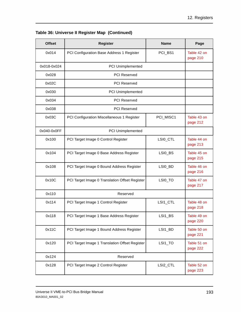
12. Registers
0x014 PCI Configuration Base Address 1 Register PCI_BS1 Table 42 on page 210
0x018-0x024 PCI Unimplemented
0x028 PCI Reserved
0x02C PCI Reserved
0x030 PCI Unimplemented
0x034 PCI Reserved
0x038 PCI Reserved
0x03C PCI Configuration Miscellaneous 1 Register PCI_MISC1 Table 43 on page 212
0x040-0x0FF PCI Unimplemented
0x100 PCI Target Image 0 Control Register LSI0_CTL Table 44 on page 213
0x104 PCI Target Image 0 Base Address Register LSI0_BS Table 45 on page 215
0x108 PCI Target Image 0 Bound Address Register LSI0_BD Table 46 on page 216
0x10C PCI Target Image 0 Translation Offset Register LSI0_TO Table 47 on page 217
0x110 Reserved
0x114 PCI Target Image 1 Control Register LSI1_CTL Table 48 on page 218
0x118 PCI Target Image 1 Base Address Register LSI1_BS Table 49 on page 220
0x11C PCI Target Image 1 Bound Address Register LSI1_BD Table 50 on page 221
0x120 PCI Target Image 1 Translation Offset Register LSI1_TO Table 51 on page 222
0x124 Reserved
0x128 PCI Target Image 2 Control Register LSI2_CTL Table 52 on page 223
Table 36: Universe II Register Map (Continued)
Offset Register Name Page
Universe II VME-to-PCI Bus Bridge Manual 19380A3010_MA001_02

12. Registers
0x12C PCI Target Image 2 Base Address Register LSI2_BS Table 53 on page 225
0x130 PCI Target Image 2 Bound Address Register LSI2_BD Table 54 on page 226
0x134 PCI Target Image 2 Translation Offset Register LSI2_TO Table 55 on page 227
0x138 Reserved
0x13C PCI Target Image 3 Control Register LSI3_CTL Table 56 on page 228
0x140 PCI Target Image 3 Base Address Register LSI3_BS Table 57 on page 230
0x144 PCI Target Image 3 Bound Address Register LSI3_BD Table 58 on page 231
0x148 PCI Target Image 3 Translation Offset Register LSI3_TO Table 59 on page 232
0x14C-0x16C Reserved
0x170 Special Cycle Control Register SCYC_CTL Table 60 on page 233
0x174 Special Cycle PCI Bus Address Register SCYC_ADDR Table 61 on page 234
0x178 Special Cycle Swap/Compare Enable Register SCYC_EN Table 62 on page 235
0x17C Special Cycle Compare Data Register SCYC_CMP Table 63 on page 236
0x180 Special Cycle Swap Data Register SCYC_SWP Table 64 on page 237
0x184 PCI Miscellaneous Register LMISC Table 65 on page 238
0x188 Special PCI Target Image Register SLSI Table 66 on page 239
0x18C PCI Command Error Log Register L_CMDERR Table 67 on page 241
Table 36: Universe II Register Map (Continued)
Offset Register Name Page
Universe II VME-to-PCI Bus Bridge Manual19480A3010_MA001_02

12. Registers
0x190 PCI Address Error Log Register LAERR Table 68 on page 242
0x194-0x19C Reserved
0x1A0 PCI Target Image 4 Control Register LSI4_CTL Table 69 on page 243
0x1A4 PCI Target Image 4 Base Address Register LSI4_BS Table 70 on page 245
0x1A8 PCI Target Image 4 Bound Address Register LSI4_BD Table 71 on page 246
0x1AC PCI Target Image 4 Translation Offset Register LSI4_TO Table 72 on page 247
0x1B0 Reserved
0x1B4 PCI Target Image 5 Control Register LSI5_CTL Table 73 on page 248
0x1B8 PCI Target Image 5 Base Address Register LSI5_BS Table 74 on page 250
0x1BC PCI Target Image 5 Bound Address Register LSI5_BD Table 75 on page 251
0x1C0 PCI Slave Image 5 Translation Offset Register LSI5_TO Table 76 on page 252
0x1C4 Reserved
0x1C8 PCI Target Image 6 Control Register LSI6_CTL Table 77 on page 253
0x1CC PCI Target Image 6 Base Address Register LSI6_BS Table 78 on page 255
0x1D0 PCI Target Image 6 Bound Address Register LSI6_BD Table 79 on page 256
0x1D4 PCI Target Image 6 Translation Offset Register LSI6_TO Table 80 on page 257
0x1D8 Reserved
0x1DC PCI Target Image 7 Control Register LSI7_CTL Table 81 on page 258
Table 36: Universe II Register Map (Continued)
Offset Register Name Page
Universe II VME-to-PCI Bus Bridge Manual 19580A3010_MA001_02

12. Registers
0x1E0 PCI Target Image 7 Base Address Register LSI7_BS Table 82 on page 260
0x1E4 PCI Target Image 7 Bound Address Register LSI7_BD Table 83 on page 261
0x1E8 PCI Target Image 7 Translation Offset Register LSI7_TO Table 84 on page 262
0x1EC-0x1FC Reserved
0x200 DMA Transfer Control Register DCTL Table 85 on page 263
0x204 DMA Transfer Byte Count Register DTBC Table 86 on page 265
0x208 DMA PCI Bus Address Register DLA Table 87 on page 266
0x20C Reserved
0x210 DMA VMEbus Address Register DVA Table 88 on page 267
0x214 Reserved
0x218 DMA Command Packet Pointer Register DCPP Table 89 on page 268
0x21C Reserved
0x220 DMA General Control and Status Register DGCS Table 90 on page 269
0x224 DMA Linked List Update Enable Register D_LLUE Table 91 on page 273
0x2280x-2FC Reserved
0x300 PCI Interrupt Enable Register LINT_EN Table 92 on page 274
0x304 PCI Interrupt Status Register LINT_STAT Table 93 on page 277
0x308 PCI Interrupt Map 0 Register LINT_MAP0 Table 94 on page 280
Table 36: Universe II Register Map (Continued)
Offset Register Name Page
Universe II VME-to-PCI Bus Bridge Manual19680A3010_MA001_02

12. Registers
0x30C PCI Interrupt Map 1 Register LINT_MAP1 Table 95 on page 281
0x310 VMEbus Interrupt Enable Register VINT_EN Table 96 on page 282
0x314 VMEbus Interrupt Status Register VINT_STAT Table 97 on page 285
0x318 VMEbus Interrupt Map 0 Register VINT_MAP0 Table 98 on page 287
0x31C VMEbus Interrupt Map 1 Register VINT_MAP1 Table 99 on page 288
0x320 Interrupt Status/ID Out Register STATID Table 100 on page 289
0x324 VIRQ1 STATUS/ID Register V1_STATID Table 101 on page 290
0x328 VIRQ2 STATUS/ID Register V2_STATID Table 102 on page 291
0x32C VIRQ3 STATUS/ID Register V3_STATID Table 103 on page 292
0x330 VIRQ4 STATUS/ID Register V4_STATID Table 104 on page 293
0x334 VIRQ5 STATUS/ID Register V5_STATID Table 105 on page 294
0x338 VIRQ6 STATUS/ID Register V6_STATID Table 106 on page 295
0x33C VIRQ7 STATUS/ID Register V7_STATID Table 107 on page 296
0x340 PCI Interrupt Map 2 Register LINT_MAP2 Table 108 on page 297
0x344 VME Interrupt Map 1 Register VINT_MAP2 Table 109 on page 298
0x348 Mailbox 0 Register MBOX0 Table 110 on page 299
Table 36: Universe II Register Map (Continued)
Offset Register Name Page
Universe II VME-to-PCI Bus Bridge Manual 19780A3010_MA001_02

12. Registers
0x34C Mailbox 1 Register MBOX1 Table 111 on page 300
0x350 Mailbox 2 Register MBOX2 Table 112 on page 301
0x354 Mailbox 3 Register MBOX3 Table 113 on page 302
0x358 Semaphore 0 Register SEMA0 Table 114 on page 303
0x35C Semaphore 1 Register SEMA1 Table 115 on page 304
0x360-0x3FC Reserved
0x400 Master Control Register MAST_CTL Table 116 on page 305
0x404 Miscellaneous Control Register MISC_CTL Table 117 on page 308
0x408 Miscellaneous Status Register MISC_STAT Table 118 on page 311
0x40C User AM Codes Register USER_AM Table 119 on page 313
0x410-0x4F8 Reserved
0x4FC Universe II Specific Register U2SPEC Table 120 on page 314
0x500-0xEFC Reserved
0xF00 VMEbus Slave Image 0 Control Register VSI0_CTL Table 121 on page 316
0xF04 VMEbus Slave Image 0 Base Address Register VSI0_BS Table 122 on page 318
0xF08 VMEbus Slave Image 0 Bound Address Register
VSI0_BD Table 123 on page 319
0xF0C VMEbus Slave Image 0 Translation Offset Register
VSI0_TO Table 124 on page 320
0xF10 Reserved
Table 36: Universe II Register Map (Continued)
Offset Register Name Page
Universe II VME-to-PCI Bus Bridge Manual19880A3010_MA001_02

12. Registers
0xF14 VMEbus Slave Image 1 Control Register VSI1_CTL Table 125 on page 321
0xF18 VMEbus Slave Image 1 Base Address Register VSI1_BS Table 126 on page 323
0xF1C VMEbus Slave Image 1 Bound Address Register
VSI1_BD Table 127 on page 324
0xF20 VMEbus Slave Image 1 Translation Offset Register
VSI1_TO Table 128 on page 325
0xF24 Reserved
0xF28 VMEbus Slave Image 2 Control Register VSI2_CTL Table 129 on page 326
0xF2C VMEbus Slave Image 2 Base Address Register VSI2_BS Table 130 on page 328
0xF30 VMEbus Slave Image 2 Bound Address Register
VSI2_BD Table 131 on page 329
0xF34 VMEbus Slave Image 2 Translation Offset Register
VSI2_TO Table 132 on page 330
0xF38 Reserved
0xF3C VMEbus Slave Image 3 Control Register VSI3_CTL Table 133 on page 331
0xF40 VMEbus Slave Image 3 Base Address Register VSI3_BS Table 134 on page 333
0xF44 VMEbus Slave Image 3 Bound Address Register
VSI3_BD Table 135 on page 334
0xF48 VMEbus Slave Image 3 Translation Offset Register
VSI3_TO Table 136 on page 335
0xF4C-0xF60 Reserved
0xF64 Location Monitor Control Register LM_CTL Table 137 on page 336
0xF68 Location Monitor Base Address Register LM_BS Table 138 on page 338
0xF6C Reserved
Table 36: Universe II Register Map (Continued)
Offset Register Name Page
Universe II VME-to-PCI Bus Bridge Manual 19980A3010_MA001_02

12. Registers
0xF70 VMEbus Register Access Image Control Register
VRAI_CTL Table 139 on page 339
0xF74 VMEbus Register Access Image Base Address Register
VRAI_BS Table 140 on page 340
0xF78-0xF7C Reserved
0xF80 VMEbus CSR Control Register VCSR_CTL Table 142 on page 341
0xF84 VMEbus CSR Translation Offset Register VCSR_TO Table 143 on page 342
0xF88 VMEbus AM Code Error Log Register V_AMERR Table 144 on page 343
0xF8C VMEbus Address Error Log Register VAERR Table 145 on page 344
0xF90 VMEbus Slave Image 4 Control Register VSI4_CTL Table 146 on page 345
0xF94 VMEbus Slave Image 4 Base Address Register VSI4_BS Table 147 on page 347
0xF98 VMEbus Slave Image 4 Bound Address Register
VSI4_BD Table 148 on page 348
0xF9C VMEbus Slave Image 4 Translation Offset Register
VSI4_TO Table 149 on page 349
0xFA0 Reserved
0xFA4 VMEbus Slave Image 5 Control Register VSI5_CTL Table 150 on page 350
0xFA8 VMEbus Slave Image 5 Base Address Register VSI5_BS Table 151 on page 352
0xFAC VMEbus Slave Image 5 Bound Address Register
VSI5_BD Table 152 on page 353
0xFB0 VMEbus Slave Image 5 Translation Offset Register
VSI5_TO Table 153 on page 354
0xFB4 Reserved
0xFB8 VMEbus Slave Image 6 Control Register VSI6_CTL Table 154 on page 355
Table 36: Universe II Register Map (Continued)
Offset Register Name Page
Universe II VME-to-PCI Bus Bridge Manual20080A3010_MA001_02

12. Registers
0xFBC VMEbus Slave Image 6 Base Address Register VSI6_BS Table 155 on page 357
0xFC0 VMEbus Slave Image 6 Bound Address Register
VSI6_BD Table 156 on page 358
0xFC4 VMEbus Slave Image 6 Translation Offset Register
VSI6_TO Table 157 on page 359
0xFC8 Reserved
0xFCC VMEbus Slave Image 7 Control Register VSI7_CTL Table 158 on page 360
0xFD0 VMEbus Slave Image 7 Base Address Register VSI7_BS Table 159 on page 362
0xFD4 VMEbus Slave Image 7 Bound Address Register
VSI7_BD Table 160 on page 363
0xFD8 VMEbus Slave Image 7 Translation Offset Register
VSI7_TO Table 161 on page 364
0xFDC-0xFEC Reserved
0xFF0 VME CR/CSR Reserved
0xFF4 VMEbus CSR Bit Clear Register VCSR_CLR Table 162 on page 365
0xFF8 VMEbus CSR Bit Set Register VCSR_SET Table 163 on page 366
0xFFC VMEbus CSR Base Address Register VCSR_BS Table 164 on page 367
Table 36: Universe II Register Map (Continued)
Offset Register Name Page
Universe II VME-to-PCI Bus Bridge Manual 20180A3010_MA001_02

12. Registers
12.2.1 PCI Configuration Space ID Register (PCI_ID) Table 37: PCI Configuration Space ID Register (PCI_ID)
Register Name: PCI_ID Register Offset: 0x000
Bits Function
31-24 DID
23-16 DID
15-08 VID
07-00 VID
PCI_ID Description
Name Type Reset ByReset State Function
DID[15:0] R all 0 Device ID - Tundra allocated device identifier
VID[15:0] R all 10E3 Vendor ID - PCI SIG allocated vendor identifier
Universe II VME-to-PCI Bus Bridge Manual20280A3010_MA001_02

12. Registers
12.2.2 PCI Configuration Space Control and Status Register (PCI_CSR)
Table 38: PCI Configuration Space Control and Status Register (PCI_CSR)
Register Name: PCI_CSR Register Offset: 0x004
Bits Function
31-24 D_PE S_SERR R_MA R_TA S_TA DEVSEL DP_D
23-16 TFBBC PCI Reserved
15-08 PCI Reserved MFBBC SERR_EN
07-00 WAIT PERESP VGAPS MWI_EN SC BM MS IOS
PCI_CSR Description
Name Type Reset By Reset State Function
D_PE R/Write 1 to
Clear
all 0 Detected Parity Error
0=No parity error
1=Parity error
This bit is always set by the Universe II when the PCI master interface detects a data parity error or the PCI target interface detects address or data parity errors.
S_SERR R/Write 1 to
Clear
all 0 Signalled SERR_
0=SERR_ not asserted
1=SERR_ asserted.
The Universe II PCI target interface sets this bit when it asserts SERR_ to signal an address parity error. SERR_EN must be set before SERR_ can be asserted.
R_MA R/Write 1 to
Clear
all 0 Received Master-Abort
0=Master did not generate Master-Abort
1=Master generated Master-Abort
The Universe II PCI master interface sets this bit when a transaction it initiated had to be terminated with a Master-Abort.
Universe II VME-to-PCI Bus Bridge Manual 20380A3010_MA001_02

12. Registers
R_TA R/Write 1 to
Clear
all 0 Received Target-Abort
0=Master did not detect Target-Abort
1=Master detected Target-Abort.
The Universe II PCI master interface sets this bit when a transaction it initiated was terminated with a Target-Abort.
S_TA R/Write 1 to
Clear
all 0 Signalled Target-Abort
0=Target did not terminate transaction with Target-Abort
1=Target terminated transaction with Target-Abort.
DEVSEL R all 01 Device Select Timing
The Universe II is a medium speed device
DP_D R/Write 1 to
Clear
all 0 Master Data Parity Error
0=Master did not detect/generate data parity error, 1=Master detected/generated data parity error.
The Universe II PCI master interface sets this bit if the Parity Error Response bit is set, if it is the master of transaction in which it asserts PERR_, or the addressed target asserts PERR_.
TFBBC R all 0 Target Fast Back to Back Capable
Universe II cannot accept Back to Back cycles from a different agent.
MFBBC R all 0 Master Fast Back to Back Enable
0=no fast back-to-back transactions
The Universe II master never generates fast back to back transactions.
SERR_EN R/W all 0 SERR_ Enable
0=Disable SERR_ driver
1=Enable SERR_ driver.
Setting this and PERESP allows the Universe II PCI target interface to report address parity errors with SERR_.
PCI_CSR Description
Name Type Reset By Reset State Function
Universe II VME-to-PCI Bus Bridge Manual20480A3010_MA001_02

12. Registers
WAIT R all 0 Wait Cycle Control
0=No address/data stepping
PERESP R/W all 0 Parity Error Response
0=Disable
1=Enable
Controls the Universe II response to data and address parity errors. When enabled, it allows the assertion of PERR_ to report data parity errors. When this bit and SERR_EN are asserted, the Universe II can report address parity errors on SERR_. Universe II parity generation is unaffected by this bit.
VGAPS R all 0 VGA Palette Snoop
0=Disable
The Universe II treats palette accesses like all other accesses.
MWI_EN R all 0 Memory Write and Invalidate Enable
0=Disable
The Universe II PCI master interface never generates a Memory Write and Invalidate command.
SC R all 0 Special Cycles
0=Disable
The Universe II PCI target interface never responds to special cycles.
BM R/W PWR VME This bit is 1 after reset if the VMEbus Address [14] equals 1 during power-on reset.
This bit is reloaded by “all”.
Master Enable
0=Disable
1=Enable
For a VMEbus slave image to respond to an incoming cycle, this bit must be set. If this bit is cleared while there is data in the VMEbus Slave Posted Write FIFO, the data will be written to the PCI bus but no further data will be accepted into this FIFO until the bit is set.
PCI_CSR Description
Name Type Reset By Reset State Function
Universe II VME-to-PCI Bus Bridge Manual 20580A3010_MA001_02

12. Registers
The Universe II only refuses PCI addresses with parity errors when both the PERESP and SERR_EN bits are programmed to a value of 1.
MS R/W PWR VME This bit is 1 after reset if the VMEbus Address [13:12] equals 10 during power-on reset. This bit is reloaded by “all”
Target Memory Enable
0=Disable
1=Enable
IOS R/W PWR VME This bit is 1 after reset if the VMEbus Address [13:12] equals 10 during power-on reset. This bit is reloaded by “all”
Target IO Enable
0=Disable
1=Enable
PCI_CSR Description
Name Type Reset By Reset State Function
Universe II VME-to-PCI Bus Bridge Manual20680A3010_MA001_02

12. Registers
12.2.3 PCI Configuration Class Register (PCI_CLASS)Table 39: PCI Configuration Class Register (PCI_CLASS)
Register Name: PCI_CLASS Register Offset: 0x008
Bits Function
31-24 BASE
23-16 SUB
15-08 PROG
07-00 RID
PCI_CLASS Description
Name Type Reset ByReset State Function
BASE [7:0] R all 06 Base Class Code
The Universe II is defined as a PCI bridge device
SUB [7:0] R all 80 Sub Class Code
The Universe II sub-class is “other bridge device”
PROG [7:0] R all 00 Programming Interface
The Universe II does not have a standardized register-level programming interface
RID [7:0] R all 02 Revision ID
Universe II VME-to-PCI Bus Bridge Manual 20780A3010_MA001_02

12. Registers
12.2.4 PCI Configuration Miscellaneous 0 Register (PCI_MISC0)The Universe II is not a multi-function device.
LTIMER: When the Universe II latency timer is programmed for eight clock periods and FRAME_, IRDY_ and TRDY_ are asserted while GNT_ is not asserted, FRAME_ is negated on the next clock edge.
Table 40: PCI Configuration Miscellaneous 0 Register (PCI_MISC0)
Register Name: PCI_MISC0 Register Offset: 0x00C
Bits Function
31-24 BISTC SBIST PCI Reserved CCODE
23-16 MFUNCT LAYOUT
15-08 LTIMER 0 0 0
07-00 PCI Unimplemented
PCI_MISC0 Description
Name Type Reset ByReset State Function
BISTC R all 0 The Universe II is not BIST Capable
SBIST R all 0 Start BIST
The Universe II is not BIST capable
CCODE R all 0 Completion Code
The Universe II is not BIST capable
MFUNCT R all 0 Multifunction Device
0=No
1=Yes
The Universe II is not a multi-function device.
LAYOUT R all 0 Configuration Space Layout
LTIMER [7:3] R/W all 0 Latency Timer: The latency timer has a resolution of eight clocks
Universe II VME-to-PCI Bus Bridge Manual20880A3010_MA001_02

12. Registers
12.2.5 PCI Configuration Base Address Register (PCI_BS0)This register specifies the 4 Kbyte aligned base address of the 4 Kbyte Universe II register space on PCI.
A power-up option determines if the registers are mapped into Memory or I/O space in relation to this base address. (See “Power-Up Options” on page 160). If mapped into Memory space, the user is free to locate the registers anywhere in the 32-bit address space. If PCI_BS0 is mapped to Memory space, PCI_BS1 is mapped to I/O space; if PCI_BS0 is mapped to I/O space, then PCI_BS1 is mapped to Memory space.
• When the VA[1] pin is sampled low at power-up, the PCI_BS0 register’s SPACE bit is set to 1, which signifies I/O space, and the PCI_BS1 register’s SPACE bit is set to 0, which signifies memory space.
• When VA[1] is sampled high at power-up, the PCI_BS0 register’s SPACE register’s bit is set to 0, which signifies Memory space, and the PCI_BS1 register’s SPACE bit is set to 1, which signifies I/O space.
A write must occur to this register before the Universe II Device Specific Registers can be accessed. This write can be performed with a PCI configuration transaction or a VMEbus register access.
Table 41: PCI Configuration Base Address Register (PCI_BS0)
Register Name: PCI_BS0 Register Offset: 0x010
Bits Function
31-24 BS
23-16 BS
15-08 BS 0 0 0 0
07-00 0 0 0 0 0 0 0 SPACE
PCI_BS0 Description
Name Type Reset ByReset State Function
BS[31:12] R/W all 0 Base Address
SPACE R all Power-up Option
PCI Bus Address Space
0=Memory
1=I/O
Universe II VME-to-PCI Bus Bridge Manual 20980A3010_MA001_02

12. Registers
12.2.6 PCI Configuration Base Address 1 Register (PCI_BS1)This register specifies the 4 KByte aligned base address of the 4 KByte Universe II register space in PCI.
A power-up option determines the value of the SPACE bit. This determines whether the registers are mapped into Memory or I/O space in relation to this base address. (See “Power-Up Options” on page 160). If mapped into Memory space, the user is free to locate the Universe registers anywhere in the 32-bit address space. If PCI_BS0 is mapped to Memory space, PCI_BS1 is mapped to I/O space; if PCI_BS0 is mapped to I/O space, then PCI_BS1 is mapped to Memory space.
• When the VA[1] pin is sampled low at power-up, the PCI_BS0 register’s SPACE bit is set to “1”, which signifies I/O space, and the PCI_BS1 register’s SPACE bit is set to “0”, which signifies memory space.
• When VA[1] is sampled high at power-up, the PCI_BS0 register’s SPACE register’s bit is set to “0”, which signifies Memory space, and the PCI_BS1 register’s SPACE bit is set to “1”, which signifies I/O space.
A write must occur to this register before the Universe II Device Specific Registers can be accessed. This write can be performed with a PCI configuration transaction or a VMEbus register access.
Table 42: PCI Configuration Base Address 1 Register (PCI_BS1)
Register Name: PCI_BS1 Register Offset: 0x014
Bits Function
31-24 BS
23-16 BS
15-08 BS 0 0 0 0
07-00 0 0 0 0 0 0 0 SPACE
PCI_BS1 Description
Name Type Reset ByReset State Function
BS[31:12] R/W all 0 Base Address
SPACE R all Power-up Option
PCI Bus Address Space
0=Memory
1=I/O
Universe II VME-to-PCI Bus Bridge Manual21080A3010_MA001_02

12. Registers
The SPACE bit in this register is an inversion of the SPACE field in PCI_BS0.
Universe II VME-to-PCI Bus Bridge Manual 21180A3010_MA001_02

12. Registers
12.2.7 PCI Configuration Miscellaneous 1 Register (PCI_MISC1)
The MIN_GNT parameter assumes the Universe II master is transferring an aligned burst size of 64 bytes to a 32-bit target with no wait states. This would require roughly 20 clocks (at a clock frequency of 33 MHz, this is about 600 ns). MIN_GNT is set to three, or 750 ns.
Table 43: PCI Configuration Miscellaneous 1 Register (PCI_MISC1)
Register Name: PCI_MISC1 Register Offset: 0x03C
Bits Function
31-24 MAX_LAT [7:0
23-16 MIN_GNT [7:0
15-08 INT_PIN [7:0
07-00 INT_LINE [7:0
PCI_MISC1 Description
Name Type Reset ByReset State Function
MAX_LAT[7:0] R all 0 Maximum Latency: This device has no special latency requirements
MIN_GNT[7:0] R all 00000011 Minimum Grant: 250 ns
INT_PIN[7:0] R all 00000001 Interrupt Pin: Universe II pin INT_ [0] has a PCI compliant I/O buffer
INT_LINE[7:0] R/W all 0 Interrupt Line: used by some PCI systems to record interrupt routing information
Universe II VME-to-PCI Bus Bridge Manual21280A3010_MA001_02

12. Registers
12.2.8 PCI Target Image 0 Control (LSI0_CTL)Table 44: PCI Target Image 0 Control (LSI0_CTL)
Register Name: LSI0_CTL Register Offset: 0x100
Bits Function
31-24 EN PWEN Reserved
23-16 VDW Reserved VAS
15-08 Reserved PGM Reserved SUPER Reserved VCT
07-00 Reserved LAS
LSI0_CTL Description
Name Type Reset ByReset State Function
EN R/W all Power-up Option
Image Enable
0=Disable
1=Enable
PWEN R/W all 0 Posted Write Enable
0=Disable
1=Enable
VDW R/W all 10 VMEbus Maximum Datawidth
00=8-bit data width
01=16 bit data width
10=32-bit data width
11=64-bit data width
VAS R/W all Power-up Option
VMEbus Address Space
000=A16
001=A24
010=A32
011= Reserved
100=Reserved
101=CR/CSR
110=User1
111=User2
Universe II VME-to-PCI Bus Bridge Manual 21380A3010_MA001_02

12. Registers
In the PCI Target Image Control register, setting the VCT bit will only have effect if the VAS bits are programmed for A24 or A32 space and the VDW bits are programmed for 8-bit, 16-bit, or 32-bit.
If VAS bits are programmed to A24 or A32 and the VDW bits are programmed for 64-bit, the Universe II may perform MBLT transfers independent of the state of the VCT bit.
The setting of the PWEN bit is ignored if the LAS bit is programmed for PCI Bus I/O Space, forcing all transactions through this image to be coupled.
PGM R/W all 0 Program/Data AM Code
0=Data
1=Program
SUPER R/W all 0 Supervisor/User AM Code
0=Non-Privileged
1=Supervisor
VCT R/W all 0 VMEbus Cycle Type
0=No BLTs on VMEbus
1=Single BLTs on VMEbus
LAS R/W all Power-up Option
PCI Bus Memory Space
0=PCI Bus Memory Space
1=PCI Bus I/O Space
LSI0_CTL Description
Name Type Reset ByReset State Function
Universe II VME-to-PCI Bus Bridge Manual21480A3010_MA001_02

12. Registers
12.2.9 PCI Target Image 0 Base Address Register (LSI0_BS)The base address specifies the lowest address in the address range that will be decoded.
The base address for PCI Target Image 0 and PCI Target Image 4 have a 4 Kbyte resolution. PCI Target Images 1, 2, 3, 5, 6, and 7 have a 64 Kbyte resolution.
Table 45: PCI Target Image 0 Base Address Register (LSI0_BS)
Register Name: LSI0_BS Register Offset: 0x104
Bits Function
31-24 BS
23-16 BS
15-08 BS Reserved
07-00 Reserved
LSI0_BS Description
Name Type Reset ByReset State Function
BS[31:28] R/W all Power-up Option
Base Address
BS[27:12] R/W all 0 Base Address
Universe II VME-to-PCI Bus Bridge Manual 21580A3010_MA001_02

12. Registers
12.2.10 PCI Target Image 0 Bound Address Register (LSI0_BD)
The addresses decoded in a slave image are those which are greater than or equal to the base address and less than the bound register. If the bound address is 0, then the addresses decoded are those greater than or equal to the base address.
The bound address for PCI Target Image 0 and PCI Target Image 4 have a 4Kbyte resolution. PCI Target Images 1, 2, 3, 5, 6, and 7 have a 64Kbyte resolution.
Table 46: PCI Target Image 0 Bound Address Register (LSI0_BD)
Register Name: LSI0_BD Register Offset: 0x108
Bits Function
31-24 BD
23-16 BD
15-08 BD Reserved
07-00 Reserved
LSI0_BD Description
Name Type Reset ByReset State Function
BD[31:28] R/W all Power-up Option
Bound Address
BD[27:12] R/W all 0 Bound Address
Universe II VME-to-PCI Bus Bridge Manual21680A3010_MA001_02

12. Registers
12.2.11 PCI Target Image 0 Translation Offset (LSI0_TO)The translation offset for PCI Target Image 0 and PCI Target Image 4 have a 4Kbyte resolution. PCI Target Images 1, 2, 3, 5, 6, and 7 have a 64Kbyte resolution.
Address bits [31:12] generated on the VMEbus in response to an image decode are a two’s complement addition of address bits [31:12] on the PCI Bus and bits [31:12] of the image’s translation offset.
Table 47: PCI Target Image 0 Translation Offset (LSI0_TO)
Register Name: LSI0_TO Register Offset: 0x10C
Bits Function
31-24 TO
23-16 TO
15-08 TO Reserved
07-00 Reserved
LSI0_TO Description
Name Type Reset ByReset State Function
TO[31:12] R/W all 0 Translation Offset
Universe II VME-to-PCI Bus Bridge Manual 21780A3010_MA001_02

12. Registers
12.2.12 PCI Target Image 1 Control (LSI1_CTL) Table 48: PCI Target Image 1 Control (LSI1_CTL)
Register Name: LSI1_CTL Register Offset: 0x114
Bits Function
31-24 EN PWEN Reserved
23-16 VDW Reserved VAS
15-08 Reserved PGM Reserved SUPER Reserved VCT
07-00 Reserved LAS
LSI1_CTL Description
Name Type Reset ByReset State Function
EN R/W all 0 Image Enable
0=Disable
1=Enable
PWEN R/W all 0 Posted Write Enable
0=Disable
1=Enable
VDW R/W all 10 VMEbus Maximum Datawidth
00=8-bit data width
01=16 bit data width
10=32-bit data width
11=64-bit data width
VAS R/W all 0 VMEbus Address Space
000=A16
001=A24
010=A32
011= Reserved
100=Reserved
101=CR/CSR
110=User1
111=User2
Universe II VME-to-PCI Bus Bridge Manual21880A3010_MA001_02

12. Registers
In the PCI Target Image Control register, setting the VCT bit will only have effect if the VAS bits are programmed for A24 or A32 space and the VDW bits are programmed for 8-bit, 16-bit, or 32-bit.
If VAS bits are programmed to A24 or A32 and the VDW bits are programmed for 64-bit, the Universe II may perform MBLT transfers independent of the state of the VCT bit.
The setting of the PWEN bit is ignored if the LAS bit is programmed for PCI Bus I/O Space, forcing all transactions through this image to be coupled.
PGM R/W all 0 Program/Data AM Code
0=Data
1=Program
SUPER R/W all 0 Supervisor/User AM Code
0=Non-Privileged
1=Supervisor
VCT R/W all 0 VMEbus Cycle Type
0=no BLTs on VMEbus
1=BLTs on VMEbus
LAS R/W all 0 PCI Bus Memory Space
0=PCI Bus Memory Space
1=PCI Bus I/O Space
LSI1_CTL Description
Name Type Reset ByReset State Function
Universe II VME-to-PCI Bus Bridge Manual 21980A3010_MA001_02

12. Registers
12.2.13 PCI Target Image 1 Base Address Register (LSI1_BS)The base address specifies the lowest address in the address range that will be decoded.
Table 49: PCI Target Image 1 Base Address Register (LSI1_BS)
Register Name: LSI1_BS Register Offset: 0x118
Bits Function
31-24 BS
23-16 BS
15-08 Reserved
07-00 Reserved
LSI1_BS Description
Name Type Reset ByReset State Function
BS[31:16] R/W all 0 Base Address
Universe II VME-to-PCI Bus Bridge Manual22080A3010_MA001_02

12. Registers
12.2.14 PCI Target Image 1 Bound Address Register (LSI1_BD)The addresses decoded in a slave image are those which are greater than or equal to the base address and less than the bound register. If the bound address is 0, then the addresses decoded are those greater than or equal to the base address.
The bound address for PCI Target Image 0 and PCI Target Image 4 have a 4Kbyte resolution. PCI Target Images 1, 2, 3, 5, 6, and 7 have a 64Kbyte resolution.
Table 50: PCI Target Image 1 Bound Address Register (LSI1_BD)
Register Name: LSI1_BD Register Offset: 0x11C
Bits Function
31-24 BD
23-16 BD
15-08 Reserved
07-00 Reserved
LSI1_BD Description
Name Type Reset ByReset State Function
BD[31:16] R/W all 0 Bound Address
Universe II VME-to-PCI Bus Bridge Manual 22180A3010_MA001_02

12. Registers
12.2.15 PCI Target Image 1 Translation Offset (LSI1_TO)
Address bits [31:16] generated on the VMEbus in response to an image decode are a two’s complement addition of address bits [31:16] on the PCI Bus and bits [31:16] of the image’s translation offset.
Table 51: PCI Target Image 1 Translation Offset (LSI1_TO)
Register Name: LSI1_TO Register Offset: 0x120
Bits Function
31-24 TO
23-16 TO
15-08 Reserved
07-00 Reserved
LSI1_TO Description
Name Type Reset ByReset State Function
TO[31:16] R/W all 0 Translation offset
Universe II VME-to-PCI Bus Bridge Manual22280A3010_MA001_02

12. Registers
12.2.16 PCI Target Image 2 Control (LSI2_CTL) Table 52: PCI Target Image 2 Control (LSI2_CTL)
Register Name: LSI2_CTL Register Offset: 0x128
Bits Function
31-24 EN PWEN Reserved
23-16 VDW Reserved VAS
15-08 Reserved PGM Reserved SUPER Reserved VCT
07-00 Reserved LAS
LSI2_CTL Description
Name Type Reset ByReset State Function
EN R/W all 0 Image Enable
0=Disable
1=Enable
PWEN R/W all 0 Posted Write Enable
0=Disable
1=Enable
VDW R/W all 10 VMEbus Maximum Datawidth
00=8-bit data width
01=16 bit data width
10=32-bit data width
11=64-bit data width
VAS R/W all 0 VMEbus Address Space
000=A16
001=A24
010=A32
011= Reserved
100=Reserved
101=CR/CSR
110=User1
111=User2
Universe II VME-to-PCI Bus Bridge Manual 22380A3010_MA001_02
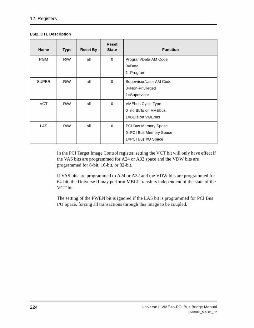
12. Registers
In the PCI Target Image Control register, setting the VCT bit will only have effect if the VAS bits are programmed for A24 or A32 space and the VDW bits are programmed for 8-bit, 16-bit, or 32-bit.
If VAS bits are programmed to A24 or A32 and the VDW bits are programmed for 64-bit, the Universe II may perform MBLT transfers independent of the state of the VCT bit.
The setting of the PWEN bit is ignored if the LAS bit is programmed for PCI Bus I/O Space, forcing all transactions through this image to be coupled.
PGM R/W all 0 Program/Data AM Code
0=Data
1=Program
SUPER R/W all 0 Supervisor/User AM Code
0=Non-Privileged
1=Supervisor
VCT R/W all 0 VMEbus Cycle Type
0=no BLTs on VMEbus
1=BLTs on VMEbus
LAS R/W all 0 PCI Bus Memory Space
0=PCI Bus Memory Space
1=PCI Bus I/O Space
LSI2_CTL Description
Name Type Reset ByReset State Function
Universe II VME-to-PCI Bus Bridge Manual22480A3010_MA001_02

12. Registers
12.2.17 PCI Target Image 2 Base Address Register (LSI2_BS)The base address specifies the lowest address in the address range that will be decoded.
Table 53: PCI Target Image 2 Base Address Register (LSI2_BS)
Register Name: LSI2_BS Register Offset: 0x12C
Bits Function
31-24 BS
23-16 BS
15-08 Reserved
07-00 Reserved
LSI2_BS Description
Name Type Reset ByReset State Function
BS[31:16] R/W all 0 Base Address
Universe II VME-to-PCI Bus Bridge Manual 22580A3010_MA001_02

12. Registers
12.2.18 PCI Target Image 2 Bound Address Register (LSI2_BD)The addresses decoded in a slave image are those which are greater than or equal to the base address and less than the bound register. If the bound address is 0, then the addresses decoded are those greater than or equal to the base address.
Table 54: PCI Target Image 2 Bound Address Register (LSI2_BD)
Register Name: LSI2_BD Register Offset: 0x130
Bits Function
31-24 BD
23-16 BD
15-08 Reserved
07-00 Reserved
LSI2_BD Description
Name Type Reset ByReset State Function
BD[31:16] R/W all 0 Bound Address
Universe II VME-to-PCI Bus Bridge Manual22680A3010_MA001_02

12. Registers
12.2.19 PCI Target Image 2 Translation Offset (LSI2_TO)
Address bits [31:16] generated on the VMEbus in response to an image decode are a two’s complement addition of address bits [31:16] on the PCI Bus and bits [31:16] of the image’s translation offset.
Table 55: PCI Target Image 2 Translation Offset (LSI2_TO)
Register Name: LSI2_TO Register Offset: 0x134
Bits Function
31-24 TO
23-16 TO
15-08 Reserved
07-00 Reserved
LSI2_TO Description
Name Type Reset ByReset State Function
TO[31:16] R/W all 0 Translation offset
Universe II VME-to-PCI Bus Bridge Manual 22780A3010_MA001_02
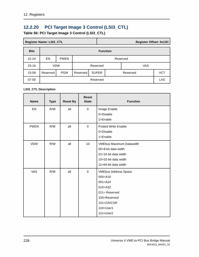
12. Registers
12.2.20 PCI Target Image 3 Control (LSI3_CTL) Table 56: PCI Target Image 3 Control (LSI3_CTL)
Register Name: LSI3_CTL Register Offset: 0x13C
Bits Function
31-24 EN PWEN Reserved
23-16 VDW Reserved VAS
15-08 Reserved PGM Reserved SUPER Reserved VCT
07-00 Reserved LAS
LSI3_CTL Description
Name Type Reset ByReset State Function
EN R/W all 0 Image Enable
0=Disable
1=Enable
PWEN R/W all 0 Posted Write Enable
0=Disable
1=Enable
VDW R/W all 10 VMEbus Maximum Datawidth
00=8-bit data width
01=16 bit data width
10=32-bit data width
11=64-bit data width
VAS R/W all 0 VMEbus Address Space
000=A16
001=A24
010=A32
011= Reserved
100=Reserved
101=CR/CSR
110=User1
111=User2
Universe II VME-to-PCI Bus Bridge Manual22880A3010_MA001_02

12. Registers
In the PCI Target Image Control register, setting the VCT bit will only have effect if the VAS bits are programmed for A24 or A32 space and the VDW bits are programmed for 8-bit, 16-bit, or 32-bit.
If VAS bits are programmed to A24 or A32 and the VDW bits are programmed for 64-bit, the Universe II may perform MBLT transfers independent of the state of the VCT bit.
The setting of the PWEN bit is ignored if the LAS bit is programmed for PCI Bus I/O Space, forcing all transactions through this image to be coupled.
PGM R/W all 0 Program/Data AM Code
0=Data
1=Program
SUPER R/W all 0 Supervisor/User AM Code
0=Non-Privileged
1=Supervisor
VCT R/W all 0 VMEbus Cycle Type
0=no BLTs on VMEbus
1=BLTs on VMEbus
LAS R/W all 0 PCI Bus Memory Space
0=PCI Bus Memory Space
1=PCI Bus I/O Space
LSI3_CTL Description
Name Type Reset ByReset State Function
Universe II VME-to-PCI Bus Bridge Manual 22980A3010_MA001_02

12. Registers
12.2.21 PCI Target Image 3 Base Address Register (LSI3_BS)The base address specifies the lowest address in the address range that will be decoded.
Table 57: PCI Target Image 3 Base Address Register (LSI3_BS)
Register Name: LSI3_BS Register Offset: 0x140
Bits Function
31-24 BS
23-16 BS
15-08 Reserved
07-00 Reserved
LSI3_BS Description
Name Type Reset ByReset State Function
BS[31:16] R/W all 0 Base Address
Universe II VME-to-PCI Bus Bridge Manual23080A3010_MA001_02

12. Registers
12.2.22 PCI Target Image 3 Bound Address Register (LSI3_BD)The addresses decoded in a slave image are those which are greater than or equal to the base address and less than the bound register. If the bound address is 0, then the addresses decoded are those greater than or equal to the base address.
Table 58: PCI Target Image 3 Bound Address Register (LSI3_BD)
Register Name: LSI3_BD Register Offset: 0x144
Bits Function
31-24 BD
23-16 BD
15-08 Reserved
07-00 Reserved
LSI3_BD Description
Name Type Reset ByReset State Function
BD[31:16] R/W all 0 Bound Address
Universe II VME-to-PCI Bus Bridge Manual 23180A3010_MA001_02

12. Registers
12.2.23 PCI Target Image 3 Translation Offset (LSI3_TO)
Address bits [31:16] generated on the VMEbus in response to an image decode are a two’s complement addition of address bits [31:16] on the PCI Bus and bits [31:16] of the image’s translation offset.
Table 59: PCI Target Image 3 Translation Offset (LSI3_TO)
Register Name: LSI3_TO Register Offset: 0x148
Bits Function
31-24 TO
23-16 TO
15-08 Reserved
07-00 Reserved
LSI3_TO Description
Name Type Reset ByReset State Function
TO[31:16] R/W all 0 Translation offset
Universe II VME-to-PCI Bus Bridge Manual23280A3010_MA001_02

12. Registers
12.2.24 Special Cycle Control Register (SCYC_CTL)The special cycle generator generates an ADOH or RMW cycle for the 32-bit PCI Bus address which matches the programmed address in SCYC_ADDR, in the address space specified in the LAS field of the SCYC_CTL register. A Read-Modify-Write command is initiated by a read to the specified address. Address-Only cycles are initiated by either read or write cycles.
Table 60: Special Cycle Control Register (SCYC_CTL)
Register Name: SCYC_CTL Register Offset: 0x170
Bits Function
31-24 Reserved
23-16 Reserved
15-08 Reserved
07-00 Reserved LAS SCYC
SCYC_CTL Description
Name Type Reset ByReset State Function
LAS R/W all 0 PCI Bus Address Space0=PCI Bus Memory Space
1=PCI Bus I/O Space
For a RMW cycle only.
SCYC R/W all 0 Special Cycle00=Disable
01=RMW
10=ADOH
11=Reserved
Universe II VME-to-PCI Bus Bridge Manual 23380A3010_MA001_02

12. Registers
12.2.25 Special Cycle PCI Bus Address Register (SCYC_ADDR)This register designates the special cycle address. This address must appear on the PCI Bus during the address phase of a transfer for the Special Cycle Generator to perform its function. Whenever the addresses match, the Universe II does not respond with ACK64_.
Table 61: Special Cycle PCI Bus Address Register (SCYC_ADDR)
Register Name: SCYC_ADDR Register Offset: 0x174
Bits Function
31-24 ADDR
23-16 ADDR
15-08 ADDR
07-00 ADDR Reserved
SCYC_ADDR Description
Name Type Reset ByReset State Function
ADDR
[31:2]
R/W all 0 Address
Universe II VME-to-PCI Bus Bridge Manual23480A3010_MA001_02

12. Registers
12.2.26 Special Cycle Swap/Compare Enable Register (SCYC_EN)The bits enabled in this register determine the bits that are involved in the compare and swap operations for VME RMW cycles.
Table 62: Special Cycle Swap/Compare Enable Register (SCYC_EN)
Register Name: SCYC_EN Register Offset: 0x178
Bits Function
31-24 EN
23-16 EN
15-08 EN
07-00 EN
SCYC_EN Description
Name Type Reset ByReset State Function
EN[31:0] R/W all 0 Bit Enable
0=Disable
1=Enable
Universe II VME-to-PCI Bus Bridge Manual 23580A3010_MA001_02

12. Registers
12.2.27 Special Cycle Compare Data Register (SCYC_CMP)The data returned from the read portion of a VMEbus RMW is compared with the contents of this register. SCYC_EN is used to control which bits are compared.
Table 63: Special Cycle Compare Data Register (SCYC_CMP)
Register Name: SCYC_CMP Register Offset: 0x17C
Bits Function
31-24 CMP
23-16 CMP
15-08 CMP
07-00 CMP
SCYC_CMP Description
Name Type Reset ByReset State Function
CMP[31:0] R/W all 0 The data returned from the VMEbus is compared with the contents of this register.
Universe II VME-to-PCI Bus Bridge Manual23680A3010_MA001_02
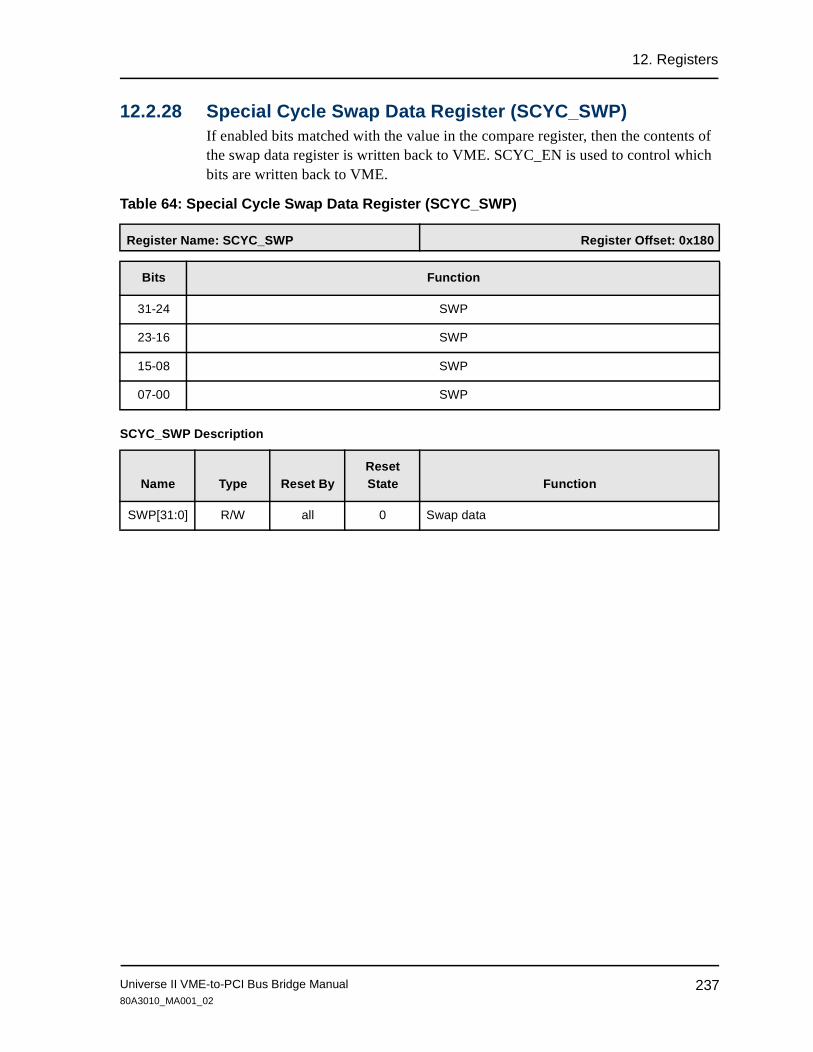
12. Registers
12.2.28 Special Cycle Swap Data Register (SCYC_SWP)If enabled bits matched with the value in the compare register, then the contents of the swap data register is written back to VME. SCYC_EN is used to control which bits are written back to VME.
Table 64: Special Cycle Swap Data Register (SCYC_SWP)
Register Name: SCYC_SWP Register Offset: 0x180
Bits Function
31-24 SWP
23-16 SWP
15-08 SWP
07-00 SWP
SCYC_SWP Description
Name Type Reset ByReset State Function
SWP[31:0] R/W all 0 Swap data
Universe II VME-to-PCI Bus Bridge Manual 23780A3010_MA001_02

12. Registers
12.2.29 PCI Miscellaneous Register (LMISC)This register can only be set at configuration or after disabling all PCI Target Images.
The Universe II uses CWT to determine how long to hold ownership of the VMEbus after processing a coupled transaction. The timer is restarted each time the Universe II processes a coupled transaction. If this timer expires, the PCI Slave Channel releases the VMEbus.
Table 65: PCI Miscellaneous Register (LMISC)
Register Name: LMISC Register Offset: 0x184
Bits Function
31-24 CRT[3:0] Reserved CWT
23-16 Reserved
15-08 Reserved
07-00 Reserved
SLSI Description
Name Type Reset ByReset State Function
CRT[3:0] R/W all 000 CRT
This field is provided for backward compatibility with the Universe I. It has no effect on the operation of the Universe II.
CWT [2:0] R/W all 000 Coupled Window Timer
000=Disable - release after first coupled transaction
001=16 PCI Clocks
010=32 PCI Clocks
011=64 PCI Clocks
100=128 PCI Clocks
101=256 PCI Clocks
110=512 PCI Clocks
others= Reserved
Device behavior is unpredictable if CWT is changed during coupled cycle activity.
Universe II VME-to-PCI Bus Bridge Manual23880A3010_MA001_02

12. Registers
12.2.30 Special PCI Target Image (SLSI)This register fully specifies an A32 capable special PCI Target Image. The base is programmable to a 64 Mbyte alignment, and the size is fixed at 64 Mbytes. Incoming address lines [31:26] (in Memory or I/O) must match this field for the Universe II to decode the access. This special PCI Target Image has lower priority than any other PCI Target Image.
Table 66: Special PCI Target Image (SLSI)
Register Name: SLSI Register Offset: 0x188
Bits Function
31-24 EN PWEN Reserved
23-16 VDW Reserved
15-08 PGM SUPER
07-00 BS Reserved LAS
SLSI Description
Name Type Reset ByReset State Function
EN R/W all 0 Image Enable
0=Disable
1=Enable
PWEN R/W all 0 Posted Write Enable
0=Disable
1=Enable
VDW [3:0] R/W all 0 VMEbus Maximum Datawidth
Each of the four bits specifies a data width for the corresponding 16 MByte region. Low order bits correspond to the lower address regions.
0=16-bit
1=32-bit
PGM [3:0] R/W all 0 Program/Data AM Code
Each of the four bits specifies Program/Data AM code for the corresponding 16 MByte region. Low order bits correspond to the lower address regions.
0=Data
1=Program
Universe II VME-to-PCI Bus Bridge Manual 23980A3010_MA001_02

12. Registers
This register fully specifies an A32 capable special PCI Target Image. The base is programmable to a 64 Mbyte alignment, and the size is fixed at 64 Mbytes. Incoming address lines [31:26] (in Memory or I/O) must match this field for the Universe II to decode the access. This special PCI Target Image has lower priority than any other PCI Target Image.
The 64 Mbytes of the SLSI is partitioned into four 16 Mbyte regions, numbered 0 to 3 (0 is at the lowest address). PCI address bits [25:24] are used to select regions. The top 64 Kbyte of each region is mapped to VMEbus A16 space, and the rest of each 16 Mbyte region is mapped to A24 space.
The user can use the PGM, SUPER and VDW fields to specify the AM code and the maximum port size for each region. The PGM field is ignored for the portion of each region mapped to A16 space.
No block transfer AM codes are generated.
SUPER [3:0] R/W all 0 Supervisor/User AM Code
Each of the four bits specifies Supervisor/User AM code for the corresponding 16 MByte region. Low order bits correspond to the lower address regions.
0=Non-Privileged
1=Supervisor
BS [5:0] R/W all 0 Base Address
Specifies a 64 MByte aligned base address for this 64 MByte image.
LAS R/W all 0 PCI Bus Address Space
0=PCI Bus Memory Space
1=PCI Bus I/O Space
SLSI Description
Name Type Reset ByReset State Function
Universe II VME-to-PCI Bus Bridge Manual24080A3010_MA001_02

12. Registers
12.2.31 PCI Command Error Log Register (L_CMDERR)The Universe II PCI Master Interface is responsible for logging errors under the following conditions:
• a posted write transaction results in a target abort,
• a posted write transaction results in a master abort, or
• a maximum retry counter expires during retry of posted write transaction.
This register logs the command information.
Table 67: PCI Command Error Log Register (L_CMDERR)
Register Name: L_CMDERR Register Offset: 0x18C
Bits Function
31-24 CMDERR M_ERR Reserved
23-16 L_STAT Reserved
15-08 Reserved
07-00 Reserved
L_CMDERR Description
Name Type Reset ByReset State Function
CMDERR [3:0]
R all 0111 PCI Command Error Log
M_ERR R all 0 Multiple Error Occurred
0=Single error, 1=At least one error has occurred since the logs were frozen.
L_STAT R/W all 0 PCI Error Log Status
Reads:
0=logs invalid
1=logs are valid and error logging halted
Writes:
0=no effect
1=clears L_STAT and enables error logging
Universe II VME-to-PCI Bus Bridge Manual 24180A3010_MA001_02

12. Registers
12.2.32 PCI Address Error Log (LAERR)The starting address of an errored PCI transaction is logged in this register under the following conditions:
• a posted write transaction results in a target abort,
• a posted write transaction results in a master abort, or
• a maximum retry counter expires during retry of posted write transaction.
Contents are qualified by bit L_STAT of the L_CMDERR register.
Table 68: PCI Address Error Log (LAERR)
Register Name: LAERR Register Offset: 0x190
Bits Function
31-24 LAERR
23-16 LAERR
15-08 LAERR
07-00 LAERR Reserved
LAERR Description
Name Type Reset ByReset State Function
LAERR [31:2]
R all 0 PCI Address Error Log
Universe II VME-to-PCI Bus Bridge Manual24280A3010_MA001_02

12. Registers
12.2.33 PCI Target Image 4 Control Register (LSI4_CTL)Table 69: PCI Target Image 4 Control Register (LSI4_CTL)
Register Name: LSI4_CTL Register Offset: 0x1A0
Bits Function
31-24 EN PWEN Reserved
23-16 VDW Reserved VAS
15-08 Reserved PGM Reserved SUPER Reserved VCT
07-00 Reserved LAS
LSI4_CTL Description
Name Type Reset ByReset State Function
EN R/W all 0 Image Enable
0=Disable
1=Enable
PWEN R/W all 0 Posted Write Enable
0=Disable
1=Enable
VDW R/W all 10 VMEbus Maximum Datawidth
00=8-bit data width
01=16 bit data width
10=32-bit data width
11=64-bit data width
VAS R/W all 0 VMEbus Address Space
000=A16
001=A24
010=A32
011= Reserved
100=Reserved
101=CR/CSR
110=User1
111=User2
Universe II VME-to-PCI Bus Bridge Manual 24380A3010_MA001_02

12. Registers
In the PCI Target Image Control register, setting the VCT bit will only have effect if the VAS bits are programmed for A24 or A32 space and the VDW bits are programmed for 8-bit, 16-bit, or 32-bit.
If VAS bits are programmed to A24 or A32 and the VDW bits are programmed for 64-bit, the Universe II may perform MBLT transfers independent of the state of the VCT bit.
The setting of the PWEN bit is ignored if the LAS bit is programmed for PCI Bus I/O Space, forcing all transactions through this image to be coupled.
PGM R/W all 0 Program/Data AM Code
0=Data
1=Program
SUPER R/W all 0 Supervisor/User AM Code
0=Non-Privileged
1=Supervisor
VCT R/W all 0 VMEbus Cycle Type
0=no BLTs on VMEbus
1=BLTs on VMEbus
LAS R/W all 0 PCI Bus Memory Space
0=PCI Bus Memory Space
1=PCI Bus I/O Space
LSI4_CTL Description
Name Type Reset ByReset State Function
Universe II VME-to-PCI Bus Bridge Manual24480A3010_MA001_02

12. Registers
12.2.34 PCI Target Image 4 Base Address Register (LSI4_BS)The base address specifies the lowest address in the address range that will be decoded.
The base address specifies the lowest address in the address range that will be decoded.
Table 70: PCI Target Image 4 Base Address Register (LSI4_BS)
Register Name: LSI4_BS Register Offset: 0x1A4
Bits Function
31-24 BS
23-16 BS
15-08 BS Reserved
07-00 Reserved
LSI4_BS Description
Name Type Reset ByReset State Function
BS[31:12] R/W all 0 Base Address
Universe II VME-to-PCI Bus Bridge Manual 24580A3010_MA001_02

12. Registers
12.2.35 PCI Target Image 4 Bound Address Register (LSI4_BD)The addresses decoded in a slave image are those which are greater than or equal to the base address and less than the bound register. If the bound address is 0, then the addresses decoded are those greater than or equal to the base address.
The bound address for PCI Target Image 0 and PCI Target Image 4 have a 4Kbyte resolution. PCI Target Images 1, 2, 3, 5, 6, and 7 have a 64Kbyte resolution.
Table 71: PCI Target Image 4 Bound Address Register (LSI4_BD)
Register Name: LSI4_BD Register Offset: 0x1A8
Bits Function
31-24 BD
23-16 BD
15-08 BD Reserved
07-00 Reserved
LSI4_BD Description
Name Type Reset ByReset State Function
BD[31:12] R/W all 0 Bound Address
Universe II VME-to-PCI Bus Bridge Manual24680A3010_MA001_02

12. Registers
12.2.36 PCI Target Image 4 Translation Offset (LSI4_TO)
Address bits [31:12] generated on the VMEbus in response to an image decode are a two’s complement addition of address bits [31:12] on the PCI Bus and bits [31:12] of the image’s translation offset.
Table 72: PCI Target Image 4 Translation Offset (LSI4_TO)
Register Name: LSI4_TO Register Offset: 0x1AC
Bits Function
31-24 TO
23-16 TO
15-08 TO Reserved
07-00 Reserved
LSI4_TO Description
Name Type Reset ByReset State Function
TO[31:12] R/W all 0 Translation offset
Universe II VME-to-PCI Bus Bridge Manual 24780A3010_MA001_02

12. Registers
12.2.37 PCI Target Image 5 Control Register (LSI5_CTL)Table 73: PCI Target Image 5 Control Register (LSI5_CTL)
Register Name: LSI5_CTL Register Offset: 0x1B4
Bits Function
31-24 EN PWEN Reserved
23-16 VDW Reserved VAS
15-08 Reserved PGM Reserved SUPER Reserved VCT
07-00 Reserved LAS
LSI5_CTL Description
Name Type Reset ByReset State Function
EN R/W all 0 Image Enable
0=Disabl
1=Enable
PWEN R/W all 0 Posted Write Enable
0=Disable
1=Enable
VDW R/W all 10 VMEbus Maximum Datawidth
00=8-bit data width
01=16 bit data width
10=32-bit data width
11=64-bit data width
VAS R/W all 0 VMEbus Address Space
000=A16
001=A24
010=A32
011= Reserved
100=Reserved
101=CR/CSR
110=User1
111=User2
Universe II VME-to-PCI Bus Bridge Manual24880A3010_MA001_02

12. Registers
In the PCI Target Image Control register, setting the VCT bit will only have effect if the VAS bits are programmed for A24 or A32 space and the VDW bits are programmed for 8-bit, 16-bit, or 32-bit.
If VAS bits are programmed to A24 or A32 and the VDW bits are programmed for 64-bit, the Universe II may perform MBLT transfers independent of the state of the VCT bit.
The setting of the PWEN bit is ignored if the LAS bit is programmed for PCI Bus I/O Space, forcing all transactions through this image to be coupled.
PGM R/W all 0 Program/Data AM Code
0=Data
1=Program
SUPER R/W all 0 Supervisor/User AM Code
0=Non-Privileged
1=Supervisor
VCT R/W all 0 VMEbus Cycle Type
0=no BLTs on VMEbus
1=BLTs on VMEbus
LAS R/W all 0 PCI Bus Memory Space
0=PCI Bus Memory Space
1=PCI Bus I/O Space
LSI5_CTL Description
Name Type Reset ByReset State Function
Universe II VME-to-PCI Bus Bridge Manual 24980A3010_MA001_02

12. Registers
12.2.38 PCI Target Image 5 Base Address Register (LSI5_BS)The base address specifies the lowest address in the address range that will be decoded.
Table 74: PCI Target Image 5 Base Address Register (LSI5_BS)
Register Name: LSI5_BS Register Offset: 0x1B8
Bits Function
31-24 BS
23-16 BS
15-08 Reserved
07-00 Reserved
LSI5_BS Description
Name Type Reset ByReset State Function
BS[31:16] R/W all 0 Base Address
Universe II VME-to-PCI Bus Bridge Manual25080A3010_MA001_02

12. Registers
12.2.39 PCI Target Image 5 Bound Address Register (LSI5_BD)The addresses decoded in a slave image are those which are greater than or equal to the base address and less than the bound register. If the bound address is 0, then the addresses decoded are those greater than or equal to the base address.
The bound address for PCI Target Image 0 and PCI Target Image 4 have a 4Kbyte resolution. PCI Target Images 1, 2, 3, 5, 6, and 7 have a 64Kbyte resolution.
Table 75: PCI Target Image 5 Bound Address Register (LSI5_BD)
Register Name: LSI5_BD Register Offset: 0x1BC
Bits Function
31-24 BD
23-16 BD
15-08 Reserved
07-00 Reserved
LSI5_BD Description
Name Type Reset ByReset State Function
BD[31:16] R/W all 0 Bound Address
Universe II VME-to-PCI Bus Bridge Manual 25180A3010_MA001_02

12. Registers
12.2.40 PCI Target Image 5 Translation Offset (LSI5_TO)Address bits [31:16] generated on the VMEbus in response to an image decode are a two’s complement addition of address bits [31:16] on the PCI Bus and bits [31:16] of the image’s translation offset.
Table 76: PCI Target Image 5 Translation Offset (LSI5_TO)
Register Name: LSI5_TO Register Offset: 0x1C0
Bits Function
31-24 TO
23-16 TO
15-08 Reserved
07-00 Reserved
LSI5_TO Description
Name Type Reset ByReset State Function
TO[31:16] R/W all 0 Translation offset
Universe II VME-to-PCI Bus Bridge Manual25280A3010_MA001_02

12. Registers
12.2.41 PCI Target Image 6 Control Register (LSI6_CTL)Table 77: PCI Target Image 6 Control Register (LSI6_CTL)
Register Name: LSI6_CTL Register Offset: 0x1C8
Bits Function
31-24 EN PWEN Reserved
23-16 VDW Reserved VAS
15-08 Reserved PGM Reserved SUPER Reserved VCT
07-00 Reserved LAS
LSI6_CTL Description
Name Type Reset ByReset State Function
EN R/W all 0 Image Enable
0=Disable
1=Enable
PWEN R/W all 0 Posted Write Enable
0=Disable
1=Enable
VDW R/W all 10 VMEbus Maximum Datawidth
00=8-bit data width
01=16 bit data width
10=32-bit data width
11=64-bit data width
VAS R/W all 0 VMEbus Address Space
000=A16
001=A24
010=A32
011= Reserved
100=Reserved
101=CR/CSR
110=User1
111=User2
Universe II VME-to-PCI Bus Bridge Manual 25380A3010_MA001_02

12. Registers
In the PCI Target Image Control register, setting the VCT bit will only have effect if the VAS bits are programmed for A24 or A32 space and the VDW bits are programmed for 8-bit, 16-bit, or 32-bit.
If VAS bits are programmed to A24 or A32 and the VDW bits are programmed for 64-bit, the Universe II may perform MBLT transfers independent of the state of the VCT bit.
The setting of the PWEN bit is ignored if the LAS bit is programmed for PCI Bus I/O Space, forcing all transactions through this image to be coupled.
PGM R/W all 0 Program/Data AM Code
0=Data
1=Program
SUPER R/W all 0 Supervisor/User AM Code
0=Non-Privileged
1=Supervisor
VCT R/W all 0 VMEbus Cycle Type
0=no BLTs on VMEbus
1=BLTs on VMEbus
LAS R/W all 0 PCI Bus Memory Space
0=PCI Bus Memory Space
1=PCI Bus I/O Space
LSI6_CTL Description
Name Type Reset ByReset State Function
Universe II VME-to-PCI Bus Bridge Manual25480A3010_MA001_02

12. Registers
12.2.42 PCI Target Image 6 Base Address Register (LSI6_BS)The base address specifies the lowest address in the address range that will be decoded.
Table 78: PCI Target Image 6 Base Address Register (LSI6_BS)
Register Name: LSI6_BS Register Offset: 0x1CC
Bits Function
31-24 BS
23-16 BS
15-08 Reserved
07-00 Reserved
LSI1_BS Description
Name Type Reset ByReset State Function
BS[31:16] R/W all 0 Base Address
Universe II VME-to-PCI Bus Bridge Manual 25580A3010_MA001_02

12. Registers
12.2.43 PCI Target Image 6 Bound Address Register (LSI6_BD)The addresses decoded in a slave image are those which are greater than or equal to the base address and less than the bound register. If the bound address is 0, then the addresses decoded are those greater than or equal to the base address.
The bound address for PCI Target Image 0 and PCI Target Image 4 have a 4Kbyte resolution. PCI Target Images 1, 2, 3, 5, 6, and 7 have a 64Kbyte resolution.
Table 79: PCI Target Image 6 Bound Address Register (LSI6_BD)
Register Name: LSI6_BD Register Offset: 0x1D0
Bits Function
31-24 BD
23-16 BD
15-08 Reserved
07-00 Reserved
LSI6_BD Description
Name Type Reset ByReset State Function
BD[31:16] R/W all 0 Bound Address
Universe II VME-to-PCI Bus Bridge Manual25680A3010_MA001_02

12. Registers
12.2.44 PCI Target Image 6 Translation Offset (LSI6_TO)Address bits [31:16] generated on the VMEbus in response to an image decode are a two’s complement addition of address bits [31:16] on the PCI Bus and bits [31:16] of the image’s translation offset.
Table 80: PCI Target Image 6 Translation Offset (LSI6_TO)
Register Name: LSI6_TO Register Offset: 0x1D4
Bits Function
31-24 TO
23-16 TO
15-08 Reserved
07-00 Reserved
LSI6_TO Description
Name Type Reset ByReset State Function
TO[31:16] R/W all 0 Translation offset
Universe II VME-to-PCI Bus Bridge Manual 25780A3010_MA001_02

12. Registers
12.2.45 PCI Target Image 7 Control Register (LSI7_CTL)Table 81: PCI Target Image 7 Control Register (LSI7_CTL)
Register Name: LSI7_CTL Register Offset: 0x1DC
Bits Function
31-24 EN PWEN Reserved
23-16 VDW Reserved VAS
15-08 Reserved PGM Reserved SUPER Reserved VCT
07-00 Reserved LAS
LSI7_CTL Description
Name Type Reset ByReset State Function
EN R/W all 0 Image Enable
0=Disable
1=Enable
PWEN R/W all 0 Posted Write Enable
0=Disable
1=Enable
VDW R/W all 10 VMEbus Maximum Datawidth
00=8-bit data width
01=16 bit data width
10=32-bit data width
11=64-bit data width
VAS R/W all 0 VMEbus Address Space
000=A16, 001=A24, 010=A32, 011= Reserved, 100=Reserved, 101=CR/CSR, 110=User1, 111=User2
PGM R/W all 0 Program/Data AM Code
0=Data
1=Program
SUPER R/W all 0 Supervisor/User AM Code
0=Non-Privileged
1=Supervisor
Universe II VME-to-PCI Bus Bridge Manual25880A3010_MA001_02
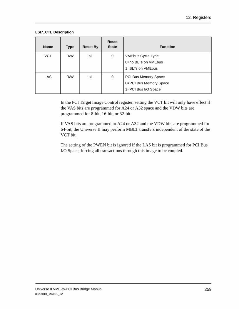
12. Registers
In the PCI Target Image Control register, setting the VCT bit will only have effect if the VAS bits are programmed for A24 or A32 space and the VDW bits are programmed for 8-bit, 16-bit, or 32-bit.
If VAS bits are programmed to A24 or A32 and the VDW bits are programmed for 64-bit, the Universe II may perform MBLT transfers independent of the state of the VCT bit.
The setting of the PWEN bit is ignored if the LAS bit is programmed for PCI Bus I/O Space, forcing all transactions through this image to be coupled.
VCT R/W all 0 VMEbus Cycle Type
0=no BLTs on VMEbus
1=BLTs on VMEbus
LAS R/W all 0 PCI Bus Memory Space
0=PCI Bus Memory Space
1=PCI Bus I/O Space
LSI7_CTL Description
Name Type Reset ByReset State Function
Universe II VME-to-PCI Bus Bridge Manual 25980A3010_MA001_02

12. Registers
12.2.46 PCI Target Image 7 Base Address Register (LSI7_BS)The base address specifies the lowest address in the address range that is decoded.
Table 82: PCI Target Image 7 Base Address Register (LSI7_BS)
Register Name: LSI7_BS Register Offset: 0x1E0
Bits Function
31-24 BS
23-16 BS
15-08 Reserved
07-00 Reserved
LSI7_BS Description
Name Type Reset ByReset State Function
BS[31:16] R/W all 0 Base Address
Universe II VME-to-PCI Bus Bridge Manual26080A3010_MA001_02

12. Registers
12.2.47 PCI Target Image 7 Bound Address Register (LSI7_BD)The addresses decoded in a slave image are those which are greater than or equal to the base address and less than the bound register. If the bound address is 0, then the addresses decoded are those greater than or equal to the base address.
The bound address for PCI Target Image 0 and PCI Target Image 4 have a 4Kbyte resolution. PCI Target Images 1, 2, 3, 5, 6, and 7 have a 64Kbyte resolution.
Table 83: PCI Target Image 7 Bound Address Register (LSI7_BD)
Register Name: LSI7_BD Register Offset: 0x1E4
Bits Function
31-24 BD
23-16 BD
15-08 Reserved
07-00 Reserved
LSI7_BD Description
Name Type Reset ByReset State Function
BD[31:16] R/W all 0 Bound Address
Universe II VME-to-PCI Bus Bridge Manual 26180A3010_MA001_02

12. Registers
12.2.48 PCI Target Image 7 Translation Offset (LSI7_TO)Address bits [31:16] generated on the VMEbus in response to an image decode are a two’s complement addition of address bits [31:16] on the PCI Bus and bits [31:16] of the image’s translation offset.
Table 84: PCI Target Image 7 Translation Offset (LSI7_TO)
Register Name: LSI7_TO Register Offset: 0x1E8
Bits Function
31-24 TO
23-16 TO
15-08 Reserved
07-00 Reserved
LSI7_TO Description
Name Type Reset ByReset State Function
TO[31:16] R/W all 0 Translation offset
Universe II VME-to-PCI Bus Bridge Manual26280A3010_MA001_02

12. Registers
12.2.49 DMA Transfer Control Register (DCTL)This register is programmed from either bus or is programmed by the DMAC when it loads the command packet.
The DMA only accesses PCI Bus Memory space.
Table 85: DMA Transfer Control Register (DCTL)
Register Name: DCTL Register Offset: 0x200
Bits Function
31-24 L2V Reserved
23-16 VDW Reserved VAS
15-08 PGM SUPER Reserved NO_
VINC
VCT
07-00 LD64EN Reserved
DCTL Description
Name Type Reset ByReset State Function
L2V R/W all 0 Direction
0=Transfer from VMEbus to PCI Bus
1=Transfer from PCI Bus to VMEbus
VDW R/W all 0 VMEbus Maximum Datawidth
00=8-bit data width
01=16 bit data width
10=32-bit data width
11=64-bit data width
VAS R/W all 0 VMEbus Address Space
000=A16
001=A24
010=A32
011= Reserved
100=Reserved
101=Reserved
110=User1
111=User2
Universe II VME-to-PCI Bus Bridge Manual 26380A3010_MA001_02

12. Registers
The VCT bit determines whether or not the Universe II VME Master will generate BLT transfers. The value of this bit only has meaning if the address space is A24 or A32 and the data width is not 64 bits. If the data width is 64 bits the Universe II may perform MBLT transfers independent of the state of the VCT bit.
PGM R/W all 0 Program/Data AM Code
00=Data
01=Program
others= Reserved
SUPER R/W all 0 Supervisor/User AM Code
00=Non-Privileged
01=Supervisor
others= Reserved
NO_VINC R/W all 0 VMEbus Non-Incrementing Mode (Non-Inc Mode)
0=disabled
1=enabled
VCT R/W all 0 VMEbus Cycle Type
0=no BLTs on VMEbus
1=BLTs on VMEbus
LD64EN R/W all 1 Enable 64-bit PCI Bus Transactions
0=Disable
1=Enable
DCTL Description
Name Type Reset ByReset State Function
Universe II VME-to-PCI Bus Bridge Manual26480A3010_MA001_02

12. Registers
12.2.50 DMA Transfer Byte Count Register (DTBC)This register specifies the number of bytes to be moved by the DMA before the start of the DMA transfer, or the number of remaining bytes in the transfer while the DMA is active. This register is programmed from either bus or is programmed by the DMA Controller when it loads a command packet from a linked-list.
In direct mode the user must reprogram the DTBC register before each transfer.
When using the DMA to perform linked-list transfers, it is essential that the DTBC register contains a value of zero before setting the GO bit of the DGCS register or undefined behaviors may occur.
Table 86: DMA Transfer Byte Count Register (DTBC)
Register Name: DTBC Register Offset: 0x204
Bits Function
31-24 Reserved
23-16 DTBC
15-08 DTBC
07-00 DTBC
DTBC Description
Name Type Reset ByReset State Function
DTBC
[23:0]
R/W all 0 DMA Transfer Byte Count
Universe II VME-to-PCI Bus Bridge Manual 26580A3010_MA001_02

12. Registers
12.2.51 DMA PCI Bus Address Register (DLA)This register is programmed from either bus or by the DMA Controller when it loads a command packet. In direct mode the user must reprogram the DLA register before each transfer. In linked-list mode, this register is only updated when the DMA is stopped, halted, or at the completion of processing a command packet.
After a Bus Error, a Target-Abort, or a Master-Abort, the value in the DLA register must not be used to reprogram the DMA because it has no usable information. Some offset from its original value must be used.
Address bits [2:0] must be programmed the same as those in the DVA.
Table 87: DMA PCI Bus Address Register (DLA)
Register Name: DLA Register Offset: 0x208
Bits Function
31-24 LA
23-16 LA
15-08 LA
07-00 LA
DLA Description
Name Type Reset ByReset State Function
LA[31:3] R/W all 0 PCI Bus Address
LA[2:0] R/W all 0 PCI Bus Address
Universe II VME-to-PCI Bus Bridge Manual26680A3010_MA001_02

12. Registers
12.2.52 DMA VMEbus Address Register (DVA)This register is programmed from either bus or is programmed by the DMA Controller when it loads a command packet. In direct mode the user must reprogram the DVA register before each transfer. In linked-list operation, this register is only updated when the DMA is stopped, halted, or at the completion of processing a command packet.
After a bus error, a Target-Abort, or a Master-Abort, the value in the DVA register must not be used to reprogram the DMA because it has no usable information. Some offset from its original value must be used.
Address bits [2:0] must be programmed the same as those in the DLA.
Table 88: DMA VMEbus Address Register (DVA)
Register Name: DVA Register Offset: 0x210
Bits Function
31-24 VA
23-16 VA
15-08 VA
07-00 VA
DVA Description
Name Type Reset ByReset State Function
VA[31:0] R/W all 0 VMEbus Address
Universe II VME-to-PCI Bus Bridge Manual 26780A3010_MA001_02

12. Registers
12.2.53 DMA Command Packet Pointer (DCPP)This register contains the pointer into the current command packet. Initially it is programmed to the starting packet of the linked-list, and is updated with the address to a new command packet at the completion of a packet.
The packets must be aligned to a 32-byte address.
Table 89: DMA Command Packet Pointer (DCPP)
Register Name: DCPP Register Offset: 0x218
Bits Function
31-24 DCPP
23-16 DCPP
15-08 DCPP
07-00 DCPP Reserved
DCPP Description
Name Type Reset ByReset State Function
DCPP[31:5]
R/W all 0 DMA Command Packet Pointer
Universe II VME-to-PCI Bus Bridge Manual26880A3010_MA001_02

12. Registers
12.2.54 DMA General Control/Status Register (DGCS)Table 90: DMA General Control/Status Register (DGCS)
Register Name: DGCS Register Offset: 0x220
Bits Function
31-24 GO STOP_
REQ
HALT_
REQ
0 CHAIN 0 0 0
23-16 Reserved VON VOFF
15-08 ACT STOP HALT 0 DONE LERR VERR P_ERR
07-00 0 INT_
STOP
INT_
HALT
0 INT_
DONE
INT_
LERR
INT_
VERR
INT_
P_ERR
DGCS Description
Name Type Reset By Reset State Function
GO W/Read 0 always
all 0 DMA Go Bit
0=No effect
1=Enable DMA Transfers
STOP_
REQ
W/Read 0 always
all 0 DMA Stop Request
0=No effect
1=Stop DMA transfer when all buffered data has been written
HALT_
REQ
W/Read 0 always
all 0 DMA Halt Request
0=No effect
1=Halt the DMA transfer at the completion of the current command packet
CHAIN R/W all 0 DMA Chaining
0=DMA Direct Mode
1=DMA Linked List mode
Universe II VME-to-PCI Bus Bridge Manual 26980A3010_MA001_02

12. Registers
VON [2:0] R/W all 0 VMEbus “On” counter
000=Until done
001=256 bytes
010=512 bytes
011=1024 bytes
100=2048 bytes
101=4096 bytes
110=8192 bytes
111=16384 bytes
others= Reserved
VOFF [3:0] R/W all 0 VMEbus “Off” Counter
0000=0µs
0001=16µs
0010=32µs
0011=64µs
0100=128µs
0101=256µs
0110=512µs
0111=1024µs
1000=2µs
1001=4µs
1010=8µs
others= Reserved
ACT R all 0 DMA Active Status Bit
0=Not Active
1=Active
STOP R/Write 1 to Clear
all 0 DMA Stopped Status Bit
0=Not Stopped
1=Stopped
HALT R/Write 1 to Clear
all 0 DMA Halted Status Bit
0=Not Halted
1=Halted
DGCS Description
Name Type Reset By Reset State Function
Universe II VME-to-PCI Bus Bridge Manual27080A3010_MA001_02

12. Registers
DONE R/Write 1 to Clear
all 0 DMA Done Status Bit
0=Not Complete
1=Complete
LERR R/Write 1 to Clear
all 0 DMA PCI Bus Error Status Bit
0=No Error
1=Error
VERR R/Write 1 to Clear
all 0 DMA VMEbus Error Status Bit
0=No Error
1=Error
P_ERR R/Write 1 to Clear
all 0 DMA Programming Protocol Error Status Bit
Asserted if PCI master interface disabled or lower three bits of PCI and VME addresses differ
0=No Error
1=Error
INT_STOP R/W all 0 Interrupt when Stopped
0=Disable
1=Enable
INT_HALT R/W all 0 Interrupt when Halted
0=Disable
1=Enable
INT_
DONE
R/W all 0 Interrupt when Done
0=Disable
1=Enable
INT_LERR R/W all 0 Interrupt on LERR
0=Disable
1=Enable
INT_VERR R/W all 0 Interrupt on VERR
0=Disable
1=Enable
INT_P_
ERR
R/W all 0 Interrupt on Master Enable Error
0=Disable
1=Enable
DGCS Description
Name Type Reset By Reset State Function
Universe II VME-to-PCI Bus Bridge Manual 27180A3010_MA001_02

12. Registers
STOP, HALT, DONE, LERR, VERR, and P_ERR must be cleared before the GO bit is enabled.
Universe II VME-to-PCI Bus Bridge Manual27280A3010_MA001_02

12. Registers
12.2.55 DMA Linked List Update Enable Register (D_LLUE)
The PCI Resource must read back a logic 1 in the UPDATE field before proceeding to modify the linked list. After the Linked List has been modified the PCI Resource must clear the UPDATE field by writing a logic 0. The Universe II does not prevent an external master, from the PCI bus or the VMEbus, from writing to the other DMA registers (see “Linked-list Updating” on page 120).
Table 91: DMA Linked List Update Enable Register (D_LLUE)
Register Name: D_LLUE Register Offset: 0x224
Bits Function
31-24 UPDATE Reserved
23-16 Reserved
15-08 Reserved
07-00 Reserved
D_LLUE Description
Name Type Reset ByReset State Function
UPDATE R/W all 0 DMA Linked List Update Enable
0=PCI Resource not Updating Linked List
1=PCI Resource Updating Linked List
Universe II VME-to-PCI Bus Bridge Manual 27380A3010_MA001_02

12. Registers
12.2.56 PCI Interrupt Enable Register (LINT_EN) Table 92: PCI Interrupt Enable Register (LINT_EN)
Register Name: LINT_EN Register Offset: 0x300
Bits Function
31-24 Reserved
23-16 LM3 LM2 LM1 LM0 MBOX3 MBOX2 MBOX1 MBOX0
15-08 ACFAIL SYSFAIL SW_INT SW_
IACK
Reserved VERR LERR DMA
07-00 VIRQ7 VIRQ6 VIRQ5 VIRQ4 VIRQ3 VIRQ2 VIRQ1 VOWN
LINT_EN Description
Name Type Reset ByReset State Function
LM3 R/W all 0 Location Monitor 3
0=LM3 Interrupt Disabled
1=LM3 Interrupt Enabled
LM2 R/W all 0 Location Monitor 2
0=LM2 Interrupt Disabled
1=LM2 Interrupt Enabled
LM1 R/W all 0 Location Monitor 1
0=LM1 Interrupt Disabled
1=LM1 Interrupt Enabled
LM0 R/W all 0 Location Monitor 0
0=LM0 Interrupt Disabled
1=LM0 Interrupt Enabled
MBOX3 R/W all 0 Mailbox 3
0=MBOX3 Interrupt Disabled
1=MBOX3 Interrupt Enabled
MBOX2 R/W all 0 Mailbox 2
0=MBOX2 Interrupt Disabled
1=MBOX2 Interrupt Enabled
Universe II VME-to-PCI Bus Bridge Manual27480A3010_MA001_02

12. Registers
MBOX1 R/W all 0 Mailbox 1
0=MBOX1 Interrupt Disabled
1=MBOX1 Interrupt Enabled
MBOX0 R/W all 0 Mailbox 0
0=MBOX0 Interrupt Disabled
1=MBOX0 Interrupt Enabled
ACFAIL R/W all 0 ACFAIL Interrupt
0=ACFAIL Interrupt Disabled
1=ACFAIL Interrupt Enabled
SYSFAIL R/W all 0 SYSFAIL Interrupt
0=SYSFAIL Interrupt Disabled
1=SYSFAIL Interrupt Enabled
SW_INT R/W all 0 Local Software Interrupt
0=PCI Software Interrupt Disabled
1=PCI Software Interrupt Enabled
A zero-to-one transition will cause the PCI software interrupt to be asserted. Subsequent zeroing of this bit will cause the interrupt to be masked, but will not clear the PCI Software Interrupt Status bit.
SW_IACK R/W all 0 “VME Software IACK”
0 =“VME Software IACK” Interrupt Disabled
1 =“VME Software IACK” Interrupt Enabled
VERR R/W all 0 PCI VERR Interrupt
0 =PCI VERR Interrupt Disabled
1=PCI VERR Interrupt Enabled
LERR R/W all 0 PCI LERR Interrupt
0 =PCI LERR Interrupt Disabled
1 =PCI LERR Interrupt Enabled
DMA R/W all 0 PCI DMA Interrupt
0=PCI DMA Interrupt Disabled
1=PCI DMA Interrupt Enabled
LINT_EN Description
Name Type Reset ByReset State Function
Universe II VME-to-PCI Bus Bridge Manual 27580A3010_MA001_02

12. Registers
Bits VIRQ7-VIRQ1 enable the Universe II to respond as a VME Interrupt Handler to interrupts on the VIRQ[x] lines. When a VIRQx interrupt is enabled, and the corresponding VIRQ[x] pin is asserted, the Universe II requests the VMEbus and performs a VME IACK cycle for that interrupt level. When the interrupt acknowledge cycle completes, the STATUS/ID is stored in the corresponding VINT_ID register, the VIRQx bit of the LINT_STAT register is set, and a PCI interrupt is generated. The Universe II does not acquire further interrupt STATUS/ID vectors at the same interrupt level until the VIRQx bit in the LINT_STAT register is cleared.
The other bits enable the respective internal or external sources to interrupt the PCI side.
VIRQ7-VIRQ1
R/W all 0 VIRQx Interrupt
0=VIRQx Interrupt Disabled
1 =VIRQx Interrupt Enabled
VOWN R/W all 0 VOWN Interrupt
0=VOWN Interrupt Disabled
1=VOWN Interrupt Enabled
LINT_EN Description
Name Type Reset ByReset State Function
Universe II VME-to-PCI Bus Bridge Manual27680A3010_MA001_02

12. Registers
12.2.57 PCI Interrupt Status Register (LINT_STAT)Status bits indicated as “R/Write 1 to Clear” are edge sensitive: the status is latched when the interrupt event occurs. These status bits can be cleared independently of the state of the interrupt source by writing a “1” to the status register. Clearing the status bit does not imply the source of the interrupt is cleared. However, ACFAIL and SYSFAIL are level-sensitive. Clearing ACFAIL or SYSFAIL while their respective pins are still asserted will have no effect.
Table 93: PCI Interrupt Status Register (LINT_STAT)
Register Name: LINT_STAT Register Offset: 0x304
Bits Function
31-24 Reserved
23-16 LM3 LM2 LM1 LM0 MBOX3 MBOX2 MBOX1 MBOX0
15-08 ACFAIL SYSFAIL SW_INT SW_
IACK
Reserved VERR LERR DMA
07-00 VIRQ7 VIRQ6 VIRQ5 VIRQ4 VIRQ3 VIRQ2 VIRQ1 VOWN
LINT_STAT Description
Name Type Reset ByReset State Function
LM3 R/Write 1 to
Clear
all 0 Location Monitor 3 Status/Clear0=no Location Monitor 3 Interrupt,
1=Location Monitor 3 Interrupt active
LM2 R/Write 1 to
Clear
all 0 Location Monitor 2 Status/Clear0=no Location Monitor 2 Interrupt,
1=Location Monitor 2 Interrupt active
LM1 R/Write 1 to
Clear
all 0 Location Monitor 1 Status/Clear0=no Location Monitor 1 Interrupt,
1=Location Monitor 1 Interrupt active
LM0 R/Write 1 to
Clear
all 0 Location Monitor 0 Status/Clear0=no Location Monitor 0 Interrupt,
1=Location Monitor 0 Interrupt active
Universe II VME-to-PCI Bus Bridge Manual 27780A3010_MA001_02

12. Registers
MBOX3 R/Write 1 to
Clear
all 0 Mailbox 3 Status/Clear0=no Mailbox 3 Interrupt,
1=Mailbox 3 Interrupt active
MBOX2 R/Write 1 to
Clear
all 0 Mailbox 2 Status/Clear0=no Mailbox 2 Interrupt,
1=Mailbox 2 Interrupt active
MBOX1 R/Write 1 to
Clear
all 0 Mailbox 1 Status/Clear0=no Mailbox 1 Interrupt,
1=Mailbox 1 Interrupt active
MBOX0 R/Write 1 to
Clear
all 0 Mailbox 0 Status/Clear0=no Mailbox 0 Interrupt,
1=Mailbox 0 Interrupt active
ACFAIL R/Write 1 to
Clear
all 0 ACFAIL Interrupt Status/Clear
0=no ACFAIL Interrupt,
1=ACFAIL Interrupt active
SYSFAIL R/Write 1 to
Clear
all 0 SYSFAIL Interrupt Status/Clear
0=no SYSFAIL Interrupt,
1=SYSFAIL Interrupt active
SW_INT R/Write 1 to
Clear
all 0 Local Software Interrupt Status/Clear
0=no PCI Software Interrupt,
1=PCI Software Interrupt active
SW_IACK R/Write 1 to
Clear
all 0 “VME Software IACK” Status/Clear
0=no “VME Software IACK” Interrupt,
1=“VME Software IACK” Interrupt active
VERR R/Write 1 to
Clear
all 0 Local VERR Interrupt Status/Clear
0=Local VERR Interrupt masked,
1=Local VERR Interrupt active
LERR R/Write 1 to
Clear
all 0 Local LERR Interrupt Status/Clear
0=Local LERR Interrupt masked,
1=Local LERR Interrupt active
LINT_STAT Description
Name Type Reset ByReset State Function
Universe II VME-to-PCI Bus Bridge Manual27880A3010_MA001_02

12. Registers
DMA R/Write 1 to
Clear
all 0 Local DMA Interrupt Status/Clear
0=Local DMA Interrupt masked,
1=Local DMA Interrupt active
VIRQ7-VIRQ1
R/Write 1 to
Clear
all 0 VIRQx Interrupt Status/Clear
0=VIRQx Interrupt masked,
1=VIRQx Interrupt active
VOWN R/Write 1 to
Clear
all 0 VOWN Interrupt Status/Clear
0=no VOWN Interrupt masked,
1=VOWN Interrupt active
LINT_STAT Description
Name Type Reset ByReset State Function
Universe II VME-to-PCI Bus Bridge Manual 27980A3010_MA001_02

12. Registers
12.2.58 PCI Interrupt Map 0 Register (LINT_MAP0)This register maps various interrupt sources to one of the eight PCI interrupt pins. For example, a value of 000 maps the corresponding interrupt source to LINT_ [0].
Table 94: PCI Interrupt Map 0 Register (LINT_MAP0)
Register Name: LINT_MAP0 Register Offset: 0x308
Bits Function
31-24 Reserved VIRQ7 Reserved VIRQ6
23-16 Reserved VIRQ5 Reserved VIRQ4
15-08 Reserved VIRQ3 Reserved VIRQ2
07-00 Reserved VIRQ1 Reserved VOWN
LINT_MAP0 Description
Name Type Reset ByReset State Function
VIRQ7-VIRQ1
R/W all 0 PCI interrupt destination (LINT[7:0]) for VIRQx
VOWN R/W all 0 VMEbus ownership bit interrupt map to PCI interrupt
Universe II VME-to-PCI Bus Bridge Manual28080A3010_MA001_02

12. Registers
12.2.59 PCI Interrupt Map 1 Register (LINT_MAP1)This register maps various interrupt sources to one of the eight PCI interrupt pins. For example, a value of 000 maps the corresponding interrupt source to LINT_ [0].
Table 95: PCI Interrupt Map 1 Register (LINT_MAP1)
Register Name: LINT_MAP1 Register Offset: 0x30C
Bits Function
31-24 Reserved ACFAIL Reserved SYSFAIL
23-16 Reserved SW_INT Reserved SW_IACK
15-08 Reserved VERR
07-00 Reserved LERR Reserved DMA
LINT_MAP1 Description
Name Type Reset ByReset State Function
ACFAIL R/W all 0 ACFAIL interrupt destination
SYSFAIL R/W all 0 SYSFAIL interrupt destination
SW_INT R/W all 0 PCI software interrupt destination
SW_IACK R/W all 0 VMEbus Software IACK interrupt destination
VERR R/W all 0 VMEbus Error interrupt destination
LERR R/W all 0 PCI Bus Error interrupt destination
DMA R/W all 0 DMA interrupt destination
Universe II VME-to-PCI Bus Bridge Manual 28180A3010_MA001_02

12. Registers
12.2.60 VMEbus Interrupt Enable Register (VINT_EN)This register enables the various sources of VMEbus interrupts.
SW_INT can be enabled with the VME64AUTO power-up option.
Table 96: VMEbus Interrupt Enable Register (VINT_EN)
Register Name: VINT_EN Register Offset: 0x310
Bits Function
31-24 SW_
INT7
SW_
INT6
SW_
INT5
SW_
INT4
SW_
INT3
SW_
INT2
SW_
INT1
Reserved
23-16 Reserved MBOX3 MBOX2 MBOX1 MBOX0
15-08 Reserved SW_INT Reserved VERR LERR DMA
07-00 LINT7 LINT6 LINT5 LINT4 LINT3 LINT2 LINT1 LINT0
VINT_EN Description
Name Type Reset ByReset State Function
SW_INT7 R/W all 0 VME Software 7 Interrupt Mask0=VME Software 7 Interrupt masked,
1=VME Software 7 Interrupt enabledA zero-to-one transition will cause a VME level 7 interrupt to be generated. Subsequent zeroing of this bit will cause the interrupt to be masked, but will not clear the VME Software 7 Interrupt Status bit.
SW_INT6 R/W all 0 VME Software 6 Interrupt Mask0=VME Software 6 Interrupt masked,
1=VME Software 6 Interrupt enabledA zero-to-one transition will cause a VME level 6 interrupt to be generated. Subsequent zeroing of this bit will cause the interrupt to be masked, but will not clear the VME Software 6 Interrupt Status bit.
SW_INT5 R/W all 0 VME Software 5 Interrupt Mask0=VME Software 5 Interrupt masked,
1=VME Software 5 Interrupt enabledA zero-to-one transition will cause a VME level 5 interrupt to be generated. Subsequent zeroing of this bit will cause the interrupt to be masked, but will not clear the VME Software 5 Interrupt Status bit.
Universe II VME-to-PCI Bus Bridge Manual28280A3010_MA001_02

12. Registers
SW_INT4 R/W all 0 VME Software 4 Interrupt Mask0=VME Software 4 Interrupt masked,
1=VME Software 4 Interrupt enabledA zero-to-one transition will cause a VME level 4 interrupt to be generated. Subsequent zeroing of this bit will cause the interrupt to be masked, but will not clear the VME Software 4 Interrupt Status bit.
SW_INT3 R/W all 0 VME Software 3 Interrupt Mask0=VME Software 3 Interrupt masked,
1=VME Software 3 Interrupt enabledA zero-to-one transition will cause a VME level 3 interrupt to be generated. Subsequent zeroing of this bit will cause the interrupt to be masked, but will not clear the VME Software 3 Interrupt Status bit.
SW_INT2 R/W all 0 VME Software 2 Interrupt Mask0=VME Software 2 Interrupt masked,
1=VME Software 2 Interrupt enabledA zero-to-one transition will cause a VME level 2 interrupt to be generated. Subsequent zeroing of this bit will cause the interrupt to be masked, but will not clear the VME Software 2 Interrupt Status bit.
SW_INT1 R/W all 0 VME Software 1 Interrupt Mask0=VME Software 1 Interrupt masked,
1=VME Software 1 Interrupt enabledA zero-to-one transition will cause a VME level 1 interrupt to be generated. Subsequent zeroing of this bit will cause the interrupt to be masked, but will not clear the VME Software 1 Interrupt Status bit.
MBOX3 R/W all 0 Mailbox 3 Mask
0=MBOX3 Interrupt masked,
1=MBOX3 Interrupt enabled
MBOX2 R/W all 0 Mailbox 2 Mask
0=MBOX2 Interrupt masked,
1=MBOX2 Interrupt enabled
MBOX1 R/W all 0 Mailbox 1 Mask
0=MBOX1 Interrupt masked,
1=MBOX1 Interrupt enabled
VINT_EN Description
Name Type Reset ByReset State Function
Universe II VME-to-PCI Bus Bridge Manual 28380A3010_MA001_02

12. Registers
MBOX0 R/W all 0 Mailbox 0 Mask
0=MBOX0 Interrupt masked,
1=MBOX0 Interrupt enabled
SW_INT R/W all Power-up Option
“VME Software Interrupt” Mask
0 = VME Software Interrupt masked
1 =VME Software Interrupt enabled
A zero-to-one transition causes the VME software interrupt to be asserted. Subsequent zeroing of this bit causes the interrupt to be masked and the VMEbus interrupt negated, but does not clear the VME software interrupt status bit.
VERR R/W all 0 VERR Interrupt Mask
0 =PCI VERR Interrupt masked
1=PCI VERR Interrupt enabled
LERR R/W all 0 LERR Interrupt Mask
0 =PCI LERR Interrupt masked
1 =PCI LERR Interrupt enabled
DMA R/W all 0 DMA Interrupt Mask
0=PCI DMA Interrupt masked
1=PCI DMA Interrupt enabled
LINT7-LINT0 R/W all 0 PCI Interrupt Mask
0=LINTx Interrupt masked
1 =LINTx Interrupt enabled
VINT_EN Description
Name Type Reset ByReset State Function
Universe II VME-to-PCI Bus Bridge Manual28480A3010_MA001_02

12. Registers
12.2.61 VMEbus Interrupt Status Register (VINT_STAT)This register maps PCI Bus interrupt sources to one of the seven VMEbus interrupt pins. A value of 001 maps the corresponding interrupt source to VIRQ*[1], a value of 002 maps to VIRQ*[2], etc. A value of 000 effectively masks the interrupt since there is no corresponding VIRQ*[0].
Table 97: VMEbus Interrupt Status Register (VINT_STAT)
Register Name: VINT_STAT Register Offset: 0x314
Bits Function
31-24 SW_
INT7
SW_
INT6
SW_
INT5
SW_
INT4
SW_
INT3
SW_
INT2
SW_
INT1
Reserved
23-16 Reserved MBOX3 MBOX2 MBOX1 MBOX0
15-08 Reserved SW_INT Reserved VERR LERR DMA
07-00 LINT7 LINT6 LINT5 LINT4 LINT3 LINT2 LINT1 LINT0
VINT_STAT Description
Name Type Reset ByReset State Function
SW_INT7 R/Write 1 to clear
all 0 VME Software 7 Interrupt Status/Clear0=no VME Software 7 Interrupt,
1=VME Software 7 Interrupt active
SW_INT6 R/Write 1 to clear
all 0 VME Software 6 Interrupt Status/Clear0=no VME Software 6 Interrupt,
1=VME Software 6 Interrupt active
SW_INT5 R/Write 1 to clear
all 0 VME Software 5 Interrupt Status/Clear0=no VME Software 5 Interrupt,
1=VME Software 5 Interrupt active
SW_INT4 R/Write 1 to clear
all 0 VME Software 4 Interrupt Status/Clear0=no VME Software 4 Interrupt,
1=VME Software 4 Interrupt active
SW_INT3 R/Write 1 to clear
all 0 VME Software 3 Interrupt Status/Clear0=no VME Software 3 Interrupt,
1=VME Software 3 Interrupt active
Universe II VME-to-PCI Bus Bridge Manual 28580A3010_MA001_02

12. Registers
SW_INT2 R/Write 1 to clear
all 0 VME Software 2 Interrupt Status/Clear0=no VME Software 2 Interrupt,
1=VME Software 2 Interrupt active
SW_INT1 R/Write 1 to clear
all 0 VME Software 1 Interrupt Status/Clear0=no VME Software 1 Interrupt,
1=VME Software 1 Interrupt active
MBOX3 R/Write 1 to clear
all 0 Mailbox 3 Status/Clear0=no Mailbox 3 Interrupt,
1=Mailbox 3 Interrupt active
MBOX2 R/Write 1 to clear
all 0 Mailbox 2 Status/Clear0=no Mailbox 2 Interrupt,
1=Mailbox 2 Interrupt active
MBOX1 R/Write 1 to clear
all 0 Mailbox 1 Status/Clear0=no Mailbox 1 Interrupt,
1=Mailbox 1 Interrupt active
MBOX0 R/Write 1 to clear
all 0 Mailbox 0 Status/Clear0=no Mailbox 0 Interrupt,
1=Mailbox 0 Interrupt active
SW_INT R/Write 1 to
Clear
all Power-up Option
VME Software Interrupt Status/Clear
0=VME Software Interrupt inactive,
1=VME Software Interrupt active
VERR R/Write 1 to
Clear
all 0 VERR Interrupt Status/Clear
0=VME VERR Interrupt masked,
1=VME VERR Interrupt enabled
LERR R/Write 1 to
Clear
all 0 LERR Interrupt Status/Clear
0=VME LERR Interrupt masked,
1=VME LERR Interrupt enabled
DMA R/Write 1 to
Clear
all 0 DMA Interrupt Status/Clear
0=VME DMA Interrupt masked,
1=VME DMA Interrupt enabled
LINT7-LINT0 R/Write 1 to
Clear
all 0 LINTx Interrupt Status/Clear
0=LINTx Interrupt masked,
1=LINTx Interrupt enabled
VINT_STAT Description
Name Type Reset ByReset State Function
Universe II VME-to-PCI Bus Bridge Manual28680A3010_MA001_02

12. Registers
12.2.62 VME Interrupt Map 0 Register (VINT_MAP0)Table 98: VME Interrupt Map 0 Register (VINT_MAP0)
Register Name: VINT_MAP0 Register Offset: 0x318
Bits Function
31-24 Reserved LINT7 Reserved LINT6
23-16 Reserved LINT5 Reserved LINT4
15-08 Reserved LINT3 Reserved LINT2
07-00 Reserved LINT1 Reserved LINT0
VINT_MAP0 Description
Name Type Reset ByReset State Function
LINT7-LINT0[2:0]
R/W all 0 VMEbus destination of PCI Bus interrupt source
Universe II VME-to-PCI Bus Bridge Manual 28780A3010_MA001_02

12. Registers
12.2.63 VME Interrupt Map 1 Register (VINT_MAP1)This register maps VMEbus interrupt sources to one of the seven VMEbus interrupt pins. A value of 001 maps the corresponding interrupt source to VIRQ*[1], a value of 010 maps to VIRQ*[2], etc. A value of 000 effectively masks the interrupt since there is no corresponding VIRQ*[0].
SW_INT is set to 010 with the VME64AUTO power-up option.
Table 99: VME Interrupt Map 1 Register (VINT_MAP1)
Register Name: VINT_MAP1 Register Offset: 0x31C
Bits Function
31-24 Reserved
23-16 Reserved SW_INT
15-08 Reserved VERR
07-00 Reserved LERR Reserved DMA
VINT_MAP1 Description
Name Type Reset ByReset State Function
SW_INT R/W all Power-up Option
VMEbus Software interrupt destination
VERR R/W all 0 VMEbus Error interrupt destination
LERR R/W all 0 PCI Bus Error interrupt destination
DMA R/W all 0 DMA interrupt destination
Universe II VME-to-PCI Bus Bridge Manual28880A3010_MA001_02

12. Registers
12.2.64 Interrupt STATUS/ID Out Register (STATID)When the Universe II responds to an interrupt acknowledge cycle on VMEbus it returns an 8-bit STATUS/ID. STATID [7:1] can be written by software to uniquely identify the VMEbus module within the system. STATID [0] is a value of 0 if the Universe II is generating a software interrupt (SW_IACK) at the same level as the interrupt acknowledge cycle, otherwise it is a value of 1.
The reset state is designed to support the VME64 Auto ID STATUS/ID value.
Table 100: Interrupt STATUS/ID Out Register (STATID)
Register Name: STATID Register Offset: 0x320
Bits Function
31-24 STATID [7:0]
23-16 Reserved
15-08 Reserved
07-00 Reserved
Name Type Reset ByReset State Function
STATID [7:1] R/W all 1111111 Bits [7:1] of the STATUS/ID byte are returned when the Universe II responds to a VMEbus IACK cycle.
STATID [0] R all See below 0 = the Universe II is generating a SW_IACK at the same level as the interrupt acknowledge cycle.
1 = the Universe II is not generating a SW_IACK at the same level as the interrupt acknowledge cycle.
Universe II VME-to-PCI Bus Bridge Manual 28980A3010_MA001_02

12. Registers
12.2.65 VIRQ1 STATUS/ID Register (V1_STATID)The Vx_STATID registers are read-only registers that hold the 8-bit VMEbus STATUS/ID that is acquired when the Universe II performs a IACK cycle for a given interrupt level.
The Universe II is enabled as the interrupt handler for a given interrupt level via the VIRQx bits of the LINT_EN register. Once a vector for a given level is acquired, the Universe II does not perform a subsequent interrupt acknowledge cycle at that level until the corresponding VIRQx bit in the LINT_STAT register is cleared.
The acquisition of a level x STATUS/ID by the Universe II updates the STATUS/ID field of the corresponding Vx_STATID register and generation of a PCI interrupt. A VMEbus error during the acquisition of the STATUS/ID vector sets the ERR bit, which means the STATUS/ID field may not contain a valid vector.
Table 101: VIRQ1 STATUS/ID Register (V1_STATID)
Register Name: V1_STATID Register Offset: 0x324
Bits Function
31-24 Reserved
23-16 Reserved
15-08 Reserved ERR
07-00 STATID [7:0]
V1_STATID Description
Name Type Reset ByReset State Function
ERR R all 0 Error Status Bit
0=STATUS/ID was acquired without bus error
1=bus error occurred during acquisition of the STATUS/ID
STATID [7:0] R all 0 STATUS/ID acquired during IACK cycle for level 1 VMEbus interrupt
Universe II VME-to-PCI Bus Bridge Manual29080A3010_MA001_02

12. Registers
12.2.66 VIRQ2 STATUS/ID Register (V2_STATID)The Vx_STATID registers are read-only registers that hold the 8-bit VMEbus STATUS/ID that is acquired when the Universe II performs a IACK cycle for a given interrupt level.
The Universe II is enabled as the interrupt handler for a given interrupt level via the VIRQx bits of the LINT_EN register. Once a vector for a given level is acquired, the Universe II does not perform a subsequent interrupt acknowledge cycle at that level until the corresponding VIRQx bit in the LINT_STAT register is cleared.
The acquisition of a level x STATUS/ID by the Universe II updates the STATUS/ID field of the corresponding Vx_STATID register and generation of a PCI interrupt. A VMEbus error during the acquisition of the STATUS/ID vector sets the ERR bit, which means the STATUS/ID field may not contain a valid vector.
Table 102: VIRQ2 STATUS/ID Register (V2_STATID)
Register Name: V2_STATID Register Offset: 0x328
Bits Function
31-24 Reserved
23-16 Reserved
15-08 Reserved ERR
07-00 STATID [7:0]
V2_STATID Description
Name Type Reset ByReset State Function
ERR R all 0 Error Status Bit
0=STATUS/ID was acquired without bus error
1=bus error occurred during acquisition of the STATUS/ID
STATID [7:0] R all 0 STATUS/ID acquired during IACK cycle for level 1 VMEbus interrupt
Universe II VME-to-PCI Bus Bridge Manual 29180A3010_MA001_02

12. Registers
12.2.67 VIRQ3 STATUS/ID Register (V3_STATID)The Vx_STATID registers are read-only registers that hold the 8-bit VMEbus STATUS/ID that is acquired when the Universe II performs a IACK cycle for a given interrupt level.
The Universe II is enabled as the interrupt handler for a given interrupt level via the VIRQx bits of the LINT_EN register. Once a vector for a given level is acquired, the Universe II does not perform a subsequent interrupt acknowledge cycle at that level until the corresponding VIRQx bit in the LINT_STAT register is cleared.
The acquisition of a level x STATUS/ID by the Universe II updates the STATUS/ID field of the corresponding Vx_STATID register and generation of a PCI interrupt. A VMEbus error during the acquisition of the STATUS/ID vector sets the ERR bit, which means the STATUS/ID field may not contain a valid vector.
Table 103: VIRQ3 STATUS/ID Register (V3_STATID)
Register Name: V3_STATID Register Offset: 0x32C
Bits Function
31-24 Reserved
23-16 Reserved
15-08 Reserved ERR
07-00 STATID [7:0]
V3_STATID Description
Name Type Reset ByReset State Function
ERR R all 0 Error Status Bit
0=STATUS/ID was acquired without bus error
1=bus error occurred during acquisition of the STATUS/ID
STATID [7:0] R all 0 STATUS/ID acquired during IACK cycle for level 3VMEbus interrupt
Universe II VME-to-PCI Bus Bridge Manual29280A3010_MA001_02

12. Registers
12.2.68 VIRQ4 STATUS/ID Register (V4_STATID)The Vx_STATID registers are read-only registers that hold the 8-bit VMEbus STATUS/ID that is acquired when the Universe II performs a IACK cycle for a given interrupt level.
The Universe II is enabled as the interrupt handler for a given interrupt level via the VIRQx bits of the LINT_EN register. Once a vector for a given level is acquired, the Universe II does not perform a subsequent interrupt acknowledge cycle at that level until the corresponding VIRQx bit in the LINT_STAT register is cleared.
The acquisition of a level x STATUS/ID by the Universe II updates the STATUS/ID field of the corresponding Vx_STATID register and generation of a PCI interrupt. A VMEbus error during the acquisition of the STATUS/ID vector sets the ERR bit, which means the STATUS/ID field may not contain a valid vector.
Table 104: VIRQ4 STATUS/ID Register (V4_STATID)
Register Name: V4_STATID Register Offset: 0x330
Bits Function
31-24 Reserved
23-16 Reserved
15-08 Reserved ERR
07-00 STATID [7:0]
V4_STATID Description
Name Type Reset ByReset State Function
ERR R all 0 Error Status Bit
0=STATUS/ID was acquired without bus error
1=bus error occurred during acquisition of the STATUS/ID
STATID [7:0] R all 0 STATUS/ID acquired during IACK cycle for level 4 VMEbus interrupt
Universe II VME-to-PCI Bus Bridge Manual 29380A3010_MA001_02

12. Registers
12.2.69 VIRQ5 STATUS/ID Register (V5_STATID)The Vx_STATID registers are read-only registers that hold the 8-bit VMEbus STATUS/ID that is acquired when the Universe II performs a IACK cycle for a given interrupt level.
The Universe II is enabled as the interrupt handler for a given interrupt level via the VIRQx bits of the LINT_EN register. Once a vector for a given level is acquired, the Universe II does not perform a subsequent interrupt acknowledge cycle at that level until the corresponding VIRQx bit in the LINT_STAT register is cleared.
The acquisition of a level x STATUS/ID by the Universe II updates the STATUS/ID field of the corresponding Vx_STATID register and generation of a PCI interrupt. A VMEbus error during the acquisition of the STATUS/ID vector sets the ERR bit, which means the STATUS/ID field may not contain a valid vector.
Table 105: VIRQ5 STATUS/ID Register (V5_STATID)
Register Name: V5_STATID Register Offset: 0x334
Bits Function
31-24 Reserved
23-16 Reserved
15-08 Reserved ERR
07-00 STATID [7:0]
V5_STATID Description
Name Type Reset ByReset State Function
ERR R all 0 Error Status Bit
0=STATUS/ID was acquired without bus error
1=bus error occurred during acquisition of the STATUS/ID
STATID [7:0] R all 0 STATUS/ID acquired during IACK cycle for level 5 VMEbus interrupt
Universe II VME-to-PCI Bus Bridge Manual29480A3010_MA001_02

12. Registers
12.2.70 VIRQ6 STATUS/ID Register (V6_STATID)The Vx_STATID registers are read-only registers that hold the 8-bit VMEbus STATUS/ID that is acquired when the Universe II performs a IACK cycle for a given interrupt level.
The Universe II is enabled as the interrupt handler for a given interrupt level via the VIRQx bits of the LINT_EN register. Once a vector for a given level is acquired, the Universe II does not perform a subsequent interrupt acknowledge cycle at that level until the corresponding VIRQx bit in the LINT_STAT register is cleared.
The acquisition of a level x STATUS/ID by the Universe II updates the STATUS/ID field of the corresponding Vx_STATID register and generation of a PCI interrupt. A VMEbus error during the acquisition of the STATUS/ID vector sets the ERR bit, which means the STATUS/ID field may not contain a valid vector.
Table 106: VIRQ6 STATUS/ID Register (V6_STATID)
Register Name: V6_STATID Register Offset: 0x338
Bits Function
31-24 Reserved
23-16 Reserved
15-08 Reserved ERR
07-00 STATID [7:0]
V6_STATID Description
Name Type Reset ByReset State Function
ERR R all 0 Error Status Bit
0=STATUS/ID was acquired without bus error
1=bus error occurred during acquisition of the STATUS/ID
STATID [7:0] R all 0 STATUS/ID acquired during IACK cycle for level 6 VMEbus interrupt
Universe II VME-to-PCI Bus Bridge Manual 29580A3010_MA001_02

12. Registers
12.2.71 VIRQ7 STATUS/ID Register (V7_STATID)The Vx_STATID registers are read-only registers that hold the 8-bit VMEbus STATUS/ID that is acquired when the Universe II performs a IACK cycle for a given interrupt level.
The Universe II is enabled as the interrupt handler for a given interrupt level via the VIRQx bits of the LINT_EN register. Once a vector for a given level is acquired, the Universe II does not perform a subsequent interrupt acknowledge cycle at that level until the corresponding VIRQx bit in the LINT_STAT register is cleared.
The acquisition of a level x STATUS/ID by the Universe II updates the STATUS/ID field of the corresponding Vx_STATID register and generation of a PCI interrupt. A VMEbus error during the acquisition of the STATUS/ID vector sets the ERR bit, which means the STATUS/ID field may not contain a valid vector.
Table 107: VIRQ7 STATUS/ID Register (V7_STATID)
Register Name: V7_STATID Register Offset: 0x33C
Bits Function
31-24 Reserved
23-16 Reserved
15-08 Reserved ERR
07-00 STATID [7:0]
V7_STATID Description
Name Type Reset ByReset State Function
ERR R all 0 Error Status Bit
0=STATUS/ID was acquired without bus error
1=bus error occurred during acquisition of the STATUS/ID
STATID [7:0] R all 0 STATUS/ID acquired during IACK cycle for level 7 VMEbus interrupt
Universe II VME-to-PCI Bus Bridge Manual29680A3010_MA001_02

12. Registers
12.2.72 PCI Interrupt Map 2 Register (LINT_MAP2)This register maps interrupt sources to one of the eight PCI interrupt pins. For example, a value of 000 maps the corresponding interrupt source to LINT_ [0].
Table 108: PCI Interrupt Map 2 Register (LINT_MAP2)
Register Name: LINT_MAP2 Register Offset: 0x340
Bits Function
31-24 Reserved LM3 Reserved LM2
23-16 Reserved LM1 Reserved LM0
15-08 Reserved MBOX3 Reserved MBOX2
07-00 Reserved MBOX1 Reserved MBOX0
LINT_MAP2 Description
Name Type Reset ByReset State Function
LM3 [2:0] R/W all 0 Location Monitor 3 Interrupt destination
LM2 [2:0] R/W all 0 Location Monitor 2 Interrupt destination
LM1 [2:0] R/W all 0 Location Monitor 1 Interrupt destination
LM0 [2:0] R/W all 0 Location Monitor 0 Interrupt destination
MBOX3 [2:0] R/W all 0 Mailbox 3 Interrupt destination
MBOX2 [2:0] R/W all 0 Mailbox 2 Interrupt destination
MBOX1 [2:0] R/W all 0 Mailbox 1 Interrupt destination
MBOX0 [2:0] R/W all 0 Mailbox 0 Interrupt destination
Universe II VME-to-PCI Bus Bridge Manual 29780A3010_MA001_02

12. Registers
12.2.73 VME Interrupt Map 2 Register (VINT_MAP2)This register maps interrupt sources to one of the seven VMEbus interrupt pins. A value of 001 maps the corresponding interrupt source to VIRQ*[1], a value of 002 maps to VIRQ*[2], etc. A value of 000 effectively masks the interrupt since there is no corresponding VIRQ*[0].
Table 109: VME Interrupt Map 2 Register (VINT_MAP2)
Register Name: VINT_MAP2 Register Offset: 0x344
Bits Function
31-24 Reserved
23-16 Reserved
15-08 Reserved MBOX3 Reserved MBOX2
07-00 Reserved MBOX1 Reserved MBOX0
VINT_MAP2 Description
Name Type Reset ByReset State Function
MBOX3 [2:0] R/W all 0 Mailbox 3 Interrupt destination
MBOX2 [2:0] R/W all 0 Mailbox 2 Interrupt destination
MBOX1 [2:0] R/W all 0 Mailbox 1 Interrupt destination
MBOX0 [2:0] R/W all 0 Mailbox 0 Interrupt destination
Universe II VME-to-PCI Bus Bridge Manual29880A3010_MA001_02

12. Registers
12.2.74 Mailbox 0 Register (MBOX0)This register is a general purpose mailbox register.
Table 110: Mailbox 0 Register (MBOX0)
Register Name: MBOX0 Register Offset: 0x348
Bits Function
31-24 MBOX0
23-16 MBOX0
15-08 MBOX0
07-00 MBOX0
DVA Description
Name Type Reset ByReset State Function
MBOX0 [31:0]
R/W all 0 Mailbox
Universe II VME-to-PCI Bus Bridge Manual 29980A3010_MA001_02

12. Registers
12.2.75 Mailbox 1 Register (MBOX1)This register is a general purpose mailbox register.
Table 111: Mailbox 1 Register (MBOX1)
Register Name: MBOX1 Register Offset: 0x34C
Bits Function
31-24 MBOX1
23-16 MBOX1
15-08 MBOX1
07-00 MBOX1
DVA Description
Name Type Reset ByReset State Function
MBOX1 [31:0]
R/W all 0 Mailbox
Universe II VME-to-PCI Bus Bridge Manual30080A3010_MA001_02

12. Registers
12.2.76 Mailbox 2 Register (MBOX2)This register is a general purpose mailbox register.
Table 112: Mailbox 2 Register (MBOX2)
Register Name: MBOX2 Register Offset: 0x350
Bits Function
31-24 MBOX2
23-16 MBOX2
15-08 MBOX2
07-00 MBOX2
DVA Description
Name Type Reset ByReset State Function
MBOX2 [31:0]
R/W all 0 Mailbox
Universe II VME-to-PCI Bus Bridge Manual 30180A3010_MA001_02

12. Registers
12.2.77 Mailbox 3 Register (MBOX3)This register is a general purpose mailbox register.
Table 113: Mailbox 3 Register (MBOX3)
Register Name: MBOX3 Register Offset: 0x354
Bits Function
31-24 MBOX3
23-16 MBOX3
15-08 MBOX3
07-00 MBOX3
DVA Description
Name Type Reset ByReset State Function
MBOX3 [31:0]
R/W all 0 Mailbox
Universe II VME-to-PCI Bus Bridge Manual30280A3010_MA001_02

12. Registers
12.2.78 Semaphore 0 Register (SEMA0)This register can only be accessed through byte-wide access.
If a semaphore bit is a value of 0, the associated tag field can be written to. If a semaphore bit is a value of 1, the associated tag field cannot be written to (see “Semaphores” on page 102).
Table 114: Semaphore 0 Register (SEMA0)
Register Name: SEMA0 Register Offset: 0x358
Bits Function
31-24 SEM3 TAG3
23-16 SEM2 TAG2
15-08 SEM1 TAG1
07-00 SEM0 TAG0
SEMA0 Description
Name Type Reset ByReset State Function
SEM3 R/W all 0 Semaphore 3
TAG3 [6:0] R/W all 0 Tag 3
SEM2 R/W all 0 Semaphore 2
TAG2 [6:0] R/W all 0 Tag2
SEM1 R/W all 0 Semaphore 1
TAG1 [6:0] R/W all 0 Tag 1
SEM0 R/W all 0 Semaphore 0
TAG0 [6:0] R/W all 0 Tag 0
Universe II VME-to-PCI Bus Bridge Manual 30380A3010_MA001_02

12. Registers
12.2.79 Semaphore 1 Register (SEMA1)This register can only be accessed through byte-wide access.
If a semaphore bit is a value of 0, the associated tag field can be written to. If a semaphore bit is a value of 1, the associated tag field cannot be written to (see “Semaphores” on page 102).
Table 115: Semaphore 1 Register (SEMA1)
Register Name: SEMA1 Register Offset: 0x35C
Bits Function
31-24 SEM7 TAG7
23-16 SEM6 TAG6
15-08 SEM5 TAG5
07-00 SEM4 TAG4
SEMA1 Description
Name Type Reset ByReset State Function
SEM3 R/W all 0 Semaphore 7
TAG3 [6:0] R/W all 0 Tag 7
SEM2 R/W all 0 Semaphore 6
TAG2 [6:0] R/W all 0 Tag 6
SEM1 R/W all 0 Semaphore 5
TAG1 [6:0] R/W all 0 Tag 5
SEM0 R/W all 0 Semaphore 4
TAG0 [6:0] R/W all 0 Tag 4
Universe II VME-to-PCI Bus Bridge Manual30480A3010_MA001_02

12. Registers
12.2.80 Master Control Register (MAST_CTL) Table 116: Master Control Register (MAST_CTL)
Register Name: MAST_CTL Register Offset: 0x400
Bits Function
31-24 MAXRTRY PWON
23-16 VRL VRM VREL VOWN VOWN_
ACK
Reserved
15-08 Reserved PABS Reserved
07-00 BUS_NO
MAST_CTL Description
Name Type Reset ByReset State Function
MAXRTRY [3:0]
R/W all 1000 Maximum Number of Retries
0000=Retry Forever, Multiples of 64 (0001 through 1111).
Maximum Number of retries before the PCI master interface signals error condition
PWON [3:0] R/W all 0000 Posted Write Transfer Count
0000=128 bytes, 0001=256 bytes, 0010=512 bytes, 0011=1024 bytes, 0100=2048 bytes, 0101=4096 bytes, 0110 - 1110 = Reserved, 1111=Early release of BBSY*.
Transfer count at which the PCI Slave Channel Posted Writes FIFO gives up the VME Master Interface.
VRL [1:0] R/W all 11 VMEbus Request Level
00=Level 0,01=Level 1,10=Level 2, 11=Level 3
VRM R/W all 0 VMEbus Request Mode
0=Demand,1=Fair
VREL R/W all 0 VMEbus Release Mode
0=Release When Done (RWD), 1=Release on Request (ROR)
VOWN R/W all 0 VME Ownership Bit
0=Release VMEbus, 1=Acquire and Hold VMEbus
Universe II VME-to-PCI Bus Bridge Manual 30580A3010_MA001_02

12. Registers
Writing a 1 to the VOWN bit in the MAST_CTL register has the effect of asserting BBSY* until a 0 is written to the VOWN bit. It does not affect the transactions in the PCI Target Channel. The Universe II will not do an early release of BBSY* if the VMEbus was owned during a transaction by means of VOWN, regardless of the value of PWON.
It is important to wait until VOWN_ACK is a value of 0 before writing a value of 1 to the VOWN bit.
In the event that BERR* is asserted on the VMEbus once the Universe II owns the VMEbus, the user must release ownership by programming the VOWN bit to a value of 0, if the VMEbus was gained by setting the VOWN bit. VMEbus masters must not write a value of 1 to the VOWN bit since this will lock up the VMEbus.
VOWN_ACK R all 0 VME Ownership Bit Acknowledge
0=VMEbus not owned, 1=VMEbus acquired and held due to assertion of VOWN
PABS [1:0] R/W all 00 PCI Aligned Burst Size
00=32 byte
01=64 byte
10=128 byte
11=256 byte
Controls the PCI address boundary at which the Universe II breaks up a PCI transaction in the VME Slave channel (see “VME Slave Image Programming” on page 84) and the DMA Channel (see “FIFO Operation and Bus Ownership” on page 121).
This field also determines when the PCI Master Module as part of the VME Slave Channel will request the PCI bus (i.e., when 32, 64,128, or 256 bytes are available). It does not have this effect on
BUS_NO [7:0]
R/W all 0000 0000 PCI Bus Number
MAST_CTL Description
Name Type Reset ByReset State Function
Universe II VME-to-PCI Bus Bridge Manual30680A3010_MA001_02

12. Registers
Once the value programmed in the PWON field is reached during dequeuing of posted writes, the Universe II will do an early release of BBSY*. If the PWON field is programmed to a value of 1111, the Universe II will do an early release of BBSY* at the completion of each transaction. Note that the VOWN setting described above overrides the POWN setting.
BUS_NO is used by the VMEbus Slave Channel when mapping VME transactions into PCI Configuration space. If the bus number of the VMEbus address (bits [23:16]) is equal to the BUS_NO field, then the Universe II generates a Type 0 configuration cycle, otherwise Type 1 is generated.
Universe II VME-to-PCI Bus Bridge Manual 30780A3010_MA001_02

12. Registers
12.2.81 Miscellaneous Control Register (MISC_CTL) Table 117: Miscellaneous Control Register (MISC_CTL)
Register Name: MISC_CTL Register Offset: 0x404
Bits Function
31-24 VBTO Reserved VARB VARBTO
23-16 SW_LRST
SW_SYSRST
Reserved BI ENGBI RE-
SCIND
SYSCON V64-
AUTO
15-08 Reserved SYSRE-SET
Reserved
07-00 Reserved
MISC_CTL Description
Name Type Reset ByReset State Function
VBTO R/W all 0011 VME Bus Time-out
0000=Disable
0001=16 µsec
0010=32 µsec
0011=64 µsec
0100=128 µsec
0101=256 µsec
0110=512 µsec
0111=1024 µsec
others= RESERVED
VARB R/W all 0 VMEbus Arbitration Mode
0=Round Robin
1=Priority
VARBTO R/W all 01 VMEbus Arbitration Time-out
00=Disable Timer
01=16 µs (minimum 8µs)
10=256 µs
others= Reserved
Universe II VME-to-PCI Bus Bridge Manual30880A3010_MA001_02

12. Registers
SW_LRST R/W all 0 Software PCI Reset
0=No effect
1=Initiate LRST_
A read always returns 0.
SW_
SYSRST
R/W all 0 Software VMEbus SYSRESET
0=No effect
1=Initiate SYSRST*
A read always returns 0.
BI R/W all Power-up Option
BI-Mode
0=Universe II is not in BI-Mode,
1=Universe II is in BI-Mode
Write to this bit to change the Universe II BI-Mode status. This bit is also affected by the global BI-Mode initiator VRIRQ1*, if this feature is enabled.
ENGBI R/W all 0 Enable Global BI-Mode Initiator
0=Assertion of VIRQ1 ignored
1=Assertion of VIRQ1 puts device in BI-Mode
RESCIND R/W all 1 RESCIND is unused in the Universe II.
SYSCON R/W all Power-up Option
SYSCON
0=Universe II is not VMEbus System Controller,
1=Universe II is VMEbus System Controller
V64AUTO R/W all Power-up Option
VME64 Auto ID
Write: 0=No effect
1=Initiate sequence
This bit initiates Universe II VME64 Auto ID Slave participation.
SYSRESET R/W all 0 System Reset
0=No effect
1=Initiate SYSRST*
Universe II asserts SYSRESET without resetting itself.
MISC_CTL Description
Name Type Reset ByReset State Function
Universe II VME-to-PCI Bus Bridge Manual 30980A3010_MA001_02
12. Registers
VMEbus masters must not write to SW_SYSRST, and PCI masters must not write to SW_LRST.
The bits VBTO, VARB and VARBTO support SYSCON functionality.
Universe II participation in the VME64 Auto ID mechanism is controlled by the VME64AUTO bit. When this bit is detected high, the Universe II uses the SW_IACK mechanism to generate VXIRQ2 on the VMEbus, then releases VXSYSFAIL. Access to the CR/CSR image is enabled when the level 2 interrupt acknowledge cycle completes. This sequence can be initiated with a power-up option or by software writing a 1 to this bit.
Universe II VME-to-PCI Bus Bridge Manual31080A3010_MA001_02

12. Registers
12.2.82 Miscellaneous Status Register (MISC_STAT) Table 118: Miscellaneous Status Register (MISC_STAT)
Register Name: MISC_STAT Register Offset: 0x408
Bits Function
31-24 Reserved LCLSIZE Reserved DY4AUTO
Reserved
23-16 Reserved MYBBSY Reserved DY4_DONE
TXFE RXFE Reserved
15-08 DY4AUTOID
07-00 Reserved
MISC_STAT Description
Name Type Reset ByReset State Function
LCLSIZE R all Power-up Option
PCI Bus Size
At the rising edge of RST_, the Universe II samples REQ64_ to determine the PCI Bus size. This bit reflects the result.
0=32-bit
1=64-bit
DY4AUTO R all Power-up Option
DY4 Auto ID Enable
0=Disable
1=Enable
MYBBSY R all 1 Universe II BBSY
0=Asserted
1=Negated
DY4DONE R all 0 DY4 Auto ID Done
0=Not done
1=Done
TXFE R all 1 PCI Target Channel Posted Writes FIFO
0=data in the FIFO
1=no data in the FIFO
Universe II VME-to-PCI Bus Bridge Manual 31180A3010_MA001_02

12. Registers
RXFE R all 1 VME Slave Channel Posted Writes FIFO
0=data in the FIFO
1=no data in the FIFO
DY4
AUTOID
R Power-up reset and VMEbus
SYS-
RESET*
0 DY4 Auto ID
MISC_STAT Description
Name Type Reset ByReset State Function
Universe II VME-to-PCI Bus Bridge Manual31280A3010_MA001_02

12. Registers
12.2.83 User AM Codes Register (USER_AM)The USER_AM register can only be used to generate and accept AM codes 0x10 through 0x1F. These AM codes are designated as USERAM codes in the VMEbus Specification.
Table 119: User AM Codes Register (USER_AM)
Register Name: USER_AM Register Offset: 0x40C
Bits Function
31-24 0 1 USER1AM Reserved
23-16 0 1 USER2AM Reserved
15-08 Reserved
07-00 Reserved
USER_AM Description
Name Type Reset ByReset State Function
USER1AM [3:0]
R/W all 0000 User AM Code 1
USER2AM [3:0]
R/W all 0000 User AM Code 2
Universe II VME-to-PCI Bus Bridge Manual 31380A3010_MA001_02

12. Registers
12.2.84 Universe II Specific Register (U2SPEC) Table 120: Universe II Specific Register (U2SPEC)
Register Name: U2SPEC Register Offset: 0x4FC
Bits Function
31-24 Universe Reserved
23-16 Universe Reserved
15-08 Universe Reserved
DS0/DS1 AS DTKFLTR
Reserved MASt11 READt27
07-00 Universe Reserved POSt28 Reserved PREt28
U2SPEC Description
Name TypeReset
ByReset State Function
DS0/DS1 R/W all 0 Data Strobe Filtering
0=Disable
1=Enable
AS R/W all 0 Address Strobe Filtering
0=Disable
1=Enable
DTKFLTR R/W all 0 VME DTACK* Inactive Filter
0=Slower but better filter
1=Faster but poorer filter
MASt11 R/W all 0 VME Master Parameter t11 Control (DS* high time during BLT’s and MBLT’s)
0=Default
1=Faster
READt27 R/W all 00 VME Master Parameter t27 Control (Delay of DS* negation after read)
00=Default
01=Faster
10=No Delay
Universe II VME-to-PCI Bus Bridge Manual31480A3010_MA001_02

12. Registers
POSt28 R/W all 0 VME Slave Parameter t28 Control (Time of DS* to DTACK* for posted-write)
0=Default
1=Faster
PREt28 R/W all 0 VME Slave Parameter t28 Control (Time of DS* to DTACK* for prefetch read)
0=Default
1=Faster
U2SPEC Description
Name TypeReset
ByReset State Function
Universe II VME-to-PCI Bus Bridge Manual 31580A3010_MA001_02

12. Registers
12.2.85 VMEbus Slave Image 0 Control (VSI0_CTL)This register provides the general, VMEbus and PCI controls for this slave image. Note that only transactions destined for PCI Memory space are decoupled (the posted write RXFIFO generates on Memory space transactions on the PCI Bus). This image has 4 Kbyte resolution.
In order for a VMEbus slave image to respond to an incoming cycle, the BM bit in the PCI_CSR register must be enabled.
Table 121: VMEbus Slave Image 0 Control (VSI0_CTL)
Register Name: VSI0_CTL Register Offset: 0xF00
Bits Function
31-24 EN PWEN PREN Reserved
23-16 PGM SUPER Reserved VAS
15-08 Reserved
07-00 LD64EN LLRMW Reserved LAS
VSI0_CTL Description
Name Type Reset ByReset State Function
EN R/W PWR VME 0 Image Enable
0=Disable
1=Enable
PWEN R/W PWR VME 0 Posted Write Enable
0=Disable
1=Enable
PREN R/W PWR VME 0 Prefetch Read Enable
0=Disable
1=Enable
PGM R/W PWR VME 11 Program/Data AM Code
00=Reserved
01=Data
10=Program
11=Both
Universe II VME-to-PCI Bus Bridge Manual31680A3010_MA001_02

12. Registers
The state of PWEN and PREN are ignored if LAS is not programmed memory space.
SUPER R/W PWR VME 11 Supervisor/User AM Code
00=Reserved
01=Non-Privileged
10=Supervisor
11=Both
VAS R/W PWR VME 0 VMEbus Address Space
000=A16
001=A24
010=A32
011= Reserved
100=Reserved
101=Reserved
110=User1
111=User2
LD64EN R/W PWR VME 0 Enable 64-bit PCI Bus Transactions
0=Disable
1=Enable
LLRMW R/W PWR VME 0 Enable PCI Bus Lock of VMEbus RMW
0=Disable
1=Enable
LAS R/W PWR VME 0 PCI Bus Address Space
00=PCI Bus Memory Space
01=PCI Bus I/O Space
10=PCI Bus Configuration Space
11=Reserved
VSI0_CTL Description
Name Type Reset ByReset State Function
Universe II VME-to-PCI Bus Bridge Manual 31780A3010_MA001_02

12. Registers
12.2.86 VMEbus Slave Image 0 Base Address Register (VSI0_BS)The base address specifies the lowest address in the address range that is decoded. This image has 4 Kbyte resolution.
Table 122: VMEbus Slave Image 0 Base Address Register (VSI0_BS)
Register Name: VSI0_BS Register Offset: 0xF04
Bits Function
31-24 BS
23-16 BS
15-08 BS Reserved
07-00 Reserved
VSI0_BS Description
Name Type Reset ByReset State Function
BS[31:12] R/W PWR VME 0 Base Address
Universe II VME-to-PCI Bus Bridge Manual31880A3010_MA001_02

12. Registers
12.2.87 VMEbus Slave Image 0 Bound Address Register (VSI0_BD)The addresses decoded in a slave image are those which are greater than or equal to the base address and less than the bound register. This image has 4 Kbyte resolution.
Table 123: VMEbus Slave Image 0 Bound Address Register (VSI0_BD)
Register Name: VSI0_BD Register Offset: 0xF08
Bits Function
31-24 BD
23-16 BD
15-08 BD Reserved
07-00 Reserved
VSI0_BD Description
Name Type Reset ByReset State Function
BD[31:12] R/W PWR VME 0 Bound Address
Universe II VME-to-PCI Bus Bridge Manual 31980A3010_MA001_02

12. Registers
12.2.88 VMEbus Slave Image 0 Translation Offset (VSI0_TO)This image has 4 Kbyte resolution.
Table 124: VMEbus Slave Image 0 Translation Offset (VSI0_TO)
Register Name: VSI0_TO Register Offset: 0xF0C
Bits Function
31-24 TO
23-16 TO
15-08 TO Reserved
07-00 Reserved
VSI0_TO Description
Name Type Reset ByReset State Function
TO[31:12] R/W PWR VME 0 Translation Offset
Universe II VME-to-PCI Bus Bridge Manual32080A3010_MA001_02

12. Registers
12.2.89 VMEbus Slave Image 1 Control (VSI1_CTL)This register provides the general, VMEbus and PCI controls for this slave image. Note that only transactions destined for PCI Memory space are decoupled (the posted write RXFIFO generates on Memory space transactions on the PCI Bus).
In order for a VMEbus slave image to respond to an incoming cycle, the BM bit in the PCI_CSR register must be enabled.
Table 125: VMEbus Slave Image 1 Control (VSI1_CTL)
Register Name: VSI1_CTL Register Offset: 0xF14
Bits Function
31-24 EN PWEN PREN Reserved
23-16 PGM SUPER Reserved VAS
15-08 Reserved
07-00 LD64EN LLRMW Reserved LAS
VSI1_CTL Description
Name Type Reset ByReset State Function
EN R/W PWR VME 0 Image Enable
0=Disable
1=Enable
PWEN R/W PWR VME 0 Posted Write Enable
0=Disable
1=Enable
PREN R/W PWR VME 0 Prefetch Read Enable
0=Disable
1=Enable
PGM R/W PWR VME 11 Program/Data AM Code
00=Reserved
01=Data
10=Program
11=Both
Universe II VME-to-PCI Bus Bridge Manual 32180A3010_MA001_02

12. Registers
The state of PWEN and PREN are ignored if LAS is not programmed memory space.
SUPER R/W PWR VME 11 Supervisor/User AM Code
00=Reserved
01=Non-Privileged
10=Supervisor
11=Both
VAS R/W PWR VME 0 VMEbus Address Space
000=Reserved
001=A24
010=A32
011= Reserved
100=Reserved
101=Reserved
110=User1
111=User2
LD64EN R/W PWR VME 1 Enable 64-bit PCI Bus Transactions
0=Disable
1=Enable
LLRMW R/W PWR VME 1 Enable PCI Bus Lock of VMEbus RMW
0=Disable
1=Enable
LAS R/W PWR VME 0 PCI Bus Address Space
00=PCI Bus Memory Space
01=PCI Bus I/O Space
10=PCI Bus Configuration Space
11=Reserved
VSI1_CTL Description
Name Type Reset ByReset State Function
Universe II VME-to-PCI Bus Bridge Manual32280A3010_MA001_02

12. Registers
12.2.90 VMEbus Slave Image 1 Base Address Register (VSI1_BS)The base address specifies the lowest address in the address range that will be decoded.
Table 126: VMEbus Slave Image 1 Base Address Register (VSI1_BS)
Register Name: VSI1_BS Register Offset: 0xF18
Bits Function
31-24 BS
23-16 BS
15-08 Reserved
07-00 Reserved
VSI1_BS Description
Name Type Reset ByReset State Function
BS[31:16] R/W PWR VME 0 Base Address
Universe II VME-to-PCI Bus Bridge Manual 32380A3010_MA001_02

12. Registers
12.2.91 VMEbus Slave Image 1 Bound Address Register (VSI1_BD)The addresses decoded in a slave image are those which are greater than or equal to the base address and less than the bound register.
Table 127: VMEbus Slave Image 1 Bound Address Register (VSI1_BD)
Register Name: VSI1_BD Register Offset: 0xF1C
Bits Function
31-24 BD
23-16 BD
15-08 Reserved
07-00 Reserved
VSI1_BD Description
Name Type Reset ByReset State Function
BD[31:16] R/W PWR VME 0 Bound Address
Universe II VME-to-PCI Bus Bridge Manual32480A3010_MA001_02

12. Registers
12.2.92 VMEbus Slave Image 1 Translation Offset (VSI1_TO) Table 128: VMEbus Slave Image 1 Translation Offset (VSI1_TO)
Register Name: VSI1_TO Register Offset: 0xF20
Bits Function
31-24 TO
23-16 TO
15-08 Reserved
07-00 Reserved
VSI1_TO Description
Name Type Reset ByReset State Function
TO[31:16] R/W PWR VME 0 Translation Offset
Universe II VME-to-PCI Bus Bridge Manual 32580A3010_MA001_02

12. Registers
12.2.93 VMEbus Slave Image 2 Control (VSI2_CTL)This register provides the general, VMEbus and PCI controls for this slave image. Note that only transactions destined for PCI Memory space are decoupled (the posted write RXFIFO generates on Memory space transactions on the PCI Bus).
In order for a VMEbus slave image to respond to an incoming cycle, the BM bit in the PCI_CSR register must be enabled.
Table 129: VMEbus Slave Image 2 Control (VSI2_CTL)
Register Name: VSI2_CTL Register Offset: 0xF28
Bits Function
31-24 EN PWEN PREN Reserved
23-16 PGM SUPER Reserved VAS
15-08 Reserved
07-00 LD64EN LLRMW Reserved LAS
VSI2_CTL Description
Name Type Reset ByReset State Function
EN R/W PWR VME 0 Image Enable
0=Disable
1=Enable
PWEN R/W PWR VME 0 Posted Write Enable
0=Disable
1=Enable
PREN R/W PWR VME 0 Prefetch Read Enable
0=Disable
1=Enable
PGM R/W PWR VME 11 Program/Data AM Code
00=Reserved
01=Data
10=Program
11=Both
Universe II VME-to-PCI Bus Bridge Manual32680A3010_MA001_02

12. Registers
The state of PWEN and PREN are ignored if LAS is not programmed memory space.
SUPER R/W PWR VME 11 Supervisor/User AM Code
00=Reserved
01=Non-Privileged
10=Supervisor
11=Both
VAS R/W PWR VME 0 VMEbus Address Space
000=Reserved
001=A24
010=A32
011= Reserved
100=Reserved
101=Reserved
110=User1
111=User2
LD64EN R/W PWR VME 0 Enable 64-bit PCI Bus Transactions
0=Disable
1=Enable
LLRMW R/W PWR VME 0 Enable PCI Bus Lock of VMEbus RMW
0=Disable
1=Enable
LAS R/W PWR VME 0 PCI Bus Address Space
00=PCI Bus Memory Space
01=PCI Bus I/O Space
10=PCI Bus Configuration Space
11=Reserved
VSI2_CTL Description
Name Type Reset ByReset State Function
Universe II VME-to-PCI Bus Bridge Manual 32780A3010_MA001_02

12. Registers
12.2.94 VMEbus Slave Image 2 Base Address Register (VSI2_BS) Table 130: VMEbus Slave Image 2 Base Address Register (VSI2_BS)
Register Name: VSI2_BS Register Offset: 0xF2C
Bits Function
31-24 BS
23-16 BS
15-08 Reserved
07-00 Reserved
VSI2_BS Description
Name Type Reset ByReset State Function
BS[31:16] R/W PWR VME 0 Base Address
Universe II VME-to-PCI Bus Bridge Manual32880A3010_MA001_02

12. Registers
12.2.95 VMEbus Slave Image 2 Bound Address Register (VSI2_BD)
Table 131: VMEbus Slave Image 2 Bound Address Register (VSI2_BD)
Register Name: VSI2_BD Register Offset: 0xF30
Bits Function
31-24 BD
23-16 BD
15-08 Reserved
07-00 Reserved
VSI2_BD Description
Name Type Reset ByReset State Function
BD[31:16] R/W PWR VME 0 Bound Address
Universe II VME-to-PCI Bus Bridge Manual 32980A3010_MA001_02

12. Registers
12.2.96 VMEbus Slave Image 2 Translation Offset (VSI2_TO) Table 132: VMEbus Slave Image 2 Translation Offset (VSI2_TO)
Register Name: VSI2_TO Register Offset: 0xF34
Bits Function
31-24 TO
23-16 TO
15-08 Reserved
07-00 Reserved
VSI2_TO Description
Name Type Reset ByReset State Function
TO[31:16] R/W PWR VME 0 Translation Offset
Universe II VME-to-PCI Bus Bridge Manual33080A3010_MA001_02

12. Registers
12.2.97 VMEbus Slave Image 3 Control (VSI3_CTL)This register provides the general, VMEbus and PCI controls for this slave image. Note that only transactions destined for PCI Memory space are decoupled (the posted write RXFIFO generates on Memory space transactions on the PCI Bus).
In order for a VMEbus slave image to respond to an incoming cycle, the BM bit in the PCI_CSR register must be enabled.
Table 133: VMEbus Slave Image 3 Control (VSI3_CTL)
Register Name: VSI3_CTL Register Offset: 0xF3C
Bits Function
31-24 EN PWEN PREN Reserved
23-16 PGM SUPER Reserved VAS
15-08 Reserved
07-00 LD64EN LLRMW Reserved LAS
VSI3_CTL Description
Name Type Reset ByReset State Function
EN R/W PWR VME 0 Image Enable
0=Disable
1=Enable
PWEN R/W PWR VME 0 Posted Write Enable
0=Disable
1=Enable
PREN R/W PWR VME 0 Prefetch Read Enable
0=Disable
1=Enable
PGM R/W PWR VME 11 Program/Data AM Code
00=Reserved
01=Data
10=Program
11=Both
Universe II VME-to-PCI Bus Bridge Manual 33180A3010_MA001_02

12. Registers
The state of PWEN and PREN are ignored if LAS is not programmed memory space.
SUPER R/W PWR VME 11 Supervisor/User AM Code
00=Reserved
01=Non-Privileged
10=Supervisor
11=Both
VAS R/W PWR VME 0 VMEbus Address Space
000=Reserved
001=A24
010=A32
011= Reserved
100=Reserved,
101=Reserved
110=User1
111=User2
LD64EN R/W PWR VME 0 Enable 64-bit PCI Bus Transactions
0=Disable
1=Enable
LLRMW R/W PWR VME 0 Enable PCI Bus Lock of VMEbus RMW
0=Disable
1=Enable
LAS R/W PWR VME 0 PCI Bus Address Space
00=PCI Bus Memory Space
01=PCI Bus I/O Space
10=PCI Bus Configuration Space
11=Reserved
VSI3_CTL Description
Name Type Reset ByReset State Function
Universe II VME-to-PCI Bus Bridge Manual33280A3010_MA001_02

12. Registers
12.2.98 VMEbus Slave Image 3 Base Address Register (VSI3_BS) Table 134: VMEbus Slave Image 3 Base Address Register (VSI3_BS)
Register Name: VSI3_BS Register Offset: 0xF40
Bits Function
31-24 BS
23-16 BS
15-08 Reserved
07-00 Reserved
VSI3_BS Description
Name Type Reset ByReset State Function
BS[31:16] R/W PWR VME 0 Base Address
Universe II VME-to-PCI Bus Bridge Manual 33380A3010_MA001_02

12. Registers
12.2.99 VMEbus Slave Image 3 Bound Address Register (VSI3_BD)
Table 135: VMEbus Slave Image 3 Bound Address Register (VSI3_BD)
Register Name: VSI3_BD Register Offset: 0xF44
Bits Function
31-24 BD
23-16 BD
15-08 Reserved
07-00 Reserved
VSI3_BD Description
Name Type Reset ByReset State Function
BD[31:16] R/W PWR VME 0 Bound Address
Universe II VME-to-PCI Bus Bridge Manual33480A3010_MA001_02

12. Registers
12.2.100 VMEbus Slave Image 3 Translation Offset (VSI3_TO) Table 136: VMEbus Slave Image 3 Translation Offset (VSI3_TO)
Register Name: VSI3_TO Register Offset: 0xF48
Bits Function
31-24 TO
23-16 TO
15-08 Reserved
07-00 Reserved
VSI3_TO Description
Name Type Reset ByReset State Function
TO[31:16] R/W PWR VME 0 Translation Offset
Universe II VME-to-PCI Bus Bridge Manual 33580A3010_MA001_02

12. Registers
12.2.101 Location Monitor Control Register (LM_CTL)This register specifies the VMEbus controls for the location monitor image. This image has a 4 Kbyte resolution and a 4 Kbyte size. The image responds to a VME read or write within the 4 Kbyte space and matching one of the address modifier codes specified. BLTs and MBLTs are not supported.
The Location Monitor does not store write data and read data is undefined.
Table 137: Location Monitor Control Register (LM_CTL)
Register Name: LM_CTL Register Offset: 0xF64
Bits Function
31-24 EN Reserved
23-16 PGM SUPER Reserved VAS
15-08 Reserved
07-00 Reserved
LM_CTL Description
Name Type Reset ByReset State Function
EN R/W PWR VME 0 Image Enable
0=Disable
1=Enable
PGM R/W PWR VME 11 Program/Data AM Code
00=Reserved
01=Data
10=Program
11=Both
Universe II VME-to-PCI Bus Bridge Manual33680A3010_MA001_02

12. Registers
VMEbus address bits [4:3] are used to set the status bit in LINT_STAT for one of the four location monitor interrupts. If the Universe II VMEbus master is the owner of the VMEbus, the Universe II VMEbus slave will generate DTACK* to terminate the transaction.
SUPER R/W PWR VME 11 Supervisor/User AM Code
00=Reserved
01=Non-Privileged
10=Supervisor
11=Both
VAS R/W PWR VME 0 VMEbus Address Space
000=A16
001=A24
010=A32
011=Reserved
100=Reserved
101=Reserved
110=User1
111=User2
others= Reserved
LM_CTL Description
Name Type Reset ByReset State Function
Universe II VME-to-PCI Bus Bridge Manual 33780A3010_MA001_02

12. Registers
12.2.102 Location Monitor Base Address Register (LM_BS)The base address specifies the lowest address in the 4 Kbyte range that will be decoded as a location monitor access.
Table 138: Location Monitor Base Address Register (LM_BS)
Register Name: LM_BS Register Offset: 0xF68
Bits Function
31-24 BS
23-16 BS
15-08 Reserved
07-00 Reserved
LM_BS Description
Name Type Reset ByReset State Function
BS [31:12] R/W PWR VME 0 Base Address
Universe II VME-to-PCI Bus Bridge Manual33880A3010_MA001_02

12. Registers
12.2.103 VMEbus Register Access Image Control Register (VRAI_CTL)The VME Register Access Image allows access to the Universe II registers with standard VMEbus cycles. Only single cycle and lock AM codes are accepted. When a register is accessed with a RMW, it is locked for the duration of the transaction.
Table 139: VMEbus Register Access Image Control Register (VRAI_CTL)
Register Name: VRAI_CTL Register Offset: 0xF70
Bits Function
31-24 EN Reserved
23-16 PGM SUPER Reserved VAS
15-08 Reserved
07-00 Reserved
VRAI_CTL Description
Name Type Reset ByReset State Function
EN R/W PWR VME Power-up Option
Image Enable
0=Disable
1=Enable
PGM R/W PWR VME 11 Program/Data AM Code
00=Reserved
01=Data
10=Program
11=Both
SUPER R/W PWR VME 11 Supervisor/User AM Code
00=Reserved
01=Non-Privileged
10=Supervisor
11=Both
VAS R/W PWR VME Power-up Option
VMEbus Address Space
00=A16
01=A24
10=A32
all others are reserved
Universe II VME-to-PCI Bus Bridge Manual 33980A3010_MA001_02

12. Registers
12.2.104 VMEbus Register Access Image Base Address Register (VRAI_BS)The base address specifies the lowest address in the 4 Kbyte VMEbus Register Access Image.
The reset state is a function of the Power-up Option behavior of the VAS field in VRAI_CTL. Table 141 shows the behavior of the VAS field.
Table 140: VMEbus Register Access Image Base Address Register (VRAI_BS)
Register Name: VRAI_BS Register Offset: 0xF74
Bits Function
31-24 BS
23-16 BS
15-08 BS Reserved
07-00 Reserved
VRAI_BS Description
Name Type Reset ByReset State Function
BS[31:12] R/W PWR VME Power-up Option
The base address specifies the lowest address in the 4 Kbyte VMEbus Register Access Image.
Table 141: Power-up Option behavior of the VAS field in VRAI_CTL
VRAI_CTL: VAS BS [31:24] BS [23:16] BS [15:12]
A16 0 0 Power-up Option VA [28:25]
A24 0 Power-up Option VA [28:21]
0
A32 Power-up Option VA [28:21]
0 0
Universe II VME-to-PCI Bus Bridge Manual34080A3010_MA001_02

12. Registers
12.2.105 VMEbus CSR Control Register (VCSR_CTL)
The EN bit of the VCSR_CTL register is set to a value of 1 whenever a VME64 monarch acquires the Status/ID vector for the level 2 interrupt during VME64 Auto ID.
Table 142: VMEbus CSR Control Register (VCSR_CTL)
Register Name: VCSR_CTL Register Offset: 0xF80
Bits Function
31-24 EN Reserved
23-16 Reserved
15-08 Reserved
07-00 Reserved
VCSR_CTL Description
Name Type Reset ByReset State Function
EN R/W PWR,VME 0 Image Enable
0=Disable
1=Enable
Universe II VME-to-PCI Bus Bridge Manual 34180A3010_MA001_02

12. Registers
12.2.106 VMEbus CSR Translation Offset (VCSR_TO)For CSR’s not supported in the Universe II and for CR accesses, the translation offset is added to the 24-bit VMEbus address to produce a 32-bit PCI Bus address.
Table 143: VMEbus CSR Translation Offset (VCSR_TO)
Register Name: VCSR_TO Register Offset: 0xF84
Bits Function
31-24 TO
23-16 TO Reserved
15-08 Reserved
07-00 Reserved
VCSR_TO Description
Name Type Reset ByReset State Function
TO [31:24] R/W PWR VME 0 Translation Offset
TO [23:19] R/W PWR VME Power-up Option
Translation Offset
Universe II VME-to-PCI Bus Bridge Manual34280A3010_MA001_02

12. Registers
12.2.107 VMEbus AM Code Error Log (V_AMERR)The Universe II VMEbus Master Interface is responsible for logging the parameters of a posted write transaction that results in a bus error. This register holds the address modifier code and the state of the IACK* signal. The register contents are qualified by the V_STAT bit.
Table 144: VMEbus AM Code Error Log (V_AMERR)
Register Name: V_AMERR Register Offset: 0xF88
Bits Function
31-24 AMERR IACK M_ERR
23-16 V_STAT Reserved
15-08 Reserved
07-00 Reserved
V_AMERR Description
Name Type Reset ByReset State Function
AMERR [5:0] R PWR, VME
0 VMEbus AM Code Error Log
IACK R PWR, VME
0 VMEbus IACK Signal
M_ERR R PWR, VME
0 Multiple Error Occurred
0=Single error
1=At least one error has occurred since the logs were frozen
V_STAT R/W PWR, VME
0 VME Error Log Status
Reads:
0=logs invalid
1=logs are valid and error logging halted
Writes:
0=no effect
1=clears V_STAT and enables error logging
Universe II VME-to-PCI Bus Bridge Manual 34380A3010_MA001_02

12. Registers
12.2.108 VMEbus Address Error Log (VAERR)The Universe II VMEbus Master Interface is responsible for logging the parameters of a posted write transaction that results in a bus error. This register holds the address. The register contents are qualified by the V_STAT bit of the V_AMERR register.
Table 145: VMEbus Address Error Log (VAERR)
Register Name: VAERR Register Offset: 0xF8C
Bits Function
31-24 VAERR
23-16 VAERR
15-08 VAERR
07-00 VAERR
VAERR Description
Name Type Reset ByReset State Function
VAERR [31:1]
R PWR, VME
0 VMEbus address error log
Universe II VME-to-PCI Bus Bridge Manual34480A3010_MA001_02

12. Registers
12.2.109 VMEbus Slave Image 4 Control (VSI4_CTL)This register provides the general, VMEbus and PCI controls for this slave image. Note that only transactions destined for PCI Memory space are decoupled (the posted write RXFIFO generates on Memory space transactions on the PCI Bus). This image has 4 Kbyte resolution.
Table 146: VMEbus Slave Image 4 Control (VSI4_CTL)
Register Name: VSI4_CTL Register Offset: 0xF90
Bits Function
31-24 EN PWEN PREN Reserved
23-16 PGM SUPER Reserved VAS
15-08 Reserved
07-00 LD64EN LLRMW Reserved LAS
VSI4_CTL Description
Name Type Reset ByReset State Function
EN R/W PWR, VME
0 Image Enable
0=Disable
1=Enable
PWEN R/W PWR, VME
0 Posted Write Enable
0=Disable
1=Enable
PREN R/W PWR, VME
0 Prefetch Read Enable
0=Disable
1=Enable
PGM R/W PWR, VME
11 Program/Data AM Code
00=Reserved
01=Data
10=Program
11=Both
Universe II VME-to-PCI Bus Bridge Manual 34580A3010_MA001_02

12. Registers
In order for a VMEbus slave image to respond to an incoming cycle, the BM bit in the PCI_CSR register must be enabled.
The state of PWEN and PREN are ignored if LAS is not programmed memory space.
SUPER R/W PWR, VME
11 Supervisor/User AM Code
00=Reserved
01=Non-Privileged
10=Supervisor
11=Both
VAS R/W PWR, VME
0 VMEbus Address Space
000=A16
001=A24
010=A32
011= Reserved
100=Reserved
101=Reserved
110=User1
111=User2
LD64EN R/W PWR, VME
0 Enable 64-bit PCI Bus Transactions
0=Disable
1=Enable
LLRMW R/W PWR, VME
0 Enable PCI Bus Lock of VMEbus RMW
0=Disable
1=Enable
LAS R/W PWR, VME
0 PCI Bus Address Space
00=PCI Bus Memory Space
01=PCI Bus I/O Space
10=PCI Bus Configuration Space
11=Reserved
VSI4_CTL Description
Name Type Reset ByReset State Function
Universe II VME-to-PCI Bus Bridge Manual34680A3010_MA001_02

12. Registers
12.2.110 VMEbus Slave Image 4 Base Address Register (VSI4_BS)The base address specifies the lowest address in the address range that is decoded.
This image has a 4 Kbyte resolution.
Table 147: VMEbus Slave Image 4 Base Address Register (VSI4_BS)
Register Name: VSI4_BS Register Offset: 0xF94
Bits Function
31-24 BS
23-16 BS
15-08 BS Reserved
07-00 Reserved
VSI4_BS Description
Name Type Reset ByReset State Function
BS[31:12] R/W PWR VME 0 Base Address
Universe II VME-to-PCI Bus Bridge Manual 34780A3010_MA001_02

12. Registers
12.2.111 VMEbus Slave Image 4 Bound Address Register (VSI4_BD)The addresses decoded in a slave image are those which are greater than or equal to the base address and less than the bound register. If the bound register is 0, then the addresses decoded are those greater than or equal to the base address.
This image has 4 Kbyte resolution.
Table 148: VMEbus Slave Image 4 Bound Address Register (VSI4_BD)
Register Name: VSI4_BD Register Offset: 0xF98
Bits Function
31-24 BD
23-16 BD
15-08 BD Reserved
07-00 Reserved
VSI4_BD Description
Name Type Reset ByReset State Function
BD[31:12] R/W PWR VME 0 Bound Address
Universe II VME-to-PCI Bus Bridge Manual34880A3010_MA001_02

12. Registers
12.2.112 VMEbus Slave Image 4 Translation Offset (VSI4_TO)The translation offset is added to the source address that is decoded and this new address becomes the destination address. If a negative offset is desired, the offset must be expressed as a two’s complement.
This image has 4 Kbyte resolution.
Table 149: VMEbus Slave Image 4 Translation Offset (VSI4_TO)
Register Name: VSI4_TO Register Offset: 0xF9C
Bits Function
31-24 TO
23-16 TO
15-08 TO Reserved
07-00 Reserved
VSI4_TO Description
Name Type Reset ByReset State Function
TO[31:12] R/W PWR VME 0 Translation Offset
Universe II VME-to-PCI Bus Bridge Manual 34980A3010_MA001_02

12. Registers
12.2.113 VMEbus Slave Image 5 Control (VSI5_CTL)This register provides the general, VMEbus and PCI controls for this slave image. Note that only transactions destined for PCI Memory space are decoupled (the posted write RXFIFO generates on Memory space transactions on the PCI Bus).
Table 150: VMEbus Slave Image 5 Control (VSI5_CTL)
Register Name: VSI5_CTL Register Offset: 0xFA4
Bits Function
31-24 EN PWEN PREN Reserved
23-16 PGM SUPER Reserved VAS
15-08 Reserved
07-00 LD64EN LLRMW Reserved LAS
VSI5_CTL Description
Name Type Reset ByReset State Function
EN R/W PWR VME 0 Image Enable
0=Disable
1=Enable
PWEN R/W PWR VME 0 Posted Write Enable
0=Disable
1=Enable
PREN R/W PWR VME 0 Prefetch Read Enable
0=Disable
1=Enable
PGM R/W PWR VME 11 Program/Data AM Code
00=Reserved
01=Data
10=Program
11=Both
SUPER R/W PWR VME 11 Supervisor/User AM Code
00=Reserved
01=Non-Privileged
10=Supervisor
11=Both
Universe II VME-to-PCI Bus Bridge Manual35080A3010_MA001_02

12. Registers
In order for a VMEbus slave image to respond to an incoming cycle, the BM bit in the PCI_CSR register must be enabled.
The state of PWEN and PREN are ignored if LAS is not programmed memory space.
VAS R/W PWR VME 0 VMEbus Address Space
000=Reserved
001=A24
010=A32
011= Reserved
100=Reserved
101=Reserved
110=User1
111=User2
LD64EN R/W PWR VME 0 Enable 64-bit PCI Bus Transactions
0=Disable
1=Enable
LLRMW R/W PWR VME 0 Enable PCI Bus Lock of VMEbus RMW
0=Disable
1=Enable
LAS R/W PWR VME 0 PCI Bus Address Space
00=PCI Bus Memory Space
01=PCI Bus I/O Space
10=PCI Bus Configuration Space
11=Reserved
VSI5_CTL Description
Name Type Reset ByReset State Function
Universe II VME-to-PCI Bus Bridge Manual 35180A3010_MA001_02

12. Registers
12.2.114 VMEbus Slave Image 5 Base Address Register (VSI5_BS)The base address specifies the lowest address in the address range that is decoded.
Table 151: VMEbus Slave Image 5 Base Address Register (VSI5_BS)
Register Name: VSI5_BS Register Offset: 0xFA8
Bits Function
31-24 BS
23-16 BS
15-08 Reserved
07-00 Reserved
VSI5_BS Description
Name Type Reset ByReset State Function
BS[31:16] R/W PWR VME 0 Base Address
Universe II VME-to-PCI Bus Bridge Manual35280A3010_MA001_02

12. Registers
12.2.115 VMEbus Slave Image 5 Bound Address Register (VSI5_BD)The addresses decoded in a slave image are those which are greater than or equal to the base address and less than the bound register. If the bound register is 0, then the addresses decoded are those greater than or equal to the base address.
Table 152: VMEbus Slave Image 5 Bound Address Register (VSI5_BD)
Register Name: VSI5_BD Register Offset: 0xFAC
Bits Function
31-24 BD
23-16 BD
15-08 Reserved
07-00 Reserved
VSI5_BD Description
Name Type Reset ByReset State Function
BD[31:16] R/W PWR VME 0 Bound Address
Universe II VME-to-PCI Bus Bridge Manual 35380A3010_MA001_02

12. Registers
12.2.116 VMEbus Slave Image 5 Translation Offset (VSI5_TO)The translation offset is added to the source address that is decoded and this new address becomes the destination address. If a negative offset is desired, the offset must be expressed as a two’s complement.
Table 153: VMEbus Slave Image 5 Translation Offset (VSI5_TO)
Register Name: VSI5_TO Register Offset: 0xFB0
Bits Function
31-24 TO
23-16 TO
15-08 Reserved
07-00 Reserved
VSI5_TO Description
Name Type Reset ByReset State Function
TO[31:16] R/W PWR VME 0 Translation Offset
Universe II VME-to-PCI Bus Bridge Manual35480A3010_MA001_02

12. Registers
12.2.117 VMEbus Slave Image 6 Control (VSI6_CTL)This register provides the general, VMEbus and PCI controls for this slave image. Note that only transactions destined for PCI Memory space are decoupled (the posted write RXFIFO generates on Memory space transactions on the PCI Bus).
Table 154: VMEbus Slave Image 6 Control (VSI6_CTL)
Register Name: VSI6_CTL Register Offset: 0xFB8
Bits Function
31-24 EN PWEN PREN Reserved
23-16 PGM SUPER Reserved VAS
15-08 Reserved
07-00 LD64EN LLRMW Reserved LAS
VSI6_CTL Description
Name Type Reset ByReset State Function
EN R/W PWR VME 0 Image Enable
0=Disable
1=Enable
PWEN R/W PWR VME 0 Posted Write Enable
0=Disable
1=Enable
PREN R/W PWR VME 0 Prefetch Read Enable
0=Disable
1=Enable
PGM R/W PWR VME 11 Program/Data AM Code
00=Reserved
01=Data
10=Program
11=Both
SUPER R/W PWR VME 11 Supervisor/User AM Code
00=Reserved
01=Non-Privileged
10=Supervisor
11=Both
Universe II VME-to-PCI Bus Bridge Manual 35580A3010_MA001_02

12. Registers
In order for a VMEbus slave image to respond to an incoming cycle, the BM bit in the PCI_CSR register must be enabled.
The state of PWEN and PREN are ignored if LAS is not programmed memory space.
VAS R/W PWR VME 0 VMEbus Address Space
000=Reserved
001=A24
010=A32
011= Reserved
100=Reserved
101=Reserved
110=User1
111=User2
LD64EN R/W PWR VME 0 Enable 64-bit PCI Bus Transactions
0=Disable
1=Enable
LLRMW R/W PWR VME 0 Enable PCI Bus Lock of VMEbus RMW
0=Disable
1=Enable
LAS R/W PWR VME 0 PCI Bus Address Space
00=PCI Bus Memory Space
01=PCI Bus I/O Space
10=PCI Bus Configuration Space
11=Reserved
VSI6_CTL Description
Name Type Reset ByReset State Function
Universe II VME-to-PCI Bus Bridge Manual35680A3010_MA001_02

12. Registers
12.2.118 VMEbus Slave Image 6 Base Address Register (VSI6_BS)The base address specifies the lowest address in the address range that is decoded.
Table 155: VMEbus Slave Image 6 Base Address Register (VSI6_BS)
Register Name: VSI6_BS Register Offset: 0xFBC
Bits Function
31-24 BS
23-16 BS
15-08 Reserved
07-00 Reserved
VSI6_BS Description
Name Type Reset ByReset State Function
BS[31:16] R/W PWR VME 0 Base Address
Universe II VME-to-PCI Bus Bridge Manual 35780A3010_MA001_02

12. Registers
12.2.119 VMEbus Slave Image 6 Bound Address Register (VSI6_BD)The addresses decoded in a slave image are those which are greater than or equal to the base address and less than the bound register. If the bound register is 0, then the addresses decoded are those greater than or equal to the base address.
Table 156: VMEbus Slave Image 6 Bound Address Register (VSI6_BD)
Register Name: VSI6_BD Register Offset: 0xFC0
Bits Function
31-24 BD
23-16 BD
15-08 Reserved
07-00 Reserved
VSI6_BD Description
Name Type Reset ByReset State Function
BD[31:16] R/W PWR VME 0 Bound Address
Universe II VME-to-PCI Bus Bridge Manual35880A3010_MA001_02

12. Registers
12.2.120 VMEbus Slave Image 6 Translation Offset (VSI6_TO)The translation offset is added to the source address that is decoded and this new address becomes the destination address. If a negative offset is desired, the offset must be expressed as a two’s complement.
Table 157: VMEbus Slave Image 6 Translation Offset (VSI6_TO)
Register Name: VSI6_TO Register Offset: 0xFC4
Bits Function
31-24 TO
23-16 TO
15-08 Reserved
07-00 Reserved
VSI6_TO Description
Name Type Reset ByReset State Function
TO[31:16] R/W PWR VME 0 Translation Offset
Universe II VME-to-PCI Bus Bridge Manual 35980A3010_MA001_02

12. Registers
12.2.121 VMEbus Slave Image 7 Control (VSI7_CTL)This register provides the general, VMEbus and PCI controls for this slave image. Note that only transactions destined for PCI Memory space are decoupled (the posted write RXFIFO generates on Memory space transactions on the PCI Bus).
Table 158: VMEbus Slave Image 7 Control (VSI7_CTL)
Register Name: VSI7_CTL Register Offset: 0xFCC
Bits Function
31-24 EN PWEN PREN Reserved
23-16 PGM SUPER Reserved VAS
15-08 Reserved
07-00 LD64EN LLRMW Reserved LAS
VSI7_CTL Description
Name Type Reset ByReset State Function
EN R/W PWR VME 0 Image Enable
0=Disable
1=Enable
PWEN R/W PWR VME 0 Posted Write Enable
0=Disable
1=Enable
PREN R/W PWR VME 0 Prefetch Read Enable
0=Disable
1=Enable
PGM R/W PWR VME 11 Program/Data AM Code
00=Reserved
01=Data
10=Program
11=Both
SUPER R/W PWR VME 11 Supervisor/User AM Code
00=Reserved
01=Non-Privileged
10=Supervisor
11=Both
Universe II VME-to-PCI Bus Bridge Manual36080A3010_MA001_02

12. Registers
In order for a VMEbus slave image to respond to an incoming cycle, the BM bit in the PCI_CSR register must be enabled.
The state of PWEN and PREN are ignored if LAS is not programmed memory space.
VAS R/W PWR VME 0 VMEbus Address Space
000=Reserved
001=A24
010=A32
011= Reserved
100=Reserved
101=Reserved
110=User1
111=User2
LD64EN R/W PWR VME 0 Enable 64-bit PCI Bus Transactions
0=Disable
1=Enable
LLRMW R/W PWR VME 0 Enable PCI Bus Lock of VMEbus RMW
0=Disable
1=Enable
LAS R/W PWR VME 0 PCI Bus Address Space
00=PCI Bus Memory Space
01=PCI Bus I/O Space
10=PCI Bus Configuration Space
11=Reserved
VSI7_CTL Description
Name Type Reset ByReset State Function
Universe II VME-to-PCI Bus Bridge Manual 36180A3010_MA001_02

12. Registers
12.2.122 VMEbus Slave Image 7 Base Address Register (VSI7_BS)The base address specifies the lowest address in the address range that is decoded.
Table 159: VMEbus Slave Image 7 Base Address Register (VSI7_BS)
Register Name: VSI7_BS Register Offset: 0xFD0
Bits Function
31-24 BS
23-16 BS
15-08 Reserved
07-00 Reserved
VSI7_BS Description
Name Type Reset ByReset State Function
BS[31:16] R/W PWR VME 0 Base Address
Universe II VME-to-PCI Bus Bridge Manual36280A3010_MA001_02

12. Registers
12.2.123 VMEbus Slave Image 7 Bound Address Register (VSI7_BD)The addresses decoded in a slave image are those which are greater than or equal to the base address and less than the bound register. If the bound register is 0, then the addresses decoded are those greater than or equal to the base address.
Table 160: VMEbus Slave Image 7 Bound Address Register (VSI7_BD)
Register Name: VSI7_BD Register Offset: 0xFD4
Bits Function
31-24 BD
23-16 BD
15-08 Reserved
07-00 Reserved
VSI7_BD Description
Name Type Reset ByReset State Function
BD[31:16] R/W PWR VME 0 Bound Address
Universe II VME-to-PCI Bus Bridge Manual 36380A3010_MA001_02

12. Registers
12.2.124 VMEbus Slave Image 7 Translation Offset (VSI7_TO) Table 161: VMEbus Slave Image 7 Translation Offset (VSI7_TO)
Register Name: VSI7_TO Register Offset: 0xFD8
Bits Function
31-24 TO
23-16 TO
15-08 Reserved
07-00 Reserved
VSI7_TO Description
Name Type Reset ByReset State Function
TO[31:16] R/W PWR VME 0 Translation Offset
Universe II VME-to-PCI Bus Bridge Manual36480A3010_MA001_02

12. Registers
12.2.125 VMEbus CSR Bit Clear Register (VCSR_CLR)This register implements the Bit Clear Register as defined in the VME64 Specification. The RESET bit must be written to only from the VMEbus.
Table 162: VMEbus CSR Bit Clear Register (VCSR_CLR)
Register Name: VCSR_CLR Register Offset: 0xFF4
Bits Function
31-24 RESET SYSFAIL FAIL Reserved
23-16 Reserved
15-08 Reserved
07-00 Reserved
VCSR_CLR Description
Name Type Reset ByReset State Function
RESET R/W PWR VME 0 Board Reset
Reads:
0=LRST_ not asserted
1=LRST_ asserted
Writes:
0=no effect
1=negate LRST_
SYSFAIL R/W all Power-up Option
VMEbus SYSFAIL
Reads:
0=VXSYSFAIL not asserted
1=VXSYSFAIL asserted
Writes:
0=no effect
1=negate VXSYSFAIL
FAIL R PWR VME 0 Board Fail
0=Board has not failed
Universe II VME-to-PCI Bus Bridge Manual 36580A3010_MA001_02

12. Registers
12.2.126 VMEbus CSR Bit Set Register (VCSR_SET)This register implements the Bit Set Register as defined in the VME64 Specification. The RESET bit must be written to only from the VMEbus. Writing 1 to the RESET bit asserts LRST_. The PCI reset remains asserted until a 1 is written to the RESET bit of the VCSR_CLR register.
Table 163: VMEbus CSR Bit Set Register (VCSR_SET)
Register Name: VCSR_SET Register Offset: 0xFF8
Bits Function
31-24 RESET SYSFAIL FAIL Reserved
23-16 Reserved
15-08 Reserved
07-00 Reserved
VCSR_SET Description
Name Type Reset ByReset State Function
RESET R/W PWR VME 0 Board Reset
Reads:
0=LRST_ not asserted
1=LRST_ asserted
Writes:
0=no effect
1=assert LRST_
SYSFAIL R/W all Power-up Option
VMEbus SYSFAIL
Reads:
0=VXSYSFAIL not asserted
1=VXSYSFAIL asserted
Writes:
0=no effect
1=assert VXSYSFAIL
FAIL R PWR VME 0 Board Fail
0=Board has not failed
Universe II VME-to-PCI Bus Bridge Manual36680A3010_MA001_02

12. Registers
12.2.127 VMEbus CSR Base Address Register (VCSR_BS)The base address specifies one of 31 available CR/CSR windows as defined in the VME64 Specification. Each window consumes 512 Kbytes of CR/CSR space.
VCSR_BS register is accessed with an 8-bit transfer.
Table 164: VMEbus CSR Base Address Register (VCSR_BS)
Register Name: VCSR_BS Register Offset: 0xFFC
Bits Function
31-24 BS Reserved
23-16 Reserved
15-08 Reserved
07-00 Reserved
VCSR_BS Description
Name Type Reset ByReset State Function
BS [23:19] R/W PWR VME 0 Base Address
Bits [31:27] of the register are compared with address lines [23:19].
Universe II VME-to-PCI Bus Bridge Manual 36780A3010_MA001_02

12. Registers
Universe II VME-to-PCI Bus Bridge Manual36880A3010_MA001_02

A. Packaging Information
This appendix discusses the following topics:
• “313-Pin PBGA Package” on page 370
• “361 Pin DBGA Package” on page 372
Universe II VME-to-PCI Bus Bridge Manual 36980A3010_MA001_02

A. Packaging Information
A.1 313-Pin PBGA Package
Figure 24: 313 PBGA - Bottom View
Universe II VME-to-PCI Bus Bridge Manual37080A3010_MA001_02

A. Packaging Information
Figure 25: 313 PBGA - Top and Side View
Universe II VME-to-PCI Bus Bridge Manual 37180A3010_MA001_02

A. Packaging Information
A.2 361 Pin DBGA Package
Figure 26: 361 DBGA - Notes
Universe II VME-to-PCI Bus Bridge Manual37280A3010_MA001_02

A. Packaging Information
Figure 27: 361 DBGA - Top View
Universe II VME-to-PCI Bus Bridge Manual 37380A3010_MA001_02

A. Packaging Information
Figure 28: 361 DBGA - Bottom View
Universe II VME-to-PCI Bus Bridge Manual37480A3010_MA001_02

B. Performance
This appendix discusses the following topics:
• “PCI Slave Channel” on page 377
• “VME Slave Channel” on page 381
• “Decoupled Cycles” on page 384
• “DMA Channel” on page 389
• “Universe II Specific Register” on page 392
• “Performance Summary” on page 394
B.1 OverviewAs a VMEbus bridge, the Universe II's most important function is data transfer. This function is performed by its three channels: the PCI Slave Channel, the VME Slave Channel, and the DMA Channel. Since each channel operates independently of the others and because each has its own unique characteristics, the following analysis reviews the data transfer performance for each channel:
• “PCI Slave Channel” on page -377
• “VME Slave Channel” on page -381
Universe II VME-to-PCI Bus Bridge Manual 37580A3010_MA001_02

B. Performance
• “DMA Channel” on page -389
• “Performance Summary” on page -394
Where relevant, descriptions of factors affecting performance and how they might be controlled in different environments are discussed.
The decoupled nature of the Universe II can cause some confusion in discussing performance parameters. This is because, in a fully decoupled bus bridge each of the two opposing buses operates at its peak performance independently of the other. The Universe II, however, because of the finite size of its FIFOs does not represent a 100% decoupled bridge. As the FIFOs fill or empty (depending on the direction of data movement) the two buses tend to migrate to matched performance where the higher performing bus is forced to slow down to match the other bus. This limits the sustained performance of the device. Some factors such as the PCI Aligned Burst Size and VME request/release modes can limit the effect of FIFO size and enhance performance.
Another aspect in considering the performance of a device is bandwidth consumption. The greater bandwidth consumed to transfer a given amount of data, the less is available for other bus masters. Decoupling significantly improves the Universe II's bandwidth consumption, and on the PCI bus allows it to use the minimum permitted by the PCI specification.
To simplify the analysis and allow comparison with other devices, Universe II performance has been calculated using the following assumptions:
• As a PCI master:
— one clock bus grant latency
— zero wait state PCI target
• As a VME master:
— ideal VME slave response (DS* to DTACK* = 30ns)
Assumed as part of any calculation on VME performance is the inclusion of VME transceivers with propagation delay of 4 ns.
This appendix presents sustained performance values. In contrast, the Universe User manual (9000000.MD303.01) provided peak performance numbers. This explains why some of the performance numbers in this document appear to be lower than for the original Universe.
Universe II VME-to-PCI Bus Bridge Manual37680A3010_MA001_02

B. Performance
B.2 PCI Slave ChannelB.2.1 Coupled CyclesB.2.1.1 Request of VMEbus
The Universe II has a Coupled Window Timer (CWT in the LMISC register) which permits the coupled channel to maintain ownership of the VMEbus for an extended period beyond the completion of a cycle. This permits subsequent coupled accesses to the VMEbus to occur back-to-back without requirement for re-arbitration.
The CWT should be set for the expected latency between sequential coupled accesses attempted by the CPU. In calculating the latency expected here, the designer needs to account for latency across their host PCI bridge as well as latency encountered in re-arbitration for the PCI bus between each coupled access. Care must be taken not to set the CWT greater than necessary as the Universe II blocks all decoupled write transactions with target-retry, while the coupled channel owns the VMEbus. It is only when the CWT has expired that the PCI bus is permitted to enqueue transactions in the TXFIFO.
When a coupled access to the VMEbus is attempted, the Universe II generates a target-retry to the PCI initiator if the coupled path does not currently own the VMEbus. This occurs if the Universe II is not currently VMEbus master, or if the DMA is currently VMEbus master or if entries exist in the TXFIFO.
If the Universe II does not have ownership of the VMEbus when a coupled access is attempted, the Universe II generates a target-retry with a single wait state (See Figure 29). The request for the VMEbus occurs shortly after the cycle is retried.
B.2.1.2 Read CyclesOnce the coupled channel owns the VMEbus, the Universe II propagates the cycle out to the VMEbus. Figure 29 shows such a coupled read cycle against an ideal VME slave. There are 10 wait states inserted by the Universe II on the PCI bus before it responds with TRDY_. Further wait states are inserted for each extra 30ns in slave response.
Performing 32-bit PCI reads from VME gives a sustained performance of approximately 8.5 MB/s. Figure 30 shows several of these accesses occurring consecutively.
Universe II VME-to-PCI Bus Bridge Manual 37780A3010_MA001_02

B. Performance
Figure 29: Coupled Read Cycle - Universe II as VME Master
Figure 30: Several Coupled Read Cycles - Universe II as VME Master
B.2.1.3 Write CyclesThe performance of coupled write cycles is similar to that of coupled read cycles except that an extra wait state is inserted. Figure 31 shows a coupled write cycle against an ideal VME slave. Ten wait states are inserted on the PCI bus by the Universe II before it responds with TRDY_. A slower VME slave response translates directly to more wait states on the PCI bus.
The sustained performance, when generating write cycles from a 32-bit PCI bus against an ideal VME slave is approximately 9.3 MB/s.
A[31:1]
AS*
D[31:0]
WRITE*
DS0*
DS1*
DTACK*
PCI
VMEbus
CLK
FRAME#
AD[31:0]
C/BE[3:0]
IRDY#
TRDY#
STOP#
DEVSEL#
A[31:1]
AS*
D[31:0]
WRITE*
DS0*
DS1*
DTACK*
PCI
VMEbus
CLK
FRAME#
AD[31:0]
C/BE[3:0]
IRDY#
TRDY#
STOP#
DEVSEL#
Universe II VME-to-PCI Bus Bridge Manual37880A3010_MA001_02

B. Performance
Figure 31: Coupled Write Cycle - Universe II as VME Master
B.2.2 Decoupled CyclesOnly write transactions can be decoupled in the PCI Target Channel.
B.2.2.1 Effect of the PWON CounterThe Posted Write On Counter (PWON in the MAST_CTL register) controls the maximum tenure that the PCI Slave Channel will have on the VMEbus. Once this channel has gained ownership of the VMEbus for use by the TXFIFO, it only relinquishes it if the FIFO becomes empty or if the number of bytes programmed in the counter expires. In most situations, the FIFO empties before the counter expires. However, if a great deal of data is being transferred by a PCI initiator to the VMEbus, then this counter ensures that only a fixed amount of VME bandwidth is consumed.
Limiting the size of the PWON counter imposes greater arbitration overhead on data being transferred out from the FIFO. This is true even when programmed for ROR mode since an internal arbitration cycle will still occur. The value for the PWON counter must be weighed from the system perspective with the impact of imposing greater latency on other channels (the DMA and Interrupt Channels) and other VME masters in gaining ownership of the VMEbus. On a Universe II equipped card which is only performing system control functions, the counter would be set to minimum. On a card which is responsible for transferring considerable amounts of performance-critical data the counter will be set much higher at the expense of system latency.
A[31:1]
AS*
D[31:0]
WRITE*
DS0*
DS1*
DTACK*
PCI
VMEbus
CLK
FRAME#
AD[31:0]
C/BE[3:0]
IRDY#
TRDY#
STOP#
DEVSEL#
Universe II VME-to-PCI Bus Bridge Manual 37980A3010_MA001_02
B. Performance
B.2.2.2 PCI Target ResponseAs the PCI target during decoupled write operations to the VMEbus, the Universe II responds in one of two manners:
1. It immediately issues a target retry because the FIFO does not have sufficient room for a burst of one address phase and 128 bytes of data. (There are no programmable watermarks in the PCI Target Channel. The PCI Aligned Burst Size (PABS) does not affect the PCI Target Channel.)
2. It responds as a zero-wait state target receiving up to 256 bytes in a transaction. When the FIFO is full or a 256-byte boundary has been reached, the Universe II issues a Target-Disconnect.
In either case, the Universe II will consume the minimum possible PCI bandwidth, never inserting wait states.
B.2.2.3 VME Master PerformanceAs a VME master, the Universe II waits until a full transaction has been enqueued in the Tx-FIFO before requesting the VMEbus and generating a VME cycle. If the VMEbus is already owned by the decoupled path (see “Effect of the PWON Counter” on page -379), the Universe II still waits until a full transaction is enqueued in the FIFO before processing it.
If configured to generate non-block transfers, the Universe II can generate back-to-back VME transfers with cycle times of approximately 180ns (AS* to AS*) against an ideal VME slave (30-45 ns). A greater cycle time is required between the termination of one full enqueued transaction and the start of the next. This inter-transaction time is approximately 210ns. As such, the longer the PCI transaction, the greater the sustained performance on the VMEbus. With 64-byte PCI transactions, the sustained rate is 43 MB/s. With 32-byte transactions, this drops to 23 MB/s. Each of these numbers is calculated with no initial arbitration or re-arbitration for the bus. Figure 32 shows the Universe II queueing a transaction with multiple non-block VME transfers.
Block transfers significantly increase performance. The inter-transaction period remains at approximately 210 ns for BLTs and MBLTs, but the data beat cycle time (DS* to DS*) drops to about 120ns against the same ideal slave. Again the length of the burst size affects the sustained performance because of the inter-transaction time. For BLTs operating with a burst size of 64 bytes, the sustained performance is 37 MB/s, dropping to 33 MB/s for a burst size of 32 bytes. MBLTs operating with 64-byte bursts perform at a sustained rate of 66 MB/s, dropping to 50 MB/s for 32 bytes.
Universe II VME-to-PCI Bus Bridge Manual38080A3010_MA001_02

B. Performance
Figure 32: Several Non-Block Decoupled Writes - Universe II as VME Master
Figure 33: BLT Decoupled Write - Universe II as VME Master
B.3 VME Slave ChannelB.3.1 Coupled CyclesB.3.1.1 Block vs. non-Block Transfers
The Universe II VME Slave Channel handles both block and non-block coupled accesses in similar manners. Each data beat is translated to a single PCI transaction. Once the transaction has been acknowledged on the PCI bus, the Universe II asserts DTACK* to terminate the VME data beat.
A non-block transfer and the first beat of a BLT transfer have identical timing. In each, the Universe II decodes the access and then provides a response to the data beat. Subsequent data beats in the BLT transfer are shorter than the first due to the fact that no address decoding need be performed in these beats.
MBLT transfers behave somewhat differently. The first beat of an MBLT transfer is address only, and so the response is relatively fast. Subsequent data beats require acknowledgment from the PCI bus. With a 32-bit PCI bus, the MBLT data beat (64 bits of data) requires a two data beat PCI transaction. Because of this extra data beat required on the PCI bus, the slave response of the Universe II during coupled MBLT cycles is at least one PCI clock greater (depending upon the response from the PCI target) than that during BLT cycles.
A[31:1]
AS*
D[31:0]
WRITE*
DS0*
DS1*
DTACK*
VMEbus
A[31:1]
AS*
D[31:0]
WRITE*
DS0*
DS1*
DTACK*
VMEbus
Universe II VME-to-PCI Bus Bridge Manual 38180A3010_MA001_02

B. Performance
B.3.1.2 Read CyclesDuring coupled cycles, the Universe II does not acknowledge a VME transaction until it has been acknowledged on the PCI bus. Because of this the VME slave response during coupled reads is directly linked to the response time for the PCI target. Each clock of latency in the PCI target response translates directly to an extra clock of latency in the Universe II’s VME coupled slave response.
The address of an incoming VME transaction is decoded and translated to an equivalent PCI transaction. Typically, four PCI clock periods elapse between the initial assertion of AS* on the VMEbus and the assertion of REQ_ on the PCI bus. During the data only portion of subsequent beats in block transfers, the time from DS* assertion to REQ_ is about 4 clocks. If the PCI bus is parked at the Universe II, no REQ_ is asserted and FRAME_ is asserted 4 clocks after AS*.
From assertion of REQ_, the Universe II does not insert any extra wait states in its operations as an initiator on the PCI bus. Upon receiving GNT_ asserted, the Universe II asserts FRAME_ in the next clock and after the required turn-around phase, asserts IRDY_ to begin data transfer.
Once TRDY_ is sampled asserted, the Universe II responds back to the VMEbus by asserting DTACK*. If the initiating VME transaction is 64-bit and the PCI bus or PCI bus target are 32 bit, then two data transfers are required on PCI before the Universe II can respond with DTACK*. No wait states are inserted by the Universe II between these two data beats on PCI. The assertion of DTACK* from the assertion of TRDY_ has a latency of 1 clock. Figure 34 shows a typical non-block coupled read cycle.
When accessing a PCI target with a zero wait state response, the Universe II VME response becomes approximately 10 PCI clock periods (about 301ns in a 33MHz system) during single cycles, and the first beat of a BLT. During pure data beats in both BLT and MBLTs, the slave response becomes 8 clocks.
Universe II VME-to-PCI Bus Bridge Manual38280A3010_MA001_02

B. Performance
Figure 34: Coupled Read Cycle - Universe II as VME Slave
B.3.1.3 Write CyclesCoupled writes in the VME Slave Channel operate in a similar fashion to the coupled reads. The VME slave response is directly linked to the response of the PCI target. In generating the request to the PCI bus, coupled write cycles require one further clock over reads. Hence, during single cycles, or the first beat of a BLT, the time from AS* to REQ_ asserted is 3-4 PCI clocks, while DS* to REQ_ is 3 clocks for the data beat portion of a block transfer. If the PCI bus is parked at the Universe II, REQ_ is not asserted and the transaction begins immediately with assertion of FRAME_.
As with reads, the response from the PCI target’s assertion of TRDY_ to DTACK* assertion by the Universe II adds one clock to the transfer. Figure 35 shows a typical non-block coupled write cycle.
Because write cycles on the PCI bus require one less clock than reads, due to the absence of the turn-around phase between address and data phases, the overall slave response during coupled writes works out to the same as coupled reads against an identical target. In accessing a zero-wait state PCI target, the Universe II’s coupled write slave response then is approximately 10 PCI clocks. During subsequent data beats of a block transfer (either BLT or MBLT), the slave response (DS* to DTACK*) is 8 clocks.
A[31:1]
AM[5:0]
LWORD*
AS*
D[31:0]
WRITE*
DS0*
DS1*
DTACK*
PCI
VMEbus
CLK
REQ#
GNT#
FRAME#
AD[31:0]
C/BE[3:0]
IRDY#
TRDY#
STOP#
DEVSEL#
Universe II VME-to-PCI Bus Bridge Manual 38380A3010_MA001_02

B. Performance
Figure 35: Coupled Write Cycle - Universe II as VME Slave (bus parked at Universe II)
B.4 Decoupled CyclesB.4.1 Write CyclesB.4.1.1 Effect of the PCI Aligned Burst Size
The PCI Aligned Burst Size (PABS in the MAST_CTL register) affects the maximum burst size that the Universe II generates onto the PCI bus; either 32, 64, or 128 bytes. Note that the VME Slave Channel only generates PCI bursts in response to incoming block transfers.
The greater burst size means less arbitration and addressing overhead. However, incumbent in this is the greater average latency for other devices in the PCI system. Hence, in the VME Slave Channel, the burst size is a trade-off between performance and latency.
B.4.1.2 VME Slave ResponseAs a VME slave, the Universe II accepts data into its RXFIFO with minimum delay provided there is room in the FIFO for a further data beat. Assertion of DTACK* is delayed if there is insufficient room in the FIFO for the next data beat.
During non-block transfers, the Universe II must both decode the address and enqueue the data before asserting DTACK* to acknowledge the transfer. Because of this, the slave response during non-block transfers is considerably slower than block transfers. This slave response time is 127ns.
During BLT transfers, the slave response in the first data beat being both address decode and data transfer is the same as a non-block transfer, i.e., 127ns. Subsequent data beats, however, are much faster. Response time for these is 50 to 56ns.
A[31:1]
AM[5:0]
LWORD*
AS*
D[31:0]
WRITE*
DS0*
DS1*
DTACK*
PCI
VMEbus
CLK
FRAME#
AD[31:0]
C/BE[3:0]
IRDY#
TRDY#
STOP#
DEVSEL#
Universe II VME-to-PCI Bus Bridge Manual38480A3010_MA001_02
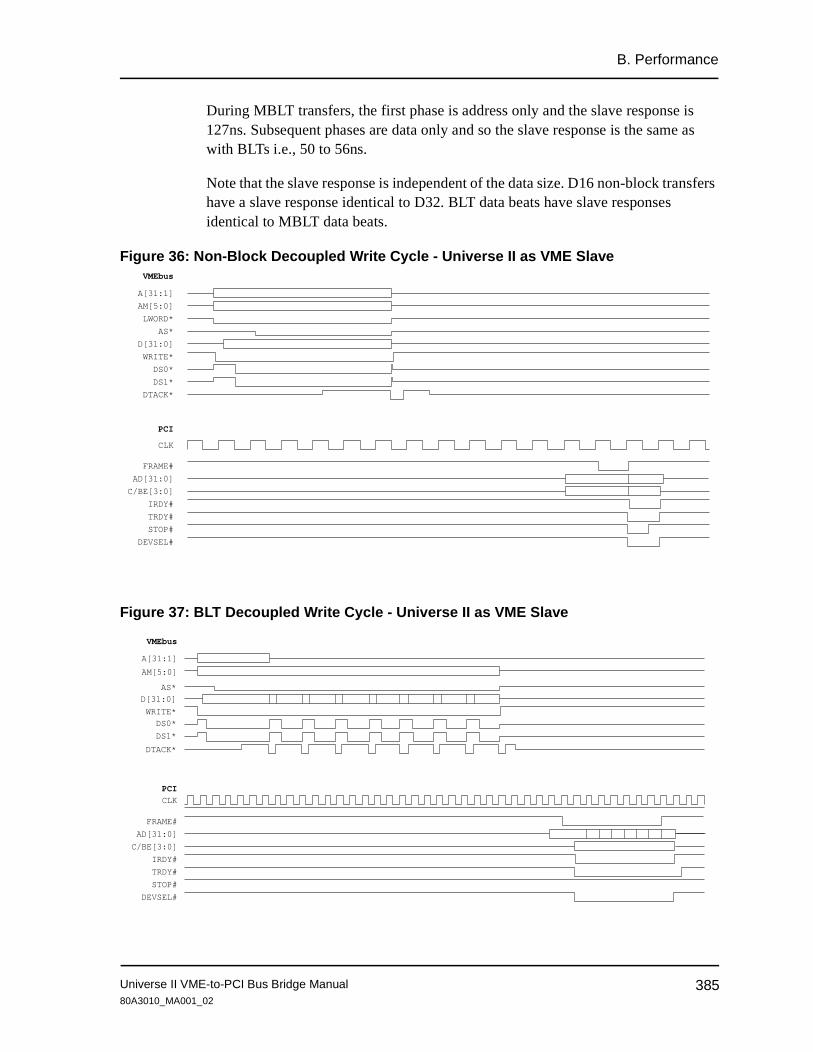
B. Performance
During MBLT transfers, the first phase is address only and the slave response is 127ns. Subsequent phases are data only and so the slave response is the same as with BLTs i.e., 50 to 56ns.
Note that the slave response is independent of the data size. D16 non-block transfers have a slave response identical to D32. BLT data beats have slave responses identical to MBLT data beats.
Figure 36: Non-Block Decoupled Write Cycle - Universe II as VME Slave
Figure 37: BLT Decoupled Write Cycle - Universe II as VME Slave
A[31:1]
AM[5:0]
LWORD*
AS*
D[31:0]
WRITE*
DS0*
DS1*
DTACK*
PCI
VMEbus
CLK
FRAME#
AD[31:0]
C/BE[3:0]
IRDY#
TRDY#
STOP#
DEVSEL#
A[31:1]
AM[5:0]
AS*D[31:0]
WRITE*DS0*
DS1*
DTACK*
PCI
VMEbus
CLK
FRAME#
AD[31:0]
C/BE[3:0]
IRDY#
TRDY#
STOP#
DEVSEL#
Universe II VME-to-PCI Bus Bridge Manual 38580A3010_MA001_02

B. Performance
Figure 38: MBLT Decoupled Write Cycle - Universe II as VME Slave
B.4.1.3 PCI Master PerformanceThe Universe II supports bus parking. If the Universe II requires the PCI bus it will assert REQ_ only if its GNT_ is not currently asserted. When the PCI Master Module is ready to begin a transaction and its GNT_ is asserted, the transfer begins immediately. This eliminates a possible one clock cycle delay before beginning a transaction on the PCI bus which would exist if the Universe II did not implement bus parking. Bus parking is described in Section 3.4.3 of the PCI Specification (Rev. 2.1).
On the PCI bus, the Universe II deliquesce data from the RXFIFO once a complete VME transaction has been enqueued or once sufficient data has been enqueued to form a PCI transaction of length defined by the PABS field.
Since the Universe II does not perform any address phase deletion, non-block transfers are decreed from the RXFIFO as single data beat transactions. Only block transfers result in multi-data beat PCI transactions; typically 8, 16 or 32 data beats. In either case, the Universe II does not insert any wait states as a PCI master. The clock, after the bus has been granted to the Universe II, drives out FRAME_ to generate the address phase. The data phases begin immediately on the next clock. If there is more than one data phase, each phase will immediately follow the acknowledgment of the previous phase.
In each case, because of the lack of any wait states as a PCI master, the Universe II is consuming the minimum possible bandwidth on the PCI bus, and data will be written to the PCI bus at an average sustained rate equal to the rate at which the VME master is capable of writing it.
A[31:1]
AM[5:0]
AS*D[31:0]
WRITE*DS0*
DS1*
DTACK*
PCI
VMEbus
CLK
REQ#
GNT#FRAME#
AD[31:0]
C/BE[3:0]
IRDY#
TRDY#
STOP#
DEVSEL#
Universe II VME-to-PCI Bus Bridge Manual38680A3010_MA001_02

B. Performance
The sustained performance on the PCI bus performing single data beat write transactions to a 32-bit PCI bus is 15 MB/s; double this for a 64-bit bus. When performing 32-byte transactions the sustained performance increases to 106 MB/s; 120 MB/s with 64-byte transactions. Again, these can be doubled for a 64-bit PCI bus. Bear in mind that the PCI bus can only dequeue data as fast as it is being enqueued on the VMEbus. Hence, as the RXFIFO empties, the sustained performance on the PCI will drop down to match the lower performance on the VME side. However, even with the decreased sustained performance, the consumed bandwidth will remain constant (no extra wait states are inserted while the Universe II is master of the PCI bus.)
These numbers assume the PCI bus is granted to the Universe II immediately and that the writes are to a zero-wait state PCI target capable of accepting the full burst length. Figure 29 through Figure 38 show the Universe II responding to non-block, BLT and MBLT write transactions to a 32-bit PCI bus. Even better performance is obtained with PCI bus parking.
B.4.2 Prefetched Read CyclesTo minimize its slave response, the Universe II generates prefetched reads to the PCI bus in response to BLT and MBLT reads coming in from the VMEbus. This option must first be enabled on a per image basis.
When enabled, the Universe II will respond to a block read by performing burst reads on the PCI bus of length defined by the PCI Aligned Burst Size (PABS in the MAST_CTL register). These burst reads continue while the block transfer is still active on the VMEbus (AS* not negated) and there is room in the RDFIFO. If there is insufficient room in the RDFIFO to continue (a common occurrence since the Universe II is capable of fetching data from the PCI bus at a much faster rate than a VME master is capable of receiving it), then pre-fetching stops and only continues once enough room exists in the RDFIFO for another full burst size.
The first data beat of a block transfer must wait for the first data beat to be retrieved from the PCI bus—this is essentially a coupled transfer. See the section on coupled transfers for details on coupled performance. However, once the pre-fetching begins, data is provided by the Universe II in subsequent data beats with a slave response of 57ns. This continues while there is data in the RDFIFO. If the RDFIFO empties because data is being fetched from the PCI bus too slowly, wait states are inserted on the VMEbus awaiting the enqueueing of more data.
Universe II VME-to-PCI Bus Bridge Manual 38780A3010_MA001_02

B. Performance
On the PCI bus, the Universe II fetches data at 89 MB/s with PABS set to 32-byte transactions; 106 MB/s when set to 64-byte transactions. Even better performance is obtained if PABS is set for 128-byte transactions. Once the RDFIFO fills, pre-fetching slows to match the rate at which it is being read by the external VMEbus master. Bandwidth consumption, however, remains constant, only the idle time between transactions increases.
Figure 39: BLT Pre-fetched Read Cycle - Universe II as VME Slave
Group: A
Group: VME
Va[31:0] = 'h zzzzzzzz
vam[5:0] = 'h 3F
Vas = z
Vd[31:0] = 'h zzzzzzzz
vwrite = 1
Vds0 = z
Vds1 = z
Vdtack = z
Group: PCI
pclk = 1
reqnn[0] = 1
gntnn[0] = 1
framenn = 1
ad_low[31:0] = 'h A5A5A5A5
cxbenn_low[3:0] = 'h 5
irdynn = 1
trdynn = 1
stopnn = 1
devselnn = 1
FFF41000
3F 0B 0B 0B * * * * 3F
0* xxxxxxxx 5D1* 5* * * * * *
A5A5A5A5 0004107C
5 0 C
18,345.94 ns16,600.88 17,000 17,500 18,000
Cursor1 = 16,600.88 nsCursor2 = 18,345.94 ns
Universe II VME-to-PCI Bus Bridge Manual38880A3010_MA001_02

B. Performance
B.5 DMA ChannelB.5.1 Relative FIFO sizes
Two fixed “watermarks” in the DMA Channel control the Universe’s II requisition of the PCI bus and VMEbus. The DMAFIFO PCI Watermark is 128 bytes. This means that during reads from the PCI bus, the Universe II will wait for 128 bytes to be free in the DMAFIFO before requesting the PCI bus. For PCI writes, the Universe II waits for 128 bytes of data to be in the FIFO before requesting the PCI bus. The DMAFIFO VMEbus watermark is 64 bytes. This means that during reads from the VMEbus, the Universe II will wait for 64 bytes to be free in the DMAFIFO before requesting the Vmebus. For VMEbus writes, the Universe II waits for 64 bytes of data to be in the FIFO before requesting the VMEbus.
These watermarks have been tailored for the relative speeds of each bus, and provide near optimal use of the DMA channel.
B.5.2 VMEbus Ownership ModesThe DMA has two counters that control its access to the VMEbus: the VON (VMEbus On) counter and the VOFF (VMEbus Off) timer. The VON counter controls the number of bytes that are transferred by the DMA during any VMEbus tenure, while the VOFF timer controls the period before the next request after a VON time-out.
While the bus is more optimally shared between various masters in the system, and average latency drops as the value programmed for the VON counter drops, the sustained performance of the DMA also drops. The DMA is typically limited by its performance on the VMEbus. As this drops off with greater re-arbitration cycles, the average VMEbus throughput will drop. Even if the Universe II is programmed for ROR mode, and no other channels or masters are requesting the bus, there will be a period of time during which the DMA will pause its transfers on the bus, due to the VON counter expiring.
An important point to consider when programming these timers is the more often the DMA relinquishes its ownership of the bus, the more frequently the PCI Slave Channel will have access to the VMEbus. If DMA tenure is too long, the TXFIFO may fill up causing any further accesses to the bus to be retried. In the same fashion, all coupled accesses will be retried while the DMA has tenure on the bus. This can significantly affect transfer latency and should be considered when calculating the overall system latency.
Universe II VME-to-PCI Bus Bridge Manual 38980A3010_MA001_02

B. Performance
B.5.3 VME TransfersOn the VMEbus, the Universe II can perform D08 through D64 transactions in either block or non-block mode. The time to perform a single beat, however, is independent of the bus width being used. Hence, a D08 transaction will transfer data at 25% the rate of a D32, which in turn is half that for D64.
There is a significant difference between the performance for block vs. non-block operations. Because of the extra addressing required for each data transfer in non-block operations, the DMA performance is about half that compared to operating in block mode. Moreover, considering that most VME slaves respond less quickly in non-block mode, the overall performance may drop to one-quarter of that achievable in block mode.
When programmed for Release-When-Done operation, the Universe II will perform an early release of BBSY* when the VON counter reaches its programmed limit. This gives other masters a chance to use the VMEbus (and possibly access the VME Slave Channel), but may decrease performance of the DMA Channel; this factor may also play in favor of the DMA Channel, by pausing the PCI Target Channel’s use of the VMEbus.
B.5.3.1 Read TransfersWhen performing non-block reads on the VMEbus, the Universe II cycle time (AS* to next AS*) is approximately 209ns, which translates to about 20 MB/s when performing D32 transfers. For block transfers the cycle time (DS* to next DS*) falls to about 156ns, or 25 MB/s for D32 transfers. For multiplexed block transfers (MBLTs) the cycle time remains the same, but because the data width doubles, the transfer rate increases to about 50MB/s.
B.5.3.2 Write TransfersNon-block writes to the VMEbus occur at 180ns cycle time (AS* to next AS*), or 23MB/s during D32 transfers. Block writes, however, are significantly faster with a 116ns cycle time (DS* to next DS*), or 36 MB/s. Multiplexed block transfers have slightly longer cycle times at about 112ns (DS* to next DS*), or 62 MB/s with D64 MBLTs.
B.5.4 PCI TransfersAs a master on the PCI bus, the Universe II DMA follows the same general set of rules as the VME Slave channel does: it never inserts any wait states into the transfer (i.e., it never negates IRDY_ until the transaction is complete) and will whenever possible, generate full aligned bursts as set in the PABS field of the MAST_CTL register.
Universe II VME-to-PCI Bus Bridge Manual39080A3010_MA001_02

B. Performance
Between transactions on the PCI bus, the Universe II DMA typically sits idle for 6 clocks. Hence, minimizing the number of idle periods and re-arbitration times by setting PABS to its maximum value of 128 bytes may increase the performance of the DMA on this bus. Higher PABS values imply that the Universe II will hold on to both the PCI bus and the VMEbus for longer periods of time. The reason that PABS also may impact on VMEbus tenure is that (in the case of PCI writes), the DMA FIFO is less likely to fill, and (in the case of PCI reads) the DMA is less likely to go empty. However, given the relative speeds of the buses, and the relative watermarks, the effect of PABS on VMEbus utilization is not as significant as its effects on the PCI bus.
While higher values of PABS increase DMA throughput, they may increase system latency. That is, there will be a longer latency for other PCI transactions, including possible transactions coming through the VME Slave Channel (since the DMA channel will own the PCI bus for longer periods of time). Also, accesses between other PCI peripherals will, on average, have a longer wait before being allowed to perform their transactions. PCI latency must be traded off against possible DMA performance.
Although both read and write transactions occur on the PCI bus with zero wait states, there is a period of six PCI clocks during which the Universe II remains idle before re-requesting the bus for the next transaction. PCI bus parking may be used to eliminate the need for re-arbitration.
With PABS set for 32-byte transactions on a 32-bit PCI bus, this translates to a peak transfer rate of 97 MB/s for reads (including pre-fetching), 98 MB/s for writes, doubling to 194 and 196 for a 64-bit PCI bus. With PABS set for 64-byte transactions, the peak transfer rate increases to 118 MB/s for reads, 125 MB/s for writes on a 32-bit PCI bus—236 MB/s and 250 MB/s respectively for 64-bit PCI buses. The numbers for writes to PCI assume that data are read from VME using BLTs.
Figure 40: PCI Read Transactions During DMA OperationPCI
CLK
REQ#
GNT#
FRAME#
AD[31:0]
C/BE[3:0]
IRDY#
TRDY#
STOP#
DEVSEL#
Universe II VME-to-PCI Bus Bridge Manual 39180A3010_MA001_02

B. Performance
Figure 41: Multiple PCI Read Transactions During DMA Operation
B.6 Universe II Specific RegisterThe Universe II Specific Register, U2SPEC, offset 0x4FC, can be used to improve the performance of the Universe II by reducing the latency of key VMEbus timing elements. This register is present in versions of the Universe device which have a Revision ID of 01or 02 — defined in the PCI_CLASS register, offset 008.
B.6.1 Overview of the U2SPEC RegisterAlthough the VMEbus is asynchronous, there are a number of maximum and minimum timing parameters which must be followed. These requirements are detailed in the VME64 Specification.
In order to qualify as compliant the master, slave and location monitor devices must guarantee they meet these timing parameters independent of their surroundings. They must assume zero latency between themselves and the VMEbus. This, in practice, is never the case. Buffers, transceivers and the backplane itself, all introduce latencies that combine to produce additional system delay. The consequence of such delay is the degradation of overall performance.
The PowerSpan’s U2SPEC register enables users to compensate for the latencies which are inherent to their VMEbus system designs. Through the use of this register, users can reduce the inherent delay associated with five key VMEbus timing parameters.
Use of the U2SPEC register may result in violation of the VME64 Specification.
PCI
CLK
REQ#
GNT#
FRAME#
AD[31:0]
C/BE[3:0]
IRDY#
TRDY#
STOP#
DEVSEL#
Universe II VME-to-PCI Bus Bridge Manual39280A3010_MA001_02

B. Performance
B.6.2 Adjustable VME Timing ParametersB.6.2.1 VME DTACK* Inactive Filter (DTKFLTR)
In order to overcome the DTACK* noise typical of most VME systems, the PowerSpan quadruple samples this signal with the 64 MHz clock. The extra sampling is a precaution that results in decreased performance. Users who believe their systems to have little noise on their DTACK* lines can elect to filter this signal less, and thus increase their Universe II and PowerSpan response time.
B.6.2.2 VME Master Parameter t11 Control (MASt11) According to the VME64 Specification, a VMEbus master must not drive DS0* low until both it and DS1* have been simultaneously high for a minimum of 40 ns. The MASt11 parameter in the U2SPEC register, however, allows DS0* to be driven low in less than 40 ns.
B.6.2.3 VME Master Parameter t27 Control (READt27)During read cycles, the VMEbus master must guarantee the data lines are valid within 25 ns after DTACK* is asserted. The master must not latch the data and terminate the cycle for a minimum of 25 ns after the falling edge of DTACK*.
The READt27 parameter in the U2SPEC register supports faster cycle termination with one of two settings. One setting allows data to be latched and the cycle terminated with an associated delay that is less than 25 ns. The second setting results in no delay in latching and termination.
B.6.2.4 VME Slave Parameter t28 Control (POSt28)According to the VME64 Specification, VMEbus slaves must wait at least 30 ns after the assertion of DS* before driving DTACK* low. When the Universe II or PowerSpan is acting as a VME slave, the POSt28 parameter in the U2SPEC register enables DTACK* to be asserted in less than 30 ns when executing posted writes.
B.6.2.5 VME Slave Parameter t28 Control (PREt28)VMEbus slaves must wait at least 30ns after the assertion of DS* before driving DTACK* low. When the Universe II or PowerSpan is acting as a VME slave in the transaction, PREt28 parameter in the U2SPEC register enables DTACK* to be asserted in less than 30 ns when executing pre-fetched reads.
Universe II VME-to-PCI Bus Bridge Manual 39380A3010_MA001_02
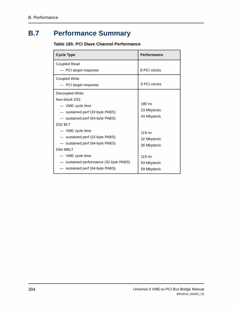
B. Performance
B.7 Performance SummaryTable 165: PCI Slave Channel Performance
Cycle Type Performance
Coupled Read
— PCI target response 8 PCI clocks
Coupled Write
— PCI target response 9 PCI clocks
Decoupled Write:
Non-block D32
— VME cycle time
— sustained perf (32-byte PABS)
— sustained perf (64-byte PABS)
D32 BLT
— VME cycle time
— sustained perf (32-byte PABS)
— sustained perf (64-byte PABS)
D64 MBLT
— VME cycle time
— sustained performance (32-byte PABS)
— sustained perf (64-byte PABS)
180 ns
23 Mbytes/s
43 Mbytes/s
119 ns
32 Mbytes/s
35 Mbytes/s
119 ns
53 Mbytes/s
59 Mbytes/s
Universe II VME-to-PCI Bus Bridge Manual39480A3010_MA001_02

B. Performance
Table 166: VME Slave Channel Performance
Cycle Type
Performance
VME Slave Response (ns)
Coupled Read
— non-block
— D32 BLT
— D64 BLT
301
293
322
Coupled Write
— non-block
— D32 BLT
— D64 BLT
278
264
292
Pre-fetched Read
— VME slave response (1st data beat)
— VME slave response (other data beats)
293
57
Decoupled Write
— non-block slave response
— block slave response (1st data beat)
— block slave response (other data beats)
127
127
50
Table 167: DMA Channel Performance
Cycle TypePerformance Mbytes/s
PCI Reads
— 32-byte PABS
— 64byte PABS
97 (194)a
118 (236)
Universe II VME-to-PCI Bus Bridge Manual 39580A3010_MA001_02

B. Performance
PCI Writes
— 32-byte PABS
— 64byte PABS
98 (196)
125 (250)
VME Reads
— non-block D32
— D32 BLT
— D64 MBLT
18
22
45
VME Writes
— non-block D32
— D32 BLT
— D64 MBLT
22
32
65
a. 64-bit PCI performance in brackets.
Table 167: DMA Channel Performance
Cycle TypePerformance Mbytes/s
Universe II VME-to-PCI Bus Bridge Manual39680A3010_MA001_02

C. Reliability Prediction
This appendix discusses the following topics:
• “Physical characteristics” on page 397
• “Thermal characteristics” on page 397
• “Universe II Ambient Operating Calculations” on page 398
• “Thermal vias” on page 399
C.1 OverviewThis section is designed to help the user to estimate the inherent reliability of the Universe II. The information serves as a guide only; meaningful results will be obtained only through careful consideration of the device, its operating environment, and its application.
C.2 Physical characteristics• CMOS gate array
• 120,000 two-input NAND gate equivalence
• 0.5 µm feature size
• 309 mils x 309 mils scribed die size
C.3 Thermal characteristics• Idle power consumption: 1.50 Watts
• Typical power consumption* (32-bit PCI): 2.00 Watts
Universe II VME-to-PCI Bus Bridge Manual 39780A3010_MA001_02

C. Reliability Prediction
• Maximum power consumption (32-bit PCI): 2.70 Watts
• Typical power consumption (64-bit PCI): 2.20 Watts
• Maximum power consumption (64-bit PCI): 3.20 Watts
Maximum power consumption is worst case consumption when the Universe II is performing DMA reads from the VME bus with alternating worst case data patterns ($FFFF_FFFF, $0000_0000 on consecutive cycles), and 100pF loading on the PCI bus
In the majority of system applications, the Universe II consumes typical values or less. Typical power consumption numbers are based on the Universe II remaining idle 30%-50% of the time, which is significantly less than what is considered likely in most systems. For this reason, it is recommended that typical power consumption numbers be used for power estimation and ambient temperature calculations, as described below.
Reliability calculations of the Universe II design in Motorola’s H4EPlus Gate Array family show that the Failure In Time (FIT) rate is 68 at a junction temperature of 125°C (maximum junction temperature). (Failure in time is the basic reliability rate expressed as failures per billion (1e-9) device hours. Mean Time Between Failures (MTBF) is the reciprocal of FIT. MTBF is the predicted number of device hours before a failure will occur.)
C.4 Universe II Ambient Operating CalculationsThe maximum ambient temperature of the Universe II can be calculated as follows:
Ta ≤ Tj - θja * P
Where,
Ta = Ambient temperature (°C)
Tj = Maximum Universe II Junction Temperature (°C)
θja = Ambient to Junction Thermal Impedance (°C / Watt)
P = Universe II power consumption (Watts)
Universe II VME-to-PCI Bus Bridge Manual39880A3010_MA001_02

C. Reliability Prediction
The ambient to junction thermal impedance (θja) is dependent on the air flow in linear feet per minute over the Universe II. The values for θja over different values of air flow are as follows:
For example, the maximum ambient temperature of the 313 PBGA, 32-bit PCI environment with 100 LFPM blowing past the Universe II is:
Ta ≤ Tj - θja * P
Ta ≤ 125 - 17.0 * 2.70
Ta ≤ 79.1 °C
Hence the maximum rated ambient temperature for the Universe II in this environment is 79.1°C. The thermal impedance can be improved by approximately 10% by adding thermal conductive tape to the top of the packages and through accounting for heat dissipation into the ground planes. This would improve the maximum ambient temperature to 87°C in the above example. Further improvements can be made by adding heat sinks to the PBGA package.
Tj values of Universe II are calculated as follows (Tj = θja * P + Ta)
C.5 Thermal viasThe 313-pin plastic BGA package contains thermal vias which directly pipe heat from the die to the solder balls on the underside of the package. The solder balls use the capabilities of the power and ground planes of the printed circuit board to draw heat out of the package.
Table 168: Ambient to Junction Thermal Impedance
Air Flow (LFPM) 0 100 300
313 PBGA 20.10 17.0 15.1
324 CBGA 17.80 15.4 13.5
Table 169: Maximum Universe II Junction Temperature
Extended (125 °C Ambient)a
a. Tundra Semiconductor recommends that the maximum junction temperature of the Universe II does not exceed 150 °C. This temperature limit can be achieved by using heat dissipation techniques, such as heat sinks and forced airflows.
Industrial (85 °C Ambient) Commercial: (70 °C Ambient)
Tj = 17.0 * 2.70 + 125 C = 170.9 C Tj = 17.0 * 2.70 + 85 C = 130.9 C Tj = 17.0 *2.70 + 70 C = 115.9 C
Universe II VME-to-PCI Bus Bridge Manual 39980A3010_MA001_02

C. Reliability Prediction
Universe II VME-to-PCI Bus Bridge Manual40080A3010_MA001_02

D. Endian Mapping
PowerSpan has Little-endian mapping. Little-endian refers to a method of formatting data where address 0 (or the smallest address referencing the data) points to the least significant byte of the data. Data in a system must be consistent; that is, the system must be entirely big-endian or little-endian.
This appendix discusses the following topics:
• “Little-endian Mode” on page 401
D.1 OverviewThe Universe II always performs Address Invariant translation between the PCI and VMEbus ports. Address Invariant mapping preserves the byte ordering of a data structure in a little-endian memory map and a big-endian memory map.
D.2 Little-endian ModeTable 170 below shows the byte lane swapping and address translation between a 32-bit little-endian PCI bus and the VMEbus for the address invariant translation scheme.
Universe II VME-to-PCI Bus Bridge Manual 40180A3010_MA001_02

D. Endian Mapping
Table 170: Mapping of 32-bit Little-Endian PCI Bus to 32-bit VMEbus
PCI Bus
Byte Lane Mapping
VMEbusByte Enables Address
3 2 1 0 1 0 DS1 DS0 A1 LW
1 1 1 0 0 0 D0-D7 <-> D8-D15 0 1 0 1
1 1 0 1 0 1 D8-D15 <-> D0-D7 1 0 0 1
1 0 1 1 1 0 D16-D23 <-> D8-D15 0 1 1 1
0 1 1 1 1 1 D24-D31 <-> D0-D7 1 0 1 1
1 1 0 0 0 0 D0-D7 <-> D8-D15 0 0 0 1
D8-D15 <-> D0-D7
1 0 0 1 0 1 D8-D15 <-> D16-D23 0 0 1 0
D16-D23 <-> D8-D15
0 0 1 1 1 0 D16-D23 <-> D8-D15 0 0 1 1
D24-D31 <-> D0-D7
1 0 0 0 0 0 D0-D7 <-> D24-D31 1 0 0 0
D8-D15 <-> D16-D23
D16-D23 <-> D8-D15
0 0 0 1 0 1 D8-D15 <-> D16-D23 0 1 0 0
D16-D23 <-> D8-D15
D24-D31 <-> D0-D7
0 0 0 0 0 0 D0-D7 <-> D24-D31 0 0 0 0
D8-D15 <-> D16-D23
D16-D23 <-> D8-D15
D24-D31 <-> D0-D7
Universe II VME-to-PCI Bus Bridge Manual40280A3010_MA001_02

D. Endian Mapping
The unpacking of multiplexed 64-bit data from the VMEbus into two 32-bit quantities on a little-endian PCI bus is outlined in Table 171 below.
Table 171: Mapping of 32-bit Little-Endian PCI Bus to 64-bit VMEbus
Byte Enables Address
PCI to VME Byte Lane Mapping3 2 1 0 2 1 0
First Transfer (D32-D63)
0 0 0 0 0 0 0 D0-D7 <-> A24-A31 (D56-D63)
D8-D15 <-> A16-A23 (D48-D55)
D16-D23 <-> A8-A15 (D40-D47)
D24-D31 <-> LWORD, A1-A7 (D32-D39)
Second Transfer (D0-D31)
0 0 0 0 1 0 0 D0-D7 <-> D24-D31
D8-D15 <-> D16-D23
D16-D23 <-> D8-D15
D24-D31 <-> D0-D7
Universe II VME-to-PCI Bus Bridge Manual 40380A3010_MA001_02

D. Endian Mapping
Universe II VME-to-PCI Bus Bridge Manual40480A3010_MA001_02

E. Typical Applications
This appendix discusses the following topics:
• “VME Interface” on page 405
• “PCI Bus Interface” on page 412
• “Manufacturing Test Pins” on page 414
• “Decoupling VDD and VSS on the Universe II” on page 415
E.1 OverviewBeing a bridge between standard interfaces, the Universe II requires minimal external logic to interface to either the VMEbus or to the PCI bus. In most applications, only transceivers to buffer the Universe II from the VMEbus, plus some reset logic are all that is required. The following information should be used only as a guide in designing the Universe II into a PCI/VME application. Each application will have its own set-up requirements.
E.2 VME InterfaceE.2.1 Transceivers
The Universe II has been designed such that it requires full buffering from VMEbus signals. Necessary drive current to the VMEbus is provided by the transceivers while at the same time isolating the Universe II from potentially noisy VMEbus backplanes. In particular, complete isolation of the Universe II from the VMEbus backplane allows use of ETL transceivers which provide high noise immunity as well as use in live insertion environments. The VME community has recently standardized “VME64 Extensions” (ANSI VITA 1.1) which among other new VME features, facilitates live insertion environments.
Universe II VME-to-PCI Bus Bridge Manual 40580A3010_MA001_02

E. Typical Applications
If neither live insertion nor noise immunity are a concern, those buffers that provide input only (U15 and U17 in Figure 42) may be omitted. The daisy chain input signals, BGIN[3:0] and IACKIN, have Schmitt trigger inputs, which should rectify any minor noise on these signals. If considerable noise is expected, the designer may wish to put external filters on these signals. Bear in mind that any filtering done on these signals will detrimentally affect the propagation of bus grants down the daisy chain. Only extremely noisy systems or poorly designed backplanes should require these filters.
Figure 42 shows one example of how to connect the Universe II to the VMEbus. The transceivers in this example were chosen to meet the following criteria:
• provide sufficient drive strength as required by the VME specification
• meet Universe II skew requirements, and
• minimize part counts.
U15 and U17 in Figure 42 are optional devices. They will provide better noise immunity.
Universe II VME-to-PCI Bus Bridge Manual40680A3010_MA001_02

E. Typical Applications
Figure 42: Universe II Connections to the VMEbus Through TTL Buffers
G
DIR
A0
A1
A2
A3
A4
A5
A6
A7
B0
B1
B2
B3
B4
B5
B6
B7
G
DIR
A0
A1
A2
A3
A4
A5
A6
A7
B0
B1
B2
B3
B4
B5
B6
B7
G
DIR
A0
A1
A2
A3
A4
A5
A6
A7
B0
B1
B2
B3
B4
B5
B6B7
G
DIR
A0
A1
A2
A3
A4
A5
A6
A7
B0
B1
B2
B3
B4
B5
B6
B7
G
DIR
A3
A4
A5
A6
A7
B0
B1
B2
B3
B4
B5
B6
B7
G
DIR
A0
A1
A2
A3
A4
A5
A6
A7
B0
B1
B2
B3
B4
B5
B6
B7
G
DIR
A0
A1
A2
A3
A4
A5
A6
A7
B0
B1
B2
B3
B4
B5
B6
B7
G
DIR
A0
A1
A2
A3
A4
A5
A6
A7
B0
B1
B2
B3
B4
B5
B6
B7
G
DIR
A0
A1
A2
G
DIR
A0
A1
A2
A3
A4
A5
B0
B1
B2
B3
B4
B5
B6
B7
U10:A
U11:
U10:B
U11:B
U11:C
U10:D
U11:D
U12:A
U12:B
U13:A
U11:A
Universe VMEbusA[31:1],LWORD*
D[31:0]
AM[5:0]
AS*
DS[1:0]*
DTACK*
SYSCLK
BCLR*
VSCON_DIR
VBCLR_
SYSCLK_
VSLAVE_DIR
VDTACK_
VDS_DIR
VDS1_
VDS0_
VAS_DIR
VAS_
VAM[5:0] VWRITE_
VIACK_
WRITE*IACK*
VAM_DIR
VD[31:0]
VA[31:1],LWORD*
VD_DIR
VA_DIRVOE_
U1 U2 U3 U4
U5 U6 U7 U8
U9
U10:C
Universe II VME-to-PCI Bus Bridge Manual 40780A3010_MA001_02

E. Typical Applications
Figure 43: Universe II Connections to the VMEbus Through TTL Buffers
Vcc
VXBBSY
VRBBSY_
VXSYSFAIL
VRSYSFAIL_
VXSYSRST
VRSYSRST_
VXBERR
VRBERR_
VXBR[3:0]
VRBR[3:0]_
VXIRQ[7:1]
VRIRQ[7:1]_7
7
4
4
U14:A
U15:A
VRACFAIL_
U15:C
U14:C
U14:D
U15:D
U14:E
U15:E
U14:F-H, U16:A-D
U15:F-H, U17:A-D
U16:E-H
U17:E-H
VIACKIN_
VIACKOUT_
VBGIN[3:0]_
VBGOUT[3:0]_ 4
4
U15:B
BBSY*
ACFAIL*
SYSFAIL*
SYSRST*
BERR*
IRQ[7:1]*
BR[3:0]*
BG[3:0]IN*
BG[3:0]OUT*
IACKIN*
IACKOUT*
Universe VMEbus
U1-U9U10, U12U11, U13U15, U17
'245'126'125'241
Note: U15 & U17 are optional
Universe II VME-to-PCI Bus Bridge Manual40880A3010_MA001_02

E. Typical Applications
The Universe II, with the addition of external transceivers, is designed to meet the timing requirements of the VME specification. Refer to the VME64 specification (ANSI VITA 1.0) for details on the VME timing. In order to meet the requirements outlined in this specification, the external transceivers must meet certain characteristics as outlined in Table 173.
Table 172: VMEbus Signal Drive Strength Requirements
VME bus Signal Required Drive Strength
A[31:1], D[31:0], AM[5:0], IACK*, LWORD*, WRITE*, DTACK* IOL ≥ 48mA
IOH ≥ 3mA
AS*, DS[1:0]*, IOL ≥ 64mA
IOH ≥ 3mA
SYSCLK* IOL ≥ 64mA
IOH ≥ 3mA
BR[3:0]*, BSY*, IRQ[7:0]*, BERR*, SYSFAIL*, SYSRESET* IOL≥ 48mA
Table 173: VMEbus Transceiver Requirements
Parameter From To Timing
(Input) (Output) Min Max
VA, VD, VAM, VIACK, VLWORD, VWRITE, VAS, VDSx, VDTACKa
a. There are no limits on propagation delay or skew on the remaining buffered VME signals: VSYSCLK, VBCLR, VXBBSY, VRBBSY, VRACFAIL, VXSYSFAIL, VRSYSFAIL, VXSYSRST, VRSYSRST, VXBERR, VRBERR, VXIRQ, VRIRQ, VXBR, VRBR.
skew (pkg to pkg) A B 8 ns
skew (pkg to pkg) B A 4 ns
tProp DIR A 1 ns 5ns
tProp DIR B 2 ns 10ns
Cin A 25 pf
Universe II VME-to-PCI Bus Bridge Manual 40980A3010_MA001_02

E. Typical Applications
F Series transceivers meet the requirements specified in Table 172 and Table 173. A faster family such as ABT, may also be used. Care should be taken in the choice of transceivers to avoid ground bounces and also to minimize crosstalk incurred during switching. To limit the effects of crosstalk, the amount of routing under these transceivers must be kept to a minimum. Daisy chain signals can be especially susceptible to crosstalk.
Should the designer wish to put any further circuitry between the Universe II and the VMEbus, that circuitry must meet the same timing requirements as the transceivers in order for the combined circuit to remain compliant with the VME64 specification.
E.2.1.1 Pull-down resistorsThe Universe II has internal pull-down resistors which are used for its default power-up option state. (Note that REQ64_ has an internal pull-up.) These internal pull-down resistors, ranging from 25kΩ-500kΩ, are designed to sink between 10µA-200µA. F-series buffers, however, can source up to 650 µA of current (worst case). This sourced current has the ability to override the internal power up resistors on the Universe II. This may cause the Universe II to incorrectly sample a logic “1” on the pins. To counteract this potential problem, assuming a worst case scenario of a 650 µA current, Tundra recommends connecting a 1K resistor to ground, in parallel, with the internal pull-down resistor.
Tundra recommends that any pins controlling the power-up options which are critical to the application at power-up be connected to ground with a pull-down resistor as described above. If these options are not critical and if it is possible to reprogram these options after reset, additional resistors need not be added.
E.2.2 Direction controlWhen the Universe II is driving VMEbus lines, it drives the direction control signals high (i.e., VA_DIR, VAM_DIR, VAS_DIR, VD_DIR, VDS_DIR, VSLAVE_DIR, and VSCON_DIR). When the VMEbus is driving the Universe II, these signals are driven low. The control signals in the Universe II do not all have the same functionality. Since the Universe II implements early bus release, VAS_DIR must be a separate control signal.
Contention between the Universe II and the VME buffers is handled since the Universe II tristates its outputs one 64MHz clock period before the buffer direction control is faced inwards.
Universe II VME-to-PCI Bus Bridge Manual41080A3010_MA001_02

E. Typical Applications
E.2.3 Power-up OptionsPower-up options for the automatic configuration of slave images and other Universe II features are provided through the state of the VME address and data pins, VA[31:1] and VD[31:27]. All of these signals are provided with internal pull-downs to bias these signals to their default conditions. Should values other than the defaults be required here, either pull-ups or active circuitry may be applied to these signals to provide alternate configurations.
Power-up options are described in “Resets, Clocks and Power-up Options” on page 153.
Since the power-up configurations lie on pins that may be driven by the Universe II or by the VME transceivers, care must be taken to ensure that there is no conflict. During any reset event, the Universe II does not drive the VA or VD signals. As well, during any VMEbus reset (SYSRST*) and for several CLK64 periods after, the Universe II negates VOE_ to tri-state the transceivers. During the period that these signals are tri-stated, the power-up options are loaded with their values latched on the rising edge of PWRRST_.
Configuration of power-up options is most easily accomplished through passive 10k pull-up resistors on the appropriate VA and VD pins. The configurations may be made user-configurable through jumpers or switches as shown in Figure 44
Figure 44: Power-up Configuration Using Passive Pull-ups
Alternatively, an active circuit may be designed which drives the VA and VD pins with pre-set (or pre-programmed) values. This sort of circuit would be of value when power-up configurations such as the register access slave image are stored in an external programmable register. To implement this circuit, the VOE_ output from the Universe II must be monitored. When the Universe II negates this signal, the appropriate VA and VD signals may be driven and upon re-assertion the drive must be removed. To avoid conflict with the transceivers, logic must be designed such that the enabling of the transceivers does not occur until some point after the configuration options have been removed from the VD and VA signals. Figure 45 shows one such implementation. The delay for enabling of the VMEbus transceivers could be implemented though clocked latches.
Power-up Pins
Universe II VDD
Universe II VME-to-PCI Bus Bridge Manual 41180A3010_MA001_02

E. Typical Applications
Figure 45: Power-up Configuration Using Active Circuitry
E.2.3.1 Auto-Syscon and PCI Bus Width Power-up OptionsThe VME64 specification provides for automatic enabling of the system controller in a VME system through monitoring of the BGIN3* signal. If at the end of SYSRST* this pin is low, then the system controller is enabled; otherwise it is disabled. The Universe II provides an internal pull-down resistor for this function. If it is in slot one, this pin will be sampled low. If not in slot one, then it will be driven high by the previous board in the system and system controller functions will be disabled. No external logic is required to implement this feature.
E.3 PCI Bus InterfaceThe Universe II provides a fully standard PCI bus interface compliant for both 32-bit and 64-bit designs. No external transceivers or glue logic is required in interfacing the Universe II to any other PCI compliant devices. All signals may be routed directly to those devices.
The Universe II’s PCI interface can be used as a 32-bit bus or 64-bit bus. If used as a 32-bit interface, the 64-bit pins, AD[32:63] and ACK64_ are left unterminated. On a 32-bit PCI bus, the Universe II drives all its 64-bit extension bi-direct signals (C/BE[7:4]_, AD[63:32], REQ64_, PAR64 and ACK64_) at all times to unknown values. Independent of the setting of the LD64EN bit, the Universe II will never attempt a 64-bit cycle on the PCI bus if it is powered up as 32-bit.
REQ64_ must be pulled-down (with a 4.7kΩ resistor) at reset for 64-bit PCI (see “PCI Bus Width” on page 164). There is an internal pull-up on this pin which causes the Universe II to default to 32-bit PCI. This power-up option provides the necessary information to the Universe II so that these unused pins may be left unterminated.
Power-up Pins
Universe IIExternal Register
OE_VOE_ Tranceivers VM
EbusOE_Delay
Universe II VME-to-PCI Bus Bridge Manual41280A3010_MA001_02

E. Typical Applications
E.3.1 ResetsThe Universe II provides several reset input and outputs which are asserted under various conditions. These can be grouped into three types as shown in Table 174.
E.3.1.1 VMEbus ResetsThe VMEbus resets are connected to the VMEbus as indicated in Figure 42 on page 407 through external buffers.
E.3.1.2 PCI bus ResetsUse of the PCI bus resets will be application dependent. The RST_ input to the Universe II should typically be tied in some fashion to the PCI bus reset signal of the same name. This will ensure that all Universe II PCI related functions are reset together with the PCI bus.
The LRST_ pin is a totem-pole output which is asserted due to any of the following initiators:
• PWRRST_,
• VRSYSRST_,
• local software reset (in the MISC_CTL register), or
• VME CSR reset (in the VCSR_SET register).
The designer may wish to disallow the Universe II from resetting the PCI bus in which case this output may be left unconnected. Otherwise LRST_ should be grouped with other PCI reset generators to assert the RST_ signal such that:
RST_ = LRST_ & reset_source1 & reset_source2 &...
If the Universe II is the only initiator of PCI reset, LRST_ may be directly connected to RST_.
Table 174: Reset Signals
Group Signal Name Direction
VMEbus VXSYSRST output
VRSYSRST_ input
PCI bus LRST_ output
RST_ input
VME_RESET_ input
Power-up PWRRST_ input
Universe II VME-to-PCI Bus Bridge Manual 41380A3010_MA001_02

E. Typical Applications
Assertion of VME_RESET causes the Universe II to assert VXSYSRST.
To reset the VMEbus through this signal it is recommended that it be asserted for several clock cycles, until the Universe II asserts RST_, and then released. This ensures a break is made in the feedback path.
E.3.1.3 Power-Up ResetThe PWRRST_ input is used to provide reset to the Universe II until the power supply has reached a stable level. It should be held asserted for 100 milliseconds after power is stable. Typically this can be achieved through a resistor/capacitor combination although more accurate solutions using under voltage sensing circuits (e.g. MC34064) are often implemented. The power-up options are latched on the rising edge of PWRRST_.
E.3.1.4 JTAG ResetThe JTAG reset, TRST_, should be tied into the master system JTAG controller. It resets the Universe II internal JTAG controller. If JTAG is not being used, this pin should be tied to ground.
E.3.2 Local InterruptsThe Universe II provides eight local bus interrupts, only one of which has drive strength that is fully PCI compliant. If any of the other seven interrupts are to be used as interrupt outputs to the local bus (all eight may be defined as either input or output), an analysis must be done on the design to determine whether the 4 mA of drive that the Universe II provides on these lines is sufficient for the design. If more drive is required, the lines may simply be buffered.
All Universe II interrupts are initially defined as inputs. To prevent excess power dissipation, any interrupts defined as inputs should always be driven to either high or low. Pull-ups should be used for this purpose rather than direct drive since a mis-programming of the interrupt registers may cause the local interrupts to be configured as outputs and potentially damage the device.
E.4 Manufacturing Test PinsThe Universe II has several signals used for manufacturing test purposes. They are listed in Table 25 on page 165, along with the source to which they should be tied.
This signal must not by tied to the PCI RST_ signal unless the Universe II LRST_ output will not generate a PCI bus reset. Connecting both LRST_ and VME_RESET_ to RST_ will cause a feedback loop on the reset circuitry forcing the entire system into a endless reset.
Universe II VME-to-PCI Bus Bridge Manual41480A3010_MA001_02

E. Typical Applications
E.5 Decoupling VDD and VSS on the Universe IIThis section is intended to be a guide for decoupling the power and ground pins on the Universe II. A separate analog power and ground plane is not required to provide power to the analog portion of the Universe II. However, to ensure a jitter free PLL operation, the analog AVDD and AVSS pins must be noise free. The following are recommended solutions for noise free PLL operation. The design could implement one of these solutins, but not both.
The Analog Isolation Scheme consists of the following:
• a 0.1µF capacitor between the AVDD and AVSS pins, and
• corresponding inductors between the pins and the board power and ground planes (See Figure 46). These inductors are not necessary, but they are recommended.
Figure 46: Analog Isolation Scheme
The Noise Filter Scheme filters out the noise using two capacitors to filter high and low frequencies (See Figure 47).
Figure 47: Noise Filter Scheme
Board VDD
Board VSS
AVDD
AVSS
1.5 - 220 µH
1.5 - 220 µH
0.1 µF
AVDD
AVSS
0.01 µF
Board VSS
Board VDD
10-38 †
(Low Freq. Bias)
22 µF(High Freq. Bias)
Universe II VME-to-PCI Bus Bridge Manual 41580A3010_MA001_02

E. Typical Applications
For both schemes, it is recommended that the components involved be tied as close as possible to the associated analog pins.
In addition to the decoupling schemes shown above, it is recommended that 0.1µF bypass capacitors should be tied between every three pairs of VDD pins and the board ground plane. These bypass capacitors should also be tied as close as possible to the package.
Universe II VME-to-PCI Bus Bridge Manual41680A3010_MA001_02

F. Ordering Information
This appendix discusses Universe II’s ordering information.
F.1 Ordering InformationTundra Semiconductor Corporation products are designated by a product code. When ordering, refer to products by their full code. Table 175 below details the available part numbers.
Table 175: Standard Ordering Information
Part Numbera
a. The x in the product code means the device number is dependent on if the Universe IIB or the Universe IID is ordered. The Universe IID is recommended for all new designs. For more information about the two devices, refer to the Universe IID and the Universe IIB Differences Summary document on the Tundra website at www.tundra.com.
PCI Frequency Voltage Temperature Package
CA91C142x-33CE 33 MHz 5 V 0° to 70°C PBGA (Plastic)
CA91C142x-33IE 33 MHz 5 V -40° to 85°C PBGA (Plastic)
CA91C142x-25EE 25 MHz 5 V -55° to 125°C PBGA (Plastic)
CA91C142x-33CB 33 MHz 5 V 0° to 70°C DBGA (Ceramic)
CA91C142x-33IB 33 MHz 5 V -40° to 85°C DBGA (Ceramic)
CA91C142x-25EB 25 MHz 5 V -55° to 125°C DBGA (Ceramic)
Universe II VME-to-PCI Bus Bridge Manual 41780A3010_MA001_02

F. Ordering Information
Universe II VME-to-PCI Bus Bridge Manual41880A3010_MA001_02

IndexAAbsolute Maximum Ratings 188ACFAIL*
interrupt source 131interrupts 129
ACK64_ 49, 67, 73, 87, 164, 174, 176, 412Special Cycle Generator 78
AD 174and Configuration Cycles 52, 54parity checking 68Special PCI target image 90Target-Disconnects 81
Address Translation 401PCI to VME 89VME to PCI 86
Addressing CapabilitiesPCI Master Interface 69VMEbus Master Interface 39
ADOH Cycles 49, 78, 80DMA Channel 126generating 80Target-Retry 96
AS* 50Auto Slot ID
proprietary method 57VME64 specified 56
BBBSY* 37, 38
ADOH cycles 50coupled-cycles 76DMA VMEbus ownership 110
BCLR* 39BERR 42BERR* 42, 45, 71
coupled cycles 148BG3IN* 161
and First Slot Detector 55BGIN 406BGIN3* 412
Universe II VME-to-PCI Bus Bridge Manual80A3010_MA001_02
BI-Mode 60BR3-0* 37Bus Errors
DMA controller 112, 126IACK cycle 137parity 68RXFIFO posted writes 47TXFIFO posted writes 82
Bus Ownership 121Bus Parking 65Byte Enables 402Byte Lane Mapping 402Byte Ordering 401
CC/BE# 164C/BE_ 66, 68, 72, 150, 174CLK64 59, 156, 167, 170Configuration Cycles 52, 67, 70, 93, 94, 95, 104contact information 5Coupled Request Timer 38Coupled Transactions
error handling 148PCI Target Channel 75VMEbus Slave Channel 44
Coupled Wait Phase 76Coupled Window Timer 38, 76customer support information 5Cycle Terminations
PCI Master Interface 71PCI Target Channel 81VMEbus Master Interface 42VMEbus Slave Channel 45, 47
DD_LLUE Register
UPDATE bit 120D32 46, 107, 108Data Transfer
PCI Master Interface 70PCI Target Channel 73VMEbus Master Interface 41VMEbus Slave Channel 44, 45, 47, 50
419

Index
Data Width 108DC Current Drain 188DCPP Register
DCPP field 109DCTL Register 263
L2V bit 104LD64EN bit 109PGM field 105SUPER field 105VAS field 105VCT bit 108VDW bit 108
design support tools (DST) 5DEVSEL# 151DEVSEL_ 67, 72, 87, 174DGCS Register
ACT bit 107, 110, 114, 119, 126CHAIN bit 108DONE bit 110, 112, 114, 115, 120, 121, 126GO bit 109, 110, 112, 114, 115, 118, 119, 121,
126HALT bit 112, 119, 126INT_DONE bit 143INT_HALT bit 143INT_LERR bit 112, 114, 117, 125, 127, 143INT_M_ERR bit 125, 143INT_STOP bit 112, 114, 117, 125, 143INT_VERR bit 112, 114, 117, 125, 127, 143LERR bit 110, 112, 114, 126P_ERR bit 109, 110, 112, 114, 126STOP bit 107, 110, 111, 112, 114, 115, 119, 126STOP_REQ bit 111, 114, 115, 119VERR bit 114, 126VOFF field 111, 114, 117, 124VON field 110, 111, 114, 117, 123, 124
Direction Control 410DLA Register 104DMA Channel
PCI requests 69PCI to VME transfers 121VME tot PCI transfers 123VMEbus release 38VMEbus requests 36
DMA Completion 111DMA Controller
defined 34direct mode operation 112error handling 126, 150FIFO operation and bus ownership 121interrupts 125linked-list operation 115
DMA Interrupts 125
420
DMAFIFO 34packing 122, 123PCI bus watermark 124VMEbus watermark 124
document conventions 22document feedback 6document ordering 6DST (design support tools) 5DTACK 42DTACK* 43, 48, 96
Location Monitors 52RXFIFO 46
DTBC RegisterDTBC field 105
DVA Register 104DY4 Systems 56
Eemail 6Endian Modes 401ENID 174Error Handling
coupled transactions 148DMA controller 150parity 150posted writes 148prefetched reads 150
FFAQ support database 5FIFOs
DMAFIFO 122RDFIFO 48RXFIFO 45TXFIFO 77
First Slot Detector 55FIT rate 398FRAME_ 49, 65, 67, 72, 75, 81, 82, 174
GGNT# 386GNT_ 65, 174
HHigh Impedance Mode 166
IIACK 148IACK* 43, 55
error logging 148IACKIN 406IACKIN* 58
Universe II VME-to-PCI Bus Bridge Manual80A3010_MA001_02

Index
SYSCON 55IACKOUT* 58IDSEL 67, 94, 175Input Voltage 188Interrupt Acknowledge Cycles
auto-ID 57bus errors 137STATUS/ID 137
Interrupt ChannelVMEbus requests 36
Interrupt GenerationPCI bus 131VMEbus 133
Interrupt Handlinginternal sources 138PCI bus 136VMEbus 136
Interrupterdefined 33
IRDY_ 67, 82, 175IRQ* 129, 133
interrupt source 131IRQ2*
Auto Slot ID 56
JJTAG 167, 414
LL_CMDERR Register
CMDERR field 47, 71L_STAT bit 47, 71M_ERR bit 47, 71
LAERR RegisterLAERR field 47
LCLK 67, 167, 175LERR 71, 148Linked-List Operation of DMA 115LINT_ 131, 137, 138, 143, 175LINT_EN Register
ACFAIL bit 132, 133DMA bit 132interrupt sources 131LERR bit 71, 132LMn bit 132MBOXn bit 132SW_IACK bit 132, 141, 143SW_INT bit 132, 142SYSFAIL bit 132, 133VERR bit 43, 82, 132VIR1x bits 132VMEbus interrupt inputs 136
Universe II VME-to-PCI Bus Bridge Manual80A3010_MA001_02
VOWN bit 132LINT_MAP0 Register
interrupt sources 131VERR field 132VIRQ7-1 fields 132, 137, 138VMEbus interrupt handling 132, 137VMEbus interrupt inputs 132VMEbus ownership bit 132VOWN field 132
LINT_MAP1 RegisterACFAIL field 132DMA field 132interrupt sources 131LERR field 132SW_IACK field 132, 143SW_INT field 132SYSFAIL field 132
LINT_MAP2 Register 131LM3-0 fields 144MBOX3-0 fields 144
LINT_STAT Register 149ACFAIL bit 132DMA bit 132interrupt sources 131LERR bit 132LMx bit 144MBOXn bit 132, 144Software interrupts 142SW_INT bit 142SYSFAIL bit 132VERR bit 132VMEbus interrupt handling 137VMEbus interrupt inputs 132VOWN bit 132
Little-Endian Mode 401LM_BS Register 51, 144LM_CTL Register 336
EN bit 51SUPER field 51VAS field 51
LMISC RegisterCWT field 76
Location Monitors 51–52and interrupts 51interrupts 51, 144
LOCK# 86LOCK_ 50, 80, 175Locks
VMEbus Slave Channel 50LRST# 154, 155, 156, 157, 158, 159LRST_ 175, 413LSI2_BD Register 226
421

Index
LSI2_CTL Register 223LSI4_BD Register 246LSI4_BS Register 245LSI4_CTL Register 243LSI4_TO Register 247LSI5_BD Register 251LSI5_BS Register 250LSI5_CTL Register 248LSI5_TO Register 252LSI6_BD Register 256LSI6_BS Register 255LSI6_CTL Register 253LSI6_TO Register 257LSI7_BD Register 261LSI7_BS Register 260LSI7_CTL Register 258LSI7_TO Register 262LSIn_BD Registers
BD field 87Power-up options 160
LSIn_BS RegistersBS field 87Power-up options 160
LSIn_CTL RegistersEN bit 88LAS field 87PGM field 88Power-up options 160PWEN bit 76, 88SUPER field 88VAS field 88VCT field 88VDW field 88
LSIn_TO RegistersTO field 88
MMailbox Registers 101
Interrupts 133mailing address 6MAST_CTL Register 305
BUS_NO field 52, 53, 54MAXRTRY field 71PABS field 46, 48, 49, 70, 150PWON field 38, 42VOWN bit 36, 38, 80, 81, 143VOWN_ACK 80VOWN_ACK bit 36, 81VREL bit 37, 81VRL field 37VRM field 37
Master-Abort
422
defined 67MBOX0 Register 299MBOXn Registers 101, 144MISC_CTL Register 308
AUTOID bit 56BI bit 61, 160ENGBI bit 61SW_LRST bit 155, 157SW_SYSRST bit 157SYSCON bit 55, 58, 160V64AUTO bit 160VARB bit 59VARBTO field 59VBTO field 60
MISC_STAT RegisterDY4AUTO bit 160DY4AUTOID field 58DY4DONE bit 58LCLSIZE bit 160MYBBSY bit 37TXFE bit 38
Monarch 56MTBF 398
NNAND Tree Simulation 166Noise Filter 415Normal Mode 166
OOrdering Information 417ordering information 417
PPAR 68, 72, 150, 175PAR64 68, 72, 150, 175Parity
error handling 150PCI Master Interface 72
Parity CheckingUniverse capability 68
PBGA 399PCI Aligned Burst Size (PABS) 48, 49, 70, 122, 150PCI Cycle Types
Universe II capability 69PCI Interface
32-bit versus 64-bit 64cycle types 66defined 33Universe II as master 68Universe II as slave 72
PCI Master Interface
Universe II VME-to-PCI Bus Bridge Manual80A3010_MA001_02

Index
cycle terminations 71data transfer 70parity 72
PCI RequestsDMA Channel 69VME Slave Channel 68
PCI Slave Imagesdefined 87
PCI Target ChannelADOH cycles 80coupled transactions 75cycle terminations 81data transfer 73posted writes 76read-modify-writes 79TXFIFO 77VMEbus release 38VMEbus reqests 36
PCI Target ImagePower-up Option 160
PCI Terminationsdefined 67
PCI_BS0 Register 209SPACE bit 160
PCI_BS1 Register 210SPACE bit 160
PCI_BSn RegisterBS field 95SPACE bit 96
PCI_BSn RegistersBS field 95SPACE bit 95
PCI_CSR RegisterBM bit 44, 50, 85, 109, 112
power-up option 160D_PE bit 72, 150DEVSEL field 72DP_D bit 72PERESP bit 72, 150R_MA bit 45, 71R_TA bit 45, 71S_SERR bit 73S_TA bit 82SERR_EN bit 73, 150
PERR# 150, 151PERR_ 72, 150, 175pinout 169PLL 415PLL_TESTOUT 167, 176PLL_TESTSEL 166, 176Posted Writes
error handling 148
Universe II VME-to-PCI Bus Bridge Manual80A3010_MA001_02
errors 47PCI Target Channel 76VMEbus Slave Channel 45
power consumption 398Power Dissipation 188Power-up
register access 55Power-up Options 161, 411
auto-ID 162BI-mode 163PCI bus width 164PCI CSR image space 164PCI slave image 163SYSFAIL assertion 163VME CR/CSR slave image 162VME register access slave image 161
Prefetched Readserror handling 150VMEbus Slave Channel 47
Product Code 417Pull-down resistors 410PWON 379PWRRST# 154, 156, 157, 158, 159, 161, 165, 166PWRRST_ 176, 411, 413, 414
RRDFIFO 32, 48
size 48Read-Modify-Writes
PCI Target Channel 79VMEbus Slave Channel 50
Register Accessat power-up 55configuration space 94CR/CSR access 98from VMEbus 97I/O space 95memory space 95VMEbus register access image 97
Register Map 192Registers ??–102related documentation 25Reliability 397, 398REQ_ 65, 67, 176, 386REQ64# 160, 161, 164REQ64_ 49, 64, 67, 73, 87, 176, 412Request Modes 37Resets 154RETRY* 32, 33, 42RST# 157RST_ 154, 176, 413, 414
BI-MODE 61
423

Index
RXFIFO 45
Ssales support 5SCV64 56SCYC_ADDR Register 234
ADDR field 78SCYC_CMP Register
CMP field 78SCYC_CTL Register
SCYC field 78, 79SCYC_EN Register
EN field 78SCYC_SWP Register
SWP field 78SDONE 64SEMA0 Register 102SEMA1 Register 102SEMAn Register 102Semaphores 102, 120SERR# 150, 151SERR_ 68, 72, 73, 176SLSI Register
BS field 90EN bit 91LAS field 90PGM field 91PWEN bit 91SUPER field 91VDW field 91
Special Cycle Generator 33, 78–81semaphores 102
Special PCI Slave Imagedefined 90
STATID Register 57, 134STATID field 135
STATUS/IDprovided by Universe II 135
STOP_ 67, 68, 82, 176Storage Temperature 188support information 5SYSCON 167SYSFAIL* 145, 163
and auto ID cycle 56Auto ID cycle 56Auto Slot ID 56interrupt source 131interrupts 129
SYSRST* 56, 157, 161, 163, 411, 412Auto ID cycle 56BI-Mode 61
424
TTarget-Abort
defined 68Target-Disconnect
defined 67Target-Retry
defined 68TCK 167, 176TDI 167, 176TDO 167, 176technical support 6Thermal vias 399Time-Outs
VMEbus 60VMEbus arbiter 59
TMODE 166, 167, 177TMS 167, 177TRDY_ 67, 82, 177TRST# 154, 167TRST_ 177TXFIFO 77
UUSER_AM Register 89
USER1AM, USER2AM fields 41
VV_AMERR Register 148
AMERR field 43, 82IACK bit 43, 137M_ERR bit 43, 82V_STAT bit 43, 82
VA 170, 410and Configuration Cycles 53Configuration Cycles 52Location Monitor 144power-up options 160
VA_DIR 170, 410VAERR Register
VAERR field 43, 82VAM 170VAM_DIR 170, 410VAS_ 170VAS_DIR 170, 410VBCLR_ 59, 170VBGI_ 171VBGIN 160VBGO_ 59, 171VCOCTL 165, 167, 177VCSR_BS Register
BS field 98VCSR_CLR Register 159
Universe II VME-to-PCI Bus Bridge Manual80A3010_MA001_02

Index
FAIL bit 159RESET bit 156SYSFAIL bit 57, 156, 159, 160
VCSR_CTL RegisterEN bit 98LAS field 99, 160
VCSR_SET RegisterFAIL bit 159SYSFAIL bit 57, 159, 160
VCSR_TO RegisterTO field 99, 160
VD 171power-up options 160pull-ups 164
VD_DIR 171, 410VDS_ 171VDS_DIR 171, 410VDTACK_ 171VERR 71, 138, 148VIACK_ 171VIACKO_ 172VINT_EN Register
DMA bit 134interrupt sources 134LERR bit 47, 71, 134MBOX3-0 bits 134PCI interrupt inputs 136SW_INT bit 134, 141SW_INT7-1 bits 134, 141, 160VERR bit 43, 82, 134
VINT_MAP0 Register 134VINT_MAP1 Register 134
DMA field 134interrupt sources 134LERR field 134SW_INT bit 160SW_INT field 134, 141VERR field 134
VINT_MAP2 Register 134MBOX3-0 fields 144
VINT_STAT Register 134, 135, 136, 149DMA bit 125, 134IACK cycle error 138interrupt sources 134LERR bit 134, 138LINT7-0 bitS 134LINT7-0 bits 144MBOX3-0 bitS 134MBOX3-0 bits 144PCI interrupt inputs 136SW_INT bit 134, 141, 160SW_INT7-1 bits 134
Universe II VME-to-PCI Bus Bridge Manual80A3010_MA001_02
VERR bit 134, 138VMEbus interrupt handling 137
VLWORD_ 172VME_RESET 414VME_RESET# 154, 157, 159VME_RESET_ 177, 413, 414VMEbus Arbitration 59
arbiter time-out 59priority mode 59round robin 59
VMEbus InterfaceBI-mode 60configuration 54CR/CSR access 98defined 32first slot detector 55requester 35system clock 59system controller 58Universe as master 39Universe as slave 43VMEbus release 37VMEbus time-out 60
VMEbus Master Interfaceaddressing capabilities 39cycle terminations 42data transfer 41
VMEbus Register Access Image 97VMEbus Requester
demand mode 37DMA Channel 36fair mode 37Interrupt Channel 36PCI Target Channel 36request levels 37
VMEbus Slave Channelcoupled transactions 44errors 47locks 49PCI requests 68posted writes 45prefetched reads 47RDFIFO 48read-modify-writes 50RXFIFO 45
VMEbus System ControllerIACK daisy chain 59VMEbus arbitration 59
Vn_STATID Registers 137ERR bit 138STATID field 137
VOE# 164, 165
425

Index
VOE_ 172, 411VOFF timer 111, 123, 124Voltage 188VON 110VRACFAIL_ 172VRAI_BS Register
BS field 55, 97, 160VRAI_CTL Register
EN bit 97, 160PGM field 97SUPER field 97VAS field 97
VRBBSY_ 59, 172VRBERR_ 172VRBR_ 59, 172VRIRQ 61, 130VRIRQ_ 172VRSYSFAIL_ 173VRSYSRST# 154, 157VRSYSRST_ 173, 413VSCON_DIR 173, 410VSI2_CTL Register 314VSI3_CTL Register 331VSI4_CTL Register 345VSI5_CTL Register 350VSI6_CTL Register 355VSI7_CTL Register 360VSIn_BD Registers
BD field 84VSIn_BS Registers
BS field 84VSIn_CTL Registers
and Type 0 configuration cycles 54EN bit 84LAS field 84LD64EN bit 48, 84LLRMW bit 50, 84PGM field 84PREN bit 47, 84PWEN bit 45, 84SUPER field 84Type 0 configuration cycles 52VAS field 84
VSIn_TO RegistersTO field 84
VSLAVE_DIR 173, 410VSYSCLK 167, 173VWRITE_ 173VXBBSY 173VXBERR 173VXBERR_ 60VXBR 173
426
VXIRQ 173VXSYSFAIL 174VXSYSRST 174, 413, 414
Wwebpages 5website 5
Universe II VME-to-PCI Bus Bridge Manual80A3010_MA001_02