Universal USB-Interface-Chip CH341AUniversal USB-Interface-Chip CH341A A solution for your USB...
22
Universal USB-Interface-Chip CH341A A solution for your USB project! USB-RS232-Interface USB-Printer-Interface EPP/MEM Read/Write Digital I/O I²C-Interface The CH341 makes it possible to interface different kind of user applications to the PC over USB, without any need of μC controller programming. The Chip can be used as I²C interface to i²C enabled peripheral IC´s. It also offers an 8 bit bi-directional data bus with EPP/MEM protocol, which could be used to interface HD44789 compatible text LCD displays for example. The Chip can also work as USB-RS232 interface, often needed to adapt AVR-applications to USB, where USB powering option is another advantage. Programming is made easy using an API-DLL, suitable for almost any programming language (Delphi, C, VB ...). RS232 transfers can be made even easier over a virtual (USB-) COM port driver. Last but not least the CH341A is supported by our software ProfiLab Expert 4.0. For a fast and successful approach we offer the following products around the CH341A: Evaluation-Board, DIP28 module (DIP28 module included) Interface PCB (DIP28-Modul included) Interface Assembly Kit (DIP28-Modul, PCB and components included) (C) 2008 ABACOM-Ingenieurgesellschaft
Transcript of Universal USB-Interface-Chip CH341AUniversal USB-Interface-Chip CH341A A solution for your USB...
Universal USB-Interface-Chip CH341A
A solution for your USB project!
USB-RS232-Interface USB-Printer-Interface EPP/MEM Read/Write
Digital I/O I²C-Interface
The CH341 makes it possible to interface different kind of user applications to the PC over USB, without any need of µC controller programming. The Chip can be used as I²C interface to i²C enabled peripheral IC´s. It also offers an 8 bit bi-directional data bus with EPP/MEM protocol, which could be used to interface HD44789 compatible text LCD displays for example. The Chip can also work as USB-RS232 interface, often needed to adapt AVR-applications to USB, where USB powering option is another advantage. Programming is made easy using an API-DLL, suitable for almost any programming language (Delphi, C, VB ...). RS232 transfers can be made even easier over a virtual (USB-) COM port driver. Last but not least the CH341A is supported by our software ProfiLab Expert 4.0. For a fast and successful approach we offer the following products around the CH341A:
Evaluation-Board, DIP28 module (DIP28 module included)
Interface PCB (DIP28-Modul included) Interface Assembly Kit
(DIP28-Modul, PCB and components included)
(C) 2008 ABACOM-Ingenieurgesellschaft
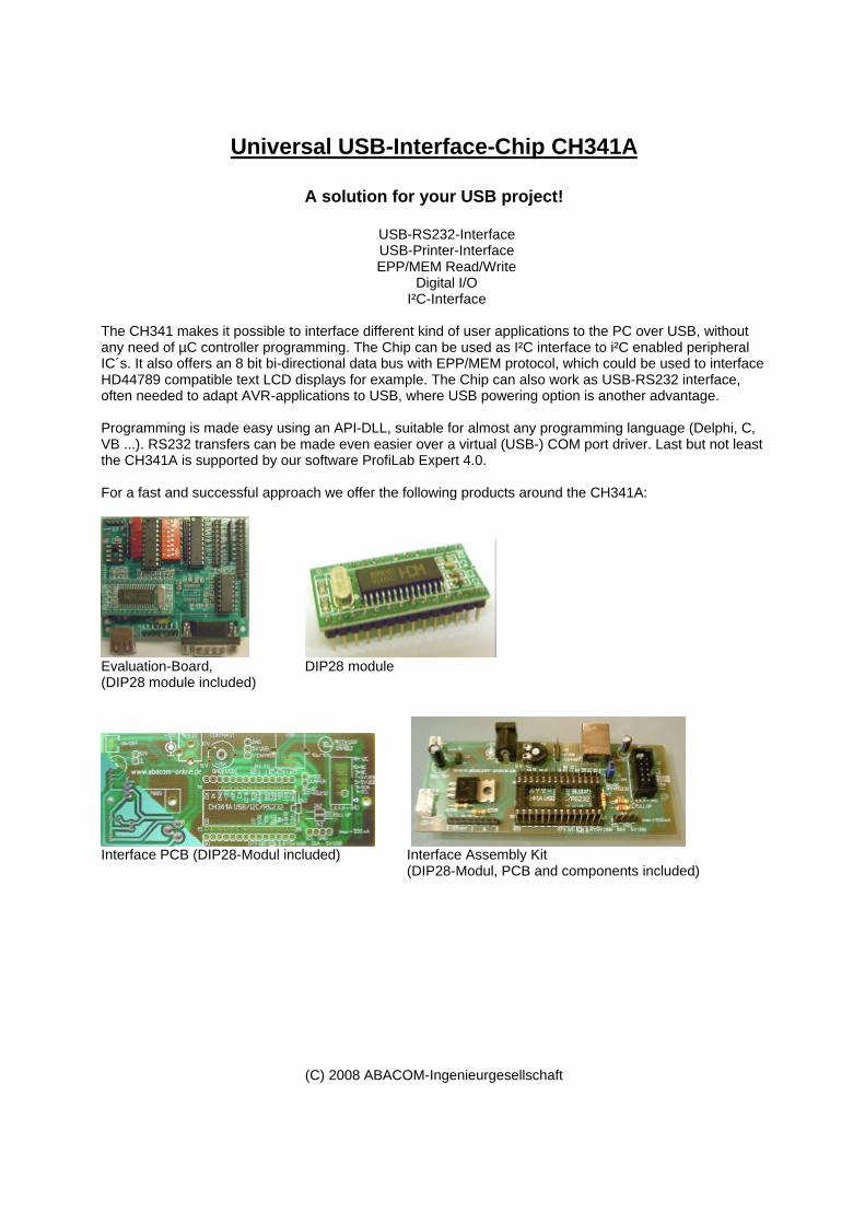
Mode configuration The chip is configurable for three basic modes. Depending on your circuit design the pins overtake different functional behaviour.
- UART - PRINT - EPP / MEM / I²C / Digital I/O
The mode configuration can be made using the pins SDA and SCL, or it can be stored in an optional serial EEPROM. Depending on the mode configuration the chip has a different USB-PID and Windows loads a certain device driver. Using an EEPROM an individual manufacturer ID and product ID can be used. Suitable EEPROMS are 24C01A, 24C02, 24C04, 24C16, etc. During initialization the chip tries to find an EEPROM configuration first. If no such configuration is found, SDA and SCL lines determine the mode (see table below). The EPP/MEM mode can be forced pulling the ACT# pin low to ground with a 2K resistor. The advantage is that I²C pins can still be used in that case. SCL and SDA conditions Mode USB-PID SDA and SCL open UART; RS232 5523 hex SDA low, SCL open EPP/MEM/I²C 5512 hex SDA with SCL shortened USB-Printer 5584 hex
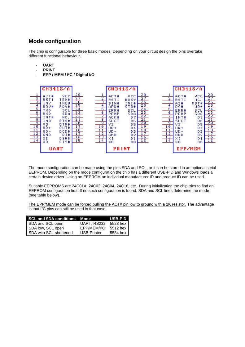
USB, power supply, clock, reset Pin Name Function Remarks 28 VCC Supply 0,1 µF to ground 12 GND Ground 9 V3 3,3 V supply: connect to VCC
5 V supply: 0,01 µF to GND 13 XI Osc. IN Osc. 12 MHz 14 XO Qsc OUT Osc 12 MHz 10 UD+ USB D+ USB line D+ 11 UD- USB D- USB line D- 1 ACT# Output LOW after USB init 2 RST1 Input External RESET input 24 SCL I²C SCL bus line 23 SDA I²C SDA bus line
Above circuit shows how to operate the CH341A. USB connection is P3. USB cables usually use the following colour encoding: VCC Red GND Black D+ Green D- White The chip is clocked with a 12 MHz crystal. The EEPROM is optional. The circuit is USB powered. L1 indicates ”Chip ready”. C26 generates a power-on-reset.
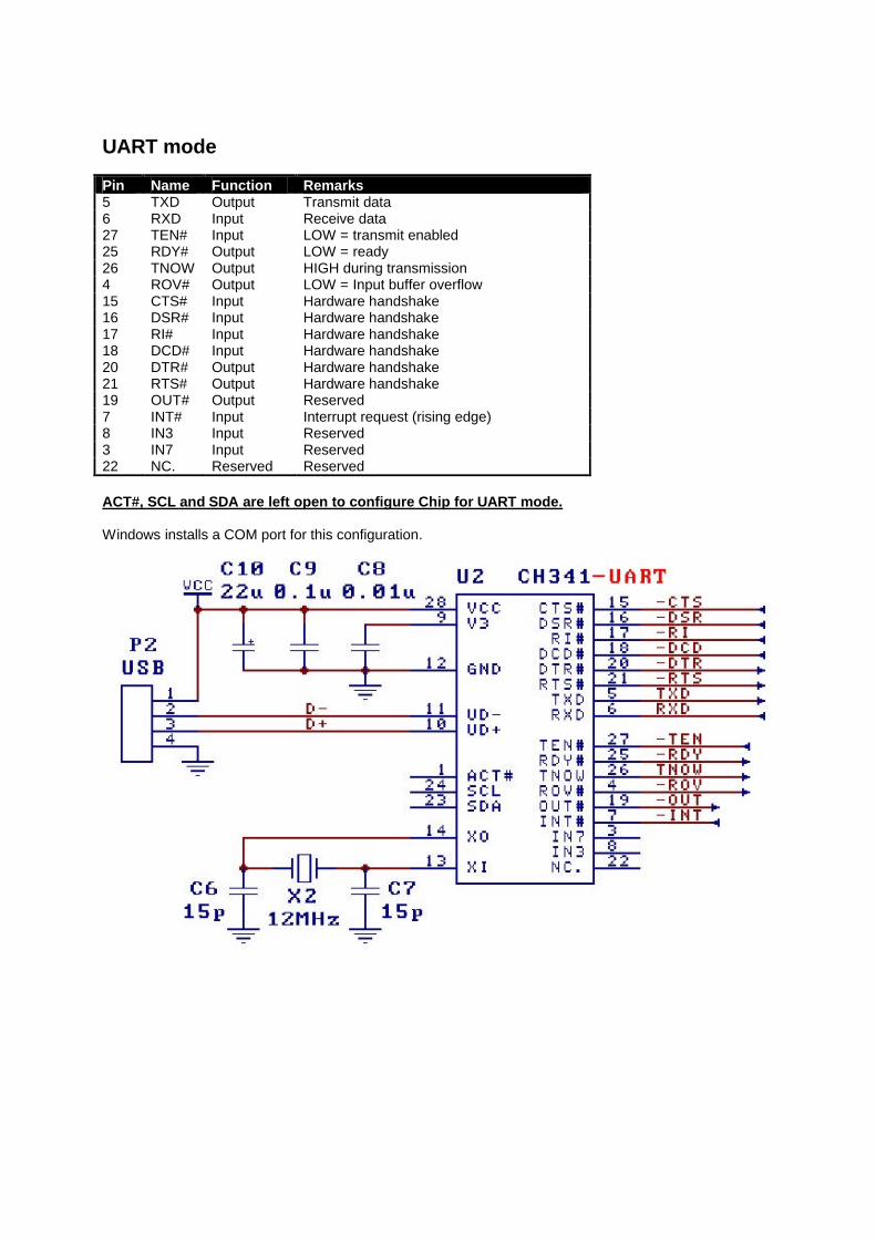
UART mode Pin Name Function Remarks 5 TXD Output Transmit data 6 RXD Input Receive data 27 TEN# Input LOW = transmit enabled 25 RDY# Output LOW = ready 26 TNOW Output HIGH during transmission 4 ROV# Output LOW = Input buffer overflow 15 CTS# Input Hardware handshake 16 DSR# Input Hardware handshake 17 RI# Input Hardware handshake 18 DCD# Input Hardware handshake 20 DTR# Output Hardware handshake 21 RTS# Output Hardware handshake 19 OUT# Output Reserved 7 INT# Input Interrupt request (rising edge) 8 IN3 Input Reserved 3 IN7 Input Reserved 22 NC. Reserved Reserved ACT#, SCL and SDA are left open to configure Chip for UART mode. Windows installs a COM port for this configuration.
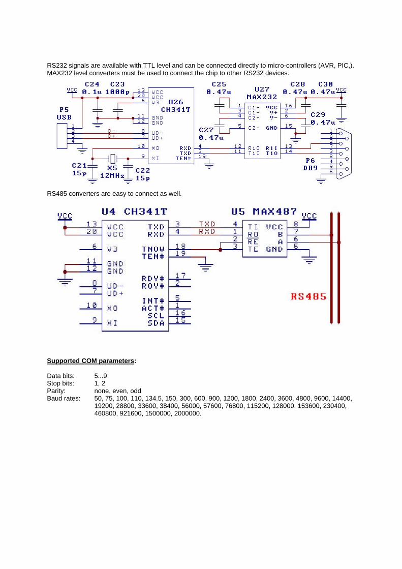
RS232 signals are available with TTL level and can be connected directly to micro-controllers (AVR, PIC,). MAX232 level converters must be used to connect the chip to other RS232 devices.
RS485 converters are easy to connect as well.
Supported COM parameters: Data bits: 5...9 Stop bits: 1, 2 Parity: none, even, odd Baud rates: 50, 75, 100, 110, 134.5, 150, 300, 600, 900, 1200, 1800, 2400, 3600, 4800, 9600, 14400,
19200, 28800, 33600, 38400, 56000, 57600, 76800, 115200, 128000, 153600, 230400, 460800, 921600, 1500000, 2000000.
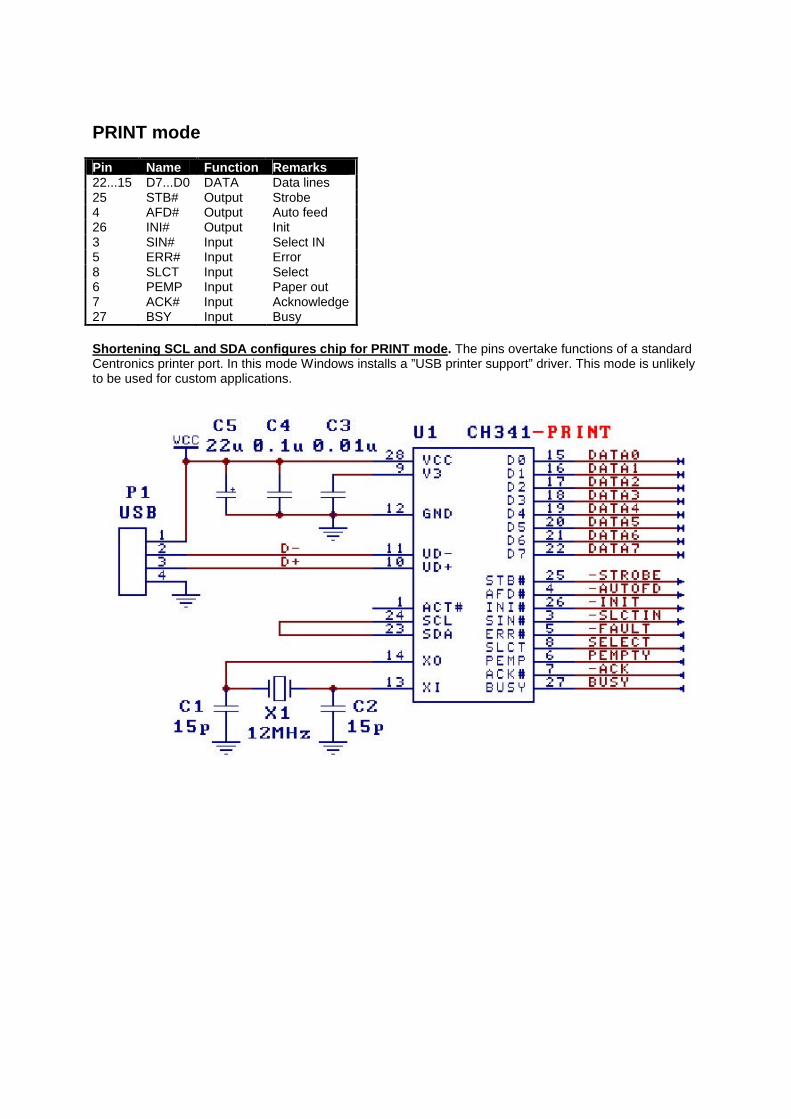
PRINT mode Pin Name Function Remarks 22...15 D7...D0 DATA Data lines 25 STB# Output Strobe 4 AFD# Output Auto feed 26 INI# Output Init 3 SIN# Input Select IN 5 ERR# Input Error 8 SLCT Input Select 6 PEMP Input Paper out 7 ACK# Input Acknowledge 27 BSY Input Busy Shortening SCL and SDA configures chip for PRINT mode. The pins overtake functions of a standard Centronics printer port. In this mode Windows installs a ”USB printer support” driver. This mode is unlikely to be used for custom applications.
EPP / MEM / I²C / I/O This mode can be configured in two different ways:
Pin 23 (SDA) connected to ground ( => I²C not possible ) or Pin 1 (ACT#) connected to Ground over 2K resistor
This mode configuration will load a Windows driver that can be accessed from programming languages using an API-DLL (CH341API.DLL). Examples and include-files are available for Delphi, VB und C. Calling an API-function the CH341A will do the data exchange with the connected peripherals itself. Depending on the called function and hardware protocol the chip will generate the necessary signal pattern at its pins. SCL (Pin 24) and SDA (Pin 23) are assigned to I²C. Other pins have different functions for EPP/MEM transfers. I/O pins can be programmed individually as well, to realize other hardware protocols by software programming.
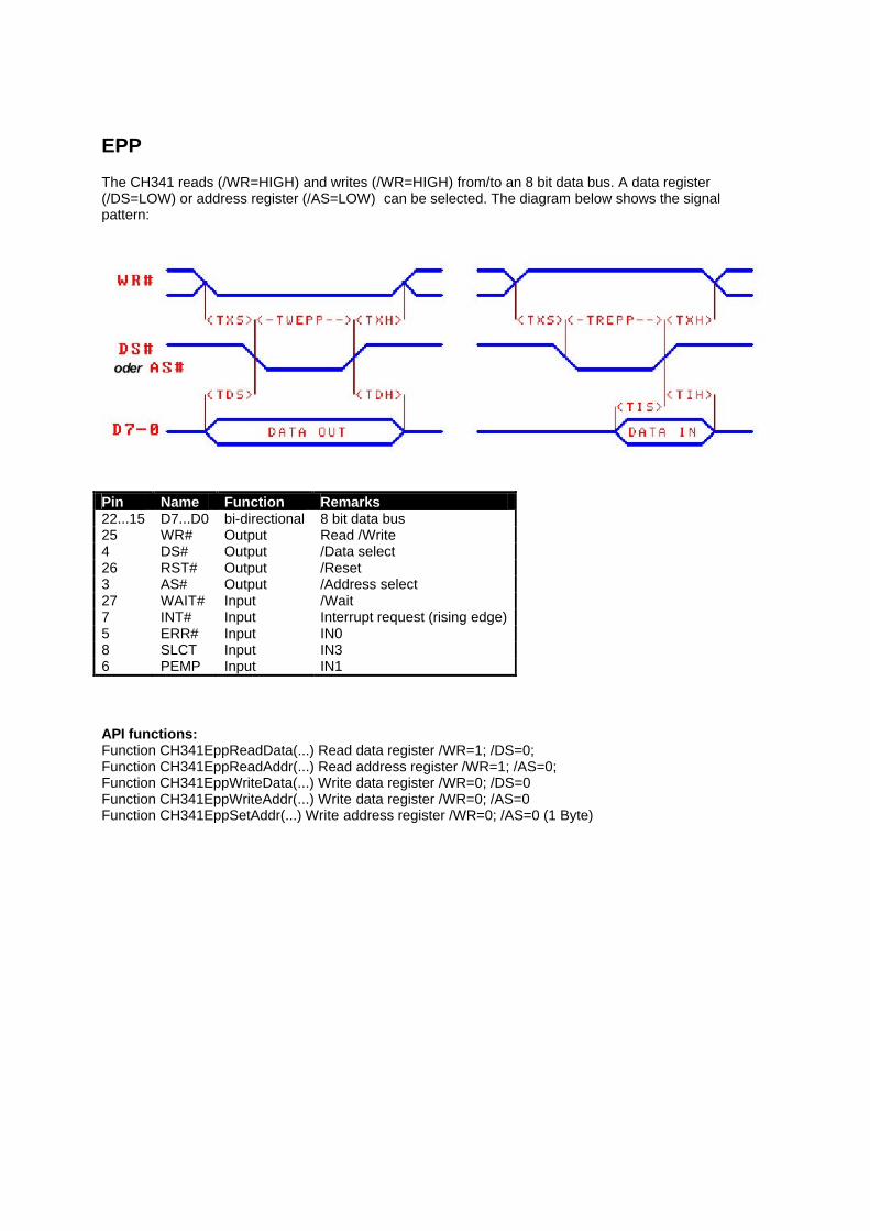
EPP The CH341 reads (/WR=HIGH) and writes (/WR=HIGH) from/to an 8 bit data bus. A data register (/DS=LOW) or address register (/AS=LOW) can be selected. The diagram below shows the signal pattern:
Pin Name Function Remarks 22...15 D7...D0 bi-directional 8 bit data bus 25 WR# Output Read /Write 4 DS# Output /Data select 26 RST# Output /Reset 3 AS# Output /Address select 27 WAIT# Input /Wait 7 INT# Input Interrupt request (rising edge) 5 ERR# Input IN0 8 SLCT Input IN3 6 PEMP Input IN1 API functions: Function CH341EppReadData(...) Read data register /WR=1; /DS=0; Function CH341EppReadAddr(...) Read address register /WR=1; /AS=0; Function CH341EppWriteData(...) Write data register /WR=0; /DS=0 Function CH341EppWriteAddr(...) Write data register /WR=0; /AS=0 Function CH341EppSetAddr(...) Write address register /WR=0; /AS=0 (1 Byte)
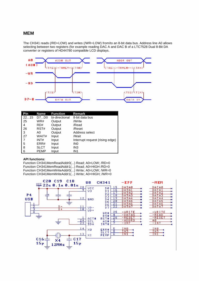
MEM The CH341 reads (/RD=LOW) and writes (/WR=LOW) from/to an 8-bit data bus. Address line A0 allows selecting between two registers (for example reading DAC A and DAC B of a LTC7528 Dual 8-Bit DA converter or registers of HD44780 compatible LCD displays.
Pin Name Function Remark 22...15 D7...D0 bi-directional 8-bit data bus 25 WR# Output /Write 4 RD# Output /Read 26 RST# Output /Reset 3 A0 Output Address select 27 WAIT# Input /Wait 7 INT# Input Interrupt request (rising edge) 5 ERR# Input IN0 8 SLCT Input IN3 6 PEMP Input IN1 API functions: Function CH341MemReadAddr0(...) Read; A0=LOW; /RD=0 Function CH341MemReadAddr1(...) Read; A0=HIGH /RD=0 Function CH341MemWriteAddr0(...) Write; A0=LOW; /WR=0 Function CH341MemWriteAddr1(...) Write; A0=HIGH; /WR=0
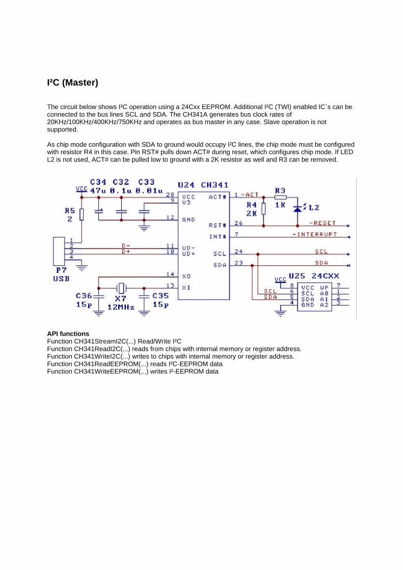
I²C (Master) The circuit below shows I²C operation using a 24Cxx EEPROM. Additional I²C (TWI) enabled IC´s can be connected to the bus lines SCL and SDA. The CH341A generates bus clock rates of 20KHz/100KHz/400KHz/750KHz and operates as bus master in any case. Slave operation is not supported. As chip mode configuration with SDA to ground would occupy I²C lines, the chip mode must be configured with resistor R4 in this case. Pin RST# pulls down ACT# during reset, which configures chip mode. If LED L2 is not used, ACT# can be pulled low to ground with a 2K resistor as well and R3 can be removed.
API functions Function CH341StreamI2C(...) Read/Write I²C Function CH341ReadI2C(...) reads from chips with internal memory or register address. Function CH341WriteI2C(...) writes to chips with internal memory or register address. Function CH341ReadEEPROM(...) reads I²C-EEPROM data Function CH341WriteEEPROM(...) writes I²-EEPROM data
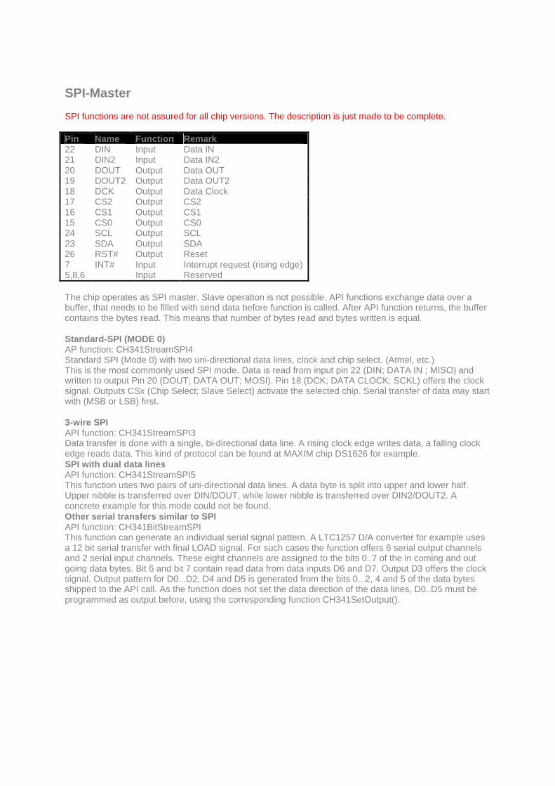
SPI-Master SPI functions are not assured for all chip versions. The description is just made to be complete. Pin Name Function Remark 22 DIN Input Data IN 21 DIN2 Input Data IN2 20 DOUT Output Data OUT 19 DOUT2 Output Data OUT2 18 DCK Output Data Clock 17 CS2 Output CS2 16 CS1 Output CS1 15 CS0 Output CS0 24 SCL Output SCL 23 SDA Output SDA 26 RST# Output Reset 7 INT# Input Interrupt request (rising edge) 5,8,6 Input Reserved The chip operates as SPI master. Slave operation is not possible. API functions exchange data over a buffer, that needs to be filled with send data before function is called. After API function returns, the buffer contains the bytes read. This means that number of bytes read and bytes written is equal. Standard-SPI (MODE 0) AP function: CH341StreamSPI4 Standard SPI (Mode 0) with two uni-directional data lines, clock and chip select. (Atmel, etc.) This is the most commonly used SPI mode. Data is read from input pin 22 (DIN; DATA IN ; MISO) and written to output Pin 20 (DOUT; DATA OUT; MOSI). Pin 18 (DCK; DATA CLOCK; SCKL) offers the clock signal. Outputs CSx (Chip Select; Slave Select) activate the selected chip. Serial transfer of data may start with (MSB or LSB) first. 3-wire SPI API function: CH341StreamSPI3 Data transfer is done with a single, bi-directional data line. A rising clock edge writes data, a falling clock edge reads data. This kind of protocol can be found at MAXIM chip DS1626 for example. SPI with dual data lines API function: CH341StreamSPI5 This function uses two pairs of uni-directional data lines. A data byte is split into upper and lower half. Upper nibble is transferred over DIN/DOUT, while lower nibble is transferred over DIN2/DOUT2. A concrete example for this mode could not be found. Other serial transfers similar to SPI API function: CH341BitStreamSPI This function can generate an individual serial signal pattern. A LTC1257 D/A converter for example uses a 12 bit serial transfer with final LOAD signal. For such cases the function offers 6 serial output channels and 2 serial input channels. These eight channels are assigned to the bits 0..7 of the in coming and out going data bytes. Bit 6 and bit 7 contain read data from data inputs D6 and D7. Output D3 offers the clock signal. Output pattern for D0...D2, D4 and D5 is generated from the bits 0...2, 4 and 5 of the data bytes shipped to the API call. As the function does not set the data direction of the data lines, D0..D5 must be programmed as output before, using the corresponding function CH341SetOutput().
Programming I/O individually Each I/O pin of the CH341A is assigned to a certain bit in the parameters Enable, SetDirOut and SetDataOut of the API functions listed below. 15 bi-directional pins (with programmable data direction; input or output): Bit 0-7 D0-D7 pin 15-22 Bit 8 ERR# pin 5 Bit 9 PEMP pin 6 Bit 10 ACK pin 7 Bit 11 SLCT pin 8 Bit 12 - - Bit 13 BUSY/WAIT# pin 27 Bit 14 AUTOFD#/DATAS# pin 4 Bit 15 SLCTIN#/ADDRS# pin 3 One pseudo-bi-directional pin (Combination of input and open-collector-output) : Bit 23 SDA pin 23 (functions GetInput/GetStatus) Bit 16 SDA pin 23 (function SetOutput) Three uni-directional pins (output only): Bit 16 RESET# pin 26 Bit 17 WRITE# pin 25 Bit 18 SCL pin pin 24 API functions CH341SetOutput
- Sets data direction (input/output) of bi-directional pins, - Sets output state HIGH/LOW
CH341Set_D5_D0
- Sets data direction of pins D0...D5 - Sets output state of pins D0...D5
CH341GetInput und CH341GetStatus
- Reads input states Parameter Enable
- Prohibits or allows changes of data direction - Bit set = changes allowed - Bit clear = changes are ignored
Parameter SetDirOut:
- Sets data direction: Input/Output - Bit set = Pin operates as output (Caution!) - Bit clear = Pin operates as input
Parameter SetDataOut
- Switch outputs - Bit set = switch output HIGH - Bit clear = switch output LOW
Example: CH341SetOutput( 0, $FF, $FF, $F0) sets data direction of D0...D7 to output. Other lines stay untouched. D0...3 are programmed LOW. D4...D7 are programmed HIGH.
Content of a optional configuration EEPROM Byte address Name Remarks Value 00 hex SIG 53H = Signature EEPROM valid 53 hex 01 hex MODE 23H = RS232 or 12H = EPP/MEM/PRINTER 23 hex or 12 hex 02 hex CFG Configuration, see next table FE hex 03 hex Reserved 00 hex 05…04 hex VID Vendor ID 4348 hex 07…06 hex PID Product ID 55xx hex 09…08 hex RID Release ID 0100 hex 17…10 hex SN Serial Number, eight characters 12345678 7F…20 hex PIDS Product name string 00 hex, 00 hex others 00 hex or FF hex Bit no. Name Remarks Value 7 PRT 0 = USB PRINTER; otherwise 1 1 6 PWR Power: 0 = external; 1 = USB 1 5 SN-S Serial number 0=valid; 1=invalid 1 4 PID-S Product string 0=valid; 1=invalid 1 3 SPD Printer data speed 0=high; 1=low 1 2 SUSP Suspend mode 0=prohibited; 1=permitted 1 1 PROT1 1 0 PROT0 0
API In CH341A mode EPP / MEM / I²C / Digital I/O the chip can be accessed with API function calls. Therefore CH341DLL.DLL needs to be imported. Examples for Delphi, C, Visual Basic and ProfiLab Expert are available. All API functions need to have the device number (iIndex) as first parameter. The first chip on USB is device number 0 (iIndex=0), the 2nd chip on USB is device 1, and so on. General functions Function CH341OpenDevice: Function connects to CH341A and needs to be called before other calls. Function CH341CloseDevice: Function terminates connection with CH341A. Function CH341ResetDevice: Function resets chip to power-on-state. Function CH341SetExclusive:
iExclusive: 0=shared ; 1=exclusive;
For Information on other API functions please refer to the examples
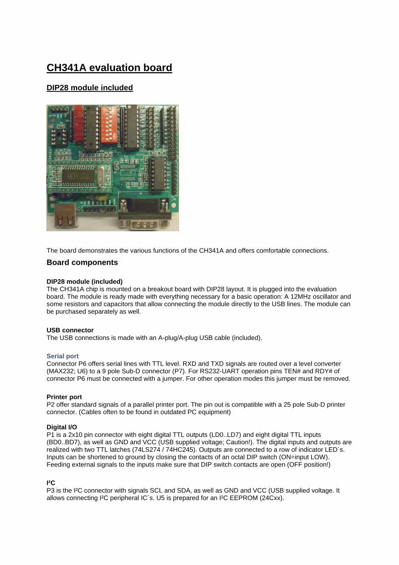
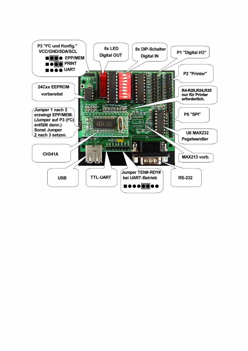
CH341A evaluation board DIP28 module included
The board demonstrates the various functions of the CH341A and offers comfortable connections.
Board components
DIP28 module (included) The CH341A chip is mounted on a breakout board with DIP28 layout. It is plugged into the evaluation board. The module is ready made with everything necessary for a basic operation: A 12MHz oscillator and some resistors and capacitors that allow connecting the module directly to the USB lines. The module can be purchased separately as well.
USB connector The USB connections is made with an A-plug/A-plug USB cable (included).
Serial port Connector P6 offers serial lines with TTL level. RXD and TXD signals are routed over a level converter (MAX232; U6) to a 9 pole Sub-D connector (P7). For RS232-UART operation pins TEN# and RDY# of connector P6 must be connected with a jumper. For other operation modes this jumper must be removed.
Printer port P2 offer standard signals of a parallel printer port. The pin out is compatible with a 25 pole Sub-D printer connector. (Cables often to be found in outdated PC equipment) Digital I/O P1 is a 2x10 pin connector with eight digital TTL outputs (LD0..LD7) and eight digital TTL inputs (BD0..BD7), as well as GND and VCC (USB supplied voltage; Caution!). The digital inputs and outputs are realized with two TTL latches (74LS274 / 74HC245). Outputs are connected to a row of indicator LED´s. Inputs can be shortened to ground by closing the contacts of an octal DIP switch (ON=input LOW). Feeding external signals to the inputs make sure that DIP switch contacts are open (OFF position!)
I²C P3 is the I²C connector with signals SCL and SDA, as well as GND and VCC (USB supplied voltage. It allows connecting I²C peripheral IC´s. U5 is prepared for an I²C EEPROM (24Cxx).
As long as no configuration EEPROM is used, the CH341A operation mode is determined with jumpers: Jumper SDA<->SCL present between P3 (3) – P3 (4): Operation mode PRINT Jumper removed P3 open: Operation mode UART Jumper SDA<->GND present between P3 (3) – P3 (2): Operation mode EPP/MEM/I²C/IO As I²C becomes occupied by jumper configuration, the operation mode EPP/MEM//I²C/IO can be configured as well connecting contacts 1 und 2 at port J1 with a jumper instead. This will connect pin1 (ACT#) und pin26 (RST#) of the CH341A with a 2K resistor.
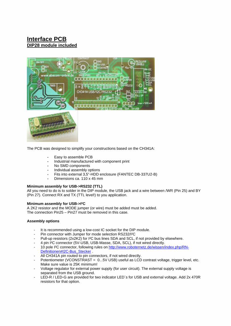
Interface PCB DIP28 module included
The PCB was designed to simplify your constructions based on the CH341A:
• Easy to assemble PCB • Industrial manufactured with component print • No SMD components • Individual assembly options
• Fits into external 3,5”-HDD enclosure (FANTEC DB-337U2-B) • Dimensions ca. 110 x 45 mm
Minimum assembly for USB->RS232 (TTL) All you need to do is to solder in the DIP module, the USB jack and a wire between /WR (Pin 25) and BY (Pin 27). Connect RX and TX (TTL level!) to you application. Minimum assembly for USB->I²C A 2K2 resistor and the MODE jumper (or wire) must be added must be added. The connection Pin25 – Pin27 must be removed in this case. Assembly options
- It is recommended using a low-cost IC socket for the DIP module. - Pin connector with Jumper for mode selection RS232/I²C - Pull-up resistors (2x2K2) for I²C bus lines SDA and SCL, if not provided by elsewhere. - 4 pin I²C connector (5V-USB, USB-Masse, SDA, SCL), if not wired directly. - 10 pole I²C connector, following rules on http://www.roboternetz.de/wissen/index.php/RN-
Definitionen#I2C-Bus_Stecker . - All CH341A pin routed to pin connectors, if not wired directly. - Potentiometer (VCONSTRAST = 0...5V USB) useful as LCD contrast voltage, trigger level, etc.
Make sure value is 25K minimum! - Voltage regulator for external power supply (for user circuit). The external supply voltage is
separated from the USB ground. - LED-R / LED-G are provided for two indicator LED´s for USB and external voltage. Add 2x 470R
resistors for that option.
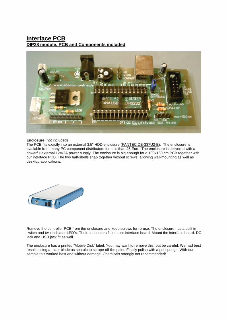
Interface PCB DIP28 module, PCB and Components included
Enclosure (not included) The PCB fits exactly into an external 3,5” HDD enclosure (FANTEC DB-337U2-B). The enclosure is available from many PC component distributors for less than 25 Euro. The enclosure is delivered with a powerful external 12V/2A power supply. The enclosure is big enough for a 100x160 cm PCB together with our interface PCB. The two half-shells snap together without screws, allowing wall-mounting as well as desktop applications.
Remove the controller PCB from the enclosure and keep screws for re-use. The enclosure has a built in switch and two indicator LED´s. Their connectors fit into our interface board. Mount the interface board. DC jack and USB jack fit as well. The enclosure has a printed ”Mobile Disk” label. You may want to remove this, but be careful. We had best results using a razor blade as spatula to scrape off the paint. Finally polish with a pot sponge. With our sample this worked best and without damage. Chemicals strongly not recommended!
Appendix: API functions (CH341DLL.DLL) // ************** // USB functions // ************** type mPCH341_NOTIFY_ROUTINE =ProceDure (iEventStatus:cardinal); stdcall; const CH341_DEVICE_ARRIVAL = 3 ; CH341_DEVICE_REMOVE_PEND = 1 ; CH341_DEVICE_REMOVE = 0 ; Function CH341SetDeviceNotify(iIndex:cardinal; iDeviceID: PCHAR; iNotifyRoutine:mPCH341_NOTIFY_ROUTINE):boolean;Stdcall; external 'CH341DLL.DLL'; // ********************* // General routines // ********************* // CH341A is addressed with ‘iIndex': // iIndex=0 => 1st CH341 @ USB // iIndex=1 => 2nd CH341 @ USB // iIndex=2 => 3rd ... // CH341OpenDevice: Connect to CH341A Function CH341OpenDevice(iIndex: cardinal): integer; Stdcall; external 'CH341DLL.DLL' ; // CH341CloseDevice: Terminate connection with CH341A procedure CH341CloseDevice(iIndex: cardinal); Stdcall; external 'CH341DLL.DLL'; // CH341ResetDevice: CH341A reset to power-on defaults Function CH341ResetDevice(iIndex: cardinal): boolean; Stdcall; external 'CH341DLL.DLL'; // CH341SetExclusive: //Allow/prevent re-open // iExclusive: 0=shared ; // 1=exclusive; Function CH341SetExclusive(iIndex:cardinal; iExclusive:cardinal ):boolean;Stdcall; external 'CH341DLL.DLL'; // ********************** // Information requests // ********************** Function CH341GetVersion: cardinal; Stdcall; external 'CH341DLL.DLL'; Function CH341DriverCommand(iIndex: cardinal; ioCommand: mPWIN32_COMMAND):cardinal; Stdcall; external 'CH341DLL.DLL'; Function CH341GetDrvVersion: cardinal; Stdcall; external 'CH341DLL.DLL'; Function CH341GetDeviceDescr(iIndex: cardinal; oBuffer: PVOID; ioLength: PULONG): boolean; Stdcall; external 'CH341DLL.DLL'; Function CH341GetConfigDescr(iIndex: cardinal; oBuffer: PVOID; ioLength: PULONG): boolean; Stdcall; external 'CH341DLL.DLL'; Function CH341GetDeviceName(iIndex:cardinal):PVOID;Stdcall; external 'CH341DLL.DLL'; Function CH341GetVerIC(iIndex:cardinal):cardinal;Stdcall; external 'CH341DLL.DLL'; // ********** // Interrupts // ********** Function CH341SetIntRoutine(iIndex: cardinal; iIntRoutine: mPCH341_INT_ROUTINE): boolean;Stdcall; external 'CH341DLL.DLL'; Function CH341ReadInter(iIndex: cardinal; iStatus:PULONG): boolean; Stdcall; external 'CH341DLL.DLL'; Function CH341AbortInter(iIndex: cardinal): boolean; Stdcall; external 'CH341DLL.DLL'; // Buffer (USB?) RS-232? Function CH341SetBufUpload(iIndex:cardinal; iEnableOrClear:cardinal ):boolean;Stdcall; external 'CH341DLL.DLL'; Function CH341QueryBufUpload(iIndex:cardinal):integer;Stdcall; external 'CH341DLL.DLL'; Function CH341SetBufDownload(iIndex:cardinal; iEnableOrClear:cardinal ):boolean;Stdcall; external 'CH341DLL.DLL'; Function CH341QueryBufDownload(iIndex:cardinal ):integer;Stdcall; external 'CH341DLL.DLL'; // (USB?) RS-232? Function CH341ResetInter(iIndex:cardinal ):boolean;Stdcall; external 'CH341DLL.DLL'; Function CH341ResetRead(iIndex:cardinal ):boolean;Stdcall; external 'CH341DLL.DLL'; Function CH341ResetWrite(iIndex:cardinal ):boolean;Stdcall; external 'CH341DLL.DLL'; // USB ? RS-232? //Delay; iDelay: Unit 1ms Function CH341SetDelaymS(iIndex:cardinal; iDelay:cardinal ):boolean;Stdcall; external 'CH341DLL.DLL'; //Timeout; iWriteTimeout: Unit 1ms
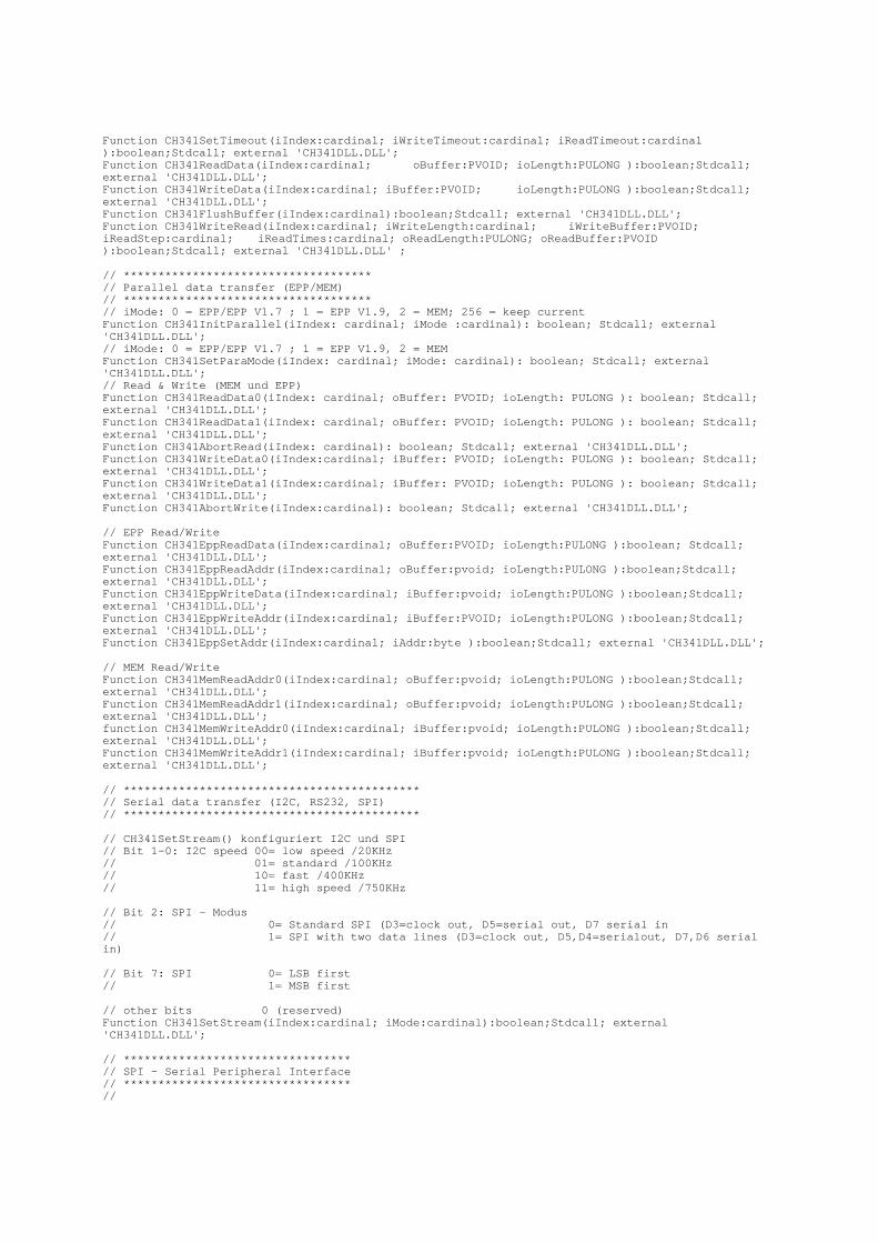
Function CH341SetTimeout(iIndex:cardinal; iWriteTimeout:cardinal; iReadTimeout:cardinal ):boolean;Stdcall; external 'CH341DLL.DLL'; Function CH341ReadData(iIndex:cardinal; oBuffer:PVOID; ioLength:PULONG ):boolean;Stdcall; external 'CH341DLL.DLL'; Function CH341WriteData(iIndex:cardinal; iBuffer:PVOID; ioLength:PULONG ):boolean;Stdcall; external 'CH341DLL.DLL'; Function CH341FlushBuffer(iIndex:cardinal):boolean;Stdcall; external 'CH341DLL.DLL'; Function CH341WriteRead(iIndex:cardinal; iWriteLength:cardinal; iWriteBuffer:PVOID; iReadStep:cardinal; iReadTimes:cardinal; oReadLength:PULONG; oReadBuffer:PVOID ):boolean;Stdcall; external 'CH341DLL.DLL' ; // ************************************ // Parallel data transfer (EPP/MEM) // ************************************ // iMode: 0 = EPP/EPP V1.7 ; 1 = EPP V1.9, 2 = MEM; 256 = keep current Function CH341InitParallel(iIndex: cardinal; iMode :cardinal): boolean; Stdcall; external 'CH341DLL.DLL'; // iMode: 0 = EPP/EPP V1.7 ; 1 = EPP V1.9, 2 = MEM Function CH341SetParaMode(iIndex: cardinal; iMode: cardinal): boolean; Stdcall; external 'CH341DLL.DLL'; // Read & Write (MEM und EPP) Function CH341ReadData0(iIndex: cardinal; oBuffer: PVOID; ioLength: PULONG ): boolean; Stdcall; external 'CH341DLL.DLL'; Function CH341ReadData1(iIndex: cardinal; oBuffer: PVOID; ioLength: PULONG ): boolean; Stdcall; external 'CH341DLL.DLL'; Function CH341AbortRead(iIndex: cardinal): boolean; Stdcall; external 'CH341DLL.DLL'; Function CH341WriteData0(iIndex:cardinal; iBuffer: PVOID; ioLength: PULONG ): boolean; Stdcall; external 'CH341DLL.DLL'; Function CH341WriteData1(iIndex:cardinal; iBuffer: PVOID; ioLength: PULONG ): boolean; Stdcall; external 'CH341DLL.DLL'; Function CH341AbortWrite(iIndex:cardinal): boolean; Stdcall; external 'CH341DLL.DLL'; // EPP Read/Write Function CH341EppReadData(iIndex:cardinal; oBuffer:PVOID; ioLength:PULONG ):boolean; Stdcall; external 'CH341DLL.DLL'; Function CH341EppReadAddr(iIndex:cardinal; oBuffer:pvoid; ioLength:PULONG ):boolean;Stdcall; external 'CH341DLL.DLL'; Function CH341EppWriteData(iIndex:cardinal; iBuffer:pvoid; ioLength:PULONG ):boolean;Stdcall; external 'CH341DLL.DLL'; Function CH341EppWriteAddr(iIndex:cardinal; iBuffer:PVOID; ioLength:PULONG ):boolean;Stdcall; external 'CH341DLL.DLL'; Function CH341EppSetAddr(iIndex:cardinal; iAddr:byte ):boolean;Stdcall; external 'CH341DLL.DLL'; // MEM Read/Write Function CH341MemReadAddr0(iIndex:cardinal; oBuffer:pvoid; ioLength:PULONG ):boolean;Stdcall; external 'CH341DLL.DLL'; Function CH341MemReadAddr1(iIndex:cardinal; oBuffer:pvoid; ioLength:PULONG ):boolean;Stdcall; external 'CH341DLL.DLL'; function CH341MemWriteAddr0(iIndex:cardinal; iBuffer:pvoid; ioLength:PULONG ):boolean;Stdcall; external 'CH341DLL.DLL'; Function CH341MemWriteAddr1(iIndex:cardinal; iBuffer:pvoid; ioLength:PULONG ):boolean;Stdcall; external 'CH341DLL.DLL'; // ******************************************* // Serial data transfer (I2C, RS232, SPI) // ******************************************* // CH341SetStream() konfiguriert I2C und SPI // Bit 1-0: I2C speed 00= low speed /20KHz // 01= standard /100KHz // 10= fast /400KHz // 11= high speed /750KHz // Bit 2: SPI - Modus // 0= Standard SPI (D3=clock out, D5=serial out, D7 serial in // 1= SPI with two data lines (D3=clock out, D5,D4=serialout, D7,D6 serial in) // Bit 7: SPI 0= LSB first // 1= MSB first // other bits 0 (reserved) Function CH341SetStream(iIndex:cardinal; iMode:cardinal):boolean;Stdcall; external 'CH341DLL.DLL'; // ********************************* // SPI - Serial Peripheral Interface // ********************************* //
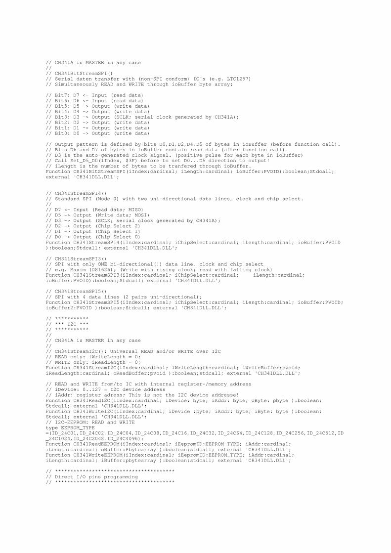
// CH341A is MASTER in any case // // CH341BitStreamSPI() // Serial daten transfer with (non-SPI conform) IC´s (e.g. LTC1257) // Simultaneously READ and WRITE through ioBuffer byte array: // Bit7: D7 <- Input (read data) // Bit6: D6 <- Input (read data) // Bit5: D5 -> Output (write data) // Bit4: D4 -> Output (write data) // Bit3: D3 -> Output (SCLK; serial clock generated by CH341A); // Bit2: D2 -> Output (write data) // Bit1: D1 -> Output (write data) // Bit0: D0 -> Output (write data) // Output pattern is defined by bits D0,D1,D2,D4,D5 of bytes in ioBuffer (before function call). // Bits D6 and D7 of bytes in ioBuffer contain read data (after function call). // D3 is the auto-generated clock signal. (positive pulse for each byte in ioBuffer) // Call Set_D5_D0(iIndex, $3F) before to set D0...D5 direction to output! // iLength is the number of bytes to be tranfered through ioBuffer. Function CH341BitStreamSPI(iIndex:cardinal; iLength:cardinal; ioBuffer:PVOID):boolean;Stdcall; external 'CH341DLL.DLL'; // CH341StreamSPI4() // Standard SPI (Mode 0) with two uni-directional data lines, clock and chip select. // // D7 <- Input (Read data; MISO) // D5 -> Output (Write data; MOSI) // D3 -> Output (SCLK; serial clock generated by CH341A); // D2 -> Output (Chip Select 2) // D1 -> Output (Chip Select 1) // D0 -> Output (Chip Select 0) Function CH341StreamSPI4(iIndex:cardinal; iChipSelect:cardinal; iLength:cardinal; ioBuffer:PVOID ):boolean;Stdcall; external 'CH341DLL.DLL'; // CH341StreamSPI3() // SPI with only ONE bi-directional(!) data line, clock and chip select // e.g. Maxim (DS1626); (Write with rising clock; read with falling clock) Function CH341StreamSPI3(iIndex:cardinal; iChipSelect:cardinal; iLength:cardinal; ioBuffer:PVOID):boolean;Stdcall; external 'CH341DLL.DLL'; // CH341StreamSPI5() // SPI with 4 data lines (2 pairs uni-directional); Function CH341StreamSPI5(iIndex:cardinal; iChipSelect:cardinal; iLength:cardinal; ioBuffer:PVOID; ioBuffer2:PVOID ):boolean;Stdcall; external 'CH341DLL.DLL'; // *********** // *** I2C *** // *********** // // CH341A is MASTER in any case // // CH341StreamI2C(): Universal READ and/or WRITE over I2C // READ only: iWriteLength = 0; // WRITE only: iReadLength = 0; Function CH341StreamI2C(iIndex:cardinal; iWriteLength:cardinal; iWriteBuffer:pvoid; iReadLength:cardinal; oReadBuffer:pvoid ):boolean;stdcall; external 'CH341DLL.DLL'; // READ and WRITE from/to IC with internal register-/memory address // iDevice: 0..127 = I2C device address // iAddr: register adress; This is not the I2C device addresse! Function CH341ReadI2C(iIndex:cardinal; iDevice: byte; iAddr: byte; oByte: pbyte ):boolean; Stdcall; external 'CH341DLL.DLL'; Function CH341WriteI2C(iIndex:cardinal; iDevice :byte; iAddr: byte; iByte: byte ):boolean; Stdcall; external 'CH341DLL.DLL'; // I2C-EEPROM: READ and WRITE type EEPROM_TYPE =(ID_24C01,ID_24C02,ID_24C04,ID_24C08,ID_24C16,ID_24C32,ID_24C64,ID_24C128,ID_24C256,ID_24C512,ID_24C1024,ID_24C2048,ID_24C4096); Function CH341ReadEEPROM(iIndex:cardinal; iEepromID:EEPROM_TYPE; iAddr:cardinal; iLength:cardinal; oBuffer:Pbytearray ):boolean;stdcall; external 'CH341DLL.DLL'; Function CH341WriteEEPROM(iIndex:cardinal; iEepromID:EEPROM_TYPE; iAddr:cardinal; iLength:cardinal; iBuffer:pbytearray ):boolean;stdcall; external 'CH341DLL.DLL'; // *************************************** // Direct I/O pins programming // ***************************************
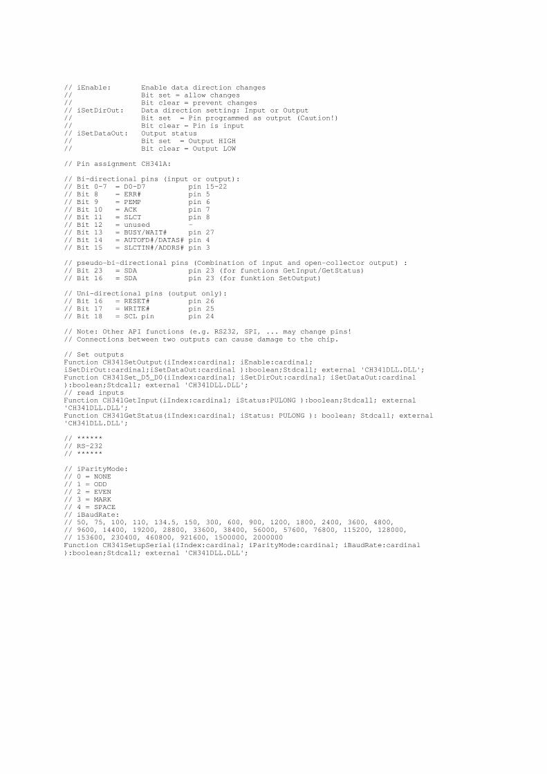
// iEnable: Enable data direction changes // Bit set = allow changes // Bit clear = prevent changes // iSetDirOut: Data direction setting: Input or Output // Bit set = Pin programmed as output (Caution!) // Bit clear = Pin is input // iSetDataOut: Output status // Bit set = Output HIGH // Bit clear = Output LOW // Pin assignment CH341A: // Bi-directional pins (input or output): // Bit 0-7 = D0-D7 pin 15-22 // Bit 8 = ERR# pin 5 // Bit 9 = PEMP pin 6 // Bit 10 = ACK pin 7 // Bit 11 = SLCT pin 8 // Bit 12 = unused - // Bit 13 = BUSY/WAIT# pin 27 // Bit 14 = AUTOFD#/DATAS# pin 4 // Bit 15 = SLCTIN#/ADDRS# pin 3 // pseudo-bi-directional pins (Combination of input and open-collector output) : // Bit 23 = SDA pin 23 (for functions GetInput/GetStatus) // Bit 16 = SDA pin 23 (for funktion SetOutput) // Uni-directional pins (output only): // Bit 16 = RESET# pin 26 // Bit 17 = WRITE# pin 25 // Bit 18 = SCL pin pin 24 // Note: Other API functions (e.g. RS232, SPI, ... may change pins! // Connections between two outputs can cause damage to the chip. // Set outputs Function CH341SetOutput(iIndex:cardinal; iEnable:cardinal; iSetDirOut:cardinal;iSetDataOut:cardinal ):boolean;Stdcall; external 'CH341DLL.DLL'; Function CH341Set_D5_D0(iIndex:cardinal; iSetDirOut:cardinal; iSetDataOut:cardinal ):boolean;Stdcall; external 'CH341DLL.DLL'; // read inputs Function CH341GetInput(iIndex:cardinal; iStatus:PULONG ):boolean;Stdcall; external 'CH341DLL.DLL'; Function CH341GetStatus(iIndex:cardinal; iStatus: PULONG ): boolean; Stdcall; external 'CH341DLL.DLL'; // ****** // RS-232 // ****** // iParityMode: // 0 = NONE // 1 = ODD // 2 = EVEN // 3 = MARK // 4 = SPACE // iBaudRate: // 50, 75, 100, 110, 134.5, 150, 300, 600, 900, 1200, 1800, 2400, 3600, 4800, // 9600, 14400, 19200, 28800, 33600, 38400, 56000, 57600, 76800, 115200, 128000, // 153600, 230400, 460800, 921600, 1500000, 2000000 Function CH341SetupSerial(iIndex:cardinal; iParityMode:cardinal; iBaudRate:cardinal ):boolean;Stdcall; external 'CH341DLL.DLL';