Universal ultrafast detector for short optical pulses ... · Universal ultrafast detector for short...
8
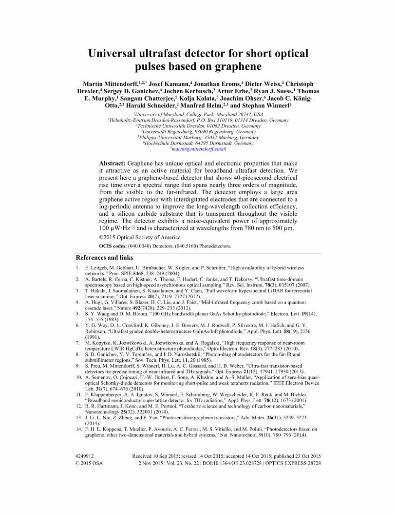
Universal ultrafast detector for short optical pulses based on graphene Martin Mittendorff, 1,2,* Josef Kamann, 4 Jonathan Eroms, 4 Dieter Weiss, 4 Christoph Drexler, 4 Sergey D. Ganichev, 4 Jochen Kerbusch, 2 Artur Erbe, 2 Ryan J. Suess, 1 Thomas E. Murphy, 1 Sangam Chatterjee, 5 Kolja Kolata, 5 Joachim Ohser, 6 Jacob C. König- Otto, 2,3 Harald Schneider, 2 Manfred Helm, 2,3 and Stephan Winnerl 2 1 University of Maryland, College Park, Maryland 20742, USA 2 Helmholtz-Zentrum Dresden-Rossendorf, P.O. Box 510119, 01314 Dresden, Germany 3 Technische Universität Dresden, 01062 Dresden, Germany 4 Universität Regensburg, 93040 Regensburg, Germany 5 Philipps-Universität Marburg, 35032 Marburg, Germany 6 Hochschule Darmstadt, 64295 Darmstadt, Germany * [email protected] Abstract: Graphene has unique optical and electronic properties that make it attractive as an active material for broadband ultrafast detection. We present here a graphene-based detector that shows 40-picosecond electrical rise time over a spectral range that spans nearly three orders of magnitude, from the visible to the far-infrared. The detector employs a large area graphene active region with interdigitated electrodes that are connected to a log-periodic antenna to improve the long-wavelength collection efficiency, and a silicon carbide substrate that is transparent throughout the visible regime. The detector exhibits a noise-equivalent power of approximately 100 μW·Hz –½ and is characterized at wavelengths from 780 nm to 500 μm. ©2015 Optical Society of America OCIS codes: (040.0040) Detectors; (040.5160) Photodetectors. References and links 1. E. Leitgeb, M. Gebhart, U. Birnbacher, W. Kogler, and P. Schrotter, “High availability of hybrid wireless networks,” Proc. SPIE 5465, 238–249 (2004). 2. A. Bartels, R. Cerna, C. Kistner, A. Thoma, F. Hudert, C. Janke, and T. Dekorsy, “Ultrafast time-domain spectroscopy based on high-speed asynchronous optical sampling,” Rev. Sci. Instrum. 78(3), 035107 (2007). 3. T. Hakala, J. Suomalainen, S. Kaasalainen, and Y. Chen, “Full waveform hyperspectral LiDAR for terrestrial laser scanning,” Opt. Express 20(7), 7119–7127 (2012). 4. A. Hugi, G. Villares, S. Blaser, H. C. Liu, and J. Faist, “Mid-infrared frequency comb based on a quantum cascade laser,” Nature 492(7428), 229–233 (2012). 5. S. Y. Wang and D. M. Bloom, “100 GHz bandwidth planar GaAs Schottky photodiode,” Electron. Lett. 19(14), 554–555 (1983). 6. Y. G. Wey, D. L. Crawford, K. Giboney, J. E. Bowers, M. J. Rodwell, P. Silvestre, M. J. Hafich, and G. Y. Robinson, “Ultrafast graded double‐heterostructure GaInAs/InP photodiode,” Appl. Phys. Lett. 58(19), 2156 (1991). 7. M. Kopytko, K. Jozwikowski, A. Jozwikowska, and A. Rogalski, “High frequency response of near-room temperature LWIR HgCdTe heterostructure photodiodes,” Opto-Electron. Rev. 18(3), 277–283 (2010). 8. S. D. Ganichev, Y. V. Terent’ev, and I. D. Yaroshetskii, “Photon-drag photodetectors for the far-IR and submillimeter regions,” Sov. Tech. Phys. Lett. 11, 20 (1985). 9. S. Preu, M. Mittendorff, S. Winnerl, H. Lu, A. C. Gossard, and H. B. Weber, “Ultra-fast transistor-based detectors for precise timing of near infrared and THz signals,” Opt. Express 21(15), 17941–17950 (2013). 10. A. Semenov, O. Cojocari, H.-W. Hübers, F. Song, A. Klushin, and A.-S. Müller, “Application of zero-bias quasi- optical Schottky-diode detectors for monitoring short-pulse and weak terahertz radiation,” IEEE Electron Device Lett. 31(7), 674–676 (2010). 11. F. Klappenberger, A. A. Ignatov, S. Winnerl, E. Schomburg, W. Wegscheider, K. F. Renk, and M. Bichler, “Broadband semiconductor superlattice detector for THz radiation,” Appl. Phys. Lett. 78(12), 1673 (2001). 12. R. R. Hartmann, J. Kono, and M. E. Portnoi, “Terahertz science and technology of carbon nanomaterials,” Nanotechnology 25(32), 322001 (2014). 13. J. Li, L. Niu, Z. Zheng, and F. Yan, “Photosensitive graphene transistors,” Adv. Mater. 26(31), 5239–5273 (2014). 14. F. H. L. Koppens, T. Mueller, P. Avouris, A. C. Ferrari, M. S. Vitiello, and M. Polini, “Photodetectors based on graphene, other two-dimensional materials and hybrid systems,” Nat. Nanotechnol. 9(10), 780–793 (2014). #249912 Received 10 Sep 2015; revised 14 Oct 2015; accepted 14 Oct 2015; published 23 Oct 2015 © 2015 OSA 2 Nov 2015 | Vol. 23, No. 22 | DOI:10.1364/OE.23.028728 | OPTICS EXPRESS 28728
-
Upload
nguyenkhanh -
Category
Documents
-
view
222 -
download
0
Transcript of Universal ultrafast detector for short optical pulses ... · Universal ultrafast detector for short...
Universal ultrafast detector for short optical pulses based on graphene
Martin Mittendorff,1,2,* Josef Kamann,4 Jonathan Eroms,4 Dieter Weiss,4 Christoph Drexler,4 Sergey D. Ganichev,4 Jochen Kerbusch,2 Artur Erbe,2 Ryan J. Suess,1 Thomas
E. Murphy,1 Sangam Chatterjee,5 Kolja Kolata,5 Joachim Ohser,6 Jacob C. König-Otto,2,3 Harald Schneider,2 Manfred Helm,2,3 and Stephan Winnerl2
1University of Maryland, College Park, Maryland 20742, USA 2Helmholtz-Zentrum Dresden-Rossendorf, P.O. Box 510119, 01314 Dresden, Germany
3Technische Universität Dresden, 01062 Dresden, Germany 4Universität Regensburg, 93040 Regensburg, Germany
5Philipps-Universität Marburg, 35032 Marburg, Germany 6Hochschule Darmstadt, 64295 Darmstadt, Germany
Abstract: Graphene has unique optical and electronic properties that make it attractive as an active material for broadband ultrafast detection. We present here a graphene-based detector that shows 40-picosecond electrical rise time over a spectral range that spans nearly three orders of magnitude, from the visible to the far-infrared. The detector employs a large area graphene active region with interdigitated electrodes that are connected to a log-periodic antenna to improve the long-wavelength collection efficiency, and a silicon carbide substrate that is transparent throughout the visible regime. The detector exhibits a noise-equivalent power of approximately 100 µW·Hz–½ and is characterized at wavelengths from 780 nm to 500 µm.
©2015 Optical Society of America
OCIS codes: (040.0040) Detectors; (040.5160) Photodetectors.
References and links
1. E. Leitgeb, M. Gebhart, U. Birnbacher, W. Kogler, and P. Schrotter, “High availability of hybrid wireless networks,” Proc. SPIE 5465, 238–249 (2004).
2. A. Bartels, R. Cerna, C. Kistner, A. Thoma, F. Hudert, C. Janke, and T. Dekorsy, “Ultrafast time-domain spectroscopy based on high-speed asynchronous optical sampling,” Rev. Sci. Instrum. 78(3), 035107 (2007).
3. T. Hakala, J. Suomalainen, S. Kaasalainen, and Y. Chen, “Full waveform hyperspectral LiDAR for terrestrial laser scanning,” Opt. Express 20(7), 7119–7127 (2012).
4. A. Hugi, G. Villares, S. Blaser, H. C. Liu, and J. Faist, “Mid-infrared frequency comb based on a quantum cascade laser,” Nature 492(7428), 229–233 (2012).
5. S. Y. Wang and D. M. Bloom, “100 GHz bandwidth planar GaAs Schottky photodiode,” Electron. Lett. 19(14),554–555 (1983).
6. Y. G. Wey, D. L. Crawford, K. Giboney, J. E. Bowers, M. J. Rodwell, P. Silvestre, M. J. Hafich, and G. Y. Robinson, “Ultrafast graded double‐heterostructure GaInAs/InP photodiode,” Appl. Phys. Lett. 58(19), 2156(1991).
7. M. Kopytko, K. Jozwikowski, A. Jozwikowska, and A. Rogalski, “High frequency response of near-room temperature LWIR HgCdTe heterostructure photodiodes,” Opto-Electron. Rev. 18(3), 277–283 (2010).
8. S. D. Ganichev, Y. V. Terent’ev, and I. D. Yaroshetskii, “Photon-drag photodetectors for the far-IR and submillimeter regions,” Sov. Tech. Phys. Lett. 11, 20 (1985).
9. S. Preu, M. Mittendorff, S. Winnerl, H. Lu, A. C. Gossard, and H. B. Weber, “Ultra-fast transistor-based detectors for precise timing of near infrared and THz signals,” Opt. Express 21(15), 17941–17950 (2013).
10. A. Semenov, O. Cojocari, H.-W. Hübers, F. Song, A. Klushin, and A.-S. Müller, “Application of zero-bias quasi-optical Schottky-diode detectors for monitoring short-pulse and weak terahertz radiation,” IEEE Electron Device Lett. 31(7), 674–676 (2010).
11. F. Klappenberger, A. A. Ignatov, S. Winnerl, E. Schomburg, W. Wegscheider, K. F. Renk, and M. Bichler, “Broadband semiconductor superlattice detector for THz radiation,” Appl. Phys. Lett. 78(12), 1673 (2001).
12. R. R. Hartmann, J. Kono, and M. E. Portnoi, “Terahertz science and technology of carbon nanomaterials,” Nanotechnology 25(32), 322001 (2014).
13. J. Li, L. Niu, Z. Zheng, and F. Yan, “Photosensitive graphene transistors,” Adv. Mater. 26(31), 5239–5273(2014).
14. F. H. L. Koppens, T. Mueller, P. Avouris, A. C. Ferrari, M. S. Vitiello, and M. Polini, “Photodetectors based on graphene, other two-dimensional materials and hybrid systems,” Nat. Nanotechnol. 9(10), 780–793 (2014).
#249912 Received 10 Sep 2015; revised 14 Oct 2015; accepted 14 Oct 2015; published 23 Oct 2015 © 2015 OSA 2 Nov 2015 | Vol. 23, No. 22 | DOI:10.1364/OE.23.028728 | OPTICS EXPRESS 28728

15. F. Bonaccorso, Z. Sun, T. Hasan, and A. C. Ferrari, “Graphene photonics and optoelectronics,” Nat. Photonics 4(9), 611–622 (2010).
16. C. B. McKitterick, H. Vora, X. Du, B. S. Karasik, and D. E. Prober, “Graphene microbolometers with superconducting contacts for terahertz photon detection,” J. Low Temp. Phys. 176(3-4), 291–298 (2014).
17. Y. Yao, R. Shankar, P. Rauter, Y. Song, J. Kong, M. Loncar, and F. Capasso, “High-responsivity mid-infrared graphene detectors with antenna-enhanced photocarrier generation and collection,” Nano Lett. 14(7), 3749–3754 (2014).
18. L. Vicarelli, M. S. Vitiello, D. Coquillat, A. Lombardo, A. C. Ferrari, W. Knap, M. Polini, V. Pellegrini, and A. Tredicucci, “Graphene field-effect transistors as room-temperature terahertz detectors,” Nat. Mater. 11(10), 865–871 (2012).
19. A. Zak, M. A. Andersson, M. Bauer, J. Matukas, A. Lisauskas, H. G. Roskos, and J. Stake, “Antenna-integrated 0.6 THz FET direct detectors based on CVD graphene,” Nano Lett. 14(10), 5834–5838 (2014).
20. X. Xu, N. M. Gabor, J. S. Alden, A. M. van der Zande, and P. L. McEuen, “Photo-thermoelectric effect at a graphene interface junction,” Nano Lett. 10(2), 562–566 (2010).
21. X. Cai, A. B. Sushkov, R. J. Suess, M. M. Jadidi, G. S. Jenkins, L. O. Nyakiti, R. L. Myers-Ward, S. Li, J. Yan, D. K. Gaskill, T. E. Murphy, H. D. Drew, and M. S. Fuhrer, “Sensitive room-temperature terahertz detection via the photothermoelectric effect in graphene,” Nat. Nanotechnol. 9(10), 814–819 (2014).
22. N. M. Gabor, J. C. W. Song, Q. Ma, N. L. Nair, T. Taychatanapat, K. Watanabe, T. Taniguchi, L. S. Levitov, and P. Jarillo-Herrero, “Hot carrier-assisted intrinsic photoresponse in graphene,” Science 334(6056), 648–652 (2011).
23. T. Mueller, F. Xia, and P. Avouris, “Graphene photodetectors for high-speed optical communications,” Nat. Photonics 4(5), 297–301 (2010).
24. M. Mittendorff, S. Winnerl, J. Kamann, J. Eroms, D. Weiss, H. Schneider, and M. Helm, “Ultrafast graphene-based broadband THz detector,” Appl. Phys. Lett. 103(2), 021113 (2013).
25. W. R. L. Lambrecht, S. Limpijumnong, S. N. Rashkeev, and B. Segall, “Electronic band structure of SiC polytypes: a discussion of theory and experiment,” Phys. Status Solidi B 202(1), 5–33 (1997).
26. S. D. Ganichev, “Tunnel ionization of deep impurities in semiconductors induced by terahertz electric fields,” Physica B 273, 737–742 (1999).
27. E. Ziemann, S. D. Ganichev, W. Prettl, I. N. Yassievich, and V. I. Perel, “Characterization of deep impurities in semiconductors by terahertz tunneling ionization,” J. Appl. Phys. 87(8), 3843 (2000).
28. W. G. Spitzer, D. Kleinman, and D. Walsh, “Electronic infrared properties of hexagonal silicon carbide,” Phys. Rev. 113(1), 127–132 (1959).
29. K. F. Mak, L. Ju, F. Wang, and T. F. Heinz, “Optical spectroscopy of graphene: From the far infrared to the ultraviolet,” Solid State Commun. 152(15), 1341–1349 (2012).
30. M. M. Glazov and S. D. Ganichev, “High frequency electric field induced nonlinear effects in graphene,” Phys. Rep. 535(3), 101–138 (2014).
31. Q. Han, T. Gao, R. Zhang, Y. Chen, J. Chen, G. Liu, Y. Zhang, Z. Liu, X. Wu, and D. Yu, “Highly sensitive hot electron bolometer based on disordered graphene,” Sci. Rep. 3, 3533 (2013).
32. J. M. Dawlaty, S. Shivaraman, M. Chandrashekhar, F. Rana, and M. G. Spencer, “Measurement of ultrafast carrier dynamics in epitaxial graphene,” Appl. Phys. Lett. 92(4), 042116 (2008).
33. Z. Mics, K.-J. Tielrooij, K. Parvez, S. A. Jensen, I. Ivanov, X. Feng, K. Müllen, M. Bonn, and D. Turchinovich, “Thermodynamic picture of ultrafast charge transport in graphene,” Nat. Commun. 6, 7655 (2015).
34. G. Jnawali, Y. Rao, H. Yan, and T. F. Heinz, “Observation of a transient decrease in terahertz conductivity of single-layer graphene induced by ultrafast optical excitation,” Nano Lett. 13(2), 524–530 (2013).
35. S. Winnerl, F. Göttfert, M. Mittendorff, H. Schneider, M. Helm, T. Winzer, E. Malic, A. Knorr, M. Orlita, M. Potemski, M. Sprinkle, C. Berger, and W. A. de Heer, “Time-resolved spectroscopy on epitaxial graphene in the infrared spectral range: relaxation dynamics and saturation behavior,” J. Phys.: Condens. Matter 25(5), 054202 (2013).
36. Yu. P. Gousev, G. N. Gol’tsman, A. D. Semenov, E. M. Gershenzon, F. L. S. Nebosis, M. A. Heusinger, and K. F. Renk, “Broadband ultrafast superconducting NbN detector for electromagnetic radiation,” J. Appl. Phys. 75(7), 3695 (1994).
37. S. Grover, S. Dubey, J. P. Mathew, and M. M. Deshmukh, “Limits on the bolometric response of graphene due to flicker noise,” Appl. Phys. Lett. 106(5), 051113 (2015).
38. C. B. McKitterick, D. E. Prober, H. Vora, and X. Du, “Ultrasensitive graphene far-infrared power detectors,” J. Phys.: Condens. Matter 27(16), 164203 (2015).
1. Introduction
Two important figures of merit used to characterize optical detectors are the spectral range over which the detector is sensitive and the temporal speed of detection. Traditional photovoltaic detectors can be engineered to have a fast response time, but their spectral band is constrained by the bandgap of the active material. Conversely, thermal detectors (pyroelectric or bolometric) can be designed to absorb a broad spectrum of incident radiation, but typically have slow response times. The ability to simultaneously provide broad spectral responsivity and ultrafast temporal response in a single device has many potential applications, including hybrid microwave/optical communication systems [1], ultrafast time-
#249912 Received 10 Sep 2015; revised 14 Oct 2015; accepted 14 Oct 2015; published 23 Oct 2015 © 2015 OSA 2 Nov 2015 | Vol. 23, No. 22 | DOI:10.1364/OE.23.028728 | OPTICS EXPRESS 28729

domain spectroscopy [2], hyperspectral imaging and range-finding [3], and comb-based frequency metrology [4].
Ultrafast detectors, for example photovoltaic or photoconductive detectors based on GaAs and InGaAs, are widely used in the near infrared spectral range [5,6], but it is difficult to find comparably fast detectors for longer mid- and far-infrared wavelengths. HgCdTe and InSb can be used for fast detection in the mid-IR [7], but they fail to detect far-IR signals. For longer wavelengths, other mechanisms are often exploited to achieve ultrafast detection, including the photon-drag effect [8] and rectification, e.g. in field-effect transistors [9], Schottky diodes [10], or superlattice detectors [11]. Because optical signals cannot be easily focused or concentrated below the diffraction limit, far-IR and terahertz detectors require either a large active area or an antenna to capture and concentrate the fields, which further constrains the electrical speed and spectral bandwidth.
Graphene has recently emerged as an attractive optoelectronic material with great potential as a detector material for a broad spectral range [12–14]. The band structure of graphene, which is characterized by a linear dispersion in the low energy range forming two opposing cones that touch each other in the Dirac points, leads to the universal absorption of photons by interband excitation over an ultrawide spectral range [15]. Moreover, graphene’s exceptional electrical properties, including high carrier mobility and weak electron-phonon scattering allow for ultrafast temporal response. Numerous effects have been recently used for photodetection in graphene, including bolometric detection [16], photoconductive detection [17], field-effect rectification [18,19], and photothermo-electric detection [20–23].
In this paper we describe an ultrafast bolometric THz detector based on graphene that employs a broadband log-periodic antenna, connected to an interdigitated metal-graphene-metal active region, which allows for simultaneous fast detection of both terahertz and visible signals. The device exhibits an electrical rise time of about 40 ps and is measured over a spectral range from 800 nm to 500 µm.
2. Detector design and measurement setup
The graphene detectors were fabricated on graphene, grown by chemical vapor deposition. To this end, the large-area graphene on copper was transferred to a semi-insulating silicon carbide (6H SiC) substrate with thermal-release transfer tape (Graphene Supermarket). With this simple transfer, approximately 50% of the substrate surface was covered with large flakes of graphene. Raman mapping of the 2D peak of graphene was used to identify potential positions for the antenna that was subsequently patterned by electron-beam lithography (cf. Figure 1(b)). The antenna is a log-periodic antenna with an outer diameter of 1 mm, consisting of a 60 nm thick Au layer on top of a 5 nm thick Ti layer. Interdigitated metallization stripes contacted the the graphene flake to the antenna. The processed chip with the detector was then mounted in a copper holder and contacted with conductive epoxy to a SMA connector (cf. Figure 1(a)). The dc resistance of the devices ranged approximately between 100 Ω to about 3 kΩ, which is attributed to variations in the contact resistance as the response of all devices was similar. All measurements were performed at room temperature and the detector was connected via a bias tee and a high-frequency amplifier to a sampling oscilloscope. The bias current during the measurements was kept around 100 µA.
#249912 Received 10 Sep 2015; revised 14 Oct 2015; accepted 14 Oct 2015; published 23 Oct 2015 © 2015 OSA 2 Nov 2015 | Vol. 23, No. 22 | DOI:10.1364/OE.23.028728 | OPTICS EXPRESS 28730

Fig. 1. (a) Mounted detector in a copper holder contacted with conductive epoxy, the dark part in the center is the antenna. (b) Optical micrograph of the inner part of the antenna. The partly visible grid in the background allowed the precise positioning of the antenna.
The layout of the detector is rather similar compared to detectors reported in [24]. There, however, single layer graphene flakes fabricated by mechanical exfoliation on Si/SiO2 substrates were employed. With these simple two-terminal devices, we achieved broadband THz detection from 1.4 THz to 10 THz (wavelength: 214 µm to 30 µm). A main finding of that study was that the temporal response of the detector is strongly dependent on the conductivity of the substrate. While a rise time of about 50 ps and a pulse duration of about 100 ps was observed for the case of lightly doped Si, the rise time and pulse duration was much larger for devices on highly conductive Si. To extend ultrafast detection to shorter wavelengths, semi-insulating silicon carbide (6H SiC) was employed as a substrate material in this study. The large band gap of more than 3 eV [25] prohibits interband absorption of photons at wavelengths longer than 400 nm; leading to high transparency over a large spectral range.
Three different laser sources were exploited to study the device performance in a wide spectral range. Two mode locked fiber lasers with pulse durations of about 100 fs at a wavelength of 1560 nm were employed for measurements at high photon energies. One of the outputs was frequency doubled to a wavelength of 780 nm. Both lasers were synchronized in order to set a fixed time delay between the two pulses and brought to spatial overlap at the detector position. An aspheric lens was used for focusing, and a beam splitter in combination with a camera in front of the aspheric lens was used to monitor the beam position on the device. Measurements at longer wavelengths were performed at the free-electron laser FELBE at Dresden-Rossendorf, which provides a pulse train with a repetition rate of 13 MHz at wavelengths between 5 µm and 230 µm. To test the devices at wavelength longer than 230 µm (the upper limit of the FEL), additional measurements have been performed with a pulsed THz gas laser at a wavelength of 496 µm [26,27]. The pulses of this laser are characterized by a large number of very short peaks (duration about 1 ns), that add up to an overall pulse duration of about 200 ns, the repetition rate is 1 Hz. In contrast to the measurements with the FEL, the pulse duration is rather long, so the detector signal directly follows the pulse shape.
3. Experimental results
3.1 Wavelength dependence
While the antenna has a large impact on the detection of long wavelength radiation (cf [24].), the NIR radiation can easily be focused to a spot size smaller than the interdigitated region in the center of the antenna. An oscilloscope trace of the detector response at a wavelength of 780 nm and a pulse energy of 32 pJ is shown in Fig. 2(a). The electrical response is characterized by a rise time of less than 40 ps, the pulse duration (full width at half maximum) is about 45 ps. The rise time is mainly limited by the parasitic capacitance of the antenna and
#249912 Received 10 Sep 2015; revised 14 Oct 2015; accepted 14 Oct 2015; published 23 Oct 2015 © 2015 OSA 2 Nov 2015 | Vol. 23, No. 22 | DOI:10.1364/OE.23.028728 | OPTICS EXPRESS 28731

the inductance of the electrical connections. Optical autocorrelation measurements reveal an intrinsic response time of graphene that is around 10 ps [21,24].
Fig. 2. Fast response of the detectors at different wavelengths: (a) 780 nm, (b) 10.8 µm, (c) 76 µm, (d) 496 µm. Parts (a), (b), and (c) are recorded with sampling oscilloscopes, (d) is the average of 17 measurements recorded with a standard oscilloscope.
The noise-equivalent-power (NEP) was estimated by
1pulsenoise
peak signal
EUNEP n
U t BW= × × × (1)
where n represents the number of averages, noiseU the noise voltage and peakU the peak
voltage of the signal. The pulse energy pulseE is divided by the duration of the measured
signal signalt . The bandwidth of the amplifier, which is below the bandwidth of the
oscilloscope, is represented by BW . Based on these quantities, we estimate the NEP for the NIR measurements to be around 20 µW·Hz–½. Notably, this is not the NEP of the detector, but an upper limit of the whole setup, in which the amplifier as well as the oscilloscope contribute significantly to the noise.
To investigate the characteristics of the detector within the Reststrahlen band of the SiC, which ranges from 6 µm to 13 µm [28], measurements with the FEL have been performed at wavelengths of 9.2 µm, 10.8 µm, and 14 µm. An oscilloscope trace recorded at a wavelength of 10.8 µm and a pulse energy of 3.1 nJ is plotted in Fig. 2(b). Figure 2(c) shows the signal recorded at a pulse energy of 2.3 nJ and wavelength of 76 µm. All measurements at the FEL showed a very similar performance, the NEP is around 700 µW·Hz–½. The pulse duration of the FEL increases with the wavelength from about 1.2 ps at 10.8 µm to about 15 ps at 75 µm, which might explain the slightly longer rise time in Fig. 2(c).
For the measurements at 496 µm, the rise time of the detector is far below the pulse duration; hence the detector can be used to analyze the pulse shape. An average of 17 measurements is shown Fig. 2(d). A photon-drag detector was used to measure the peak power to be around 1.2 kW. From this peak power one can estimate a NEP of about 15 mW·Hz–½ which is again an overestimation of the pure detector characteristics. The noise of the oscilloscope as well as the noise added by the amplifier again contribute to this number. In addition, the laser was focused to a rather large spot size of about 2 mm, which means that only a part of the radiation could be coupled to the antenna.
Comparing the NEP values for different wavelength, one must take into account that different laser systems, amplifiers and oscilloscopes were used. These purely technical aspects may explain to some extent the large fluctuations. Nevertheless some insights can be gained by comparing the numbers obtained with the free-electron laser and with the NIR laser. In the NIR, the radiation is directly, absorbed via interband excitation with the well-known efficiency of ~2% [29]. For the MIR and FIR wavelengths provided by the free-electron laser, on the other hand, the radiation is coupled to the graphene flake via the broadband antenna and subsequently absorbed via intraband excitation [29,30]. The combined effect of incoupling via the antenna and (intraband) absorption by the graphene electrons results in a rather wavelength-independent value of the NEP in the MIR and FIR ranges. Note that with
#249912 Received 10 Sep 2015; revised 14 Oct 2015; accepted 14 Oct 2015; published 23 Oct 2015 © 2015 OSA 2 Nov 2015 | Vol. 23, No. 22 | DOI:10.1364/OE.23.028728 | OPTICS EXPRESS 28732

increasing wavelength the interband absorption is strongly decreasing as Pauli blocking occurs while the intraband absorption gets stronger. In the FIR range intraband absorption exceeds the ~2% interband absorption observed in the NIR range [29]. However, the observed higher NEP values suggest that the less efficient coupling via the antenna overcompensates this effect.
3.2 Bias dependence
The bias dependence for the detector signal was investigated at the wavelength of 9.2 µm. We kept the pulse energy of 4.8 nJ constant and varied the bias voltage in the range of −100 mV to 80 mV. The recorded oscilloscope traces for different bias voltages are depicted in Fig. 3. The amplitude of the recorded signal shows a clear linear dependence in the observed range (cf. inset in Fig. 3). At zero bias voltage the signal is very small and differs in sign for different devices. We therefore assume that this small signal is caused by an intrinsic asymmetry in the graphene flake or the contacts.
Fig. 3. Oscilloscope traces recorded at a wavelength of 9.2 µm and a pulse energy of 4.8 nJ with different bias voltages. The peak values of the traces as a function of the applied bias voltage in combination with a linear fit are shown in the inset.
This bias dependence is a clear indication that the main detection mechanism is a bolometric effect. The absence of a signal without bias voltage excludes photothermoelectric, photovoltaic, photogalvanic as well as photon drag effects that would lead to a photocurrent without bias [14,30]. As those processes would rely on an asymmetry in the device e.g. by using different metals for the two arms of the antenna, the absence of those effects is expected. As the Fermi energy in this type of graphene is usually in the range of several hundred meV, well above the energy of the FIR photons, strong intraband absorption in the graphene is likely responsible for the observed signals at long wavelengths. The very low heat capacity of the electrons in the graphene leads to a strong increase in the electron temperature and induces a change in the device conductivity [31]. Even for the short wavelengths, where the photon energy is high enough to directly excite an electron from the valence to the conduction band, the excited carriers are thermalized within about 100 fs [32]. As the time scale of the electrical signal is longer by two orders of magnitude, both intraband and interband absorption lead to equivalent time dependencies. For intermediate photon energies, both processes contribute to the absorption [29].
#249912 Received 10 Sep 2015; revised 14 Oct 2015; accepted 14 Oct 2015; published 23 Oct 2015 © 2015 OSA 2 Nov 2015 | Vol. 23, No. 22 | DOI:10.1364/OE.23.028728 | OPTICS EXPRESS 28733

For the measurement circuitry used in our experiment, a positive oscilloscope signal (as observed for positive bias voltage) corresponds to a decrease of the conductivity of the sample. This is consistent with optical measurements that reported decreased THz conductivity in highly doped graphene layers caused by a short THz or NIR pulse [33,34]. This effect was attributed to strongly enhanced carrier-phonon scattering at elevated temperatures while the numbers of free carriers remains nearly unchanged. For NIR detection, where no antenna response is involved, one can perform a simple estimate for the bolometric response. The applied fluence is expected to heat the electrons to roughly 1000 K [35], which should reduce the conductivity in doped graphene by approximately 25% [33]. From this, a signal of about 1 mV is expected, which is actually very close to the experimental observation of 0.4 mV (cf. Figure 4). Hence, the detector performance is quantitatively well explained by the hot-electron bolometric effect.
3.3 Timing measurements
In Fig. 4 we demonstrate the ability to detect and accurately measure timing information for two distinct wavelengths using a single detector. The short rise time of about 40 ps enables one to set the timing of these two pulses with an uncertainty of less than 10 ps. In principal, such timing information can be determined for pulses with wavelengths separated by nearly three orders in magnitude.
Fig. 4. Oscilloscope traces caused by two subsequent laser pulses at 780 nm (left pulse) and 1560 nm (right pulse) and pulse energies of 32 pJ and 126 pJ, respectively.
4. Discussion
In general, broad-band detectors that cover a large spectral range can by realized by thermal detectors. Absorbed radiation heats an active element in the detector, e.g. a thermo-electric crystal in pyroelectric detectors or a gas in Golay cells. The temporal response of these detectors is determined by the heat capacity of the active element, as well as the heat conductance to cool down the heated element to ambient temperature. To reach an ultrafast broad-band response, superconducting materials like NbN that are cooled to the transition temperature can be exploited [36]. Our detector, based on graphene, provides a detection material that allows for this ultrafast and broad-band detection even at room temperature. The heat capacity of the electrons in graphene, which are directly excited by the infrared radiation, is extremely low. This leads to a large change of the electron temperature. On the other hand, the hot electrons can cool down efficiently in graphene via the optical phonons and allow a fast cooling process [12]. Although we demonstrated detection in the range from 780 nm to 500 µm, we expect our device to work at even shorter/longer wavelength. The limiting factor on the short wavelength range is the substrate material that will absorb photons in the UV, for
#249912 Received 10 Sep 2015; revised 14 Oct 2015; accepted 14 Oct 2015; published 23 Oct 2015 © 2015 OSA 2 Nov 2015 | Vol. 23, No. 22 | DOI:10.1364/OE.23.028728 | OPTICS EXPRESS 28734

the long wavelength it is the dimension of the antenna. The presented detector is well suited for a large number of pulsed laser sources like optical-parametric oscillators and amplifiers or difference-frequency mixers, which makes it a very interesting device for multicolor ultrafast spectroscopy.
Notably, the device presented in this work did not allow gating of the graphene, which leads to a high conductivity without photoexcitation. Gating the Fermi energy to the Dirac point, which would maximize the dark resistivity, should strongly enhance the device performance and lead to a lower NEP [37]. Theoretical studies indicate that even single photon detection in the THz range may be possible with a graphene based bolometer cooled to low temperatures [38]. However, gating of the full structure would deteriorate the fast response. Hence, local gating of just the inner part would be necessary, which would require a much more challenging fabrication procedure.
The continuous coverage of such a wide frequency range enabled by the combination of graphene as a detector material and SiC as a substrate to our knowledge is not reported for any other fast detector. Surprisingly, the response of the detector does not change significantly for wavelengths within or just outside the reststrahlenband. Since in this region the dielectric constant of the substrate varies strongly, also the antenna impedance is expected to vary strongly, resulting in a change of both the impedance matching of the graphene flake to the antenna and the antenna to free space. Note that the matching of the antenna to free-space can be strongly improved in the THz region by applying a hyperhemispherical substrate lens e.g. made of silicon. However, such a lens would restrict the spectral response for the reason just discussed and, even more importantly, because this lens itself would be opaque in the region of lattice vibrations and in the range of interband absorption.
5. Conclusion
In this work we have demonstrated ultrafast detection of laser pulses over an enormous range of wavelengths – spanning from the visible (780 nm) to far-infrared (496 µm). Although the NEP of the device, which is in the 100 µW·Hz–½ range, is rather high, it is still low enough to reliably detect laser pulses in the nJ range; making it a suitable detector for table-top THz sources. The simple structure of the two-terminal device that is based on CVD graphene on SiC makes this device a superior solution for temporal alignment of short laser pulses at various wavelengths.
Acknowledgments
We thank Peter Michel and the ELBE team for their dedicated support. Furthermore, we acknowledge financial support via the Priority Program 1459 Graphene from the German Science Foundation DFG (Grant Nos. Wi3114/3-1 and Ga501/11-1)), the U.S. ONR (N000141310865) and the U.S. NSF (ECCS 1309750).
#249912 Received 10 Sep 2015; revised 14 Oct 2015; accepted 14 Oct 2015; published 23 Oct 2015 © 2015 OSA 2 Nov 2015 | Vol. 23, No. 22 | DOI:10.1364/OE.23.028728 | OPTICS EXPRESS 28735