UNIVERSAL COLLEGE OF ENGG. AND TECH.. B IPOLAR J UNCTION T RANSISTORS EE314.
23
UNIVERSAL COLLEGE OF ENGG. AND TECH.
-
Upload
lucinda-norman -
Category
Documents
-
view
214 -
download
1
Transcript of UNIVERSAL COLLEGE OF ENGG. AND TECH.. B IPOLAR J UNCTION T RANSISTORS EE314.

UNIVERSAL COLLEGE OF ENGG. AND TECH.

BIPOLAR JUNCTIONBIPOLAR JUNCTION TRANSISTORS TRANSISTORS
EE314

The transistor was probably the most important invention of the 20th Century, and the story behind the invention is one of clashing egos and top secret research.
First - BJTs
Reference:Bell Labs MuseumB. G. Streetman & S. Banerjee ‘Solid State Electronic Devices’, Prentice Hall 1999.
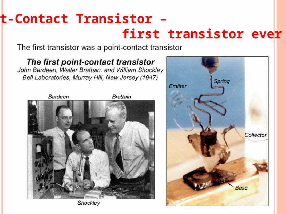
Point-Contact Transistor – first transistor ever made
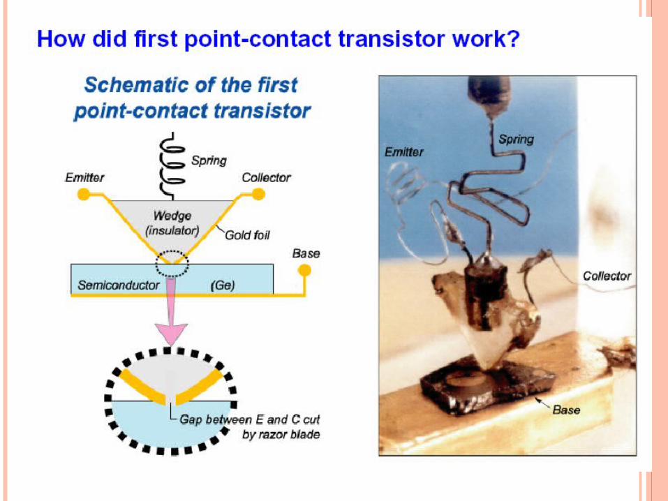

First Bipolar Junction TransistorsW. Shockley invented the p-n junction transistorThe physically relevant region is moved to the bulk of the material
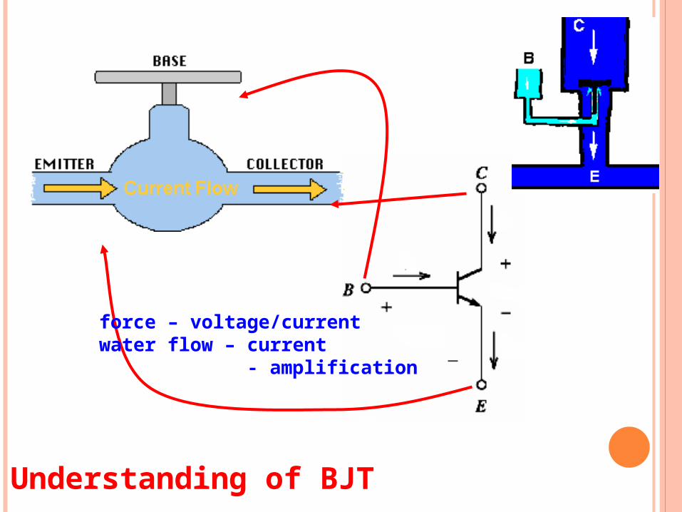
Understanding of BJT
force – voltage/currentwater flow – current - amplification
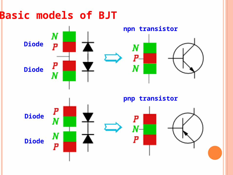
Basic models of BJT
Diode
Diode
Diode
Diode
npn transistor
pnp transistor
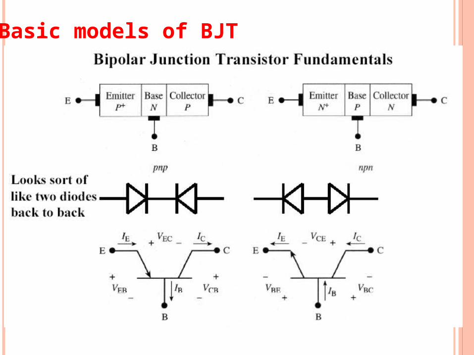
Basic models of BJT
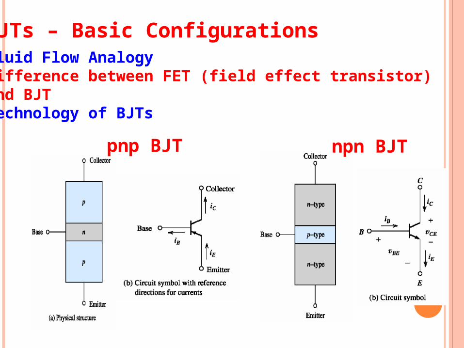
BJTs – Basic ConfigurationsFluid Flow AnalogyDifference between FET (field effect transistor) and BJTTechnology of BJTs
pnp BJT npn BJT

BJTs – Practical Aspects
Heat sink

BJTs – Testing

BJTs – Testing
RECALL P-N JUNCTION
P NWVappl > 0
-+
N PWVappl < 0
-+
Forward bias, + on P, - on N (Shrink W, Vbi)
Allow holes to jump over barrier into N region as minority carriers
Reverse bias, + on N, - on P (Expand W, Vbi)
Remove holes and electrons awayfrom depletion region
I
V
I
V

BIPOLAR JUNCTION TRANSISTORS: BASICS
+
- +
-
IE IBIC
IE = IB + IC ………(KCL)
VEC = VEB + VBC ……… (KVL)
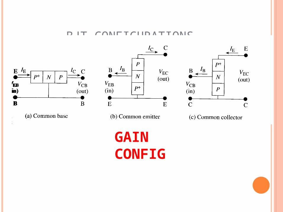
BJT CONFIGURATIONS
EC
E 6
63
GAIN CONFIG

BIPOLAR JUNCTION TRANSISTORS: BASICS
EC
E 6
63
Bias Mode E-B Junction C-B Junction
Saturation Forward Forward
Active Forward Reverse
Inverted Reverse Forward
Cutoff Reverse Reverse
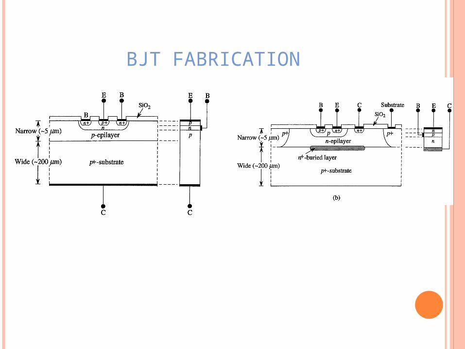
BJT FABRICATION
EC
E 6
63

PNP TRANSISTOR AMPLIFIER ACTION
EC
E 6
63
IN (small)
OUT (large)
Clearly this works in common emitterconfiguration

COMMON BASE DC CURRENT GAIN - PNP
Common Base – Active Bias mode:
EC
E 6
63
IC = DCIE + ICB0
ICp = TIEp = TIE
IC = TIE + ICn
DC = T

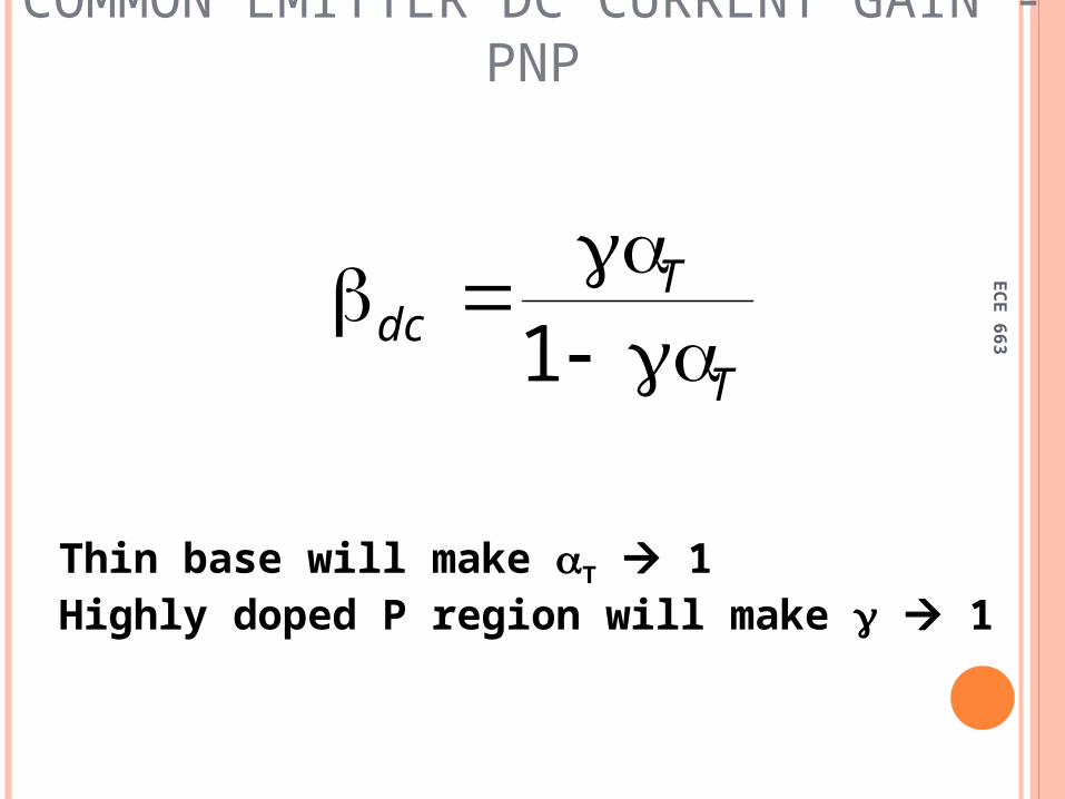
COMMON EMITTER DC CURRENT GAIN - PNP
Common Emitter – Active Bias mode:
EC
E 6
63
IE = DCIB + ICE0
DC = DC /(1-DC)
IE
IBIC
IC = DCIE + ICB0
= DC(IC + IB) + ICB0
IC = DCIB + ICB0
1-DC
GAIN !!
COMMON EMITTER DC CURRENT GAIN - PNP
EC
E 6
63
T
Tdc
1
Thin base will make T 1Highly doped P region will make 1

THAN
K YO
U