UNIVERSAL COLLEGE OF ENGG. AND TECH. ANALOG ELECTRONICS.
22
UNIVERSAL COLLEGE OF ENGG. AND TECH. ANALOG ELECTRONICS
-
Upload
holly-king -
Category
Documents
-
view
219 -
download
3
Transcript of UNIVERSAL COLLEGE OF ENGG. AND TECH. ANALOG ELECTRONICS.

UNIVERSAL COLLEGE OF ENGG. AND TECH.
ANALOG ELECTRONICS

AIM: OP-AMP AMPLIFICATION, DC AND AC AMPLIFIERS, SCALING AND SUMMING
AMPLIFIERS
Prepared By:
Group:- 12 (C)
Devansh Dave 130460109011
Parita Bhavsar 130460109007
Guided By:
Prof. Kapil Dave

FLOW OF PRESENTATION
• Op-Amp• TERMINOLOGY• 741 Op-Amp• Schematic Diagram of Op-Amp• Inverting Amplifiers• Non-Inverting Amplifiers• Summing Amplifiers• Scaling Amplifiers

OP-AMP
• Op-Amp-An active circuit element designed to perform mathematical operations of addition, subtraction, multiplication, division, differentiation and integration.
• High performance linear amplifier that requires a power source to operate.

TERMINOLOGY
• Gain- Amount of amplification produced by an Op-Amp. Gain is independent from the supply voltage (power given for the Op-Amp to operate).
• Open-Loop Mode-Function of an Op-Amp when the feedback resistor (Rf) is zero. The Op-Amp operates as a comparator and not as a linear amplifier.

TERMINOLOGY
• Comparator-Compares the –V and +V inputs to see which is greater and returns a result.
• Bandwidth-The range of frequency at which an Op-Amp will function. (Ideal = ∞)

TERMINOLOGY
• Slew Rate (V/µs)- Amount of time it takes for the Op-Amp to step to another voltage level. (Non-Ideal)
• Input Offset Voltage- Even when there is no input voltage the Op-Amp gives off a small voltage. This can be canceled out by use of the Offset Null pin on the chip. (Non-Ideal)
• Common Mode Rejection Ratio (CMRR)- Ability of an Op-Amp to reject a signal applied to both inputs simultaneously.

741 OP-AMP
Maximum Ratings
Supply Voltage ±18 VPower Dissipation 500 mWDiff. Input Voltage ±30 VInput Voltage ±15 VOperating Temperature 0°C to 70°C
Characteristics
Input Offset Voltage 2 to 6 mVInput Resistance .3 to 2 MΩCMMR 70 to 90 dBBandwidth .5 to 1.5 MHzSlew Rate .5 V/µs
1
2
3
4 5
6
7
8
-
+
- INPUT
+ INPUT
- V
Output
Offset Null
+ V
Offset Null
No Connection

Schematic Diagram of 741 OP-AMP

OP-AMP TYPES
Op-amp DC
AC
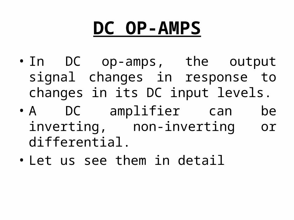
DC OP-AMPS
• In DC op-amps, the output signal changes in response to changes in its DC input levels.
• A DC amplifier can be inverting, non-inverting or differential.
• Let us see them in detail
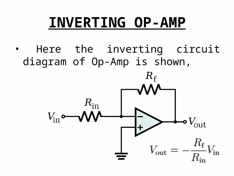
INVERTING OP-AMP
• Here the inverting circuit diagram of Op-Amp is shown,
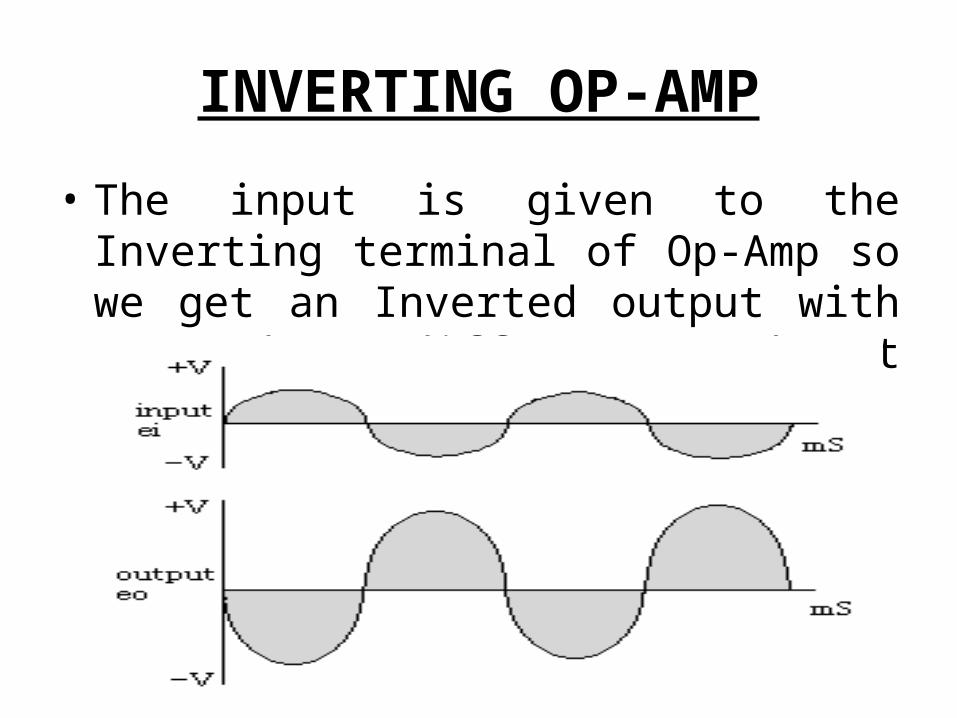
INVERTING OP-AMP
• The input is given to the Inverting terminal of Op-Amp so we get an Inverted output with 180° phase difference and out of phase.

NON-INVERTING OP-AMP

NON INVERTING AMPLIFIER
• The input signal is given to non-inverting terminal of Op-Amp. The output is without any phase difference and in phase to input.

DIFFERENTIAL AMPLIFIER
If R1 = R2 and Rf = Rg:

DIFFERENTIAL AMPLIFIER
• It amplifies the difference between two voltages but does not amplify the particular voltages.
• Where Vin+ and Vin
- are the input voltages and Ad is the differential gain

SUMMING AMPLIFIER

SUMMING AMPLIFIER@" "
a b c f
a b c out
a b c f
ff f
out a b c
a b c
KCL A
i i i i
v v v vR R R R
R R Rv v v v
R R R
@" "
a b c f
a b c out
a b c f
ff f
out a b c
a b c
KCL A
i i i i
v v v vR R R R
R R Rv v v v
R R R

SCALING AMPLIFIER

REFERENCES
• Ramakant A Gayakwad, Op-Amps and Linear integrated circuits, Prentice Hall of India
• K.R.Botkar, Integrated Circuits, Khanna Publishers
• www.google.com• www.wikipedia.org

THANK YOU