Cray XC Series Network The Cray XC series is a distributed memory ...

United States Patent ~91 1111 3,833,889 Cray 1451 Sept. 3, 1974
I.541 MULTI-MODE DATA PRO(‘ESSlNG SYSTEM
[ 751 Inventor:
[ 73 ] Assignee:
[ 221 Filed:
(211 Appl. No.
[52] U.S. Cl. [51] Int. Cl.....
Seymour R. Cray. Chippewa Falls, Wis.
Control Data Corporation, Minneapolis, Minn.
Mar. 8. 1973’
339,237
,............... 3401172.5 G06f 9/20, G06f 15/ I6
[ 581 Field of Search ._......._.. 340/l 72.5; 444/l
[561 References Cited UNITED STATES PATENTS
3,234.5 19 2/1966 Scholten 340/172.5 3.239.8 I6 311966 Breslin et al 3401172.5 3.245.047 4/1966 Blaauw et al 340/172.5 33544,965 12/1970 Packard 340/172.5 3.735,360 511973 Anderson et al 340/172.5
R26,171 311967 F‘alkoff 3401172.5
Primary E~n,,lirrPr--(;areth D. Shau Assistant Exuntitler-John P. Vandenburg Attorney, Agent. or Firm-Robert M. Angus
1571 ABSTRACT
A computer system according to the present disclo- sure includes a plurality of individual processors and an interlock register connected to the processors for process control independent of memory. One aspect of the disclosure resides in a “universal” register tech- nique and apparatus wherein the main registers of each processor are selectively operated in a plurality of modes. Another aspect of the disclosure resides in an addressing technique and apparatus wherein a ref- erence address of an object program is selectively added to addresses of programs inside and outside of the field length of the object program to obtain the ab- solute address of the program. Absolute addresses of resident programs, however, are handled by not add- ing the reference address to the resident program ad- dress.
73 Claims, 13 Drawing Figures
PROCESSOR
301 361 I I I 1 I
INPUT- TO - OUTPUT
STATION
~-:I
PERIPHERAL EQUIPMENT
371
MPINTENANCE CONTROL
MEMORY
L PROCESSOR -
337
_c PROCESSOR v
34-J

PATENTED SEf’ 3 1974 SHEIT 1 OF 7

FIG. 2A j79 ADDRESS
SHIFT CONTROL 4
761 777 NEXT INSTRUCTION ADDRESS
STATEMENT 1’ STACK ADDRESS ( 12 RANKS @ 20 BITS)
COI NCIDENCET TEST t-87
OR Y-
+I 60 I-P
86-’

L j66 __--__-- I
-73
FIG. 2B I I INTERLOCK REG. CONTROL
62 $3) L , . ,
F.l? BOOLEAN, SHIFT, /57 ARlTHMETlCS LONG ADD CONTROLS
547 MERGE NETWORKS
ACCESS CONTROL
TO FIG3 Ir 1L 50- - 126-t f&5$24 z
EXCHANGE PARAMETER
WORD ,
1 REGISTFR 1 1
c61
tt
+
_-X REGISTERS (16)
-----_w___
Ill.IIlIIlI
RA
RB
RC
RD
t
-
/68
FROM Y MEMORY E
Cal
t

PATENTRI SEP 3 1974 3,8X3.889
.-_.--- _----..- -3 __-- ii! +r Y s ii W c t

PATENTED SEf’ 3 1974 3.833.889 SHEET 5 OF 7
FROM EXCHANGE PARAMETER WORD REG. (FIG 28)
BITS 6-20 ADDRESS 1 - REGISTER 1
1 lNSTF?UCTlON 7-I SELECT FETCH
ADDRESS REGISTER lOGRAM
ADDRESS lOI/ ’
REGISTER I lO5rj l
\ +oo 7
OUT-OF-STACK . + FLAG
843 11 T
I / ). I SELECT
I FdOM COINCIDENCE TEST
(FIG 2A)
t-124 lo31 EXCHANGE i
I ho2 I 106) 1 ,
125
FROM ISSUE 1 CONTROL J+ DATA STORAGE
(FIG 2C) REF. GROUP
FROM -PO EXCHANGE PROGRAM
F!4RAMETER REF. FLAG WORD REG.
(FIG 28)
FIG. 3
BITS’ 9-20
STORAGE ADDRESS ,I 07 REGISTER
1
STORA;AT;;ZLESS 128

PATENTED SEf’ 3 1974 39833,889 SHEET 6 ff 7
256 K WORD MEMORY
r
i I
131 e : :; l-
> USER R
r LIBRARY JUMP
LIBRARY JUMP
FIG. 4
EXCHANGE PARAMETER WORD (FR. REGISTER 00)
127
EXCHANGE ADDRESS REGISTER
FIG.6 ADD;, \ ,2 , [:“N; SELECT
STORAGE ADDRESS REGISTER
FIG.7

PATENTED SO 3 1974 SHEET 7 Of 7
3;833,889
COEFFICIENT COEFFICIENT
48 1 ‘OUT-OF-RANGE
FLAG FIG.8 v xk [ 16 48 I
SIGN EXTENSION A ‘COEFFICIENT
COEFFICIENT EXPONENT SIGN, / h \
I COEFFICIENT
FIG.9 COMPLEMENT IF COMPLEMENT IF COEFFICIENT COEFFICIENT SIGN POSITIVE SIGN NEGATIVE
xi% [ 51 I 13 I SIGN EXTENSION-f CEXPONENT
x c3
X8
01
I / ,,‘/, ’ / ///, // ,,&
/ ,,/ ,’
CbkEMENT SIGN EXT BIT
EXPONENT / h
JT- OF- RANGE- /-
EXPONENT FLAG
(-COEFFICIENT

3,833,889 1
MULTI-MODE DATA PROCESSING SYSTEM
This in\,ention relates to computer systems. and par- ticularly to a multi-processor computer system utilizing an interlock control between the several processors for controlling independent processing operations of each respective processor. Additional aspects of the present invention reside in the prov,ision of universal registers capable of being used as index. program address. and arithmetic or operand registers, and in the provision ot an addressing technique useful for exchange jumps. program operation and library access.
Multi-processor computer systems are characterized by the inclusion of a plurality of individual processors connected to a common memory. Heretofore, delega- tion of processing operations, inter-processor controls, and inter-processor data transmission have been ac- complished by selectively controlling the common memory to forward data to and between the individual processors for operation thereby. Although such multi- processor computer systems have been successful, in- herent limitations have been imposed on such systems by virtue of the considerable amount of time devoted to acquiring delegation and processing instructions from the memory, and because the processed data in- tended for communication between individual proces- sors must be routed through the memory.
Heretofoie computer processors have ordinarily in- cluded a plurality of individual register sets, a first set of which are hardwired for program address purposes, a second set of which are hardwired for program ad- dress purposes, and yet another set of which are hard- wired as accumulators for arithmetic operations. Therefore, an individual processor might include as many as twenty-four registers, eight for indexing, pro- gram addressing, and accumulation purposes. Thus, only eight registers were available for each operation. Ordinarily, the registers of each type are sized in accor- dance with the requirements of each individual opera- tion. Thus, the index registers have one capacity, the address registers another capacity. and the accumula- tion registers yet another capacity.
It is an object of the present invention to provide a processor having a plurality of registers which are se- lectively operated through merge and distribution net- works to accomplish indexing, program addressing, and accumulating operations, depending upon the manner of operation of the merge and distribution networks. Thus, with “universal” registers in accordance with this aspect of the present Invention the total number of reg- isters may be reduced, and yet more registers are avail- able for any individual function.
It is yet another object of the present invention to provide a control network for selectively gating a plu- rality of registers for operation in accordance with a se- lected one of a plurality of desirable operations.
It IS yet another object of the present invention to provide a multi-processor computer system having a plurality of individual processors connected to a com- mon memory wherein interlock control mean is pro- vided to delegate processing operations to the individ- ual processors without requiring delegation informa- tion to be provided by the memory.
Another object of the present invention is to provide a multi-processor computer system wherein data to be forwarded between individual processors is routed
5
IO
I5
20
25
30
3.5
40
45
50
55
60
6.5
2 through a common Interlock control, rather than through a common memory.
Another problem associated with prior processors resides in the fact that addresses associated with a par- ticular object program bore some relationship to the physical arrangement of the memory, and in order to effectuate ,jumps or calls to program (object and/or res- ident) outside of the field length of the particular ob-
ject program. the absolute address of the program being called or jumped to first had to be retrieved from memory. Thus, upon return to the original object pro- gram. the absolute address of that program had to be also retrieved from memory.
Accordingly, it is yet another object of the present invention to provide a processor having memory access controls which contain a reference address of the oper- ating object program, the controls being selectively gated to access the memory at an absolute address (such as might be associated with a resident library rou- tine), or the reference address (such as when operating in the field of the object program), or to a modified ad- dress to affectuate jumps to programs outside of the field of the object program.
In accordance with the present invention, a plurality of processors are individually connected to a common memory as well as to an interlock control means. The interlock control means delegates processing operation to the individual processors. All input/output control, maintenance control, bulk memory and disc files are connected to the memory.
In accordance with one feature of the present inven- tion. a computer processor is provided having a plural- ity of individual registers having, as their common in- put. a merge network, and having, as their common output. a distribution network. At least one output from the distribution network is connected to memory, and at least two other outputs of the distribution net- work is provided to the merge networks. A program controller is provided for controlling access to the reg- isters through the merge networks and for controlling selection of the distribution networks in accordance with predetermined instructions so that the registers may be selectively operated as index registers, program address registers, arithmetic or accumulator registers,
or any combmation thereof. Yet another feature of the present invention resides
in a memory access control for a processor wherein a reference address relating to an object program is stored. the control having a register for storing an ex- change address and a register for storing a program ad- dress A gate is provided for selectively gating a mem- ory either the exchange address (as incremented through suitable increment circuits) or the program ad- dress combined with the reference address, the pro- gram address being incremented for successive ad- dresses.
The above and other features of this invention will be more fully understood from the following detailed de- scription and the accompanying drawings, in which:
FIG. I is a block diagram of a multi-processor com- puter system in accordance with the presently pre- ferred embodiment of the present invention;
FIGS. 2A. 2B and 2C, when edge matched as shown in FIG. 2D, form a block diagram of the register and control portions of an individual processor;

3,833,889 3 4
FIG. 3 IS a block diagram of a portion of the control elude an integer (or long) adder, a boolean control, section of an rndrviclual processor as particularly appli- and a shift control) Controls 57 receive inputs from cable for out of stack instructron access; operand register 63, and operand register 64. Operand
FIG. 4 15 a representation of a memory showing the register 63 has inputs from the instruction control via operation of an access operation; s channel 66, and from distribution network 51 via chan-
FIG. 5 1s a representation of an exchange parameter net 67. Distribution network 51 has outputs via channel word format for use in an access operation; 68 to operand register 64 and through complement cir-
FIG. 6 IS a representation of an exchange address for- cuit 69 to register 64, to floating point arithmetics 56 mat for use in the exchange parameter word; via channel 58, to interlock register 40 via channel 132,
FIG. 7 is a representation of an instruction for mem- IO and to memory 34 via channel 99. Operand register 64 ory access; and receives inputs from register designator 70, mask con-
FIGS. 8 - 10 are representations of pack and unpack troller 71 and from the instruction control via channel operations for floating point format. 73. Parameter register 62 receives inputs from inter-
DETAILED DESCRIPTION lock register 40 VI;I channel 72, from the instruction
IS control via channel 73 and from external access con- With reference to FIG. 1, there is illustrated a multi- troller 74. Suitable pack and unpack circuits (not
processor computer system in accordance with the shown) may also provide inputs to networks 53 for presently preferred embodiment of the present inven- floating point functrons obvious to one skilled in the tion. The computer system includes a plurality of indi- art. vidual processors, 30, 31, 32, 33 connected to a corn- 20 The instruction controller-, shown in FIG. 2A, has an mon memory 34. For example, memory 34 may be a input from memory 34 via channel 75 to instruction 256K-word memory, each word having 64 bits. The word stack 78. Instruction address stack 77 has an memory is connected through buffer 35 to an input- input from next statement address 76 which is incre- /output station 36, maintenance controller 37, bulk mented via positive increment controller 59. As will be memory 38 and disc files 39. Input/output station 36 is 25 more fully understood hereinafter, a single instruction preferably connected to suitable peripheral equipment address stack 77 and an instruction word may comprise such as card readers, tape drives, optical readers, read- a 64-bit word channeled to instruction word stack 78 out devices, and other suitable peripheral equipment from memory. Shift controller 79 has an input to in- welt known in the art. The input/output station, to- struction address 77 and to shift controller 80, which gether with such peripheral equipment as may accom- 30 in turn has an output to instruction word stack 78. pany it, provides the necessary raw data input and data Program address register 81 has an input from OR output for processors 30-33. Of course in large scale gate 82 which in turn has inputs from plus or minus in- operations, the input/output station may itself be a crement controller 83 and branch address 84. Incre- smaller computer. Interlock register 40 is connected to ment controller 83 receives its input from address reg- each processor 30-33. it is to be understood that al- 35 ister 81 thereby forming a loop, while branch address though four processors are illustrated in FIG. 1, there 84 has input from the RA and RB Sections of registers may be any number of processors. and that four are 50 via channels 85, 86 respectfully. Branch address 84 shown for purposes of explanation and not of limita- has a 20-bit capacity so that it receives all I6 bits from tion. Further, although bulk memory 38 and disc tiles 39 are shown connected to buffer 35, it is to be under- 4o
the RA section of any RA register of registers 50 and receives 4 bits from the corresponding RB section of
siood that in some circumstances they may be omitted. registers 50. Program address register 81 has outputs to coincidence test controller 87, to next statement ad-
With reference to FIGS. ZA, 2B and ZC, when edge dress 76 and to operand register 63 via channel 66. Co- matched as shown in FIG. 2D, there is illustrated a por- incidence test controller 87 compares the program ad- tion of a typical processor 3&33 for controlling the op- 45 dress in register 81 with the instruction address in stack eration of a plurality of registers 50. The plurality of 77, and provides control outputs to parcel control 88, registers 50 may comprise 16 individual registers desig- rank control 89 and out-of-stack flag 100. Rank con- nated 00 through 15, inclusive, each having a 64-bit ca- troller 89 provides suitable gate signals to AND gates pacity. Also, and as shown particularly in FIG. ZB, the registers may be geometrically divided into four sec-
5. 90 to control transfer of instruction words from instruc- tton word stack 78 to current instruction word register
tions designated RA. RB. RC and RD. inclusive, each 91. Parcel controller 88. which is incremented by posi- having a capacity of I6 bits. Thus, for any individual tive increment controller- 60, provides suitable gate sig- register. the first 16 bits will be placed in the RA sec- nals to AND gates 92 and 93 to control transfer of bits tion, bits I7 through 32 vvill be placed in the RB sec- tion, bits 33 through 48 wilt be placed in the RC section
55 to translator 94 and to program register 95, respec- ttvely. Translator 94 provides an output to access con-
and bits 49 through 64 will be placed in the RD section. troller 54 and selection controller 55 via channel 120 Each register 00 through 15 has an output to distribu- while program register 95 provides an output via chan- tion network 51. Also, each register has an input nel 73 to parameter register 62. Translator 94 receives through a plurality of AND gates 52 from merge net- 6. a I h-bit instruction parcel from register 9 1, while regis- work 53. AND gates 52 are selectively controlled by ter 95 may receive I6 hits of a 20-bit program code access control 54 which :n turn is controlled by the in- from register 91. As will he more fully understood here- struction control shown generally in FIG. 2A. inafter, if a program code is to be transferred to register
Merge network 53 has, as inputs thereto, inputs from 95, the other four bits of the 20-bit program code will floating point arithmetics 56 (which might include a 65 be supplied from translator 94. floating point divider, floating point multiplier and Translator 94 also provides an output via channel floating point adder), memory 34 via channel 65, pa- 121 to issue controller 122, which in turn provides an rameter register 62, and controls 57 (which might in- output to data storage reference group 111 (FIG. 3) via

3,833,889 5 6
channel 123, and It provides set and clear signals to in channels 85 and 86. The Instruction address might, for terlock regrsler 40. example. comprise 20 bits while the instruction word
Exchange par-ameter word r-egrstcr 61 is connected to mrpht comprise 64 hrts As will be more fully under- the output of 00 register SO to receive the entire 64hit stcxrd hereinafter, I( IS the instruction address that lo- word contained therem Register 61 is adapted to pro- 5 cates ;I particular instruction word for operation. The vide ;I 2O-bit program address code via channels 8.5 and instructron addresses are stored in instruction address 86 to branch address 84, an X-bit exchange address stack OI- register 77 and the instruction words are code via channel 124, a I2-bit reference address code stored 111 instruction word stack or register 78. By way via channel 125 and a program reference flag bit \,ia of example. stack 77 may be capable of storing up to channel 126. IO twelve addresses, and stack 78 may be capable of stor-
FIG. 3 illustrates a block logic diagram of circuitry ing up to I2 64.bit words. assoctated with the instruction address and word mod
ules for acquiring instruction words from memory As Assumrng that a proper instruction address and its shown in FIG. 3, program address register 81 has out- associated instruction word are stored in stacks 77 and puts to select circuits 101 and 102. Exchange address 1.S 78, and that the RA and RB sections of X register 50 register 103 has two outputs, one to select circuit 101 ha1.c been conditioned to cause that instruction to con- and another to adder 104. Exchange address register 103 has a ZO-bit capacity such that the first five bits are
trol some processing operation (e.g. addressing, index- ing or arithmetic), a 20-bit code is forwarded via chan-
forwarded to adder 104 while the last 15 bits are for- nels 85 and 86 to branch address 84. Branch address 84 warded to select circuit 101. The first five bits are also 20 receives the entire l6-bit RA portion of the condi- recycled through positive increment controller 127 tioned one of the 16 X registers, as well as the first four thereby forming a counter. Select circuit 101 has an bits from the corresponding RB portion. This 20-bit output to instruction fetch address register 105. Select circuits 101 and 102 have further enable inputs from
code is forwarded through OR gate 82 to program ad- dress register 81. The 20-bit address is forwarded to co-
out-of-stack flag 100. 25 incidence tester 87 and to next statement address 76 Instruction fetch address register 105 has a first out- which operates on stack 77 to locate the particular ad-
put to increment adder 114 which adds binary I to the dress therein. If the proper address is present in stack contents of register 105 and forwards the result to se- lect circuit*lOl. A second output from register 105 for-
77, coincidence tester 87 determines the coincidence between the addresses in register 81 and stack 77, and
wards the IS most significant bits contained therein to 3” forwards a control signal to rank controller 89. Rank adder 104 for combination with the five least signifi- controller 89 provides a gate output to AND gates 90 cant bits from register 103 for forwarding to select cir- so that the corresponding word in stack 78 is forwarded cuit 102. A thrid output from register 105 provides for to current instruction word register 91. transfer of the contents (20 bits) of the register directly If the designated instruction address is not condi- to select circuit 102. j5 tioned for immediate output to coincidence test 87, no
Select circuit 106 receives one input from select cir- coincidence IS determined by tester 87, and shift con- cuit 102 and a second from branch address 84 (which m turn receives a 20.bit input from the RA and RB por-
troller 79 will step stack 77 to sequentially provide other addresses in stack 77 until a coincidence is deter-
tions of registers SO--FIG. 2B). Thus, select circuit 106 mined in tester 87. Simultaneously shift controller 79 will transfer a 20.bit code, whether received from ‘” controls shift controller 80 to correspondingly step the branch address 84 or received from select circuit 102. rnstruction words stored in stack 78 so that when a co-
incidence IS determined in tester 87, the proper current The eight least significant bits from select circuit 106 instruction word is located at the output of stack 78.
are transferred directly to storage address register 107 Rank controller 89, when operated by tester 87, con-
for operation on the storage access control 128 associ- ” ditions stack 78 to transfer the current instruction word ated with memory 34 via channel 129. The 12 most sig- from stack 78 to current instruction word register 91. nificant hots from select circuit 106 are forwarded to adder 108 where they are binarily added to the output It should be recogmzed that any instruction address from AND gate 109 and the result is forwarded to reg- 5. contained in stack 77 may be accessed. Thus, incre- ister 107 as the 12 most significant bits therein. ment circuit 83 is capable of selectively incrementing
Program reference flag 110 and data storage refer- both positive and negative so the addresses may be ence group 111, which receive inputs from register 61 gathered sequentially in either ascending or decending and control 122, respectively. provide gate signals to order. OR gate 112 which rn turn provides a gate signal to 5 AND gate 109. Reference address register 113 pro- ’ The Instructron words stored in memory, in stack 78 vides a l2-bit reference address from register 61, which and in register 91 are 64.bit words containing four l6- when gated by AND gate 109, is added to the 12 most brt parcels. A single mstruction may comprise one or significant bits from select circuit 106 for transfer to two parcels ( I6 or 32 bits). A one parcel instruction register 107 as the I2 most significant bits therein. h,, will consist of a 4, 6 or g-bit instruction code and one
OPERATION .“’ or more designator codes which will control operation
of access and/or selection controllers 54 and 55. A two With reference to FIGS. 2A, 2B and 2C, which taken parcel instruction will consist of a 4 to g-bit instrustion
together as shown in FIG. 2D, illustrate a block circuit diagram of the control portions of an individual proces-
code, a designator code or codes, and a 20-bit program
sor 30-33, an instruction word is received from mem- 6s code for destination to parameter register 62 and/or
operand register 64. ory 34 by instruction word stack 78 via channel 75, and As will be more fully understood hereinafter, the X an instruction address is received from registers 50 via registers 50 are controlled for a selected one of plural-

3,833,889 7 8
ity of condltlons, I e. internal transfer. output to oper- registers. or any of them , are entry and resultant oper- and regl5ter 03, output to opcr:uid register 64, output and register\ For ex;tmplc. an instruction code (F)
to interlock rcplster 40, output to the bloating pollIt which dictatc5 ;&Jltion of the contents of the Xi and arithmetic units. and output to memory. These outputs Xk registers will cause those registers identified by the are controlled hy the instruction code and the designa- s i and k designators to be entry operand registers. If the
tor codes. In the case of a one parcel instruction, the same instruction code (F) dictates that the addition re- parcel will have one of the following formats: sult (formed by the long add 57 or the floating point
arithmetics 56) be forwarded to the Xj register, the re- (,,.... ~.m sulting computation is forwarded to that register identi-
IO tied by the j designator to be the resultant operand reg- ister. Thus, the entry and resultant functions are dic-
(ii)...-. mi tated by the instruction code, and not necessarily by the designator. Obviously, any of the Xi, Xj and Xk reg-
-___ isters may be entry or resultant operational registers, 15 depending upon the particular instruction and upon
(CL.. f++$ later use of the information. For further elaboration of the format of the instruction words, reference may be had to Pat. No 3.346.851 granted Oct. 10, 1967 to
where F is the instruction code, i,j and k are designator James E. Thornton and Seymour R. Cray for “Simulta- codes for operand source and destination, and n is a 20 neous Multiprocessing Computer System”, and partic- constant. In the case of a two parcel instruction, the ularly to column 7 et seq. thereof, but care should be one of the following formats is available. taken in referring thereto in as much as the operation
of the processor on the instruction words therein differs
y-; / : j : / “, from the prcscnt invention at least to the cxtcnt tic- 25 scribed herein.
A rcxc-rv:ltlcul 11;1g I\ 1~toviclcd li)r each of the I6 X rcgihtcrh 50. Whcli s;c’l. 111~. Il;lg\ Ic’liiain set until spcciti-
(VJ..../ : / :I / L tally cleared. When translator 94 issues an instruction containing a designator (i, j and/or k) which designates
30 a particular X register as the destination registe,r, the X where K is a 20-bit program code for parameter regis- reservation flag for that register is set in a manner dic- ter 62 and/or operand register 64. tated by the designator. Translator 94 examines the in-
Thus, in case i, the instruction will consist of a 4-bit struction code of each instruction to determine the in- instruction code, a 4-bit i designator. a 4-bit j designa- btruction (or control function) and examines the i, j tor and a 4-bit k designator. In case ii the instruction 35 and k designators to determine which of t$ I6 X regis- will consist of a 6-bit instruction code, a 2-bit constant, ters is to be operated and in what manner. a 4-bit j designator and a 4-bit constant. In case iii the For example, assume it is desirable to read informa- instruction will consist of an g-bit instruction code, a tion from X register 08 which carries a k designator 4-bitj designator and a 4-bit X designator. In case iv the (Xk of register 08) and copy that information into reg- instruction will consist of a 4-bit instruction code. a 40 ister 12 to carry a j designator (Xj of register 12). The 4-bit i designator, a 4-bit j designator and a 20-bit pro- instruction may consist of a one parcel instruction in gram code. In case v the instruction will consist of an the form of case iii whose instruction code (F) instructs g-bit instruction code, a 4-bit j designator and a 20-bit a read operation from some Xk register via channel 68 program code. It is noteworthy that in each case the in- to operand register 64 and thereafter write the data struction code occupies the first 4, 6 or g-bit positions, 45 into some Xj register. The specific Xk and Xj registers the i deisgnator occupies the second 4-bit positions (in are determined from the k and j designators, respec- the case of 4-bit instruction codes only), the j designa- tively. tor occupies the third 4-bit positions, the k designator As another example, assume it is desirable to read in- occupies the fourth 4-bit positions (in the case of one formation from register 08 which carries the j designa- parcel instructions onfy,) and the program code consists “’ tor, add some program code (K) to it, and copy the re- of the last 20-bit positions (in two parcel instructions sult into register 12 carrying an i designator. In this case
.m only ). the instruction will consist of two parcels in the form of X registers 50 comprise 16 64-bit registers. Each case iv whose instruction code instructs a read opera-
piece of information, whether data or instructional, is tion from some X,/ register to operand register 63, a accompanied by one or more designators (e.g.. i, j or 55 transfer of the program code (K) to operand register k). This designator is determined either by register des- 64, an addition of the data in registers 63 and 64 by ignator 70 or from the designator codes contained in long add controls 57, and writing the result into some the instruction words. The designators are not ad- Xi register. The specific Xi and Xj registers are deter- dresses which determine the location of storage of in- mined from the i and j designators, and the value of K formation. but instead are merely designators to enable ‘() IS carried with the instruction as the 20.bit program retrieval of the informatIon in a predetermined man- code in register 95. ner. Thus, as used hereinafter. the terms Xi, Xj and X/i. MERGE AND DISTRIBUTION NETWORKS when denoting a part. or used in connection with, X The merge networks 53 and distribution networks 51 registers 50, merely means those registers or portions 65 a,re static logic switching networks responsive to gate of registers which are to receive information, or from stgnals to selectively access selected ones of registers which information is to be gathered, as the case may 50. As is more fully explained elsewhere herein, in- be. structions issued from translator 94 includes 4-bit des-
Each instruction carries with It a 4.6 or g-bit instruc- ignator codes (designated i. j and k). As will be more tion code (F) which dictates which of the Xi, Xj or Xk fully understood hereinafter, the i, j and k designators

3,833,889 9 10
arc used to desrgnatc particular rcglstcrs from which ncousi~ steppmg by one through increment circuit 60. and/or to which data is directed. .Thc d-hit designator After the li~st Instruction issues, parcel controller again codes operate on the logical switching netwc~rh:, of the IS ~ncrnmzntetl by one through increment circuit 60 to merge (fun-in 1 and iiistributlan (fan-out) networks to gam acceh~, to the second (or third) parcel. The process selcctlvety gate the data to and from the selected regis- 5 continues until the complete word is read. ters. The exact nature of these networks a~-c apparent It may he necessary in certain circumstances to issue to one of ordinary skill in the art, given the fact that the a parcel pass control to complete a 64-bit instruction designator codes, together with the instructions selec- word. .Ihis IS done to avoid starting a two parcel in- tively operate them. For example an instruction “Float- struction in the fourth parcel of an instruction word. ing Single Precision Multiply Of Xj Times Xk to Xi” IO OU f-OFSTACK INSTRUCTIONS wilt contain an instruction code (F) and i,j and h desig- Situations may arise wherein instruction words in- nators. The four bit J and k codes are issued by transta- tended for translator 94 (and register 95 in the case of tor 94 to distribution network 51 to operate logical two parcel instructions) are not contained in instruc- gates to select two registers (designated by the j and k tion word stack 78. Such a condition can occur in jump designators) and to forward the data therefrom via I5 instructions wherein a current program sequence is ter- channel 58 to the floating point arithmetic 56 (actually minated and a new sequence is commenced. Assume to the multiply circuits therein). The four bit i designa- that such a jump instruction consists of two parcels and tor is forwarded to gate 52 (which is representative of is forwarded to translator 94 and register 95. The jump the logical merge gates) to select a register (designated instruction ( I6 bits) is forwarded to control 52 via ac- by the i designator) to which the result from floating 20 cess control 54 from translator 94. Simultaneously, a point arithmetics 56 is to be stored. Other aspects of 20-bit K code, whose value is dependent upon the num- merge and distribution networks 51 and 53 will be ber of steps to be jumped, is forwarded from register 95 more readily understood from elsewhere herein, partic- to operand register 64 via channel 73. Also, the current utarly from the examples set forth hereinafter. instruction address (P) is forwarded from program ad-
25 dress register 81 (FIG. 2A) to operand register 63 As heretofor PARCEL C0NTRoL I ~-__..-.. u v~-~~t mstructton word (FIG. 2B). Integer adder 57 is operated to add the jump
consists of four I6-bit parcels. one or two of which may value K to the current address P and forward the result comprise an instruction. Thus, the t6-bit parcels, one to the RA AND RB sections of X registers 50 for trans- or two of which may comprise an instruction. Thus, the ferrat to program address register 81 via channels 85 permissible combinations of parcels comprising any 30 and 86, b ranch address 84 and OR gate 82. particular word are: If the new (jumped) address corresponds to one in
instruction address stack 77, shift controller 79 oper-
(‘)-----m 16 1 16 1 16 1 ates to shift the stack to the corresponding address until coincidence is detected in tester 87. Similarly, the in-
mu-- pi-j-TJ 35 struction word stack 78 is also shifted in the corre-
sponding instruction word for operation as heretofore described. Intermediate addresses in stack 77 and
(cl-.--~/ 16 j 32 ( I6 / words in stack 78 are discarded.
If. however, the new (jumped) address does not cor- ‘() respond to an address in stack 77, no coincidence is de-
(‘)--~--I 16 1 16 1 32 1 tected by tester 87. Instead, coincidence tester sets out- of-stack flag 100 for operation on select circuits 101 and 102 (See FIG. 3). The new address (P + K) is
(“---~~i.;3 / 16 1 16 / transferred to instruction fetch address register 105 via ” select clrcult 101, to select circuit 106 via select circuit
102, and to ne‘rt stack address 76. The 12 most signifi- Parcel controller 88 receives an input from the current cant bits of the new address (P + K) are transferred to address (via coincidence tester 87) to control which, adder 108 where a program reference flag from flag and how many. parcels of the current instruction word so 110 and exchange parameter word register 61 (FIG. shall be used to form an instruction. If the instruction 2B) is added to the new address (via OR gate 112 and comprises one parcel, parcel controller 88 selects that AND gate 109). The reference flag is transferred to parcel from current instruction word register 91 and storage address I-egister 107 for operation on the stor- gates AND gate 92 to cause the selected t6-bit parcel age access control 128 associated with memory 34. to be transferred to translator 94. If the instruction is s5 Thereafter, bits l-8 of the address are transferred from a two parcel instruction, parcel controller selects the select circuit 106 to register 107. two parcels from current instruction word register 91 As WIII be more fully understood hereinafter from the and gates AND gates 92 and 93 to cause the 12-bit in- section entitled “Exchange Jumps,” exchange parame- struction and the first four bits of the program constant ter word register contains a reference address of the to be transferred to translator 94 and the last I6-bits of 6. object program (that IS, an address of memory 34 the program constant to be transferred to program reg- wherem the object program is stored). The reference ister 95. The first 4 hirs !,f the program constant are address. which IS unique to the object program, is then transferred from translator 94 to register 95. added to the I2 most significant bits of the address for-
In operation, when a current instruction word is first warded from select circuit 106 for operation on storage presented to register 91, parcel controller 88 operates hs access control 128. to transfer the first parcel thereof to translator 94, and, The new address is thereafter transferred from next if the first parcel is part of a two parcel instruction, to stack address 76 to the twelfth rank of instruction word transfer the second parcel to register 95 while simulta- stack 77 and the instl-uction word, retrieved from mem-

3,833,889 11 12
ory 34, is placed In Instruction word stack 78 via chan- warded to storage access control 128 to enable the in- nel 75 (FIG. 2A) struction words of the library routine to be forwarded
Co~nc~dcncc tcstcr 87 now note\ the coincidence be- to instructron WOI-d stack 78 in sequence. The library tween the new address In register 81 and the new ad- address rn next statement address 76 is also incre- drcs\ in stack 77 and issues rank and parcel control s mented by rncrement crrcuit 114, and the library ad- commands to permit the new instruction to be trans- dress in program address register 81 is incremented by ferred to current rnstruction word register 91 for opera- increment circuit 83. Consequently, a coincidence will tion as heretofore described. occur in coincrdence tester 87, thereby removing the
Only a single instruction is transferred from memory out-of-stack Bag 100 and operating rank controller 89 to the instruction word stack by the foregoing method. I() and parcel controller 88 to issue library instructions, However. if it is desired to bring up a group of instruc- One feature of the absolute library address technique trons, the instruction fetch address register is incre- resides in the fact that several of the processors can si- mented through adder 114 causing an entire group of multaneously gam access to the same library routine. In instruction words to be transferred from memory to in- this respect two or more processors can gain access to struction word stack 78. Simultaneously, program ad- IS a particular libr-ary routine by issuing the absolute ad- dress register 81 is incremented through increment cir- dress of the library routine so that each receives in- cuit 83 (FIG. 2A) to permit the corresponding ad- struction words from the lihrary. Thus, and as shown in dresses to be inserted into instruction address stack 77. FIG. 4, user R having a field length FLR and a library
LIBRARY CALLS call instruction at 130 can jump to the library field at
20 131, and user T having a field length FLT and a library It may he desirable in certain circumstances to cause call instruction 133 can jump to the same library field
a jump to a portion of memory 34 containing a library 131. routine available for use by all processors. For exam- EXCHANGE JUMPS ple, and with reference to FIG. 4, assume user R is op- It may be desirable in certain circumstances to ac- erating on an object program having an address (with 25 quire data entirely from a location outside the field reference to memory 34) which commences at RAx length of an object program. For example, upon com- and has a field length FLR. Assume further that the ob- pletion of one ob,ject program, a processor may wish to ject program contains an instruction located at 130 jump to another object program. which instructs the processor to jump to a resident li- In this case, a two parcel exchange instruction issues brary routine contained in memory 34, outside of the 3. from translator 94 to transfer a program code (K) to object program field at 131. A library call instruction operand register 64 and to transfer the exchange pro- issued by the object program causes access to the resi- gram address to operand register 63. The instruction dent library routine. address stack 77 is cleared and any instruction fetches
In this case, a two parcel library call instruction issues sought by the controls in FIG. 3 are aborted. Out-of- from translator 94 to transfer a program code (K) corn- 35 stack flag 100 is set (because no coincidence can be de- prising the absolute library address to operand register tected by tester 87 due to the cleared condition of stack 64 (FIG. 2B) and to transfer the instruction address 77). thereby gating select circuits 101 and 102 to re- from register 81 (FIG. 2A) to operand register 63 ceive addresses. The exchange jump address is gener- (FIG. 2B). The instruction address stack 77 is cleared ated by the long add controls 57 (program address + K) and any instruction fetches sought by the controls 4o and is transferred to program address register 81 via X shown in FIG. 3 are aborted. Out-of-stack flag 100 is registers 50 and channels 85 and 86, as heretofore ex- set (because no coincidence can be detected in tester plained. The exchange address issues through storage 87), thereby gating select circuits 101 and 102 (FIG. 3) access control 128 as heretofore explained, causing the to receive addresses. The library address (K) is gener- contents of the exchange package to be entered into X ated through long add controls 57 and is transferred to 4s registers SO from memory via channel 65 and merge program address register 81 via X registers 50 and networks 53. channels 85 and 86, as heretofore explained. The li- The exchange package consists of sixteen 64-bit data brary address in register 81 is then transferred to in- words and one 64-bit exchange parameter word. The struction fetch address register 105 and to next state- so exchange parameter word of the exchange package ment address 76. The address issues through storage moves first. followed by exchange data words for the 00 access control 128 in the manner heretofore described, through 15 X registers rn sequence. The exchange pa- causing access to the portion of memory 34 associated rameter word, arrivmg first, is temporarily stored in the with the library address (m this case to the library field 00 X register and. one clock period later is transferred indicated at 131 in FIG. 4). It should be noted that nei-
5.5 into exchange parameter word register 61. The ex-
ther the program reference flag nor the data storage change data words till the 00 through 15 registers in se- reference group brt is set so the object program refer- quence. ence address in register 113 is not added to the library The format of the exchange parameter word is shown address. Consequently, only the absolute address of the in FIG. 5 and consists of a 20-bit program address, a library routine is transferred to storage access control 6. I2-bit field length code (indicative of the length of the 128, and the processor is conditioned to operate in the exchange package) an X-bit exchange address (corre- field of the library. sponding to K. the address of the exchange), a 12-bit
Library instructions are thereafter forwarded via reference address (corresponding to the address of the channel 75 to instruction word stack 78 (FIG. 2A) for object program-RA), an X-bit condition code and a operation in the processor. 65 4-bit mode control code. As shown particularly in
The library address in instruction fetch address regis- FIGS. 2B. 3 and 5, the 20-bit program address of the ter 105 (FIG. 3) is incremented through increment cir- exchange parameter word is transferred to program ad- cuit 114 so successive addresses of the library are for- dress register 81 via channels 85 and 86 and branch ad-
3,833,889 13 14
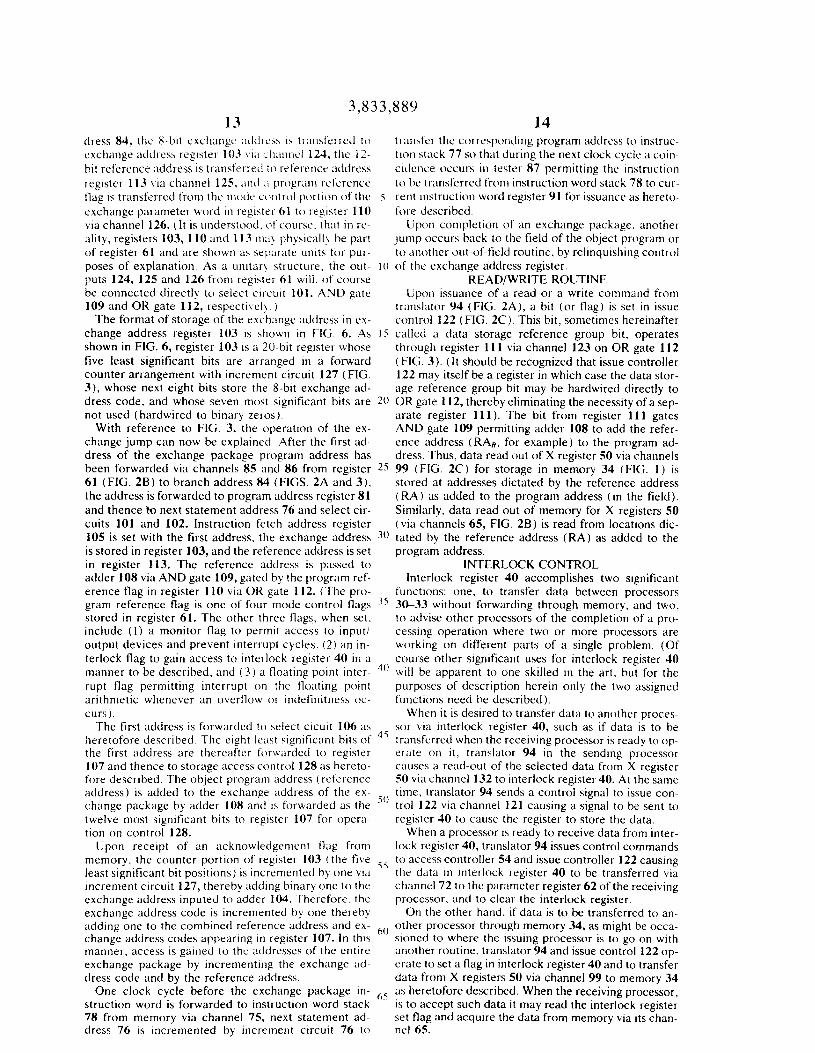
dress 84, the g-bit exchanpc ;lddi-CSx is tl~ansferrd to tr-ansfer the corresponding program address to mstruc- exchange address register 10.3 \ ia ~ti:innel 124, the 1 ?- lion stack 77 so that during the next clock cycle a coin bit reference address is transferred to reference address cidcnce occurs in tester 87 permitting the mstruction r-egister 113 vl;i channel 125, anti .i prcrpr;irn r-cferencc to be transferred from instruction word stack 78 to cur- flag is transferred from the mode contrail portrcjn of the 5 rent mstruction word register 91 for issuance as hereto- exchange parameter word in r-egrstrr 61 to register 110 fore described. via channel 126. (It is understood. c>fcourse. that in re- Upon completion of an exchange package. another ality, registers 103, 110 and 113 may physically he part jump occurs back to the field of the object program or of register 61 and are shown as sepLuate umts for pur- to another out-of-field routine, by relinquishing control poses of explanation. As a unitary structure, the out- IO of the exchange address register. puts 124, 125 and 126 from register 61 will. of course READ/WRITE ROUTINE be connected directly to select circurt 101. AND gate Upon issuance of a read or a write command from 109 and OR gate 112, respectively ) translator 94 (FIG. 2A), a bit (or flag) is set in issue
The format of storage of the exchange address in ex- control 122 (FIG. 2C). This bit, sometimes hereinafter change address register 103 IS shown in FIG. 6. As 15 called a data storage reference group bit, operates shown in FIG. 6, register 103 is a IO-bit register whose through register 111 via channel 123 on OR gate 112 five least significant bits are arranged in a forward (FIG. 3). (It should be recognized that issue controller counter arrangement with increment circuit 127 (FIG. 122 may itself be a register in which case the data stor- 3). whose next eight bits store the g-bit exchange ad- age reference group bit may be hardwired directly to dress code. and whose seven most significant bits are 20 OR gate 112, thereby eliminating the necessity of a sep- not used (hardwired to binary zeros). arate register 111). The bit from register 111 gates
With reference to FIG. 3, the operation of the ex- AND gate 109 permitting adder 108 to add the refer- change jump can now be explained After the first ad- ence address ( RAR, for example) to the program ad- dress of the exchange package program address has dress. Thus, data read out of X register 50 via channels been forwarded via channels 85 and 86 from register 2.5 99 (FIG. 2C) for storage in memory 34 (FIG. 1) is 61 (FIG. 2B) to branch address 84 (FIGS. 2A and 3). stored at addresses dictated by the reference address the address is forwarded to program address register 8 1 (RA) as added to the program address (in the field). and thence to next statement address 76 and select cir- Similarly, data read out of memory for X registers 50 cuits 101 and 102. Instruction fetch address register (via channels 65, FIG. 2B) is read from locations dic- 105 is set with the first address. the exchange address j() tated by the reference address (RA) as added to the is stored in register 103, and the reference address is set program address. in register 113. The reference address is passed to INTERLOCK CONTROL adder 108 via AND gate 109, gated by the program ref- Interlock register 40 accomplishes two significant erence flag in register 110 via OR gate 1 12. (The pro- functions: one, to transfer data between processors gram reference flag is one of four mode control flags js 30-33 without forwarding through memory, and two, stored in register 61. The other three flags, when set. to advise other processors of the completion of a pro- include (I) a monitor flag to permit access to input/ cessing operation where two or more processors are output devices and prevent interrupt cycles. (2) an in- working on different parts of a single problem. (Of terlock flag to gain access to interlock register 40 in a manner to be described, and (3) a floating point inter- 40
course other significant uses for interlock register 40 will be apparent to one skilled in the art. but for the
rupt flag permitting interrupt on the floating point purposes of description herein only the two assigned arithmetic whenever an overflow or indefinitness oc- functions need be described). curs).
The first address is forwarded to select crcurt 106 as heretofore described. The eight least significant bits of ” the first address are thereafter forwarded to register 107 and thence to storage access control 128 as hereto-
fore described. The object program address (reference address) is added to the exchange address of the ex- change package by adder 108 and is forwarded as the
so
twelve most significant bits to register 107 for opera- tion on control 128.
Upon receipt of an acknowledgement flag from memory, the counter portion of register 103 (the five least significant bit positions) is incremented by one vur increment circuit 127, thereby adding binary one to the exchange address inputed to adder 104. Therefore, the exchange address code is incremented by one thereby adding one to the combined reference address and ex- change address codes appearing m register 107. In thrs manner, access is gained to the addresses of the entire exchange package by incrementing the exchange ad- dress code and by the reference address.
One clock cycle before the exchange package in- struction word is forwarded to instruction word stack 78 from memory via channel 75, next statement ad- dress 76 IS incremented by increment circuit 76 to
When it is desired to transfer data to another proces- sor via interlock register 40, such as if data is to be transferred when the receiving processor is ready to op- er-ate on it, translator 94 in the sending processor causes a read-out of the selected data from X register SO via channel 132 to interlock register 40. At the same time. translator 94 sends a control signal to issue con- trol 122 via channel 121 causing a signal to be sent to register 40 to cause the register to store the data.
When a processor is ready to receive data from inter- lock register 40, translator 94 issues control commands
55 to access controller 54 and issue controller 122 causing the data m interlock register 40 to be transferred via channel 72 to the parameter register 62 of the receiving processor, and to clear the interlock register.
On the other hand, if data is to be transferred to an- ho other processor through memory 34, as might be occa-
stoned to where the issuing processor is to go on with another routine, translator 94 and issue control 122 op- erate to set a flag in interlock register 40 and to transfer data from X registers 50 via channel 99 to memory 34
hs as heretofore described. When the receiving processor, IS to accept such data it may read the interlock register set flag and acquire the data from memory via its chan- nel 65.

3,8: 15
MEMOK\I’ AC‘C‘ESS As heretc>fore descrrbed, \tor,rge address register 107
receives a 20-bit address from adder 108 and select cir- cuit 106 ( FIG. 3 ). Also as heretofore described, the eight least srgniticant bits of the 20.brt code are derived from one of three sources. ( I ) the program address (from either branch address 8-I to select circuit 106 or from program address register 8 I to select circuit 102 to select crrcurt 106), (2) the instruction fetch address from register 105 as incremented through increment circuit 114 and forwarded to select circuit 106 via se- lect circuit 102, and (3 ) the I s-bit exchange address from register 103 through select circuit 101 and regis- ter 105, and the 5 bits from counter section as incre- mented by increment circuit 127 and added the l5-bit exchange address by adder 104. Also as heretofore de- scribed, the twelve most srgnrficant bits of the 20-bit code are derived from select circuit 106 (via any one of the three forgomg processes) as added to the refer- ence address by adder 108 when AND gate 109 is gated by either the program reference flag 110 or the data storage reference group brt 111. Consequently, it is evi- dent that the reference address of the object program affects only the I2 most significant bits of the contents of storage address register 107; the eight least signifi- cant bits being derived from one of the three sources as heretofore described.
As shown in FIG. 7, the six least significant bits of the address code (constituting the six least significant of the eight least significant bits) control bank select in memory 34. The next I2 bits (constituting the two most significant of the eight least significant bits and the IO least significant of the 12 most significant bits) dictate the address location in a selected memory bank.
Memory 34 may consist of 64, 4K word memory banks. The 6-bit bank select code selects a particular bank while the l2-bit address code selects a particular word from that bank. As heretofore described. the least significant bits are sequentially stepped for sequential instruction words. Thus, each successive address is stepped to the next bank. rather than to the next ad- dress in a single bank This technique has the effect of sequentially stepping through the banks for the succes- sive instruction words, so that the liklihood that any one of the 64 banks becomes overloaded by requests becomes statistically small
Although the storage access control signal consists of the I8 Icast significant bits of the 20.bit code in register 107 with the upper two bits not being used, these upper
bits may be used in the case of LIII expanded memory for selectrng which, of up to four 256K word memories are accessed. Thus, with the addition of three addi- tional memories. it is possible to expand the memory to as much as 1024 K words (about 65.5 million bits).
EXAMPLES The regrsters 50 are accessible by the programmer-
operator through the input/output controls and mem- ory 34 to program data and instructions into the com- puter for computational operations. In order to explain the universal aspects of registers SO, and particularly how they function in drtferent operational modes, the following examples are set forth. It should be remem- bered, at this point, that many of the addressing capa- bilities have already been described, particularly in connection with the RA and RB portion-s of registers SO and the exchange parameter word register 61.
ARITHMETIC OPERATIONS
33,889 16
I. Logical Product of Xj and Xk to XJ - This instruc- tion causes operands to be read from the registers des- ignated by the j and X designators to operand registers 63 and 64. ‘The operands are then manrpulated by the
5 Boolean and shift circuits with the result entered into the register designated by the j designator. After trans- lator 94 issues the instruction and the.; and k designa- tors are forwarded to register 50 and the j destination register flag IS set, the data in the XJ and Xk registers
IO is read out and the reservation flag IS cleared. During the next clock period. the logical product of the con- trols of the X.1 and XX- register is forwarded back to the Xj register-.
2. Logical sum of Xj plus Xk to XJ - -This is similar IS to case 1, except the Boolean add circuits are used.
3. Logical difference of Xj minus Xk to Xj - This is similar to the cases 1 and 2, except the Boolean sub- tract circuits are used. in cases I and 2, if the j and k designators designate the same entry register, the 64 bit
20 word is merely read out of the register and thereafter re-entered into the same register. In case 3, however, if the; and k designators are the same, a 64 bit word containing all O’s is written into the register.
4. Floating Double Precision Sum or Difference of Xj 25 and xk to Xj - In these cases the data in the desig-
nated Xj and Xk registers are read into the floating point add module 56 where they are added. The details of addition are not important to an understanding of
30 the present invention, but suffice it to say that the upper half result is normalized while the lower half re- sult is not. The lower half is entered into the register designated by the j designator. For subtract operations, the subtrahend (Xk data) is first complemented and is added to the minuend (Xj data) in a manner well
35 known in the art. Double precision is ther&fter accom- plished by a single precision floating sum or difference of Xj and XX- to Xi (case 5).
5. Floating Single Precision Sum Or Difference of Xj and Xk to Xi - In this case the upper half result from
4o case 4 is entered into the register designated by the i designator.
6. Floating Divide of Xj by XX to Xj - In this case the operands from the registers designated by the j and k designators are forwarded to the floating point divide
” module 56 to form 21 quotient which is transmitted to the register desrgnated byj. The remainder from the di- vision process is discarded. If the division operand is not normalized. the out-of-range flag is set.
so 7. Floating Double Precision Product of Xj Times X/i
to Xj - In this case two normalized floating point oper- ands from the regrstcrs designated by the j and X desig- nators are forwarded to the floating point multiply module 56 to form three I6 by 48.hit products which
55 are merged into a Y&bit result register. The lower 48 bits of the result and the exponent are forwarded to the register designated by the j designator (complemented if negative)
8. Floating Single Precision Multiply Of Xj Times Xk hO to Xi - In this case the upper half result from case 7
IS entered into the register designated by the i designa- tor.
9. Integer Product of Xj Times XX to Xj - This case IS similar to case 7 except the exponent arithmetic por-
6s tion of the Boating point module is not used and the lower 64 bits of the %bit product derived by the float- ing point arithmetic are entered into the register desig- nated by j.

3,833,889 17 18
10. Long Add Or Subtract x,/ and K to X; or XI as heretofore described in connection with in stack and 111 these cases the program c‘~nstar!t (K) from register out-of-stack addresses, whichever is the case. 95 is read into register 64 (complemented if a subtrac- 16. Call Subroutine - A subroutine may be called at tion is to be accomplished) and the data in the register an address specified by the program constant (K) in designated by the j designator is read into register 63. 5 register 95 or from registers 50 at a register designated The contents of registers 63 and 64 are long added by by a k designation in the call instruction. In either case, the controls 57 and the result is entered into the regis- the new address is transmitted to register 64 and is for- ter designated by the j or i designator. as the case may warded to register 81 through the RA AND RB section be. of registers 50 for operation on the circuitry shown in
1 I. Integer Difference of Zero Minus xk to Xj - In IO FIG. 3 as heretofore described. Similarly, library rou- this case the complement of the data in the register des- tines are called at addresses dictated by the program ignated by k is read through complement circuit 69 to constant (K) or from data in the appropriate Xk regis- register 64, and the result is added to all O’s from regis- ter. ter 63 by the long add controls 57 and finally entered 17. Exits - These instructions terminate the current into the register designated by j. Any overflow is car- ried into another adjacent register, designated Xi.
12. Integer Sum Or Difference of Xj and Xk to Xi - In these cases the data in the register designated by j is read into register 63 and the data is the register desig- nated by k (complemented in the case of a subtract op- eration) in entered into register 64. The contents of registers 63 and 64 are added by long add controls 57
I5 program sequence and initiates a new sequence. In sub- routine and library routine exits a jump is accomplished to Xj + K by adding the data in the register designated by the j designator of the instruction to the data carried by the program constant in register 95 and jumping to
20 that address as heretofore described, particularly as de- scribed in case 14. An exchange exit instruction will cause the current program sequence to terminate with
and the result is entered into the register designated by an exchange jump to the absolute address of the ex- the i designator. change package. In this case, no gate signal is provided
JUMP AND CALL 25 from either the data storage reference group bit 111 or 13. Jump to or Call Subroutine At P + K - In this the program reference flag 110 (FIG. 3), so the refer-
case the current program sequence is terminated in ence address in register 113 is not added to the abso- favor of a’new sequence. The program address (P) is lute address of the exchange package. forwarded from register 81 via channel 66 to register READ, STORE AND TRANSMIT 63 and the program constant K is forwarded from regis- 30 18. Store Data From Xj - Data may be stored in ter 95 via channel 73 to register 64. The contents of memory 34 (via channel 99) from a register designated registers 63 and 64 are added in long add controls 57 by the j designator of the store instruction. In such case, and the result is forwarded back to register 81 via the the address in memory where the data is to be stored RA and RB sections of a register 50. If the new address is controlled in part by either the program constant (K) is in stack 77, the instruction may issue as heretofore 35 from register 95 or by the address stored in the register described. If the new address is not in stack, the out-of- designed by the k designator of the instruction, which- stack flag 100 is set and the instructions are called up ever is desired. In either case, the storage address (K or from memory as heretofore described. Xk) is routed through register 64, through the RA and
14. Jump to P + K If Xj Is Or Is Not In Range - RB section of registers 50, through register 81 and the These instructions cause the program sequence to jump 4” circuitrv shown in FIG. 3 to be added to the reference to P + K (as described in case 13) if Xj is (or is not, as addressdin register 113 (gated by the data storage refer- the instruction may dictate) in range. If the ranch con- ence group bit 111). The combined address dictates dition does not exist, that is if Xj is out of range (or in the absolute address in memory for storage of data. range, as the instruction may dictate), the processor ig- nores the instruction and continues with the current
45 Data from any of the 16 X registers 50 may be written mto memory 34 using this process.
program address sequence. In this case the contents of 19. Store Data From Xi - In these cases data may the register designated by the j designator are examined be stored from any X register 16 by designating that for overflow (out of range) in any of three senses: fixed register with an i designator. The address of storage in point overflow, floating point overflow, or divide by 5. memory 34 is formed by adding the contents of a regis- zero overflow, to determine the Jump condition A sim- ter designated by a j designator to either a program ilar instruction may be provided for conditions where constant (K) or the contents of a register designated by the contents of the Xj register equals, or does not equal a k designator. The resultant address, which wilt be the % 0, or if the contents of the X.j register is positive OI absolute address of the storage location, is routed to negative.
15. Branch Backwords i Words If Xj < Xk -- This in- ss the 00 X register, to exchange parameter word register
61 and then to reference address register 113 in FIG, struction causes the current program sequence to ter- 3. The absolute storage address in register 113 is then minate and branch backwards the number of words forwarded to storage access control 128 upon the gate specified by the i designator if the contents of the regis- signal provided by the data storage reference group bit. ter designated by the j designator is smaller than the 60 contents of the register designated by the k designator 20. Read Data To Xj - In these cases data may be Specifically, the content5 of the Xj and Xk registers are read into a register designated by the j designator from forwarded to registers 63 and 64 and subtracted If Xj memory 34 via channel 65. The location in memory 65 - Xk is positive, the branch condition is not satisfied of the originating data is determined by adding the ref- and the current program address sequence continues. 6s erence address in register 113 to either the address If Xj - Xk is negative, the branch condition is satisfied specified by the program constant (K) in register 95 or and i is subtracted from the program address P. After from the contents of a register designated by a k desig- the new address P-i is obtained, the instruction issues nator, as heretofore described. It is possible to combine

3433,889 19
2 1. Read Program To >i~ - I hese mstructions enable reading of a data hard from an absolute address in memory 34. The address may be derived from either the program constant (K) m register 95, or from the contents of a specified XX register, or from an address derived by adding K to the program address (P) in reg- ister 81, all as heretofore de\cribed Unless the data storage reference group bit I I I is set. the reference ad- dress in register 113 will not be added to the address as derived.
22. Transmit To XJ - It is possible to transmit vari- ous words to a register destgnated by a j register by routing the word through register 64. In this manner, the exchange address from register 61, the program constant K from register 95, an addition of the program constant and program address from register 81 or even a selected k designator may be stored in a selected X register.
PROGRAM EXECUTE 23. Copy X/, To Xj - In this case the word in the reg-
ister designated by the designator is read through regis- ter 64 and copied into the register designated by the J
register. If it is desired to complement the word, the word is complemented in complement circuit 69 before entering register 64.
24. Shift Xj By X/\ - In this case, the word in the reg- ister designated by j is read to register 63 and the shift word in the register designated by X is read to register 64. A shift is performed (either left or right as dictated by the instruction code F) by shift controls 57 and the result is forwarded back to the register designated by the j designator.
25. Integer Shift Xj By II - In this case the word in the register designated by the; designator is read into register 63 and II is read into register 64. In this case, the instruction format is as shown in case ii so that 11 is a 6-bit integer dictated by 2-bits from the i designator position and 4-bits from the I, designator position of the instruction. A shift left or right is accomplished as de- scribed in case 24.
26. Blank Or Save TV Bits Of X.j - In this case, the word in the register designated by the j designator is read Into register 63 and Is are read into register 64 for ,I locations. For save operations. the 14 111 register 64 gate the data in register 63 l’or storage in the X,j rcgis- ter. For blank operations the OS in replstcl- 64 gate the data in register 63 for storage 111 the Xj replster.
27. Population count XI, To Xl - Th1.s instruction reads an operand from a register SO designated by the designator into register 64, counts the number of I bits in the operand in the Boolean circuits 57. and enters the count into a register 50 designated by the,j designa- tor. In this case if X!i contains all 64 I bits. the count
entered into X,j is decim::l 6-I (0 IO0 WOO); If XX con- tains all 0 bits, the count entered into Xj IS 0.
28. Unpack Coefficient Of Xj To Xk - This instruc- tion reads a 64-bit floating point operand from an X register 50 designated by j to register 63 for unpacking by the unpack controls (not shown) and the 48-bit co- efficient and a l6-bit coefficient sign extension are en-
20 tered Into the X register SO designated by X. See FIG. 8.
29. Unp;rck Lxpcment Of 3; to XX ~- [his rnstruction reads a 64.bit floating pomt operand from an X register designated by / to register 63 for unpacking as de- scribed in case 29 and as shown in FIG. 9. The expo- nent of the operand i\ sign extended and entered into the Xk register. If XJ IS positive, the complement of the most significant bit of the exponent is copied into Xk. If Xj is negative, the complement of the I2 least signifi- cant bits of the exponent is copied into Xk.
30. Pack Coefficient Xk And Exponent Xj to Xk - rhis instruction reads a coefficient operand from the
XX- register 50 to register 64 and an exponent operand from the Xj register 50 lo register 63, packs them into a 64-bit floating point word. and enters the result into the Xk register 50. See FIG. 10. Note that the 13 least significant bits of the exponent are complemented if the Xk sign extension bit is negative, whereas the most significant bit of the exponent is complemented if the Xk sign extension bit is positive. The out-of-range flag in the result is set to the sign bit. To normalize the re- sult, this instruction may be followed by a floating point add instruction adding this result to zero. See case 5.
31. Monitor Mode - This is a system condition wherein a processor in a monitor mode (having a moni- tor mode flag set) may set a system call flag causing an exchange of all processors not in the monitor made to exchange to their exchange addresses in their register 103. The condition is ended by a clear of the system mode flag. During this exchange condition, a block of data arriving on an I/O channel is stored in consecutive address location in memory 34 beginning at an absolute address dictated by an X/i data word. The data block may consist of one or more words, the length of which is dictated by channel selection. Partially assembled 64-bit words are tilled out with zeros. Likewise, an ap- propriate output instruction may be issued causing a block of data to be read out of memory on an I/O chan- nel.
32. Interrupt Flags - Any or all of the 20 bits of the interlock register 40 may be set or cleared from the lower 20 bits of an X register designated by a k designa- tor. To set the interlock register, the Is in the Xk regis- ter set correspondmg bits in the interlock register. To clear the interlock register the Is in the Xk register clear corresponding bits in the interlock register, the OS in the Xk register not affecting bits set in the interlock register. The interlock register contents may be read into any register 50 designated by a J designator.
33. Read Clock 1‘0 X,j - This instruction. used for determining elapsed time between selected points m program execution. 15 accomplished by reading the cur- rent contents of the internal real time clock (not shown) into the uppet- J4 bits of X register designated by a j designator.
SUMMARY
The present Invention thus provides a multi- processor computer system wherein each processor contains a plurality of universal registers capable of op- erating in any one of a plurality of modes, and wherein an interlock control is provided for forwarding data and process control signal between processors without passing through memory. One feature of the present invention also resides in the memory access technique accomplished by combining a reference address of an

3.833.889 21
With respect to the addressing technique ;ICCOIII- plished by the apparatus shown particularly in FIG 3, assume that an object program has an absolute refer- ence address RAR, designating a particular location in memory 34 as graphically illustrated in FIG. 4. Assume further other sections of the memor\ contain resident library routines (having an absolute address of LA) and a subroutine having an absolute address SA. With ref- erence to FIG. 3, the object program reference address (RA) is always contained in register 113. This address. for example. will be the absolute address of the begin- ning location of the object program. When it is desired to call up instructions from memory (such as in an out- of-stack, library call, or exchange jump situations, or where a read or write function is to occur), the refer- ence address (RA) plus the count advanced from select circuit 106 is the address forwarded to the memory. For example, for out-of-stack instructions, the program address is incremented through register 105 and circuit 114 to advance the court in select circuit 106. Thus, if the first program address is 0000, that count is incre- mented through 000 I, 00 IO, 00 I 1, etc., is added to the reference address (RA) and forwarded to memory 34 to retrieve successive instructions of the object pro- gram. Likewise, in jump situations, register 105 is loaded with a code indicative of the relative address of the exchange package to the object program. These ad- dresses are added together to form the absolute address of the exchange package subroutine (SA). However. in so far as the processor “sees” from the data, only the relative address of the exchange package is used - that is, that address value indicative of how far removed the object program and the subroutine are displaced in memory 34. However. when calling a resident library, the absolute address of the library is loaded into regis- ter 105 and is passed directly to memory (as incre- mented for successive instructions). In this case. the reference address is not added to the address sent to memory
The universal aspects of registers 50 are accon- plished by the fact that registers 50 are the only regis- ters accessible by the programmer-operator. and the! ma> be used for any of several functions. depending on how they are accessed. Further, it is permissablc to utl- lize some of the registers for Indexing, some for ad- dressing and some for arithmetic accumulation. all SI- multaneous!!
The present invention thus provide\ a computer sys- tern capable of memory access. indexing and accumu- lation in a minimal amount of time. while exploiting the capabillties of the individual components to a maxi- mum degree of efficiency. Further, by maximum ex-
22 What is cla~nld ia: 1. In a data processor having logic means for accom-
plishing binar!, logic operations on data, instruction is- suing means for issuing process instructions for manip-
5 ulating data. and accumulator means for accomplishing arithmetic operations on data, the improvement com- prising:
register means for storing data, said register means comprising a plurality of individually addressable
IO portions; merge network means connected to said register
means and to said logic means and said accumula- tor means for selectively writing data into ad- dressed portions of said register means from said
IS logic means and said accumulator means; distribution network means connected to said regis-
ter means and to said logic means and said accumu- lator means for selectively reading data out of ad- dressed portions of said register means to said logic
20 means and said accumulator means; and control means connected to said instruction issuing
means and to said merge network means and said distribution network means and responsive to said process instructions for selectively operating said
2.5 merge network means to write data into selected register portions from selected logic means and ac- cumulator means, and for selectively operating said distribution network means to read data from se-
30 lected register portions to selected logic means and accumulator means.
2. Apparatus according to claim 1 wherein said logic means includes means for accomplishing shift, long ad- dition, Boolean logic, masking, floating point pack and floating point un-pack operations, said apparatus fur-
j5 ther including first and second operand register means connected between said logic means and said distribu- tion network means, said control means being operable to selectively operate said distribution network means to read data from selected register portions to selected
“I ones of said operand register means. 3. Apparatus according to claim 1 wherein said
merge network means and said distribution network means are connected to a memory means, said control means being operable in response to said process in-
” structions 10 selectively operate said merge network means to write data into selected register portions from said memory means and to selectively operate said dis- tribution network to read data from selected register
5. portions into said memory means. 4. Apparatus accordmg to claim 3 wherein said logic
means includes means for accomplishing shift, long ad- dition, Boolean logic, masking, floating point pack and floating point un-pack operations, said apparatus fur- ther including first and second operand register means connected bctuecn haid logic means and said distribu- tion network means, said control means being operable to selectively operate said distribution network means to read data from selected register portions to selected
h,, ones of said operand register means. ploitatlon of the components of the system, the overall “” 5. Apparatus according to claim 3 wherein said con- size of the system may be smaller than could be hereto- trol means includes instruction word storage means and fore achieved instruction address storage means, said instruction
This invention is not to be limited by the embodiment hS word storage means being adapted to receive process instructions from said memory, said instruction address
shown in the drawings and described in the description. which is given by way of example and not of limitation. but only in accordance with the scope of the appended claims
storage means being connected to said register means to receive instruction addresses from selected portions of said rcgi\ter means. said instruction address storage means being ~~~~c~r~~ble 111 response to an instruction ad-

3.833,889 23
dress to cause an output rrf :I cor:espondrng process in- structron from said Instructron word storage means and translator means responsive to an instruction word from sard Instruction word storage means for selec- tively operating said distribution network means and said merge network means.
6. Apparatus according to clarm 5 wherein said logic means includes means for accomplishing shift, long ad- dition, Boolean logic, masking, floating point pack and floating point unpack operations. said apparatus fur- ther including first and second operand register means connected between said logic means and said distribu- tion network means, said control means being operable to selectively operate said distribution network means to read data from selected register portions to selected ones of said operand register means.
7. Apparatus according to clam 6 further including means for transferring at least a portion of said instruc- tion addresses to a selected one of said operand register means.
8. Apparatus according to claim 7 further including means for transferring at least a portion of said process instructions to a selected one of said operand registers.
9. Apparatus according to claim 6 further including means for transferring at least a portion of said process instructions to a selected one of said operand registers.
10. Apparatus according to claim 3 further including instruction word register means adapted to receive in- struction words from said memory means for control- ling data processing operations, memory access control means for conditioning said memory means to transmit instruction words to said instruction word register means in accordance with predetermined access ad- dresses, address means connected to said memory ac- cess control means for generating said predetermined access addresses, said address means including pro- gram address register means providing a program ad- dress indicative of individual data processing instruc- tions of an object program; reference address register means providing a reference address unique to said ob- ject program; second control means responsive to said reference address and to said program address for add- ing said reference address to at least a portion of said program address; and gate means for selectively oper- ating said second control means.
11. Apparatus according to claim 10 wherein each program address is unique to an individual instruction of said object program and is referenced from said ref- erence address, first increment means for incremen- tally altering said program address to provide succes- sive, incremental program addresses, whereby upon operation of said gate means. said second control means operates to form said predetermined access ad- dresses by combining said reference address and at least a portion of each successive program address.
12. Apparatus according to claim 11 further includ- ing exchange address regrster means providing a resi- dent program address representative of an address of a program stored in said memory means outside of the field length of said object program, second increment means for incrementally increasing said resident pro- gram address to supply successive, incremental resi- dent program addresses, said gate means being opera- ble to condition said second control means to pass said
s
IO
15
20
25
30
35
40
45
50
5.5
60
65
24 successive resrdent program addresses to sard memory access control means
13. Apparatus according to ckurn 12 wherein said second control means includes adder means having first and second inputs for binarily adding binary sig- nals appearing at said first and second Inputs. means for applying said incremental program addresses to the first input of said adder means, said gate means includ- ing AND gate means having first and second inputs and an output, means connecting the output of said AND gate means to the second input of said adder means, means for applying said reference address to the first input of said AND gate means, and select means for se- lectively applying an enable signal to the second input of said AND gate means.
14. Apparatus according to claim 13 wherein said se- lect means includes issue means associated with said instruction word register means for issuing said enable signal upon issuance of an individual instruction of said object program.
15. Apparatus according to claim 13 wherein said se- lect means includes exchange means providing an ex- change address representative of the relative location in said memory means of an exchange program routine outside of the field length of said object program, said exchange address being relative to said reference ad- dress, said second control means being responsive to said reference address and said exchange address to add said reference address to at least a portion of said exchange address upon operation of said AND gate means, said exchange means providing said enable sig- nal to said AND gate means upon issuance of an ex- change program by said instruction word register means.
16. Apparatus according to claim 15 wherein said se- lect means further includes issue means associated with said instruction word register means for issuing an en- able signal upon issuance of an individual instruction of said object program, and OR gate means connected to said issue means and to said exchange means for apply- ing the enable signals from said issue means and from said exchange means to the second input of said AND gate means.
17. Apparatus according to claim 10 wherein said second control means includes adder means having first and second inputs for binarily adding binary sig- nals appearing at said first and second inputs, means for applying said program addresses to the first input of said adder means, said gate means including AND gate means having first and second inputs and an output, means connecting the output of said AND gate means to the second input of said adder means, means for ap- plying said reference address to the first input of said AND gate means. and select means for selectively ap- plying an enable signal to the second input of said AND gate means.
18. Apparatus according to claim 17 wherein said se- lect means includes issue means associated with said instruction word register means for- issuing said enable signal upon issuance of an individual instruction of said object program
19. Apparatus according to claim 17 wherein said se- lect means includes exchange means providing an ex- change address representative of the relative location in said memory means of an exchange program routine outside of the field length of said object program, said exchange address being relative to said reference ad-

3.833.889 25
({I-ess. said second control means helng I-csponsivc 10
S‘lld reference atldress and sad c\dlange addres to
;~clci haid reference address to at least ;I portion c>f said exchange address upon operation of said AND gate IW;~IIS, Saud exchange means pro\,iding sad enable sip- nal to said AND gate means upon issuance of an CY- change program by said instruction word reg~strr
111e;1115.
20. Apparatus according to cla1111 19 wherein sad se-
lect means further includes issue means associated with said instruction word register means for issuing an en- able signal upon issuance of an indl\,ldual instructlon ot said object program, and OR gate means connected to said issue means and to said exchange means for apply- ing the enable signals from said issue means and from said exchange means to the second input of said AND gate means.
21. Apparatus according to claim 10 wherein said processor further includes address stack means con- nected to said program address register means and con- taining one or more program addresses associated with instruction words stored in said instruction word regis- ter means, and means for applying data from said regis- ter means to said program address register means, said improvement further including out-of-stack means re- sponsive to a non-coincidence between the data in said program address register means and the addresses in said address stack means for providing an enable signal. first select means responsive to said enable signal from said out-of-stack means for accepting data from said program address register means, said last-named data comprising first and second pluralities of bits, said sec- ond control means including first adder means con- nected to said first select means for receiving said first plurality of bits, said first adder means being operable in response to operation of said gate means to binaril) add said reference address to said first plurality of bits, said access control means being connected to said first select means and to said first adder means to receive the output from said adder means and said second plu- rality of bits.
22. Apparatus according to claim 21 further includ- ing instruction fetch address means operable to recrlve data from said program address register means to for- ward said data to said first select means, and increment means for incrementally altering data m said instruc- tion fetch address means to provide successive, incre- mental data.
23. Apparatus according to claim 22 further includ- Ing exchange means providing an exchange address representative of the relative location in said memory means of an exchange routine outside of the field length of said object program, said exchange address being relative to said reference address. second select means responsive to said out-of-stack means for trans- ferring said exchange address from said exchange means to said instruction fetch address means, incre- mental counter means associated with said exchange
26 able signal, said eschanpe means providing an enable signal for said AND gate.
25. Apparatus according to claim 24 wherein said gate means further includes OR gate means having a first input connected to receive an enable signal from said exchange means and having an output connected to the second input of said AND gate means, issue con- trol means associated with said instruction word regis- ter means for issuing enable signals upon issuance of instructions of said object program, and means con- necting the second input of said OR gate means to re- ceive enable signals from said issue control means.
26. In a data processor having an instruction word register means adapted to receive instruction words from a memory means for controlling data processing operations and having memory access control means for conditioning said memory means to transmit in- struction words to said instruction word register means in accordance with predetermined access addresses, the improvement comprising address means connected to said memory access control means for generating said predetermined access addresses, said address means including
program address register means providing a program address indicative of individual data processing in- structions of an object program;
reference address register means providing a refer- ence address unique to said object program, each of said program addresses being referenced from said reference address;
control means responsive to said reference address and to said program address for adding said refer- ence address to at least a portion of said program address;
gate means for selectively operating said control means;
first increment means for incrementally altering said program address to provide successive, incremen- tal program addresses, whereby upon operation of said gate means, said control means operates to form said predetermined access addresses by com- bining said reference address and at least a portion of each successive program address;
exchange address register means providing a resident program address representative of an address of a program stored in said memory means outside of the field length of said object program; and
second increment means for incrementally increasing said resident program address to supply successive, incremental resident program addresses, said gate means being operable to condition said control means to pass said successive resident program ad- dresses to said memory access control means.
27. Apparatus according to claim 26 wherein said control means Includes adder means having first and second inputs for binarily adding binary signals appear- ing at said tirbt and second inputs, means for applying
means for counting the number of transfers of data from said exchange means to said instruction fetch ad- “)
said incremental program addresses to the first input of said adder means, said gate means including AND gate
dress means, and second adder means for adding the means having first and second inputs and an output, count in said counter means to data in said instructlon means connectmg the output of said AND gate means fetch address means.
24. Apparatus according to claim 23 wherein sad
to the second input of said adder means, means for ap-
gate means includes an AND gate means having a first 6s plying said reference address to the first input of said
input connected to said reference address register AND gate means. and select means for selectively ap-
means and a second input connected to receive an en- plying an enable signal to the second input of said AND gate means.

3,833,889 27 28
28. Apparatus accordtng to chum 27 wherein satd se- lect means includes rssue means assoctated with said instruction word regrster means for Issuing said enable signal upon issuance of an mdivtdual Instruction of said object program
29. Apparatus accordrng to ckum 27 hherein said se- lect means includes exchange means providing an ex- change address representative of the relative location in said memory means of an exchange program routine outside of the field length of sa~cl object program, said exchange address being relative to said reference ad- dress, said control means being responsrve to satd refer- ence address and said exchange address to add said ref-
change address to add said reference address to at least a portion of said exchange address upon oper- ation of said AND gate means, said exchange means providing said enable signal to said AND
5 gate means upon issuance of an exchange program by said instruction word register means
32. Apparatus according to claim 31 wherein said se- lect means further Includes issue means associated with said instruction word register means for issuing an en-
IO able signal upon issuance of an individual instruction of said object program, and OR gate means connected to said issue means and to said exchange means for apply- ing the enable signals from said issue means and from
erence address to at least a portion of said exchange ad- said exchange means to the second input of said AND dress upon operation of said AND gate means, said ex- I5 gate means. change means providing said enable stgnal to said AND 33. In a data processor having an instruction word gate means upon issuance of an exchange program by register means adapted to receive instruction words said instruction word register means from a memory means for controlling data processing
30. Apparatus according to claim 29 wherein said se- operations, memory access control means for condi- lect means further includes issue means associated with 20 tioning said memory means to transmit instruction said instruction word register means for issuing an en- words to said instruction word register means in accor- able signal upon issuance of an individual instruction of dance with predetermined access addresses, the im- said object program, and OR gate means connected to provement comprising address means connected to said issue means and to said exchange means for apply- said memory access control means for generating said ing the enable signals from said issue means and from 25 predetermined access addresses. said address means said exchange means to the second input of said AND including gate means. program address register means providing a program
31. In a data processor ha\,ing an instruction word address indicative of individual data processing in- register means adapted to receive instruction words structions of an ob,ject program; from a memory means for controlling data processing 3” address stack means connected to said program ad- operations and having memory access control means dress register means and containing one or more for conditioning said memory means to transmit in- program addresses associated with instruction struction words to said instruction word register means words stored in said instruction word register in accordance with predetermined access addresses, the improvement comprising address means connected js
means, X register means in said processor for stor- ing data, and means for applying data.from said X
to said memory access control means for generating register means to said program address register said predetermined access addresses. said address means, means including reference address register means providing a refer-
program address register means providing a program address indicative of individual data processing in- 40
ence address unique to said object program; out-of-stack means responsive to a non-coincidence
structions of an object program. between the data in said program address register reference address register means providing a refer- means and the addresses in said address stack
ence address unque to said &ject program; means for providing an enable signal; control means responsive to said reference address
45 first select means responsive to said enable signal
and to said program address for addmg said refer- from said out-of-stack means for accepting data ence address to at least a portron of said program from said program address register means, said address, said control means including adder means last-named data compristng first and second plural- having first and second inputs for binarily adding ities of bits; binary signals at said tirst anti second inputs, and 5. control means responsive to said reference address means for applying said progran addresses to the and to said program address for adding said refer- first input of surd adder means, ence address to at least a portion of said program
gate means for selectively operattng said control address, said control means including first adder means, said gate means including AND gate means means connected to said first select means for re- having first and second inputs and an output, s5 ceiving said first plurality of bits, said access con- means connecting the output of said AND gate trol means being connected to said first select means to the second input of said adder means, and means and said first adder means to receive the means for applying said reference address to the output from said adder means and said second plu- first input of said AND gate means. and rality of bits; and
select means tier selectively applying an enable signal 6. gate means for selecttvely operating said control to the second Input of said AND gate means. said means. said first adder means being operable in re- select means including exchange means prwidrng sponse to operation of said gate means to binarily an exchange address representatr\e of the relative add said reference address to said first plurality of location in said memory means of an exchange pro- bits. gram routine outside of the field length of said oh- 65 34. Apparatus according to claim 33, further includ- ject program. said exchange address being relative mg instruction fetch address means operable to receive to said reference address, said control means being data from said program address register means to for- responsive to said reference address and to said ex- ward said data to said first select means, and increment

3,833,889 29 30
means for incrementally altering data in said instruc- ter portions to selected logic means and selected tron fetch address means to provide successive. incre- accumulator means;
mental data. b. memory means common to each of said data pro- 35. Apparatus according to claim 34 further includ- cessors and connected to ech of said first control
ing exchange means providing an exchange address representative of the relative location in said memory means of an exchange routine outside of the field length of said object program, said exchange address being relative to said reference address. second select means responsive to said out-of-stack means for trans- ferring said exchange address from said exchange means to said instruction fetch address means. incre- mental counter means associated with said exchange means for counting the number of transfers of data from said exchange means to said instruction fetch ad- dress means, and second adder means for adding the
5 means: c. input/output means operatively associated with
said memory means; the improvement comprising:
d. interlock register means having an output con- I 0 netted to each of said merge network means and
having an input connected to each of said distribu- tion netwaork means; and
e. second control means associated with each of said
IS data processors and connected to said interlock register means, said second control means being operable in response to process instructions to se-
count in said counter means to data in said instruction lectively read binary coded information from se- fetch address means. lected register portions of the respective register
36. Apparatus according to claim 35 wherein said gate means includes an AND gate means having a first *u
means to said interlock register means and being further operable in response to process instructions
input connected to said reference address register to selectively write binary coded information into means and a second input connected to receive an en- selected register portions of the respective register able signal. said exchange means providing an enable means from said interlock register means. signal for said AND gate. 39. Apparatus according to claim 38 wherein said
37. Apparatus according to claim 36 wherein said 25
merge network means and said distribution network gate means further includes OR gate means having a means are connected to said memory means, said first first input connected to receive an enable signal from control means being operable in response to said pro- said exchange means and having an output connected cess instruction to selectively operate said merge net- to the second input of said AND gate means, issue con- 30 work means to write data into selected register portions trol means associated with said instruction word regis- from said memory means and to selectively operate ter means for issuing enable signals upon issuance of said distribution network to read data from selected instructions of said object program, and means con- register portions into said memory means. netting the second input of said OR gate means to re- 40. Apparatus according to claim 39 wherein said ceive enable signals from said issue control means. 35 first control means includes instruction word storage
38. In a multiprocessor computer system having: means and instruction address storage means, said in- a. a plurality of individual data processors, each of struction word storage means being adapted to receive
said processors having: process instructions from said memory, said instruction i. logic means for accomplishing binary logic oper- address storage means being connected to said register
ations on data, w means to receive instruction addresses from selected ii. instruction issuing means for issuing process in- portions of said register means, said instruction address
structions for manipulating data, storage means being operable in response to an instruc- iii. accumulator means for accomplishing arithme- tion address to cause an output of a corresponding pro-
tic operations on data, cess instruction from said instruction word storage iv. register means for storing data, said register 45 means, and translator means responsive to an instruc-
means comprising a plurality of individually ad- tion word from said instruction word storage means for dressable register portions, selectively operating said distribution network means
v merge network means connected to said register and said merge network means, means and to said logic means and to said accu- 41. Apparatus according to claim 40 wherein said mulator means for selectively writing data into 50 logic means includes means for accomplishing shift, addressed portions of said register means from long addition, Boolean logic, masking, floating point said logic means and said accumulator means, pack and floating point unpack operations, said appa-
vi. distribution network means connected to said ratus further including first and second operand regis- register means and to said logic means and to said accumulator means for selectively reading s5
ter means connected between said logic means and said distribution network means, said first control means
data out of addressed portions of said register being operable to selectively operate said distribution means to said logic means and said accumulator network means to read data from selected register por- means, and tions to selected ones of said operand register means.
vii. first control means connected to said instruc- tion issuing means and to said merge network ‘u 42. Apparatus according to claim 40 further includ- means and to saic distribution network means ing means for transferring at least a portion of said in- and responsive to said process instructions for struction addresses to a selected one of said operand selectively operating said merge network means register means to write data into selected register portions from 65 43. Apparatus according to claim 42 further includ- selected logic means and selected accumulator mg means for transferring at least a portion of said pro- means, and for selectively operating said distri- cess instructions to a selected one of said operand reg- bution network to read data from selected regis- isters.

3,833,889 31 32
44. Apparatus according to claim 40 further Inclucl- ing means for transferrIng at least ;I portion of said pro- cess instructions to a selected one of said operand rcg- isters.
45. Apparatus accorrllng to clainl 40 whereln s:ud 5 first named control means is connected to said tr;msla- tor means and responsive to the output therefrom.
46. Apparatus according to clam1 40 wherein each processor further includes memory access control means for conditioning said memory means to transmit IO process instructions to said instruction word storage means in accordance with predetermined access a& dresses, address means connected to said memory ac- cess control means for generating said predetermined access addresses, said address means including pro- 15 gram address register means providing a program ad- dress indicative of individual data processing instruc-
outside of the field length,of sard oblect program, sard exchange address being relative to said reference ad- dress, said third control means being responsive to said reference address and sad exchange address to add said reference address to at least a portion of sard ex- change address upon operation of said AND gate means, said exchange means providing said enable sig- nal to said AND gate means upon issuance of an ex- change program by said instruction word storage means.
52. Apparatus according to claim 51 wherein said se- lect means further includes said translator means for issuing an enable signal upon issuance of an individual instruction of said object program from said instruction word storage means, and OR gate means connected to said Issue means and to said exchange means for apply- ing the enable signals from said issue means and from
tions of an object program, reference address register said exchange means to the second input of said AND means providing a reference address unique to said ob- gate means. ject program, third control means responsive to said 20 53. Apparatus according to claim 46, wherein said reference address and to said program address for add- third control means includes adder means having first ing said reference address to at least a portion of said and second inputs for binarily adding binary signals ap- program address; and gate means for selectively oper- pearing at said first and second inputs. means for apply- ating said third control means. ing said program addresses to the first input of said
47. Apparatus according to claim 46 wherein each 25 adder means, said gate means including AND gate program address is unique to individual instruction of means having first and second inputs and an output, said object program and is referenced from said refer- means connecting the output of said AND gate means ence address, first increment means for incrementally to the second input of said adder means, means for ap- altering said program address to provide successive, in- plying said reference address to the first input of said cremental program addresses, whereby upon operation 30 AND gate means, and select means for selectively ap- of said gate means, said third control means operates plying an enable signal to the second input of said AND to form said predetermined access addresses by com- gate means. bining said reference address and at least a portion of 54. Apparatus according to claim 53 wherein said se- each successive program address. lect means includes issue means associated with said
48. Apparatus according to claim 47 further includ- 3s instruction word register means for issuing said enable ing exchange address register means providing a resi- signal upon issuance of an individual instruction of said dent program address representative of an address of a object program. program stored in said memory means outside of the 55. Apparatus according to claim 53 wherein said se- field length of said object program, second increment means for incrementally increasing said resident pro- 4o
lect means includes exchange means providing an ex- change address representative of the relative location
gram address to supply successive, incremental resi- in said memory means of an exchange program routine dent program addresses, said gate means being opera- outside of the field length of said object program, said ble to condition said third control means to pass said exchange address being relative to said reference ad- successive resident program addresses to said memory dress, said third control means being responsive to said access control means. 45 reference address and said exchange address to add
49. Apparatus according to claim 48 wherein said said reference address to at least a portion of said ex- third control means includes adder means having first change address upon operation of said AND gate and second inputs for binnrily adding binary signals ap- means, said exchange means providing said enable sig- pearing at said first and second inputs. means for apply- nal to said AND gate means upon issuance of an ex- ing said incremental program addresses to the first “’ change program by said instruction word register input of said adder mc;ms. said gate means including means. AND gate means having first and second inputs and an 56. Apparatus according to claim 55 wherein said se- output, means connecting the output of sud AND gate lect means further includes issue means associated with means to the second input of said adder rn~‘ans. means for applying said reference address to the first input of 55
said instruction word register means for issuing an en-
able signal upon issuance of an individual instruction of said AND gate means. and select means for selectively said object pi-ogram. and OR gate means connected to applying an enable signal to the second input of said said issue means and to said exchange means for apply- AND gate means. ing the enable signals from said issue means and from
50. Apparatus according to claim 49 wherein said se- lect means includes said translator means for issuing
hO said exchange means for applying the enable signals from said issue means and from said exchange means
said enable signal upon Issuance of an indivrdual in- to the second input of said AND gate means, struction of said object program from said instruction 57. Apparatus according to claim 46 wherein each of word storage means. said data processors further include address stack
51. Apparatus according to claim 49 wherein said se- lect means includes exchange means providing an ex-
hs means connected to said program address register means and containing one or more program addresses
change address representative of the relative location associated with instruction words stored in said instruc- in said memory means of an exchange program routine tion word register means, and means for applying data

3,833,889 33
from sad I-eglster means to sard program address rcgrs- ter means. out-of-stack means responsive to ;I non- coincidence hctween the data 111 sad program acldres~ register means and the addresses in said address stack nleiliih for providing an enable signal. first select 111ea115 responsive to said enable signal from said out-of-stack means for accepting data from said program address register means, said last-named data comprising first and second pluralities of bits, said third control means including first adder means connected to said first se- lect means for receiving said first plurality of hits, sard first adder means being operable in response to opera- tion of said gate means to binarily add said reference address to said first plurality of bits, said access control means being connected to said first adder means to re- ceive the output from said adder means and said sec- ond plurality of bits.
58. Apparatus according to claim 57 further includ- ing instruction fetch address means operable to receive data from said program address register means to for- ward said data to said first select means, and increment means for incrementally altering data in said instruc- tion fetch address means to provide successive, incre- mental data.
59. Apparatus according to claim 58 further includ- ing exchange means providing an exchange address representative of the relative location in said memory means of >n exchange routine outside of the field length of said object program, said exchange address being relative to said reference address, second select means responsive to said out-of-stack means for trans- ferring said exchange address from said exchange means to said instruction fetch address means. incre- mental counter means associated with said exchange means for counting the number of transfers of data from said exchange to said instruction fetch address means, and second adder means for adding the count in said counter means to data in said instruction fetch address means.
60. Apparatus according to claim 59 wherein said gate means includes an AND gate means having a first input connected to said reference address register means and a second input connected to receive an en- able signal, said exchange means providing an enable signal for said AND gate. , 61. Apparatus according to claim 60 wherein sard gate means further includes OR gate means having a first input connected to receive an enable signal from said exchange means and having an output connected to the second input of said AND gate means, issue con- trol means associated with said instruction word regis- ter means for issurng enable signals upon issuance of rnstructions of said object program, and means con- necting the second input of said OR gate means to re- ceive enable signals from said issue control means.
62. In a multiprocessor computer system having: a. memory means; b a plurality of individual data processors connected
to said memory means, said data processors having:
i. register means for storing data, said register means comprising a plurality of individually ad- dressable register portions,
ii. logic means connected to said register means for performing arithmetic, addressing and indexing functions,
5
I 0
15
20
25
30
35
40
45
50
55
60
65
34 iii. instruction WOI-d register means adapted to re-
ceive instruction words from said memory means.
iv. first conti~ol means responsive to instruction words from Saud Instruction word register means for selectively operating said register portions to selectively read binary coded information from selected register portions to said logic means, and to selectively write binary coded information into selected register portions from said logic means,
v. memory access control means for conditioning said memory means to transmit instruction words to said instruction word register means in accor- dance with predetermined access addresses, and
vi. address means connected to said memory access control means for generating said predetermined access addresses. said address means including program address register means providing a pro-
gram address indicative of individual data pro- cessing instructions of an object program,
reference address register means providing a ref- erence address unique to said object program, each program address being unique to an indi- vidual instruction of said object program and referenced from said reference address,
second control means responsive to said refer- ence address and to said program address for adding said reference address to at least a por- tion of said program address,
exchange address register means providing a resi- dent program address representative of an ad- dress of a program stored in said memory means outside of the field length of said object program.
first increment means for incrementally altering said program address to provide successive, in- cremental program addresses,
second increment means for incrementally in- creasing said resident program address to sup- ply successive. incremental resident program addresses, and
gate means for selectively conditioning said sec- ond control means to form said predetermined access addresses by combining said reference address and at least a portion of each succes- sive program address and to pass said succes- save resident program address to said memory access control means, and
c. input/output means operatively associated with said memory means; the improvement comprising:
d. Interlock register means having an output con- nected to an input of each of said first-named regis- ter means and having an input connected to an out- put of each of said first-named register means; and
e. third control means associated with each of said data processors and connected to said interlock register means,. sard third control means being op- erable in response to process instructions from said first control means to selectively read binary coded information from selected register portions of the respective first-named register means to said inter- lock register means and being further operable in response to process instructions from said first con-

3,833,889 35 36
trol means to selecttvely bvrtte hmary coded tnfor- v. mentory access control means for conditioning mation Into selected regtster portton\ of the r-espec- said memory means to transmit instruction words tive first-named regt\ter means from said interlock to said instruction word register means in accor- register means. dance with predetermmed access addresses,
63. Apparatus according to claim 62 wheretn said 5 vi. address means connected to said memory access second control means includes adder means having control means for generating said predetermined first and second inputs for bmarily adding btnary sig- access addresses, said address means including: nals appearing at said first and second Inputs, means for applying said incremental program addresses to the program address register means providing a pro- first input of said adder means, said gate means tnclud- IO gram address indicative of individual data pro- ing AND gate means having first and second inputs and cessing instructions of an object program, an output. means connecting the output of said AND reference address register means providing a ref- gate means to the second input of said adder means, erence address unique to said object program, means for applying said reference address to the first input of said AND gate means, and select means for se- IS second control means responsive to said refer- lectively applying an enable stgnal to the second input ence address and to said program address for of said AND gate means adding said reference address to at least a por-
64. Apparatus according to claim 63 wherein said se- tion of said program address, said second con- lect means includes issue means associated with said trol means including adder means having first instruction word register means for issuing said enable 20 and second inputs for binarily adding binary signal upon issuance of an individual instruction of said signals appearing at said first and second in- object program. puts, and means for applying said program ad-
65. Apparatus according to claim 63 wherein satd se- dresses to the first input of said adder means, lect means includes exchange means providing an ex- and change address representative of the relative location 25 gate means for selectively operating said second in said memory means of an exchange program routine control means, said gate means including AND outside of the field length of said object program, said gate means having first and second inputs and exchange address being relative to said reference ad- an output, means connecting the output of said dress, said second control means being responsive to AND gate means to the second input of said said reference address and said exchange address to X) adder means, means for applying said refer- add said reference address to at least a portion of said ence address to the first input of said AND gate exchange address upon operation of said AND gate means, and means, said exchange means providing said enable sig- vii. select means for selectively applying an enable nal to said AND gate means upon issuance of an ex- signal to the second input of said AND gate change program by said instruction word register j5 means, said select means including exchange means. means providing an exchange address represen-
66. Apparatus according to claim 65 wherein said se- tative of the relative location in said memory lect means further includes issue means associated with means of an exchange program routine outside of said instruction word register means for issuing an en- the field length of said object program, said ex- able signal upon issuance of an individual instruction of “’ change address being relative to said reference said object program, and OR gate means connected to address, said second control means being respon- said issue means and to said exchange means for apply- sive to said reference address and said exchange ing the enable signals from said issue means and from address to add said reference address to at least said exchange means to the second input of said AND
4s a portion of said exchange address upon opera-
gate means. tion of said AND gate means, said exchange 67. In a multiprocessor system having: means providing said enable signal to said AND a. memory means; gate means upon issuance of an exchange pro- b. a plurality of individual data processors connected gram by said instruction word register means;
to said memory means. said data processors having: 5. and c input/output means operatively associated with
i, register means for storing data, said register said memory means; means comprising a plurality of individually ad- the improvement comprising: dressable register portions. d. interlock register means having an output con
ii. logic means connected to said register means for 55 netted to an input of each of said first-named regis- performing arithmetic, addressing and indexing ter means and having an input connected to an out- functions, put of each of said first-named register means; and
iii. instruction word register means adapted to re- ceive instruction words from Saud memory e. third control means associated with each of said means, 60 data processors and connected to said interlock
iv. first control means responsive to instruction register means. said third control means being op- words from said itt<truction word register means erable in response to process instructions from said for selectively operating said register portions to first control means to selectively read binary coded selectively read binary coded information from information from selected register portions of the selected register porttons to said logic means. 6s respective first-named register means to said inter- and to selectively write binary coded information lock register means and being further operable in into selected register portions from said logic response to process instructions from said first con- means, trot means to selectively write binary coded infor-
3.833,889 37 38
mation into selected register portions of the respec- tive first-named register means from said interlock register
6% Apparatus according to claim 67 wherein said se- Icct means further includes issue means associated with said instruction word register means for issuing an en- able signal upon issuance of an individual instruction of said object program. and OR gate means connected to said issue means and to said exchange means for apply- ing the enable signals from said issue means and from said exchange means to the second input of said AND gate means.
69. In a multiprocessor computer system havjing: a. memory means; b. a plurality of individual data processors connected
to said memory means, said data processors having:
i. X register means for storing data, said register means comprising a plurality of individually ad- dressable register por$ons,
ii. logic means connected to said register means for performing arithmetic, addressing and indexing functions,
iii. instruction word register means adapted to re- ceive instruction words from said memory means,
iv. first control means responsive to instruction words from said instruction word register means for selectively operating said register portions to selectively read binary coded information from selected register portions to said logic means. and to selectively write binary coded information into selected register portions from said logic means,
v. memory access control means for conditioning said memory means to transmit instruction words to said instruction word register means in accor- dance with predetermined access addresses,
vi. address means connected to said memory access control means for generating said predetermined access addresses, said address means including program address register means providing pro-
gram address indicative of individual data pro- cessing instructions of an object program.
reference address register means providing a ref- erence address unique to said object program,
second control means responsive to said refer- ence address and to said program address for adding said reference address to at least a por- tton of said program address, and
gate means for selectively operating said second control means;
vii. address stack means connected to said program address register means and containing one or more program addresses associated with instruc- tion words stored in said instruction word regis- ter means, and means for applying data from said X register means to said program address register means;
viii. out-of-stack means responsive to a non- coincidence between the data in said program address register means and the addresses in said address stack means for providing an enable sig- nal; and
ix. first select means responsive to said enable sig- nal from said out-of-stack means for accepting
data from said program address register means, said last-named data comprising first and second plurality of bits, said second control means in- cluding first adder means connected to said first selec! means for receiving said first plurality of bits. said first adder means being operable in re- sponse to operation of said gate means to binarily add said reference address to said first plurality of bits, said access control means being con- nected to said first adder means to receive the output from said adder means to receive the out- put from said adder means and said second plu- rality of bits; and
c. input/output means operatively associated with said memory means;
t 5 the improvement comprising: d. interlock reeister means having an outout con-
*’ e
25
30
35
40
4.5
50
55
60
65
netted to an izput of each of said&St-named regis- ter means and having an input connected to an out- put of each of said first-named register means; and
third control means associated with each of said data processors and connected to said interlock register means, said third control means being op- erable in response to process instructions from said first control means to selectively read binary coded information from selected register portions of the respective firstnamed register means to said inter- lock register means and being further operable in response to process instructions from said first con- trol means to selectively write binary coded infor- mation into selected register portions of the respec- tive first-named register means from said interlock register means.
70. Apparatus according to claim 59 further includ- ing instruction fetch address means operable to receive data from said program address register means to for- ward said data to said first select means, and increment means for incrementally altering data in said instruc- tion fetch address means to provide successive, incre- mental data.
71. Apparatus according to claim 70 further includ- ing exchange means providing an exchange address representative of the relative location in said memory means of an exchange routine outside of the field length of said object program, said exchange address being relative to said reference address, second select means responsive to said out-of-stack means for trans- ferring said exchange address from said exchange means to said instruction fetch address means, incre- mental counter means associated with said exchange means for counting the number of transfers of data from said exchange means to said instruction fetch ad- dress means, and second adder means for adding the count in said counter means to data in said instruction fetch address means.
72. Apparatus according to claim 71 wherein said gate means includes an AND gate means having a first input connected to said reference address register means and a second input connected to receive an en- able signal, said exchange means providing an enable signal for said AND gate.
73. Apparatus according to claim 72 wherein said gate means further includes OR gate means having a first input connected to receive an enable signal from said exchange means and having an output connected to the second input of said AND gate means, issue con- trol means associated with said instruction word regis- ter means for issuing enable signals upon issuance of instructions of said object program, and means con- necting the second input of said OR gate means to re- ceive enable signals from said issue control means.
* * * * *