Surface-Barrier Solar Cells Based On Monocrystalline Cadmium

United States Patent (19) Moustakas
54 HIGHLY INSULATING MONOCRYSTALLINE GALLUMNTRIDE THN FILMS
75 Inventor: Theodore D. Moustakas, Dover, Mass.
(73) Assignee: Trustees of Boston University, Boston, Mass.
(21) Appl. No.: 372,113 22 Filed: Jan. 13, 1995
Related U.S. Application Data
63) Continuation of Ser. No. 113,964, Aug. 30, 1993, Pat. No. 5,385,862, which is a continuation of Ser. No. 670,692, Mar. 18, 1991, abandoned.
(51 Int. Cl. ... HOL 33/00; H01L 29/20 52 U.S. Cl. ............................. 257/103; 257/94; 257/79;
257/615 (58) Field of Search ............................... 257/103, 94, 79,
257/615
56 References Cited
U.S. PATENT DOCUMENTS
3,683,240 8/1972 Pankove. 3,819,974 6/1974 Stevenson et al., 3,829,556 8/1974 Logan et al. .
(List continued on next page.) FOREIGN PATENT DOCUMENTS
38O2732 8/1988 40.06449 9/1990 64-301.10 8/1989 208143 3/1990
2081483 3/1990 O143420 6/1990 2-143420 6/1990 2257,678 10/1990
OTHER PUBLICATIONS
Maruska et al. Solid State Elec 1974 vol. 17 pp. 1171-1179 "Mechanism . . . Diodes'. Boulon et al., Philips Tech Rev. 37, pp. 237-240 1977 No. 9/10 "Light-emitting diodes based on GaN”.
Germany. Germany. Japan. Japan. Japan. Japan. Japan. Japan.
US005686738A
11 Patent Number: 45 Date of Patent:
5,686,738 Nov. 11, 1997
T. Sasaki et al., "Substrate-polarity dependence of metal organic vapor phase epitaxy-grown. GaN on SiC." J. Appl. Phys., Nov., 1988, pp. 4531-4535. R.F. Davis et al., "Critical Evaluation of the Status of the Areas for Future Research Regarding the Wide Band Gap Semiconductors Diamond, Gallium Nitride and Silicon Car bide,” Materials Science and Engineering, 1988, pp. 77-104. S. Yoshida et al., "Epitaxial growth of GaN/AIN hetero structures,” J. Vac. Sci. Technol., Apr-Jun. 1983, pp. 250-253. Z. Sitar et al., "Growth of AN/GaN layered structures by gas source molecular-beam epitaxy,” J. Vac. Sci. Technol., Mar/Apr. 1990, pp. 316-322. H. Amano et al., "UV and blue electroluminescence from Al/GaN:Mg/GaN LED Treated with low-energy electron beam inradiation (LEEBI).” Proceedings of the SPIE The International Society for Optical Engineering, vol. 1361, Part 1, 1991, pp. 138-149. S. Zembutsu et al., “Growth of GaN single crystal films using electron cyclotron resonance plasma excited metalor ganic vapor phase epitaxy," Appl. Phys. Lett., Mar. 1986, pp. 870-872.
(List continued on next page.) Primary Examiner-Jerome Jackson Attorney, Agent, or Firm-Baker & Botts, L.L.P. 57 ABSTRACT
This invention relates to a method of preparing highly insulating GaN single crystal films in a molecular beam epitaxial growth chamber. A single crystal substrate is pro vided with the appropriate lattice match for the desired crystal structure of GaN. Amolecular beam source of Ga and source of activated atomic and ionic nitrogen are provided within the growth chamber. The desired film is deposited by exposing the substrate to Ga and nitrogen sources in a two step growth process using a low temperature nucleation step and a high temperature growth step. The low temperature process is carried out at 100-400° C. and the high tempera ture process is carried out at 600-900° C. The preferred source of activated nitrogen is an electron cyclotron reso nance microwave plasma.
21 Claims, 4 Drawing Sheets
4,144,116 4,153,905 4,396,929 4473.938 4,476,620 4,589,015 4,608,581 4,615,766 4,792,467 4,819,057 4819,058 4.855,249 4.866,007 4,897,149 4,911,102 4,918,497 4.946,547 4,946,548 4,960,728 4,966,862 4,966,867 4,983,249 5,005,057 5,006,908 5,010,033 5,015,327 5,027,168 5,042,043 5,063,421 5,068.204 5,076,860 5,093,576 5,097,298 5,117,267 5,119,540 5,122,845 5,140,385 5,173,751. 5,178,911 5,182,670 5,192,419 5200,022 5,205,905 5,210,051 5,218,216 5237,182 5,243.204 5248,631 5,272,108 5,290,393 5,298,767 5,304.820 5,306.662 5,307,363 5,313,078 5,323,022 5,329,141 5,334.277 5,338.944 5,359,345 5,385,862
M.J. Paisley, "Growth of cubic phase gallium nitride by modified molecular-beam epitaxy" J. Vac. Sci. Technol.,
U.S. PATENT DOCUMENTS
3/1979 5/1979 8/1983 10/1984 10/1984 5/1986 8/1986 10/1986 12/1988 4/1989 4/1989 8/1989 9/1989 1/1990 3/1990 4/1990 8/1990 8/990
10/1990 10/1990 10/1990 1/1991 4/1991 4/1991 4/1991 5/1991 6/1991 8/1991 11/1991 11/1991 12/1991 3/1992 3/1992 5/1992 6/1992 6/1992 8/1992 12/1992 1/1993 1/1993 3/1993 4/1993 4/1993 5/1993 6/1993 8/1993 9/1993 9/1993 12/1993 3/1994 3/1994 4/1994 4/1994 4/1994 5/1994 6/1994 7/1994 8/1994 8/1994
10/1994 1/1995
Jacob et al. . Chamakadze et al. . Ohki et al. .............................. 257/103 Kobayashi et al.. Ohki et al.. Nakata et al. . Bagratishvilli et al. ................ 257/103 Jackson et al.. Melas et al. . Naito et al. . Nishizawa. Akasaki et al.. Taguchi et al.. Suzuki et al.. Manabe et al.. Edmond. Palmour et al. . Kotaki et al. . Shaake et al. . Edmond. Crotti et al. . Taguchi et al. . Izumiya et al. . Matsuoka et al. . Tokunaga et al. . Taguchi et al.. Edmond. Hatano et al. . Suzuki et al. . Kukimoto et al. . Ohba et al. . Edmond et al. . Ehara. Kimoto et al. . Kong et al. . Manabe et al. . Kukimoto et al. . Ota et al. . Gordon et al. . Khan et al. . Matsuura et al. . Kong et al. . Kotaki et al. . Carter, Jr. . Manabe et al. . Kitagawa et al. . Suzuki et al.. Park et al. . Kozawa. Nakamura. Shor et al. . Tokunaga et al.. Nakamura et al.. Hosokawa et al. . Fujii et al. . Glass et al. . Suzuki et al. . Nakamura . Edmond et al., Hunter. Moustakas.
OTHER PUBLICATIONS
May/Jun. 1989, pp. 701-705. T.L. Chu, "Gallium Nitride Films,” J. Electrochemical Soci ety, Jul. 1971, pp. 1200-1203.
5,686,738 Page 2
"P-Type Conduction in MG-Doped GaN Treated with Low-Energy Electron Beam Irradiation (LEEBI)”, Hiroshi Amano et al., Japanese Journal of Applied Physics, 28 No. 12, pp. L2112-L2214 (Dec., 1989). "Growth of High-Resistivity Wurtzite and Zincblende Structure Single Crystal Gan. By Reactive-Ion Molecular Beam Epitaxy", R.C. Powell et al., Materials Research Society Symposium Proceedings, 162, pp. 525-530 (Nov./ Dec., 1989) "Growth of Cubic GaN Films on (100) Siby ECRAssisted MBE", T. Lei et al. Bulletin of the American Physical Society, 36N, 3 (Mar, 1991). "Growth of GaN Films on the a-plane of Sapphire by ECR Assisted MBE". G. Merion et al., Bulletin of the American Physical Society, 36 No. 3 (Mar, 1991). "Growth of Single Crystalline GaN Films on the R-plane of Sapphire by ECRAssited", C.R. Eddy et al., Bulletin of the American Physical Society, 36 No. 3 (Mar, 1991). "Electron Beam Effects on Blue Luminescence of Zinc Doped GaN', Hiroshi Amano et al., 40 and 41, pp. 121-122 (Feb., 1988) Jour of Luminescence. "Commercialization of GaN Blue LED with The Highest Reported Light Intensity in The World”, unknown author, Japanese R&D Trend Analysis, 33 (Jan. 1991). Sitar, Z. Design and Performance of an Electron Cyclotron Resonance Plasma Source for Standard Molecular Beam Epitaxy Equipment, Rev. Sci. Instrum., 61 (9), Sep.1990, pp. 2407-2411. Kiode, et al., Effect of an AlN Buffer Layer on AlGaN/ ot-Al-O. Heteroepitaxial Growth by MOVPE (in Japanese), vol. 13, No. 4, 1986, pp. 218-225. S. Yoshida, et al., Improvements on the electrical and luminescent properties of reactive molecular beam epitaxi ally grown GaN films by using AlN-coated sapphire sub strates, Appl. Phys. Lett, 42(5), Mar. 1983, pp. 427-429. H. Amano, et al., Effect Of The Buffer Layer in Metalorganic Vapour Phase Epitaxy of GaN on Sapphire Substrate, Thin Solid Films, 163, 1988, pp. 415-420. H. Amano, et al., Metalorganic vapor phase epitaxial growth of a high quality GaN film using an AlN buffer layer, Appl. Phys. Lett. 48 (5), Feb. 1986, pp. 353–355. M.R.H. Khan, et al., Edge Emission of AlGaN, Solid State Communications, vol. 60, No. 6, 1986, pp. 509-512. H. Amano, et al., P-Type Conduction in Mg-Doped GaN Tread with Low-Energy Electron Beam irradiation (LEEBI), Japanese Journal of Applied Physics, vol. 28, No. 12, Dec. 1989, pp. L2112-L2114. T. Nagatomo, et al., Epitaxial Growth of GaN films by Low Pressure Metalorganic Chemical Vapor Diposition, Abstract #1156, 104b Extended Abstracts Fall Meeting, Honolulu, Hawaii, Oct. 1987, pp. 1602-1603. H. Kawakami, et al., Epitaxial Growth of AlN Film with an Initial-Nitriding Layer on O-Al2O3 sea, Japanese Jour nal of Applied Physics, vol. 27, No. 2, Feb. 1988, pp. L161-L163. I. Akasaki, et al., Effects of AlN Buffer Layer on Crystallo graphic Structure and On Electrical and Optical Properties of GaN and Ga-AlN (0<Xs0.4) Films Grown on Sap phire Substrate by MOVPE, Journal of Crystal Growth 98, 1989, pp. 209-219. B. Goldenberg, et al., Ultraviolet and Violet Light-Emitting GaN Diodes Grown By Law-Pressure Metalorganic Chemi cal Vapor Deposition, Appl. Phys. Lett. 62 (4), Jan. 1993, pp. 381-383.

5,686,738 Page 3
T. Mariizumi, et al., Epitaxial Wapor Growth of ZnTe on InAs, Japan. J. Appl. Phys. 9 (1970), pp. 849-850. I. Akasaki, et al., Photoluminescence of Mg-doped p-type GaN and electroluminescence of GaN p-n junction LED, Journal of Luminescence 48 & 49, 1991, pp. 666-670. A. Yoshikawa, et al., Effects of Arion laser irradiation on MOVPE of ZnSe using DMZn and DMSe as reactants, Journal of Crystal Growth 107, 1991, pp. 653–658. Sitar, et al., Design and performance of an electron cyclo tron resonance plasma source for standard molecular beam epitaxy equipment, Rev. Sci. Instrum., vol. 61, No. 9, Sep. 1990, pp. 2407-2411. Program of the 1991 March Meeting, Bulletin of the Ameri can Physical Society, vol. 36, Number 3, Mar. 1991, pp. 543-544. T. Lei, et al., Epitaxial Growth of zinc-blende and wurtzitic gallium nitride thin films on (001) silicon, Appl. Phys. Lett. 59 (8), Aug. 1991, pp. 944-946. T. Lei, et al., Epitaxial Growth and Characterization of zinc-blende gallium nitride on (OOI) silicon, J. Appl. Phys. 71 (10), May 1992, pp. 4933-4943. T.D. Moustakas, et al., A Comparative Stude of GaN Films Grown on Different Faces of Sapphire by ECR-Assisted MBE, Mat. Res. Soc. Symp. Proc., vol. 242, 1992, pp. 427-432. T. Lei, et al., A Comparative Study of GaNEpitaxy on Si(OOl and SI(III) Substrates, Mat. Res. Soc. Symp. Proc., vol. 242, 1992, pp. 433-439. C.R. Eddy, Jr., et al., Growth of Gallium Nitride Thin Films By Electron Cyclotron Resonance Microwave Plasma-As sisted Molecular Beam Epitaxy, J. Appl. Phys. 73, Jan. 1993, pp. 448-455. R.J. Molnar, et al., Electron Transport Mechanism in Gal lium Nitride, Appl. Phys. Lett. 62 (1), Jan. 1993, pp. 72-74. J.S. Foresi, et al., Metal Contacts to Gallium Nitride, Appl. Phys. Lett. 62 (22), May 31, 1993, pp. 2859–2861. T. Lei, et al., Heteroepitaxy, Polymorphism, and Faulting in GaNThin Films on Silicon and Sapphire Substrates, J. Appl. Phys. 74 (7), Oct. 1993, pp. 4430-4437. M. Fanciulli et al., Conduction-electron spin resonance in zinc-blende GaN. Thin Films, Physical Review B, vol. 48, No. 20, Nov. 1993, pp. 15144-15147. T.D. Moustakas, et al., Growth and Doping of GaN Films by ECR-Assisted MBE, Mat. Res. Soc. Symp. Proc., vol. 281, 1993, pp. 753-763. R.J. Molnar, et al. High Mobility GaN Films Produced by ECR-Assisted MBE, Mat. Res. Soc. Symp. Proc. Vol. 281, 1993, pp. 765-768. T.D. Moustakas, et al., Growth of GaN by ECR-Assisted MBE, Physics B 185 (1993) pp. 36-49. M.S. Brandt, et al., Hydrogenation of Gallium Nitride, MRS Meeting, 1993, six pages.
R. Singh, et al., Intensity Dependence of Photoluminescence in GaN. Thin Films, Appl. Phys. Lett. 64 (3), Jan. 1994, pp. 336-338. M.S. Brandt, et al., Hydrogenation of p-type gallium nitride, Applied Physics Letters, vol. 64, No. 17, Apr. 1994, pp. 2264-2266. M.S. Brandt, et al., Local Vibrational Modes in Mg-Doped Gallium Nitride, Physical Review B. Condensed Matter, vol. 49, No. 20, May 1994, pp. 14,758-14,761. H. Teisseyre, et al., Temperature dependence of the energy gap in GaN bulk single crystals and epitaxial layer, J. Appl. Phys. 76 (4), Aug. 1994, pp. 2429-2434. S.N. Basu, et al., Microstructures of GaN Films Deposited On (001) and (III) Si Substrates Using Electron Cyclotron Resonance Assisted-Molecular Beam Epitaxy, J. Mater, Res., vol. 9, No. 9, Sep. 1994, pp. 2370-2378. R.J. Molnar, et al., Growth of Gallium Nitride by Electron Cyclotron Resonance Plasma-Assisted Molecular-Beam Epitaxy. The Role of Charged Species, J. Appl. Phys. 76(8), Oct. 1994, pp. 4587-4595. M. Leszcynski, et al., Thermal Expansion of Gallium Nitride, J. Appl. Phys. 76 (8), Oct. 1994, pp. 4909-4911. M. Manfra, et al., Reactive Ion Etching of GaN. Thin Films, Mat. Res. Soc. Symp. Proc., vol. 324, 1994, pp. 477-480. R.J. Molnar, Blue-Violet Light Emitting Gallium Nitride p-n Junctions Grown by Electron Cyclotron Resonance-assisted Molecular Beam Epitaxy, Applied Physics Letters, Jan. 1995, three pages. . J.T. Glass, et al., Diamond, Silicon Carbide and Related Wide Bandgap Semiconductors, Materials Research Society Symposium Proceedings, vol. 162, 1989, pp. 525-530. H. Amano, et al., Electron Beam Effects on Blue Lumines cence of Zinc-Doped GaN, Journal of Luminescence 40 & 41, 1988, pp. 121-122. H. Amano, et al., Stimulated Emission Near Ultraviolet at Room Temperature from a GaN Film Grown on Sapphire by MOVPE Using an AlN Buffer Layer, Japanese Journal of Applied Physics, vol. 29, No. 2, Feb. 1990, pp. L205-L206. KRIFax News #53, Commercialization of GaN Blue LED With the Highest Reported Light Intensity in The World, Japanese R&D Trend Analysis, Jan. 1991. G. Menon, Growth of Intrinsic Monocrystalline Gallium Nitride Thin Films by Electron Cyclotron Resonance Micro wave Plasma Assisted Molecular Bean Epitaxy, Boston University College of Engineering Thesis. 1990. T. Lei, Heteroepitaxial Growth of Gallium Nitride And Native Defect Formation in III-V Nitrides, Boston Univer sity Graduate School Dissertation, 1993. R. Molnar, The Growth and Doping of Gallium Nitride (GaN) Thin Films By Electron Cyclotron Resonance Plasma Assisted Molecular, Boston University, College of Engineer ing, Disseration. Jun. 1994.
U.S. Patent Nov. 11, 1997 Sheet 1 of 4 5,686.738

U.S. Patent Nov. 11, 1997 Sheet 2 of 4 5,686,738
Es SAMPLE: GANI9 FLE: GAN9.RD BP 3.5O
3. 5
2.8O
2.45
2. O
75
.4O
O5
O.7O
O.35
15.O 20.O 25.O 3O.O 35.O 40.O 45.O 50.O 55.0
FIG.2A

U.S. Patent Nov. 11, 1997 Sheet 3 of 4 5,686,738
BPOBCF o SAMPLE: GAN26 FILE GAN26.RD
P 3.OO
27 O
2.4 O
2. O
8O
5O
2O
O.9 O
O.6O
O3O
2O.O 25.O 3O.O 35.O 4O.O 45.O 5 O.O 55.O 6O.O
FIG.2B

U.S. Patent Nov. 11, 1997 Sheet 4 of 4 5,686.738

5,686,738 1.
HIGHLY INSULATING MONOCRYSTALLINE GALLUMINTRIDE THN FILMS
This application is a continuation of application Ser. No. 08/113,964, filed Aug. 30, 1993, now U.S. Pat. No. 5,538, 862, entitled "A METHOD FOR THE PREPARATION AND DOPNG OF HIGHLYINSULATING MONOCRYS TALLINE GALLUMNITRIDE THINFILMS", which is a continuation of application Ser. No. 071670,692, filed Mar. 18, 1991, which is abandoned.
BACKGROUND OF THE INVENTION This invention relates to a method of preparing monoc
rystalline gallium nitride thin films by electron cyclotron resonance microwave plasma assisted molecular beam epi taxy (ECR-assisted MBE). The invention further relates to a method for the preparation of n-type or p-type gallium nitride (GaN) films.
Efforts have been made to prepare monocrystalline GaN because of its potentially useful electrical and optical prop erties. GaN is a potential source of inexpensive and compact solid-state blue lasers. The band gap for GaN is approxi mately 3.4 eV, which means that it can emit light on the edge of the UV-visible region. For intrinsic GaN, the carrier concentration, n is 5.2x10 cm, the mobility is 330 cmV's and the resistivity is 3.6x10' Q-cm.
Despite the desirability of a monocrystalline GaN film, its development has been hampered by the many problems encountered during the growth process. Previous attempts to prepare monocrystalline GaN firms have resulted in n-type films with high carrier concentration. The n-type character istic is attributed to nitrogen vacancies in the crystal struc ture which are incorporated into the lattice during growth of the film. Hence, the film is unintentionally doped with nitrogen vacancies during growth. Nitrogen vacancies affect the electrical and optical properties of the film.
ECR-assisted metalorganic vapor phase epitaxy gave GaN films that were highly conductive and unintentionally doped n-type (S. Zembutsu and T. Sasaki.J. Cryst. Growth 77, 25-26 (1986)). Carrier concentrations and mobilities were in the range of 1x10" cm and 50-100 cmV's, respectively. Efforts to dope the film p-type were not suc cessful. The carrier concentration was reduced by compensation, that is, the effect of a donor impurity is "neutralized” by the addition of an acceptor impurity.
Highly resistive films were prepared by sputtering using an ultra-pure gallium target in a nitrogen atmosphere. The films were characterized n-type and the high resistivity was attributed to the polycrystalline nature of the films (E. Lakshmi, et al. Thin Solid Films 74, 77 (1977)).
In reactive ion molecular beam epitaxy, gallium was supplied from a standard effusion cell and nitrogen was supplied by way of an ionized beam. Monocrystalline films were characterized n-type, but higher resistivities of 10 Q-cm and relatively low carrier concentrations and mobili ties (10 cm and 1-10 cmV's, respectively) were obtained (R. C. Powell, et al. in "Diamond, Silicon Carbide and Related Wide Bandgap Semiconductors' Vol. 162, edited by J. T. Glass, R. Messier and N. Fujimori (Material Research Society, Pittsburgh, 1990) pp.525-530). The only reported p-type GaN was a Mg-doped GaN
treated after growth with low energy electron beam irradia tion. P-type conduction was accomplished by compensation of n-type GaN (H. Areario et al. Jap. J Appl. Phys. 28(12), L2112-L2114 (1989)).
Current methods of preparing GaN do not permit control of nitrogen vacancies within the lattice. Thus it has not been
15
20
25
30
35
45
50
55
65
2 possible to prepare intrinsic GaN. Additionally, it is desir able to control the doping process in GaN films, thereby enabling the production of p-n junctions. The present inven tion presents a method to prepare near-intrinsic monocrys talline GaN films and to selectively dope these films n- or p-type.
SUMMARY OF THE INVENTION
The method according to this invention for preparing highly insulating near-intrinsic monocrystalline GaN films uses ECR-assisted MBE. In a preferred embodiment, a molecular beam source of Ga and an activated nitrogen source is provided within an MBE growth chamber. The desired substrate is exposed to Ga and activated nitrogen. A film is epitaxially grown in a two step process comprising a low temperature nucleation step and a high temperature growth step. The nucleation step preferably occurs by expo sure of the substrate to gallium and a nitrogen plasma at a temperature in the range of 100-400° C. and the high temperature growth step is preferably carried out in the temperature range of 600°-900° C. Preferred substrates include, but are not limited to, (100) and (111) silicon and (0001), (11-20) and (1-102) sapphire, (111) and (100) gallium arsenide, magnesium oxide, zinc oxide and silicon carbide. The preferred source of activated nitrogen species is a nitrogen plasma which can be generated by electron cyclotron resonance microwave plasma or a hot tungsten filament or other conventional methods.
In a preferred embodiment, the nitrogen plasma pressure and Ga flux pressure are controlled, thus preventing the bearing of metallic gallium on the film surface and the forming of nitrogen vacancies within the lattice. The Gaflux is preferably in the range of 2.0-5.0x10 torr. There is preferably an overpressure of nitrogen in the growth chamber, more preferably in the range of 10-10 torr.
In yet another preferred embodiment, the low temperature nucleation step includes exposure of the substrate to Ga and nitrogen for a period of time in the range of 3-15 minutes. A film with a thickness of 200-500A is deposited, which is amorphous at the low temperatures of the nucleation step. The amorphous film can be crystallized by heating at 600°-900° C. in the presence of activated nitrogen. Subse quent treatment at higher temperatures, preferably 600-900 C. results in the epitaxial growth of monocrys talline near-intrinsic GaN film. Preferred thickness of the growth layer is in the range of 0.5-10 pm.
In another aspect of this invention, the monocrystalline GaN film is preferentially doped n- or p-type. To generate a p-type semiconductor, the MBE growth chamber is equipped with Ga, activated nitrogen and acceptor sources. Acceptor sources include Group II elements such as Be, Zn, Cd, and Ca. The substrate is bombarded with electrons either by applying a positive bias to the substrate surface or a metal grid placed directly in front of the substrate. Conditions for low and high temperature deposition are as described above. Exposing the substrate to Ga, nitrogen and acceptor sources results in a doped GaN film, whereby the acceptor takes on an electron and is incorporated into the lattice as a negatively charged species. A charged acceptor species requires less energy to incorporate into the GaN lattice than a neutral acceptor. To dope the material n-type the substrate is bom barded with positive ions by biasing either the substrate or the grid negatively. Thus, the donor impurities incorporate into the GaN in their charged state. This requires less energy than to incorporate a neutral donor species. Suitable donors include Groups IV and VI elements.
5,686.738 3
Practice of this invention affords near-intrinsic GaN films with resistivities of up to 10' ohms-cm and mobilities of 100 cm V's at 200° C. P-type and n-type semiconductors can be selectively prepared simply by choice of surface or grid bias and impurity source. It is possible to efficiently manufacture p-n junctions using the methods of this invention,
BRIEF DESCRIPTION OF THE DRAWING
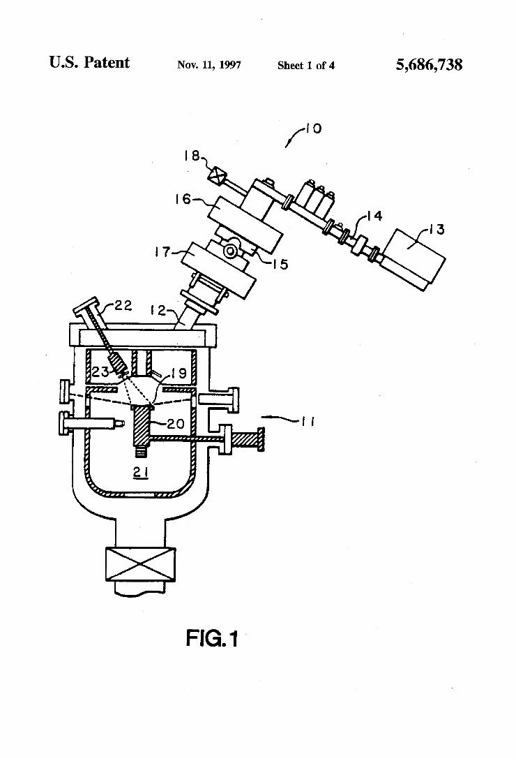
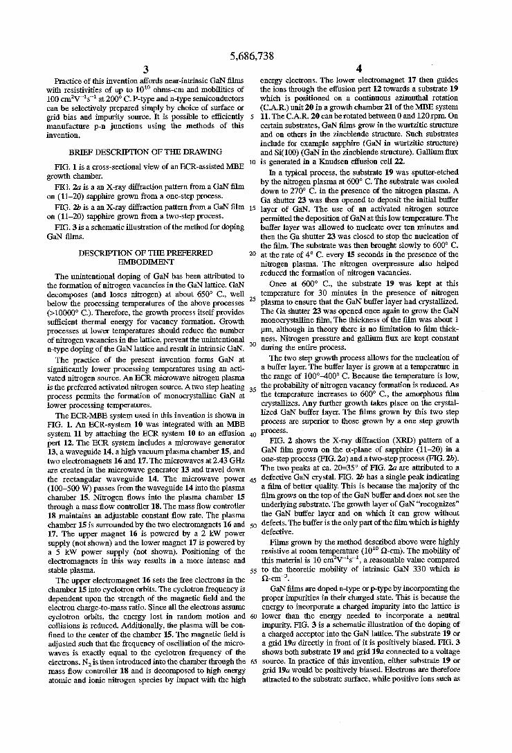
FIG. 1 is a cross-sectional view of an ECR-assisted MBE growth chamber. FIG.2a is a an X-ray diffraction pattern from a GaN film
on (11-20) sapphire grown from a one-step process. FIG.2b is a an X-ray diffraction pattern from a GaN film
on (11-20) sapphire grown from a two-step process. FIG. 3 is a schematic illustration of the method for doping
GaN films.
DESCRIPTION OF THE PREFERRED EMBODIMENT
The unintentional doping of GaN has been attributed to the formation of nitrogen vacancies in the GaN lattice. GaN decomposes (and loses nitrogen) at about 650° C., well below the processing temperatures of the above processes (>10000° C.). Therefore, the growth process itself provides sufficient thermal energy for vacancy formation. Growth processes at lower temperatures should reduce the number of nitrogen vacancies in the lattice, prevent the unintentional n-type doping of the GaN lattice and result in intrinsic GaN. The practice of the present invention forms GaN at
significantly lower processing temperatures using an acti wated nitrogen source. An ECR microwave nitrogen plasma is the preferred activated nitrogen source. Atwo step heating process permits the formation of monocrystalline GaN at lower processing temperatures. The ECR-MBE system used in this invention is shown in
FIG. 1. An ECR-system 10 was integrated with an MBE system 11 by attaching the ECR system 10 to an effusion pert 12. The ECR system includes a microwave generator 13, a waveguide 14, a high vacuum plasma chamber 15, and two electromagnets 16 and 17. The microwaves at 2.43 GHz are created in the microwave generator 13 and travel down the rectangular waveguide 14. The microwave power (100-500W) passes from the waveguide 14 into the plasma chamber 15. Nitrogen flows into the plasma chamber 15 through a mass flow controller 18. The mass flow controller 18 maintains an adjustable constant flow rate. The plasma chamber 15 is surrounded by the two electromagnets 16 and 17. The upper magnet 16 is powered by a 2 kW power supply (not shown) and the lower magnet 17 is powered by a 5 kW power supply (not shown). Positioning of the electromagnets in this way results in a more intense and stable plasma. The upper electromagnet 16 sets the free electrons in the
chamber 15 into cyclotron orbits. The cyclotron frequency is dependent upon the strength of the magnetic field and the electron charge-to-mass ratio. Since all the electrons assume cyclotron orbits, the energy lost in random motion and collisions is reduced. Additionally, the plasma will be con fined to the center of the chamber 15. The magnetic field is adjusted such that the frequency of oscillation of the micro waves is exactly equal to the cyclotron frequency of the electrons. Nis then introduced into the chamber through the mass flow controller 18 and is decomposed to high energy atomic and ionic nitrogen species by impact with the high
10
15
20
25
30
35
40
45
50
55
65
4 energy electrons. The lower electromagnet 17 then guides the ions through the effusion pert 12 towards a substrate 19 which is positioned on a continuous azimuthal rotation (C.A.R.) unit 20 in a growth chamber 21 of the MBE system 11. The C.A.R. 20 can be rotated between 0 and 120 rpm. On certain substrates, GaN films grow in the wurtzitic structure and on others in the zincblende structure. Such substrates include for example sapphire (GaN in wurtzitic structure) and Si(100) (GaN in the zincblende structure). Gallium flux is generated in a Knudsen effusion cell 22.
In a typical process, the substrate 19 was sputter-etched by the nitrogen plasma at 600° C. The substrate was cooled down to 270° C. in the presence of the nitrogen plasma. A Ga shutter 23 was then opened to deposit the initial buffer layer of GaN. The use of an activated nitrogen source permitted the deposition of GaN at this low temperature. The buffer layer was allowed to nucleate over ten minutes and then the Ga shutter 23 was closed to stop the nucleation of the film. The substrate was then brought slowly to 600° C. at the rate of 4° C. every 15 seconds in the presence of the nitrogen plasma. The nitrogen overpressure also helped reduced the formation of nitrogen vacancies.
Once at 600° C., the substrate 19 was kept at this temperature for 30 minutes in the presence of nitrogen plasma to ensure that the GaN buffer layer had crystallized. The Ga shutter 23 was opened once again to grow the GaN monocrystalline film, The thickness of the film was about 1 um, although in theory there is no limitation to film thick ness. Nitrogen pressure and gallium flux are kept constant during the entire process. The two step growth process allows for the nucleation of
a buffer layer. The buffer layer is grown at a temperature in the range of 100°–400° C. Because the temperature is low, the probability of nitrogen vacancy formation is reduced. As the temperature increases to 600° C., the amorphous film crystallizes. Any further growth takes place on the crystal lized GaN buffer layer. The films grown by this two step process are superior to those grown by a one step growth process.
FIG. 2 shows the X-ray diffraction (XRD) pattern of a GaN film grown on the o-plane of sapphire (11-20) in a one-step process (FIG. 2a) and a two-step process (FIG.2b). The two peaks at ca. 20=35° of FIG. 2a are attributed to a defective GaN crystal. FIG.2b has a single peak indicating a film of better quality. This is because the majority of the film grows on the top of the GaN buffer and does not see the underlying substrate. The growth layer of GaN “recognizes” the GaN buffer layer and on which it can grow without defects. The buffer is the only part of the film which is highly defective.
Films grown by the method described above were highly resistive at room temperature (10'Q-cm). The mobility of this material is 10 cm V's', areasonable value compared to the theoretic mobility of intrinsic GaN 330 which is Q-cm. GaN films are doped n-type or p-type by incorporating the
proper impurities in their charged state. This is because the energy to incorporate a charged impurity into the lattice is lower than the energy needed to incorporate a neutral impurity. FIG. 3 is a schematic illustration of the doping of a charged acceptor into the GaN lattice. The substrate 19 or a grid 19a directly in front of it is positively biased. FIG.3 shows both substrate 19 and grid 19a connected to a voltage source. In practice of this invention, either substrate 19 or grid 19a would be positively biased. Electrons are therefore attracted to the substrate surface, while positive ions such as

5,686.738 5
N are repelled. The growth process is carried out as described above with addition of an acceptor source 24 so that Ga, nitrogen and acceptor are deposited on the electron rich surface of the substrate. As the acceptor atom approaches the surface, it takes on an electron and is incorporated into the lattice as a negative species, the energy of incorporation being lower than that of the neutral acceptor species. The same procedure is used to dope the GaN lattice with donor impurities, except that a negative bias is used on the substrate or the grid. Alternately, a charged surface can be generated by bombarding the substrate with electrons or positive ions. Electron guns and ion guns, respectively, are conventional sources of these species.
Suitable acceptor species include, but are not limited to, zinc, magnesium, beryllium, and calcium. Suitable donor species include, but are not limited to, silicon, germanium, oxygen, selenium and Sulfur. What is claimed is: 1. A semiconductor device comprising: a substrate, said substrate consisting of a material selected from the group consisting of(100) Silicon, (111) silicon, (0.001) sapphire, (11-20) sapphire, (1-102) sapphire, (111) gallium are senide, (100) gallium aresenide, magnesium oxide, zinc oxide and silicon carbide;
a non-single crystalline buffer layer having a thickness of about 30 A to about 500A, comprising a first material grown on said substrate, the first material consisting essentially of gallium nitride; and
a first growth layer grown on the buffer layer, the first growth layer comprising gallium nitride and a first dopant material.
2. The semiconductor device of claim 1 further compris 1ng:
a second growth layer grown on the first growth layer, the second growth layer comprising gallium nitride and a second dopant material.
3. The semiconductor device of claim wherein the buffer layer is grown at a first temperature and wherein the first growth layer is grown at a second temperature higher than the first temperature.
4. The semiconductor device of claim 3 wherein the first temperature is in the range of about 100° C. to about 400° C.
5. The semiconductor device of claim 3 wherein the second temperature is in the range of about 600° C. to about 900° C.
6. The semiconductor device of claim 1 wherein the buffer layer is grown by exposing the substrate to gallium and nitrogen at the first temperature for about 3 to about 15 minutes.
7. The semiconductor device of claim 1 wherein the first dopant material is a donor.
8. A semiconductor device comprising: a substrate, said substrate consisting of a material selected from the group consisting of(100) silicon, (111) silicon, (0.001) sapphire, (11-20) sapphire, (1-102) sapphire, (111) gallium aresenide. (100) gallium aresenide, mag nesium oxide, zinc oxide and silicon carbide;
a non-single crystalline buffer layer, comprising a first material grown on said substrate, the first material consisting essentially of gallium nitride;
a first growth layer grown on the buffer layer, the first growth layer comprising gallium nitride and an accep tor dopant material;
a second growth layer grown on the first growth layer, the second growth layer comprising gallium nitride and a donor dopant material.
5
10
15
20
25
30
35
40
45
55
65
6 9. A semiconductor device comprising: a substrate, said substrate consisting of a material selected from the group consisting of (100) silicon, (111) silicon, (0001) sapphire, (11-20) sapphire, (1-102) sapphire, (111) gallium aresenide, (100) gallium aresenide, magnesium oxide, zinc oxide and silicon carbide;
a non-single crystalline buffer layer, comprising a fast material grown on said substrate, the first material consisting essentially of gallium nitride;
a first growth layer grown on the buffer layer, the first growth layer comprising gallium nitride and a first dopant material;
a second growth layer grown on the first growth layer, the second growth layer comprising gallium nitride and a second dopant material; and
wherein the first growth layer comprises a first conduc tivity type and the second growth layer comprises the opposite conductivity type.
10. The semiconductor device of claim 9 wherein the first conductivity type is n-type.
11. A semiconductor device comprising: a substrate, said substrate consisting of a material selected from the group consisting of 100) silicon, (111) silicon, (0.001) sapphire, (11-20) sapphire, (1-102) sapphire, (111) gallium aresenide, (100) gallium aresenide, mag nesium oxide, zinc oxide and silicon carbide;
a non-single crystalline buffer layer, comprising a first material grown on said substrate, the first material consisting essentially of gallium nitride;
a first growth layer grown on the buffer layer, the first growth layer comprising gallium nitride and a first dopant material;
wherein the buffer layer is a recrystallized, partially amorphous layer.
12. The semiconductor device of claim 3 wherein the buffer layer is a recrystallized, partially amorphous layer.
13. A semiconductor device comprising: a substrate, said substrate consisting of a material selected from the group consisting of (100) silicon, (111) silicon, (0001) sapphire, (11-20) sapphire, (1-102) sapphire, (111) gallium aresenide, (100) gallium aresenide, magnesium oxide, zinc oxide and silicon carbide;
a non-single crystalline buffer layer, comprising a first material grown on said substrate, the first material comprising gallium nitride; and
a near intrinsic gallium nitride layer grown on the buffer layer and having a resistivity of greater than 10 Q-cm. at room temperature.
14. The semiconductor device of claim 13, wherein the near intrinsic gallium nitride layer has a resistivity in the range of about 10 Q-cm to about 10' Q-cm at room temperature.
15. A semiconductor device having an activated p-type layer comprising:
a substrate, said substrate consisting of a material selected from the group consisting of (100) silicon, (111) silicon, (0.001) sapphire, (11-20) sapphire, (1-102) sapphire, (111) gallium are senide, (100) gallium aresenide, magnesium oxide, zinc oxide and silicon carbide;
a non-single crystalline buffer layer having a thickness of about 30 A to about 500 A comprising a first material grown on said substrate, the first material consisting essentially of gallium nitride; and

5,686,738 7
an activated p-type growth layer comprising gallium nitride and an acceptor dopant material formed without the use of a post-growth activation step.
16. A semiconductor device comprising: a substrate, said substrate consisting of a material selected from the group consisting of (100) silicon, (0.001) silicon, (0001) sapphire, (11-20) sapphire, (1-102) sapphire, (111) gallium aresenide, (100) gallium aresenide, magnesium oxide, zinc oxide and silicon carbide;
a non-single crystalline buffer layer having a thickness of about 30 A to about 500A grown on the substrate and comprising a first material consisting essentially of a Group III nitride grown at a temperature of about 100° C. to about 400° C. from a molecular Group III source and an activated nitrogen source in a molecular beam epitaxial growth chamber; and
a first growth layer grown on the buffer layer and com prising gallium nitride and a first dopant material, the first growth layer being grown at a temperature of at least about 600° C. from a molecular gallium source and an activated nitrogen Source in a molecular beam epitaxial growth chamber.
17. The semiconductor device of claim 16 wherein the Group III nitride is gallium nitride.
18. A semiconductor device comprising: a substrate, said substrate consisting of amaterial selected from the group consisting of (100) silicon, (111) silicon, (0001) sapphire, (11-20) sapphire, (1-102) sapphire, (111) gallium are senide, (100) gallium aresenide, magnesium oxide, Zinc oxide and silicon carbide;
a non-single crystalline buffer layer having a first thickness, comprising a first material grown on said substrate, the first material consisting essentially of gallium nitride; and
a growth layer grown on the buffer layer having a second thickness which is at least ten times greater than the first thickness, the growth layer comprising gallium nitride and a first dopant material.
19. A semiconductor device comprising: a substrate, said substrate consisting of a material Selected from the group consisting of (100) silicon, (111)
O
15
20
25
30
35
40
8 silicon, (0001) sapphire, (11-20) sapphire, (1-102) sapphire, (111) gallium aresenide, (100) gallium aresenide, magnesium oxide, Zinc oxide and silicon carbide;
a non-single crystalline buffer layer, comprising a first material grown on said substrate, the first material consisting essentially of gallium nitride; and
a growth layer grown on the buffer layer, the growth layer comprising gallium nitride and a first dopant material.
20. A semiconductor device having an activated p-type layer comprising:
a substrate, said substrate consisting of a material selected from the group consisting of 100) silicon, (111) silicon, (0.001) sapphire, (11-20) sapphire, (1-102) sapphire, (111) gallium aresenide, (100) gallium aresenide, mag nesium oxide, zinc oxide and silicon carbide;
a non-single crystalline buffer layer, comprising a mate rial grown on said substrate, the material consisting essentially of gallium nitride; and
an activated p-type growth layer comprising gallium nitride and a dopant material formed without the use of a post-growth activation step.
21. A semiconductor device comprising: a substrate, said substrate consisting of a material selected from the group consisting of (100) silicon, (111) silicon, (0.001) sapphire, (11-20) sapphire, (1-102) sapphire, (111) gallium aresenide, (100) gallium aresenide, magnesium oxide, zinc oxide and silicon carbide;
a non-single crystalline buffer layer grown on the sub strate and comprising a material consisting essentially of a Group III nitride grown at a temperature of about 100° C. to about 400° C. from a molecular Group III source and an activated nitrogen source in a molecular beam epitaxial growth chamber; and
a growth layer grown on the buffer layer and comprising gallium nitride and a first dopant material, the growth layer being grown at a temperature of at least about 600° C. from a molecular gallium source and an activated nitrogen source in a molecular beam epitaxial growth chamber.
: : :: i: :