UNIT V POWER SUPPLIES 5.1 RECTIFIERS YEAR/EC T34-EDC/Unit 5.pdf · UNIT – V POWER SUPPLIES 5.1...
24
UNIT – V POWER SUPPLIES 5.1 RECTIFIERS Diodes are referred to as non-linear circuit elements because of the above characteristic curve. For most applications the non-linear region can be avoided and the device can be modeled by piece-wise linear circuit elements. Qualitatively we can just think of an ideal diode has having two regions: a conduction region of zero resistance and an infinite resistance non-conduction region. For many circuit applications, this ideal diode model is an adequate representation of an actual diode and simply requires that the circuit analysis be separated into two parts: forward current and reverse current. Figure 5.1 shows a schematic symbol for a diode and the current-voltage curve for an ideal diode. Figure 5.1 a)Schematic symbol for a diode and b) current versus voltage for an ideal diode Figure 5.2 Equivalent circuit model of a junction diode
Transcript of UNIT V POWER SUPPLIES 5.1 RECTIFIERS YEAR/EC T34-EDC/Unit 5.pdf · UNIT – V POWER SUPPLIES 5.1...

UNIT – V
POWER SUPPLIES
5.1 RECTIFIERS
Diodes are referred to as non-linear circuit elements because of the above characteristic curve.
For most applications the non-linear region can be avoided and the device can be modeled by piece-wise
linear circuit elements. Qualitatively we can just think of an ideal diode has having two regions: a
conduction region of zero resistance and an infinite resistance non-conduction region. For many circuit
applications, this ideal diode model is an adequate representation of an actual diode and simply requires
that the circuit analysis be separated into two parts: forward current and reverse current. Figure 5.1 shows
a schematic symbol for a diode and the current-voltage curve for an ideal diode.
Figure 5.1 a)Schematic symbol for a diode and b) current versus voltage for an ideal diode
Figure 5.2
Equivalent circuit model of a junction diode

A diode can more accurately be described using the equivalent circuit model shown in figure 5.2. If a
diode is forward biased with a high voltage it acts like a resistor (Rf) in series with a voltage source (VPN).
For reverse biasing it acts simply as a resistor (Rr). These approximations are referred to as the linear
element model of a diode.
5.1.1 HALF-WAVE RECTIFIERS
Figure 5.3 shows a half-wave rectifier circuit. The voltage source VS is an AC source
……..(5.1)
of frequency radians per second, and Vm is the maximum or peak voltage. Note that
where f is the frequency in Hz. Generally, the source vS is the secondary winding of a transformer.
Figure 5.3 Half-wave rectifier
The diode is the component which does the rectification, since it permits current flow in one
direction only. The resistor RL represents the resistance of the load drawing the power.
Let's analyse this circuit assuming the diode is ideal. When vS > 0, the diode is forward biased,
and so switched on; therefore vout = vS. But when vS < 0, the diode is reverse biased, i.e. switched off, and
hence vout = 0 V. This is illustrated in Figure 5.4.
.

Figure 5.4 Half-wave rectifier waveforms
The load voltage waveform vout is always positive, and so has a non-zero DC component, the average
value VAVG which we calculate as follows:
……(5.2)
If we use the practical diode model to take into account the diode voltage drop, then we need to reduce Vm
by 0.7 V when forward biased:
Vm(out) = Vm - 0.7 V…….(5.3)
and the average voltage becomes
…..(5.4)
This means that the average voltage is reduced by the forward bias voltage drop across the diode.

The peak inverse voltage (PIV) is defined as the peak voltage across the diode when reverse biased: (note
that with zero current the voltage drop across RL is zero)
PIV = Vm……….(5.5)
The diode must be capable of withstanding this voltage.
5.1.2 FULL-WAVE RECTIFIERS
In the half-wave rectifier the voltage is zero for half of the cycle. Full-wave rectifiers are designed using
two or more diodes so that voltage is produced over the whole cycle.
Figure 5.5 shows a full-wave rectifier designed using two diodes and a center-tapped AC supply (i.e.
center-tapped transformer).
Figure 5.5 Center-tapped full-wave rectifier.
The waveforms are shown in Figure 5.6. The center tapping implies that the two source voltages v1 and v2
are a half cycle out of phase. We see that diode D1 conducts when source v1 is positive, and D2 conducts
when v2 is positive, giving the waveform vout.
.

Figure 5.6 Full-wave rectifier waveforms
The average or DC value of the waveform vout is now
……..(5.6)
since the waveform is non-zero twice as much as in the half-wave case. Here, Vm(out) equals Vm if we
regard the diodes as ideal, and equal to Vm -0.7 V if we use the practical model.
The peak inverse voltage is …..(5.7)
5.1.3 BRIDGE RECTIFIER
Figure shows a bridge rectifier built from four diodes and a single AC source. The waveform
of vout is the same as for the center-tapped full-wave rectifier.

Figure 5.7 Bridge full-wave rectifier
The average voltage for the bridge rectifier is the same as in HWR but the peak inverse voltage is
…….(5.8)
5.1.4 CAPACITOR FILTERS
It can be seen from Figures that the waveform vout is not very smooth. For many applications it is desired
to have a much smoother DC waveform, and so a filtering circuit is used. We will consider the filtered
half-wave rectifier of Figure, and leave the filtered full-wave rectifiers up to you to work out (not hard-see
lab).

Figure 5.7 Filtered Half-wave rectifier.
The waveform produced by this filtered half-wave rectifier is shown in figure 5.8 illustrating the ripple.
Figure 5.8 Ripple filtered Half-wave rectified
waveform.
Here, ripple is defined as the difference between the maximum and minimum voltages on the waveform,
Figure (i.e. peak-to-peak).

Figure 5.8 Filtered Half-wave rectified waveform showing Vrpp
and VDC.
The (peak-to-peak) ripple factor r is defined as
…..(5.9)
where Vrpp is the peak-to-peak ripple voltage and VDC is the DC component of the ripple waveform. T is
the period of the AC source voltage: T=1/f, . For f=50 Hz (the frequency of the AC supply in
Australia), T= 20 ms.
We now explain how to calculate (approximately) Vrpp and VDC. Think of the ripple waveform as being
approximated by a triangular waveform so that
…..(5.10)
Using symmetry. Suppose that at the beginning of a cycle the capacitor is fully charged to Vm(out), and that
the capacitor is large enough so that the time constant RL C is much larger than T. The rate of change of
vout at the beginning of the cycle t=0 is

…….(5.11)
so that at time t=T the capacitor voltage has decreased by an amount
…….(5.12)
approximately (straight line approximation). This allows one to design C for a given load and desired
ripple.
Exercise. Show that Vrpp in the case of a full-wave rectifier is given by
…….(5.13)
Figure 5.9 Approximate (triangular) filtered Half-wave rectified waveform

5.2 VOLTAGE REGULATORS:
The function of a voltage regulator is to provide a stable dc voltage for powering other electronic
circuits. A voltage regulator should be capable of providing substantial output current. Voltage
regulators are classified as:
Series regulator
Switching regulator
Series regulators use power transistor connected in series between the
unregulated dc input and the load. The output voltage is controlled by the continuous voltage
drop taking place across the series pass transistor. Since the transistor conducts in the active or
linear region, these regulators are also called linear regulators. Linear regulators may be fixed or
variable output voltage and could be positive or negative. The schematic, important
characteristics, data sheet, short circuit protection, current fold-back, current boosting techniques
for linear voltage regulators such as 78 XX series, 723 IC are discussed.
Switching regulators, on the hand, operate the power transistor as a high
frequency on/off switch, so that the power transistor does not conduct current continuously. This
gives improved efficiency over series regulator.
5.2.1 SERIES OP-AMP REGULATOR
A voltage regulator is an electronic circuit that provides a stable dc voltage
independent of the load current, temperature and ac line voltage variations.
The above circuit shows a regulated supply.
The circuit consists of the following four parts:
1. Reference voltage circuit
2. Error amplifier
3. Series pass transistor
4. Feedback network
The power transistor Q1 is in series with unregulated dc voltage Vin and regulated
output voltage Vo.
Whenever any fluctuation in the output voltage occurs, it must absorb the difference
between the two voltages.
The transistor Q1 is also connected as an emitter follower and therefore provides the
sufficient current gain to drive the load.
The output voltage is sampled by the R1-R2 divider and feedback to the negative input
terminal of the op-amp error amplifier.
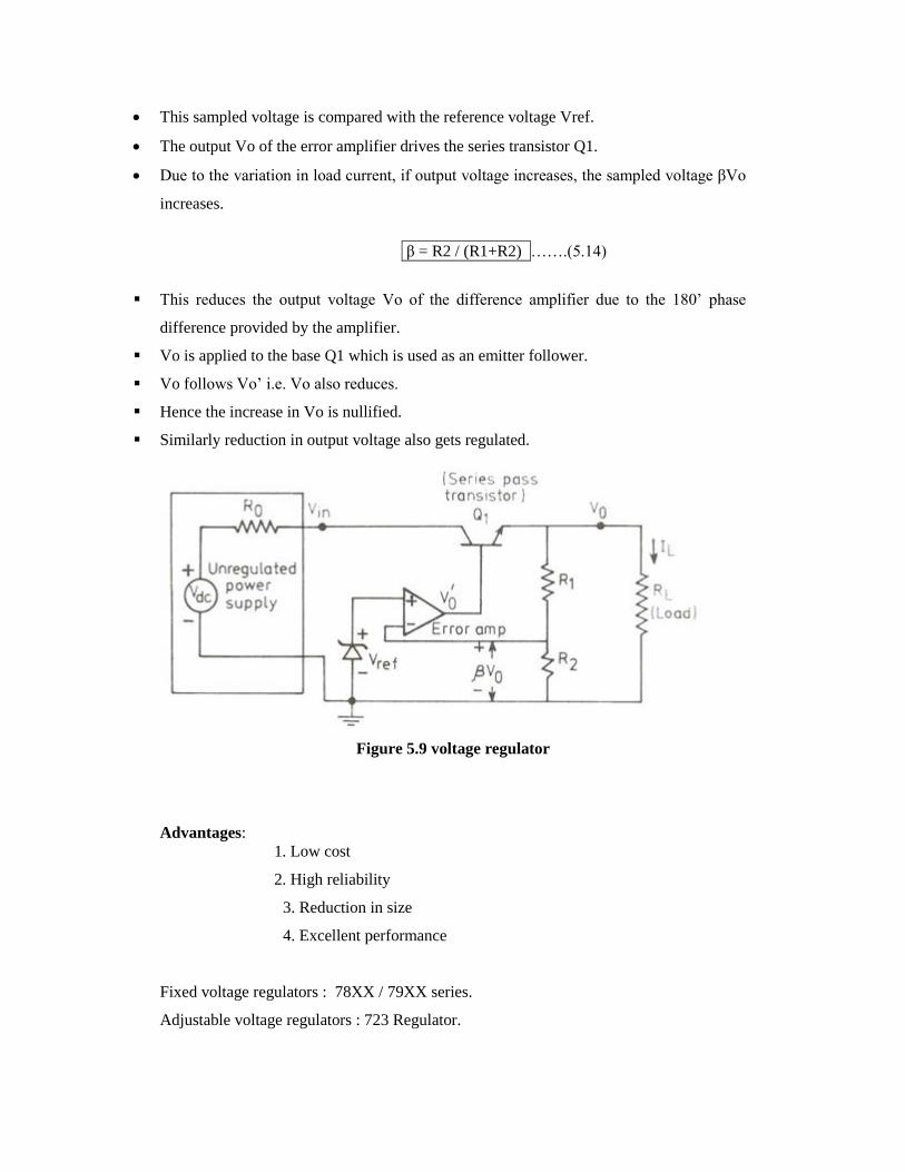
This sampled voltage is compared with the reference voltage Vref.
The output Vo of the error amplifier drives the series transistor Q1.
Due to the variation in load current, if output voltage increases, the sampled voltage βVo
increases.
β = R2 / (R1+R2) …….(5.14)
This reduces the output voltage Vo of the difference amplifier due to the 180‟ phase
difference provided by the amplifier.
Vo is applied to the base Q1 which is used as an emitter follower.
Vo follows Vo‟ i.e. Vo also reduces.
Hence the increase in Vo is nullified.
Similarly reduction in output voltage also gets regulated.
Figure 5.9 voltage regulator
Advantages:
1. Low cost
2. High reliability
3. Reduction in size
4. Excellent performance
Fixed voltage regulators : 78XX / 79XX series.
Adjustable voltage regulators : 723 Regulator.

5.2.2 IC REGULATOR
5.2.2.1 FIXED VOLTAGE REGULATOR
(1) POSITIVE FIXED VOLTAGE REGULATORS.
78XX series are three terminal, positive fixed regulators.In 78XX, the last two
numbers „XX‟ indicate the output voltage.There are seven output voltage options
available such as 5, 6, 8,12,15,18 and 24V.For example 7805 represents 5V regulator.
Figure 5.9 Positive fixed regulators
The above figure 5.9 shows the standard representation of monolithic 5 voltage regulator. A
capacitor Cin (0.33 μF ) is usually connected between the input terminal and ground to cancel
the inductive effect due to long distribution leads. The output capacitor Co (1 μF ) improves
the transmit response.
Characteristics:
The regulated output voltage is fixed at a value specified by the manufacturer. For e.g.
78XX series has a output voltage at 5, 6, 8 etc.,
The unregulated input voltage must be at least 2V more than the regulated output voltage
i.e. | Vin | >= Vo +2 volts. For example, if 7805 regulator has Vo = 5V then Vin = 7V
The load current Iomax may vary from 0 to rated maximum output current.
Thermal shunt down : the IC has a temperature sensor (built-in) which turns off IC when
it becomes too hot. The output current will drop and remain there until the IC has cooled
significantly.
(2)Negative fixed voltage regulator:
79XX series of fixed output are negative voltage regulators.
They are complement to the 78XX series.

In addition to voltage options available in 78XX series, there are two extra
voltage options of -2V and -5.2V available in 79XX series.
The constructional detail is as same that of 78XX series.
For example 7905 represents 5V regulator.
Figure 5.10 Negative fixed voltage regulator
5.2.3 VARIABLE VOLTAGE REGULATOR
The three terminal regulators discussed earlier have the following limitations
1.No short circuit operation
2. Output voltage is fixed.
These limitations have been overcome in the 723 general purpose regulator, which can be
adjusted over a wide range of both positive or negative regulated voltage. This IC is
inherently low current device, but can be boosted to provide 5 amps or more current by
connecting external components.
Limitation:
It also has no short circuit current limits.
It has no in-built thermal protection.

Figure 5.11 723 general purpose regulator
Figure 5.12 Low voltage regulator
5.2.4 BOOSTING OUTPUT CURRENT FOR FIXED IC REGULATOR:
It is possible to boost the output current of a three terminal regulator by connecting an
external pass transistor in parallel with the regulator.
For low load currents, the voltage drop across R1 is insufficient (<0.7 V) to turn on
transistor Q1 and the regulator itself is able to supply the load current.

As IL increases, the voltage drop across R1 increases.
When the voltages drop is ~ 0.7 V, the transistor Q1 turns on.
For example if IL = 100 mA;
Voltage drop across R1 = 7 Ώ * 100 mA
= 0.7 mA.
Thus if IL increases more than 100 mA, the transistor Q1 turns on and supplies the
constant extra current required.
Since Veb (ON) remains fairly constant, the excess current comes from Q1 and base after
amplification by β.
The regulator adjusts IB so that IL=IC+I0
IC=βIB
For the regulator
Io=Ii-Iq
QiO III
iI ( as IQ is small )
1RiB III
1
)(
R
VI
onEBO
The maximum current Io(max) for a 7805 regulator is 1A from the data, assuming
Veb(on)= 1 V& = 15 we get from equation (8),
Figure 5.13 Fixed voltage regulator

5.2.4 VARIABLE VOLTAGE REGULATOR
The three terminal regulators discussed earlier have the following limitations
1.No short circuit operation
2. Output voltage is fixed.
These limitations have been overcome in the 723 general purpose regulator, which can be
adjusted over a wide range of both positive or negative regulated voltage. This IC is
inherently low current device, but can be boosted to provide 5 amps or more current by
connecting external components.
LIMITATION:
It also has no short circuit current limits.
It has no in-built thermal protection.
Figure 5.12 723 IC Low voltage regulator

Figure 5.12 Functional block for a Low voltage regulator
5.3 CURRENT FOLD BACK:
Current foldback is the method which will limit the short circuit current and yet allow
higher current to the load.
The curve given below shows the current foldback characteristics curve.
As current demand increases the output voltage is held constant till a preset current level
(I knee) is reached.
If the current demand exceeds this level, both output voltage and output current
decreases.
The figure given below shows the method of applying current foldback.

The circuit given below tells about the operation of the current fold back.
Figure 5.13 a. current fold back characteristic curve b. current fold back
The voltage at terminal CL is divided by R3-R4 network.
The current limit transistor Q2 conducts only when the drop across the resistance Rsc is
large enough to produce base emitter voltage of Q2 to be atleast 0.5 V.
As Q2 starts conduction, transistor Q1 begins to turn off and the current IL decreases .
This reduces the voltage v1 at the emitted of Q1 and also the output voltage vo .
Voltage at the base of Q1= v1R4/(R3+R4)
Thus the voltage at the CL terminal drops by a smaller amount compared to the drop in
voltage at Cs terminal.

This increases Vbe of Q2 thereby increasing the conduction of Q2 which in turn reduces
the conduction of Q1 i.e., the current IL further reduces.
This process continue till Vo=0 V & V1 is just large enough to keep 0.5 v between CL &
Cs terminal.
This point is Isc & has been reduced by lowering both IL & Vo.
5.4 CURRENT BOOSTING FOR VARIABLE REGULATOR:
The maximum current that 723 IC regulator can provide is 140 mA.
It is possible to boost the current level by adding a boost transistor Q1 to the voltage
regulator .
The circuit given below is current boosted low voltage regulator.
The collector current of the pass transistor Q1 comes from the unregulated d.c power
supply.
The output current from Vo terminal drives the base of the pass transistor Q1.
This base current gets multiplied by the beta of the pass transistor, so that 723 has to
provide only the base current.
Iload = pass transistor x Io(723)
Figure 5.13 Current Boosting For Variable Regulator
5.5 PRODUCTION OF SWITCHING:
They can be done in the following ways:
1.Current limit protection (or) short circuit protection
2.Over voltage protection

5.5.1 CURRENT LIMIT PROTECTION (OR) SHORT CIRCUIT PROTECTION:
If the load demands more current i.e. under short circuit conditions, the IC tries to
provide it at a constant output voltage getting hotter all the time. This may ultimately
burn the IC.
In order to prevent the IC, it is provided with the current limit facility.
Current limiting refers to the ability of the regulator to prevent the load current from
increasing above a preset value.
The characteristic curve of a current limited power supply is shown below in figure a.
The output voltage remains constant for load current below Ilimit.
As current approaches the limit, the output voltage drops.
The current limit Ilimit is set by connecting an external resistor Rsc between the terminals
CL & CS terminals as shown below:
Figure 5.13 a. Current Limit Protection characteristic curve b. Current Limit
Protection

5.5.2 CURRENT LIMIT PROTECTION
The CL terminal is also connected to the output terminal Vo.
The CS terminal is connected to the load.
The load current produces a small voltage drop Vsense across RSC.
The voltage Vsense is applied directly across the base emitter junction of Q2.
When this voltage is approximately equal to 0.5 V, transistor Q2 begins to turn ON.
A part of the current from the error amplifier goes to the collector of Q2, thereby
decreasing the base current of Q1.
This in turn, reduces the emitter current of Q1.
Therefore any increase in the load current will get nullified.
Similarly if the load current decreases, VBE of Q2 drops.
This cycle is repeated in such a way that the load current is held constant to produce a
voltage across RSC sufficient to turn Q2 ON.
This voltage is typically 0.5 V.
Ilimit = Vsense / RSC = 0.5 V/RSC.
5.5.3 OVER VOLTAGE PROTECTION:
The over voltage problems are divided into two types:
Spikes
Surges
Spikes are high voltage transients, which last for short duration of few μs.
Surges are high voltage transients, which will last for longer duration and will stretch for
many microsecond or millisecond.
Spike and surge protectors are designed to prevent over voltages from reaching the
system. They absorb the excess voltages before they enter the system.
Surge protectors are connected between the system and the power line.
The most common over voltage protection devices are the metal oxide varistors.
They can chop and shunt away all voltages above a certain level.
These devices are designed to accept voltages as high as 6000 V and divert any voltage above
200 V to ground. Excess energy does not disappear but turns into heat possibly destroying the
varistors.The most important characteristics of these devices are, “how fast they work and
how much energy they can dissipate”.
Example of surge protectors:

Semiconductors
Ionized spark gaps
Ferro resonant transformers.
5.5.4 SWITCHING REGULATOR:
It is also called switched mode regulator.
In the case of series regulator, the pass transistor is operated in it‟s linear region to
provide a controlled voltage drop across it with a steady dc current flow.
In the case of switched mode regulator, the pass transistor is used as “controlled switch”
and is operated at either cutoff or saturated state.
In the case of series regulator, the efficiency is very low.
In the case of switched mode regulator, the efficiency is high i.e in the range of 70-90%.
In the following diagram, we shall discuss the operation of switched mode power supply
(SMPS).

Figure 5.14 SPS

Figure 5.15 SPS Waveforms