UNIT 4 Instruction Sets
122
UNIT 4 Instruction Sets
Transcript of UNIT 4 Instruction Sets

UNIT 4Instruction Sets

What is Microprocessor
• A microprocessor, sometimes called a logic chip,is a computer processor on a microchip.
• It is also called as “Heart of Computer.”
• The microprocessor contains all, or most of, thecentral processing unit (CPU) functions.
• A microprocessor is designed to performarithmetic and logic operations that make use ofsmall number-holding areas called Registers.
2Prof. R. V. Bidwe, PICT, Pune.

• Typical microprocessor operations includeadding, subtracting, comparing two numbers,and fetching numbers from one area toanother.
• These operations are the result of a set ofinstructions that are part of themicroprocessor design.
3Prof. R. V. Bidwe, PICT, Pune.

Three basic characteristics differentiate Microprocessors:
• Instruction set: The set of instructions that themicroprocessor can execute.
• Bandwidth : The number of bits processed in asingle instruction.
• Clock speed : Given in megahertz (MHz), theclock speed determines how many instructionsper second the processor can execute.
In both cases, the higher the value, the morepowerful the CPU.
For example, a 32-bit microprocessor that runs at50MHz is more powerful than a 16-bitmicroprocessor that runs at 25MHz.
4Prof. R. V. Bidwe, PICT, Pune.

Microprocessor Vs. Microcontroller
Prof. R. V. Bidwe, PICT, Pune. 5
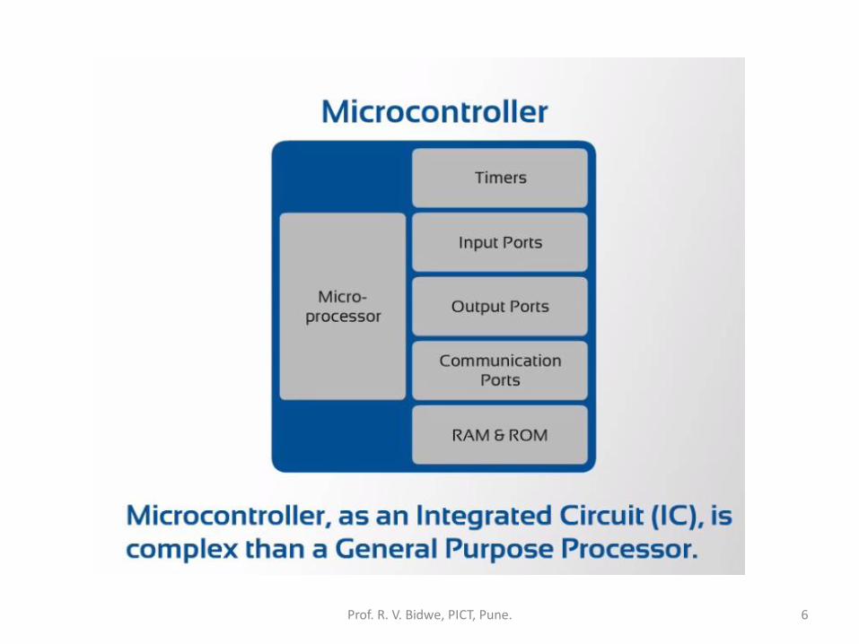
Prof. R. V. Bidwe, PICT, Pune. 6

Prof. R. V. Bidwe, PICT, Pune. 7

How It Looks: 8086 Processor Kit
Prof. R. V. Bidwe, PICT, Pune. 8

Pinless Microprocessor
Prof. R. V. Bidwe, PICT, Pune. 9

Prof. R. V. Bidwe, PICT, Pune. 10

History of MicroprocessorMP Introduction Data Bus (In Bits) Address Bus (In Bits)
4004 1971 4 8
8008 1972 8 8
8080 1974 8 16
8085 1977 8 16
8086 1978 16 20
80186 1982 16 20
80286 1983 16 24
80386 1986 32 32
80486 1989 32 32
Pentium 1993 onwards 32
Core solo 2006 32
Dual Core 2006 32
Core 2 Duo 2006 32
Core to Quad 2008 32
I3,i5,i7 2010 64 40Prof. R. V. Bidwe, PICT, Pune. 11

Microprocessor Functions
• Microprocessor functions mainly involve
– Instruction Fetch and Execute
– Interrupts
– I/O Function
Prof. R. V. Bidwe, PICT, Pune. 12

About 8086
• It is 16 bit processor. So that it has 16 bit ALU,16 bit registers and internal data bus and 16bit external data bus.
• 8086 has 20 bit address lines to accessmemory. Hence it can access.
2^20 = 1 MB memory location
13Prof. R. V. Bidwe, PICT, Pune.

• Pipelining:-8086 uses two stage of pipelining.First is Fetch Stage and the second is ExecuteStage.
– Fetch stage that prefetch upto 6 bytes ofinstructions stores them in the queue.
– Execute stage that executes these instructions.
• Pipelining improves the performance of theprocessor so that operation is faster.
• Segmentation divides memory into 4 parts.
14Prof. R. V. Bidwe, PICT, Pune.

• Operates in two modes:-8086 operates in twomodes:– Minimum Mode: A system with only one
microprocessor.– Maximum Mode: A system with multiprocessor.
• 8086 uses memory banks:-The 8086 uses amemory banking system. It means entire data isnot stored sequentially in a single memory of 1MB but memory is divided into two banks of512KB.
• Interrupts:-8086 has 256 vectored interrupts.
15Prof. R. V. Bidwe, PICT, Pune.

• Multiplication And Division:-8086 has apowerful instruction set. So that it supportsMultiply and Divide operation.
16Prof. R. V. Bidwe, PICT, Pune.
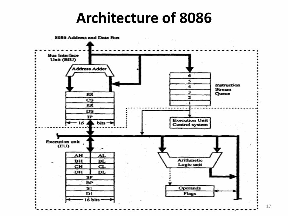
Architecture of 8086
17Prof. R. V. Bidwe, PICT, Pune.

Architecture of 8086
• The architecture of 8086 includes
– Arithmetic Logic Unit (ALU)
– Flag Register
– General Registers
– Instruction Stream Byte Queue
– Segment Registers
18Prof. R. V. Bidwe, PICT, Pune.

EU & BIU• The 8086 CPU logic has been partitioned into two
functional units namely Bus Interface Unit (BIU)and Execution Unit (EU).
• The major reason for this separation is toincrease the processing speed of the processor.
• The BIU has to interact with memory and inputand output devices in fetching the instructionsand data required by the EU.
• EU is responsible for executing the instructions ofthe programs and to carry out the requiredprocessing.
19Prof. R. V. Bidwe, PICT, Pune.

BUS INTERFACE UNIT (BU)
The BIU performs all bus operations for EU.
– Fetching instructions
– Responsible for executing all external bus cycles.
– Read operands and write result.
EXECUTION UNIT (EU)
Execution unit contains the completeinfrastructure required to execute aninstruction.
20Prof. R. V. Bidwe, PICT, Pune.

Bus Interface Unit
• The BIU has
– Instruction Byte Queue
– Segment Registers
– Instruction Pointer
21Prof. R. V. Bidwe, PICT, Pune.

BIU – Instruction Byte Queue
• 8086 instructions vary from 1 to 6 bytes.
• Therefore fetch and execution are takingplace concurrently in order to improve theperformance of the microprocessor.
• The BIU feeds the instruction stream to theexecution unit through a 6 byte prefetchqueue.
22Prof. R. V. Bidwe, PICT, Pune.

BIU – Instruction Byte Queue
• Execution and decoding of certain instructions donot require the use of buses.
• While such instructions are executed, the BIUfetches up to six instruction bytes for thefollowing instructions (subsequent instructions).
• The BIU store these prefetched bytes in a first-in-first out register by name instruction byte queue.
• When the EU is ready for its next instruction, itsimply reads the instruction byte(s) for theinstruction from the queue in BIU.
23Prof. R. V. Bidwe, PICT, Pune.

• Segment Registers
24Prof. R. V. Bidwe, PICT, Pune.

Different Areas in Memory
• Program memory – The executable programs from thememory.
• Data memory – The processor can access the secondarydata in any one out of four available segments.
• Stack memory – A stack is a section of the memory setaside to store addresses and data while a subprogramexecutes.
• Extra segment – This segment is also similar to datamemory where additional secondary data may be storedand maintained.
25Prof. R. V. Bidwe, PICT, Pune.

Segment Registers
• Code Segment (CS) register is a 16-bit registercontaining address of 64 KB segment with ProcessorInstructions.
• The processor uses CS segment for all accesses toinstructions referenced by Instruction Pointer (IP)register.
• Stack Segment (SS) register is a 16-bit registercontaining address of 64KB segment with ProgramStack.
• By default, the processor assumes that all datareferenced by the Stack Pointer (SP) and Base Pointer(BP) registers is located in the stack segment.
26Prof. R. V. Bidwe, PICT, Pune.

• Data Segment (DS) register is a 16-bit registercontaining address of 64KB segment with ProgramData.
• By default, the processor assumes that all datareferenced by general registers (AX, BX, CX, DX) andIndex Register (SI, DI) is located in the data segment.
• Extra Segment (ES) register is a 16-bit registercontaining address of 64KB segment, usually withProgram Data.
• By default, the processor assumes that the DIregister references the ES segment in stringmanipulation instructions.
27Prof. R. V. Bidwe, PICT, Pune.

Execution Unit
• The Execution Unit (EU) has
– Control Unit
– Arithmetic And Logical Unit (ALU)
– General Registers
– Flag Register
– Pointers
– Index Registers
28Prof. R. V. Bidwe, PICT, Pune.

Execution Unit
• Control unit is responsible for the co-ordination of all other units of the processor.
• ALU performs various arithmetic and logicaloperations over the data.
• The Control Unit translates the instructionsfetched from the memory into a series ofactions that are carried out by the EU.
29Prof. R. V. Bidwe, PICT, Pune.

Programmer’s Model of 8086
• General Purpose Register
30Prof. R. V. Bidwe, PICT, Pune.

31Prof. R. V. Bidwe, PICT, Pune.

• Flag Register
32Prof. R. V. Bidwe, PICT, Pune.

Pin Diagram 8086
33Prof. R. V. Bidwe, PICT, Pune.

Prof. R. V. Bidwe, PICT, Pune. 34

8086 can be work in two modes
• Minimum Mode: For single processor systems.
• Maximum Mode: For system with two or more processors.
Depending upon modes signals can be divided into
• Signals having common functions in both modes
• Signals for Minimum Mode
• Signals for Maximum Mode
35Prof. R. V. Bidwe, PICT, Pune.

Signals having common functions in both modes
• AD15 – AD0: Address /Data Bus (BI)T1 state: Address Bus
T2,T3,Tw and T4: Data Bus
• A19/S6 - A16/S3: Address/Status (OP)
T1 state : used to address upper 4 bits of address.
T2, T3, Tw and T4 : Used to output status.
S3 and S4 indicates segment registers being used
S5: Status of Interrupt enable flag updated every clock cycle.
S6: When 8086 Shared system bus, then goes low or goes high.36Prof. R. V. Bidwe, PICT, Pune.

• BHE(#)/S7: BHE (Bus High Enable) (OP)
Low: If transfer is using higher order bytes (AD15-AD8)
High: If transfer is using lower order bytes (AD7-AD0)
S7 is used with HOLD Pin. BHE A0 Characteristics
0 0 Whole word
0 1 Upper byte from/to odd address
1 0 Lower byte from/to even address
1 1 None37Prof. R. V. Bidwe, PICT, Pune.

• NMI (NON-MASKABLE INTERRUPT) (IP)Interrupts can not be avoided.
• RESET: (IP)Causes the processor to immediately terminate its present
activity.
• CLK: (IP)Provides the basic timing for the processor and bus controller.
Power supply given to the system is converted to CLK signals by theClock Generator.
• READY: (IP)It is the acknowledgement from the addressed memory or I/O
device that it is ready for the data transfer. Otherwise 8086 will moveto wait state.
38Prof. R. V. Bidwe, PICT, Pune.

• TEST (#): (IP)This signal is used by WAIT instruction. Execution will continue, until
TEST is low else it will be in idle state. TEST is synchronized internally duringeach clock cycle.
• RD (#): (OP)This signal remains low when 8086 is reading data from memory or I/O
devices.
• MN/MX (#): (IP)Indicates what mode the processor is to operate in.
• GND: Ground (OP)To prevent 8086 from thermal heating ,two ground signals are used.
• VCC: (IP)+5V power supply pin.
39Prof. R. V. Bidwe, PICT, Pune.

Signals functions in Maximum modes
• QS1,QS0 : (OP)
Reflects status of Instruction Queue.
• S2,S1,S0 (#): (OP)Indicates type of transfer takes place during current bus cycle.
QS1 QS0 Status
0 0 No Operation
0 1 First Byte of Op Code from Queue
1 0 Queue is empty
1 1 Subsequent Byte from Queue
S2 S1 S0 Machine Cycle
0 0 0 Interrupt ACK
0 0 1 I/O Read
0 1 0 I/O Write
0 1 1 Halt
S2 S1 S0 Machine Cycle
1 0 0 Instruction Fetch
1 0 1 Memory Read
1 1 0 Memory Write
1 1 1 Inactive-Passive (In T3)40Prof. R. V. Bidwe, PICT, Pune.

• LOCK: (OP)Bus is not used by another processor, current system
have locked the rights. Used for notifying to another processors.
• RQ(#)/GT1(#)&RQ(#)/GT0(#):
(Bus request/Bus Grant) (BI)
Using bus request signal another master can request asystem bus and processor sends a grant signal as a acceptance.
RQ/GT0 is having greater priority than RQ/GT1.
41Prof. R. V. Bidwe, PICT, Pune.

Signals functions in Minimum modes
• INTA (Interrupt Ack): (OP)It indicates recognition of an interrupt request. It then sends
two negative going pulse in next to clk cycles, first informs interfacethat its interrupt request in accepted, in next pulse interface replieswith interrupt type.
• ALE (Address Latch Enable): (OP)It is provided to demultiplex AD0-AD15 to A0-A15 and D0-
D15.
• DEN (#) (Data Enable): (OP)This signal informs transceivers that 8086 is ready to send or
receive data.
42Prof. R. V. Bidwe, PICT, Pune.

• DT/R (#) (Data Transmit/Receive): (OP)It is used to control the direction of data flow through the
transceiver.
High: 8086 is transmitting data
Low: 8086 is receiving data
• M/IO (#) : (OP)It is used to distinguish a memory access from an I/O
access.
High: Memory Access
Low: I/O Access
• WR (#) (WRITE): (OP)Indicates that the processor is performing a writing data
to memory or I/O.
43Prof. R. V. Bidwe, PICT, Pune.

• HOLD (IP) / HLDA (OP) :HOLD: indicates that DMA master is requesting a local
bus, on request processor replies High HLDA signal as a Ack.
44Prof. R. V. Bidwe, PICT, Pune.

Minimum-Mode and Maximum-Mode System (cont.)
Signals common to both minimum and maximum mode 45Prof. R. V. Bidwe, PICT, Pune.

Minimum-Mode and Maximum-Mode System (cont.)
Unique minimum-mode signals
46Prof. R. V. Bidwe, PICT, Pune.

Minimum-Mode and Maximum-Mode System (cont.)
Unique maximum-mode signals
47Prof. R. V. Bidwe, PICT, Pune.

Segmentation in 8086
• The process of dividing memory is calledSegmentation.
• Intel 8086 has 20 lines address bus.
• With 20 address lines, the memory that can beaddressed is 2^20 bytes
2^20 = 1,048,576 bytes (1 MB).
• 8086 can access memory with address ranging from00000 H to FFFFF H.
48Prof. R. V. Bidwe, PICT, Pune.

49Prof. R. V. Bidwe, PICT, Pune.

• In 8086, memory has four different types ofsegments.
These are:
– Code Segment
– Data Segment
– Stack Segment
– Extra Segment
• These registers are 16-bit in size.
• Each register stores the base address (startingaddress) of the corresponding segment.
• Because the segment registers cannot store 20 bits,they only store the upper 16 bits.
50Prof. R. V. Bidwe, PICT, Pune.

Logical to physical address Translation in 8086
• The 20-bit address of a byte is called its PhysicalAddress.
• High level languages have a Logical Address.
• Logical address is in the form of:
Base Address : Offset
• Offset is the displacement of the memory locationfrom the starting location of the segment.
51Prof. R. V. Bidwe, PICT, Pune.

Example• The value of Data Segment Register (DS) is 2222 H.
• To convert this 16-bit address into 20-bit, the BIUappends 0H to the LSBs of the address.
• After appending, the starting address of the DataSegment becomes 22220H.
• If the data at any location has a logical addressspecified as:
2222 H : 0016 H
• Then, the number 0016 H is the offset. 2222 H is thevalue of DS.
52Prof. R. V. Bidwe, PICT, Pune.

• To calculate the effective address of the memory, BIUuses the following formula:
Effective Address =
Starting Address of Segment + Offset
• To find the starting address of the segment, BIUappends the contents of Segment Register with 0H.
• Then, it adds offset to it.
Therefore:
EA = 22220 H
+ 0016 H
------------
22236 H53Prof. R. V. Bidwe, PICT, Pune.

54Prof. R. V. Bidwe, PICT, Pune.

Question 1
The contents of the following registers are:
• CS = 1111 H
• DS = 3333 H
• SS = 2526 H
• IP = 1232 H
• SP = 1100 H
• DI = 0020 H
Calculate the corresponding physical addresses for the address bytes in CS, DS and SS.
55Prof. R. V. Bidwe, PICT, Pune.

1. CS = 1111 H• The base address of the code segment is 11110 H.• Effective address of memory is given by 11110H +
1232H = 12342H.
2. DS = 3333 H• The base address of the data segment is 33330 H.• Effective address of memory is given by 33330H +
0020H = 33350H.
3. SS = 2526 H• The base address of the stack segment is 25260 H.• Effective address of memory is given by 25260H +
1100H = 26360H.
56Prof. R. V. Bidwe, PICT, Pune.

Question 2
The contents of the following registers are:
• CS = 1234 H
• ES = 0014 H
• SS = 9526 H
• IP = 0042 H
• SP = 1800 H
• DI = 2020 H
Calculate the corresponding physical addresses for the address bytes in CS, ES and SS.
57Prof. R. V. Bidwe, PICT, Pune.

1. CS = 1234 H• The base address of the code segment is 12340 H.• Effective address of memory is given by 12340H +
0042H = 12382H.
2. ES = 0014 H• The base address of the data segment is 00140 H.• Effective address of memory is given by 00140H +
2020H = 02160H.
3. SS = 9526 H• The base address of the stack segment is 95260 H.• Effective address of memory is given by 95260H +
1800H = 96A60H.
58Prof. R. V. Bidwe, PICT, Pune.

Assemblers, Linkers & Loaders
59Prof. R. V. Bidwe, PICT, Pune.

60Prof. R. V. Bidwe, PICT, Pune.

61Prof. R. V. Bidwe, PICT, Pune.

62Prof. R. V. Bidwe, PICT, Pune.

63Prof. R. V. Bidwe, PICT, Pune.

64Prof. R. V. Bidwe, PICT, Pune.

65Prof. R. V. Bidwe, PICT, Pune.

66Prof. R. V. Bidwe, PICT, Pune.

Procedures
Prof. R. V. Bidwe, PICT, Pune. 67

Why Procedures?
Prof. R. V. Bidwe, PICT, Pune. 68

Nested Procedures
Prof. R. V. Bidwe, PICT, Pune. 69

Macros
Prof. R. V. Bidwe, PICT, Pune. 70

Macros as Inline codes
Prof. R. V. Bidwe, PICT, Pune. 71

Difference between Macro and Procedure
Prof. R. V. Bidwe, PICT, Pune. 72

How to define macro
section .data
msg: db “hello”,10len: equ $-msg
Section .bss
count: resb 2
%macro print 2Mov rax,1Mov rdi,1Mov rsi, %1Mov rdx, %2Syscall%endmacro
Section .textGlobal mainMain:-print msg,len--print msg,len---; code of addition and result stored in COUNT variableprint count,2--Mov rax,60Mov rdi,0syscall
Prof. R. V. Bidwe, PICT, Pune. 73

Stack
74Prof. R. V. Bidwe, PICT, Pune.

Directives
• There are some instructions in the assemblylanguage program which are not a part ofProcessor Instruction Set.
• These instructions are instructions to theAssembler, Linker and Loader. These arereferred to as pseudo-operations or asassembler directives.
75Prof. R. V. Bidwe, PICT, Pune.

• DB – Define Byte
• DD – Define Doubleword
• DQ – Define Quadword
• DT – Define Ten Bytes
• DW – Define Word
• ENDS
• This directive is used with name of the segment to indicate the end of that logic segment.
CODE SEGMENT ; this statement starts the segment
CODE ENDS ; this statement ends the segment
• EQU
76Prof. R. V. Bidwe, PICT, Pune.

77Prof. R. V. Bidwe, PICT, Pune.

78Prof. R. V. Bidwe, PICT, Pune.

Prof. R. V. Bidwe, PICT, Pune. 79

• Flag Manipulation instructions
The Flag manipulation instructions directly modify some of the Flags of 8086.i. CLC – Clear Carry Flag.ii. CMC – Complement Carry Flag.iii. STC – Set Carry Flag.iv. CLD – Clear Direction Flag.v. STD – Set Direction Flag.vi. CLI – Clear Interrupt Flag.vii. STI – Set Interrupt Flag.
• Machine Control instructions
The Machine control instructions control the bus usage and executioni. WAIT – Wait for Test input pin to go low.ii. HLT – Halt the process.iii. NOP – No operation.iv. ESC – Escape to external device like NDPv. LOCK – Bus lock instruction prefix.
Prof. R. V. Bidwe, PICT, Pune. 80

Shift Instruction
Prof. R. V. Bidwe, PICT, Pune. 81

How it works?
Prof. R. V. Bidwe, PICT, Pune. 82

Rotate Instructions
Prof. R. V. Bidwe, PICT, Pune. 83

String Instructions
Prof. R. V. Bidwe, PICT, Pune. 84

Prof. R. V. Bidwe, PICT, Pune. 85

If sting instructions are not used..
Prof. R. V. Bidwe, PICT, Pune. 86

Prof. R. V. Bidwe, PICT, Pune. 87

REP Instruction
Prof. R. V. Bidwe, PICT, Pune. 88
•These instructions are used along with string instructionsonly.

Addressing Modes
• What is Addressing Mode?
– The way operand is specified within aninstruction, i.e., either as an immediate operandor indirect operand or direct operand.
– The way to access Variables, Arrays, Records,Pointer and other complex data types.
Prof. R. V. Bidwe, PICT, Pune. 89

• Types of addressing modes
o Register Addressing Modes
o Immediate Operand Addressing
o Memory Operand Addressing
• Each operand can use a different addressing
Mode.
Prof. R. V. Bidwe, PICT, Pune. 90

Register Addressing Mode
• The effect of executing the {MOV BX,CX}instruction at the point just before the BXregister changes. Note that only the rightmost16 bits of register EBX change.
91Prof. R. V. Bidwe, PICT, Pune.

Immediate Addressing Mode
• The operation of the {MOV EAX,13456H}instruction. This instruction copies theimmediate data (13456H) into EAX.
92Prof. R. V. Bidwe, PICT, Pune.

Memory Addressing Modes
• The 8086 processor generalized the memoryaddressing modes.
• In 8086 you are allowed to use BX or BP asBase Registers apart from Segment Registersand SI or DI as Index Registers.
93Prof. R. V. Bidwe, PICT, Pune.

1. Direct Data Addressing
• The operation of the {MOV AL, byte[1234H]} instruction when DS=1000H .
94Prof. R. V. Bidwe, PICT, Pune.

Prof. R. V. Bidwe, PICT, Pune. 95

2. Register Indirect Addressing
• 8086 Allows data to be addressed at anymemory location through an offset addressheld in any of the following registers: BP, BX,DI, and SI.
• Base Address is given by Segment Registers.
96Prof. R. V. Bidwe, PICT, Pune.

• The operation of the {MOV AX, word[BX]}instruction when BX = 1000H and DS = 0100H.Note that this instruction is shown after thecontents of memory are transferred to AX.
97Prof. R. V. Bidwe, PICT, Pune.

Prof. R. V. Bidwe, PICT, Pune. 98
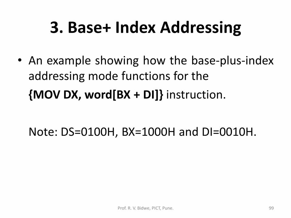
3. Base+ Index Addressing
• An example showing how the base-plus-indexaddressing mode functions for the
{MOV DX, word[BX + DI]} instruction.
Note: DS=0100H, BX=1000H and DI=0010H.
99Prof. R. V. Bidwe, PICT, Pune.

100Prof. R. V. Bidwe, PICT, Pune.

4. Base+ Index+ Displacement Addressing
• Similar to base-plus-index addressing anddisplacement addressing.– Data in a segment of memory are addressed by
adding the displacement to the contents of abase or an index register (BP, BX, DI, or SI)
• Figure shows the operation of the
{MOV AX, word[BX+1000H]} instruction.
when BX=0100H and DS=0200H
101Prof. R. V. Bidwe, PICT, Pune.

• The operation of the
{MOV AX, word[BX+1000H]} instruction.
102Prof. R. V. Bidwe, PICT, Pune.

Implied/ Implicit Addressing Mode
• Instructions with no oprand belongs to this addressing mode.
Prof. R. V. Bidwe, PICT, Pune. 103

Introduction to NasmHello World: 64 BitSection .datamsg: db "HELLO!",0x0Alen: equ $-msg
Section .textglobal mainmain:
mov rax, 1mov rdi, 1mov rsi, msgmov rdx, lenSyscall
mov rax, 60mov rdi, 0syscall
Prof. R. V. Bidwe, PICT, Pune. 104
Hello World: 32 BitSection .datamsg: db "HELLO WORLD",10len: equ $-msg
Section .textglobal mainmain:
mov eax, 4mov ebx, 1mov ecx, msgmov edx, lenint 0x80
mov eax, 1mov ebx, 0int 0x80

1. Assembler
• TASM (Windows) ::: 16 bit
• MASM (Windows) ::: 64 bit
• NASM (Linux) ::: 64 bit
2. Different buses used of processor
• Data bus : Defines Bandwidth.
• Address bus : Defines size of Physical Memory.
105Prof. R. V. Bidwe, PICT, Pune.

3. Register File
106Prof. R. V. Bidwe, PICT, Pune.

4. NASM program template
section .data
; Predefine Data [Variable definition]
section .bss
; Undefined Data [Variable declaration]
section .textglobal mainmain:
; Source code
Mov rax,60 ; Exit system callMov rdi, 00syscall
107Prof. R. V. Bidwe, PICT, Pune.
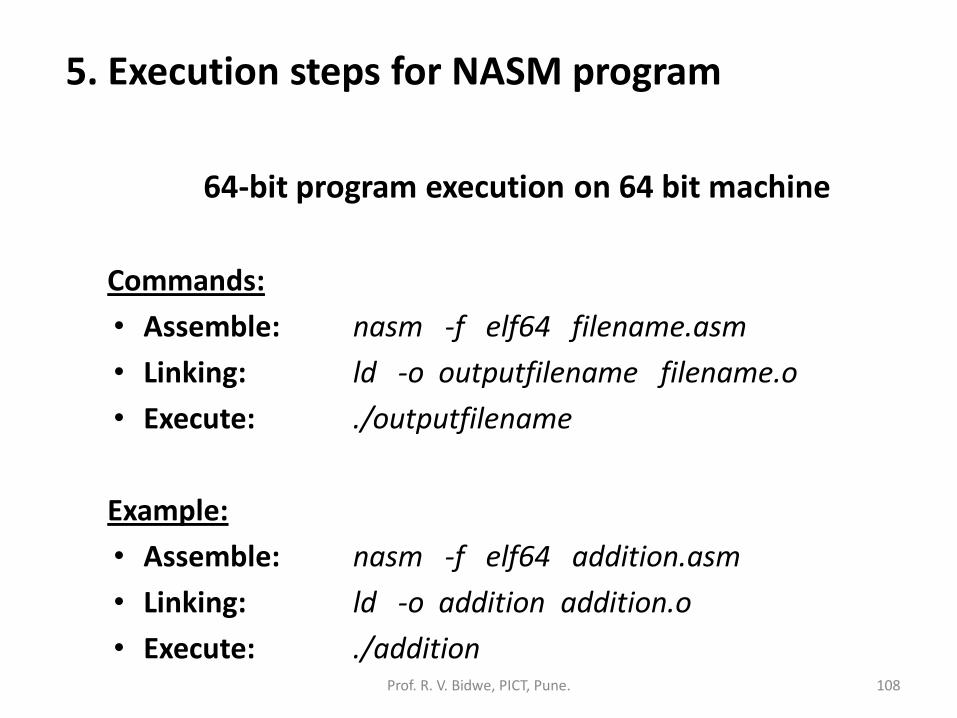
5. Execution steps for NASM program
64-bit program execution on 64 bit machine
Commands:
• Assemble: nasm -f elf64 filename.asm
• Linking: ld -o outputfilename filename.o
• Execute: ./outputfilename
Example:
• Assemble: nasm -f elf64 addition.asm
• Linking: ld -o addition addition.o
• Execute: ./addition108Prof. R. V. Bidwe, PICT, Pune.

5. Execution steps for NASM program
32-bit program execution on 32 bit machine
Commands:
• Assemble: nasm -f elf filename.asm
• Linking: ld -o outputfilename filename.o
• Execute: ./outputfilename
Example:
• Assemble: nasm -f elf addition.asm
• Linking: ld -o addition addition.o
• Execute: ./addition109Prof. R. V. Bidwe, PICT, Pune.

5. Execution steps for NASM program
32-bit program execution on 64 bit machine
Commands:
• Assemble: nasm -f elf filename.asm
• Linking: ld –m elf_i386 –o outputfilenamefilename.o
• Execute: ./outputfilename
Example:
• Assemble: nasm -f elf64 addition.asm
• Linking: ld -m elf_i386 -o addition addition.o
• Execute: ./addition
110Prof. R. V. Bidwe, PICT, Pune.

1. Basic Data Types
Data Types:
• Byte (8-bit)
• Word (16-bit)
• Double word (32-bit)
• Quadword (64-bit)
• Ten bytes (80-bit)
111Prof. R. V. Bidwe, PICT, Pune.
ALP Constructs

2. Data Types
1. Definition directives
• db (define byte)
• dw (define word)
• dd (define double word)
• dq (define quad word)
• dt (define ten bytes)
2. Declaration directives
• resb (reserve byte)
• resw (reserve word)
• resd (reserve double word)
• resq (reserve quad word)112Prof. R. V. Bidwe, PICT, Pune.

3. Memory addressing directives
• byte
• word
• dword
• qword
Prof. R. V. Bidwe, PICT, Pune. 113

3. Byte Ordering in Computer Memory (Data definition)
1. Little endian machine
• Stores data little-end first
• Least significant byte at smallest address
• Example: Intel processors (all x86 processors)
2. Big endian machine
• Stores data big-end first
• Most significant byte at smallest address
• Example: IBM processors (Power PC)
114Prof. R. V. Bidwe, PICT, Pune.

4. Byte Ordering in Computer Memory – Data Definition (Continued…)
Little endian Big endian
Qnumber dq 12345678A95CCDFE h
Memory
location
Data
1000000A h
10000009 h 12
10000008 h 34
10000007 h 56
10000006 h 78
10000005 h A9
10000004 h 5C
10000003 h CD
10000002 h FE
10000001 h
10000000 h
Memory
location
Data
1000000A h
10000009 h FE
10000008 h CD
10000007 h 5C
10000006 h A9
10000005 h 78
10000004 h 56
10000003 h 34
10000002 h 12
10000001 h
10000000 h
115Prof. R. V. Bidwe, PICT, Pune.

5. Memory addressing
section .data
num dq 9828919849096878h
section .bss
name resb 8 ; assembly
Memory addressing:
mov al, byte[num] ; al = 78
mov ax , word [num] ; ax = 6878
mov eax , dword [num] ; eax = 49096878
mov rax , qword [num]
; rax = 9828919849096878
Memory location Data
1000000A h
10000009 h 9810000008 h 2810000007 h 9110000006 h 9810000005 h 4910000004 h 0910000003 h 6810000002 h 7810000001 h
10000000 h
116Prof. R. V. Bidwe, PICT, Pune.

6. System calls 32-bit
Syntax:
mov eax, syscall number ;03-read, 04-write, 01-exit
mov ebx, file descriptor ;01 – standard input/output e.g. console
mov ecx, buffer ;buffer to be read / written
mov edx, length in bytes ;number of bytes to read / write
int 0x80
117Prof. R. V. Bidwe, PICT, Pune.

6. System calls 64-bit
Syntax:
mov rax, syscall number ;00-read, 01-write, 60-exit
mov rdi, file descriptor ;01 – standard input/output e.g. console
mov rsi, buffer ;buffer to be read / written
mov rdx, length in bytes ;number of bytes to read / write
syscall
118Prof. R. V. Bidwe, PICT, Pune.

6. System calls (Continued..)
Example: Write system call
64 bit 32bit
mov rax, 01 mov eax, 04
mov rdi, 01 mov ebx, 01
mov rsi, name mov ecx, name
mov rdx, 8 mov edx, 8
syscall int 0x80
119Prof. R. V. Bidwe, PICT, Pune.

6. System calls (Continued..)
Example: Read system call
64 bit 32bit
mov rax, 00 mov eax, 03
mov rdi, 01 mov ebx, 01
mov rsi, name mov ecx, name
mov rdx, 8 mov edx, 8
syscall int 0x80
120Prof. R. V. Bidwe, PICT, Pune.

6. System calls (Continued..)
Example: Exit system call
64 bit 32bit
mov rax, 60 mov eax, 01
mov rdi, 00 mov ebx, 00
syscall int 0x80
121Prof. R. V. Bidwe, PICT, Pune.

7. ‘Hex to ASCII’ & ‘ASCII to Hex’ conversion
122Prof. R. V. Bidwe, PICT, Pune.


![[Lecture-07] the Thumb Instruction Sets](https://static.fdocuments.in/doc/165x107/577ce06b1a28ab9e78b34814/lecture-07-the-thumb-instruction-sets.jpg)