Unit 3 8255 PPI - · PDF file8255 Programmable Peripheral Interface –PPI Has 24 I/O pins...
35
Unit 3 8255 PPI
Transcript of Unit 3 8255 PPI - · PDF file8255 Programmable Peripheral Interface –PPI Has 24 I/O pins...
Unit 3
8255 PPI

8255
Programmable Peripheral Interface – PPI
Has 24 I/O pins
Two 8-bit parallel ports : A and B.
Remaining eight pins: Port C
Eight pins can be grouped into two 4-bit as Cupper(CU) andClower (CL) or used as individual
The functions of these ports are defined by writing control wordto the control register.
Remember: it is a general purpose I/O device that is used withalmost any microprocessor.

8255 Operates in two modes
Bit set/Reset mode
I/O mode
BSR used to set or reset bits of port C
I/O mode divided into 3 modes:
Mode 0
Mode 1
Mode 2
Mode 0: All ports are simple I/O
Mode 1: Handshake where A and B can use bits from port C ashandshake signals. In this mode two types of handshake are possible:interrupt or status check.
Mode 2: Port A can be used as bidirectional data transfer using signalsfrom C and port B can be used in mode 0 or mode1.

Block Diagram of 8255

Control Logic Has six lines:-
RD : Enables Read operation. When low MPU reads data from selected I/O port of 8255.
WR : Enables Write operation. When low MPU writes into selected I/O port or control register of 8255
RESET: Active high signal, clears control register and sets all ports to input mode.
CS, A0 and A1 : Device select signals
CS : Master chip select. Connected to decoded address
A0 and A1: connected too A0 and A1 of MPU address lines.
They together specify the I/O ports of the control register.
CS A1 A0 Selected
0 0 0 Port A
0 0 1 Port B
0 1 0 Port C
0 1 1 Control Register
1 X X 8255 not selected

Example of Chip select Logic
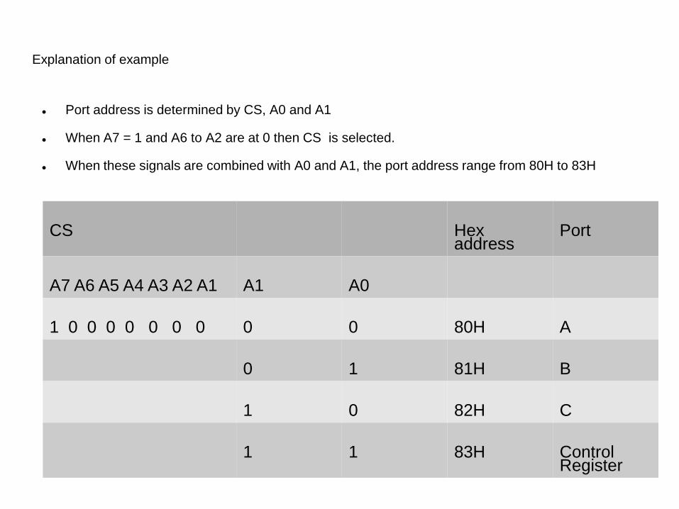
Explanation of example
Port address is determined by CS, A0 and A1
When A7 = 1 and A6 to A2 are at 0 then CS is selected.
When these signals are combined with A0 and A1, the port address range from 80H to 83H
CS Hex address
Port
A7 A6 A5 A4 A3 A2 A1 A1 A0
1 0 0 0 0 0 0 0 0 0 80H A
0 1 81H B
1 0 82H C
1 1 83H Control Register
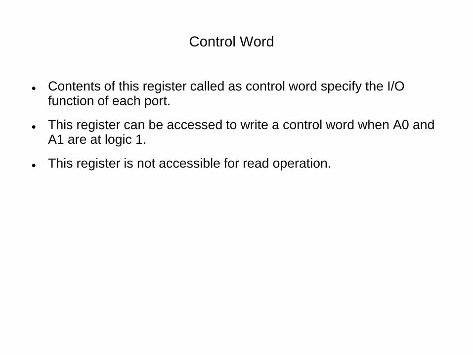
Control Word
Contents of this register called as control word specify the I/O function of each port.
This register can be accessed to write a control word when A0 and A1 are at logic 1.
This register is not accessible for read operation.

Data bus buffer
* This is a tri state bidirectional buffer used to interface the 8255 to systemdata bus. Data is transmitted or received by the buffer on execution ofinput or output instruction by the CPU.
* Control word and status information are also transferredthrough this unit.

Points to remember:
In order to coomunicate peripherals through 8255, three steps are necessary:
Determine the port and control register addresses according to the Chip select logic and address lines A0 and A1.
Write control word in the control register.
Write I/O instructions to communicate with the peripherals through ports A, B and C.
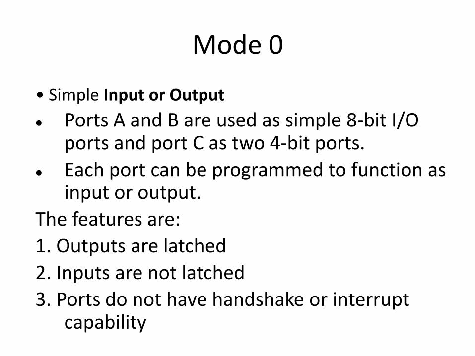
Mode 0
• Simple Input or Output
Ports A and B are used as simple 8-bit I/O ports and port C as two 4-bit ports.
Each port can be programmed to function as input or output.
The features are:
1. Outputs are latched
2. Inputs are not latched
3. Ports do not have handshake or interrupt capability

An example1. For the figure, determine the port address
and control register address2. Calculate the control word for mode 0 where port A is in and port CU are output ports and port B and CL are input ports.
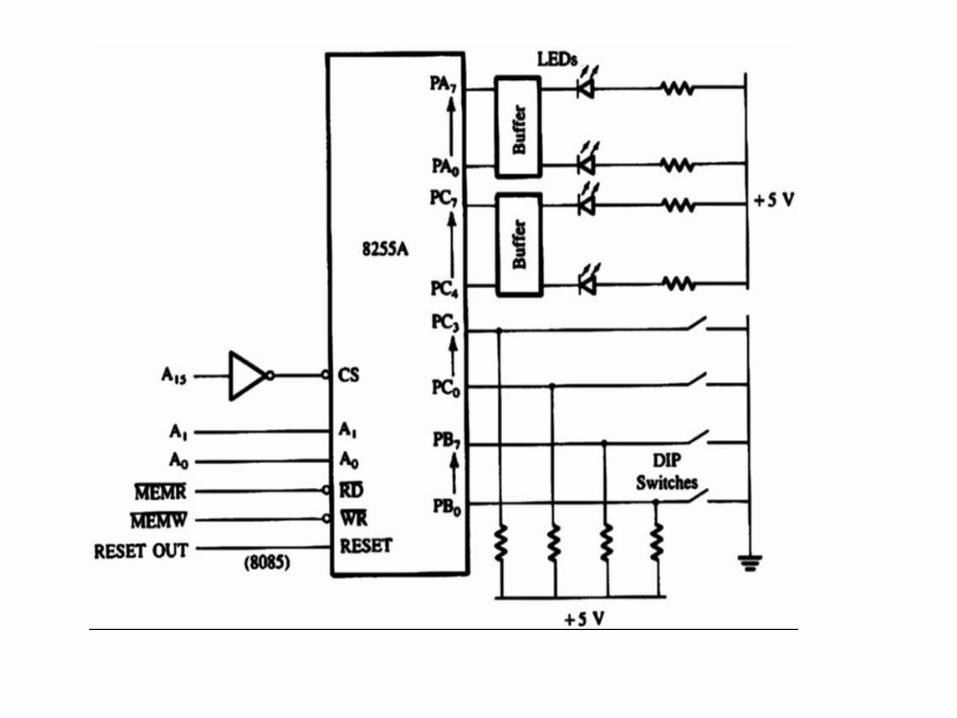

Ans 1: Port address
Since Chip select would occur when A15 is high and assuming all other don't care are at logic 0, the port address would be:
A15 A14...............A2 A1 A0
1 0000000000000 0 0 : 8000H : Port A
1 0000000000000 0 1 : 8001H : Port B
1 0000000000000 1 0 : 8002H : Port C
1 0000000000000 1 1 : 8003H : Control Register
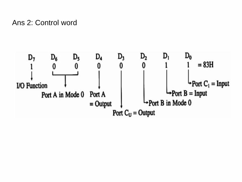
Ans 2: Control word

BSR ( Bit Set/Reset) mode
Mode concerned only with eight bits of port C.
Control word with D7 bit as 0 is recognised as BSR mode.
It does not alter previously transmitted control word.
So I/O operation of ports A and B remain unaffected by BSR control word.
In BSR mode, indiovidual bits of ports can be used for applications such as on/off.

Control word format in BSR is as followed
D7 D6 D5 D4 D3 D2 D1 D0
0 X X X S/R
BSR mode
Bit select
Bit select
Bit select
Set = 1Reset = 0
D6,D5,D4 generally set to 0D3,D2,D1 : 0 0 0 = bit 0
0 0 1 = bit 1 and so on.
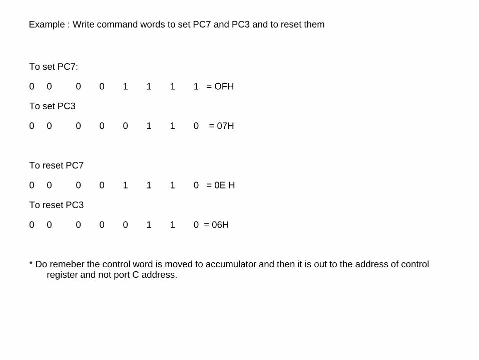
Example : Write command words to set PC7 and PC3 and to reset them
To set PC7:
0 0 0 0 1 1 1 1 = OFH
To set PC3
0 0 0 0 0 1 1 0 = 07H
To reset PC7
0 0 0 0 1 1 1 0 = 0E H
To reset PC3
0 0 0 0 0 1 1 0 = 06H
* Do remeber the control word is moved to accumulator and then it is out to the address of control register and not port C address.

Mode 1
Strobbed mode
Hand shake signals are exchanged between MPU and peripherals priorto the data transfer in this mode.
The features are:
Ports A and B function as 8-bit I/O ports. Can be configured as input oroutput.
Each port uses 3 lines from port C as handshake signals. The remainingtwo lines of port C can be used for simple I/O functions.
Input and Outputs are latched.
Interrupt logic is supported.
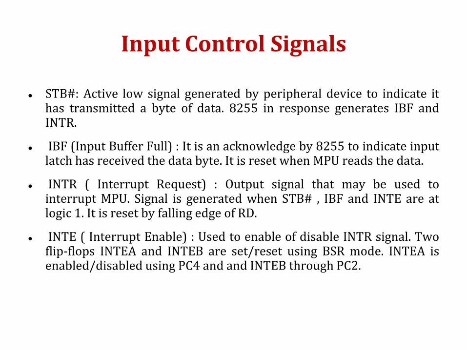
Input Control Signals
STB#: Active low signal generated by peripheral device to indicate ithas transmitted a byte of data. 8255 in response generates IBF andINTR.
IBF (Input Buffer Full) : It is an acknowledge by 8255 to indicate inputlatch has received the data byte. It is reset when MPU reads the data.
INTR ( Interrupt Request) : Output signal that may be used tointerrupt MPU. Signal is generated when STB# , IBF and INTE are atlogic 1. It is reset by falling edge of RD.
INTE ( Interrupt Enable) : Used to enable of disable INTR signal. Twoflip-flops INTEA and INTEB are set/reset using BSR mode. INTEA isenabled/disabled using PC4 and and INTEB through PC2.


Mode 1 ctd...
The diagram shows control signal for hankshaking where A and B are input ports. Port A uses
PC3,PC4 and PC5 where as Port B uses PC2, PC1 and PC0.
The control word is:
D7 D6 D5 D4 D3 D2 D1 D0
1 0 1 1 1/0 1 1 X
I/O mode
Port A mode 1
Port AMode 1
Port A input
PC6,7 1 = input0=output
Port B mode 1
Port B input
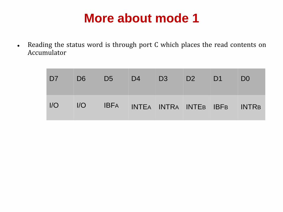
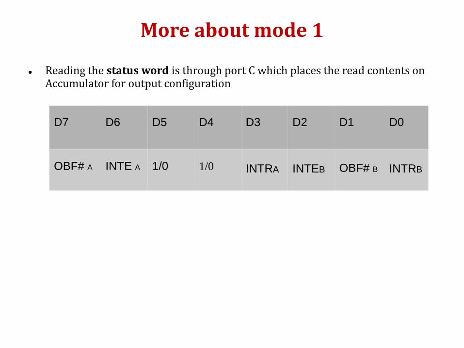
More about mode 1
Reading the status word is through port C which places the read contents onAccumulator
D7 D6 D5 D4 D3 D2 D1 D0
I/O I/O IBFA INTEA INTRA INTEB IBFB INTRB

Output control signals in mode 1
OBF# (Output Buffer Full) : Signal that goes low when MPU writes data into latch of8255. This indicates to an output peripheral that new data is ready to be read. It goeshigh after 8255 receives ACK from peripheral.
ACK# : Input from peripheral that must output a low when peripheral receives datafrom 8255 ports.
INTR ( Interrupt Request) : Output signal that is set by the rising edge of the ACK signal.This signal can be used to interrupt MPU to request the next data byte for output. INTR isset when OBF, ACK and INTE are one and is reset by falling edge of WR.
INTE ( Interrupt Enable) : Used to enable of disable INTR signal. Two flip-flops INTEA
and INTEB are set/reset using BSR mode. INTEA is enabled/disabled using PC6 and andINTEB through PC2.
PC4,5 : Can be used either as input or output.

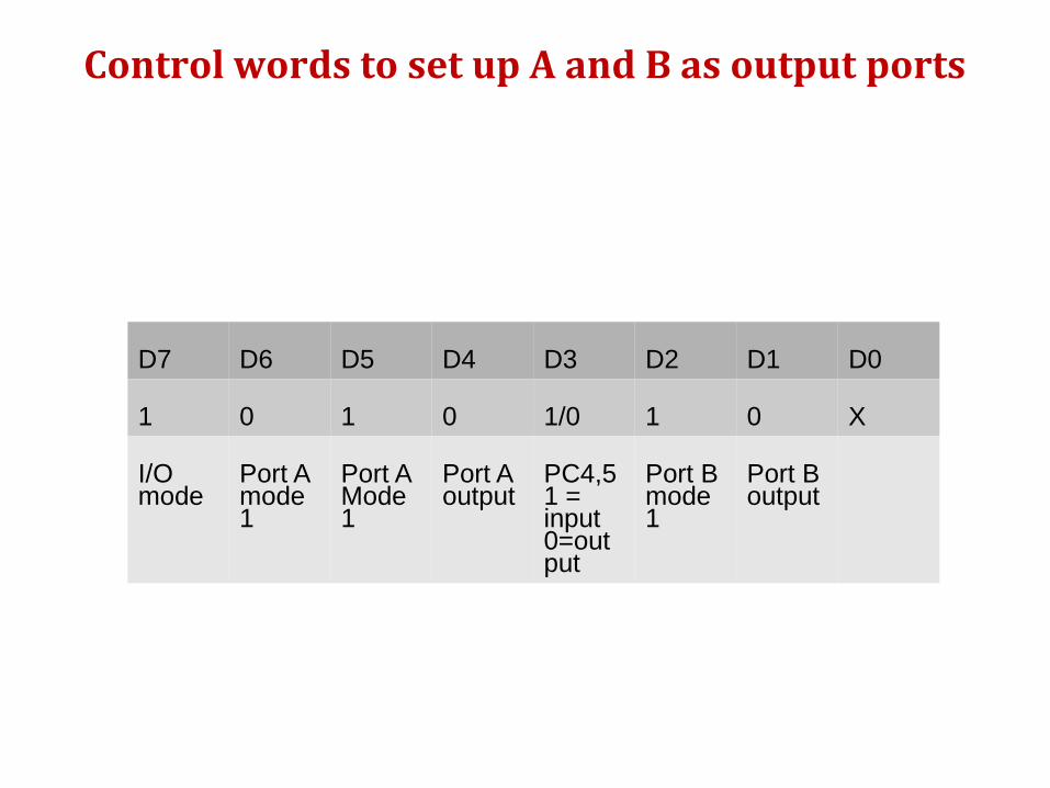
Control words to set up A and B as output ports
D7 D6 D5 D4 D3 D2 D1 D0
1 0 1 0 1/0 1 0 X
I/O mode
Port A mode 1
Port AMode 1
Port A output
PC4,5 1 = input0=output
Port B mode 1
Port B output
More about mode 1
Reading the status word is through port C which places the read contents on Accumulator for output configuration
D7 D6 D5 D4 D3 D2 D1 D0
OBF# A INTE A 1/0 1/0 INTRA INTEB OBF# B INTRB

Programming 8255 in Mode 1
Can be programmed as:
1. Status check
2. Interrupt I/O
In status check mode, the MPU continues to check data statusthrough IBF line until it goes high.
The disadvantage of status check I/O with handshake is that MPU istied in loop.

Applications of handshake????
For interfacing printer
For traffic light controller

Mode 2: Bidirectional data transfer
Port A as bidirectional and port B in 0 or 1.
Port A uses 5 signals form port C as handshake for data transfer.
Remaining three can either be I/O or handshake with B.

MODE 2 Control Signals
INTR : Interrupt request is an output thatrequests an interrupt.
~OBF : Output Buffer Full is an output indicatingthat that output buffer contains data for the bi-directional bus.
~ACK : Acknowledge is an input enablesperipheral to read data from 8255 port.
~STB : The strobe input loads data into the inputbuffer of 8255

IBF : Input buffer full is an output indicating thatthe input latch contains information for theexternal bi-directional bus.
INTE : Interrupt enable are internal bits thatenable the INTR pin. BIT PC6(INTE1) andPC4(INTE2).
PC2,PC1,PC0 : These port C pins are general-purpose I/O pins that are available for anypurpose.
MODE 2 Control Signals

Mode 2 Bi-directional Operation
•Timing diagram is a combination of the Mode 1 Strobed Input and Mode 1 Strobed Output Timing diagrams.

To summarize
8255 : PPI
8 bit 3 ports
I/O and BSR mode
I/O : 3 modes Simple I/O – mode 0, handshake – mode 1, bi-directional – mode 2.
Simple I/O: All the ports : input and output
Handshake: A and B I/O, each use 3 lines of port C for control signals.
Bi-directional: Only A. B can be used for mode 0 or 1. Port A uses 5 lines of C, remaining can be used as simple I/O or handshake with B.