RadioNet Engineering Forum Workshop : Next Generation Correlators for Radio Astronomy and Geodesy
Upload
truongtuyenCategory
view
213download
0
AS
TRO
N-F
O-0
17 2
.0
UniBoard2 R&D / DESP
Doc.nr.: ASTRON-RP-?? Rev.: 0.4 Date: 01-07-2014 Class.: Public
1 / 34
UniBoard2 HW Detailed Design
(draft)
Organisatie / Organization Datum / Date Auteur(s) / Author(s):
Gijs Schoonderbeek Sjouke Zwier ASTRON 17-06-2014
Controle / Checked:
ASTRON
Goedkeuring / Approval:
A.W. Gunst ASTRON
Autorisatie / Authorisation:
Handtekening / Signature
ASTRON
© ASTRON 2014 All rights are reserved. Reproduction in whole or in part is prohibited without written consent of the copyright owner.

UniBoard2 R&D / DESP
Doc.nr.: ASTRON-RP-?? Rev.: 0.4 Date: 01-07-2014 Class.: Public
2 / 34
Distribution list: Group: Others:
Andre Gunst Eric Kooistra Sjouke Zwier Daniël van der Schuur UniBoard2
Document history: Revision Date Chapter / Page Modification / Change
0.1 07-01-2014 Schoonderbeek Creation
0.2 10-02-2014 Schoonderbeek First release to wiki
0.3 17-06-2014 Schoonderbeek Adjust for schema review
0.4 01-07-2014 Schoonderbeek Adjust for review
UniBoard2 R&D / DESP
Doc.nr.: ASTRON-RP-?? Rev.: 0.4 Date: 01-07-2014 Class.: Public
3 / 34
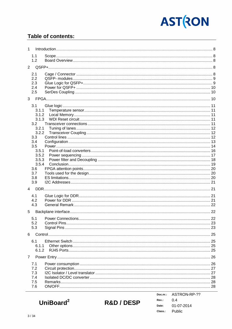
Table of contents:
1 Introduction ........................................................................................................................................... 8
1.1 Scope ........................................................................................................................................... 8 1.2 Board Overview ............................................................................................................................ 8
2 QSFP+.................................................................................................................................................. 8
2.1 Cage / Connector ......................................................................................................................... 8 2.2 QSFP- modules ............................................................................................................................ 9 2.3 Glue Logic for QSFP+ ................................................................................................................... 9 2.4 Power for QSFP+ ....................................................................................................................... 10 2.5 SerDes Coupling ........................................................................................................................ 10
3 FPGA .................................................................................................................................................. 10
3.1 Glue logic ................................................................................................................................... 11 3.1.1 Temperature sensor ................................................................................................................ 11 3.1.2 Local Memory ......................................................................................................................... 11 3.1.3 WDI Reset circuit .................................................................................................................... 11
3.2 Transceiver connections ............................................................................................................. 11 3.2.1 Tuning of lanes ....................................................................................................................... 12 3.2.2 Transceiver Coupling .............................................................................................................. 12
3.3 Control lines ............................................................................................................................... 12 3.4 Configuration .............................................................................................................................. 13 3.5 Power ......................................................................................................................................... 14
3.5.1 Point-of-load converters .......................................................................................................... 16 3.5.2 Power sequencing .................................................................................................................. 17 3.5.3 Power filter and Decoupling .................................................................................................... 18 3.5.4 Conclusion .............................................................................................................................. 19
3.6 FPGA attention points ................................................................................................................. 20 3.7 Tools used for the design ............................................................................................................ 20 3.8 ES limitations .............................................................................................................................. 20 3.9 I2C Addresses ............................................................................................................................ 21
4 DDR.................................................................................................................................................... 21
4.1 Glue Logic for DDR ..................................................................................................................... 21 4.2 Power for DDR ........................................................................................................................... 21 4.3 General Remark ......................................................................................................................... 22
5 Backplane interface............................................................................................................................. 22
5.1 Power Connections ..................................................................................................................... 22 5.2 Control Pins ................................................................................................................................ 23 5.3 Signal Pins ................................................................................................................................. 23
6 Control ................................................................................................................................................ 25
6.1 Ethernet Switch .......................................................................................................................... 25 6.1.1 Other options .......................................................................................................................... 25 6.1.2 RJ45 Ports .............................................................................................................................. 25
7 Power Entry ........................................................................................................................................ 26
7.1 Power consumption .................................................................................................................... 26 7.2 Circuit protection ......................................................................................................................... 27 7.3 I2C Isolator / Level translator ...................................................................................................... 27 7.4 Isolated DC/DC converter ........................................................................................................... 28 7.5 Remarks ..................................................................................................................................... 28 7.6 ON/OFF ...................................................................................................................................... 28

UniBoard2 R&D / DESP
Doc.nr.: ASTRON-RP-?? Rev.: 0.4 Date: 01-07-2014 Class.: Public
4 / 34
8 Clock and Sync ................................................................................................................................... 28
9 Test strategy ....................................................................................................................................... 29
9.1.1 Boundary scan ........................................................................................................................ 29 10 PCB ............................................................................................................................................... 30
10.1.1 Remarks ............................................................................................................................. 31
11 Green ............................................................................................................................................. 31
12 Board layout ................................................................................................................................... 32
List of figures: Figure 1 Concept 3 Single Column ............................................................................................................... 8Figure 2 1x3 zQSFP+ cage (left) and belly-to-belly orrientation (right) ........................................................... 9Figure 3 Recommended power supply filter ................................................................................................ 10Figure 4 Plane cutouts for coupling capacitors. ........................................................................................... 12Figure 5 Configuration setup ...................................................................................................................... 13Figure 6 Arria10 Power supply tree for data rates between 11.3 and 17.4Gbps .......................................... 14Figure 7 Power sequencing ........................................................................................................................ 14Figure 8 Altera Power Manager Implementation ......................................................................................... 16Figure 9 Simple sequencer ........................................................................................................................ 17Figure 10 Power Sequencing of UniBoard2 ................................................................................................. 18Figure 11 FPGA power scheme ................................................................................................................. 20Figure 12 Power connectors ....................................................................................................................... 23Figure 13 Picture of backplane connectors ................................................................................................. 24Figure 14 UniBoard control ........................................................................................................................ 25Figure 15 UniBoard Power tree .................................................................................................................. 26Figure 16 ON/OFF latching pushbutton ...................................................................................................... 28Figure 17 Boundary scan overview ............................................................................................................. 30Figure 18 Layer stack ................................................................................................................................. 30Figure 19 Overview of UniBoard2 ............................................................................................................... 33Figure 20 Board set-up with FPGA-to-FPGA interconnections .................................................................... 34 List of tables: Table 1 QSFP+ Cages ................................................................................................................................ 9Table 2 QSFP+ connectors .......................................................................................................................... 9Table 3 QSFP+ modules .............................................................................................................................. 9Table 4 QSFP+ control signals ..................................................................................................................... 9Table 5 Aria 10, GX1150 Specifications ..................................................................................................... 10Table 6 I2C temperature sensors ............................................................................................................... 11Table 7 I2C EEPROMs .............................................................................................................................. 11Table 8 WDI devices .................................................................................................................................. 11Table 9 Used transceiver channels of the FPGA. ....................................................................................... 12Table 10 Transceiver options ..................................................................................................................... 12Table 11 Control interfaces ........................................................................................................................ 12Table 12 Serial Configuration devices ........................................................................................................ 13Table 13 FPGA power supplies .................................................................................................................. 15Table 14 EPE results ................................................................................................................................. 15Table 15 Point of Load Converters ............................................................................................................. 16

UniBoard2 R&D / DESP
Doc.nr.: ASTRON-RP-?? Rev.: 0.4 Date: 01-07-2014 Class.: Public
5 / 34
Table 16 POL selection .............................................................................................................................. 16Table 17 Ferrite Beads ............................................................................................................................... 19Table 18 Decoupling Scheme .................................................................................................................... 19Table 19 I2C addresses ............................................................................................................................. 21Table 20 DDR4 power supplies .................................................................................................................. 21Table 21 Backplane connector power pin's. ................................................................................................ 22Table 22 Power connector options ............................................................................................................. 22Table 23 Control pins needed on the backplane. ........................................................................................ 23Table 24 Backplane connector power pin's. ................................................................................................ 23Table 25 Signal connector options ............................................................................................................. 24Table 26 Impact part numbers .................................................................................................................... 24Table 27 Switch options ............................................................................................................................. 25Table 28 RJ45 Control connector selection ................................................................................................ 26Table 29 UniBoard Power estimation ......................................................................................................... 27Table 30 Hot swap controllers .................................................................................................................... 27Table 31 I2C Isolators ................................................................................................................................ 27Table 32 Isolated DC/DC converters .......................................................................................................... 28Table 33 LVDS and LVPECL levels ............................................................................................................ 28Table 34 Clock fanout buffers ..................................................................................................................... 29Table 35 Overview Test strategy ................................................................................................................ 29Table 36 JTAG Signal levels ...................................................................................................................... 29Table 37 Lattice Semiconductor FPGA/CPLD options ................................................................................ 30Table 38 Estimates layer according Altera .................................................................................................. 31 Terminology: bps Bits per second BCK Backplane BW BandWidth Clk Clock DDR Double Data Rate DC Direct Current DC/DC DC tot DC converter EEPROM Electrical Erasable Program Read only Memory EMI Electro-Magnetic Interference ETH Ethernet ES Engineering Sample FD Full Duplex Firmware Embedded or real-time code that runs on a microprocessor (e.g. written in C) FPGA Field Programmable Gate Array Hardware Boards, subracks and COTS equipment HMC Hybrid Memory Cube I2C Serial communication bus between chip (Inter IC Bus) IO Input Output IP Intellectual Property IPC Association Connecting Electronics Industries (formally Institute for Interconnecting and
Packaging Electronic Circuits) JTAG Joint Test Action Group (protocol for Boundary scan) LDO Low DropOut regular LVTTL Low Voltage TTL (Transistor Transistor Logic) PCB Printed Circuit Board PMBus Power Management Bus (I2C interface to control Power modules) POL Point of Load PPS Pulse per Second PDN Power Distribution Network

UniBoard2 R&D / DESP
Doc.nr.: ASTRON-RP-?? Rev.: 0.4 Date: 01-07-2014 Class.: Public
6 / 34
PHY physical interface (layer 1 of OSI model) QSFP Quad Small Form factor Pluggable RAM Right Angle Module RF Radio Frequency RoHS Reduction of Hazardous Substances SFP+ SFP for 10GbE SerDes Serializer Deserializer SNMP Simple Network Management Protocol SODIMM Small Outline Dual Inline Memory Module SSO Simultaneous Switching Noise SPD Serial Present Detection TAP Test Access Point WDI Watch Dog Interrupt XFP 10G Small form-factor Pluggable transceiver

UniBoard2 R&D / DESP
Doc.nr.: ASTRON-RP-?? Rev.: 0.4 Date: 01-07-2014 Class.: Public
7 / 34
References: [1] Deliverable 8.2 UniBoard2 Hardware Design Document, Astron, Gijs Schoonderbeek, 07-10-2013,
ASTRON-TN-040 1.0 3 [2] 1x3 Cage Assembly, zQSFP+, TE, ENG_CD_2173239_A [3] Datasheet AFBR-79EQDZ 40Gigabit Ethernet & Infiniband QSFP+ Pluggable, Parallel Fiber-Optics
Module, Avago Technologies, AV02-2924EN January 28, 2013 [4] Arria 10 Device Overview, Altera Corp., AIB-01023, 2013.09.04 [5] DDR4 and GDDR5M SODIMM 256 Pin Socket 0.5mm Pitch, JEDEC, SO-018, October 2012 [6] DDR4 SDRAM SODIMM MTA18ASF1G72Hz – 8GB, Micron Technology Inc., asf18C1gx72hz Rev A
10/13 EN [7] VSC7389 SparX-G16 16-Port Integrated Layer-2 Gigabit Ethernet Smart Swtich with Transceivers
datasheet, Vitesse Corp. Rev. 2.4 December 2006 [8] PIC18F97J60 Family Data Sheet, Micorchip, 2011, DS39762F [9] PIC32MX5XX/6XX/7XX 32-bit Microcontrollers, Microchip 2009-2013, DS60001156H [10] TransceiverLink Design Guidelines for High-Gbps Data Rate Transmission, AN-672, 2013.02.15. Altera
Corp. [11] PCB Stackup Design Considerations for Altera FPGAs, AN-613, version 1.0, October 2010 Altera Corp. [12] Via Optimization Techniques for High-Speed Channel Designs, AN-529, version 1.0,May 2008, Altera
Corp. [13] Printed Circuit Board (PCB) Power Delivery Network (PDN) Design Methodology, AN574, May 2009,
Altera Corp [14] Power Management in Arria 10 Devices, Altera Corp. A10-PWR 2013.12.02 [15] Remote Sensing for power supplies, Texas Instruments, 2Q 2012 [16] PMBus Power System Management Protocol Specifications Part II – Command Language, Power SIG,
Revision 1.1, 5 February 2007 [17] Clock Networks and PLLs in Arria 10 Devices, A10-CLKPLL, Altera Corp. 2013.12.02 [18] Reduce Your PCB Costs With Blind Vias, Buried Vias & Microvias, Pi Zhang, Nuvation Engineering,
EDN 02/03/2014, [19] Datasheet Micron Serial NOR Flash Memory N25Q00AA, Micron Technology Inc. [20] EPCQ-L Serial Configuration Devices Datasheet, Altera Corp. 2014.06.17 [21] Configuration, Design Security and Remote System Upgrades in Arria 10 Devices, A10-CONFIG, Altera
Corp, 2013.12.02 [22] Arria 10 Device Datasheet, Altera Corp. A10-Datasheet-2013.12.06 [23] Arria 10GX, GT and SX device Family Pin Connection Guidelines, PCG-01017-1.1, Altera Corp, ver. 1.1
18-12-2013

UniBoard2 R&D / DESP
Doc.nr.: ASTRON-RP-?? Rev.: 0.4 Date: 01-07-2014 Class.: Public
8 / 34
1 Introduction
1.1 Scope In this document the detailed hardware design for UniBoard2 is described [1]. Details about the extension board including the HMC are described in a separate document. The goal of this document is to make all design choices at forehand before the schematic and PCB design takes place. UniBoard2 is a Joint Research Activity (JRA) in the RadioNet3 project, funded by the EC through the FP7 programme, under grant agreement no. 283393. The partners in this JRA are the Universities of Bordeaux and Orleans, INAF, MPG Bonn, the University of Manchester, ASTRON and JIVE.
1.2 Board Overview In the architecture document [1] the architecture with a single column of FPGA and all transceivers to the outside of the board was chosen. The overview of the board is repeated in Figure 1.
FPGA
QSFP
QSFP
QSFP
QSFP
FPGA
FPGA
FPGA
ETH Switch
4x4 RJ45 DC/DC
BCK
3x16 FD pairs for HMC6x4 FD pairs @10- 25Gbps
BCK
DDR4 SODIMM
DDR4 SODIMM
1-10GbE
DDR4 SODIMM
DDR4 SODIMM
DDR4 SODIMM
DDR4 SODIMM
DDR4 SODIMM
DDR4 SODIMM
4x1-10GbE
QSFPQSFP
QSFP
QSFP
QSFP
QSFP
QSFPQSFP
QSFP
QSFP
QSFP
QSFP
QSFPQSFP
QSFP
QSFP
QSFP
QSFP
QSFPQSFP
240-600Gbps FD
6x4 FD pairs @10- 25Gbps240-600Gbps FD
6x4 FD pairs @10- 25Gbps240-600Gbps FD
6x4 FD pairs @10- 25Gbps240-600Gbps FD
UniBoard2
BCK
BCK
BCK
BCK
BCK
BCK
24 FD pairs for Mesh
3x16 FD pairs for HMC24 FD pairs for Mesh
3x16 FD pairs for HMC24 FD pairs for Mesh
3x16 FD pairs for HMC24 FD pairs for Mesh
Figure 1 Concept 3 Single Column
2 QSFP+ At the input of every FPGA on UniBoard2 six zQSFP+ cages will be placed, 3 on the top and 3 on the bottom of the board (belly-to-belly). In Figure 2 images of the zQSFP+ cages are shown. By using zQSFP+ cages instead of standard QSFP+ cages the speed can be increased from 10Gbps to 25Gbps. Although on the proto type op UniBoard2 an Arria10 GX device will be used, with only transceivers up to 17 Gbps, the transceivers will be connected to pair which can handle 28Gbps when an Arria 10 GT device is placed.
2.1 Cage / Connector To enable 100GbE interfaces (with Stratix 10 in mind) a 25Gb enabled QSFP28 cage (incl. Connector) will be placed on UniBoard2. An example is shown in Figure 2, taken from [2].

UniBoard2 R&D / DESP
Doc.nr.: ASTRON-RP-?? Rev.: 0.4 Date: 01-07-2014 Class.: Public
9 / 34
Figure 2 1x3 zQSFP+ cage (left) and belly-to-belly orrientation (right)
In Table 1 cages and in Table 2 connectors options are shown.
Table 1 QSFP+ Cages
Part number Manf. Specification 2173239-1 TE 1x3 cage (for belly-to-belly 111118-1520 Molex 1x4 cage U90-A321-1001 Amphenol
Table 2 QSFP+ connectors
Part Numbe Manf. Specification 170432-0002 Molex Mates with 111118-1520 1551920-2 TE FS1-X38-20M0-10 Amphenol
For UniBoard2 the TE combination will be used (belly-to-belly).
2.2 QSFP- modules In Table 3 a number options for modules are shown.
Table 3 QSFP+ modules
Part Number Manf. Specification AFBR-79EQDZ Avago 40Gigabit Ethernet FTL410QD2C Finisar 40Gigibit 300m
The module itself will not be part of the UniBoard2, but the specifications of the Avago module will be used for the design of UniBoard2.
2.3 Glue Logic for QSFP+ The control lines of an Avago AFBR-79EQDZ [3] QSFP+ module are taken as starting point for the design. The I2C control interface of each module will be connected to the FPGA. In Table 4 the control lines are shown.
Table 4 QSFP+ control signals
Signal Description Level Connection SCL Serial Clock 3.3V LVTTL To FPGA SDA Serial Data 3.3V LVTTL To FPGA ModSelL Module Select 3.3V LVTTL Pull low LPMode Low Power Mode 3.3V LVTTL Pull low ModePresL Module Preset 3.3V LVTTL Res. Pull High (can be used to switch power on /
Module detection) RestL Module Reset 3.3V LVTTL With pull up to FPGA IntL Interrupt Open collector out Pull Up. (read out via control interface possible)

UniBoard2 R&D / DESP
Doc.nr.: ASTRON-RP-?? Rev.: 0.4 Date: 01-07-2014 Class.: Public
10 / 34
From this table it can be seen that 3 lines per cage are connected to the FPGA (with six cages in total 18 lines). Between the QSFP+-control and the FPGA a level converter is needed. An overview of level converters is shown in section 7.3
2.4 Power for QSFP+ For the power requirements for the QSFP+ the Avago AFBR-79EQDZ [3] will be taken as starting point. This module needs 3.3V with a maximal noise of 50mVpp. The max power consumption is 1.5W for a 40Gbps. For modules up to 100Gbps the power consumption can be increased to 3.5W. Given a 100Gbps modules, the power supply for the six cages should be 6.5A. Power supply options:
• Ericsson BRM461 4.5-14V input, 12A, 12.2x12.2mm, 96% efficiency Control and monitoring possible.
• Ericsson BRM463 4.5-14V input 25A, 1 module for 2/4 FPGAs
According Avago [3] the power input has to be filtered. An example is shown in Figure 3.
Figure 3 Recommended power supply filter
2.5 SerDes Coupling Because the FPGA uses 1.8V to power the SerDes channels and the QSFP+ 3V3, the DC level can be different. Therefore AC coupling will be used between the FPGA and the QSFP+ cage. The AC-coupling is done inside the optical module.
3 FPGA On UniBoard four Altera Arria 10 GX 1150 with part number 10AX115U4F4514SGES will be used. Some key specifications are shown in Table 5.
Table 5 Aria 10, GX1150 Specifications
Specification Specification Registers 1710800 Memory 53Mbits SerDes channels 96 Transceiver speed 17.4Gbps 18x18 Multipliers 3036 Pins 1932 Size 45x45mm

UniBoard2 R&D / DESP
Doc.nr.: ASTRON-RP-?? Rev.: 0.4 Date: 01-07-2014 Class.: Public
11 / 34
3.1 Glue logic
3.1.1 Temperature sensor
Although the temperature can be monitored with internal logic using the internal temperature sensing diode (TSD) and ADC [14], an external sensor will be placed next to each individual FPGA as well. In Table 6 an overview of I2C sensors is shown.
Table 6 I2C temperature sensors
Type Manf. Supply Voltage Package JTAG model Availability NCT203 On Semiconductor 1.4-2.75V - - TS3000GB0A0 IDT 1.7-1.9V TDFN8 - - STTS3000 ST 2.3-3.6V TDFN8 - - STLM75M2E STMicroelectronics 2.7-5.5V SO-8 - OK MAX31725 Maxim 2.7-3.7V TDFN8 - OK MAX1619 Maxim 3.0V 16QSOP ok OK ADT7411 Analog Devices 2.7-5.5V 16QSOP ok OK LM99 Ti 3.0-3.6V VSSOP-8 - OK TMP451 Ti 1.7-3.6 8 WSON - Mouser
On UniBoard2 the TMP451 will be used.
3.1.2 Local Memory
To enable storage of local variable a small I2C memory can be placed next to the FPGA. In Table 7 an overview of storage device is shown.
Table 7 I2C EEPROMs
Type Manf. Supply Voltage Mem. Size JTAG model Availability 24VL014 Microchip Technology 1.5-3.6V 128x8 ok ok 24AA00 Microchip Technology 1.7-5.5V 6x8 24AA01 ok AT24C01C Atmel 1.7-5.5V 128x8 AT24C01b ok M24128 ST 2.5-5.5V 16kx8 - ok
The EEPROM will be placed on the same bus as the temperature sensor. They all have the same housing and pinning. For UniBoard2 the CAT24C02WI-G will be used as starting point.
3.1.3 WDI Reset circuit
Next to every FPGA a Supervisory / WDI will be placed. In Table 8 an overview of WDI circuits are shown.
Table 8 WDI devices
Type Manf. Supply Remark ADM8320 Analog Devices ADM811 Analog Devices Monitoring Used On UniBoard STM6823 STMicroelectr. Monitor
The STM6823 will be used. The reset circuit will be connected to the Power good of the sequencer.
3.2 Transceiver connections For UniBoard2 only transceiver interfaces will be used for data communication. In Table 9 an overview of the transceiver channels is given.

UniBoard2 R&D / DESP
Doc.nr.: ASTRON-RP-?? Rev.: 0.4 Date: 01-07-2014 Class.: Public
12 / 34
Table 9 Used transceiver channels of the FPGA.
Use Nof front side channels Use Nof back side channels QSFP+ 24 HS channels Backplane (HMC) 48 (3x16) 24 channels
The options for the remaining 24 transceivers are shown in Table 10.
Table 10 Transceiver options
Option Pro Con To backplane - Standard interfaces
- Flexible to use - Space on board needed (with 5
signal layer 24 transceivers, 6mm needed)
- Long traces, low speed Mesh - Comparable with UniBoard1
- Speed of mesh better - Complicated layout.
Ring - Simple layout (max. speed)
- Scalable for beamformer - Non standard interfaces
By replacing the Arria 10 GX device for a GT device 16 transceivers connected to the QSFP will increase in speed from 17Gbps to 28Gbps. A ring-architecture will be implemented on UniBoard2.
3.2.1 Tuning of lanes
The pairs within the RING will not be tuned lane-wise The pairs of the backplane will be tuned up to 800ps ~100mm (0.5*16UI of HMC lane-to-lane skew) The pairs for the QSFP will be tuned to 50mm.
3.2.2 Transceiver Coupling
The pairs for FPGA-to-FPGA are AC-coupled. Special care must be taken by placing the coupling capacitors [10]. Simulation will be done to analyse the optimal cut out (if any)
Figure 4 Plane cutouts for coupling capacitors.
The lowest frequency to couple is 10G/64 = 156.25MHz. This result in a capacitor of >20pF 100pF.
3.3 Control lines In Table 11 an overview of the different control lines per FPGA are shown.
Table 11 Control interfaces
Control interface Interface Type Number of line Logic levels QSFP+ I2C, control 6x2 + 5 3V3 Power Supply PMBus (I2C) 2 DDR I2C 2x2 Temperature / EEPROM I2C 2 1V8 Total: 25

UniBoard2 R&D / DESP
Doc.nr.: ASTRON-RP-?? Rev.: 0.4 Date: 01-07-2014 Class.: Public
13 / 34
3.4 Configuration For the FPGA a number of configuration schemes can be used [4]. For UniBoard the following starting points are taken:
- Minimal space, due to the number of power supplies needed to power the FPGA, PCB room is limited
- Remote reconfiguration - Possibility that all FPGAs can have a different image
Configuration time and partial configuration are not requirements for UniBoard2. UniBoard2 will therefore use the same schema as used on UniBoard, Active Serial Configuration (optionally with four lines to reduce configuration time) and configuration with JTAG for debug purposes. In Table 12 an overview of flash devices is shown.
Table 12 Serial Configuration devices
Part Number Manf. Size Width Power EPCQ256 Altera 256 Mbits 4 2.7-3.6 V EPCQ512 Altera 512 Mbits 4 2.7-3.6 V EPCQ-L512 Altera 512Mbits 4 1.8V EPCS128 Altera 128 Mbits 1 2.7-3.6 V MT25QU02 Micron 2Gbit 1/2/4 1.7-2.0V
Since both Altera and Micron devices have the same BGA package and pinning [19][20], an EPCQ-L1024 will be used as a start for the design. During proto typing a Micron device could be placed as well. The configuration size of the Arria 10 GX 1150 is 319kbit [22], this means that a 512Mbit device is sufficient for the Arria 10 FPGA. The configuration scheme is shown in Figure 5 [21]. By using a four wide bus for configuration the configuration time of UniBoard2 will be equal to UniBoard.
Figure 5 Configuration setup

UniBoard2 R&D / DESP
Doc.nr.: ASTRON-RP-?? Rev.: 0.4 Date: 01-07-2014 Class.: Public
14 / 34
3.5 Power For UniBoard2 switched converters can be used, this is in contrast with UniBoard where LDO where needed to power the transceiver parts of the FPGA. By using switched power supplies the efficiency of the power is increased, reducing the total power consumption. In Figure 6 the power tree of the FPGA as shown in [14] and [23] is repeated.
Figure 6 Arria10 Power supply tree for data rates between 11.3 and 17.4Gbps
Instead of using the power tree for the Arria 10 GX device, the power tree for the GT is used. By adding another power supply and splitting the VCCR_GXB and VCCT_GXB transceiver speeds up-to 28Gbps can be achieved with Arria10 GT. By using this circuit it is expected that when Arria 10’s are replaced by Stratix10 the full speed of the transceiver can be used. Not all power can be switched on at the same time, power supply sequencing is needed. The sequencing scheme as shown in Figure 7 is repeated from [Presentation Optimizing Power supply Design for Arria 10 Devices].
Figure 7 Power sequencing
A remark when VCC/VCCP differs from VCCT_GXB, VCCR_GXB and or VCCERAM group one has to be split in two. VCCBAT can be power any time. In Table 13 the power supplies for the FPGA are shown.

UniBoard2 R&D / DESP
Doc.nr.: ASTRON-RP-?? Rev.: 0.4 Date: 01-07-2014 Class.: Public
15 / 34
Table 13 FPGA power supplies
Signal Description Voltage ES extra EPE Expected VCC Core power supply 0.85-0.9 +10% 9 A 30A VCCERAM Memory Power
Pins 0.95 +/- 30mV
+30% 1.25 A 10A
VCCR_GXB Analog Power Receiver
1.0 +/- 30mV
+30% 8.5 A 10A
VCCT_GXB Analog Power Transmitter
1.0 +/- 30mV
+30% 2.2 A 5A
VCCBAT+VCCH_GXB Battery back-up 1.8V +30% 3.1 A 5A VCCIO (DDR) Memory 1.5V 1.3 A VCCIO IO 2.5V 0.8 A 2A The result of the EPE is shown in Table 14.
Table 14 EPE results
Power Supply Current (A)
Min Current Requirement (A)
User Mode Current Requirement (A)
Static Current (A)
Dynamic Current (A) Total Current (A)
ICC (0.9V, 0.8xV) 14.658 1.656 13.002 14.658 ICCP (0.9V, 0.8xV) 1.887 0.251 1.636 1.887 ICCA_FPLL (1.8V) 0.062 0.057 0.005 0.062 ICCIO ICCIO (1.5V) N/A 1.279 0.016 1.296 ICCIO (1.8V) N/A 0.000 0.005 0.005 ICCIO (2.5V) N/A 0.000 0.000 0.000 ICCIO (3.0V) N/A 0.000 0.000 0.000 ICCPT ICCPT (1.8V) N/A 0.844 0.064 0.908 ICCH_GXB (1.8V) 3.103 1.678 1.426 3.103 ICCR_GXB ICCR_GXB (0.9V) 8.518 3.386 5.131 8.518 ICCT_GXB ICCT_GXB (0.9V) 2.021 0.053 1.968 2.021 ICCPGM (1.8V) 0.000 0.000 0.000 0.000 ICCBAT (1.8V) 0.000 0.000 0.000 0.000 ICCERAM (0.9V) 1.245 0.033 1.212 1.245 ICCXCVR ICCHSSI 0.000 0.000 0.000 0.000 ICCHIP 0.000 0.000 0.000 0.000
As shown in the Altera WEBEX a Megafunction, supplied by Altera, can be used to readout the internal voltage and temperature to controls the powers accordingly, Figure 8.

UniBoard2 R&D / DESP
Doc.nr.: ASTRON-RP-?? Rev.: 0.4 Date: 01-07-2014 Class.: Public
16 / 34
Figure 8 Altera Power Manager Implementation
3.5.1 Point-of-load converters
For UniBoard2 DC/DC converters close to the FPGA, Point-Of-Load converters will be used. In Table 15 a number of options are shown.
Table 15 Point of Load Converters
Type Manf Output Voltage Max Current Size Remark BRM464 Ericsson 0.7-3.6V 40A 30.9x20.0mm TH/SMD, PMBus BMR462 Ericsson 0.6-5V 12A 21.0x12.7mm TH/SMD, PMBus BRM461 Ericsson 0.6-5V 12A 12.2x12.2mm TH/SMD, PMBus MDT040A0X3 GE Power 0.45-2.0 V 40A 30.0x13.5mm LGA, PMBus PDT003A0X3 GE Power 0.45-5.5V 3A 12.2x12.2mm LGA, PMBus UDXS1212A0X3 GE Power 0.48-5.5V 2x12A 20.3x11.4mm LGA, PMBus EN23F0Q1 Enpirion (Altera) 0.6-5V 15A 12x13mm No control, Chip EN2340Q1 Enpirion (Altera) 0.75-5.0 4A 8x11mm No control, Chip Although modules might take more space than Enpirion modules (for currents around 40A) a standard module will be used. These standard modules have more monitoring and control features than chips.
Table 16 POL selection
Topic Ericsson GE (Lineage Power) Mounting SMD / Through hole LGA Control PMBus PMBus SMBus level 3.0V 2.1V 40A running at 20A 0.9V ~87% ~85% Cap for ripple <20mVp-p, 1.8V
470uF (increase to 400kHz)
8x47uF
Default switch freq. 320kHz 400kHz On/Off pin CTRL (yes) Yes Remote Adjust PMBus PMBus # on single SMBus ~100 8 Remote sens In- Out voltage, output
current, Temp., Frequency, DC
In- Out voltage, output current, Temp, status
Selling feature Control / Software Tunable loop Availability Good Price indication
In section 7.3 and overview is given for device to translate the max 3.0V IO of the FPGA to the 3.3V logic of the power modules.

UniBoard2 R&D / DESP
Doc.nr.: ASTRON-RP-?? Rev.: 0.4 Date: 01-07-2014 Class.: Public
17 / 34
3.5.2 Power sequencing
For the new Altera Series sequencing of the power supplies are needed. For this the following parts can be used:
• LTC2978 Octal Digital Power Supply Manager. Program with EEPROM
• ADM1186 Analog Quad Voltage sequencer and monitor. Pro simple, working by design. Con monitoring missing (local power min. 3.3V, max. 5V)
• ADM1066 Super Sequencer with margining control. Pro monitoring, Con needs programming before use.
• PIC processor • MAX16025-16030, fixed thresholds (only up !) • LTC2928
Typical diagram is shown in Figure 9.
Figure 9 Simple sequencer
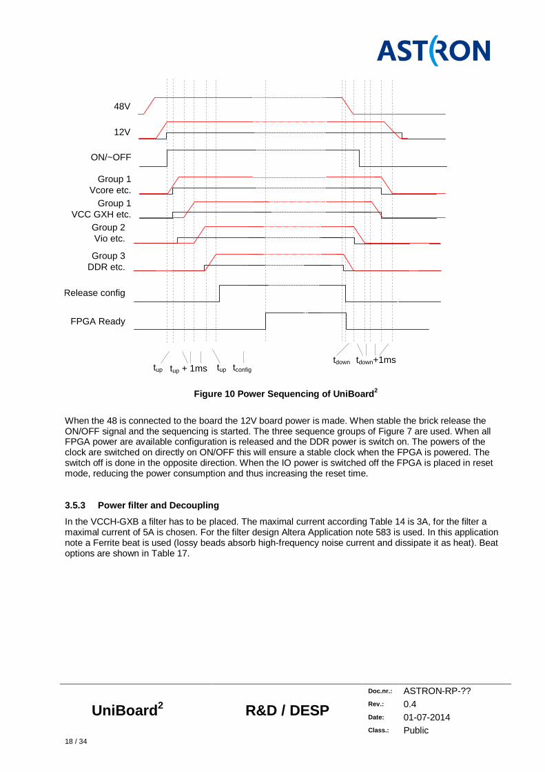
Although sequencing can be done on the POL modules a fail save simple sequencer is an easy solution and will be used on UniBoard2, this sequencer can be bypassed by the POL logic. The Sequencer will be power by the 5V LDO used for the DDR power supply. For this LDO is chosen to reduce component count. In Figure 10 an overview of the sequencing is shown.
UniBoard2 R&D / DESP
Doc.nr.: ASTRON-RP-?? Rev.: 0.4 Date: 01-07-2014 Class.: Public
18 / 34
Group 1Vcore etc.
Group 2Vio etc.
Group 3DDR etc.
ON/~OFF
Release config
FPGA Ready
48V
12V
tup tup + 1ms tconfigtdown tdown+1ms
tup
Group 1VCC GXH etc.
Figure 10 Power Sequencing of UniBoard2
When the 48 is connected to the board the 12V board power is made. When stable the brick release the ON/OFF signal and the sequencing is started. The three sequence groups of Figure 7 are used. When all FPGA power are available configuration is released and the DDR power is switch on. The powers of the clock are switched on directly on ON/OFF this will ensure a stable clock when the FPGA is powered. The switch off is done in the opposite direction. When the IO power is switched off the FPGA is placed in reset mode, reducing the power consumption and thus increasing the reset time.
3.5.3 Power filter and Decoupling
In the VCCH-GXB a filter has to be placed. The maximal current according Table 14 is 3A, for the filter a maximal current of 5A is chosen. For the filter design Altera Application note 583 is used. In this application note a Ferrite beat is used (lossy beads absorb high-frequency noise current and dissipate it as heat). Beat options are shown in Table 17.
UniBoard2 R&D / DESP
Doc.nr.: ASTRON-RP-?? Rev.: 0.4 Date: 01-07-2014 Class.: Public
19 / 34
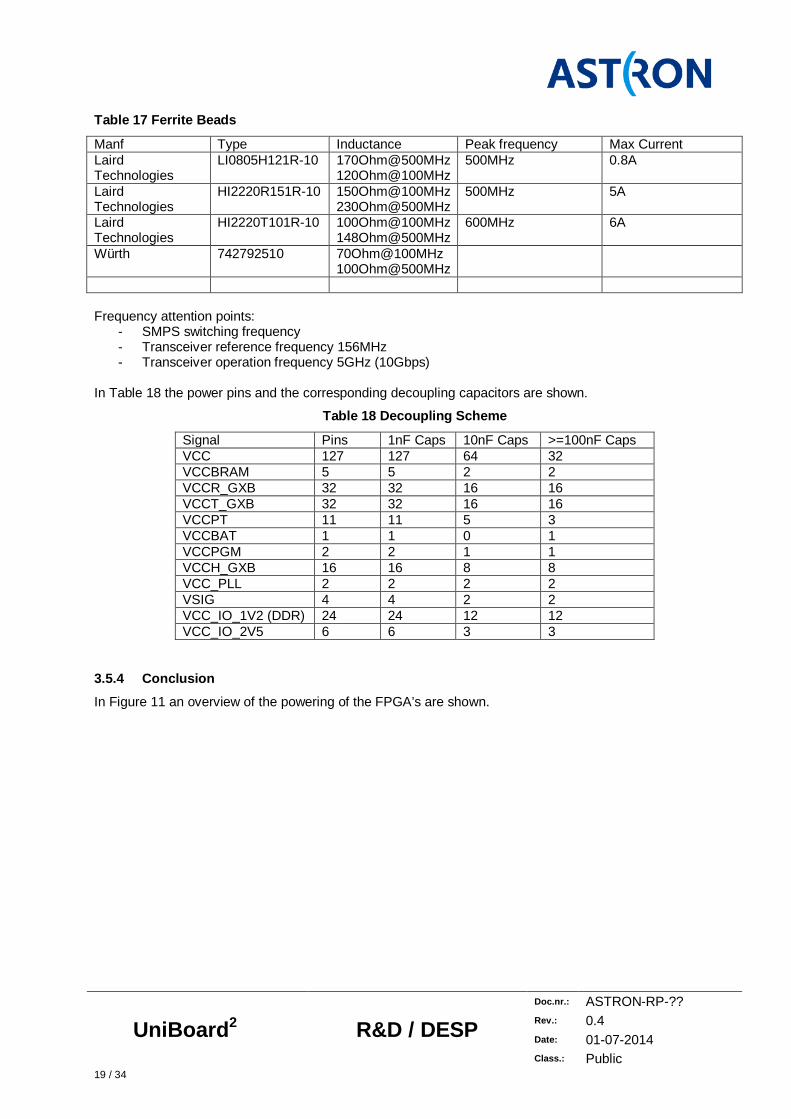
Table 17 Ferrite Beads
Manf Type Inductance Peak frequency Max Current Laird Technologies
LI0805H121R-10 170Ohm@500MHz 120Ohm@100MHz
500MHz 0.8A
Laird Technologies
HI2220R151R-10 150Ohm@100MHz 230Ohm@500MHz
500MHz 5A
Laird Technologies
HI2220T101R-10 100Ohm@100MHz 148Ohm@500MHz
600MHz 6A
Würth 742792510 70Ohm@100MHz 100Ohm@500MHz
Frequency attention points:
- SMPS switching frequency - Transceiver reference frequency 156MHz - Transceiver operation frequency 5GHz (10Gbps)
In Table 18 the power pins and the corresponding decoupling capacitors are shown.
Table 18 Decoupling Scheme
Signal Pins 1nF Caps 10nF Caps >=100nF Caps VCC 127 127 64 32 VCCBRAM 5 5 2 2 VCCR_GXB 32 32 16 16 VCCT_GXB 32 32 16 16 VCCPT 11 11 5 3 VCCBAT 1 1 0 1 VCCPGM 2 2 1 1 VCCH_GXB 16 16 8 8 VCC_PLL 2 2 2 2 VSIG 4 4 2 2 VCC_IO_1V2 (DDR) 24 24 12 12 VCC_IO_2V5 6 6 3 3
3.5.4 Conclusion In Figure 11 an overview of the powering of the FPGA’s are shown.

UniBoard2 R&D / DESP
Doc.nr.: ASTRON-RP-?? Rev.: 0.4 Date: 01-07-2014 Class.: Public
20 / 34
FPGA
VCCVCCP
BRM46412V->0.9V
0V9
VCCERAM
VCCR_GXB[L,R
BMR46112V->0.95V
0V95
BMR46112V->1.0V1V
VCC_BAT, VCCH_GXB
BMR46112V->1.8V
1V8
DDR41V8
ADM1186-2
EN
EN
EN
MAX17000A12V->1.2V
EN
2V5BMR461
12V->2.5VEN
IO
I2C
ADUM
VCCT_GXB[L,RBMR461
12V->1.0VEN
EN
1V
Con
nect
or
To micro-Processor
I2C
I2C
I2C
Figure 11 FPGA power scheme
For the adjustments of the power supplies firmware implementation is chosen. This is done because Altera has dedicated firmware IP to optimally adjust power levels to reduce power consumption. To reduce loss in the PCB, remote sensing of the power supplies will be used [15]. To prevent oscillation of the control loop an extra high frequency bypass capacitors will be placed between the sensor lines and the output of the DC/DC converter. For the SMBus (I2C) interface between the FPGA and the power modules a level translator is needed. In section 7.3 options for the level translators are shown.
3.6 FPGA attention points • Pinning must be done with migration to Stratix 10 in mind • Maximal power on FPGA pins 3V. • It must be possible to adjust the power levels • DDR pinning, check FPGA (Address in the middle with controller (total 3 banks for single interface)
3.7 Tools used for the design • Power distribution network simulator Altera
http://www.altera.com/technology/signal/board-design-guidelines/sgl-bdg-index.html • IO-Designer for pin assignments
3.8 ES limitations The major ES limitations are:
• For the configuration only the first 256Mb can be used. This means that: o compression is needed o Only one image in the flash (although normal mode can be used for the remaining parts of
the flash • JTAG limited to 7MHz

UniBoard2 R&D / DESP
Doc.nr.: ASTRON-RP-?? Rev.: 0.4 Date: 01-07-2014 Class.: Public
21 / 34
•
3.9 I2C Addresses In Table 19 the I2C interfaces for the FPGA are shown. The last FPGA (node3) has the power devices connected to the sens I2C interface.
Table 19 I2C addresses
Bus 7 bits I2C Address Function Chip Nodes MB_I2C 0x18 TEMP. DDR4_MB_I JEDEC TSE2004av 0,1,2,3 MB_I2C 0x19 TEMP. DDR4_MB_II JEDEC TSE2004av 0,1,2,3 SENS 0xA0h EEPROM CAT24C02 0,1,2,3 SENS 0x4Ch Temp. sensor TMP451 0,1,2,3 PMBus 0x01h Core supply BMR464 0,1,2,3 PMBus 0x0Dh VCC RAM BMR461 0,1,2,3 PMBus 0x0Eh Transceiver power supply BMR461 0,1,2,3 PMBus 0x0Fh Transceiver power supply BMR461 0,1,2,3 PMBus 0x10h Control power supply BMR461 0,1,2,3 PMBus 0x11h FPGA IO power supply BMR461 0,1,2,3 SENS 0x01h QSFP0 power supply BMR464 3 SENS 0x02h QSFP1 power supply BMR464 3 SENS 0x0Dh CLK power supply BMR461 3 SENS 0x0Eh 3V3 power supply BMR461 3 SENS 0x0Fh 1V2 power supply BMR461 3 SENS 0x2Bh PIM (power input module) PIM4328PD 3 SENS 0x2Ch DC/DC converter BMR456 3 SENS 0x29h Temp. Sensor Switch MAX1617A 3
4 DDR Next to every FPGA two DDR4 SODIMM will be placed. These DIMM’s will be placed in SODIMM sockets according JEDEC-SO-018A (October 2012) [5] standard. At the moment no vendor type number is known for the socket. As start the Micron MTA18ASF1G72HZ 8 GByte module [6] will be taken.
4.1 Glue Logic for DDR The serial control lines (SDA and SCL) will be connected to the FPGA. This interface can be used to readout the temperature and the SPD EEPROM.
4.2 Power for DDR The power requirements for the MTA18ASF1G are shown in Table 20.
Table 20 DDR4 power supplies
Signal Description Voltage Max. Current single module VDD 1.2V 2034mA (max in table) Vpp 2.5V 153mA (max in table) VrefCA Reference power 0.5*VDD VTT Termination power 0.5*VDD +/- 750mA VDDSPD Power for serial interface 2.2-3.6
From this table it can be seen that the peak current for two modules is more than 4A, a max sink/source for the VTT of 1.5A

UniBoard2 R&D / DESP
Doc.nr.: ASTRON-RP-?? Rev.: 0.4 Date: 01-07-2014 Class.: Public
22 / 34
Options for the power implementation are:
• MAX17000A (like is used on UniBoard1). Modification needed to let it run on 1.2V (lowest power is 1.0V). Max sink source VTT +/- 2A. FET’s capable of sufficient power. Special care for the layout needed to reduce power drop in the signals. 12V at the input of the DC/DC converter is not a problem.
• TPS51916, complete DDR power solution with 2A sink/source termination regulator. • TPS51100, 3A sink/source termination regulator
For UniBoard2 a single MAX17000A will be placed per FPGA powering two DDR4 modules.
4.3 General Remark The following attention points will be taken into account:
• Low pass filter VREF helps filter noise (wide trace, large spacing to neighbouring traces) • Good power bussing to reduce SSO • Check plane crossings (eliminate return path discontinuities (RPDs). • Place cap’s close to load (for sensitive powers on the top)
5 Backplane interface To make systems with multiple UniBoards, backplane connectors will be used on one side of the board. The maximal speed of the connector will be by design 25Gbps (In practice with the first board the speed will be up-to 10Gbps).
5.1 Power Connections UniBoard will receive its power through the backplane connector. The pins that are needed for the power are given in Table 21.
Table 21 Backplane connector power pin's.
Signal Description Number of contracts 48V Positive High side of the 48V input supply 1 48V Negative Low side of the 48V input supply 1 TOTAL 2
Although the number of pins is low, the power is with 15A relative high. Options for the connector are summarized in Table 22.
Table 22 Power connector options
Connector Manf Pins Pro Con 2mm HM Erni / TE 3 / Known on UniBoard Current limited to 15A
No signal pins Impact Molex / TE 4 15A per contact
Hold down option for screw mounting
No signal pin’s
Molex Part number are: Daughter card 78211-1001 Backplane 78212-1001 RAM 78348-1001. The connectors are shown in Figure 12.

UniBoard2 R&D / DESP
Doc.nr.: ASTRON-RP-?? Rev.: 0.4 Date: 01-07-2014 Class.: Public
23 / 34
Figure 12 Power connectors
5.2 Control Pins The control signals to interface to other (UniBoards) on the backplane are shown in Table 23.
Table 23 Control pins needed on the backplane.
Signal Description Number of contracts JTAG signals TDO, TDI, TMS, TCK 4 on/off Signal to switch UniBoard off 1 Sync Sync signal across boards on a
backplane 1
Clk Clock signal 1 pair PPS Pulse Per Second 1 pair Ethernet (optional) Ethernet control interface 2 pairs Total pins 14 pins
5.3 Signal Pins Each FPGA will have a set of connectors to the backplane. Although the pinning of these connectors will be as equal as possible for each FPGA, the board control signals might be distributed amount the signal connectors. In Table 24 an overview of the FPGA signals is given.
Table 24 Backplane connector power pin's.
Signal Description Number of contracts Link 0 First link for HMC / IO (25Gbps) 2x16 pairs=32 pairs Link0 CTRL I2C / lowspeed logic 4 signals Link 1 Second link for HMC / IO (10Gbps) 2x16 pairs=32 pairs Link1 CTRL I2C / lowspeed logic 4 signals Link 2 Third link for HMC / IO(10Gbps) 2x16 pairs=32 pairs Link1 CTRL I2C / lowspeed logic 4 signals Other SerDes for Mesh / IO 24 pairs=48 pairs Other CTRL Control for IO 4 signals Total 152 Pairs
304pins (excl. GND) Options for the connector are summarized in Table 25.

UniBoard2 R&D / DESP
Doc.nr.: ASTRON-RP-?? Rev.: 0.4 Date: 01-07-2014 Class.: Public
24 / 34
Table 25 Signal connector options
Connector Manf Pairs Pro Con ERmetZD Erni 40 (4x10) 20Gbps Nof pairs limited
10DP/cm ERmetZD HD Erni 84 (6x14) 25 Gbps
GND connection RAM unknown
Impact (2132723-1)
TE / Molex 72 / Ground 20-25Gbps 16DP/cm Othrogonal / Coplanar (RAM)
TE Impel Molex 25-40Gbps
16DP/cm 92 Ohm
XCede Orthogonal Amphenol TCS 36 (4x6 / 6x6) Orthogonal 25Gbps 85/100Ω
Given the high density of the connector back drilling is an option to maintain the signal integrity. This will be discussed with the PCB manufacturer. For UniBoard2 the Impact (RAM) connector will be used. Backplane connector priority is:
1. RAM (right angle module with HMC devices) 2. Standard backplane 3. Orthogonal backplane
Table 26 Impact part numbers
Pairs MANF Configuration Daughter Card Backplane RAM Dimension 60 TE 10x 6 pairs 2007741-1 2007884-1 Not available 80 TE 16x 5 pairs 2110124-1 2007868-1 Not available 96 TE 16x 6 pairs 2007747-1 2007900-1 Not available 60 MOLEX 10x 6 pairs 76150-1010 76145-1104 76560-1107 21.7mm 80 MOLEX 16x 5 pairs 76060-1016 76055-1604 Not available 33.1mm 96 MOLEX 16x 6 pairs 76150-1016 76145-1604 76560-1607 33.1mm 60 MOLEX 10x6 pairs 76290-1010 (OR) 76285-1128 (OR) Not available 22.9mm 72 MOLEX 6x12 pairs 76290-1012 (OR) 76285-1204 (OR) Not available 27.0mm
The spacing between columns is different between orthogonal and standard connectors (10 columns distance between both sides for orthogonal 18.1mm and standard 17.1mm) With ~140 pairs per FPGA two 96 pair Molex connectors will be used (with TE as alternative). One connector (in the middle) might be equipped with a guide pin.
Figure 13 Picture of backplane connectors

UniBoard2 R&D / DESP
Doc.nr.: ASTRON-RP-?? Rev.: 0.4 Date: 01-07-2014 Class.: Public
25 / 34
For the connectors 80mm (incl. Alignment) spacing is available. A 10 column connector is 22mm a 16 column connector 33mm. This means that two 16 column connectors can be placed on the board.
6 Control The control for UniBoard2 is split in two parts, the control on the FPGA and the board control. Both control interfaces are implemented with Ethernet interfaces, and onboard switch is used to distribute the Ethernet to all parts. In Figure 14 in overview of the control is given.
FPGA 0
Ethernet Switch
RJ45
RJ45
RJ45
RJ45
FPGA 3
Board Sensors (supply voltages)
4x
8x SGMII
I2C
PHY
Optical Interface
Optical Interface
Optical Interface
Optical Interface
Temperature Sensors Power SupplyTemperature
Sensors Power Supply
ETH
I2C PMBUSI2CPMBUS
Figure 14 UniBoard control
6.1 Ethernet Switch For the switch the same switch as is used for UniBoard1 (Vitesse VSC7389 [7]) will be used. This switch has 8 SGMII interfaces (each interface consist of two pairs, one for transmit and one for receive) for connecting the FPGAs, and 8 integrated tri-speed copper transceivers from which four will be connected to the front side of the board. The VSC7389 has an EEPROM for controlling the switch. Via the on-chip 8051 V-core CPU Web-based and SNMP management is made possible.
6.1.1 Other options Other options for the switch are shown in Table 27.
Table 27 Switch options
Type Manufacturer Spec Remark BCM56640 Broadcom 24x10Gbps
4x Multilayer Gagabit Broadcom does not support small companies / institutes to route their own boards.
VSC7389 Vitesse 24x 1Gbps 4x 10Gbps
MT51164A2 Mellanox 64 Port 10GbE CPU with PCIe needed to set switch
6.1.2 RJ45 Ports
On UniBoard2 six RJ45 ports will be placed. In this case 4 ports can be used for fast data offload and the other two ports for control. When space is limited (both along the board edge as in height) a 2x2 might be

UniBoard2 R&D / DESP
Doc.nr.: ASTRON-RP-?? Rev.: 0.4 Date: 01-07-2014 Class.: Public
26 / 34
placed on the board and two ports on the extension board. For the connector a through hole connector will be used, this will reduce the risk of breaking of a connector. By using an stacked version board space can be saved. Ideally a 3x2 would be used but 3 times a 1x2 could also be used. By integrating the magnetic in the connector a further board space reduction can be achieved. Connector options shown in Table 28.
Table 28 RJ45 Control connector selection
The Bel fuse / Steward will be used on UniBoard2.
7 Power Entry The general power tree of UniBoard2 is shown in Figure 15.
Memory Power Supply Memory
-48V
12V intermediate power
POL12V to 0.9V
POL12V to 2.5V
FPGA
Optical Interface Power Supply
Optical Interfaces
Circuit Protection
Intermediate Bus Converter
Power Monitoring
Figure 15 UniBoard Power tree
At the input the power is projected (short circuit) and fed to a Bus Converter to convert the 48V isolated input to 12V. The 12V is distributed across the board. Near every FPGA a point of load converted is used to make the local power supplies. The powers for the FPGA and the DDR are discussed in the sections 3.5 and 4.2 respectively.
7.1 Power consumption An estimation of the power consumption of the different parts of UniBoard2 is shown in Table 29.
Manf. Part number Configuration Magnetics included Remark Würth 7499151120 1x2 Yes TE 1840649-4 2x2 No Low profile Steward/Bel C850-2C3R-54 2x3 Yes Molex - Erni -

UniBoard2 R&D / DESP
Doc.nr.: ASTRON-RP-?? Rev.: 0.4 Date: 01-07-2014 Class.: Public
27 / 34
Table 29 UniBoard Power estimation
Power Power single item
Power total efficiency Max. estimated Power
Optics 3.5W 84W 0.9*0.9=0.81 100 FPGA 40W 160W 0.9*0.9=0.81 200 Memory 5W 40W 0.8*0.9=0.72 60 Ethernet switch 7W 7W 0.9*0.9=0.81 10 Others 30 Total 400W
Given a 48V power supply, the current at the input is approximately 9A, and the current at the output of the DC/DC converter 35A
7.2 Circuit protection At the input of UniBoard circuit protection will be placed to prevent damage by shot circuit, power supply glitches etc. To prevent damage by spikes on the power inlet TVR diodes and sufficient large capacitors will be placed on the 48V power inlet.
Table 30 Hot swap controllers
Type Manufacturer Functions Remark LTC4260 Linear Technology Incl. sensors Used on UniBoard1 LTC4260 Linear Technology Incl. sensors Neg power LM5064 Ti Sensors SMBus Neg. power ADM1075 Analog Devices
Instead of a hot swap controller a chip fuses can be used as well. An example of a chip fuse is the Littelfuse 451 NANO2® series. In this series a very fast-acting subminiature fuses up to 15A can be used. Instead of building a discrete input section on UniBoard an Ericsson PIM module (Power Interface Module) can be placed as well. On this module all input functions like, inrush protection, transient suppression, monitoring and control are implemented. On UniBoard2 a PIM module will be placed. When space is limited the old hot swap controller will be placed with a fuse as by pass. By using the old hot swap firmware can be reused. With this controller power consumption of the UniBoard can be measured.
7.3 I2C Isolator / Level translator To connect the hot swap controller to e.g. and FPGA an isolator between isolated input to the ground referenced board domain is needed. In Table 31 examples of isolators are shown.
Table 31 I2C Isolators
Type Manufacturer Power supplies Logic Remark ADUM2402 Analog Devices Used on UniBoard ADUM1251 Analog Devices 3.0-5.5V I2C LTM2883-I Linear Technology ±12.5V and 5V I2C LTC4313-3 Linear Technology Only level translator ISO7231 Ti 3.15-5.5 Tripple Isolater
On UniBoard2 we will use the ADUM1251. The difference between the input and output at logic low is 50mV, this should ensure that there is no possibility of latching up the bus.

UniBoard2 R&D / DESP
Doc.nr.: ASTRON-RP-?? Rev.: 0.4 Date: 01-07-2014 Class.: Public
28 / 34
7.4 Isolated DC/DC converter To convert the isolated 48V to the local 12V a standard size converter is used. In Table 32 an overview of the different options are shown.
Table 32 Isolated DC/DC converters
Part Number QBVS050A0B BMR456 BMR453 IB048Q120T60 QME48T35120 Manf. GE Ericsson Ericsson Vicor Power One Size Quarter Brick Quarter Brick Quarter Brick Quarter Brick QuarterBrick Output Power 600W 396 / 700W 468W 720W 420W Control Not available PMBus PMBus Not available Not available Efficiency @25A 96% 96% 96% 97.5% 96% Remark 4:1 IBC Price indication €101@15st €74.66 @ 1 €118.7 @ 1 - -
7.5 Remarks For the design of the distribution network, including decoupling, the PDN simulation tool of Altera, as described in [13] will be used. Besides this tool Hyperlynx will be used to analyse the power distribution network as well.
7.6 ON/OFF For the FPGA up and down sequencing is needed. This means that the power cannot be switch off external, the boards needs shutdown first. For this a push-button will be mounted on the board. This button will be instead of the reset button. In Figure 16 and examples of the button is shown (C&K ELUM-EE-SA-Q).
Figure 16 ON/OFF latching pushbutton
The reset line will be fed to the backplane. In this way or a shut down can be send to a back module or a central board can shutdown the UniBoard2.
8 Clock and Sync On UniBoard a system clock and the PPS will be distributed. To enable high fan-out of the PPS signal, the PPS will be connected on a clock input pin as well [17]. The lines, both clock and PPS will be tuned to equal length to all FPGA up-to <0.1ns (10mm/400mill). Both clock and PPS will have a differential distributed. According [17] LVPECL or LDVS can be used, where the clock termination is done internal. When a LVDS clock is used the signal will be DC-coupled, with LVPECL an AC coupled signal will be used. In Table 33 an overview of the levels is shown.
Table 33 LVDS and LVPECL levels
LVDS [V]
LVPECL LVPECL @ 2.5V
Low 0.900 (min) Vcc-1.99 (min) 0.51 High 1.600 (max) Vcc-0.76 (max) 1.74 Differential 0.450 (max) 1.23 (max) Offset 1.1125-1.375 1.125 (typ.)
In Table 34 an overview of clock/pps buffers is shown:

UniBoard2 R&D / DESP
Doc.nr.: ASTRON-RP-?? Rev.: 0.4 Date: 01-07-2014 Class.: Public
29 / 34
Table 34 Clock fanout buffers
Part Number Manufacturer Fanout Output Level Input Level Power Remark NB6L14S On
Semiconductor 1:4 LVDS Any Level 2V5
ADCLK946 Analog Devices 1:6 LVPECL ADN4670 Analog Devices 2:10 LVDS CY2DP1504 Cypress 2:4 LVPECL Any 2V5/3V3 Dual input CY2DL1504 Cypress 2:4 LVDS Any 2V5/3V3 Dual input PL138-48 Micrel 2:4 LVPECL SY89847U Micrel 2:5 LVDS any Dual input ICS8543 IDT 2:4 LVDS 3V3 Altera Kit
For the CY2DL1504 is chosen. By using this buffer a system clock crystal can be placed on the board simplifying single board applications. All clocks will be LVDS. The CY2DL1504 has 0.11ps additive RMS phase jitter, less then 30ps output-to-output skew and less then 150ps device-to-device skew. For the Transceivers the same clock structure will be used. Two crystals will be mounted on the board one crystal for the front transceivers and one for the backside transceivers.
9 Test strategy In Table 35 the test strategy is described.
Table 35 Overview Test strategy
Item Test equipment Remark Slow speed interconnections - Boundary scan
-
Transceiver links - Firmware - Boundary scan
IEEE 1149.6 is now supported by Arria10 which enables boundary scan of the transceivers.
DDR interface - Boundary scan in combination with dummy module
9.1.1 Boundary scan
The board will be equipped with a boundary scan interface. Via this interface access will be provided to all boundary scanable devices. This will enable testing the board before the FPGAs are programmed. Comparable solutions as used for UniBoard will be used.
Table 36 JTAG Signal levels
JTAG interface Level TAPs FPGA 1.8V 2 (2 FPGA’s per tap) Ethernet Switch 2.5V 1
Altera supports both the IEEE 1149.1 and the 1149.6 JTAG standards. The IEEE 1149.6 specification specifies testing of high-speed differential interconnections. For testing loopback modules / boards will be made to test the DDR interfaces and the SerDes channels. An overview of the Boundary scan setup is shown in Figure 17.

UniBoard2 R&D / DESP
Doc.nr.: ASTRON-RP-?? Rev.: 0.4 Date: 01-07-2014 Class.: Public
30 / 34
FPGA 2
JTAG Bridge
FPGA 3
FPGA 0
FPGA 1Switch
TAP1TAP3TAP5
Backplane
Altera USB-Blaster
Mem
ory
Loop
bac
kS
erD
esLo
op b
ack
TAP2TAP4
Con
nect
or
Figure 17 Boundary scan overview
For the scan bridge the Lattice BSCAN2 IP will be used. This IP can only be used on Lattice FPGA/CPLD’s. In Table 37 an overview of the devices is shown.
Table 37 Lattice Semiconductor FPGA/CPLD options
Device Type / Family Package Remark LCMXO640-5T100C CPLD MachXO 17x17mm 100TQFP Used on UniBoard LCMXO2-640 E-1 TG100 CPLD MachXO2 17x17mm 100TQFP LCMXO2-640 E-1 MG132 CPLD MachXO2 8x8mm Fineline BGA LFXP2-8E-5 FTN256 FPGA XP2-8 17x17mm 256pins ftBGA LFXP2-8E-5 TN144 FPGA XP2-8 20x20mm 144 TQFP LFXP2-17E-5 QN208 FPGA XP2-17E 208mm PQFP Used on PAC For UniBoard2 the LCMXO2-640HC in a 100TQFP package will be used.
10 PCB As a start the same layer stack will be used as with UniBoard1, see Figure 18.
1
Prepreg Core
2345678
109
111213141516
W WS C
H Tεr
εr = 3.5Width, W = 0.1mm (4 mill)Spacing S = 0.15mm (6 mill)Height H = 2x0.146mmCopper tickness T = 0.5 oz. = 18umClearence C = 0.5mm (1.5xH)Total: 0.9mm
Total single trace
Figure 18 Layer stack

UniBoard2 R&D / DESP
Doc.nr.: ASTRON-RP-?? Rev.: 0.4 Date: 01-07-2014 Class.: Public
31 / 34
Instead of standard FR4 used for UniBoard, UniBoard2 will use Panasonic Megtron-6 Df 0.002 to increase the speed to 25Gbps. Pro’s Megtron 6
- 10x lower Tan(delta) (0.002) 10dB less loss - Smaller Er means bigger traces means less loss - Smaller Er means more layers in 2.4mm
Con’s Megtron6 - 5 times more expensive than standard FR4
For the fast traces to the QSFP+-cages the layer 12 and 3 will be used as much as possible (there the via length is limited). The spacing between the traces will be such that the traces are loosely coupled; this makes it easier to maintain impedance.
Table 38 Estimates layer according Altera
By using a more complex via scheme it is expected that a PCB with less layer can be made.
10.1.1 Remarks
From the Altera application notes [10],[11] and [12] the following remarks are applicable. Remarks concerning the layer stack up:
- Expected number of signal layer is column depth to power divided by 2, 1917pins 44 columns Routing remarks
- Remove non functional pad’s of via (drawback more stress on via’s) - Increase antipad. - Add ground via (for >5GHz) - Tune length of via (blind via / back drilling)
Before the layout of UniBoard2 will start, a discussion with the PCB supplier will take place. In this discussion the material selection and the technologies used (microvia’s) will be discussed. By using blind, buried and micro via’s the number of layer might be reduce to an acceptable number.
11 Green To make steps towards green processing the following steps will be taken:
• RoSH compliant • Reduce the use of tantalum components • Use efficient power supplies (this reduces heat. Less power needed for cooling) • Enable shutdown for power supplies (if DDR is not used, switch off the power) • Liquid cooling • Remove functionality what is not really needed (this also reduce debug time)

UniBoard2 R&D / DESP
Doc.nr.: ASTRON-RP-?? Rev.: 0.4 Date: 01-07-2014 Class.: Public
32 / 34
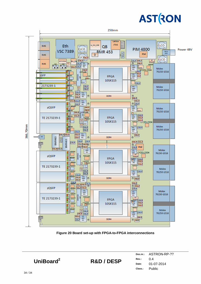
12 Board layout The board is build round four equal nodes with in the middle the power. The height of the board is the standard 9U (366mm). The width will be standard but adjusted to the needed space. In Figure 19 an overview of the board is shown.

UniBoard2 R&D / DESP
Doc.nr.: ASTRON-RP-?? Rev.: 0.4 Date: 01-07-2014 Class.: Public
33 / 34
Figure 19 Overview of UniBoard2
UniBoard2 R&D / DESP
Doc.nr.: ASTRON-RP-?? Rev.: 0.4 Date: 01-07-2014 Class.: Public
34 / 34
Figure 20 Board set-up with FPGA-to-FPGA interconnections