Under the Hood of Flyback SMPS Designs
39
Under the Hood of Flyback SMPS Designs Bing Lu Topic 1
Transcript of Under the Hood of Flyback SMPS Designs
Under the Hood of Flyback SMPS Designs
Bing Lu
Topic 1

Texas Instruments—2010 Power Supply Design Seminar 1-2
Agenda
1. Basics of Flyback Topology
2. Impact of Transformer Design on Power Supply Performance
3. Power Supply Current Limiting
4. Summary
Texas Instruments—2010 Power Supply Design Seminar 1-3
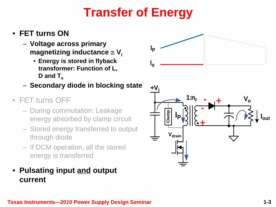
Transfer of Energy• FET turns ON
– Voltage across primary magnetizing inductance ≅ Vi
• Energy is stored in flyback transformer: Function of L, D and Ts
– Secondary diode in blocking state
• FET turns OFF– During commutation: Leakage
energy absorbed by clamp circuit– Stored energy transferred to output
through diode– If DCM operation, all the stored
energy is transferred
• Pulsating input and output current
1:n2
+Vi
Vo
Cla
mp
Vdrain
Iout+-
+-IP
Io
IP
Texas Instruments—2010 Power Supply Design Seminar 1-4
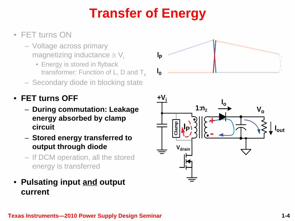
Transfer of Energy• FET turns ON
– Voltage across primary magnetizing inductance ≅ Vi
• Energy is stored in flyback transformer: Function of L, D and Ts
– Secondary diode in blocking state
• FET turns OFF– During commutation: Leakage
energy absorbed by clamp circuit
– Stored energy transferred to output through diode
– If DCM operation, all the stored energy is transferred
• Pulsating input and output current
1:n2
+Vi
Vo
Cla
mp
Vdrain
Iout+-IP
Io
IP
Io

Texas Instruments—2010 Power Supply Design Seminar 1-5
Transfer of Energy• FET turns ON
– Voltage across primary magnetizing inductance ≅ Vi
• Energy is stored in flyback transformer: Function of L, D and Ts
– Secondary diode in blocking state
• FET turns OFF– During commutation: Leakage
energy absorbed by clamp circuit– Stored energy transferred to
output through diode– If DCM operation, all the stored
energy is transferred
• Pulsating input and output current
1:n2
+Vi
Vo
Cla
mp
Vdrain
Iout+-
Io
IP
Io

Texas Instruments—2010 Power Supply Design Seminar 1-6
Transfer of Energy• FET turns ON
– Voltage across primary magnetizing inductance ≅ Vi
• Energy is stored in flyback transformer: Function of L, D and Ts
– Secondary diode in blocking state
• FET turns OFF– During commutation: Leakage energy
absorbed by clamp circuit– Stored energy transferred to output
through diode– If DCM operation, all the stored
energy is transferred
• Pulsating input and output current
1:n2
+Vi
Vo
Cla
mp
Vdrain
Iout

Texas Instruments—2010 Power Supply Design Seminar 1-7
CCM versus DCM• Continuous conduction mode (CCM)
– Small ripple and rms current– Lower MOSFET conduction and
turn-off loss– Lower core loss– Lower capacitors loss– Can have better “full load” efficiency– Smaller EMI and output filters
• Discontinuous conduction mode (DCM)– No diode reverse recovery loss– Lower inductance value
• May result in a smaller transformer– Better “no load” efficiency– First-order system
• Inherently stable– No RHPZ problem– Slope compensation not needed
in CMC
PrimaryMOSFET
Time (t)
IpkIpkmin
PrimaryCurrent
T
m2SSecondaryCurrent
IoIo_avg
IP
Vdrain
ΔIL
ΔILS
D x Ts(1 – D) x TsVo + Vin2
Time (t)
Vdrain
IP
Ts
D × TsVi
Ipk
Io_avg
(1 – D) × Ts
Io
PrimaryMOSFET
PrimaryCurrent
SecondaryCurrent
IdlePeriod
Vo + Vin2
Texas Instruments—2010 Power Supply Design Seminar 1-8
1:n2
+Vi
Vo
Clam
p
Vdrain
Iout+-
+-IP
1:n2
+Vi
Vo
Clam
pVdrain
Iout+-
Io
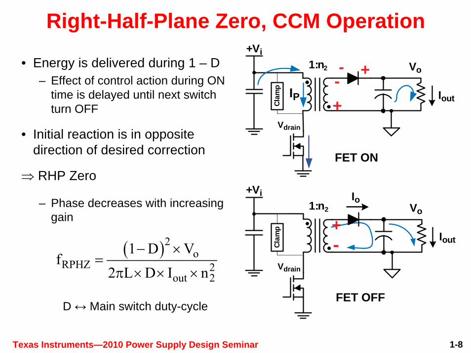
Right-Half-Plane Zero, CCM Operation
• Energy is delivered during 1 – D– Effect of control action during ON
time is delayed until next switch turn OFF
• Initial reaction is in opposite direction of desired correction
⇒ RHP Zero
– Phase decreases with increasing gain
( )2o
RPHZ 2out 2
1 D Vf
2 L D I n− ×
=π × × ×
FET ON
FET OFFD ↔ Main switch duty-cycle
Texas Instruments—2010 Power Supply Design Seminar 1-9
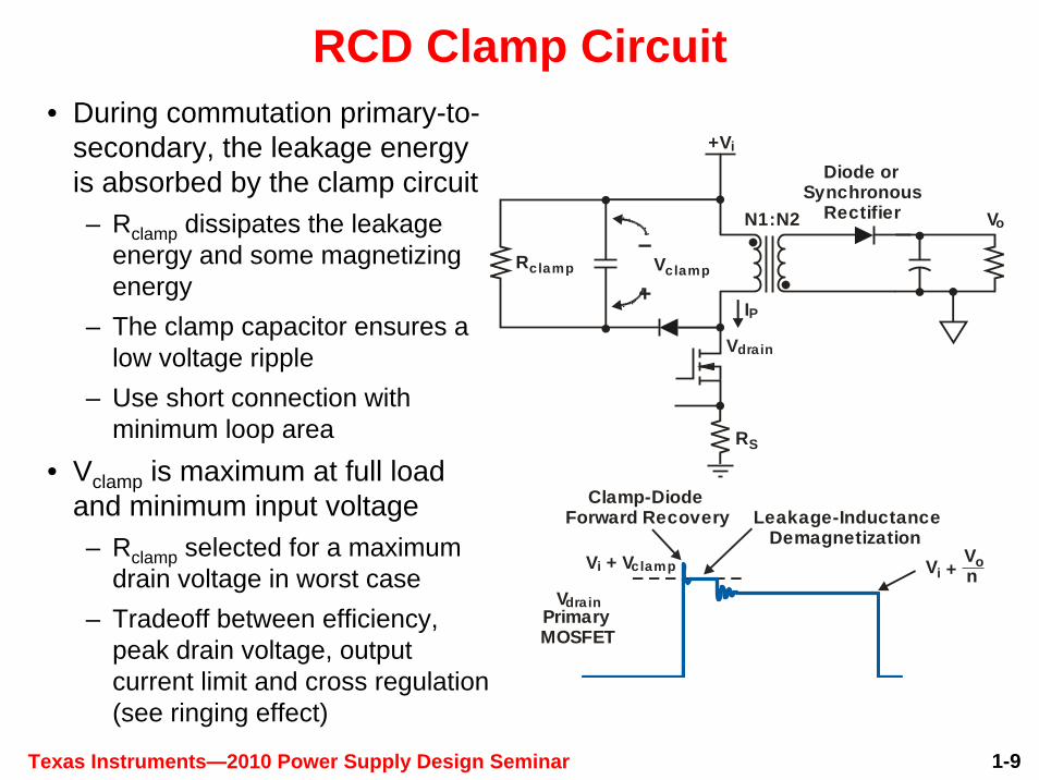
RCD Clamp Circuit• During commutation primary-to-
secondary, the leakage energy is absorbed by the clamp circuit– Rclamp dissipates the leakage
energy and some magnetizing energy
– The clamp capacitor ensures a low voltage ripple
– Use short connection with minimum loop area
• Vclamp is maximum at full load and minimum input voltage– Rclamp selected for a maximum
drain voltage in worst case– Tradeoff between efficiency,
peak drain voltage, output current limit and cross regulation (see ringing effect)
Rclamp Vclamp+
–
+Vi
Diode orSynchronous
Rectifier Vo
IP
Vdrain
RS
N1:N2
VdrainPrimaryMOSFET
V + Vi clamp
Clamp-DiodeForward Recovery Leakage-Inductance
DemagnetizationV
+ V no
i

Texas Instruments—2010 Power Supply Design Seminar 1-10
Agenda
1. Basics of Flyback Topology
2. Impact of Transformer Design on Power Supply Performance
3. Power Supply Current Limiting
4. Summary
Texas Instruments—2010 Power Supply Design Seminar 1-11
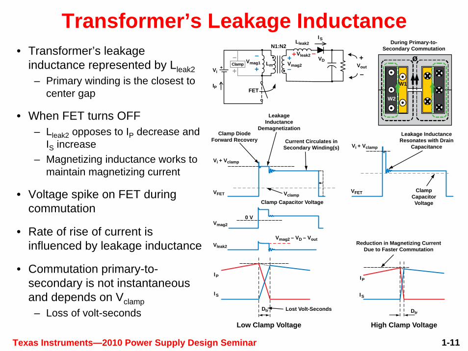
Transformer’s Leakage Inductance• Transformer’s leakage
inductance represented by Lleak2– Primary winding is the closest to
center gap
• When FET turns OFF– Lleak2 opposes to IP decrease and
IS increase– Magnetizing inductance works to
maintain magnetizing current
• Voltage spike on FET during commutation
• Rate of rise of current is influenced by leakage inductance
• Commutation primary-to-secondary is not instantaneous and depends on Vclamp– Loss of volt-seconds
Lleak2
Clamp+
ø
0 V
Vi
IP
+
+–+
+–
–
–Vmag1 Vmag2Lm
VDVleak2
FET
Vout
+
–
N1:N2IS
W1
W2
During Primary-to-Secondary Commutation
Vi + Vclamp
Vmag2 – VD – Vout
VclampVFET
Vmag2
Vleak2
IP
IS
Lost Volt-Seconds
Low Clamp Voltage High Clamp Voltage
Dtr
Clamp Capacitor Voltage
Clamp DiodeForward Recovery
LeakageInductance
Demagnetization
Current Circulates inSecondary Winding(s) Vi + Vclamp
VFET
Leakage InductanceResonates with Drain
Capacitance
ClampCapacitorVoltage
Dtr
IP
IS
Reduction in Magnetizing CurrentDue to Faster Commutation

Texas Instruments—2010 Power Supply Design Seminar 1-12
Effects of Leakage Inductance
• Clamp circuits and snubbers needed for primary FET and secondary rectifier(s)
• Lower power-supply efficiency
• Impact on gate-drive strategy if synchronous rectifier is used
• Higher duty cycle and magnetizing current than expected
• Higher H-field radiated emission
• High impact on cross-regulation

Texas Instruments—2010 Power Supply Design Seminar 1-13
How Leakage Can Be Minimized• Leakage inductance is a function of winding geometry, number of turns
and separation between primary and secondary– Minimize the separation between the primary and main secondary
winding(s) – Interleave the primary and main secondary– Select a core with a long and narrow window
• Leakage inductance is not lowered with a high permeability core
• Having the winding tightly coupled to the core will not reduce it
Option 1 Option 2
W2 W1
L L
W1 W1
W1 W2
W2 W2
W2 W2
W1 W2
W1 W1
W2 W1
Texas Instruments—2010 Power Supply Design Seminar 1-14
Cross-Regulation – Overview
• Multiple-output flyback topology is popular because of its simplicity and low cost
• If the coupling is perfect, the turns ratio directly defines output voltages
• In the real world, “perfect” coupling is not possible
• This often results in poor cross-regulation
Texas Instruments—2010 Power Supply Design Seminar 1-15
Cross-Regulation Physical Model
• Transformer windings cannot all be equally well coupled to the gap because of physical separation between them
• Magnetic energy stored between the windings represented as leakage inductances
• Model not applicable to any transformer geometry
• Can become complex if interleaving is used, or if multiple secondary windings are wound simultaneously (multifilar)
• Not accurate in situation of lightly loaded secondary outputs
• Good tool to understand how the common flyback transformer geometries work

Texas Instruments—2010 Power Supply Design Seminar 1-16
Cross-Regulation Physical Model
• This circuit is only applicable to the transformer windings stackup shown
• Each leakage inductance considered is between two consecutive secondaries
• Also called “Ladder model”
+
–
lp Lleak12 Lleak23 Lleak34
++
+
+–
–
+–
+–
V2
Basic Flyback Circuit Transformer Construction
Transformer Physical Model
Clamp
Vi
LmVmag1Vi
V2
FET
FET
N1:N2
lp
lW4
lW3
lW2
W1
Prim
ary
W2
W3
W4
Clamp
N4 V4
N3 V3
N1:N2
N2:N3 N2:N4
+
–
+
–
+
–
I2I3
IW3IW4
V3 V4
I4

Texas Instruments—2010 Power Supply Design Seminar 1-17
Flux Lines during CommutationEach Secondary Winding with Nominal Load
• φm decreases during commutation
• dφ/dt (decreasing) in each secondary winding is limited by its output voltage
– Increasing current induced in W2 to W4 to maintain φm in the gap
• Leakage between W2 and W1– W1’s voltage limited by clamp
• W1 closest to gap– Vclamp limits dφm/dt in the gap during
commutation
• W2 is next to W1– W2 limits the dφ/dt seen by W3 and W4– W3 and W4 output voltage lower than
without leakage
• Current commutates progressively from near to remote secondary windings
mde Ndtφ
= − ×
φm
W1 W3 W4
W2
During Primary-to-Secondary CommutationCurrent in All Windings
L
I4
I3
I2lp
Secondary Currents DuringCommutation Based on Physical Model

Texas Instruments—2010 Power Supply Design Seminar 1-18
Ringing Effect• High dV/dt when main switch turns off if main output is heavily loaded
• Transformer leakage inductance and parasitic capacity ⇒ auxiliary secondary voltage tends to “ring”
• If auxiliary output fully loaded ⇒ this ringing is clamped
• If lightly loaded ⇒ voltage overshoot with peak detector effect
• Much higher (sometimes > 2 x nominal value!) auxiliary output voltage at light load – Primary clamp voltage has high impact on result
• Most existing transformer models fail to predict this
• This effect can be mitigated (but not eliminated)– Minimize leakage inductance between secondary windings– Locate the highest power secondary(ies) closest to the primary
• Other solutions include a post-regulator, series resistor or minimum load
Texas Instruments—2010 Power Supply Design Seminar 1-19
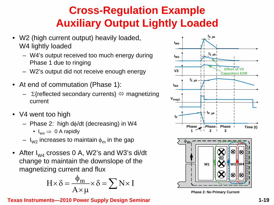
Cross-Regulation ExampleAuxiliary Output Lightly Loaded
• W2 (high current output) heavily loaded, W4 lightly loaded
– W4’s output received too much energy during Phase 1 due to ringing
– W2’s output did not receive enough energy
• At end of commutation (Phase 1): – Σ{reflected secondary currents} magnetizing
current
• V4 went too high– Phase 2: high dφ/dt (decreasing) in W4
• IW4 ⇒ 0 A rapidly– IW2 increases to maintain φm in the gap
• After IW4 crosses 0 A, W2’s and W3’s di/dt change to maintain the downslope of the magnetizing current and flux
mH N IAφ
×δ = ×δ = ××μ ∑
W1 W3 W4
W2
Phase 2: No Primary Current
Effect of V3Capacitors ESR
IW4
Time (t)
I4_pk
I3_pk
I2_pk
IP_pk
Phase1
Phase2
Phase3
IW3
IW2
IP
Vmag1
V3
φm
Texas Instruments—2010 Power Supply Design Seminar 1-20
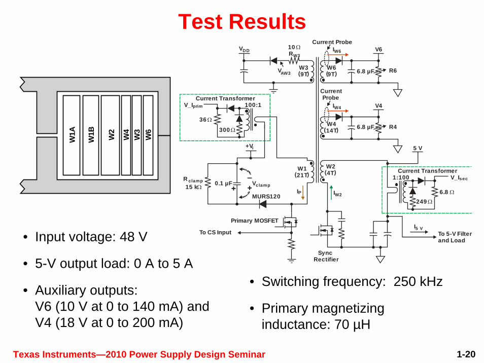
Test Results
• Input voltage: 48 V
• 5-V output load: 0 A to 5 A
• Auxiliary outputs: V6 (10 V at 0 to 140 mA) and V4 (18 V at 0 to 200 mA)
W3
W1A
W1B W2
W4
W6
V_Iprim 100:1Current Transformer
+Vi
6.8 µF
6.8 µF
W6(9T)
W4(14T)
W2(4T)W1
(21T)
W3(9T)
10 R
ΩW3
I W6
I W4
I W2I P
To 5-V Filterand Load
Primary MOSFET
SyncRectifier
Current Probe
CurrentProbe
MURS120
0.1 µF
To CS Input
R15 k
clampΩ
V6
V4
VDD
R6
R4
Vclamp
36 Ω
300 Ω
V_Isec1:100Current Transformer
6.8 Ω
I5 V
5 V
249 Ω
VAW3
• Switching frequency: 250 kHz
• Primary magnetizing inductance: 70 µH
Texas Instruments—2010 Power Supply Design Seminar 1-21
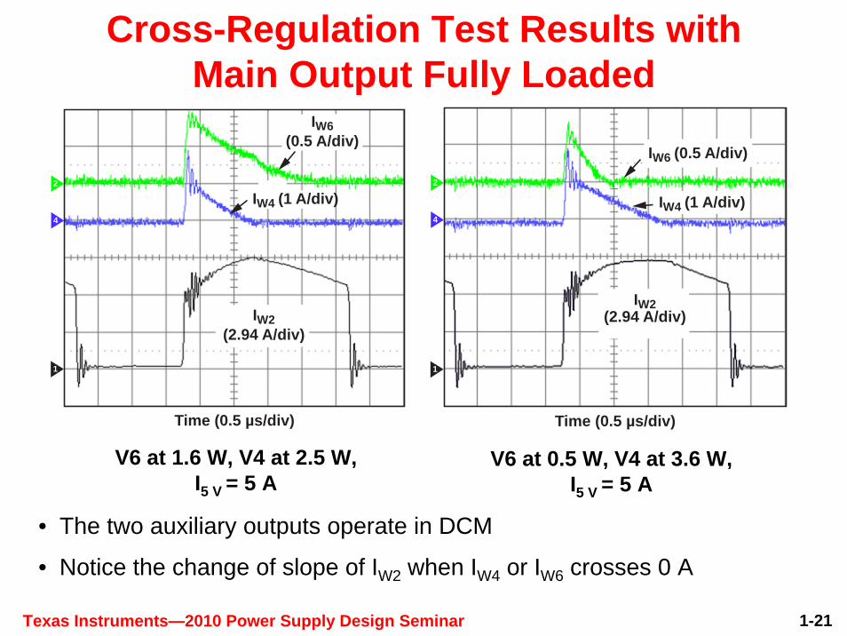
Cross-Regulation Test Results with Main Output Fully Loaded
V6 at 1.6 W, V4 at 2.5 W, I5 V = 5 A
4
2
1
IW6(0.5 A/div)
IW2(2.94 A/div)
IW4 (1 A/div)
Time (0.5 µs/div)
4
2
1
IW6 (0.5 A/div)
IW2(2.94 A/div)
IW4 (1 A/div)
Time (0.5 µs/div)
• The two auxiliary outputs operate in DCM
• Notice the change of slope of IW2 when IW4 or IW6 crosses 0 A
V6 at 0.5 W, V4 at 3.6 W, I5 V = 5 A
Texas Instruments—2010 Power Supply Design Seminar 1-22
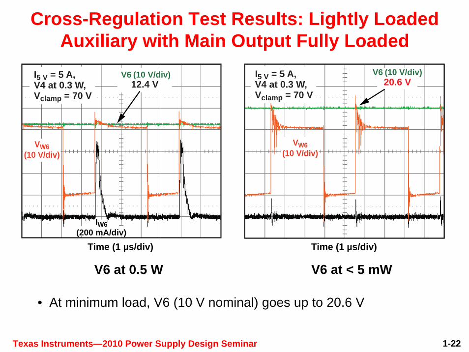
Cross-Regulation Test Results: Lightly Loaded Auxiliary with Main Output Fully Loaded
• At minimum load, V6 (10 V nominal) goes up to 20.6 V
V6 at 0.5 W V6 at < 5 mW
Time (1 µs/div)Time (1 µs/div)
12.4 VV6 (10 V/div)
VW6(10 V/div)
IW6(200 mA/div)
I5 V = 5 A,V4 at 0.3 W,Vclamp = 70 V
20.6 VI5 V = 5 A,V4 at 0.3 W,Vclamp = 70 V
VW6(10 V/div)
V6 (10 V/div)

Texas Instruments—2010 Power Supply Design Seminar 1-23
Cross-Regulation Test Results with Main Output Fully Loaded : Impact of Clamp Voltage
• RCD resistor has been increased for higher Vclamp: 70 V ⇒ 83 V
⇒V6 increased significantly in both cases
V6 at 0.5 W V6 at < 5 mWTime (1 µs/div)Time (1 µs/div)
26 V14.4 VV6 (10 V/div)
VW6(10 V/div)
IW6(200 mA/div)
I5 V = 5 A,V4 at 0.3 W,Vclamp = 83 V
VW6(10 V/div)
V6 (10 V/div)I5 V = 5 A,V4 at 0.3 W,
Vclamp = 83 V

Texas Instruments—2010 Power Supply Design Seminar 1-24
Overload Test at Auxiliary Output: Impact of Leakage
• There was no hiccup mode even at more than 3 A!
• The overloaded winding is unable to take all the energy because of leakage, W3 having in fact a better coupling to primary than W6– Enough energy
delivered by W3 to VDDto maintain switching
4
2
3
Time (0.5 µs/div)
IW4 (1 A/div)
VAW3 (20 V/div)
IW6 (2 A/div) 6.2-A Peak
I5 V = 0 A,V4 at 2.5 W,R6 = 1 Ω
Texas Instruments—2010 Power Supply Design Seminar 1-25
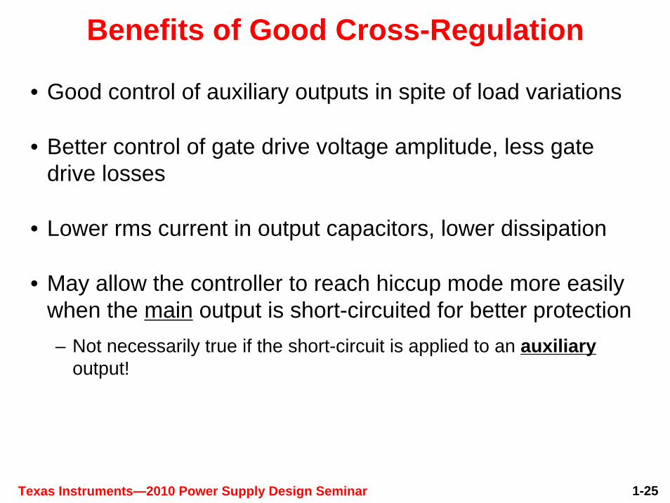
Benefits of Good Cross-Regulation
• Good control of auxiliary outputs in spite of load variations
• Better control of gate drive voltage amplitude, less gate drive losses
• Lower rms current in output capacitors, lower dissipation
• May allow the controller to reach hiccup mode more easily when the main output is short-circuited for better protection– Not necessarily true if the short-circuit is applied to an auxiliary
output!

Texas Instruments—2010 Power Supply Design Seminar 1-26
How Cross-Regulation can be Improved• The high current winding must have the best coupling to primary
• Minimize leakage between all secondary windings
• Optimize, not minimize, the leakage inductance of auxiliary windings to primary
• Use winding placement to control leakage inductance– Winding stackup– Spread each winding over the full width of the bobbin for better coupling
• Operate main output in CCM
• Try to avoid operating the auxiliary outputs in DCM. In some cases, consider using resistance in series with the diode
• Consider winding more than one auxiliary secondary simultaneously (multifilar)
• Lower clamp voltage may help– Trade-off between cross regulation, efficiency, peak drain voltage and current limit– Some other types of clamp circuits may provide better results than the RCD clamp
Prim
ary
A
Prim
ary
A
Prim
ary
A
Prim
ary
B
Prim
ary
B
Prim
ary
B
W2A
W2A
W2A
W2B
W2B
W2BW3
W3
W3or Better
than
If W3 is lightlyloaded and W2
is the high-current main
output.
Texas Instruments—2010 Power Supply Design Seminar 1-27
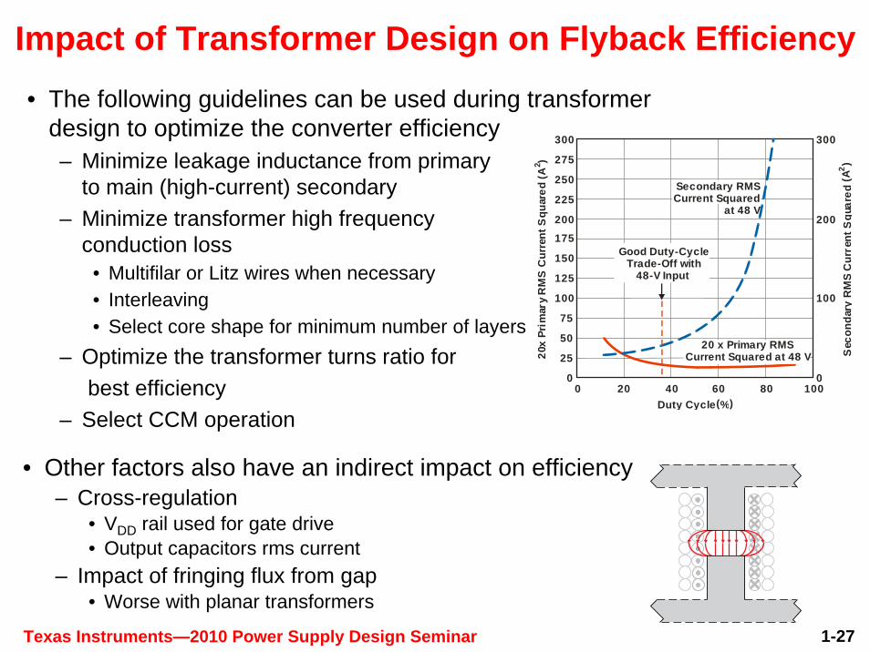
Impact of Transformer Design on Flyback Efficiency• The following guidelines can be used during transformer
design to optimize the converter efficiency– Minimize leakage inductance from primary
to main (high-current) secondary– Minimize transformer high frequency
conduction loss• Multifilar or Litz wires when necessary• Interleaving• Select core shape for minimum number of layers
– Optimize the transformer turns ratio forbest efficiency
– Select CCM operation
300
275
250
225
200
175
150
125
100
75
50
25
0
300
200
100
00 20 80 10040 60
Duty Cycle (%)
20x
Prim
ary
RM
S C
urre
nt S
quar
ed (A
)2
Sec
onda
ry R
MS
Cur
rent
Squ
ared
(A)2
Secondary RMSCurrent Squared
at 48 V
20 x Primary RMSCurrent Squared at 48 V
Good Duty-CycleTrade-Off with
48-V Input
• Other factors also have an indirect impact on efficiency– Cross-regulation
• VDD rail used for gate drive• Output capacitors rms current
– Impact of fringing flux from gap• Worse with planar transformers
Texas Instruments—2010 Power Supply Design Seminar 1-28
Flyback and EMI• Flyback ⇒ IP and IS pulsate
– Use low Z caps, minimize loop areas – Output filter often required
• Interwinding capacitance ⇒ CM CE
• Transformer and diode configuration impact effective capacitance– Less if facing windings at same AC
potential– Diode versus synchronous rectifier– Flyback ≠ Forward
Oth
erSe
cond
ary
Seco
ndar
yB
Seco
ndar
yA
FET
VD +
–Vout
+Vi
y
Prim
ary
CPr
imar
yB
Prim
ary
A
–
++
+
––Clamp
Vi VoutVD
IDM
ICM2
ICM2
FET
P S
N1:N2
Output toChassis CM
IP IS
• Better to start with end connected to primary MOSFET– Shields Vdrain E-field– Reduces interwinding capacity effect on CE
• Minimize leakage for low H-field RE
• Interleaving reduces H-field RE but may increase effective P-S interwinding capacitance
• Center-gap transformer

Texas Instruments—2010 Power Supply Design Seminar 1-29
Agenda
1. Basics of Flyback Topology
2. Impact of Transformer Design on Power Supply Performance
3. Power Supply Current Limiting
4. Summary

Texas Instruments—2010 Power Supply Design Seminar 1-30
Power Supply Current Limiting – Overview
• Current-limiting characteristic of power supply defines:– Output power beyond which output voltage falls out
of regulation. Corresponds to the “output load-current limit” (Iout_LIM)
– Output current in overload situations• including short-circuits
• Current-limiting characteristic is influenced by parasitics– Turn-off delays, leakage inductance,…

Texas Instruments—2010 Power Supply Design Seminar 1-31
Understanding Current Limit –Flyback Power Supply with Peak CMC in CCM
• Ipk_LIM is the primary peak current limit
• Io_avg is the output current
• If short-circuit, Io_avg can be much higher than when current limit has just been reached
Just at Current Limit, Output Begins to Fall Out of Regulation
Output Short Circuit
Time (t)
Time (t)
Ipk_LIM
Ipk_LIM
IA _LIM
PrimaryCurrent
PrimaryCurrent
m2S
SecondaryCurrent
SecondaryCurrent
Io_avg
Io_avg
ΔILD x Ts
(1 – D) x Ts
(1 – D) x Ts
D x Ts
( )Aout o _ avg
2
II I 1 Dn
= = × −
Power Supply Controller
PWM
COMP(From Error
Amp)
Clock Ramp
I_SENSE
+Vi Io
Iout
Vo
VC
VC_LIM
Clamp
R s
R
C
Slope Comp
RSC
1:n2
Current-SenseFilter
+
–
Texas Instruments—2010 Power Supply Design Seminar 1-32
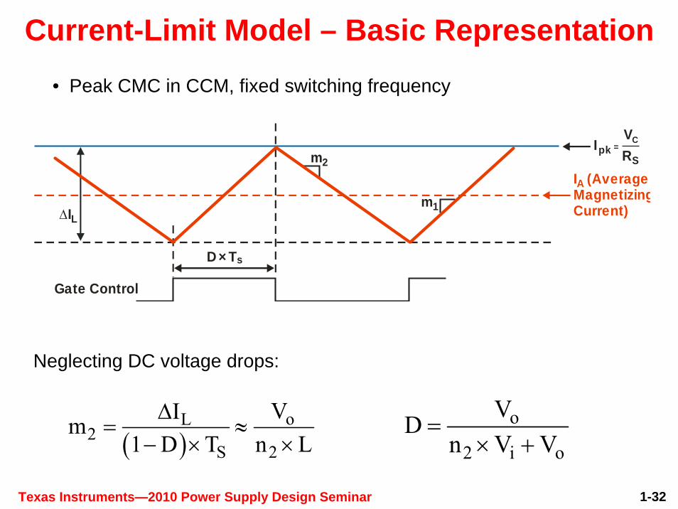
Current-Limit Model – Basic Representation• Peak CMC in CCM, fixed switching frequency
Gate Control
ΔIL
D × Ts
m2
m1
I (Average MagnetizingCurrent)
A
VCIRpk
S=
( )oL
2S 2
VIm1 D T n L
Δ= ≈
− × ×o
2 i o
VDn V V
=× +
Neglecting DC voltage drops:
Texas Instruments—2010 Power Supply Design Seminar 1-33
20 25 3530 40 45 50 55Input Voltage (V)
Out
put L
oad
Cur
rent
Lim
it (A
)
10
9
8
7
6
5
With Feedforward
Without Feedforward
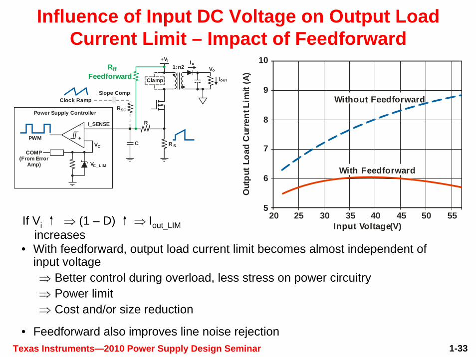
Influence of Input DC Voltage on Output Load Current Limit – Impact of Feedforward
• With feedforward, output load current limit becomes almost independent of input voltage⇒ Better control during overload, less stress on power circuitry ⇒ Power limit⇒ Cost and/or size reduction
• Feedforward also improves line noise rejection
Power Supply Controller
PWM
COMP(From Error
Amp)
Clock Ramp
I_SENSE
+Vi Io
Iout
Vo
VC
VC_LIM
Clamp
R s
R
C
Slope Comp
RSC
1:n2
+
–
FeedforwardRff
If Vi ↑ ⇒ (1 – D) ↑ ⇒ Iout_LIMincreases

Texas Instruments—2010 Power Supply Design Seminar 1-34
Current Limit Model – With Feedforward
• Kff x Vi is the feedforward contribution– Subtracting it from Vc is identical to adding it to current feedback
Gate Control
D × Ts
R × Magnetizing
Current)
S
R × mS 2R × IpkS
R × IASR × mS 1
K × Vff i
VC
Texas Instruments—2010 Power Supply Design Seminar 1-35
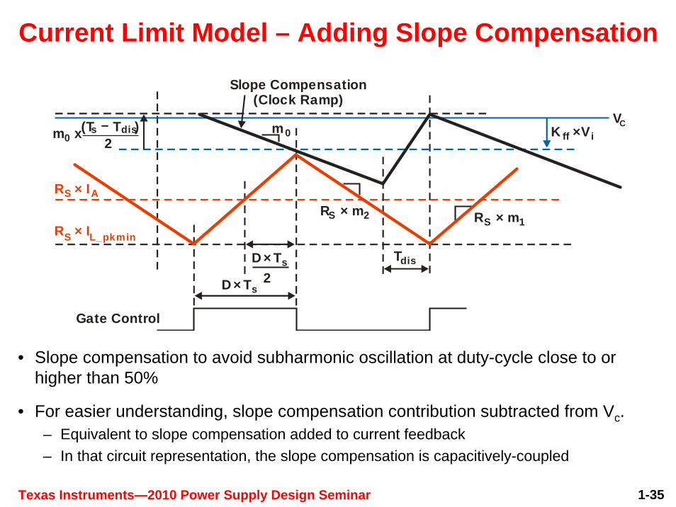
Current Limit Model – Adding Slope Compensation
• Slope compensation to avoid subharmonic oscillation at duty-cycle close to or higher than 50%
• For easier understanding, slope compensation contribution subtracted from Vc.– Equivalent to slope compensation added to current feedback– In that circuit representation, the slope compensation is capacitively-coupled
Gate Control
D × T2
s
R × mS 2 R × mS 1
VCm0
D × Ts
Tdis
R × IL_pkminS
R × IAS
K Vff i×
Slope Compensation (Clock Ramp)
m x0 2(T – T )s dis
Texas Instruments—2010 Power Supply Design Seminar 1-36
Current Limit Model – With all Delays, Slope Compensation and Feedforward
• For a more accurate, parasitics must be included in the analysis
• Parasitic delays– RC filter time delay– Turn off delay, including current comparator and gate drive – FET turn-on delay from onset of slope compensation ramp
• See Topic 1, Appendix A, in the Seminar Manual for detailed equations

Texas Instruments—2010 Power Supply Design Seminar 1-37
Influence of Transformer Leakage on Output Load Current Limit
• Rate of rise of current is influenced by leakage, commutation primary-to-secondary is not instantaneous⇒ Loss of volt-seconds (also influenced
by the clamp voltage)⇒ Duty-cycle and average magnetizing
current have to increase to maintain the output voltage
⇒ Higher conduction loss⇒ Higher transformer peak current than
expected-> Iout_LIM lower than expected
• Leakage inductance helps however to keep control of the output current in output short-circuit situation
( )oi new clamp tr new tr
2
VV D V D 1 D Dn
× ≈ × + × − −
Lleak2
Clamp+Vi
IP
+
+–+
+–
–
–Vmag1 Vmag2Lm
VDVleak2
FET
Vout
+
–
Ideal XfmrN1:N2
IS
IP
IS
Lost Volt-SecondsDtr
Texas Instruments—2010 Power Supply Design Seminar 1-38
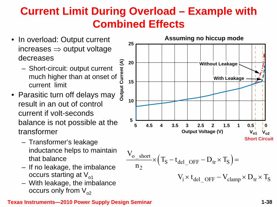
Current Limit During Overload – Example with Combined Effects
• In overload: Output current increases ⇒ output voltage decreases– Short-circuit: output current
much higher than at onset of current limit
• Parasitic turn off delays may result in an out of control current if volt-seconds balance is not possible at the transformer– Transformer’s leakage
inductance helps to maintain that balance
– If no leakage, the imbalance occurs starting at Vo1
– With leakage, the imbalance occurs only from Vo2
Assuming no hiccup mode
( )o _ shortS del _ OFF tr S
2
i del _ OFF clamp tr S
VT t D T
n V t V D T
× − − × =
× − × ×
00.511.522.533.544.555
10
15
20
25
Vo1 Vo2Output Voltage (V)Short Circuit
Out
putC
urre
nt(A
)
Without Leakage
With Leakage
Texas Instruments—2010 Power Supply Design Seminar 1-39
Summary• The flyback power transformer is the key element of the
converter, for optimum efficiency and cross-regulation
• Parasitics have a strong influence on flyback converter’s behavior, particularly under overload or short-circuit conditions
• The primary clamp circuit design is a trade-off between:– Efficiency – Peak drain voltage– Output current limit – Cross-regulation
• Simple feedforward technique can be used to optimize the converter and the system, lowering worst-case components stress and reducing the overall cost and size