UM10466 UBA2015P reference design 230 V (AC) · 2.2 nF 250 V F1 FUSE HOLDER 20 × 5 mm F3 fuse...
18
UM10466 UBA2015P reference design 230 V (AC) Rev. 1.2 — 14 November 2011 User manual Document information Info Content Keywords UBA2015P, 2 x 28W/35W T5 fluorescent lamp ballast Abstract This document describes the UBA2015P reference design for 230 V (AC).
Transcript of UM10466 UBA2015P reference design 230 V (AC) · 2.2 nF 250 V F1 FUSE HOLDER 20 × 5 mm F3 fuse...

UM10466UBA2015P reference design 230 V (AC)Rev. 1.2 — 14 November 2011 User manual
Document information
Info Content
Keywords UBA2015P, 2 x 28W/35W T5 fluorescent lamp ballast
Abstract This document describes the UBA2015P reference design for 230 V (AC).

NXP Semiconductors UM10466UBA2015P reference design 230 V (AC)
Revision history
Rev Date Description
v.1.2 20111114 third issue
v.1.1 20110704 second issue
v.1 20110503 first issue
UM10466 All information provided in this document is subject to legal disclaimers. © NXP B.V. 2011. All rights reserved.
User manual Rev. 1.2 — 14 November 2011 2 of 18
Contact informationFor more information, please visit: http://www.nxp.com
For sales office addresses, please send an email to: [email protected]

NXP Semiconductors UM10466UBA2015P reference design 230 V (AC)
1. Introduction
This document describes the specification and use of the UBA2015P board. This reference ballast design is intended to drive two TL5HE28W or TL5HE35W lamps.
Do not power the board without IC; the VDD decoupling capacitor voltage exceeds the rated value when the IC does not limit the voltage to 13 V.
2. Safety warning
The board needs to be connected to the mains voltage. Touching the board while it is connected to the mains voltage must be avoided at all times. An isolated housing is obligatory when used in uncontrolled, non laboratory environments. Galvanic isolation of the mains phase using a variable transformer is always recommended.
Fig 1. UBA2015P reference board
019aac298
WARNING
Lethal voltage and fire ignition hazard
The non-insulated high voltages that are present when operating this product, constitute a risk of electric shock, personal injury, death and/or ignition of fire.
This product is intended for evaluation purposes only. It shall be operated in a designated test area by personnel qualified according to local requirements and labor laws to work with non-insulated mains voltages and high-voltage circuits. This product shall never be operated unattended.
a. Isolated b. Not isolated
Fig 2. Variac isolation symbols
019aab173 019aab174
UM10466 All information provided in this document is subject to legal disclaimers. © NXP B.V. 2011. All rights reserved.
User manual Rev. 1.2 — 14 November 2011 3 of 18

NXP Semiconductors UM10466UBA2015P reference design 230 V (AC)
3. Specifications
4. Board information
4.1 Block diagram
The input section includes:
• The fuse
• Surge protection against fast AC transients
• ElectroMagnetic Interference (EMI) filter
• Full-wave rectifier
• Preconditioner or Power Factor Correction (PFC)
The output of the PFC connects to a electrolytic buffer capacitor to supply the half-bridge circuit. The lamp connects to the half-bridge circuit. The UBA2015P controller IC controls the PFC and the half-bridge circuit.
The PFC is implemented as an up converter in boundary conduction mode. The resonant circuit is voltage fed by the half-bridge which consists of two N-channel MOSFETs. The resonant circuit includes a transformer for electrode (pre)heating.
Table 1. Electrical board specification
Description Product(s)
Ballast type electronic
Starting method programmed start with preheat
Starting time < 1 s
Lamp terminals 7
Lamp connection parallel
Line voltage 220 V (AC) to 240 V (AC)
Line frequency 50 Hz/60 Hz
Number of lamps 2
Dimming interface none
Transient protection compatibility IEC61547
Table 2. Supported lamps
Lamp type Description
35W T5 35 W T5 high-efficiency fluorescent lamp
28W T5 28 W T5 high-efficiency fluorescent lamp
Table 3. Ballast performance
Lamp type Number of lamps
Rated lamp power (W)
Maximum THD (%)
Maximum lamp current crest factor
Power factor Nominal lamp current (A)
35W T5 2 35 10 1.7 0.98 0.170
28W T5 2 28 10 1.7 0.97 0.170
UM10466 All information provided in this document is subject to legal disclaimers. © NXP B.V. 2011. All rights reserved.
User manual Rev. 1.2 — 14 November 2011 4 of 18

NXP Semiconductors UM10466UBA2015P reference design 230 V (AC)
This type of topology with inductive heating is used in many commercial ballasts whose power exceeds 25 W, making it a cost-effective application.
The lamps are connected in parallel.
4.2 Performance indicators
4.2.1 Input power, power factor and Total Harmonic Distortion (THD)
4.2.2 Lamp end of life detection
IEC asymmetrical power test: The End-Of-Life (EOL) resistor REOL is increased (manually controlled rheostat of 1 k) until the ballast shuts down. A rheostat is a two-terminal variable resistor. See IEC-61347-2-3 Section 17.3 where this test is described. When the EOL voltage exceeds the thresholds of the internal window comparator the slow fault timer (CPT pin) starts.
Fig 3. Block diagram
019aac299
mainsvoltageinput
FUSE SURGEPROT
EMIFILTER
ACRECTIFIER PFC BUFFER
CAPHALF
BRIDGERESONANT
CIRCUIT
UBA2015CONTROLLER
lamps
Measured with a dummy lamp (resistors only)
(1) Power factor
(2) Current THD
(3) Input power (W)
Fig 4. THD, power factor and input power as a function of AC mains input voltage
Mains voltage (V)180 280260220 240200
019aac290
0.4
0.6
0.2
0.8
1.0
0
75.2
75.4
75.0
75.8
75.6
76.0Power
(W)
74.8
(1)
(3)
(2)
Power factor,THD
UM10466 All information provided in this document is subject to legal disclaimers. © NXP B.V. 2011. All rights reserved.
User manual Rev. 1.2 — 14 November 2011 5 of 18

NXP Semiconductors UM10466UBA2015P reference design 230 V (AC)
Measurements: P2 = Mean(PEOL) between divisions 4 and 5 on the plot
Traces:
(1) C1 = Z1 = EOL
(2) C2 = Z2 = CPT
(3) F1 = F2 P(REOL
Fig 5. EOL shutdown triggered by Vth(low)EOL
019aac291
UM10466 All information provided in this document is subject to legal disclaimers. © NXP B.V. 2011. All rights reserved.
User manual Rev. 1.2 — 14 November 2011 6 of 18

NXP Semiconductors UM10466UBA2015P reference design 230 V (AC)
4.2.3 Lamp removal detection
The UBA2015/UBA2016 family has several fast protection features for lamp removal detection:
• Capacitive Mode Protection (CMP)
• Saturation protection
• OverVoltage Protection (OVP)
In this application the overvoltage protection is triggered during lamp removal. Other applications with a different operating frequency with respect to the resonance frequency can be triggered differently. The main function of the IC is to shut down as fast as possible when a lamp is removed.
The fast protection on the VFB pin is repeatedly triggered (VVFB > 3.35 V (typical)) during the lamp removal process and as a result the fast fault detection timer tdet(fault) ends.
In this application the shutdown is not triggered by pin SLHB because of the 340 ns leading edge blanking time on this pin.
Measurements: P2 = Mean(Peol) between divisions 4 and 5 on the plot
Traces:
(1) C1 = Z1 = EOL
(2) C2 = Z2 = CPT
(3) F1 = F2 P(REOL)
Fig 6. EOL shutdown triggered by Vth(high)EOL
019aac292
UM10466 All information provided in this document is subject to legal disclaimers. © NXP B.V. 2011. All rights reserved.
User manual Rev. 1.2 — 14 November 2011 7 of 18

NXP Semiconductors UM10466UBA2015P reference design 230 V (AC)
(1) C1 = Z1 = GLHB
(2) C2 = Z2 = SLHB
(3) C3 = Z3 = VFB
(4) C4 = Z4 = SHHB
Fig 7. Shutdown after lamp removal triggered by Vth(ov)(VFB)
019aac293
UM10466 All information provided in this document is subject to legal disclaimers. © NXP B.V. 2011. All rights reserved.
User manual Rev. 1.2 — 14 November 2011 8 of 18
NXP Semiconductors UM10466UBA2015P reference design 230 V (AC)
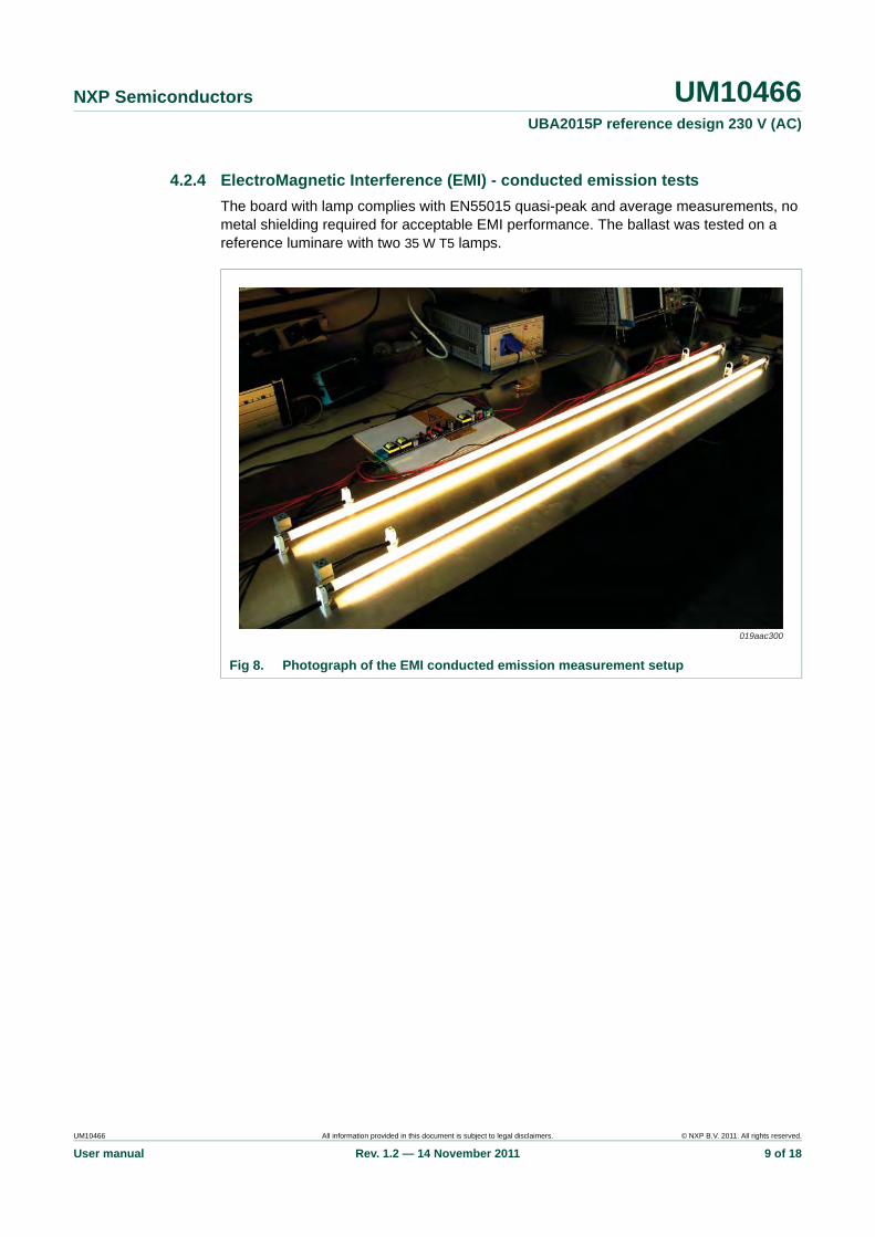
4.2.4 ElectroMagnetic Interference (EMI) - conducted emission tests
The board with lamp complies with EN55015 quasi-peak and average measurements, no metal shielding required for acceptable EMI performance. The ballast was tested on a reference luminare with two 35 W T5 lamps.
Fig 8. Photograph of the EMI conducted emission measurement setup
019aac300
UM10466 All information provided in this document is subject to legal disclaimers. © NXP B.V. 2011. All rights reserved.
User manual Rev. 1.2 — 14 November 2011 9 of 18

NXP Semiconductors UM10466UBA2015P reference design 230 V (AC)
a. Line L
b. Line N
Fig 9. EMI: conducted emission test results
019aac294
019aac295
UM10466 All information provided in this document is subject to legal disclaimers. © NXP B.V. 2011. All rights reserved.
User manual Rev. 1.2 — 14 November 2011 10 of 18

NXP Semiconductors UM10466UBA2015P reference design 230 V (AC)
5. Wiring diagram
The ballast must be connected as shown in Figure 10.
The chassis must be connected to ground which is available on mounting hole E1.
Keep the hot wires to the lamps as short as possible (red and blue wires), so parasitic capacitance remains as low as possible.
Fig 10. Wiring diagram
019aac296
BALLAST
J2-7RED
J2-6RED
GREEN/YELLOWJ1-1
BLACKJ1-2
WHITEJ1-3
protective ground
hot
neutral
J2-5BLUE
J2-4BLUE
J2-3BLACK
J2-2GREEN
J2-1GREEN
LAMP
LAMP
UM10466 All information provided in this document is subject to legal disclaimers. © NXP B.V. 2011. All rights reserved.
User manual Rev. 1.2 — 14 November 2011 11 of 18

xxxx xxxxxxxxxxxxxxxxxxxxxxxxxxxxxx x xxxxxxxxxxxxxx xxxxxxxxxx xxx xxxxxx xxxxxxxxxxxxxxxxxxxxxxx xxxxxxxxxxxxxxxxxxxxxx xxxxx xxxxxx xx xxxxxxxxxxxxxxxxxxxxxxxxxxxxx xxxxxxxxxxxxxxxxxxxxxx xxxxxxxxxxx xxxxxxx xxxxxxxxxxxxxxxxxxx xxxxxxxxxxxxxxxx xxxxxxxxxxxxxx xxxxxx xx xxxxxxxxxxxxxxxxxxxxxxxxxxxxxxxx xxxxxxxxxxxxxxxxxxxxxxxx xxxxxxx xxxxxxxxxxxxxxxxxxxxxxxxxxxxxxxxxxxxxxxxxxxxxx xxxxxxxxxxx xxxxx x x
UM
10466
User m
anu
al
NX
P S
emico
nd
ucto
6. S
chem
atic
R1F2 T1A
TMP-3094
rsU
M10466
UB
A2
015
P re
fere
nce
de
sign
230 V
(AC
)
019aac301
kΩ
MΩ
15
C18 nF
J2
X2
LAM
P
330 kΩ
R14
X4
10
4
7X56X65X74X83X92X101
1 2
3 4
7
6
5
4
3
2
1
VDD
X1
LAM
P
1 2
3 4
All inform
ation provided in this docum
ent is subject to legal disclaim
ers.©
NX
P B
.V. 20
11. All rights reserved
.
Rev. 1.2 —
14 No
vem
ber 2011
12 o
f 18 Fig 11. Schematic diagram
330 kΩ
R20.82 Ω
Q12SK3567
R33.48 kΩ
R18180 kΩ
R201 kΩ
R12464
R191 kΩ
D131N4937
D121N4937
41.2 kΩ
41.2 kΩ
R221 MΩ
R131 Ω
R4562 kΩ
R5562 kΩ
R21
C1
D14
nm
D6
1N4118
R16
10
R
L3A7608000901
3.9 mH
R17
D11
1N4148 D10
1N4148
D5
UF4006
X3
2.2 nF250 V
F1
FUSE HOLDER20 × 5 mm
F3 fuse holder cover,20 × 5 mm
V1710 V
C2220 nF
C2147 nF
C15100 nF 220
C2047 nF
C192.7 nF
C222.7 nF
C410 nF
D31N4007
D11N4007
C3470 nF
C141 nF
D41N4007
D21N4007
C522 μF
Q22SK3567
WB1
1
3
6mains N
4
L1
2 × 10 mH
1
10
481 109
AUXPFCGND
GND
GND
8
T2A
T2B1.8 mH
C27220 nF
4.7 Ω
J1
STARTUP
GPFC
GHHB
SHHB
VFB
FBPFC
1
2
3
82 kΩ
R11
33 kΩ
R10
X11GND
jumperlink
1 kΩ
R8
10 kΩ
R6
nm
R7
D71N5244B
C7470 nF
C61 nF
390 kΩ
R9
C16
82 nF C13
200 pFC17
100 nF
C11
100 nF
E13.5 mm
E2 E3 E4
mounting hole3.5 mm non plated
E5 E6
C9
D9
1N4148
D8
1N4148
100 nF
C8
2.2 nFC12
68 nF C10
22 nF
UBA2015Pin socket
GND
GNDGND
GND
GND
U1
11PH/ENFBPFC
FBPFCAUXPFC
AUXPFC
10
12n.c.COMPPFC
9
13CPTAUXPFC
8
14CFGPFC
GPFC 7
15CIFBGND
6
16IREFVDD
VDD 5
17VFBGLHB
GLHB 4
18EOLSHHB
SHHB 3
19IFBFSHB
2
20SLHB
VFB
EOL
SLHBGHHB
GHHB 1
U
X1
X2 mains L
TMP-3093
chassis
L4C
9 μH
C2368 nF
9
L3C
9 μH
45 L4B
9 μH
5 L3B
9 μH
C2568 nF
C2668 nF
C2468 nF
L4A7608000901
3.9 mH 81Q3
2SK3567GLHB
SLHB
STARTUP
EOL

xxxxxxxxxxxxxxxxxxxxx xxxxxxxxxxxxxxxxxxxxxxxxxx xxxxxxx x x x xxxxxxxxxxxxxxxxxxxxxxxxxxxxxx xxxxxxxxxxxxxxxxxxx xx xx xxxxx xxxxxxxxxxxxxxxxxxxxxxxxxxx xxxxxxxxxxxxxxxxxxx xxxxxx xxxxxxxxxxxxxxxxxxxxxxxxxxxxxxxxxxx xxxxxxxxxxxx x x xxxxxxxxxxxxxxxxxxxxx xxxxxxxxxxxxxxxxxxxxxxxxxxxxxx xxxxx xxxxxxxxxxxxxxxxxxxxxxxxxxxxxxxxxxxxxxxxxxxxxxxxxx xxxxxxxx xxxxxxxxxxxxxxxxxxxxxxxxx xxxxxxxxxxxxxxxxxxxx xxx
UM
10466
User m
anu
al
NX
P S
emico
nd
ucto
rsU
M10466
UB
A2
015
P re
fere
nce
de
sign
230 V
(AC
)
7. PCB layout
019aac297
All inform
ation provided in this docum
ent is subject to legal disclaim
ers.©
NX
P B
.V. 20
11. All rights reserved
.
Rev. 1.2 —
14 No
vem
ber 2011
13 o
f 18
Fig 12. PCB layout

NXP Semiconductors UM10466UBA2015P reference design 230 V (AC)
8. Bill of materials
Table 4. Bill of materials
Item number
Part reference
Description/value Manufacturer Part number
1 C1 2.2 nF; 20 %; 250 V Murata DE1E3KX222MA5B
2 C2 100 nF; 10 %; 275 V Vishay BFC233912104
3 C3 220 nF; 10 %; 400 V Xicon 146-MEF2G224K
4 C4 10 nF; 20 %, +80 %; 50 V Vishay K103Z15Y5VF5TH5
5 C5 22 F; 20 %; 450 V Panasonic EEU-EB2W220S
6 C6 1 nF; 10 %; 500 V Vishay H102K25X7RL63J5R
7 C7 470 nF; 5 %; 63 V Kemet R82DC3470DQ60J
8 C8 2.2 nF; 10 %; 100 V Multicomp MCRR50222X7RK0100
9 C9 100 nF; 10 %; 100 V Vishay BFC236525104
10 C10 22 nF; 10 %; 100 V BC components 2222 370 21223
11 C11 100 nF; 10 %; 100 V Vishay BFC236525104
12 C12 68 nF; 5 %; 63 V Kemet MMK5683K63J01L16.5TA182
13 C13 200 pF; 5 %; 100 V Multicomp MC0805N201J101A2.54MM
14 C14 1 nF; 10 %; 50 V Vishay K102K15X7RF5TH5
15 C15 100 nF; 10 %; 100 V Vishay BFC236525104
16 C16 82 nF; 5 %; 63 V Kemet MMK5823M63J01L4BULK
17 C17 100 nF; 10 %; 100 V Vishay BFC236525104
18 C18 220 nF; 10 %; 400 V Xicon 146-MEF2G224K
19 C19 2.7 nF; 5 %; 2000 V Vishay BFC238361272
20 C20 47 nF; 5 %; 100 V Kemet R82EC2470AA60J
21 C21 47 nF; 5 %; 100 V Kemet R82EC2470AA60J
22 C22 2.7 nF; 5 %; 2000 V Vishay BFC238361272
23 C23 68 nF; 10 %; 400 V Epcos B32521C6683K
24 C24 68 nF; 10 %; 400 V Epcos B32521C6683K
25 C25 68 nF; 10 %; 400 V Epcos B32521C6683K
26 C26 68 nF; 10 %; 400 V Epcos B32521C6683K
27 C27 100 nF; 10 %; 275 V Vishay BFC233912104
28 D1 1N4007-E3/51 Vishay 1N4007-E3/51
29 D2 1N4007-E3/51 Vishay 1N4007-E3/51
30 D3 1N4007-E3/51 Vishay 1N4007-E3/51
31 D4 1N4007-E3/51 Vishay 1N4007-E3/51
32 D5 UF4006-E3/73 Vishay UF4006-E3/73
33 D6 1N4148 NXP Semiconductors 1N4148,133
34 D7 1N5244B Fairchild Semiconductor 1N5244B
35 D8 1N4148 NXP Semiconductors 1N4148,133
36 D9 1N4148 NXP Semiconductors 1N4148,133
37 D10 1N4148 NXP Semiconductors 1N4148,133
38 D11 1N4148 NXP Semiconductors 1N4148,133
UM10466 All information provided in this document is subject to legal disclaimers. © NXP B.V. 2011. All rights reserved.
User manual Rev. 1.2 — 14 November 2011 14 of 18

NXP Semiconductors UM10466UBA2015P reference design 230 V (AC)
39 D12 1N4937/54; 600 V; 1 A Vishay 1N4937-E3/54
40 D13 1N4937/54; 600 V; 1 A Vishay 1N4937-E3/54
41 D14 1N4007-E3/51 Vishay 1N4007-E3/51
42 F1 fuse holder; 20 5 mm Multicomp MCHTC-15M
43 F2 fuse T1A Schurter 34.3117
44 F3 fuse holder cover; 20 5 mm Multicomp MCHTC-150M
45 J1 PCB mounted screw terminal MKDSN2,5/3-5.08
Phoenix Contact 1888690
46 J2 PCB mounted screw terminal MKDS 1/7-3,81
Phoenix Contact 1727065
47 L1 B82731T2102A020; 2 10 mH Epcos B82731T2102A020
48 L3 Transformer; 3.9 mH; 9 H; 9 H
Würth ElektroniK 7608000901
49 L4 Transformer; 3.9 mH; 9 H; 9 H
Würth ElektroniK 7608000901
50 Q1 2SK3567 Toshiba 2SK3567
51 Q2 2SK3567 Toshiba 2SK3567
52 Q3 2SK3567 Toshiba 2SK3567
53 R1 330 k; 5 %; 2 W Welwyn MFP2-330K J1
54 R2 0.82 ; 5 %; 1 W; 400 V KOA Speer MOSX1/2CT52RR82J
55 R3 3.48 k; 1 %; 0.6 W Vishay MRS25000C3481FCT00
56 R4 562 k; 1 %; 0.6 W Vishay MRS25000C5623FCT00
57 R5 562 k; 1 %; 0.6 W Vishay MRS25000C5623FCT00
58 R6 10 k; 1 %; 0.25 W Xicon 271-10K-RC
59 R7 1 k; 1 %; 0.25 W Xicon 271-1K-RC
60 R8 1 k; 1 %; 0.25 W Xicon 271-1K-RC
61 R9 390 k; 1 %; 0.25 W Xicon 271-390K-RC
62 R10 33 k; 1 %; 0.25 W Xicon 271-33K-RC
63 R11 82 k; 1 %; 0.6 W Vishay MRS25000C8202FCT00
64 R12 140 k; 1 %; 0.6 W Vishay MRS25000C1403FCT00
65 R13 1 ; 5 %; 1 W; 400 V KOA Speer MOSX1/2CT52R1R0J
66 R14 330 k; 5 %; 2 W Welwyn MFP2-330K J1
67 R15 6.8 M; 1 %; 0.6 W Vishay MRS25000C6804FCT00
68 R16 41.2 k; 1 %; 0.25 W Xicon 271-41.2K-RC
69 R17 41.2 k; 1 %; 0.25 W Xicon 271-41.2K-RC
70 R18 180 k; 1 %; 0.6 W Vishay MRS25000C1803FCT00
71 R19 1 k; 1 %; 0.25 W Xicon 271-1K-RC
72 R20 1 k; 1 %; 0.25 W Xicon 271-1K-RC
73 R21 4.7 ; 20 %; 1.4 W Epcos B57153S479M
74 R22 1 M; 1 %; 0.6 W Vishay MRS25000C1004FCT00
75 T2 Transformer 760801095 Würth ElektroniK 760801095
Table 4. Bill of materials …continued
Item number
Part reference
Description/value Manufacturer Part number
UM10466 All information provided in this document is subject to legal disclaimers. © NXP B.V. 2011. All rights reserved.
User manual Rev. 1.2 — 14 November 2011 15 of 18

NXP Semiconductors UM10466UBA2015P reference design 230 V (AC)
76 U1 UBA2015P NXP Semiconductors UBA2015P
77 V1 275 V (AC); 85 C; 3.5 kA; 710 Vclamp
Littelfuse V10E275P
78 WB1 wire-bridge-4E 3M 923345-04
79 X11 jumper link Fischer Elektro LB 03 G
Table 4. Bill of materials …continued
Item number
Part reference
Description/value Manufacturer Part number
UM10466 All information provided in this document is subject to legal disclaimers. © NXP B.V. 2011. All rights reserved.
User manual Rev. 1.2 — 14 November 2011 16 of 18

NXP Semiconductors UM10466UBA2015P reference design 230 V (AC)
9. Legal information
9.1 Definitions
Draft — The document is a draft version only. The content is still under internal review and subject to formal approval, which may result in modifications or additions. NXP Semiconductors does not give any representations or warranties as to the accuracy or completeness of information included herein and shall have no liability for the consequences of use of such information.
9.2 Disclaimers
Limited warranty and liability — Information in this document is believed to be accurate and reliable. However, NXP Semiconductors does not give any representations or warranties, expressed or implied, as to the accuracy or completeness of such information and shall have no liability for the consequences of use of such information.
In no event shall NXP Semiconductors be liable for any indirect, incidental, punitive, special or consequential damages (including - without limitation - lost profits, lost savings, business interruption, costs related to the removal or replacement of any products or rework charges) whether or not such damages are based on tort (including negligence), warranty, breach of contract or any other legal theory.
Notwithstanding any damages that customer might incur for any reason whatsoever, NXP Semiconductors’ aggregate and cumulative liability towards customer for the products described herein shall be limited in accordance with the Terms and conditions of commercial sale of NXP Semiconductors.
Right to make changes — NXP Semiconductors reserves the right to make changes to information published in this document, including without limitation specifications and product descriptions, at any time and without notice. This document supersedes and replaces all information supplied prior to the publication hereof.
Suitability for use — NXP Semiconductors products are not designed, authorized or warranted to be suitable for use in life support, life-critical or safety-critical systems or equipment, nor in applications where failure or malfunction of an NXP Semiconductors product can reasonably be expected to result in personal injury, death or severe property or environmental damage. NXP Semiconductors accepts no liability for inclusion and/or use of NXP Semiconductors products in such equipment or applications and therefore such inclusion and/or use is at the customer’s own risk.
Applications — Applications that are described herein for any of these products are for illustrative purposes only. NXP Semiconductors makes no representation or warranty that such applications will be suitable for the specified use without further testing or modification.
Customers are responsible for the design and operation of their applications and products using NXP Semiconductors products, and NXP Semiconductors accepts no liability for any assistance with applications or customer product
design. It is customer’s sole responsibility to determine whether the NXP Semiconductors product is suitable and fit for the customer’s applications and products planned, as well as for the planned application and use of customer’s third party customer(s). Customers should provide appropriate design and operating safeguards to minimize the risks associated with their applications and products.
NXP Semiconductors does not accept any liability related to any default, damage, costs or problem which is based on any weakness or default in the customer’s applications or products, or the application or use by customer’s third party customer(s). Customer is responsible for doing all necessary testing for the customer’s applications and products using NXP Semiconductors products in order to avoid a default of the applications and the products or of the application or use by customer’s third party customer(s). NXP does not accept any liability in this respect.
Export control — This document as well as the item(s) described herein may be subject to export control regulations. Export might require a prior authorization from competent authorities.
Evaluation products — This product is provided on an “as is” and “with all faults” basis for evaluation purposes only. NXP Semiconductors, its affiliates and their suppliers expressly disclaim all warranties, whether express, implied or statutory, including but not limited to the implied warranties of non-infringement, merchantability and fitness for a particular purpose. The entire risk as to the quality, or arising out of the use or performance, of this product remains with customer.
In no event shall NXP Semiconductors, its affiliates or their suppliers be liable to customer for any special, indirect, consequential, punitive or incidental damages (including without limitation damages for loss of business, business interruption, loss of use, loss of data or information, and the like) arising out the use of or inability to use the product, whether or not based on tort (including negligence), strict liability, breach of contract, breach of warranty or any other theory, even if advised of the possibility of such damages.
Notwithstanding any damages that customer might incur for any reason whatsoever (including without limitation, all damages referenced above and all direct or general damages), the entire liability of NXP Semiconductors, its affiliates and their suppliers and customer’s exclusive remedy for all of the foregoing shall be limited to actual damages incurred by customer based on reasonable reliance up to the greater of the amount actually paid by customer for the product or five dollars (US$5.00). The foregoing limitations, exclusions and disclaimers shall apply to the maximum extent permitted by applicable law, even if any remedy fails of its essential purpose.
9.3 TrademarksNotice: All referenced brands, product names, service names and trademarks are the property of their respective owners.
UM10466 All information provided in this document is subject to legal disclaimers. © NXP B.V. 2011. All rights reserved.
User manual Rev. 1.2 — 14 November 2011 17 of 18

NXP Semiconductors UM10466UBA2015P reference design 230 V (AC)
10. Contents
1 Introduction . . . . . . . . . . . . . . . . . . . . . . . . . . . . 3
2 Safety warning . . . . . . . . . . . . . . . . . . . . . . . . . . 3
3 Specifications. . . . . . . . . . . . . . . . . . . . . . . . . . . 4
4 Board information . . . . . . . . . . . . . . . . . . . . . . . 44.1 Block diagram. . . . . . . . . . . . . . . . . . . . . . . . . . 44.2 Performance indicators. . . . . . . . . . . . . . . . . . . 54.2.1 Input power, power factor and Total
Harmonic Distortion (THD) . . . . . . . . . . . . . . . . 54.2.2 Lamp end of life detection . . . . . . . . . . . . . . . . 54.2.3 Lamp removal detection . . . . . . . . . . . . . . . . . . 74.2.4 ElectroMagnetic Interference (EMI)
- conducted emission tests . . . . . . . . . . . . . . . . 9
5 Wiring diagram. . . . . . . . . . . . . . . . . . . . . . . . . 11
6 Schematic. . . . . . . . . . . . . . . . . . . . . . . . . . . . . 12
7 PCB layout . . . . . . . . . . . . . . . . . . . . . . . . . . . . 13
8 Bill of materials . . . . . . . . . . . . . . . . . . . . . . . . 14
9 Legal information. . . . . . . . . . . . . . . . . . . . . . . 179.1 Definitions. . . . . . . . . . . . . . . . . . . . . . . . . . . . 179.2 Disclaimers . . . . . . . . . . . . . . . . . . . . . . . . . . . 179.3 Trademarks. . . . . . . . . . . . . . . . . . . . . . . . . . . 17
10 Contents . . . . . . . . . . . . . . . . . . . . . . . . . . . . . . 18
© NXP B.V. 2011. All rights reserved.
For more information, please visit: http://www.nxp.comFor sales office addresses, please send an email to: [email protected]
Date of release: 14 November 2011
Document identifier: UM10466
Please be aware that important notices concerning this document and the product(s)described herein, have been included in section ‘Legal information’.