UM10379 Typical 250 W LCD TV AC-DC power supply ...without flyback) 90 V / 50 Hz 5.04 V 370 mW 575...
32
UM10379 Typical 250 W LCD TV AC-DC power supply application with the TEA1713 PFC and half-bridge resonant controller Rev. 01 — 16 April 2010 User manual Document information Info Content Keywords TEA1713, half bridge, PFC controller, LLC resonant, high efficiency, zero voltage switching, resonant frequency, leakage inductance. Abstract The TEA1713 includes a PFC controller as well as a controller for a half bridge resonant converter. This user manual describes a 250 W resonant switching mode power supply for a typical LCD TV design based on the TEA1713. The board provides 3 output voltages of 24 V / 8 A, 12 V / 4 A and a standby supply of 5 V / 2 A. Good cross regulation is achieved without using a compensation circuit. It is also possible to test the Burst mode of the TEA1713. This feature is normally used in single-output resonant converters but can also be tested with this demo board by making some circuit adjustments. In Burst mode, the no load input power is around 600 mW (490 mW when the 5 V STB supply is disconnected from the PFC bus voltage) at high mains voltage. Typical efficiency at high output power is above 90 % for universal mains input with Schottky rectifiers.
Transcript of UM10379 Typical 250 W LCD TV AC-DC power supply ...without flyback) 90 V / 50 Hz 5.04 V 370 mW 575...
UM10379Typical 250 W LCD TV AC-DC power supply application with the TEA1713 PFC and half-bridge resonant controllerRev. 01 — 16 April 2010 User manual
Document informationInfo ContentKeywords TEA1713, half bridge, PFC controller, LLC resonant, high efficiency, zero
voltage switching, resonant frequency, leakage inductance.
Abstract The TEA1713 includes a PFC controller as well as a controller for a half bridge resonant converter. This user manual describes a 250 W resonant switching mode power supply for a typical LCD TV design based on the TEA1713. The board provides 3 output voltages of 24 V / 8 A, 12 V / 4 A and a standby supply of 5 V / 2 A. Good cross regulation is achieved without using a compensation circuit. It is also possible to test the Burst mode of the TEA1713. This feature is normally used in single-output resonant converters but can also be tested with this demo board by making some circuit adjustments. In Burst mode, the no load input power is around 600 mW (490 mW when the 5 V STB supply is disconnected from the PFC bus voltage) at high mains voltage. Typical efficiency at high output power is above 90 % for universal mains input with Schottky rectifiers.
NXP Semiconductors UM10379TEA1713 250 W resonant demoboard
Revision historyRev Date Description
01 20100416 First issue
UM10379_1 All information provided in this document is subject to legal disclaimers. © NXP B.V. 2010. All rights reserved.
User manual Rev. 01 — 16 April 2010 2 of 32
Contact informationFor more information, please visit: http://www.nxp.com
For sales office addresses, please send an email to: [email protected]
NXP Semiconductors UM10379TEA1713 250 W resonant demoboard
1. Introduction
The TEA1713 integrates a Power Factor Corrector (PFC) controller and a controller for a Half-Bridge resonant Converter (HBC) in a multi-chip IC. The TEA1713 250 W resonant demo board has multiple outputs so it can be used as a typical LCD TV power supply. Other target applications include plasma TV, PC power and power adapters (only a single output would be needed for an adapter). The TEA1713 Burst mode feature makes it possible to increase efficiency in the low- to mid-power range.
The demo board contains three sub-circuits:
• A PFC control stage (integrated into the TEA1713)• A HBC control stage (integrated into the TEA1713)• An additional standby supply (TEA1522)
Three regulated outputs are provided:
• 24 V / 8 A• 12 V / 4 A• 5 V / 2 A for Normal mode or 5 V / 1.5 A for Standby mode
The demo board features a number of protection functions including OverVoltage Protection (OVP), OverCurrent Protection (OCP), Short Circuit Protection (SCP) and mains UnderVoltage Protection (UVP). See the TEA1713 data sheet and the TEA1713 application note for further details.
2. Setup
2.1 Normal operationTo enable Normal mode on the demo board:
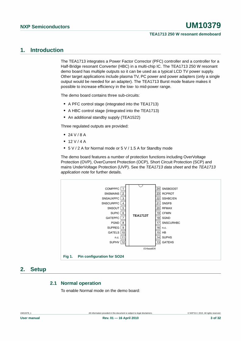
Fig 1. Pin configuration for SO24
TEA1713T
COMPPFC SNSBOOST
SNSMAINS RCPROT
SNSAUXPFC SSHBC/EN
SNSCURPFC SNSFB
SNSOUT RFMAX
SUPIC CFMIN
GATEPFC SGND
PGND SNSCURHBC
SUPREG n.c.
GATELS HB
n.c. SUPHS
SUPHV GATEHS
014aaa826
1
2
3
4
5
6
7
8
9
10
11
12
14
13
16
15
18
17
20
19
22
21
24
23
UM10379_1 All information provided in this document is subject to legal disclaimers. © NXP B.V. 2010. All rights reserved.
User manual Rev. 01 — 16 April 2010 3 of 32

NXP Semiconductors UM10379TEA1713 250 W resonant demoboard
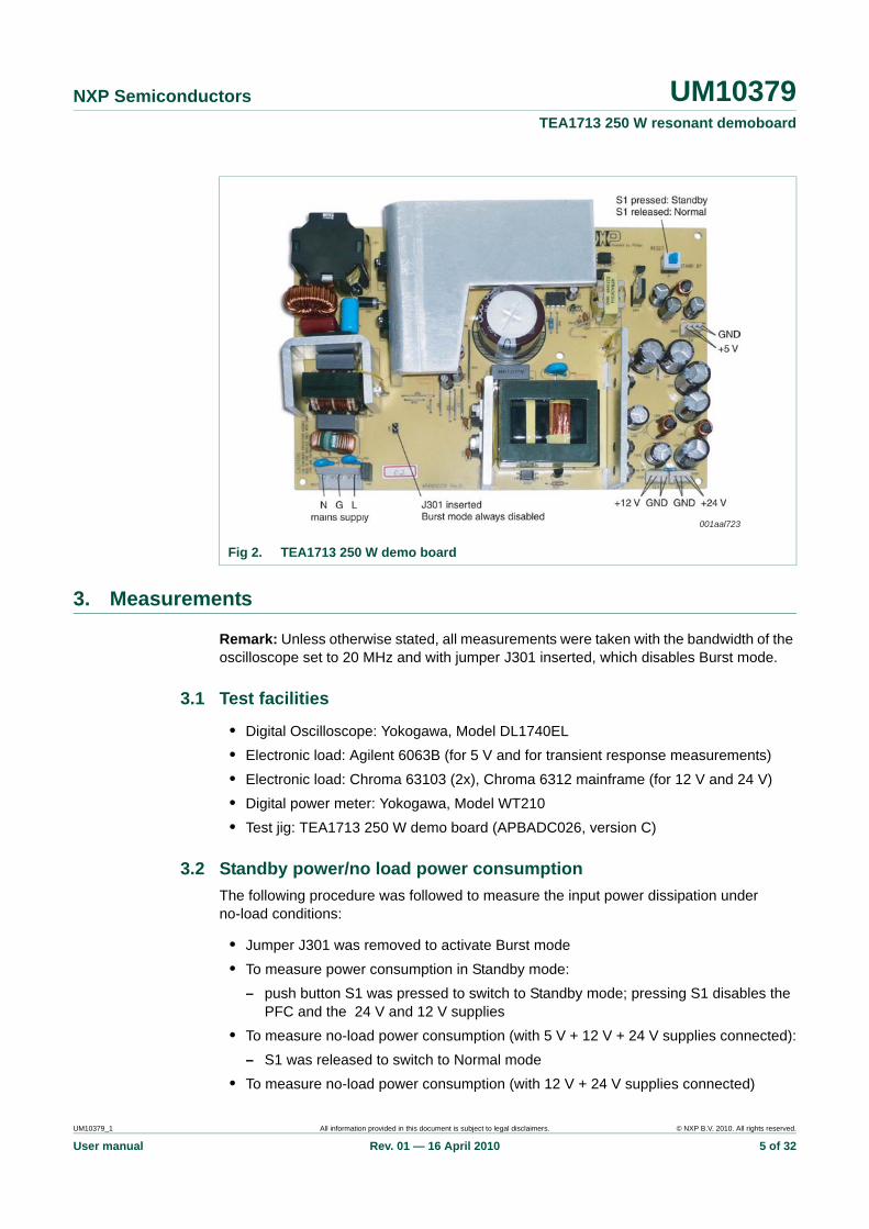
• Ensure jumper J301 is inserted to disable Burst mode; the board is designed to operate as a multiple-output board (24 V and 12 V, as well as 5 V standby); Burst mode is intended for single output solutions only (e.g. power adapters)
• Connect suitable loads at the outputs (24 V and 12 V)• A load may also be connected at the 5 V standby output• Connect the mains supply voltage VAC (90 V to 264 V (AC))
Pressing switch S1 disables the TEA1713 while keeping the 5 V standby supply operating. S1 can also be used to reset the TEA1713 after a latched protection function has been triggered.
2.2 Burst mode operationBurst mode helps to significantly increase the efficiency of the demo board at low output power levels. In the TEA1713, Burst mode is primarily intended to be used with single output power supplies. To enable Burst mode on the demo board:
• Remove jumper J301; this enables Burst mode operation for low loads• Connect a suitable load at the 24 V output; leave the 12 V output open; converter
operation now approximates that of a single output converter, although the 12 V rail still has some influence on the voltage feedback loop (see resistor R312)
• Resistor R361 may need to be fine-tuned in order to set the burst mode thresholds accurately.
• To measure the power consumption of the single-output resonant converter in Burst mode, the 5 V standby supply must be physically removed from the bus voltage
• Connect the mains supply voltage VAC (90 V to 264 V (AC))
Switch S1 must be off (i.e. released). Otherwise the system will operate in Standby mode. With the output load decreasing, the converter starts bursting at approximately PO < 5 W. When the output load is increasing with the TEA1713 in Burst mode, normal operation resumes at approximately 18 W.
UM10379_1 All information provided in this document is subject to legal disclaimers. © NXP B.V. 2010. All rights reserved.
User manual Rev. 01 — 16 April 2010 4 of 32
NXP Semiconductors UM10379TEA1713 250 W resonant demoboard
3. Measurements
Remark: Unless otherwise stated, all measurements were taken with the bandwidth of the oscilloscope set to 20 MHz and with jumper J301 inserted, which disables Burst mode.
3.1 Test facilities
• Digital Oscilloscope: Yokogawa, Model DL1740EL• Electronic load: Agilent 6063B (for 5 V and for transient response measurements)• Electronic load: Chroma 63103 (2x), Chroma 6312 mainframe (for 12 V and 24 V)• Digital power meter: Yokogawa, Model WT210• Test jig: TEA1713 250 W demo board (APBADC026, version C)
3.2 Standby power/no load power consumptionThe following procedure was followed to measure the input power dissipation under no-load conditions:
• Jumper J301 was removed to activate Burst mode• To measure power consumption in Standby mode:
– push button S1 was pressed to switch to Standby mode; pressing S1 disables the PFC and the 24 V and 12 V supplies
• To measure no-load power consumption (with 5 V + 12 V + 24 V supplies connected):– S1 was released to switch to Normal mode
• To measure no-load power consumption (with 12 V + 24 V supplies connected)
Fig 2. TEA1713 250 W demo board
001aal723
UM10379_1 All information provided in this document is subject to legal disclaimers. © NXP B.V. 2010. All rights reserved.
User manual Rev. 01 — 16 April 2010 5 of 32

NXP Semiconductors UM10379TEA1713 250 W resonant demoboard
– the 5 V supply was physically removed by disconnecting the standby circuit from the PFC bus voltage
The measurement results are shown in Table 1.
Table 1. Standby power measurementsSTBY button pressed STBY button releasedVAC supply STBY voltage Pi Pi
(with flyback)Pi(without flyback)
90 V / 50 Hz 5.04 V 370 mW 575 mW 475 mW
115 V / 50 Hz 5.04 V 390 mW 565 mW 465 mW
180 V / 50 Hz 5.04 V 485 mW 565 mW 460 mW
230 V / 50 Hz 5.04 V 555 mW 585 mW 480 mW
264 V / 50 Hz 5.04 V 600 mW 600 mW 490 mW
UM10379_1 All information provided in this document is subject to legal disclaimers. © NXP B.V. 2010. All rights reserved.
User manual Rev. 01 — 16 April 2010 6 of 32

NXP Semiconductors UM10379TEA1713 250 W resonant demoboard
3.3 Measuring the start-up behavior
3.3.1 Supply voltage (SUPIC) and soft start voltage (SSHBC/EN) during start-upThe voltage on pin SUPIC of the TEA1713 (pin 6) was measured. VSUPIC must reach the start level before the IC will start up. The SSHBC/EN pin indicates the soft start of the half bridge converter.
a. No load b. Full load
Fig 3. VAC = 90 V; CH1: HB voltage, CH2: SUPIC, CH3: SSHB/EN
001aal487 001aal488
a. No load b. Full load
Fig 4. VAC = 264 V; CH1: HB voltage, CH2: SUPIC, CH3: SSHB/EN
001aal489 001aal490
UM10379_1 All information provided in this document is subject to legal disclaimers. © NXP B.V. 2010. All rights reserved.
User manual Rev. 01 — 16 April 2010 7 of 32
NXP Semiconductors UM10379TEA1713 250 W resonant demoboard
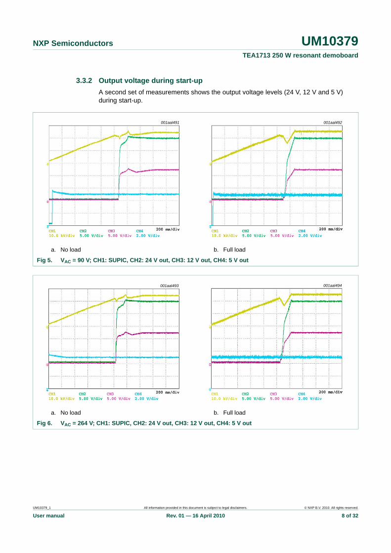
3.3.2 Output voltage during start-upA second set of measurements shows the output voltage levels (24 V, 12 V and 5 V) during start-up.
a. No load b. Full load
Fig 5. VAC = 90 V; CH1: SUPIC, CH2: 24 V out, CH3: 12 V out, CH4: 5 V out
001aal491 001aal492
a. No load b. Full load
Fig 6. VAC = 264 V; CH1: SUPIC, CH2: 24 V out, CH3: 12 V out, CH4: 5 V out
001aal493 001aal494
UM10379_1 All information provided in this document is subject to legal disclaimers. © NXP B.V. 2010. All rights reserved.
User manual Rev. 01 — 16 April 2010 8 of 32
NXP Semiconductors UM10379TEA1713 250 W resonant demoboard
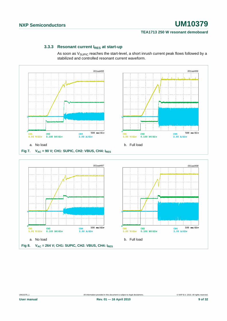
3.3.3 Resonant current IRES at start-upAs soon as VSUPIC reaches the start-level, a short inrush current peak flows followed by a stabilized and controlled resonant current waveform.
a. No load b. Full load
Fig 7. VAC = 90 V; CH1: SUPIC, CH2: VBUS, CH4: IRES
001aal495 001aal496
a. No load b. Full load
Fig 8. VAC = 264 V; CH1: SUPIC, CH2: VBUS, CH4: IRES
001aal497 001aal498
UM10379_1 All information provided in this document is subject to legal disclaimers. © NXP B.V. 2010. All rights reserved.
User manual Rev. 01 — 16 April 2010 9 of 32

NXP Semiconductors UM10379TEA1713 250 W resonant demoboard
3.3.4 IC supply voltages on pins SUPIC, SUPREG and SUPHVA high voltage must be present on pin SUPHV before the demo board can start up. SUPREG becomes operational as soon as SUPIC reaches the start-up voltage (typically 22 V). HBC and PFC operations are enabled when VSUPREG reaches 10.7 V.
a. No load b. Full load
Fig 9. VAC = 90 V; CH1: SUPIC, CH2: SUPREG, CH4: SUPHV
001aal499 001aal500
a. No load b. Full load
Fig 10. VAC = 264 V; CH1: SUPIC, CH2: SUPREG, CH4: SUPHV
001aal501 001aal502
UM10379_1 All information provided in this document is subject to legal disclaimers. © NXP B.V. 2010. All rights reserved.
User manual Rev. 01 — 16 April 2010 10 of 32

NXP Semiconductors UM10379TEA1713 250 W resonant demoboard
3.3.5 Protection levels on pins SNSCURHB and SNSOUT during start-upThe voltage levels on protection pins SNSCURHB and SNSOUT were measured during start-up. Safe start-up will follow provided a protection function has not been triggered (the TEA1713 will not start up if a protection function is active). The protection function is activated when VRCPROT reaches 4 V.
a. No load b. Full load
Fig 11. VAC = 90 V; CH1: RCPROT, CH2: SNSCURHB, CH3: SNSOUT, CH4: VBUS
001aal503 001aal504
a. No load b. Full load
Fig 12. VAC = 264 V; CH1: RCPROT, CH2: SNSCURHB, CH3: SNSOUT, CH4: VBUS
001aal505 001aal506
UM10379_1 All information provided in this document is subject to legal disclaimers. © NXP B.V. 2010. All rights reserved.
User manual Rev. 01 — 16 April 2010 11 of 32

NXP Semiconductors UM10379TEA1713 250 W resonant demoboard
3.4 EfficiencyInput and output power were measured at full load from low to high mains voltages. The efficiency was calculated after a 30 minute burn-in at 25 °C room temperature without a fan.
With Burst mode enabled, the efficiency for low/medium loads can be increased significantly. The following measurements were taken at 230 V (AC) with all outputs, except the 24 V output, unloaded.
Jumper J301 was removed to enable Burst mode.
In this example, the system enters Burst mode at approximately 3.5 W output power with the load decreasing. With the load increasing again, the system exits Burst mode at approximately 18 W output power. The burst comparator thresholds can be set individually.
Table 2. Efficiency resultsVAC supply Pi Po Efficiency90 V / 50 Hz 292.88 W 254.38 W 86.9 %
115 V / 50 Hz 285.23 W 254.2 W 89.1 %
180 V / 50 Hz 280.0 W 254.18 W 90.8 %
230 V / 50 Hz 278.4 W 254.26 W 91.3 %
264 V / 50 Hz 277.6 W 254.34 W 91.6 %
Fig 13. Efficiency measurement for low/medium loads at 230 V (AC) supply
Po (W)0 504020 3010
40
60
20
80
100
Normal mode
Burst modeEfficiency(%)
0
014aab005
UM10379_1 All information provided in this document is subject to legal disclaimers. © NXP B.V. 2010. All rights reserved.
User manual Rev. 01 — 16 April 2010 12 of 32

NXP Semiconductors UM10379TEA1713 250 W resonant demoboard
3.5 Transient responseThe dynamic load response of the 12 V and 24 V outputs was measured. The transient voltage should not show any ringing or oscillation.
Test results are given in Table 3.
Table 3. Transient response test resultsMeasurement conditions: 0 % to 100 % of full load; 200 ms duty cycle; 1 mA/μs rise/fall time
Output voltage Overshoot Undershoot Ringing12 V 230 mV 250 mV free
24 V 145 mV 165 mV free
a. 12 V (0 A to 4 A); 24 V loaded with 8 A b. 24 V (0 A to 8 A); 12 V loaded with 4 A
Fig 14. Transient response
001aal507 001aal508
UM10379_1 All information provided in this document is subject to legal disclaimers. © NXP B.V. 2010. All rights reserved.
User manual Rev. 01 — 16 April 2010 13 of 32

NXP Semiconductors UM10379TEA1713 250 W resonant demoboard
3.6 Output ripple and noiseRipple and noise were measured at full output load, buffered with a 10 μF capacitor in parallel with a high-frequency 0.1 μF capacitor.
Table 4. Ripple and noise test resultsVAC supply VO Load Ripple and noise90 V to 264 V / 50 Hz 24 V 8 A 40 mV (p-p)
12 V 4 A 25 mV (p-p)
a. VAC = 90 V b. VAC = 264 V
Fig 15. Ripple and noise; CH1: 24 V out, CH2: 12 V out
001aal509 001aal510
UM10379_1 All information provided in this document is subject to legal disclaimers. © NXP B.V. 2010. All rights reserved.
User manual Rev. 01 — 16 April 2010 14 of 32

NXP Semiconductors UM10379TEA1713 250 W resonant demoboard
3.7 OverPower Protection (OPP)These measurements were taken to determine the output power level at which the system initiates a soft start.
Setup: constant load currents at output 2 (12 V / 4 A) and output 3 (5 V / 2 A); the load current at output 1 (24 V output) is gradually increased to determine the OPP trip point.
The protection timer starts (and the TEA1713 increases the switching frequency) once the voltage on pin SNSCURHBC rises above +0.5 V and/or falls below −0.5 V. As soon as VSNSCURHBC falls below +0.5 V again and/or rises above −0.5 V, the protection timer stops. Thus the maximum primary current remains constant (at the OPP level) whereas the output voltage decreases with frequency.
If increasing the frequency fails to restrict VSNSCURHBC to between +0.5 V and −0.5 V, the protection timer will continue counting until eventually triggering a safe system restart.
The measurements show that, when the load increases to around 315 W, the system tries continuously to restart (for VAC = 115 V, 180 V, 230 V and 264 V). This corresponds to a power rating of 126 %. See Figure 16
Table 5. Test results for VAC = 90 V and nominal output power of 254 WI (output 1) V (output 1) I (output 2) V (output 2) Power output
(total)Rating
9.25 A 24 V 4 A 12 V 280 W 110.2 %
9.52 A 23.7 V 4 A 11.7 V 282.4 W 111.2 %
10 A 22.4 V 4 A 11.4 V 279.6 W 110.1 %
10.5 A 21.5 V 4 A 10.6 V 278.15 W 109.5 %
a. CH1: SUPIC, CH2: SNSCURHB,CH3: RCPROT, CH4: SNSOUT
b. CH1: SUPIC, CH2: 24 V out,CH3: RCPROT, CH4: SNSOUT
Fig 16. Overpower protection
001aal511 001aal512
UM10379_1 All information provided in this document is subject to legal disclaimers. © NXP B.V. 2010. All rights reserved.
User manual Rev. 01 — 16 April 2010 15 of 32
NXP Semiconductors UM10379TEA1713 250 W resonant demoboard
From Figure 16 a, we can see that OPP is triggered initially when VRCPROT reaches 4 V for the first time (because VSNSCURHB fails to fall below +0.5 V and/or rise above −0.5 V even though the controller increased the switching frequency in an attempt to limit the voltage swing to between +0.5 V and −0.5 V).
As soon as VRCPROT reaches the protection threshold of 4 V, the IC initiates a soft start. The second and third times RCPROT is activated is caused by heavy load condition (see CH2 in Figure 16 b). The voltage at the SNSOUT pin was unable to rise above its UVLO range. The fourth time, RCPROT is triggered by UVLO on the SUPIC pin. Due to the low output voltage, the auxiliary winding could not deliver sufficient energy to the SUPIC pin. The UVLO on SUPIC forces the converter to restart even though RCPROT has not reached 4 V.
Figure 16 a and b illustrate clearly how OPP can be triggered by a number of protection mechanisms. In this example it is triggered by SNSCURHB and SNSOUT, as well as by SUPIC.
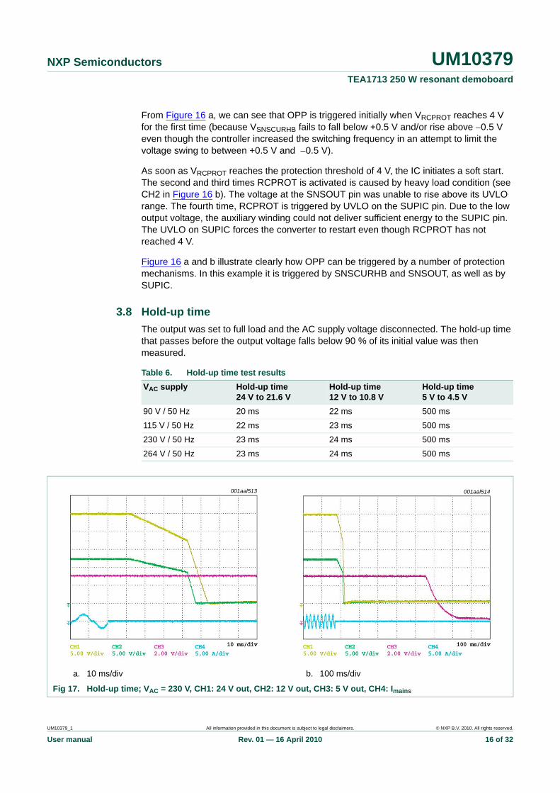
3.8 Hold-up timeThe output was set to full load and the AC supply voltage disconnected. The hold-up time that passes before the output voltage falls below 90 % of its initial value was then measured.
Table 6. Hold-up time test resultsVAC supply Hold-up time
24 V to 21.6 VHold-up time 12 V to 10.8 V
Hold-up time 5 V to 4.5 V
90 V / 50 Hz 20 ms 22 ms 500 ms
115 V / 50 Hz 22 ms 23 ms 500 ms
230 V / 50 Hz 23 ms 24 ms 500 ms
264 V / 50 Hz 23 ms 24 ms 500 ms
a. 10 ms/div b. 100 ms/div
Fig 17. Hold-up time; VAC = 230 V, CH1: 24 V out, CH2: 12 V out, CH3: 5 V out, CH4: Imains
001aal513 001aal514
UM10379_1 All information provided in this document is subject to legal disclaimers. © NXP B.V. 2010. All rights reserved.
User manual Rev. 01 — 16 April 2010 16 of 32

NXP Semiconductors UM10379TEA1713 250 W resonant demoboard
3.9 Short Circuit Protection (SCP)If the power supply outputs are shorted under no load or full load conditions, a safe system restart will be initiated.
From Figure 18 a, we can see that SCP is triggered initially when VRCPROT reaches 4 V for the first time because VSNSCURHB fails to fall below ± 0.5 V, even though the controller increased the switching frequency in an attempt to lower this voltage.
Subsequently, SCP is triggered by heavy load condition. Since the 24 V rail is shorted, the voltage across the auxiliary winding also falls. The second peak of VRCPROT is below 4 V (it initiates a soft restart at 4 V) when SUPIC reaches its UVLO threshold. The third and fourth peaks of VSNSCURHB reach 4 V due to UVLO on pin SNSOUT or on pin SUPIC. SCP mechanisms are basically the same as OPP mechanisms.
a. VAC = 90 V b. VAC = 264 V
Fig 18. CH1: SUPIC, CH2: GATEPFC, CH3: RCPROT, CH4: SNSOUT
001aal515 001aal516
UM10379_1 All information provided in this document is subject to legal disclaimers. © NXP B.V. 2010. All rights reserved.
User manual Rev. 01 — 16 April 2010 17 of 32

NXP Semiconductors UM10379TEA1713 250 W resonant demoboard
3.10 Resonant current measurementThe gate drive signals and resonant current at no load and at full load were measured. The converter operates in Zero Voltage Switching (ZVS) mode.
3.11 Cross regulationVoltage regulation can be measured at 24 V / 8 A and 12 V / 0 A or at 24 V / 0 A and 12 V / 4 A, with J301 inserted to inhibit possible Burst mode intervention.
a. No load b. Full load
Fig 19. Resonant current test results; CH1: GATELS, CH4: IRES
001aal517 001aal518
Table 7. Cross regulation test resultsLoad conditions 24 V 12 V
Measure Regulation Measure Regulation24 V / 8 A12 V / 0 A
24.31 V 1.3 % 12.61 V 5.1 %
24 V / 0 A12 V / 4 A
25.0 V 4.2 % 11.63 V 3.1 %
UM10379_1 All information provided in this document is subject to legal disclaimers. © NXP B.V. 2010. All rights reserved.
User manual Rev. 01 — 16 April 2010 18 of 32

xxxxxxxxxxxxxxxxxxxxx xxxxxxxxxxxxxxxxxxxxxxxxxx xxxxxxx x x x xxxxxxxxxxxxxxxxxxxxxxxxxxxxxx xxxxxxxxxxxxxxxxxxx xx xx xxxxx xxxxxxxxxxxxxxxxxxxxxxxxxxx xxxxxxxxxxxxxxxxxxx xxxxxx xxxxxxxxxxxxxxxxxxxxxxxxxxxxxxxxxxx xxxxxxxxxxxx x x xxxxxxxxxxxxxxxxxxxxx xxxxxxxxxxxxxxxxxxxxxxxxxxxxxx xxxxx xxxxxxxxxxxxxxxxxxxxxxxxxxxxxxxxxxxxxxxxxxxxxxxxxx xxxxxxxx xxxxxxxxxxxxxxxxxxxxxxxxx xxxxxxxxxxxxxxxxxxxx xxx
UM
10379_1
User m
anual
NXP Sem
iconductorsU
M10379
TEA1713 250 W
resonant demoboard
4. Board properties
4.1 Circuit diagram
1900 μF
C3141 mF
L3010.9 μH
C3151 mF
C3161 mF
C3171 mF
C3201000 μF
L3020.9 μH
R31236 kΩ
R31768 Ω
0
.
R31410 kΩ
R3232.7 kΩ
C32347 nF
R313910 Ω
R315470 Ω
R31882 Ω
IC303TL431
C3252.2 nF
C324n.m.
24 V 8 A
12 V 4 A
014aab003
All information provided in this docum
ent is subject to legal disclaimers.
© N
XP B.V. 2010. All rights reserved.
Rev. 01 —
16 April 2010
19 of 32
Fig 20. Half bridge resonant converter stage
TEA1713
IC101
SUPREG
6
5
7
28
4 3
1
IC102BLM393
C3222 μF
C311n.m.
C305330 pF
C3263.3 μF
R302150 kΩ
R30327 kΩ
1311
14
15
16
17
18
19
20
RCPROT
SSHBC/EN
SNSFB
RFMAX
CFMIN
SGND
n.c.
n.c.
HB
SUPHS
D3121N4007
D3511N4148
C312330 nF
C308680 nF
C3004.7 μF
C306680 nF
C32110 nF
C365390 nF
C304220 μF
C30710 μF
C3091 nF
C3182.7 nF
C310
C3131 mF
C31047 nF
D303SBL2060CT
D304SBL2060CT
D305SBL2040CT
D306SBL2040CT
T1LP3925
R3011 kΩ
R35110 Ω
R353100 kΩ
R36639 kΩ
R357100 kΩ
R35651 Ω
D3551N4148
C301220 pF
C302220 pF
Q30112N50C3
Q30212N50C3
R35510 Ω
R35251 Ω
R1170 Ω
R3672.2 kΩ
R36233 kΩ
R363100 kΩ
Q307BC847-40 C362
3.3 nF
C36110 nF
C360150 nF
R370 Ωn.m
R3710 Ω
R364n.m.
IC302SFH615
IC102ALM393
R36912 kΩ
R3680 Ω
R36033 kΩ
R36165 kΩ J301
PGNDSGND
R365270 kΩ
R12375 Ω
R3107.5 Ω
D3661N4148
D3561N4148
GATEHS
GATELS
VBUS
SUPREGSUPREG
SNSCURHB
SUPREG
SUPREG
AUX windingadded by hand
SUPIC
SUPIC
SNSOUT
SNSCURHB
SUPREG
SNSCURHB
EN
21
22
23
10
9
6
5
Remove J301 toenable burst mode
R380n.m.

xxxxxxxxxxxxxxxxxxxxx xxxxxxxxxxxxxxxxxxxxxxxxxx xxxxxxx x x x xxxxxxxxxxxxxxxxxxxxxxxxxxxxxx xxxxxxxxxxxxxxxxxxx xx xx xxxxx xxxxxxxxxxxxxxxxxxxxxxxxxxx xxxxxxxxxxxxxxxxxxx xxxxxx xxxxxxxxxxxxxxxxxxxxxxxxxxxxxxxxxxx xxxxxxxxxxxx x x xxxxxxxxxxxxxxxxxxxxx xxxxxxxxxxxxxxxxxxxxxxxxxxxxxx xxxxx xxxxxxxxxxxxxxxxxxxxxxxxxxxxxxxxxxxxxxxxxxxxxxxxxx xxxxxxxx xxxxxxxxxxxxxxxxxxxxxxxxx xxxxxxxxxxxxxxxxxxxx xxx
UM
10379_1
User m
anual
NXP Sem
iconductorsU
M10379
TEA1713 250 W
resonant demoboard
L
C110220 μF420 V
C10910 nF
C102 D101 D102BYV29X-600
VBUS
L104
BD101GBU806
FUSE F101R1021 MΩ
R122
R20.1 Ω1 W
100 kΩ
Q101K3934 R112
4.7 MΩ
R1134.7 MΩ
R11456 kΩ
R1202.2 kΩ
R10.1 Ω
1 W
IC304SFH610
R32091 Ω
R3000 Ω
S1STBYEN
+ 5 V
D320nc
D321nc
014aab004
All information provided in this docum
ent is subject to legal disclaimers.
© N
XP B.V. 2010. All rights reserved.
Rev. 01 —
16 April 2010
20 of 32
Fig 21. PFC stage (top circuit) and stand-by supply (bottom circuit)
G
N
1
2
3
4
8
7
6
5
n.c.
DRAIN
24SNSBOOST
4SNSCURPFC
7GATEPFC
12SUPHV
3SNSAUXPFC
2
8
SNSMAINS
PGND
1COMPPFC
C105150 nF
C106470 nF
C1133.3 μF
C1121 μF
C1110.22 μF
C1030.22 μF
2.2 nFL101 L102
C1012.2 nF C114
1 μF
R10833 kΩ
R1093.6 kΩ
R1035.1 kΩ
L103L ≅ 220 μH 1N5408
VBUS
220 μH
R116560 kΩ
CN101
R10447 kΩ
R1190 Ω
1 MΩ
R1211 MΩ
R1011 MΩ
TEA1522
IC201
SOURCE
AUX
GND
RC
REG
C20610 nF
C4013.3 nFR206
5.1 kΩ
R2171 Ω
R20475 kΩR237
12 kΩC215220 pF
C20222 μF
C2012.2 nF
D2011N4007
T201
D2021N4148
R2034.7 Ω
R201470 kΩ
R118n.c.
R216n.c. R218
10 kΩ
R21910 kΩ
R2151.5 kΩ
R208100 Ω
R1152.2 kΩ
PBSSR10712 kΩ
C10747 nF
R110Q201
5350T
R11110 Ω
C2081.5 nF
C211470 μF
C210470 μF
D20448CTQ060
C209470 μF
5V 2A
R2135.1 kΩ
IC203TL431
IC202SFH615
C21347 nF
C21222 nF
VBUS
VCC
VCC
VCC
SUPIC
ZD20130 V
TEA1713
IC101 (PART)
L2010.9 μHR200
0 Ω

NXP Semiconductors UM10379TEA1713 250 W resonant demoboard
4.2 PCB layout
4.3 Bill of Materials
Fig 22. PCB layout of TEA1713 250 W demo board
014aab006
Table 8. Bill of materialPart
PFCBD101 Bridge diode, flat/mini, GBU806 8 A, 600 V (Lite-On)
C101 Ceramic disc capacitor, Y2-type, 9 ϕ, KX 2200 pF, 250 V (AC) (Murata):
C102 Ceramic disc capacitor, Y2-type, 9 ϕ, KX 2200 pF, 250 V (AC) (Murata):
C103 MPX, X-Cap 0.22 μF, 275 V (AC)
C105 MLCC, SMD 0805, X7R 150 nF, 50 V
C106 MLCC, SMD 0805, X7R 470 nF, 50 V
C107 MLCC, SMD 0805, X7R 47 nF, 50 V
C109 MLCC, SMD 0805, X7R 10 nF, 50 V
C110 E/C, Radial Lead, 85°C, 220 μF, 420 V
UM10379_1 All information provided in this document is subject to legal disclaimers. © NXP B.V. 2010. All rights reserved.
User manual Rev. 01 — 16 April 2010 21 of 32

NXP Semiconductors UM10379TEA1713 250 W resonant demoboard
C111 MPX, X-Cap 0.22 μF, 275 V (AC)
C112 MPP Cap. Radial Lead 1 μF, 450 V
C113 MLCC, SMD 0805, 3300 nF, 25 V
C114 MPP Cap. Radial lead 1 μF, 450 V
D101 General purpose diode, 1N5408 3 A, 1 KV
D102 BYV29X-600 TO220 F-pack
F101 Fuse, / PTU 6.3 A, 250 V
IC101 TEA1713 SO24 (NXP)
L101 EMI Choke, Ring core, 18 mm, / 2.0 mH (Sendpower)
L102 EMI Choke, FOTC2508000900A, 9.0 mH (Yu Jing International)
L103 PFC Choke, QP-3325 220 μH with auxiliary winding (Yu Jing International)
L104 Power Choke 220 μH (Yu Jing International)
Q101 MOSFET K3934 TO220 F-pack
Q201 PNP PBSS5350T
R1 Resistor, axial lead, 1 W, small size 0.1 Ω, 5 %
R2 Resistor, axial lead, 1 W, small size 0.1 Ω, 5 %
R101 Resistor, SMD 1206 thin film chip 1 MΩ, 5 %
R102 Resistor, SMD 1206 thin film chip 1 MΩ, 5 %
R103 Resistor, SMD 0805 thin film chip 5.1 kΩ, 5 %
R104 Resistor, SMD 0805 thin film chip 47 kΩ, 5 %
R107 Resistor, SMD 0805 thin film chip 12 kΩ, 5 %
R108 Resistor, SMD 0805 thin film chip 33 kΩ, 5 %
R109 Resistor, SMD 0805 thin film chip 3.6 kΩ, 5 %
R110 Resistor, SMD 0805 thin film chip 100 kΩ, 5 %
R111 Resistor, SMD 1206 thin film chip 10 Ω, 5 %
R112 Resistor, SMD 1206 thin film chip 4.7 MΩ, 5 %
R113 Resistor, SMD 1206 thin film chip 4.7 MΩ, 5 %
R114 Resistor, SMD 0805 thin film chip 56 kΩ, 1 %
R115 Resistor, SMD 0805 thin film chip 2.2 kΩ, 5 %
R116 Resistor, SMD 0805 thin film chip 560 kΩ, 5 %
R119 Resistor, SMD 0805 thin film chip 0 Ω, 5 %
R120 Resistor, SMD 0805 thin film chip 2.2 kΩ, 5 %
R121 Resistor, SMD 1206 thin film chip 1 MΩ, 5 %
R122 Resistor, SMD 1206 thin film chip 1 MΩ, 5 %
Resonant LLC converter stageC300 E/C, Radial Lead, 4.7 μF / 16 V
C301 Ceramic capacitor, Disc, 5ϕ 220 pF, 1 kV
C302 Ceramic capacitor, Disc, 5ϕ 220 pF, 1 kV
C304 E/C, Radial Lead, 7.5 mm × 12 mm, 220 μF / 35 V
C305 MLCC, SMD 0805, X7R 330 pF, 50 V
C306 MLCC, SMD 0805, X7R 680 nF, 50 V
Table 8. Bill of material …continued
Part
UM10379_1 All information provided in this document is subject to legal disclaimers. © NXP B.V. 2010. All rights reserved.
User manual Rev. 01 — 16 April 2010 22 of 32

NXP Semiconductors UM10379TEA1713 250 W resonant demoboard
C307 E/C, radial lead, 7.5 mm × 12 mm, 10 μF / 35 V
C308 MLCC, SMD 0805, X7R 680 nF, 50 V
C309 Ceramic disc capacitor, 5ϕ 1000 pF, 1 KV
C310 MPP radial lead capacitor, high current 47 nF, 800 V or 1000 V
C311 n.m. (not mounted)
C312 MLCC, SMD 0805, X7R 330 nF, 50 V
C313 E/C radial lead capacitor, 12.5 mm × 20 mm, 1000 μF / 35 V
C314 E/C radial lead capacitor, 12.5 mm × 20 mm, 1000 μF / 35 V
C315 E/C radial lead capacitor, 12.5 mm × 20 mm, 1000 μF / 35 V
C316 E/C radial lead capacitor, 12.5 mm × 20 mm, 1000 μF / 35 V
C317 E/C radial lead capacitor, 12.5 mm × 20 mm, 1000 μF / 35 V
C318 MLCC, SMD 0805, X7R 2.7 nF, 50 V
C319 E/C radial lead capacitor, 10 mm × 15 mm, 1000 μF / 16 V
C320 E/C radial lead capacitor, 10 mm × 15 mm, 1000 μF / 16 V
C321 MLCC, SMD 0805, X7R 10 nF, 50 V
C322 MLCC, SMD 0805, 2.2 μF, 16 V
C323 MLCC, SMD 0805, X7R 47 nF, 50 V
C324 n.m. (not mounted)
C325 MLCC, SMD 0805, X7R 2.2 nF, 50 V
C326 MLCC, SMD 0805, 3.3 μF, 16 V
C360 MLCC, SMD 0805, X7R 150 nF, 50 V
C361 MLCC, SMD 0805, X7R 10 nF, 50 V
C362 MLCC, SMD 0805, X7R 3.3 nF, 50 V
C365 MLCC, SMD 0805, X7R 390 nF, 50 V
D303 Schottky diode, TO220AB, SBL2060CT, 20 A, 60 V (Lite-On)
D304 Schottky diode, TO220AB, SBL2060CT, 20 A, 60 V (Lite-On)
D305 Schottky diode, TO220AB, SBL2040CT, 20 A, 40 V (Lite-On)
D306 Schottky diode, TO220AB, SBL2040CT, 20 A, 40 V (Lite-On)
D312 General purpose diode, 1N4007 1 A, 1 KV or alternatively fast recovery diode UF4007
D351 Switching diode, SMD SOD-80, LL4148, 0.2 A, 75 V (NXP)
D355 Switching diode, SMD SOD-80, LL4148, 0.2 A, 75 V(NXP)
D356 Switching diode, SMD SOD-80, LL4148, 0.2 A, 75 V (NXP)
D366 Switching diode, SMD SOD-80, LL4148, 0.2 A, 75 V (NXP)
IC102 LM393 SO8
IC302 Optocoupler, SFH615A-1
IC303 Voltage regulator, TO92, TL431
J301 Jumper
L301 Power choke; 0.9 μH (Sendpower)core: R4 × 15; wiring: 1.2 mm (diameter) × 6.5 turns
L302 Power choke; 0.9 μH (Sendpower)core: R4 × 15; 1.2 mm (diameter) × 6.5 turns
Table 8. Bill of material …continued
Part
UM10379_1 All information provided in this document is subject to legal disclaimers. © NXP B.V. 2010. All rights reserved.
User manual Rev. 01 — 16 April 2010 23 of 32

NXP Semiconductors UM10379TEA1713 250 W resonant demoboard
Q301 NMOS SPA12N50C3 TO220
Q302 NMOS SPA12N50C3 TO220
Q307 BC847
R117 Resistor, SMD 0805 thin film chip 0 Ω
R123 Resistor, SMD 0805 thin film chip 75 Ω, 5 %
R301 Resistor, SMD 0805 thin film chip 1 kΩ, 5 %
R302 Resistor, SMD 0805 thin film chip 150 kΩ, 5 %
R303 Resistor, SMD 0805 thin film chip 27 kΩ, 5 %
R310 Resistor, SMD 0805 thin film chip 7.5 Ω, 5 %
R312 Resistor, SMD 0805 thin film chip 36 kΩ, 1 %
R313 Resistor, SMD 0805 thin film chip 910 Ω, 1 %
R314 Resistor, axial lead 1/4 W 10 kΩ, 1 %
R315 Resistor, axial lead 1/4 W 470 Ω, 1 %
R317 Resistor, SMD 0805 thin film chip 68 Ω, 5 %
R318 Resistor, SMD 0805 thin film chip 82 Ω, 5 %
R323 Resistor, SMD 0805 thin film chip 2.7 kΩ, 5 %
R351 Resistor, SMD 0805 thin film chip 10 Ω, 5 %
R352 Resistor, SMD 0805 thin film chip 51 Ω, 5 %
R353 Resistor, SMD 0805 thin film chip 100 kΩ, 5 %
R355 Resistor, SMD 0805 thin film chip 10 Ω, 5 %
R356 Resistor, SMD 0805 thin film chip 51 Ω, 5 %
R357 Resistor, SMD 0805 thin film chip 100 k Ω, 5 %
R360 Resistor, SMD 1206 thin film chip 33 kΩ, 1 %
R361 Resistor, SMD 0805 thin film chip 65 kΩ, 1 %; if burst problems: check similar values (e.g. values between 56 kΩ and 68 kΩ)
R362 Resistor, SMD 1206 thin film chip 33 kΩ, 5 %
R363 Resistor, SMD 1206 thin film chip 100 kΩ, 5 %
R364 n.m. (not mounted)
R365 Resistor, SMD 0805 thin film chip 270 kΩ, 5 %
R366 Resistor, SMD 0805 thin film chip 39 kΩ, 5 %
R367 Resistor, SMD 0805 thin film chip 2.2 kΩ, 5 %
R368 Resistor, SMD 0805 thin film chip 0 Ω, 5 %
R369 Resistor, SMD 0805 thin film chip 12 kΩ, 5 %
R370 n.m. (not mounted)
R371 Resistor, SMD 0805 thin film chip 0 Ω, 5 %
R380 n.m. (not mounted)
T1 Transformer, LP3925, Lk = 110 μH, L = 660 μH (Yu Jing International)add 4 auxiliary windings
Flyback stageC201 Ceramic disc capacitor, 5ϕ 2200 pF, 1 kV
C202 E/C radial lead capacitor, 105 °C, 6.3 mm × 11 mm, LZP 22 μF, 50 V (LTEC)
Table 8. Bill of material …continued
Part
UM10379_1 All information provided in this document is subject to legal disclaimers. © NXP B.V. 2010. All rights reserved.
User manual Rev. 01 — 16 April 2010 24 of 32

NXP Semiconductors UM10379TEA1713 250 W resonant demoboard
C206 MLCC, SMD 0805, X7R 10 nF, 50 V
C208 MLCC, SMD 0805, X7R 1.5 nF, 50 V
C209 E/C radial lead capacitor,105 °C, 5 mm × 12 mm, LZP 470 μF, 16 V (LTEC)
C210 E/C radial lead capacitor, 5 mm × 12 mm, LZP 470 μF, 16 V (LTEC)
C211 E/C radial lead capacitor, 105°C, 5 mm × 12 mm, LZP 470 μF, 16 V (LTEC)
C212 MLCC, SMD 0805, X7R 22 nF, 50 V
C213 MLCC, SMD 0805, X7R 47 nF, 50 V
C215 MLCC, SMD 0805, X7R 220 pF, 50 V
C401 Ceramic, Y1-Cap, Disc 9ϕ, KX 3300 pF, 250 V (AC) (Murata)
D201 General purpose diode, 1N4007 1 A, 1 KV
D202 Switching diode, DIP, 1N4148, 0.2 A, 75 V (NXP)
D204 Schottky diode, TO220AB, SBL1040CT, 10 A, 40 V (Lite-On)
D320 n.m. (not mounted)
D321 n.m. (not mounted)
IC201 SMPS controller IC, SO8, TEA1522P (NXP)
IC202 Optocoupler, SFH615A-1
IC203 Voltage regulator, TO92, TL431
IC304 Optocoupler, SFH610A-1
L201 Power choke; 0.9 μH (Sendpower)core: R4 × 15; wiring: 1.2 mm (diameter) × 6.5 turns
R118 n.m. (not mounted)
R200 Resistor, SMD 1206 thin film chip 0 Ω,
R201 Resistor, axial lead, CF 1/4 W, small size 470 kΩ, 5 %
R203 Resistor, SMD 0805 thin film chip 4.7 Ω, 5 %
R204 Resistor, axial lead 1/4 W 75 kΩ, 5 %
R206 Resistor, SMD 0805 thin film chip 5.1 kΩ, 5 %
R208 Resistor, SMD 0805 thin film chip 100 Ω, 5 %
R213 Resistor, SMD 0805 thin film chip 5.1 kΩ, 5 %
R215 Resistor, SMD 0805 thin film chip 1.5 kΩ, 5 %
R216 n.m. (not mounted)
R217 Resistor, axial lead 1/4W 1 Ω, 5 %
R218 Resistor, SMD 0805 thin film chip 10 kΩ, 1 %
R219 Resistor, SMD 0805 thin film chip 10 kΩ, 1 %
R237 Resistor, SMD 0805 thin film chip 12 kΩ, 5 %
R300 Resistor, SMD 0805 thin film chip 0 Ω, 5 %
R320 Resistor, SMD 0805 thin film chip 91 Ω, 5 %
S1 Switch, small signal, 6 pin
T201 Transformer, EF20 PC40 2.1 mH (TDK)
ZD201 Zener diode, SMD BZX84-C30, 30 V (NXP)
Table 8. Bill of material …continued
Part
UM10379_1 All information provided in this document is subject to legal disclaimers. © NXP B.V. 2010. All rights reserved.
User manual Rev. 01 — 16 April 2010 25 of 32
NXP Semiconductors UM10379TEA1713 250 W resonant demoboard
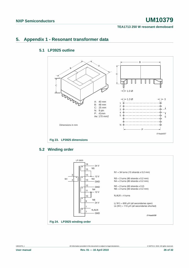
5. Appendix 1 - Resonant transformer data
5.1 LP3925 outline
5.2 Winding order
Fig 23. LP3925 dimensions
A: 40 mm
B: 48 mm
C: 25 mm
N: 8 pin
P: 41mm
Ae: 170 mm2
Dimensions in mm
P
B
C
5
1.3 Ø
1.0 Ø
AB
C
1
2
3
4
5
N
3
014aab007
Fig 24. LP3925 winding order
LP-3925
N1 = 34 turns (15 strands x 0.2 mm)
N3 = 2 turns (80 strands x 0.2 mm)N4 = 2 turns (80 strands x 0.2 mm)
N5 = 2 turns (60 strands x 0.2)N6 = 2 turns (60 strands x 0.2 mm)
L( N1) = 600 μH (all secondaries open)Lk (N1) = 110 μH (all secondaries shorted)
N,AUX = 4 turns
24 V16
15
14
13N1
N5
N3
N4
N6
N,AUX
4
3
12
11
10
9
1
7
12 V
GND
GND
12 V
24 V
GND014aab008
UM10379_1 All information provided in this document is subject to legal disclaimers. © NXP B.V. 2010. All rights reserved.
User manual Rev. 01 — 16 April 2010 26 of 32

NXP Semiconductors UM10379TEA1713 250 W resonant demoboard
6. Appendix 2 - PFC transformer data
6.1 QP-3325 outline
6.2 Winding order
Fig 25. QP-3325 dimensions
BOTTOM VIEW
C67 C23
P2
Ae: 200 mm2
P1
A
P2P1
8
7
6
5 4
3
2
1
B
C
A: 37 mm (max)B: 26 mm (max)C: 34.5 mm (max)
P1: 24 ±0.5 mmP2: 30 ±0.5 mm
014aab009
Fig 26. QP-3325 winding order
7,8N2
QP-3325
N13,4
1,2
6,5
Lp (N1) = 220 μH (for N2 Open)N1 = 50 Ts (70 strands x 0.1 mm)N2 = 3.5 Ts (1 strand x 0.3 mm)
014aab010
UM10379_1 All information provided in this document is subject to legal disclaimers. © NXP B.V. 2010. All rights reserved.
User manual Rev. 01 — 16 April 2010 27 of 32
NXP Semiconductors UM10379TEA1713 250 W resonant demoboard
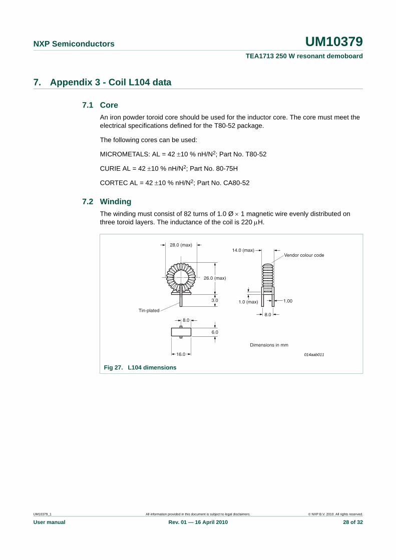
7. Appendix 3 - Coil L104 data
7.1 CoreAn iron powder toroid core should be used for the inductor core. The core must meet the electrical specifications defined for the T80-52 package.
The following cores can be used:
MICROMETALS: AL = 42 ±10 % nH/N2; Part No. T80-52
CURIE AL = 42 ±10 % nH/N2; Part No. 80-75H
CORTEC AL = 42 ±10 % nH/N2; Part No. CA80-52
7.2 WindingThe winding must consist of 82 turns of 1.0 Ø × 1 magnetic wire evenly distributed on three toroid layers. The inductance of the coil is 220 μH.
Fig 27. L104 dimensions
Tin-plated
28.0 (max)
26.0 (max)
3.0
8.0
16.0
6.0
8.0
1.0 (max) 1.00
14.0 (max)Vendor colour code
Dimensions in mm
014aab011
UM10379_1 All information provided in this document is subject to legal disclaimers. © NXP B.V. 2010. All rights reserved.
User manual Rev. 01 — 16 April 2010 28 of 32

NXP Semiconductors UM10379TEA1713 250 W resonant demoboard
8. Appendix 4 - Standby transformer data
8.1 EF20 transformer with TDK PC40 core
8.2 Winding specifications
8.3 Electrical characteristics
8.4 Core and bobbinCore: EF-20 (TDK PC40 or equivalent)
Bobbin: EF-20 (6-pin vertical type, Chang Chun Plastics Co. Ltd)
Ae: 32.1 mm2
Fig 28. Winding order
N2
N5
N4
N3
N2
N1
Bobbin
S5
S4
S3
S2
S1
N43
6
5
BN3
AN1
2
N51
T
014aab012
Table 9. Winding specificationsLayer Winding Wire Turns Winding
MethodTape insulation
Start Finish No. Turns WidthN1 2 A 0.25 Ø × 1 40 center S1 2 13 mm
N2 6 5 0.35 Ø × 4 (3L) 5 center S2 2 13 mm
N3 A B 0.25 Ø × 1 40 center S3 1 13 mm
N4 B 3 0.25 Ø × 1 40 center S4 2 13 mm
N5 1 1 0.3 Ø × 1 20 side S5 3 13 mm
Table 10. Electrical characteristicsItem Pin Specification ConditionInductance 2 to 3 2.1 mH ±5% 80 kHz, 1 V
Leakage inductance 2 to 3 <100 μH 2nd all short
UM10379_1 All information provided in this document is subject to legal disclaimers. © NXP B.V. 2010. All rights reserved.
User manual Rev. 01 — 16 April 2010 29 of 32
NXP Semiconductors UM10379TEA1713 250 W resonant demoboard
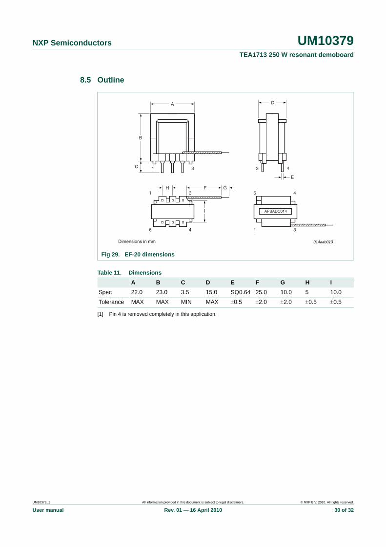
8.5 Outline
[1] Pin 4 is removed completely in this application.
Fig 29. EF-20 dimensions
Table 11. DimensionsA B C D E F G H I
Spec 22.0 23.0 3.5 15.0 SQ0.64 25.0 10.0 5 10.0
Tolerance MAX MAX MIN MAX ±0.5 ±2.0 ±2.0 ±0.5 ±0.5
Dimensions in mm
A
H F G
D
E
B
C 1 3 3 4
6 4
1 3
1 3
6 4
I APBADC014
014aab013
UM10379_1 All information provided in this document is subject to legal disclaimers. © NXP B.V. 2010. All rights reserved.
User manual Rev. 01 — 16 April 2010 30 of 32
NXP Semiconductors UM10379TEA1713 250 W resonant demoboard
9. Legal information
9.1 DefinitionsDraft — The document is a draft version only. The content is still under internal review and subject to formal approval, which may result in modifications or additions. NXP Semiconductors does not give any representations or warranties as to the accuracy or completeness of information included herein and shall have no liability for the consequences of use of such information.
9.2 DisclaimersLimited warranty and liability — Information in this document is believed to be accurate and reliable. However, NXP Semiconductors does not give any representations or warranties, expressed or implied, as to the accuracy or completeness of such information and shall have no liability for the consequences of use of such information.
In no event shall NXP Semiconductors be liable for any indirect, incidental, punitive, special or consequential damages (including - without limitation - lost profits, lost savings, business interruption, costs related to the removal or replacement of any products or rework charges) whether or not such damages are based on tort (including negligence), warranty, breach of contract or any other legal theory.
Notwithstanding any damages that customer might incur for any reason whatsoever, NXP Semiconductors’ aggregate and cumulative liability towards customer for the products described herein shall be limited in accordance with the Terms and conditions of commercial sale of NXP Semiconductors.
Right to make changes — NXP Semiconductors reserves the right to make changes to information published in this document, including without limitation specifications and product descriptions, at any time and without notice. This document supersedes and replaces all information supplied prior to the publication hereof.
Suitability for use — NXP Semiconductors products are not designed, authorized or warranted to be suitable for use in medical, military, aircraft, space or life support equipment, nor in applications where failure or malfunction of an NXP Semiconductors product can reasonably be expected to result in personal injury, death or severe property or environmental damage. NXP Semiconductors accepts no liability for inclusion and/or use of NXP Semiconductors products in such equipment or applications and therefore such inclusion and/or use is at the customer’s own risk.
Applications — Applications that are described herein for any of these products are for illustrative purposes only. NXP Semiconductors makes no representation or warranty that such applications will be suitable for the specified use without further testing or modification.
NXP Semiconductors does not accept any liability related to any default, damage, costs or problem which is based on a weakness or default in the customer application/use or the application/use of customer’s third party customer(s) (hereinafter both referred to as “Application”). It is customer’s sole responsibility to check whether the NXP Semiconductors product is suitable and fit for the Application planned. Customer has to do all necessary testing for the Application in order to avoid a default of the Application and the product. NXP Semiconductors does not accept any liability in this respect.
Export control — This document as well as the item(s) described herein may be subject to export control regulations. Export might require a prior authorization from national authorities.
9.3 TrademarksNotice: All referenced brands, product names, service names and trademarks are the property of their respective owners.
UM10379_1 All information provided in this document is subject to legal disclaimers. © NXP B.V. 2010. All rights reserved.
User manual Rev. 01 — 16 April 2010 31 of 32

NXP Semiconductors UM10379TEA1713 250 W resonant demoboard
10. Contents
1 Introduction . . . . . . . . . . . . . . . . . . . . . . . . . . . . 32 Setup. . . . . . . . . . . . . . . . . . . . . . . . . . . . . . . . . . 32.1 Normal operation . . . . . . . . . . . . . . . . . . . . . . . 32.2 Burst mode operation . . . . . . . . . . . . . . . . . . . . 43 Measurements . . . . . . . . . . . . . . . . . . . . . . . . . . 53.1 Test facilities . . . . . . . . . . . . . . . . . . . . . . . . . . . 53.2 Standby power/no load power consumption . . . 53.3 Measuring the start-up behavior . . . . . . . . . . . . 73.3.1 Supply voltage (SUPIC) and soft start voltage
(SSHBC/EN) during start-up. . . . . . . . . . . . . . . 73.3.2 Output voltage during start-up . . . . . . . . . . . . . 83.3.3 Resonant current IRES at start-up . . . . . . . . . . . 93.3.4 IC supply voltages on pins SUPIC,
SUPREG and SUPHV . . . . . . . . . . . . . . . . . . 103.3.5 Protection levels on pins SNSCURHB and
SNSOUT during start-up. . . . . . . . . . . . . . . . . 113.4 Efficiency . . . . . . . . . . . . . . . . . . . . . . . . . . . . 123.5 Transient response . . . . . . . . . . . . . . . . . . . . . 133.6 Output ripple and noise . . . . . . . . . . . . . . . . . 143.7 OverPower Protection (OPP) . . . . . . . . . . . . . 153.8 Hold-up time . . . . . . . . . . . . . . . . . . . . . . . . . . 163.9 Short Circuit Protection (SCP) . . . . . . . . . . . . 173.10 Resonant current measurement . . . . . . . . . . . 183.11 Cross regulation . . . . . . . . . . . . . . . . . . . . . . . 184 Board properties . . . . . . . . . . . . . . . . . . . . . . . 194.1 Circuit diagram . . . . . . . . . . . . . . . . . . . . . . . . 194.2 PCB layout . . . . . . . . . . . . . . . . . . . . . . . . . . . 214.3 Bill of Materials . . . . . . . . . . . . . . . . . . . . . . . . 215 Appendix 1 - Resonant transformer data . . . 265.1 LP3925 outline . . . . . . . . . . . . . . . . . . . . . . . . 265.2 Winding order . . . . . . . . . . . . . . . . . . . . . . . . . 266 Appendix 2 - PFC transformer data . . . . . . . . 276.1 QP-3325 outline . . . . . . . . . . . . . . . . . . . . . . . 276.2 Winding order . . . . . . . . . . . . . . . . . . . . . . . . . 277 Appendix 3 - Coil L104 data . . . . . . . . . . . . . . 287.1 Core . . . . . . . . . . . . . . . . . . . . . . . . . . . . . . . . 287.2 Winding. . . . . . . . . . . . . . . . . . . . . . . . . . . . . . 288 Appendix 4 - Standby transformer data. . . . . 298.1 EF20 transformer with TDK PC40 core . . . . . 298.2 Winding specifications . . . . . . . . . . . . . . . . . . 298.3 Electrical characteristics . . . . . . . . . . . . . . . . . 298.4 Core and bobbin . . . . . . . . . . . . . . . . . . . . . . . 298.5 Outline . . . . . . . . . . . . . . . . . . . . . . . . . . . . . . 309 Legal information. . . . . . . . . . . . . . . . . . . . . . . 319.1 Definitions. . . . . . . . . . . . . . . . . . . . . . . . . . . . 319.2 Disclaimers . . . . . . . . . . . . . . . . . . . . . . . . . . . 31
9.3 Trademarks . . . . . . . . . . . . . . . . . . . . . . . . . . 3110 Contents. . . . . . . . . . . . . . . . . . . . . . . . . . . . . . 32
© NXP B.V. 2010. All rights reserved.For more information, please visit: http://www.nxp.comFor sales office addresses, please send an email to: [email protected]
Date of release: 16 April 2010Document identifier: UM10379_1
Please be aware that important notices concerning this document and the product(s)described herein, have been included in section ‘Legal information’.