
UltraScale FPGAs Transceivers Wizard v1...UltraScale FPGAs Transceivers Wizard v1.1 5 PG182 December...
103
UltraScale FPGAs Transceivers Wizard v1.1 Product Guide for Vivado Design Suite PG182 December 18, 2013
Transcript of UltraScale FPGAs Transceivers Wizard v1...UltraScale FPGAs Transceivers Wizard v1.1 5 PG182 December...

UltraScale FPGAs Transceivers Wizard v1.1
Product Guide for Vivado Design Suite
PG182 December 18, 2013
UltraScale FPGAs Transceivers Wizard v1.1 www.xilinx.com 2PG182 December 18, 2013
Table of Contents
Chapter 1: Overview
Feature Summary. . . . . . . . . . . . . . . . . . . . . . . . . . . . . . . . . . . . . . . . . . . . . . . . . . . . . . . . . . . . . . . . . . 5
Applications . . . . . . . . . . . . . . . . . . . . . . . . . . . . . . . . . . . . . . . . . . . . . . . . . . . . . . . . . . . . . . . . . . . . . . 6
Licensing and Ordering Information . . . . . . . . . . . . . . . . . . . . . . . . . . . . . . . . . . . . . . . . . . . . . . . . . . . 6
Chapter 2: Product Specification
Wizard Basic Concepts. . . . . . . . . . . . . . . . . . . . . . . . . . . . . . . . . . . . . . . . . . . . . . . . . . . . . . . . . . . . . . 7
Performance. . . . . . . . . . . . . . . . . . . . . . . . . . . . . . . . . . . . . . . . . . . . . . . . . . . . . . . . . . . . . . . . . . . . . . 9
Resource Utilization. . . . . . . . . . . . . . . . . . . . . . . . . . . . . . . . . . . . . . . . . . . . . . . . . . . . . . . . . . . . . . . 10
Port Descriptions . . . . . . . . . . . . . . . . . . . . . . . . . . . . . . . . . . . . . . . . . . . . . . . . . . . . . . . . . . . . . . . . . 11
Chapter 3: Designing with the Core
General Design Guidelines . . . . . . . . . . . . . . . . . . . . . . . . . . . . . . . . . . . . . . . . . . . . . . . . . . . . . . . . . 49
Reset Controller Helper Block . . . . . . . . . . . . . . . . . . . . . . . . . . . . . . . . . . . . . . . . . . . . . . . . . . . . . . 50
Transmitter User Clocking Network Helper Block . . . . . . . . . . . . . . . . . . . . . . . . . . . . . . . . . . . . . . 54
Receiver User Clocking Network Helper Block . . . . . . . . . . . . . . . . . . . . . . . . . . . . . . . . . . . . . . . . . 56
User Data Width Sizing Helper Block . . . . . . . . . . . . . . . . . . . . . . . . . . . . . . . . . . . . . . . . . . . . . . . . . 59
Transmitter Buffer Bypass Controller Helper Block. . . . . . . . . . . . . . . . . . . . . . . . . . . . . . . . . . . . . . 60
Receiver Buffer Bypass Controller Helper Block . . . . . . . . . . . . . . . . . . . . . . . . . . . . . . . . . . . . . . . . 62
Transceiver Common Primitive. . . . . . . . . . . . . . . . . . . . . . . . . . . . . . . . . . . . . . . . . . . . . . . . . . . . . . 63
Chapter 4: Customizing and Generating the Core
Vivado Integrated Design Environment . . . . . . . . . . . . . . . . . . . . . . . . . . . . . . . . . . . . . . . . . . . . . . . 66
Customization Vivado IDE Organization. . . . . . . . . . . . . . . . . . . . . . . . . . . . . . . . . . . . . . . . . . . . . . . 67
Chapter 5: Constraining the Core
Required Constraints . . . . . . . . . . . . . . . . . . . . . . . . . . . . . . . . . . . . . . . . . . . . . . . . . . . . . . . . . . . . . . 82
Clock Frequencies . . . . . . . . . . . . . . . . . . . . . . . . . . . . . . . . . . . . . . . . . . . . . . . . . . . . . . . . . . . . . . . . 83
Transceiver Placement . . . . . . . . . . . . . . . . . . . . . . . . . . . . . . . . . . . . . . . . . . . . . . . . . . . . . . . . . . . . 84
I/O Standard and Placement. . . . . . . . . . . . . . . . . . . . . . . . . . . . . . . . . . . . . . . . . . . . . . . . . . . . . . . . 84
Other Constraints. . . . . . . . . . . . . . . . . . . . . . . . . . . . . . . . . . . . . . . . . . . . . . . . . . . . . . . . . . . . . . . . . 85
Chapter 6: Example Design
Purpose of the Example Design . . . . . . . . . . . . . . . . . . . . . . . . . . . . . . . . . . . . . . . . . . . . . . . . . . . . . 87
Send Feedback
UltraScale FPGAs Transceivers Wizard v1.1 www.xilinx.com 3PG182 December 18, 2013
Hierarchy and Structure . . . . . . . . . . . . . . . . . . . . . . . . . . . . . . . . . . . . . . . . . . . . . . . . . . . . . . . . . . . 88
Convenience Features . . . . . . . . . . . . . . . . . . . . . . . . . . . . . . . . . . . . . . . . . . . . . . . . . . . . . . . . . . . . . 91
Adapting the Example Design . . . . . . . . . . . . . . . . . . . . . . . . . . . . . . . . . . . . . . . . . . . . . . . . . . . . . . . 92
Limitations of the Example Design . . . . . . . . . . . . . . . . . . . . . . . . . . . . . . . . . . . . . . . . . . . . . . . . . . . 93
Chapter 7: Test Bench
Simulating the Example Design. . . . . . . . . . . . . . . . . . . . . . . . . . . . . . . . . . . . . . . . . . . . . . . . . . . . . . 95
Simulation Behavior. . . . . . . . . . . . . . . . . . . . . . . . . . . . . . . . . . . . . . . . . . . . . . . . . . . . . . . . . . . . . . . 96
Appendix A: Migrating and Upgrading
Migrating to the Vivado Design Suite. . . . . . . . . . . . . . . . . . . . . . . . . . . . . . . . . . . . . . . . . . . . . . . . . 98
Upgrading from a Previous Version . . . . . . . . . . . . . . . . . . . . . . . . . . . . . . . . . . . . . . . . . . . . . . . . . . 98
Migrating from a Previous Device Family. . . . . . . . . . . . . . . . . . . . . . . . . . . . . . . . . . . . . . . . . . . . . . 98
Appendix B: Debugging
Finding Help on Xilinx.com . . . . . . . . . . . . . . . . . . . . . . . . . . . . . . . . . . . . . . . . . . . . . . . . . . . . . . . . . 99
Vivado Lab Tools . . . . . . . . . . . . . . . . . . . . . . . . . . . . . . . . . . . . . . . . . . . . . . . . . . . . . . . . . . . . . . . . 100
Appendix C: Additional Resources
Xilinx Resources . . . . . . . . . . . . . . . . . . . . . . . . . . . . . . . . . . . . . . . . . . . . . . . . . . . . . . . . . . . . . . . . . 102
References . . . . . . . . . . . . . . . . . . . . . . . . . . . . . . . . . . . . . . . . . . . . . . . . . . . . . . . . . . . . . . . . . . . . . 102
Revision History . . . . . . . . . . . . . . . . . . . . . . . . . . . . . . . . . . . . . . . . . . . . . . . . . . . . . . . . . . . . . . . . . 103
Notice of Disclaimer. . . . . . . . . . . . . . . . . . . . . . . . . . . . . . . . . . . . . . . . . . . . . . . . . . . . . . . . . . . . . . 103
Send Feedback
UltraScale FPGAs Transceivers Wizard v1.1 www.xilinx.com 4PG182 December 18, 2013 Product Specification
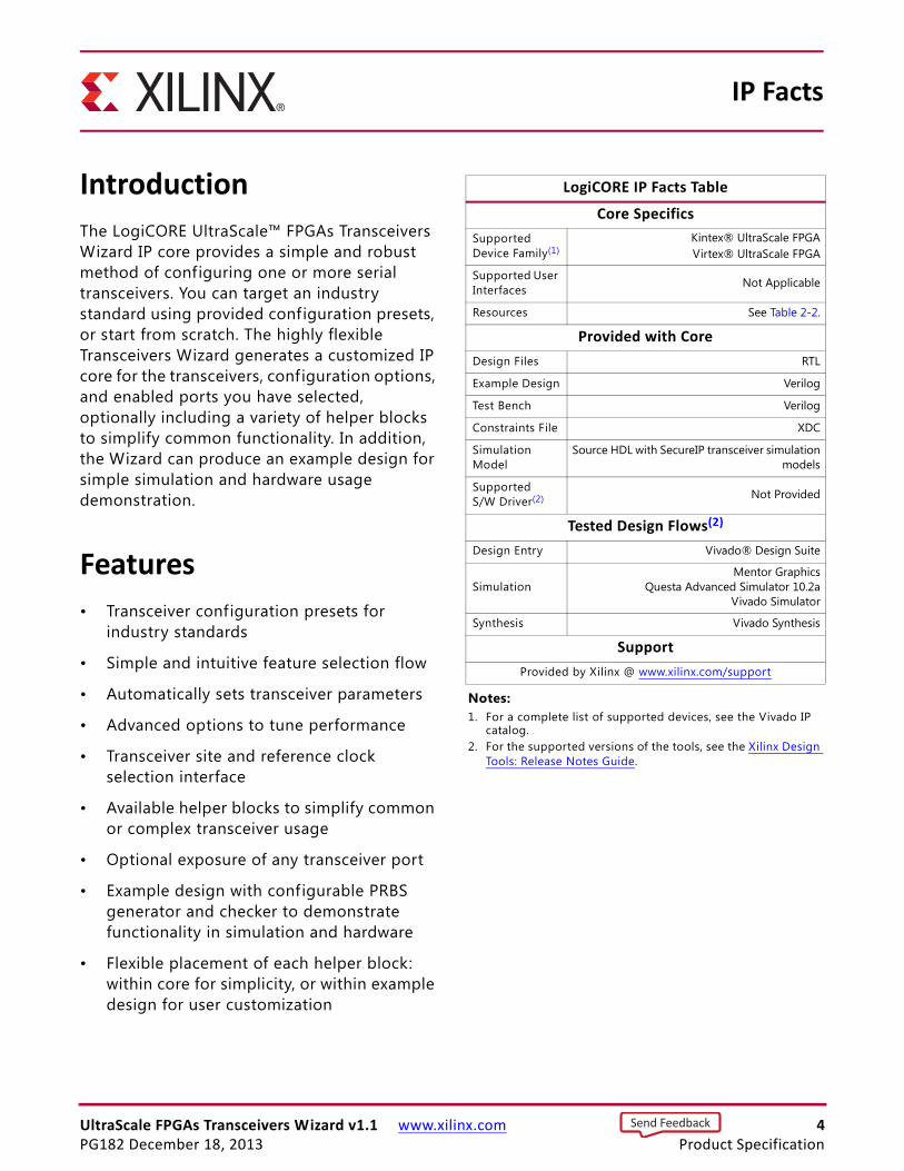
Introduction
The LogiCORE UltraScale™ FPGAs Transceivers Wizard IP core provides a simple and robust method of configuring one or more serial transceivers. You can target an industry standard using provided configuration presets, or start from scratch. The highly flexible Transceivers Wizard generates a customized IP core for the transceivers, configuration options, and enabled ports you have selected, optionally including a variety of helper blocks to simplify common functionality. In addition, the Wizard can produce an example design for simple simulation and hardware usage demonstration.
Features
• Transceiver configuration presets for industry standards
• Simple and intuitive feature selection flow
• Automatically sets transceiver parameters
• Advanced options to tune performance
• Transceiver site and reference clock selection interface
• Available helper blocks to simplify common or complex transceiver usage
• Optional exposure of any transceiver port
• Example design with configurable PRBS generator and checker to demonstrate functionality in simulation and hardware
• Flexible placement of each helper block: within core for simplicity, or within example design for user customization
IP Facts
LogiCORE IP Facts Table
Core Specifics
Supported Device Family(1)
Kintex® UltraScale FPGAVirtex® UltraScale FPGA
Supported User Interfaces Not Applicable
Resources See Table 2-2.
Provided with Core
Design Files RTL
Example Design Verilog
Test Bench Verilog
Constraints File XDC
Simulation Model
Source HDL with SecureIP transceiver simulationmodels
Supported S/W Driver(2) Not Provided
Tested Design Flows(2)
Design Entry Vivado® Design Suite
SimulationMentor Graphics
Questa Advanced Simulator 10.2aVivado Simulator
Synthesis Vivado Synthesis
Support
Provided by Xilinx @ www.xilinx.com/support
Notes: 1. For a complete list of supported devices, see the Vivado IP
catalog.2. For the supported versions of the tools, see the Xilinx Design
Tools: Release Notes Guide.
Send Feedback
UltraScale FPGAs Transceivers Wizard v1.1 www.xilinx.com 5PG182 December 18, 2013
Chapter 1
OverviewThe UltraScale™ FPGAs Transceivers Wizard (Wizard) is used to configure and simplify the use of one or more serial transceivers in a Xilinx UltraScale FPGA. See Chapter 2, Product Specif ication for a detailed description of the core.
This document describes the Wizard IP core. See the UltraScale FPGAs GTH Transceivers User Guide (UG576) [Ref 1] for details on the specif ic use and behavior of the serial transceivers.
Feature SummaryThe Wizard provides these features:
• Customization flow driven by Vivado Integrated Design Environment (Vivado IDE), providing high-level choices that configure supported transceiver features and automatically set primitive parameters, as appropriate
• Variety of transceiver configuration preset selections to target industry standards
• Advanced configuration options to tune transceiver performance
• Transceiver site, reference clock, and recovered clock selection interface for enablement of one or more transceiver channels and adherence to clock routing restrictions
• Optional feature configuration interface for comma detection and alignment, channel bonding, clock correction, and buffer control features
• Available helper blocks to simplify common or complex transceiver usage, and the choice to either include or exclude each helper block from the core
° Helper blocks excluded from the core are delivered as user-customizable starting points within the example design
• Ability to locate enabled transceiver common primitives either within the core or in the example design, and connectivity to simplify resource sharing across multiple cores
• Optional port enablement interface providing the ability to expose any transceiver primitive port as a top-level core port
Send Feedback
UltraScale FPGAs Transceivers Wizard v1.1 www.xilinx.com 6PG182 December 18, 2013
Chapter 1: Overview
• Synthesizable example design with configurable pseudo-random binary sequence (PRBS) data generator and checker logic to quickly demonstrate core and transceiver functionality in simulation and hardware:
° Simulation test bench that monitors example design PRBS lock in loopback
° Additional convenience features, including differential reference clock buffer instantiation and wiring, and per-channel vector slicing
• Core- and example design-level Xilinx Design Constraints (XDC) f iles with timing, location, and other constraints as necessary for the selected configuration
ApplicationsThe Wizard is the supported method of configuring and using one or more serial transceivers in a Xilinx UltraScale FPGA.
Licensing and Ordering InformationThis Xilinx LogiCORE™ IP module is provided at no additional cost with the Xilinx Vivado Design Suite under the terms of the Xilinx End User License. Information about this and other Xilinx LogiCORE IP modules is available at the Xilinx Intellectual Property page. For information about pricing and availability of other Xilinx LogiCORE IP modules and tools, contact your local Xilinx sales representative.
Send Feedback
UltraScale FPGAs Transceivers Wizard v1.1 www.xilinx.com 7PG182 December 18, 2013
Chapter 2
Product SpecificationThe UltraScale™ FPGAs Transceivers Wizard core is the supported method of configuring and using one or more serial transceivers in a Xilinx UltraScale FPGA. In addition to automatically setting primitive parameters as appropriate for your application, the Wizard simplif ies serial transceiver usage by providing a variety of port enablement and helper block convenience functions. These concepts, as well as technical specif ications, are described in this chapter.
Wizard Basic ConceptsTransceiver primitives. Fundamentally, the Wizard instantiates, configures, and connects one or more serial transceiver primitives to provide a simplif ied user interface to those resources. The core instance configures the channel and common primitives by applying HDL parameter values derived from the Vivado® IDE-driven customization of that instance.
Transceiver configuration presets. During Vivado IDE-driven customization, you can choose from a variety of transceiver configuration presets to target an industry standard. If required, customization settings can be further modif ied to suit your application.
Optional port enablement. Xilinx serial transceiver primitives have many ports, and most ports are usually not required for any one use mode. The Wizard provides access to all transceiver primitive ports using an optional port enablement interface, but by default offers a compact user interface by exposing only those ports likely to be necessary for the core as customized.
Helper blocks. The Wizard provides optional modules called helper blocks that abstract or automate certain common or complex transceiver usage procedures. Each helper block can be located either within the core or outside it, delivered with the example design as a user-modif iable starting point. Helper blocks in this release include:
• Reset controller. Controls and abstracts the transceiver reset sequence.
• Transmitter user clocking network . Contains resources to drive the transmitter user clocking network.
• Receiver user clocking network . Contains resources to drive the receiver user clocking network.
Send Feedback
UltraScale FPGAs Transceivers Wizard v1.1 www.xilinx.com 8PG182 December 18, 2013
Chapter 2: Product Specification
• User data width sizing. Sizes the transmitter and receiver data vectors to the specified user widths.
• Transmitter buffer bypass controller. Controls and abstracts the transmitter buffer bypass procedure, if required.
• Receiver buffer bypass controller. Controls and abstracts the receiver buffer bypass procedure, if required.
The Wizard is intended to simplify the use of the serial transceivers. However, it is still important to understand the behavior, usage, and any limitations of the transceivers. See the UltraScale FPGAs GTH Transceivers User Guide (UG576) [Ref 1] for details.
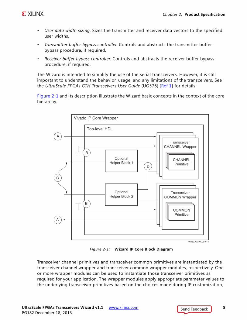
Figure 2-1 and its description illustrate the Wizard basic concepts in the context of the core hierarchy.
Transceiver channel primitives and transceiver common primitives are instantiated by the transceiver channel wrapper and transceiver common wrapper modules, respectively. One or more wrapper modules can be used to instantiate those transceiver primitives as required for your application. The wrapper modules apply appropriate parameter values to the underlying transceiver primitives based on the choices made during IP customization,
X-Ref Target - Figure 2-1
Figure 2‐1: Wizard IP Core Block Diagram
Vivado IP Core Wrapper
Top-level HDL
TransceiverCHANNEL Wrapper
CHANNELPrimitive
TransceiverCOMMON Wrapper
COMMONPrimitive
OptionalHelper Block 2
OptionalHelper Block 1
A
B
C
D
B’
A’
PG182_c2_01_091913
Send Feedback
UltraScale FPGAs Transceivers Wizard v1.1 www.xilinx.com 9PG182 December 18, 2013
Chapter 2: Product Specification
or according to the selected transceiver configuration preset. These wrappers, like the rest of the core hierarchy, should not be user-modif ied.
To provide a compact user interface, only those transceiver primitive ports that are likely needed for the selected configuration are exposed as Wizard IP core-level ports by default. Input vector A represents an enabled core port that drives a corresponding input port of one or more transceiver channel primitives. Likewise, output vector A' is driven by a corresponding output port of one or more transceiver common primitives. If not enabled by default, user-required ports can be individually enabled during IP customization for maximum flexibility.
Transceiver primitive input ports that are not exposed through the core boundary are tied off to their appropriate values (per the core customization) within the Vivado IP core wrapper. Net B represents an input port of one or more transceiver channel primitives that is not enabled as a core port and is automatically tied Low by the Wizard. Net B' represents an analogous transceiver common primitive input, tied High.
The Wizard provides optional helper blocks to simplify common or complex transceiver usage, and each helper block can be located either within the core or within the user-modif iable example design. Vectors C represent the simple user interface of the optional helper blocks when located within the core, while nets D represent the more complex interface between those helper blocks and the transceiver channel and/or common primitives to which they connect.
PerformanceThe Wizard is designed to operate in coordination with the performance characteristics of the transceiver primitives it instantiates.
Maximum Frequencies
See the Kintex UltraScale Architecture Data Sheet: DC and AC Switching Characteristics (DS892) [Ref 2] for the serial transceiver switching characteristics and the serial transceiver user clock switching characteristics for your device. The frequency ranges specified by these documents must be adhered to for proper transceiver and core operation.
IMPORTANT: A free-running clock input, gtwiz_reset_clk_freerun_in, is required by the reset controller helper block to reset the transceiver primitives. As shown in Table 2-1, the maximum frequency of this clock must not exceed the slower of the transceiver channels' two user clock frequencies for the core as customized. The free-running clock must not be derived from either user clock or their sources.
Send Feedback
UltraScale FPGAs Transceivers Wizard v1.1 www.xilinx.com 10PG182 December 18, 2013
Chapter 2: Product Specification
Other Performance Characteristics
See the UltraScale FPGAs GTH Transceivers User Guide (UG576) [Ref 1] for other performance characteristics of the transceiver primitives.
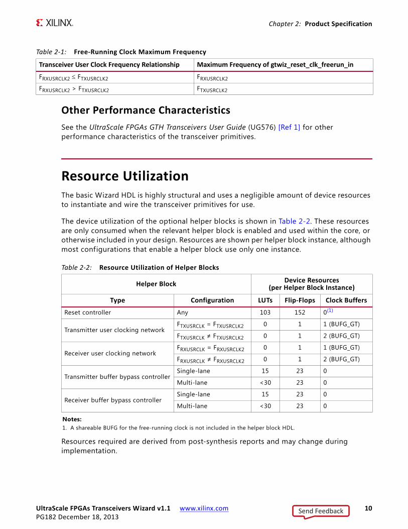
Resource UtilizationThe basic Wizard HDL is highly structural and uses a negligible amount of device resources to instantiate and wire the transceiver primitives for use.
The device utilization of the optional helper blocks is shown in Table 2-2. These resources are only consumed when the relevant helper block is enabled and used within the core, or otherwise included in your design. Resources are shown per helper block instance, although most configurations that enable a helper block use only one instance.
Resources required are derived from post-synthesis reports and may change during implementation.
Table 2‐1: Free‐Running Clock Maximum Frequency
Transceiver User Clock Frequency Relationship Maximum Frequency of gtwiz_reset_clk_freerun_in
FRXUSRCLK2 FTXUSRCLK2 FRXUSRCLK2
FRXUSRCLK2 > FTXUSRCLK2 FTXUSRCLK2
Table 2‐2: Resource Utilization of Helper Blocks
Helper BlockDevice Resources
(per Helper Block Instance)
Type Configuration LUTs Flip‐Flops Clock Buffers
Reset controller Any 103 152 0(1)
Transmitter user clocking networkFTXUSRCLK = FTXUSRCLK2 0 1 1 (BUFG_GT)
FTXUSRCLK ≠ FTXUSRCLK2 0 1 2 (BUFG_GT)
Receiver user clocking networkFRXUSRCLK = FRXUSRCLK2 0 1 1 (BUFG_GT)
FRXUSRCLK ≠ FRXUSRCLK2 0 1 2 (BUFG_GT)
Transmitter buffer bypass controllerSingle-lane 15 23 0
Multi-lane <30 23 0
Receiver buffer bypass controllerSingle-lane 15 23 0
Multi-lane <30 23 0
Notes: 1. A shareable BUFG for the free-running clock is not included in the helper block HDL.
Send Feedback
UltraScale FPGAs Transceivers Wizard v1.1 www.xilinx.com 11PG182 December 18, 2013
Chapter 2: Product Specification
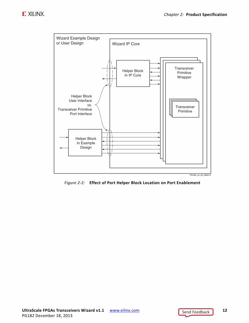
Port DescriptionsThe Wizard enables access to underlying transceiver primitive ports as needed, as well as providing a user interface to enable the helper blocks that are included within the core instance. As such, the Wizard user interface can vary signif icantly between different customizations.
To provide a compact interface, only those transceiver primitive ports that are likely needed for the selected customization are exposed as Wizard IP core-level ports. Additional user-required ports can be individually enabled during IP customization using a flexible optional port enablement interface. See Chapter 4, Customizing and Generating the Core, for details on optional port enablement.
The presence and location of helper blocks also affects the core user interface. When a helper block is enabled and located within the core, a simple user interface is available at the core boundary instead of at the transceiver primitive ports to which it connects. When the helper block is located within the example design, the more complex transceiver primitive ports it connects to are necessarily enabled at the core boundary. Figure 2-2 illustrates how helper block location affects core port enablement.
Send Feedback
UltraScale FPGAs Transceivers Wizard v1.1 www.xilinx.com 12PG182 December 18, 2013
Chapter 2: Product Specification
X-Ref Target - Figure 2-2
Figure 2‐2: Effect of Port Helper Block Location on Port Enablement
Wizard Example Designor User Design Wizard IP Core
TransceiverPrimitiveWrapper
TransceiverPrimitive
Helper BlockIn IP Core
Helper BlockIn Example
Design
Helper BlockUser Interface
vs.Transceiver Primitive
Port Interface
PG182_c2_02_090413
Send Feedback
UltraScale FPGAs Transceivers Wizard v1.1 www.xilinx.com 13PG182 December 18, 2013
Chapter 2: Product Specification
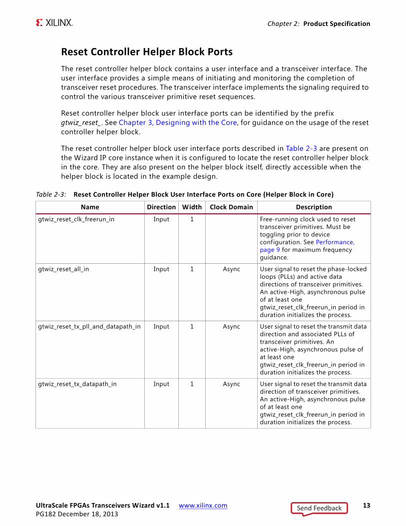
Reset Controller Helper Block Ports
The reset controller helper block contains a user interface and a transceiver interface. The user interface provides a simple means of initiating and monitoring the completion of transceiver reset procedures. The transceiver interface implements the signaling required to control the various transceiver primitive reset sequences.
Reset controller helper block user interface ports can be identif ied by the prefix gtwiz_reset_. See Chapter 3, Designing with the Core, for guidance on the usage of the reset controller helper block.
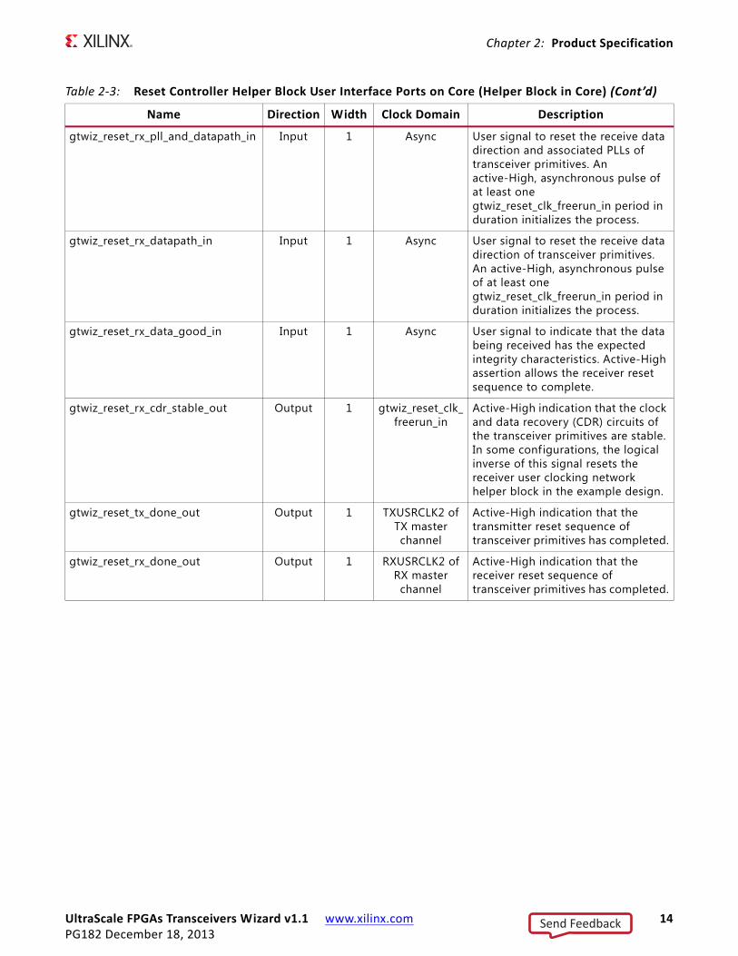
The reset controller helper block user interface ports described in Table 2-3 are present on the Wizard IP core instance when it is configured to locate the reset controller helper block in the core. They are also present on the helper block itself, directly accessible when the helper block is located in the example design.
Table 2‐3: Reset Controller Helper Block User Interface Ports on Core (Helper Block in Core)
Name Direction Width Clock Domain Description
gtwiz_reset_clk_freerun_in Input 1 Free-running clock used to reset transceiver primitives. Must be toggling prior to device configuration. See Performance, page 9 for maximum frequency guidance.
gtwiz_reset_all_in Input 1 Async User signal to reset the phase-locked loops (PLLs) and active data directions of transceiver primitives. An active-High, asynchronous pulse of at least one gtwiz_reset_clk_freerun_in period in duration initializes the process.
gtwiz_reset_tx_pll_and_datapath_in Input 1 Async User signal to reset the transmit data direction and associated PLLs of transceiver primitives. An active-High, asynchronous pulse of at least one gtwiz_reset_clk_freerun_in period in duration initializes the process.
gtwiz_reset_tx_datapath_in Input 1 Async User signal to reset the transmit data direction of transceiver primitives. An active-High, asynchronous pulse of at least one gtwiz_reset_clk_freerun_in period in duration initializes the process.
Send Feedback
UltraScale FPGAs Transceivers Wizard v1.1 www.xilinx.com 14PG182 December 18, 2013
Chapter 2: Product Specification
gtwiz_reset_rx_pll_and_datapath_in Input 1 Async User signal to reset the receive data direction and associated PLLs of transceiver primitives. An active-High, asynchronous pulse of at least one gtwiz_reset_clk_freerun_in period in duration initializes the process.
gtwiz_reset_rx_datapath_in Input 1 Async User signal to reset the receive data direction of transceiver primitives. An active-High, asynchronous pulse of at least one gtwiz_reset_clk_freerun_in period in duration initializes the process.
gtwiz_reset_rx_data_good_in Input 1 Async User signal to indicate that the data being received has the expected integrity characteristics. Active-High assertion allows the receiver reset sequence to complete.
gtwiz_reset_rx_cdr_stable_out Output 1 gtwiz_reset_clk_freerun_in
Active-High indication that the clock and data recovery (CDR) circuits of the transceiver primitives are stable. In some configurations, the logical inverse of this signal resets the receiver user clocking network helper block in the example design.
gtwiz_reset_tx_done_out Output 1 TXUSRCLK2 of TX master channel
Active-High indication that the transmitter reset sequence of transceiver primitives has completed.
gtwiz_reset_rx_done_out Output 1 RXUSRCLK2 of RX master channel
Active-High indication that the receiver reset sequence of transceiver primitives has completed.
Table 2‐3: Reset Controller Helper Block User Interface Ports on Core (Helper Block in Core) (Cont’d)
Name Direction Width Clock Domain Description
Send Feedback
UltraScale FPGAs Transceivers Wizard v1.1 www.xilinx.com 15PG182 December 18, 2013
Chapter 2: Product Specification
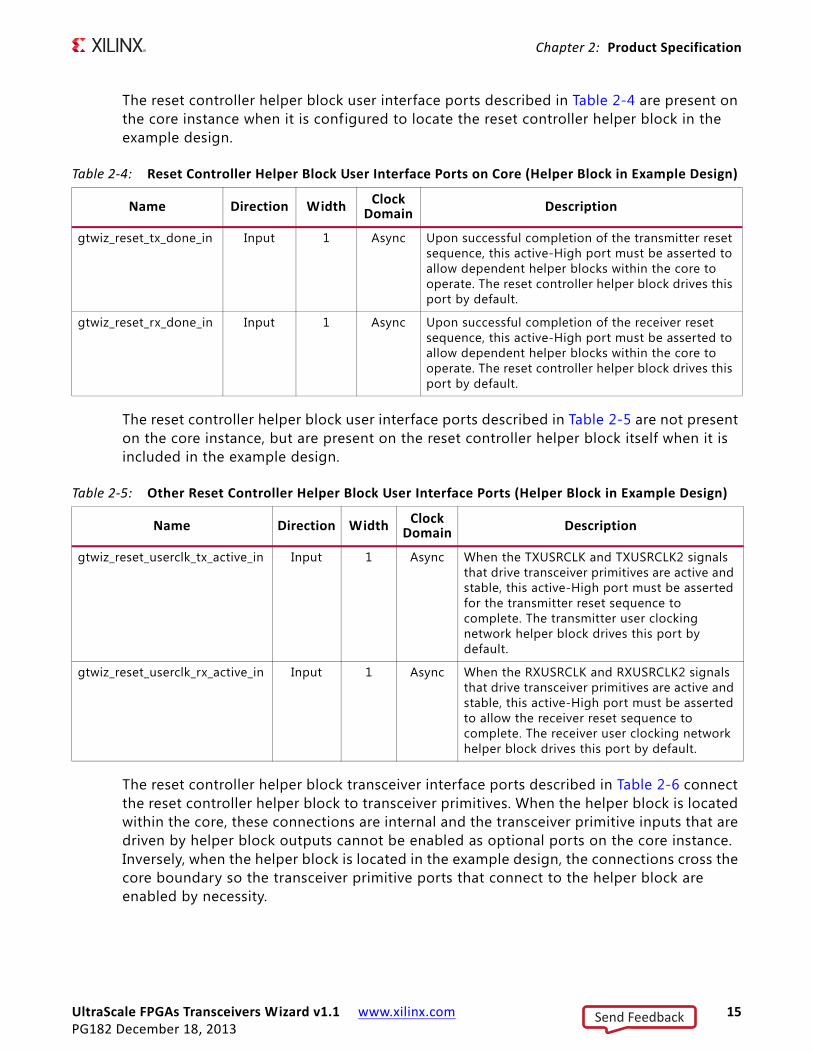
The reset controller helper block user interface ports described in Table 2-4 are present on the core instance when it is configured to locate the reset controller helper block in the example design.
The reset controller helper block user interface ports described in Table 2-5 are not present on the core instance, but are present on the reset controller helper block itself when it is included in the example design.
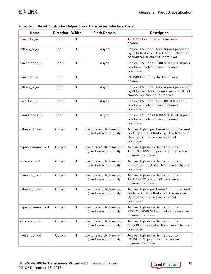
The reset controller helper block transceiver interface ports described in Table 2-6 connect the reset controller helper block to transceiver primitives. When the helper block is located within the core, these connections are internal and the transceiver primitive inputs that are driven by helper block outputs cannot be enabled as optional ports on the core instance. Inversely, when the helper block is located in the example design, the connections cross the core boundary so the transceiver primitive ports that connect to the helper block are enabled by necessity.
Table 2‐4: Reset Controller Helper Block User Interface Ports on Core (Helper Block in Example Design)
Name Direction WidthClock
DomainDescription
gtwiz_reset_tx_done_in Input 1 Async Upon successful completion of the transmitter reset sequence, this active-High port must be asserted to allow dependent helper blocks within the core to operate. The reset controller helper block drives this port by default.
gtwiz_reset_rx_done_in Input 1 Async Upon successful completion of the receiver reset sequence, this active-High port must be asserted to allow dependent helper blocks within the core to operate. The reset controller helper block drives this port by default.
Table 2‐5: Other Reset Controller Helper Block User Interface Ports (Helper Block in Example Design)
Name Direction Width Clock Domain
Description
gtwiz_reset_userclk_tx_active_in Input 1 Async When the TXUSRCLK and TXUSRCLK2 signals that drive transceiver primitives are active and stable, this active-High port must be asserted for the transmitter reset sequence to complete. The transmitter user clocking network helper block drives this port by default.
gtwiz_reset_userclk_rx_active_in Input 1 Async When the RXUSRCLK and RXUSRCLK2 signals that drive transceiver primitives are active and stable, this active-High port must be asserted to allow the receiver reset sequence to complete. The receiver user clocking network helper block drives this port by default.
Send Feedback
UltraScale FPGAs Transceivers Wizard v1.1 www.xilinx.com 16PG182 December 18, 2013
Chapter 2: Product Specification
Table 2‐6: Reset Controller Helper Block Transceiver Interface Ports
Name Direction Width Clock Domain Description
txusrclk2_in Input 1 TXUSRCLK2 of master transceiver channel.
plllock_tx_in Input 1 Async Logical AND of all lock signals produced by PLLs that clock the transmit datapath of transceiver channel primitives.
txresetdone_in Input 1 Async Logical AND of all TXRESETDONE signals produced by transceiver channel primitives.
rxusrclk2_in Input 1 RXUSRCLK2 of master transceiver channel.
plllock_rx_in Input 1 Async Logical AND of all lock signals produced by PLLs that clock the receive datapath of transceiver channel primitives.
rxcdrlock_in Input 1 Async Logical AND of all RXCDRLOCK signals produced by transceiver channel primitives.
rxresetdone_in Input 1 Async Logical AND of all RXRESETDONE signals produced by transceiver channel primitives.
pllreset_tx_out Output 1 gtwiz_reset_clk_freerun_in (used asynchronously)
Active-High signal fanned out to the reset ports of all PLLs that clock the transmit datapath of transceiver channel primitives.
txprogdivreset_out Output 1 gtwiz_reset_clk_freerun_in (used asynchronously)
Active-High signal fanned out to TXPROGDIVRESET port of all transceiver channel primitives.
gttxreset_out Output 1 gtwiz_reset_clk_freerun_in (used asynchronously)
Active-High signal fanned out to GTTXRESET port of all transceiver channel primitives.
txuserrdy_out Output 1 gtwiz_reset_clk_freerun_in (used asynchronously)
Active-High signal fanned out to TXUSERRDY port of all transceiver channel primitives.
pllreset_rx_out Output 1 gtwiz_reset_clk_freerun_in (used asynchronously)
Active-High signal fanned out to the reset ports of all PLLs that clock the receive datapath of transceiver channel primitives.
rxprogdivreset_out Output 1 gtwiz_reset_clk_freerun_in (used asynchronously)
Active-High signal fanned out to RXPROGDIVRESET port of all transceiver channel primitives.
gtrxreset_out Output 1 gtwiz_reset_clk_freerun_in (used asynchronously)
Active-High signal fanned out to GTRXRESET port of all transceiver channel primitives.
rxuserrdy_out Output 1 gtwiz_reset_clk_freerun_in (used asynchronously)
Active-High signal fanned out to RXUSERRDY port of all transceiver channel primitives.
Send Feedback
UltraScale FPGAs Transceivers Wizard v1.1 www.xilinx.com 17PG182 December 18, 2013
Chapter 2: Product Specification
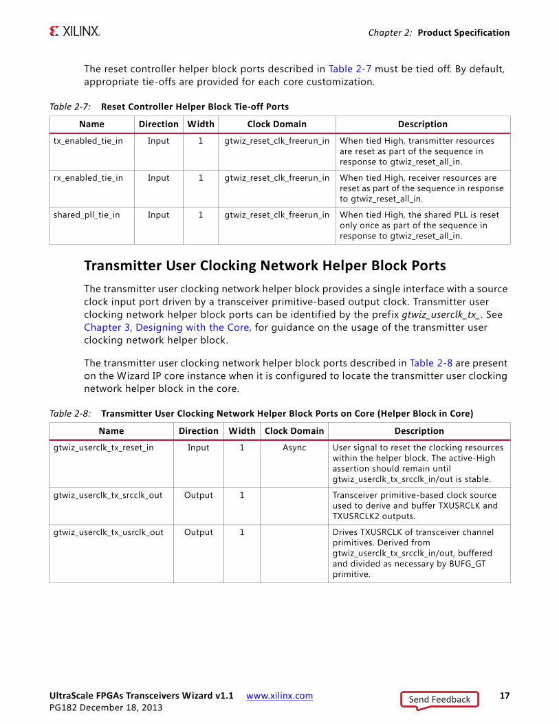
The reset controller helper block ports described in Table 2-7 must be tied off. By default, appropriate tie-offs are provided for each core customization.
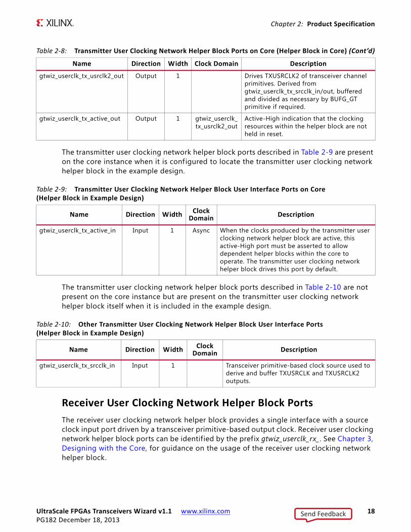
Transmitter User Clocking Network Helper Block Ports
The transmitter user clocking network helper block provides a single interface with a source clock input port driven by a transceiver primitive-based output clock. Transmitter user clocking network helper block ports can be identif ied by the prefix gtwiz_userclk_tx_. See Chapter 3, Designing with the Core, for guidance on the usage of the transmitter user clocking network helper block.
The transmitter user clocking network helper block ports described in Table 2-8 are present on the Wizard IP core instance when it is configured to locate the transmitter user clocking network helper block in the core.
Table 2‐7: Reset Controller Helper Block Tie‐off Ports
Name Direction Width Clock Domain Description
tx_enabled_tie_in Input 1 gtwiz_reset_clk_freerun_in When tied High, transmitter resources are reset as part of the sequence in response to gtwiz_reset_all_in.
rx_enabled_tie_in Input 1 gtwiz_reset_clk_freerun_in When tied High, receiver resources are reset as part of the sequence in response to gtwiz_reset_all_in.
shared_pll_tie_in Input 1 gtwiz_reset_clk_freerun_in When tied High, the shared PLL is reset only once as part of the sequence in response to gtwiz_reset_all_in.
Table 2‐8: Transmitter User Clocking Network Helper Block Ports on Core (Helper Block in Core)
Name Direction Width Clock Domain Description
gtwiz_userclk_tx_reset_in Input 1 Async User signal to reset the clocking resources within the helper block. The active-High assertion should remain until gtwiz_userclk_tx_srcclk_in/out is stable.
gtwiz_userclk_tx_srcclk_out Output 1 Transceiver primitive-based clock source used to derive and buffer TXUSRCLK and TXUSRCLK2 outputs.
gtwiz_userclk_tx_usrclk_out Output 1 Drives TXUSRCLK of transceiver channel primitives. Derived from gtwiz_userclk_tx_srcclk_in/out, buffered and divided as necessary by BUFG_GT primitive.
Send Feedback
UltraScale FPGAs Transceivers Wizard v1.1 www.xilinx.com 18PG182 December 18, 2013
Chapter 2: Product Specification
The transmitter user clocking network helper block ports described in Table 2-9 are present on the core instance when it is configured to locate the transmitter user clocking network helper block in the example design.
The transmitter user clocking network helper block ports described in Table 2-10 are not present on the core instance but are present on the transmitter user clocking network helper block itself when it is included in the example design.
Receiver User Clocking Network Helper Block Ports
The receiver user clocking network helper block provides a single interface with a source clock input port driven by a transceiver primitive-based output clock. Receiver user clocking network helper block ports can be identif ied by the prefix gtwiz_userclk_rx_. See Chapter 3, Designing with the Core, for guidance on the usage of the receiver user clocking network helper block.
gtwiz_userclk_tx_usrclk2_out Output 1 Drives TXUSRCLK2 of transceiver channel primitives. Derived from gtwiz_userclk_tx_srcclk_in/out, buffered and divided as necessary by BUFG_GT primitive if required.
gtwiz_userclk_tx_active_out Output 1 gtwiz_userclk_tx_usrclk2_out
Active-High indication that the clocking resources within the helper block are not held in reset.
Table 2‐8: Transmitter User Clocking Network Helper Block Ports on Core (Helper Block in Core) (Cont’d)
Name Direction Width Clock Domain Description
Table 2‐9: Transmitter User Clocking Network Helper Block User Interface Ports on Core (Helper Block in Example Design)
Name Direction Width Clock Domain
Description
gtwiz_userclk_tx_active_in Input 1 Async When the clocks produced by the transmitter user clocking network helper block are active, this active-High port must be asserted to allow dependent helper blocks within the core to operate. The transmitter user clocking network helper block drives this port by default.
Table 2‐10: Other Transmitter User Clocking Network Helper Block User Interface Ports (Helper Block in Example Design)
Name Direction WidthClock
Domain Description
gtwiz_userclk_tx_srcclk_in Input 1 Transceiver primitive-based clock source used to derive and buffer TXUSRCLK and TXUSRCLK2 outputs.
Send Feedback
UltraScale FPGAs Transceivers Wizard v1.1 www.xilinx.com 19PG182 December 18, 2013
Chapter 2: Product Specification
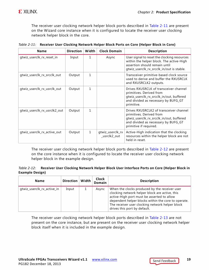
The receiver user clocking network helper block ports described in Table 2-11 are present on the Wizard core instance when it is configured to locate the receiver user clocking network helper block in the core.
The receiver user clocking network helper block ports described in Table 2-12 are present on the core instance when it is configured to locate the receiver user clocking network helper block in the example design.
The receiver user clocking network helper block ports described in Table 2-13 are not present on the core instance, but are present on the receiver user clocking network helper block itself when it is included in the example design.
Table 2‐11: Receiver User Clocking Network Helper Block Ports on Core (Helper Block in Core)
Name Direction Width Clock Domain Description
gtwiz_userclk_rx_reset_in Input 1 Async User signal to reset the clocking resources within the helper block. The active-High assertion should remain until gtwiz_userclk_rx_srcclk_in/out is stable.
gtwiz_userclk_rx_srcclk_out Output 1 Transceiver primitive-based clock source used to derive and buffer the RXUSRCLK and RXUSRCLK2 outputs.
gtwiz_userclk_rx_usrclk_out Output 1 Drives RXUSRCLK of transceiver channel primitives. Derived from gtwiz_userclk_rx_srcclk_in/out, buffered and divided as necessary by BUFG_GT primitive.
gtwiz_userclk_rx_usrclk2_out Output 1 Drives RXUSRCLK2 of transceiver channel primitives. Derived from gtwiz_userclk_rx_srcclk_in/out, buffered and divided as necessary by BUFG_GT primitive if required.
gtwiz_userclk_rx_active_out Output 1 gtwiz_userclk_rx_usrclk2_out
Active-High indication that the clocking resources within the helper block are not held in reset.
Table 2‐12: Receiver User Clocking Network Helper Block User Interface Ports on Core (Helper Block in Example Design)
Name Direction Width Clock Domain
Description
gtwiz_userclk_rx_active_in Input 1 Async When the clocks produced by the receiver user clocking network helper block are active, this active-High port must be asserted to allow dependent helper blocks within the core to operate. The receiver user clocking network helper block drives this port by default.
Send Feedback
UltraScale FPGAs Transceivers Wizard v1.1 www.xilinx.com 20PG182 December 18, 2013
Chapter 2: Product Specification
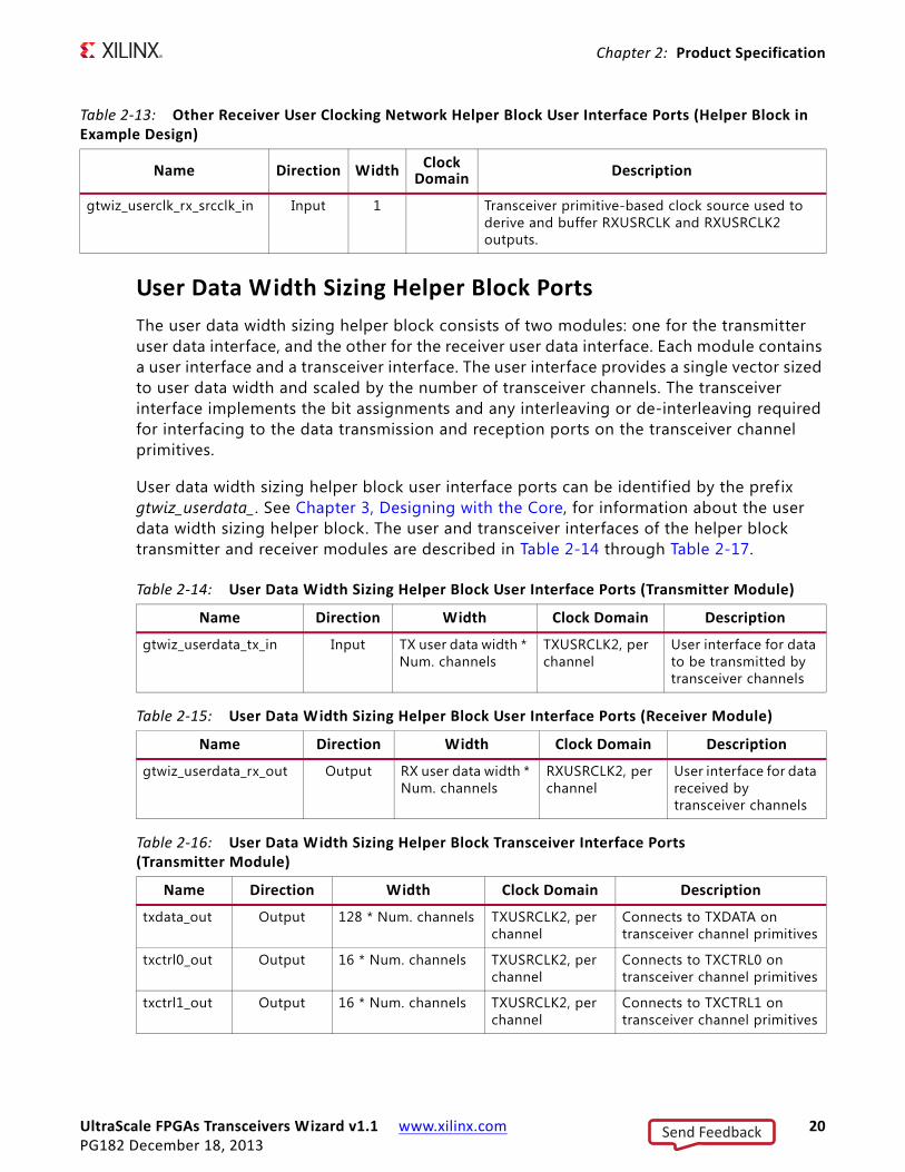
User Data Width Sizing Helper Block Ports
The user data width sizing helper block consists of two modules: one for the transmitter user data interface, and the other for the receiver user data interface. Each module contains a user interface and a transceiver interface. The user interface provides a single vector sized to user data width and scaled by the number of transceiver channels. The transceiver interface implements the bit assignments and any interleaving or de-interleaving required for interfacing to the data transmission and reception ports on the transceiver channel primitives.
User data width sizing helper block user interface ports can be identif ied by the prefix gtwiz_userdata_. See Chapter 3, Designing with the Core, for information about the user data width sizing helper block. The user and transceiver interfaces of the helper block transmitter and receiver modules are described in Table 2-14 through Table 2-17.
Table 2‐13: Other Receiver User Clocking Network Helper Block User Interface Ports (Helper Block in Example Design)
Name Direction Width Clock Domain
Description
gtwiz_userclk_rx_srcclk_in Input 1 Transceiver primitive-based clock source used to derive and buffer RXUSRCLK and RXUSRCLK2 outputs.
Table 2‐14: User Data Width Sizing Helper Block User Interface Ports (Transmitter Module)
Name Direction Width Clock Domain Description
gtwiz_userdata_tx_in Input TX user data width * Num. channels
TXUSRCLK2, per channel
User interface for data to be transmitted by transceiver channels
Table 2‐15: User Data Width Sizing Helper Block User Interface Ports (Receiver Module)
Name Direction Width Clock Domain Description
gtwiz_userdata_rx_out Output RX user data width * Num. channels
RXUSRCLK2, per channel
User interface for data received by transceiver channels
Table 2‐16: User Data Width Sizing Helper Block Transceiver Interface Ports (Transmitter Module)
Name Direction Width Clock Domain Description
txdata_out Output 128 * Num. channels TXUSRCLK2, per channel
Connects to TXDATA on transceiver channel primitives
txctrl0_out Output 16 * Num. channels TXUSRCLK2, per channel
Connects to TXCTRL0 on transceiver channel primitives
txctrl1_out Output 16 * Num. channels TXUSRCLK2, per channel
Connects to TXCTRL1 on transceiver channel primitives
Send Feedback
UltraScale FPGAs Transceivers Wizard v1.1 www.xilinx.com 21PG182 December 18, 2013
Chapter 2: Product Specification
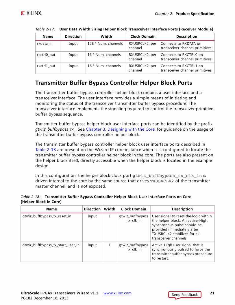
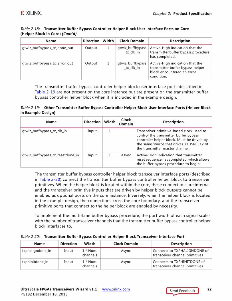
Transmitter Buffer Bypass Controller Helper Block Ports
The transmitter buffer bypass controller helper block contains a user interface and a transceiver interface. The user interface provides a simple means of initiating and monitoring the status of the transceiver transmitter buffer bypass procedure. The transceiver interface implements the signaling required to control the transceiver primitive buffer bypass sequence.
Transmitter buffer bypass helper block user interface ports can be identif ied by the prefix gtwiz_buffbypass_tx_. See Chapter 3, Designing with the Core, for guidance on the usage of the transmitter buffer bypass controller helper block.
The transmitter buffer bypass controller helper block user interface ports described in Table 2-18 are present on the Wizard IP core instance when it is configured to locate the transmitter buffer bypass controller helper block in the core. The ports are also present on the helper block itself, directly accessible when the helper block is located in the example design.
In this configuration, the helper block clock port gtwiz_buffbypass_tx_clk_in is driven internal to the core by the same source that drives TXUSRCLK2 of the transmitter master channel, and is not exposed.
Table 2‐17: User Data Width Sizing Helper Block Transceiver Interface Ports (Receiver Module)
Name Direction Width Clock Domain Description
rxdata_in Input 128 * Num. channels RXUSRCLK2, per channel
Connects to RXDATA on transceiver channel primitives
rxctrl0_out Input 16 * Num. channels RXUSRCLK2, per channel
Connects to RXCTRL0 on transceiver channel primitives
rxctrl1_out Input 16 * Num. channels RXUSRCLK2, per channel
Connects to RXCTRL1 on transceiver channel primitives
Table 2‐18: Transmitter Buffer Bypass Controller Helper Block User Interface Ports on Core (Helper Block in Core)
Name Direction Width Clock Domain Description
gtwiz_buffbypass_tx_reset_in Input 1 gtwiz_buffbypass_tx_clk_in
User signal to reset the logic within the helper block. An active-High, synchronous pulse should be provided immediately after TXUSRCLK2 stabilizes for all transceiver channels.
gtwiz_buffbypass_tx_start_user_in Input 1 gtwiz_buffbypass_tx_clk_in
Active-High user signal that is synchronously pulsed to force the transmitter buffer bypass procedure to restart.
Send Feedback
UltraScale FPGAs Transceivers Wizard v1.1 www.xilinx.com 22PG182 December 18, 2013
Chapter 2: Product Specification
The transmitter buffer bypass controller helper block user interface ports described in Table 2-19 are not present on the core instance but are present on the transmitter buffer bypass controller helper block when it is included in the example design.
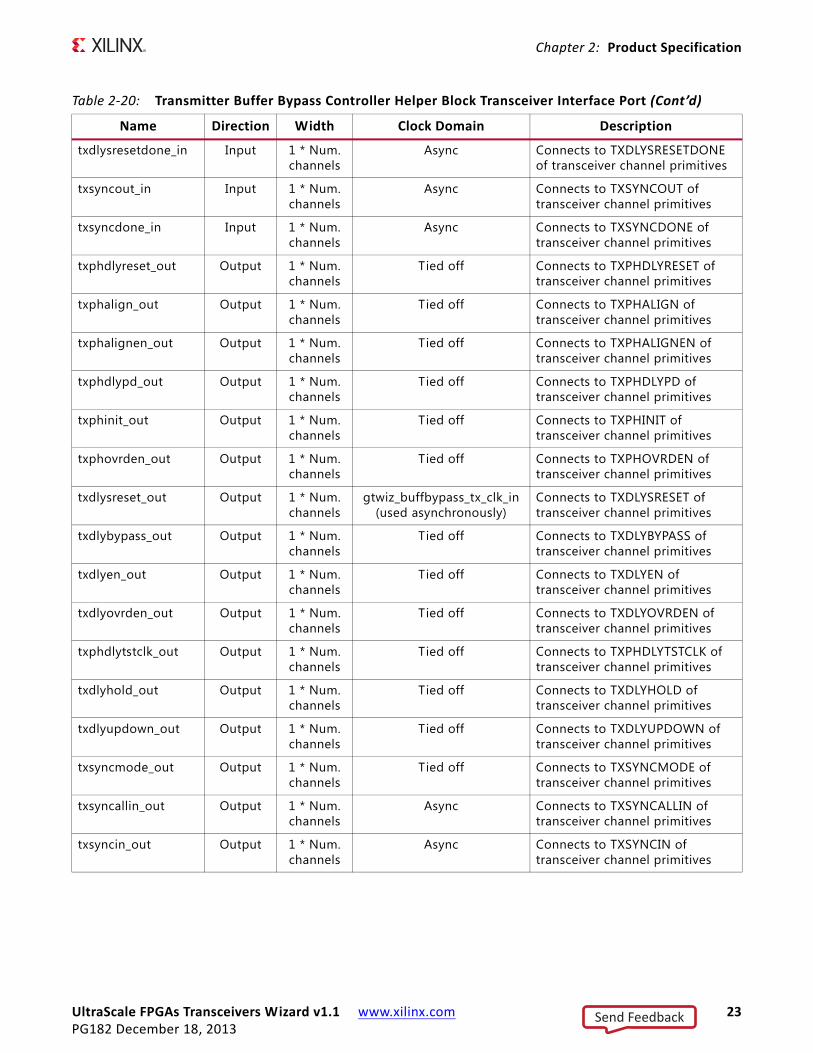
The transmitter buffer bypass controller helper block transceiver interface ports (described in Table 2-20) connect the transmitter buffer bypass controller helper block to transceiver primitives. When the helper block is located within the core, these connections are internal, and the transceiver primitive inputs that are driven by helper block outputs cannot be enabled as optional ports on the core instance. Inversely, when the helper block is located in the example design, the connections cross the core boundary, and the transceiver primitive ports that connect to the helper block are enabled by necessity.
To implement the multi-lane buffer bypass procedure, the port width of each signal scales with the number of transceiver channels that the transmitter buffer bypass controller helper block interfaces to.
gtwiz_buffbypass_tx_done_out Output 1 gtwiz_buffbypass_tx_clk_in
Active-High indication that the transmitter buffer bypass procedure has completed.
gtwiz_buffbypass_tx_error_out Output 1 gtwiz_buffbypass_tx_clk_in
Active-High indication that the transmitter buffer bypass helper block encountered an error condition.
Table 2‐18: Transmitter Buffer Bypass Controller Helper Block User Interface Ports on Core (Helper Block in Core) (Cont’d)
Name Direction Width Clock Domain Description
Table 2‐19: Other Transmitter Buffer Bypass Controller Helper Block User Interface Ports (Helper Block in Example Design)
Name Direction Width Clock Domain
Description
gtwiz_buffbypass_tx_clk_in Input 1 Transceiver primitive-based clock used to control the transmitter buffer bypass controller helper block. Must be driven by the same source that drives TXUSRCLK2 of the transmitter master channel.
gtwiz_buffbypass_tx_resetdone_in Input 1 Async Active-High indication that transmitter reset sequence has completed, which allows the buffer bypass procedure to begin.
Table 2‐20: Transmitter Buffer Bypass Controller Helper Block Transceiver Interface Port
Name Direction Width Clock Domain Description
txphaligndone_in Input 1 * Num. channels
Async Connects to TXPHALIGNDONE of transceiver channel primitives
txphinitdone_in Input 1 * Num. channels
Async Connects to TXPHINITDONE of transceiver channel primitives
Send Feedback
UltraScale FPGAs Transceivers Wizard v1.1 www.xilinx.com 23PG182 December 18, 2013
Chapter 2: Product Specification
txdlysresetdone_in Input 1 * Num. channels
Async Connects to TXDLYSRESETDONE of transceiver channel primitives
txsyncout_in Input 1 * Num. channels
Async Connects to TXSYNCOUT of transceiver channel primitives
txsyncdone_in Input 1 * Num. channels
Async Connects to TXSYNCDONE of transceiver channel primitives
txphdlyreset_out Output 1 * Num. channels
Tied off Connects to TXPHDLYRESET of transceiver channel primitives
txphalign_out Output 1 * Num. channels
Tied off Connects to TXPHALIGN of transceiver channel primitives
txphalignen_out Output 1 * Num. channels
Tied off Connects to TXPHALIGNEN of transceiver channel primitives
txphdlypd_out Output 1 * Num. channels
Tied off Connects to TXPHDLYPD of transceiver channel primitives
txphinit_out Output 1 * Num. channels
Tied off Connects to TXPHINIT of transceiver channel primitives
txphovrden_out Output 1 * Num. channels
Tied off Connects to TXPHOVRDEN of transceiver channel primitives
txdlysreset_out Output 1 * Num. channels
gtwiz_buffbypass_tx_clk_in (used asynchronously)
Connects to TXDLYSRESET of transceiver channel primitives
txdlybypass_out Output 1 * Num. channels
Tied off Connects to TXDLYBYPASS of transceiver channel primitives
txdlyen_out Output 1 * Num. channels
Tied off Connects to TXDLYEN of transceiver channel primitives
txdlyovrden_out Output 1 * Num. channels
Tied off Connects to TXDLYOVRDEN of transceiver channel primitives
txphdlytstclk_out Output 1 * Num. channels
Tied off Connects to TXPHDLYTSTCLK of transceiver channel primitives
txdlyhold_out Output 1 * Num. channels
Tied off Connects to TXDLYHOLD of transceiver channel primitives
txdlyupdown_out Output 1 * Num. channels
Tied off Connects to TXDLYUPDOWN of transceiver channel primitives
txsyncmode_out Output 1 * Num. channels
Tied off Connects to TXSYNCMODE of transceiver channel primitives
txsyncallin_out Output 1 * Num. channels
Async Connects to TXSYNCALLIN of transceiver channel primitives
txsyncin_out Output 1 * Num. channels
Async Connects to TXSYNCIN of transceiver channel primitives
Table 2‐20: Transmitter Buffer Bypass Controller Helper Block Transceiver Interface Port (Cont’d)
Name Direction Width Clock Domain Description
Send Feedback
UltraScale FPGAs Transceivers Wizard v1.1 www.xilinx.com 24PG182 December 18, 2013
Chapter 2: Product Specification
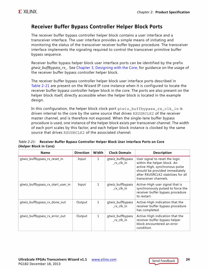
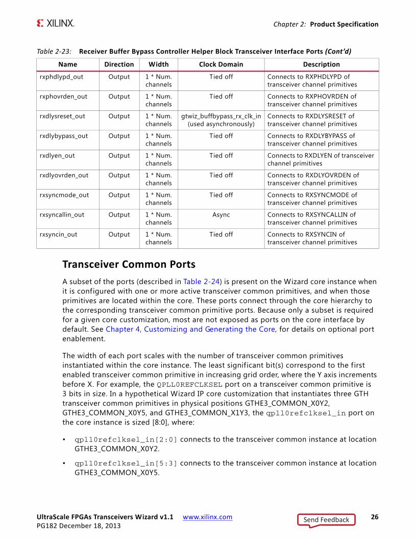
Receiver Buffer Bypass Controller Helper Block Ports
The receiver buffer bypass controller helper block contains a user interface and a transceiver interface. The user interface provides a simple means of initiating and monitoring the status of the transceiver receiver buffer bypass procedure. The transceiver interface implements the signaling required to control the transceiver primitive buffer bypass sequence.
Receiver buffer bypass helper block user interface ports can be identif ied by the prefix gtwiz_buffbypass_rx_. See Chapter 3, Designing with the Core, for guidance on the usage of the receiver buffer bypass controller helper block.
The receiver buffer bypass controller helper block user interface ports described in Table 2-21 are present on the Wizard IP core instance when it is configured to locate the receiver buffer bypass controller helper block in the core. The ports are also present on the helper block itself, directly accessible when the helper block is located in the example design.
In this configuration, the helper block clock port gtwiz_buffbypass_rx_clk_in is driven internal to the core by the same source that drives RXUSRCLK2 of the receiver master channel, and is therefore not exposed. When the single-lane buffer bypass procedure is used, one instance of the helper block exists per transceiver channel. The width of each port scales by this factor, and each helper block instance is clocked by the same source that drives RXUSRCLK2 of the associated channel.
Table 2‐21: Receiver Buffer Bypass Controller Helper Block User Interface Ports on Core (Helper Block in Core)
Name Direction Width Clock Domain Description
gtwiz_buffbypass_rx_reset_in Input 1 gtwiz_buffbypass_rx_clk_in
User signal to reset the logic within the helper block. An active-High, synchronous pulse should be provided immediately after RXUSRCLK2 stabilizes for all transceiver channels.
gtwiz_buffbypass_rx_start_user_in Input 1 gtwiz_buffbypass_rx_clk_in
Active-High user signal that is synchronously pulsed to force the receiver buffer bypass procedure to restart.
gtwiz_buffbypass_rx_done_out Output 1 gtwiz_buffbypass_rx_clk_in
Active-High indication that the receiver buffer bypass procedure has completed.
gtwiz_buffbypass_rx_error_out Output 1 gtwiz_buffbypass_rx_clk_in
Active-High indication that the receiver buffer bypass helper block encountered an error condition.
Send Feedback
UltraScale FPGAs Transceivers Wizard v1.1 www.xilinx.com 25PG182 December 18, 2013
Chapter 2: Product Specification
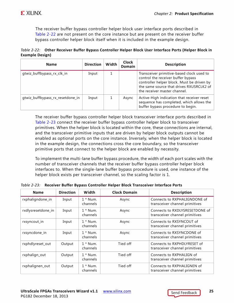
The receiver buffer bypass controller helper block user interface ports described in Table 2-22 are not present on the core instance but are present on the receiver buffer bypass controller helper block itself when it is included in the example design.
The receiver buffer bypass controller helper block transceiver interface ports described in Table 2-23 connect the receiver buffer bypass controller helper block to transceiver primitives. When the helper block is located within the core, these connections are internal, and the transceiver primitive inputs that are driven by helper block outputs cannot be enabled as optional ports on the core instance. Inversely, when the helper block is located in the example design, the connections cross the core boundary, so the transceiver primitive ports that connect to the helper block are enabled by necessity.
To implement the multi-lane buffer bypass procedure, the width of each port scales with the number of transceiver channels that the receiver buffer bypass controller helper block interfaces to. When the single-lane buffer bypass procedure is used, one instance of the helper block exists per transceiver channel, so the scaling factor is 1.
Table 2‐22: Other Receiver Buffer Bypass Controller Helper Block User Interface Ports (Helper Block in Example Design)
Name Direction WidthClock
Domain Description
gtwiz_buffbypass_rx_clk_in Input 1 Transceiver primitive-based clock used to control the receiver buffer bypass controller helper block. Must be driven by the same source that drives RXUSRCLK2 of the receiver master channel.
gtwiz_buffbypass_rx_resetdone_in Input 1 Async Active-High indication that receiver reset sequence has completed, which allows the buffer bypass procedure to begin.
Table 2‐23: Receiver Buffer Bypass Controller Helper Block Transceiver Interface Ports
Name Direction Width Clock Domain Description
rxphaligndone_in Input 1 * Num. channels
Async Connects to RXPHALIGNDONE of transceiver channel primitives
rxdlysresetdone_in Input 1 * Num. channels
Async Connects to RXDLYSRESETDONE of transceiver channel primitives
rxsyncout_in Input 1 * Num. channels
Async Connects to RXSYNCOUT of transceiver channel primitives
rxsyncdone_in Input 1 * Num. channels
Async Connects to RXSYNCDONE of transceiver channel primitives
rxphdlyreset_out Output 1 * Num. channels
Tied off Connects to RXPHDLYRESET of transceiver channel primitives
rxphalign_out Output 1 * Num. channels
Tied off Connects to RXPHALIGN of transceiver channel primitives
rxphalignen_out Output 1 * Num. channels
Tied off Connects to RXPHALIGNEN of transceiver channel primitives
Send Feedback
UltraScale FPGAs Transceivers Wizard v1.1 www.xilinx.com 26PG182 December 18, 2013
Chapter 2: Product Specification
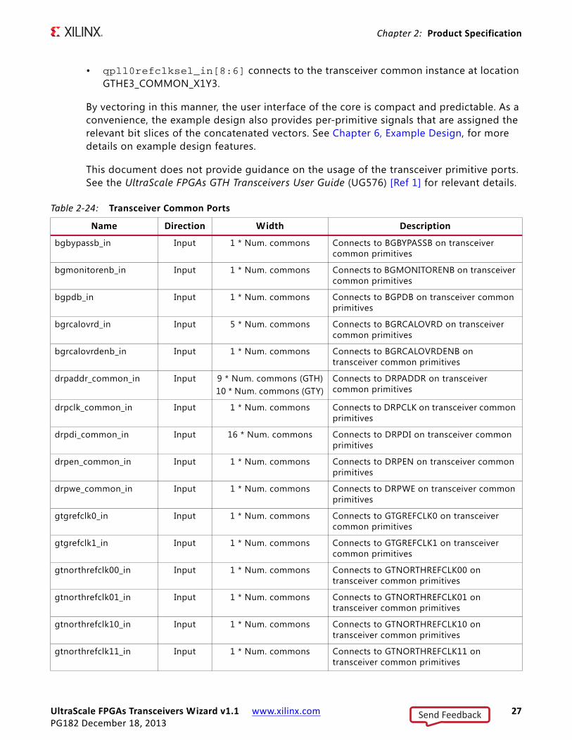
Transceiver Common Ports
A subset of the ports (described in Table 2-24) is present on the Wizard core instance when it is configured with one or more active transceiver common primitives, and when those primitives are located within the core. These ports connect through the core hierarchy to the corresponding transceiver common primitive ports. Because only a subset is required for a given core customization, most are not exposed as ports on the core interface by default. See Chapter 4, Customizing and Generating the Core, for details on optional port enablement.
The width of each port scales with the number of transceiver common primitives instantiated within the core instance. The least significant bit(s) correspond to the f irst enabled transceiver common primitive in increasing grid order, where the Y axis increments before X. For example, the QPLL0REFCLKSEL port on a transceiver common primitive is 3 bits in size. In a hypothetical Wizard IP core customization that instantiates three GTH transceiver common primitives in physical positions GTHE3_COMMON_X0Y2, GTHE3_COMMON_X0Y5, and GTHE3_COMMON_X1Y3, the qpll0refclksel_in port on the core instance is sized [8:0], where:
• qpll0refclksel_in[2:0] connects to the transceiver common instance at location GTHE3_COMMON_X0Y2.
• qpll0refclksel_in[5:3] connects to the transceiver common instance at location GTHE3_COMMON_X0Y5.
rxphdlypd_out Output 1 * Num. channels
Tied off Connects to RXPHDLYPD of transceiver channel primitives
rxphovrden_out Output 1 * Num. channels
Tied off Connects to RXPHOVRDEN of transceiver channel primitives
rxdlysreset_out Output 1 * Num. channels
gtwiz_buffbypass_rx_clk_in (used asynchronously)
Connects to RXDLYSRESET of transceiver channel primitives
rxdlybypass_out Output 1 * Num. channels
Tied off Connects to RXDLYBYPASS of transceiver channel primitives
rxdlyen_out Output 1 * Num. channels
Tied off Connects to RXDLYEN of transceiver channel primitives
rxdlyovrden_out Output 1 * Num. channels
Tied off Connects to RXDLYOVRDEN of transceiver channel primitives
rxsyncmode_out Output 1 * Num. channels
Tied off Connects to RXSYNCMODE of transceiver channel primitives
rxsyncallin_out Output 1 * Num. channels
Async Connects to RXSYNCALLIN of transceiver channel primitives
rxsyncin_out Output 1 * Num. channels
Tied off Connects to RXSYNCIN of transceiver channel primitives
Table 2‐23: Receiver Buffer Bypass Controller Helper Block Transceiver Interface Ports (Cont’d)
Name Direction Width Clock Domain Description
Send Feedback
UltraScale FPGAs Transceivers Wizard v1.1 www.xilinx.com 27PG182 December 18, 2013
Chapter 2: Product Specification
• qpll0refclksel_in[8:6] connects to the transceiver common instance at location GTHE3_COMMON_X1Y3.
By vectoring in this manner, the user interface of the core is compact and predictable. As a convenience, the example design also provides per-primitive signals that are assigned the relevant bit slices of the concatenated vectors. See Chapter 6, Example Design, for more details on example design features.
This document does not provide guidance on the usage of the transceiver primitive ports. See the UltraScale FPGAs GTH Transceivers User Guide (UG576) [Ref 1] for relevant details.
Table 2‐24: Transceiver Common Ports
Name Direction Width Description
bgbypassb_in Input 1 * Num. commons Connects to BGBYPASSB on transceiver common primitives
bgmonitorenb_in Input 1 * Num. commons Connects to BGMONITORENB on transceiver common primitives
bgpdb_in Input 1 * Num. commons Connects to BGPDB on transceiver common primitives
bgrcalovrd_in Input 5 * Num. commons Connects to BGRCALOVRD on transceiver common primitives
bgrcalovrdenb_in Input 1 * Num. commons Connects to BGRCALOVRDENB on transceiver common primitives
drpaddr_common_in Input 9 * Num. commons (GTH)10 * Num. commons (GTY)
Connects to DRPADDR on transceiver common primitives
drpclk_common_in Input 1 * Num. commons Connects to DRPCLK on transceiver common primitives
drpdi_common_in Input 16 * Num. commons Connects to DRPDI on transceiver common primitives
drpen_common_in Input 1 * Num. commons Connects to DRPEN on transceiver common primitives
drpwe_common_in Input 1 * Num. commons Connects to DRPWE on transceiver common primitives
gtgrefclk0_in Input 1 * Num. commons Connects to GTGREFCLK0 on transceiver common primitives
gtgrefclk1_in Input 1 * Num. commons Connects to GTGREFCLK1 on transceiver common primitives
gtnorthrefclk00_in Input 1 * Num. commons Connects to GTNORTHREFCLK00 on transceiver common primitives
gtnorthrefclk01_in Input 1 * Num. commons Connects to GTNORTHREFCLK01 on transceiver common primitives
gtnorthrefclk10_in Input 1 * Num. commons Connects to GTNORTHREFCLK10 on transceiver common primitives
gtnorthrefclk11_in Input 1 * Num. commons Connects to GTNORTHREFCLK11 on transceiver common primitives
Send Feedback

UltraScale FPGAs Transceivers Wizard v1.1 www.xilinx.com 28PG182 December 18, 2013
Chapter 2: Product Specification
gtrefclk00_in Input 1 * Num. commons Connects to GTREFCLK00 on transceiver common primitives
gtrefclk01_in Input 1 * Num. commons Connects to GTREFCLK01 on transceiver common primitives
gtrefclk10_in Input 1 * Num. commons Connects to GTREFCLK10 on transceiver common primitives
gtrefclk11_in Input 1 * Num. commons Connects to GTREFCLK11 on transceiver common primitives
gtsouthrefclk00_in Input 1 * Num. commons Connects to GTSOUTHREFCLK00 on transceiver common primitives
gtsouthrefclk01_in Input 1 * Num. commons Connects to GTSOUTHREFCLK01 on transceiver common primitives
gtsouthrefclk10_in Input 1 * Num. commons Connects to GTSOUTHREFCLK10 on transceiver common primitives
gtsouthrefclk11_in Input 1 * Num. commons Connects to GTSOUTHREFCLK11 on transceiver common primitives
pmarsvd0_in Input 8 * Num. commons Connects to PMARSVD0 on transceiver common primitives
pmarsvd1_in Input 8 * Num. commons Connects to PMARSVD1 on transceiver common primitives
qpll0clkrsvd0_in Input 1 * Num. commons Connects to QPLL0CLKRSVD0 on transceiver common primitives
qpll0clkrsvd1_in Input 1 * Num. commons Connects to QPLL0CLKRSVD1 on transceiver common primitives (GTH only)
qpll0lockdetclk_in Input 1 * Num. commons Connects to QPLL0LOCKDETCLK on transceiver common primitives
qpll0locken_in Input 1 * Num. commons Connects to QPLL0LOCKEN on transceiver common primitives
qpll0pd_in Input 1 * Num. commons Connects to QPLL0PD on transceiver common primitives
qpll0refclksel_in Input 3 * Num. commons Connects to QPLL0REFCLKSEL on transceiver common primitives
qpll0reset_in Input 1 * Num. commons Connects to QPLL0RESET on transceiver common primitives
qpll1clkrsvd0_in Input 1 * Num. commons Connects to QPLL1CLKRSVD0 on transceiver common primitives
qpll1clkrsvd1_in Input 1 * Num. commons Connects to QPLL1CLKRSVD1 on transceiver common primitives (GTH only)
qpll1lockdetclk_in Input 1 * Num. commons Connects to QPLL1LOCKDETCLK on transceiver common primitives
qpll1locken_in Input 1 * Num. commons Connects to QPLL1LOCKEN on transceiver common primitives
Table 2‐24: Transceiver Common Ports (Cont’d)
Name Direction Width Description
Send Feedback
UltraScale FPGAs Transceivers Wizard v1.1 www.xilinx.com 29PG182 December 18, 2013
Chapter 2: Product Specification
qpll1pd_in Input 1 * Num. commons Connects to QPLL1PD on transceiver common primitives
qpll1refclksel_in Input 3 * Num. commons Connects to QPLL1REFCLKSEL on transceiver common primitives
qpll1reset_in Input 1 * Num. commons Connects to QPLL1RESET on transceiver common primitives
qpllrsvd1_in Input 8 * Num. commons Connects to QPLLRSVD1 on transceiver common primitives
qpllrsvd2_in Input 5 * Num. commons Connects to QPLLRSVD2 on transceiver common primitives
qpllrsvd3_in Input 5 * Num. commons Connects to QPLLRSVD3 on transceiver common primitives
qpllrsvd4_in Input 8 * Num. commons Connects to QPLLRSVD4 on transceiver common primitives
rcalenb_in Input 1 * Num. commons Connects to RCALENB on transceiver common primitives
sdm0data_in Input 25 * Num. commons Connects to SDM0DATA on transceiver common primitives (GTY only)
sdm0reset_in Input 1 * Num. commons Connects to SDM0RESET on transceiver common primitives (GTY only)
sdm0width_in Input 2 * Num. commons Connects to SDM0WIDTH on transceiver common primitives (GTY only)
sdm1data_in Input 25 * Num. commons Connects to SDM1DATA on transceiver common primitives (GTY only)
sdm1reset_in Input 1 * Num. commons Connects to SDM1RESET on transceiver common primitives (GTY only)
sdm1width_in Input 2 * Num. commons Connects to SDM1WIDTH on transceiver common primitives (GTY only)
drpdo_common_out Output 16 * Num. commons Connects to DRPDO on transceiver common primitives
drprdy_common_out Output 1 * Num. commons Connects to DRPRDY on transceiver common primitives
pmarsvdout0_out Output 8 * Num. commons Connects to PMARSVDOUT0 on transceiver common primitives
pmarsvdout1_out Output 8 * Num. commons Connects to PMARSVDOUT1 on transceiver common primitives
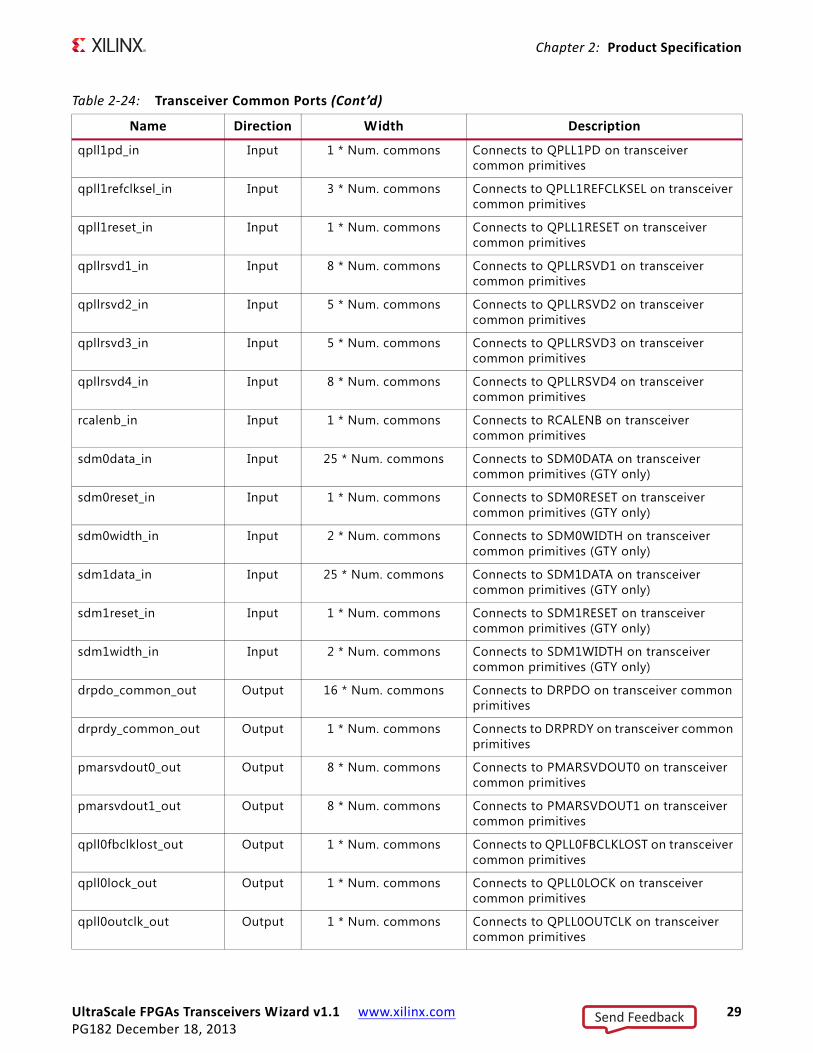
qpll0fbclklost_out Output 1 * Num. commons Connects to QPLL0FBCLKLOST on transceiver common primitives
qpll0lock_out Output 1 * Num. commons Connects to QPLL0LOCK on transceiver common primitives
qpll0outclk_out Output 1 * Num. commons Connects to QPLL0OUTCLK on transceiver common primitives
Table 2‐24: Transceiver Common Ports (Cont’d)
Name Direction Width Description
Send Feedback
UltraScale FPGAs Transceivers Wizard v1.1 www.xilinx.com 30PG182 December 18, 2013
Chapter 2: Product Specification
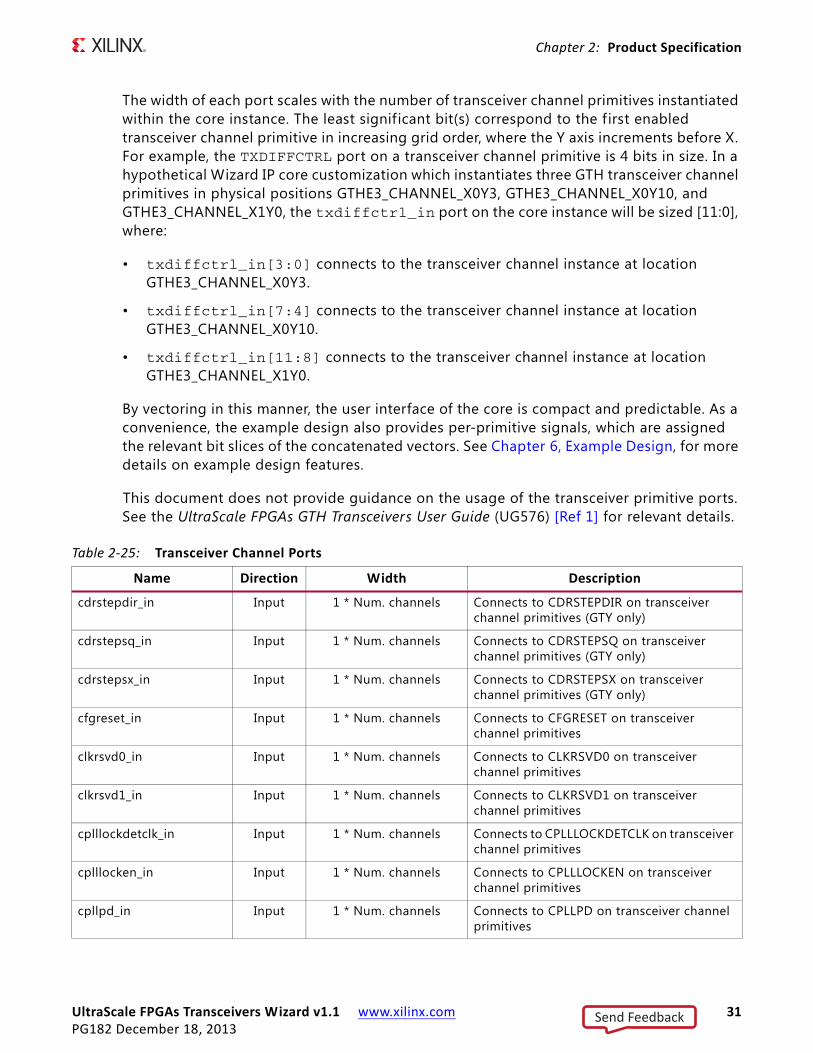
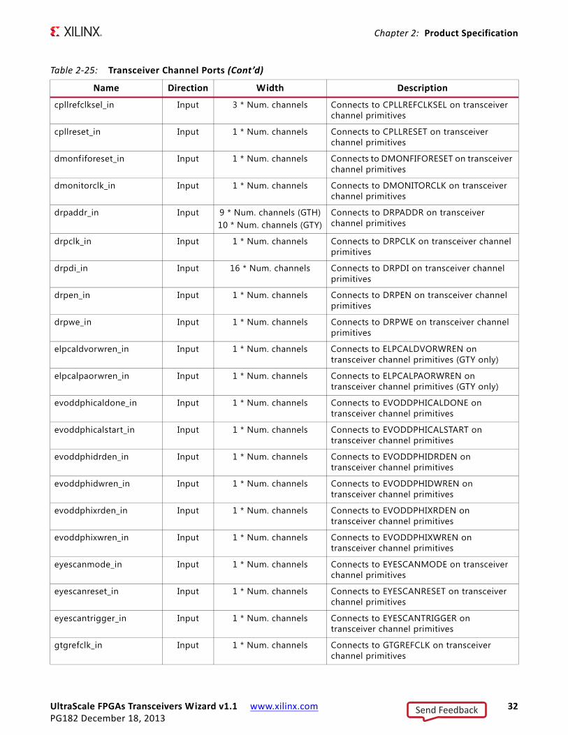
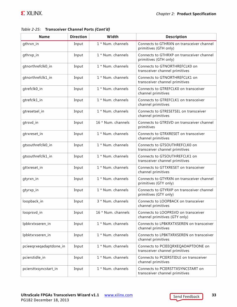
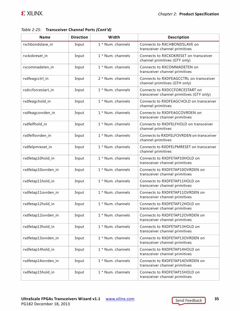
Transceiver Channel Ports
A subset of the ports described in Table 2-25 is present on the Wizard core instance. These ports connect through the core hierarchy to the corresponding transceiver channel primitive ports. Because only a subset is required for a given core customization, most are not exposed as ports on the core interface by default. See Chapter 4, Customizing and Generating the Core, for details on optional port enablement.
qpll0outrefclk_out Output 1 * Num. commons Connects to QPLL0OUTREFCLK on transceiver common primitives
qpll0refclklost_out Output 1 * Num. commons Connects to QPLL0REFCLKLOST on transceiver common primitives
qpll1fbclklost_out Output 1 * Num. commons Connects to QPLL1FBCLKLOST on transceiver common primitives
qpll1lock_out Output 1 * Num. commons Connects to QPLL1LOCK on transceiver common primitives
qpll1outclk_out Output 1 * Num. commons Connects to QPLL1OUTCLK on transceiver common primitives
qpll1outrefclk_out Output 1 * Num. commons Connects to QPLL1OUTREFCLK on transceiver common primitives
qpll1refclklost_out Output 1 * Num. commons Connects to QPLL1REFCLKLOST on transceiver common primitives
qplldmonitor0_out Output 8 * Num. commons Connects to QPLLDMONITOR0 on transceiver common primitives
qplldmonitor1_out Output 8 * Num. commons Connects to QPLLDMONITOR1 on transceiver common primitives
refclkoutmonitor0_out Output 1 * Num. commons Connects to REFCLKOUTMONITOR0 on transceiver common primitives
refclkoutmonitor1_out Output 1 * Num. commons Connects to REFCLKOUTMONITOR1 on transceiver common primitives
rxrecclk0_sel_out Output 2 * Num. commons Connects to RXRECCLK0_SEL on transceiver common primitives
rxrecclk1_sel_out Output 2 * Num. commons Connects to RXRECCLK1_SEL on transceiver common primitives
sdm0finalout_out Output 4 * Num. commons Connects to SDM0FINALOUT on transceiver common primitives (GTY only)
sdm0testdata_out Output 15 * Num. commons Connects to SDM0TESTDATA on transceiver common primitives (GTY only)
sdm1finalout_out Output 4 * Num. commons Connects to SDM1FINALOUT on transceiver common primitives (GTY only)
sdm1testdata_out Output 15 * Num. commons Connects to SDM1TESTDATA on transceiver common primitives (GTY only)
Table 2‐24: Transceiver Common Ports (Cont’d)
Name Direction Width Description
Send Feedback
UltraScale FPGAs Transceivers Wizard v1.1 www.xilinx.com 31PG182 December 18, 2013
Chapter 2: Product Specification
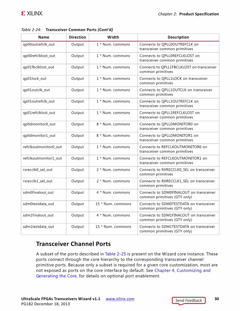
The width of each port scales with the number of transceiver channel primitives instantiated within the core instance. The least significant bit(s) correspond to the f irst enabled transceiver channel primitive in increasing grid order, where the Y axis increments before X. For example, the TXDIFFCTRL port on a transceiver channel primitive is 4 bits in size. In a hypothetical Wizard IP core customization which instantiates three GTH transceiver channel primitives in physical positions GTHE3_CHANNEL_X0Y3, GTHE3_CHANNEL_X0Y10, and GTHE3_CHANNEL_X1Y0, the txdiffctrl_in port on the core instance will be sized [11:0], where:
• txdiffctrl_in[3:0] connects to the transceiver channel instance at location GTHE3_CHANNEL_X0Y3.
• txdiffctrl_in[7:4] connects to the transceiver channel instance at location GTHE3_CHANNEL_X0Y10.
• txdiffctrl_in[11:8] connects to the transceiver channel instance at location GTHE3_CHANNEL_X1Y0.
By vectoring in this manner, the user interface of the core is compact and predictable. As a convenience, the example design also provides per-primitive signals, which are assigned the relevant bit slices of the concatenated vectors. See Chapter 6, Example Design, for more details on example design features.
This document does not provide guidance on the usage of the transceiver primitive ports. See the UltraScale FPGAs GTH Transceivers User Guide (UG576) [Ref 1] for relevant details.
Table 2‐25: Transceiver Channel Ports
Name Direction Width Description
cdrstepdir_in Input 1 * Num. channels Connects to CDRSTEPDIR on transceiver channel primitives (GTY only)
cdrstepsq_in Input 1 * Num. channels Connects to CDRSTEPSQ on transceiver channel primitives (GTY only)
cdrstepsx_in Input 1 * Num. channels Connects to CDRSTEPSX on transceiver channel primitives (GTY only)
cfgreset_in Input 1 * Num. channels Connects to CFGRESET on transceiver channel primitives
clkrsvd0_in Input 1 * Num. channels Connects to CLKRSVD0 on transceiver channel primitives
clkrsvd1_in Input 1 * Num. channels Connects to CLKRSVD1 on transceiver channel primitives
cplllockdetclk_in Input 1 * Num. channels Connects to CPLLLOCKDETCLK on transceiver channel primitives
cplllocken_in Input 1 * Num. channels Connects to CPLLLOCKEN on transceiver channel primitives
cpllpd_in Input 1 * Num. channels Connects to CPLLPD on transceiver channel primitives
Send Feedback
UltraScale FPGAs Transceivers Wizard v1.1 www.xilinx.com 32PG182 December 18, 2013
Chapter 2: Product Specification
cpllrefclksel_in Input 3 * Num. channels Connects to CPLLREFCLKSEL on transceiver channel primitives
cpllreset_in Input 1 * Num. channels Connects to CPLLRESET on transceiver channel primitives
dmonfiforeset_in Input 1 * Num. channels Connects to DMONFIFORESET on transceiver channel primitives
dmonitorclk_in Input 1 * Num. channels Connects to DMONITORCLK on transceiver channel primitives
drpaddr_in Input 9 * Num. channels (GTH)10 * Num. channels (GTY)
Connects to DRPADDR on transceiver channel primitives
drpclk_in Input 1 * Num. channels Connects to DRPCLK on transceiver channel primitives
drpdi_in Input 16 * Num. channels Connects to DRPDI on transceiver channel primitives
drpen_in Input 1 * Num. channels Connects to DRPEN on transceiver channel primitives
drpwe_in Input 1 * Num. channels Connects to DRPWE on transceiver channel primitives
elpcaldvorwren_in Input 1 * Num. channels Connects to ELPCALDVORWREN on transceiver channel primitives (GTY only)
elpcalpaorwren_in Input 1 * Num. channels Connects to ELPCALPAORWREN on transceiver channel primitives (GTY only)
evoddphicaldone_in Input 1 * Num. channels Connects to EVODDPHICALDONE on transceiver channel primitives
evoddphicalstart_in Input 1 * Num. channels Connects to EVODDPHICALSTART on transceiver channel primitives
evoddphidrden_in Input 1 * Num. channels Connects to EVODDPHIDRDEN on transceiver channel primitives
evoddphidwren_in Input 1 * Num. channels Connects to EVODDPHIDWREN on transceiver channel primitives
evoddphixrden_in Input 1 * Num. channels Connects to EVODDPHIXRDEN on transceiver channel primitives
evoddphixwren_in Input 1 * Num. channels Connects to EVODDPHIXWREN on transceiver channel primitives
eyescanmode_in Input 1 * Num. channels Connects to EYESCANMODE on transceiver channel primitives
eyescanreset_in Input 1 * Num. channels Connects to EYESCANRESET on transceiver channel primitives
eyescantrigger_in Input 1 * Num. channels Connects to EYESCANTRIGGER on transceiver channel primitives
gtgrefclk_in Input 1 * Num. channels Connects to GTGREFCLK on transceiver channel primitives
Table 2‐25: Transceiver Channel Ports (Cont’d)
Name Direction Width Description
Send Feedback
UltraScale FPGAs Transceivers Wizard v1.1 www.xilinx.com 33PG182 December 18, 2013
Chapter 2: Product Specification
gthrxn_in Input 1 * Num. channels Connects to GTHRXN on transceiver channel primitives (GTH only)
gthrxp_in Input 1 * Num. channels Connects to GTHRXP on transceiver channel primitives (GTH only)
gtnorthrefclk0_in Input 1 * Num. channels Connects to GTNORTHREFCLK0 on transceiver channel primitives
gtnorthrefclk1_in Input 1 * Num. channels Connects to GTNORTHREFCLK1 on transceiver channel primitives
gtrefclk0_in Input 1 * Num. channels Connects to GTREFCLK0 on transceiver channel primitives
gtrefclk1_in Input 1 * Num. channels Connects to GTREFCLK1 on transceiver channel primitives
gtresetsel_in Input 1 * Num. channels Connects to GTRESETSEL on transceiver channel primitives
gtrsvd_in Input 16 * Num. channels Connects to GTRSVD on transceiver channel primitives
gtrxreset_in Input 1 * Num. channels Connects to GTRXRESET on transceiver channel primitives
gtsouthrefclk0_in Input 1 * Num. channels Connects to GTSOUTHREFCLK0 on transceiver channel primitives
gtsouthrefclk1_in Input 1 * Num. channels Connects to GTSOUTHREFCLK1 on transceiver channel primitives
gttxreset_in Input 1 * Num. channels Connects to GTTXRESET on transceiver channel primitives
gtyrxn_in Input 1 * Num. channels Connects to GTYRXN on transceiver channel primitives (GTY only)
gtyrxp_in Input 1 * Num. channels Connects to GTYRXP on transceiver channel primitives (GTY only)
loopback_in Input 3 * Num. channels Connects to LOOPBACK on transceiver channel primitives
looprsvd_in Input 16 * Num. channels Connects to LOOPRSVD on transceiver channel primitives (GTY only)
lpbkrxtxseren_in Input 1 * Num. channels Connects to LPBKRXTXSEREN on transceiver channel primitives
lpbktxrxseren_in Input 1 * Num. channels Connects to LPBKTXRXSEREN on transceiver channel primitives
pcieeqrxeqadaptdone_in Input 1 * Num. channels Connects to PCIEEQRXEQADAPTDONE on transceiver channel primitives
pcierstidle_in Input 1 * Num. channels Connects to PCIERSTIDLE on transceiver channel primitives
pciersttxsyncstart_in Input 1 * Num. channels Connects to PCIERSTTXSYNCSTART on transceiver channel primitives
Table 2‐25: Transceiver Channel Ports (Cont’d)
Name Direction Width Description
Send Feedback

UltraScale FPGAs Transceivers Wizard v1.1 www.xilinx.com 34PG182 December 18, 2013
Chapter 2: Product Specification
pcieuserratedone_in Input 1 * Num. channels Connects to PCIEUSERRATEDONE on transceiver channel primitives
pcsrsvdin_in Input 16 * Num. channels Connects to PCSRSVDIN on transceiver channel primitives
pcsrsvdin2_in Input 5 * Num. channels Connects to PCSRSVDIN2 on transceiver channel primitives
pmarsvdin_in Input 5 * Num. channels Connects to PMARSVDIN on transceiver channel primitives
qpll0clk_in Input 1 * Num. channels Connects to QPLL0CLK on transceiver channel primitives
qpll0refclk_in Input 1 * Num. channels Connects to QPLL0REFCLK on transceiver channel primitives
qpll1clk_in Input 1 * Num. channels Connects to QPLL1CLK on transceiver channel primitives
qpll1refclk_in Input 1 * Num. channels Connects to QPLL1REFCLK on transceiver channel primitives
resetovrd_in Input 1 * Num. channels Connects to RESETOVRD on transceiver channel primitives
rstclkentx_in Input 1 * Num. channels Connects to RSTCLKENTX on transceiver channel primitives
rx8b10ben_in Input 1 * Num. channels Connects to RX8B10BEN on transceiver channel primitives
rxbufreset_in Input 1 * Num. channels Connects to RXBUFRESET on transceiver channel primitives
rxcdrfreqreset_in Input 1 * Num. channels Connects to RXCDRFREQRESET on transceiver channel primitives
rxcdrhold_in Input 1 * Num. channels Connects to RXCDRHOLD on transceiver channel primitives
rxcdrovrden_in Input 1 * Num. channels Connects to RXCDROVRDEN on transceiver channel primitives
rxcdrreset_in Input 1 * Num. channels Connects to RXCDRRESET on transceiver channel primitives
rxcdrresetrsv_in Input 1 * Num. channels Connects to RXCDRRESETRSV on transceiver channel primitives
rxchbonden_in Input 1 * Num. channels Connects to RXCHBONDEN on transceiver channel primitives
rxchbondi_in Input 5 * Num. channels Connects to RXCHBONDI on transceiver channel primitives
rxchbondlevel_in Input 3 * Num. channels Connects to RXCHBONDLEVEL on transceiver channel primitives
rxchbondmaster_in Input 1 * Num. channels Connects to RXCHBONDMASTER on transceiver channel primitives
Table 2‐25: Transceiver Channel Ports (Cont’d)
Name Direction Width Description
Send Feedback
UltraScale FPGAs Transceivers Wizard v1.1 www.xilinx.com 35PG182 December 18, 2013
Chapter 2: Product Specification
rxchbondslave_in Input 1 * Num. channels Connects to RXCHBONDSLAVE on transceiver channel primitives
rxckokreset_in Input 1 * Num. channels Connects to RXCKOKRESET on transceiver channel primitives (GTY only)
rxcommadeten_in Input 1 * Num. channels Connects to RXCOMMADETEN on transceiver channel primitives
rxdfeagcctrl_in Input 2 * Num. channels Connects to RXDFEAGCCTRL on transceiver channel primitives (GTH only)
rxdccforcestart_in Input 1 * Num. channels Connects to RXDCCFORCESTART on transceiver channel primitives (GTY only)
rxdfeagchold_in Input 1 * Num. channels Connects to RXDFEAGCHOLD on transceiver channel primitives
rxdfeagcovrden_in Input 1 * Num. channels Connects to RXDFEAGCOVRDEN on transceiver channel primitives
rxdfelfhold_in Input 1 * Num. channels Connects to RXDFELFHOLD on transceiver channel primitives
rxdfelfovrden_in Input 1 * Num. channels Connects to RXDFELFOVRDEN on transceiver channel primitives
rxdfelpmreset_in Input 1 * Num. channels Connects to RXDFELPMRESET on transceiver channel primitives
rxdfetap10hold_in Input 1 * Num. channels Connects to RXDFETAP10HOLD on transceiver channel primitives
rxdfetap10ovrden_in Input 1 * Num. channels Connects to RXDFETAP10OVRDEN on transceiver channel primitives
rxdfetap11hold_in Input 1 * Num. channels Connects to RXDFETAP11HOLD on transceiver channel primitives
rxdfetap11ovrden_in Input 1 * Num. channels Connects to RXDFETAP11OVRDEN on transceiver channel primitives
rxdfetap12hold_in Input 1 * Num. channels Connects to RXDFETAP12HOLD on transceiver channel primitives
rxdfetap12ovrden_in Input 1 * Num. channels Connects to RXDFETAP12OVRDEN on transceiver channel primitives
rxdfetap13hold_in Input 1 * Num. channels Connects to RXDFETAP13HOLD on transceiver channel primitives
rxdfetap13ovrden_in Input 1 * Num. channels Connects to RXDFETAP13OVRDEN on transceiver channel primitives
rxdfetap14hold_in Input 1 * Num. channels Connects to RXDFETAP14HOLD on transceiver channel primitives
rxdfetap14ovrden_in Input 1 * Num. channels Connects to RXDFETAP14OVRDEN on transceiver channel primitives
rxdfetap15hold_in Input 1 * Num. channels Connects to RXDFETAP15HOLD on transceiver channel primitives
Table 2‐25: Transceiver Channel Ports (Cont’d)
Name Direction Width Description
Send Feedback
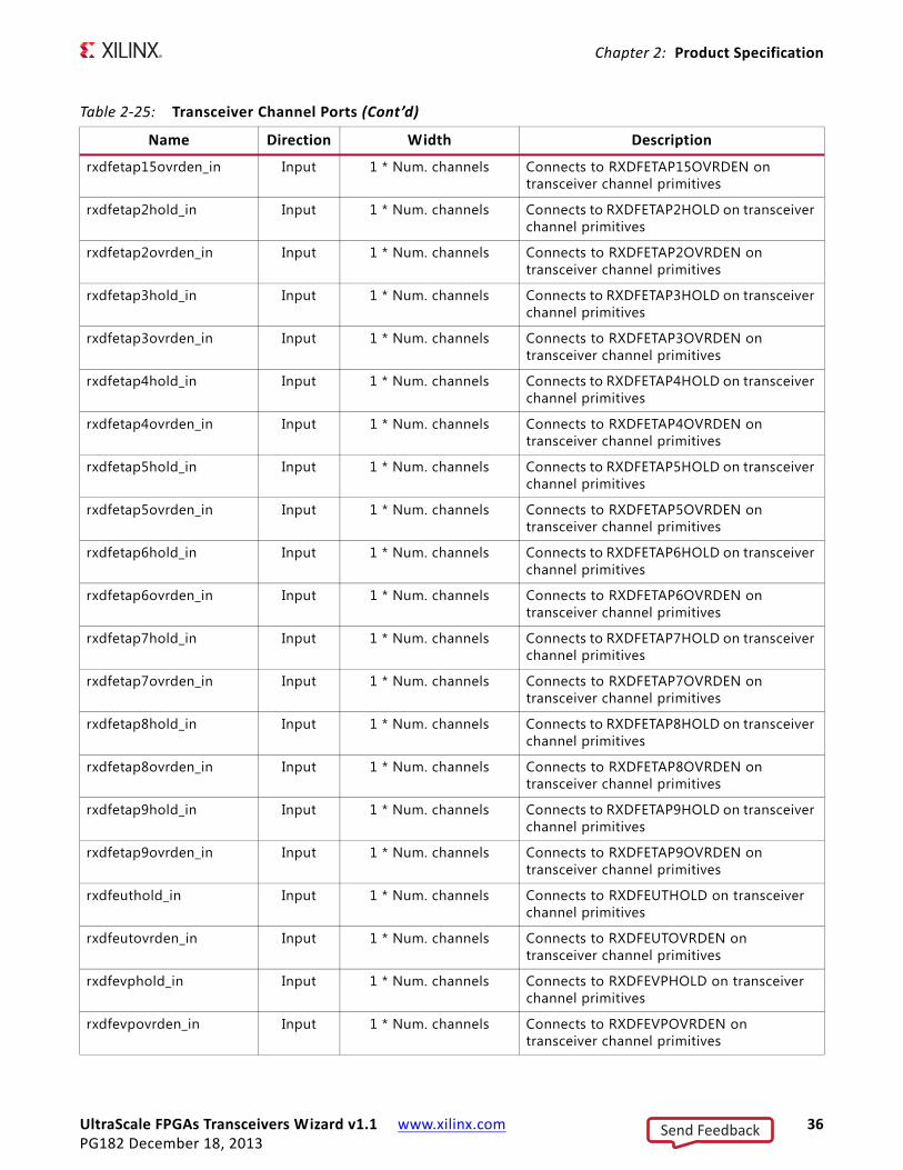
UltraScale FPGAs Transceivers Wizard v1.1 www.xilinx.com 36PG182 December 18, 2013
Chapter 2: Product Specification
rxdfetap15ovrden_in Input 1 * Num. channels Connects to RXDFETAP15OVRDEN on transceiver channel primitives
rxdfetap2hold_in Input 1 * Num. channels Connects to RXDFETAP2HOLD on transceiver channel primitives
rxdfetap2ovrden_in Input 1 * Num. channels Connects to RXDFETAP2OVRDEN on transceiver channel primitives
rxdfetap3hold_in Input 1 * Num. channels Connects to RXDFETAP3HOLD on transceiver channel primitives
rxdfetap3ovrden_in Input 1 * Num. channels Connects to RXDFETAP3OVRDEN on transceiver channel primitives
rxdfetap4hold_in Input 1 * Num. channels Connects to RXDFETAP4HOLD on transceiver channel primitives
rxdfetap4ovrden_in Input 1 * Num. channels Connects to RXDFETAP4OVRDEN on transceiver channel primitives
rxdfetap5hold_in Input 1 * Num. channels Connects to RXDFETAP5HOLD on transceiver channel primitives
rxdfetap5ovrden_in Input 1 * Num. channels Connects to RXDFETAP5OVRDEN on transceiver channel primitives
rxdfetap6hold_in Input 1 * Num. channels Connects to RXDFETAP6HOLD on transceiver channel primitives
rxdfetap6ovrden_in Input 1 * Num. channels Connects to RXDFETAP6OVRDEN on transceiver channel primitives
rxdfetap7hold_in Input 1 * Num. channels Connects to RXDFETAP7HOLD on transceiver channel primitives
rxdfetap7ovrden_in Input 1 * Num. channels Connects to RXDFETAP7OVRDEN on transceiver channel primitives
rxdfetap8hold_in Input 1 * Num. channels Connects to RXDFETAP8HOLD on transceiver channel primitives
rxdfetap8ovrden_in Input 1 * Num. channels Connects to RXDFETAP8OVRDEN on transceiver channel primitives
rxdfetap9hold_in Input 1 * Num. channels Connects to RXDFETAP9HOLD on transceiver channel primitives
rxdfetap9ovrden_in Input 1 * Num. channels Connects to RXDFETAP9OVRDEN on transceiver channel primitives
rxdfeuthold_in Input 1 * Num. channels Connects to RXDFEUTHOLD on transceiver channel primitives
rxdfeutovrden_in Input 1 * Num. channels Connects to RXDFEUTOVRDEN on transceiver channel primitives
rxdfevphold_in Input 1 * Num. channels Connects to RXDFEVPHOLD on transceiver channel primitives
rxdfevpovrden_in Input 1 * Num. channels Connects to RXDFEVPOVRDEN on transceiver channel primitives
Table 2‐25: Transceiver Channel Ports (Cont’d)
Name Direction Width Description
Send Feedback
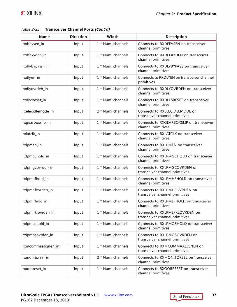
UltraScale FPGAs Transceivers Wizard v1.1 www.xilinx.com 37PG182 December 18, 2013
Chapter 2: Product Specification
rxdfevsen_in Input 1 * Num. channels Connects to RXDFEVSEN on transceiver channel primitives
rxdfexyden_in Input 1 * Num. channels Connects to RXDFEXYDEN on transceiver channel primitives
rxdlybypass_in Input 1 * Num. channels Connects to RXDLYBYPASS on transceiver channel primitives
rxdlyen_in Input 1 * Num. channels Connects to RXDLYEN on transceiver channel primitives
rxdlyovrden_in Input 1 * Num. channels Connects to RXDLYOVRDEN on transceiver channel primitives
rxdlysreset_in Input 1 * Num. channels Connects to RXDLYSRESET on transceiver channel primitives
rxelecidlemode_in Input 2 * Num. channels Connects to RXELECIDLEMODE on transceiver channel primitives
rxgearboxslip_in Input 1 * Num. channels Connects to RXGEARBOXSLIP on transceiver channel primitives
rxlatclk_in Input 1 * Num. channels Connects to RXLATCLK on transceiver channel primitives
rxlpmen_in Input 1 * Num. channels Connects to RXLPMEN on transceiver channel primitives
rxlpmgchold_in Input 1 * Num. channels Connects to RXLPMGCHOLD on transceiver channel primitives
rxlpmgcovrden_in Input 1 * Num. channels Connects to RXLPMGCOVRDEN on transceiver channel primitives
rxlpmhfhold_in Input 1 * Num. channels Connects to RXLPMHFHOLD on transceiver channel primitives
rxlpmhfovrden_in Input 1 * Num. channels Connects to RXLPMHFOVRDEN on transceiver channel primitives
rxlpmlfhold_in Input 1 * Num. channels Connects to RXLPMLFHOLD on transceiver channel primitives
rxlpmlfklovrden_in Input 1 * Num. channels Connects to RXLPMLFKLOVRDEN on transceiver channel primitives
rxlpmoshold_in Input 1 * Num. channels Connects to RXLPMOSHOLD on transceiver channel primitives
rxlpmosovrden_in Input 1 * Num. channels Connects to RXLPMOSOVRDEN on transceiver channel primitives
rxmcommaalignen_in Input 1 * Num. channels Connects to RXMCOMMAALIGNEN on transceiver channel primitives
rxmonitorsel_in Input 2 * Num. channels Connects to RXMONITORSEL on transceiver channel primitives
rxoobreset_in Input 1 * Num. channels Connects to RXOOBRESET on transceiver channel primitives
Table 2‐25: Transceiver Channel Ports (Cont’d)
Name Direction Width Description
Send Feedback
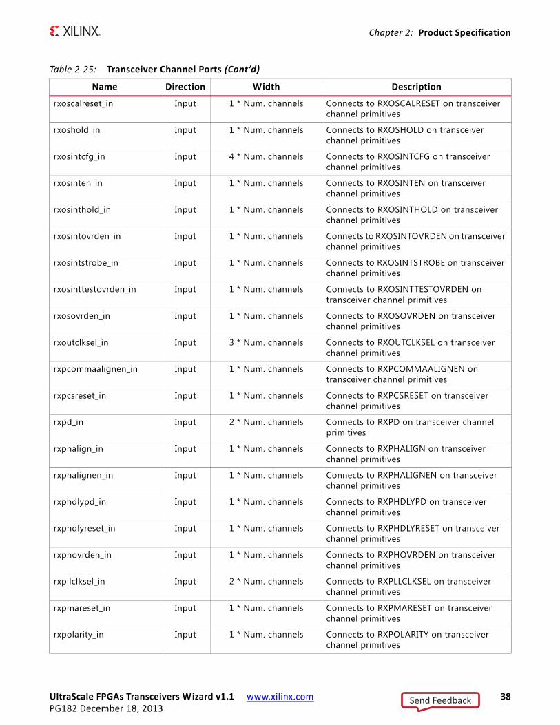
UltraScale FPGAs Transceivers Wizard v1.1 www.xilinx.com 38PG182 December 18, 2013
Chapter 2: Product Specification
rxoscalreset_in Input 1 * Num. channels Connects to RXOSCALRESET on transceiver channel primitives
rxoshold_in Input 1 * Num. channels Connects to RXOSHOLD on transceiver channel primitives
rxosintcfg_in Input 4 * Num. channels Connects to RXOSINTCFG on transceiver channel primitives
rxosinten_in Input 1 * Num. channels Connects to RXOSINTEN on transceiver channel primitives
rxosinthold_in Input 1 * Num. channels Connects to RXOSINTHOLD on transceiver channel primitives
rxosintovrden_in Input 1 * Num. channels Connects to RXOSINTOVRDEN on transceiver channel primitives
rxosintstrobe_in Input 1 * Num. channels Connects to RXOSINTSTROBE on transceiver channel primitives
rxosinttestovrden_in Input 1 * Num. channels Connects to RXOSINTTESTOVRDEN on transceiver channel primitives
rxosovrden_in Input 1 * Num. channels Connects to RXOSOVRDEN on transceiver channel primitives
rxoutclksel_in Input 3 * Num. channels Connects to RXOUTCLKSEL on transceiver channel primitives
rxpcommaalignen_in Input 1 * Num. channels Connects to RXPCOMMAALIGNEN on transceiver channel primitives
rxpcsreset_in Input 1 * Num. channels Connects to RXPCSRESET on transceiver channel primitives
rxpd_in Input 2 * Num. channels Connects to RXPD on transceiver channel primitives
rxphalign_in Input 1 * Num. channels Connects to RXPHALIGN on transceiver channel primitives
rxphalignen_in Input 1 * Num. channels Connects to RXPHALIGNEN on transceiver channel primitives
rxphdlypd_in Input 1 * Num. channels Connects to RXPHDLYPD on transceiver channel primitives
rxphdlyreset_in Input 1 * Num. channels Connects to RXPHDLYRESET on transceiver channel primitives
rxphovrden_in Input 1 * Num. channels Connects to RXPHOVRDEN on transceiver channel primitives
rxpllclksel_in Input 2 * Num. channels Connects to RXPLLCLKSEL on transceiver channel primitives
rxpmareset_in Input 1 * Num. channels Connects to RXPMARESET on transceiver channel primitives
rxpolarity_in Input 1 * Num. channels Connects to RXPOLARITY on transceiver channel primitives
Table 2‐25: Transceiver Channel Ports (Cont’d)
Name Direction Width Description
Send Feedback
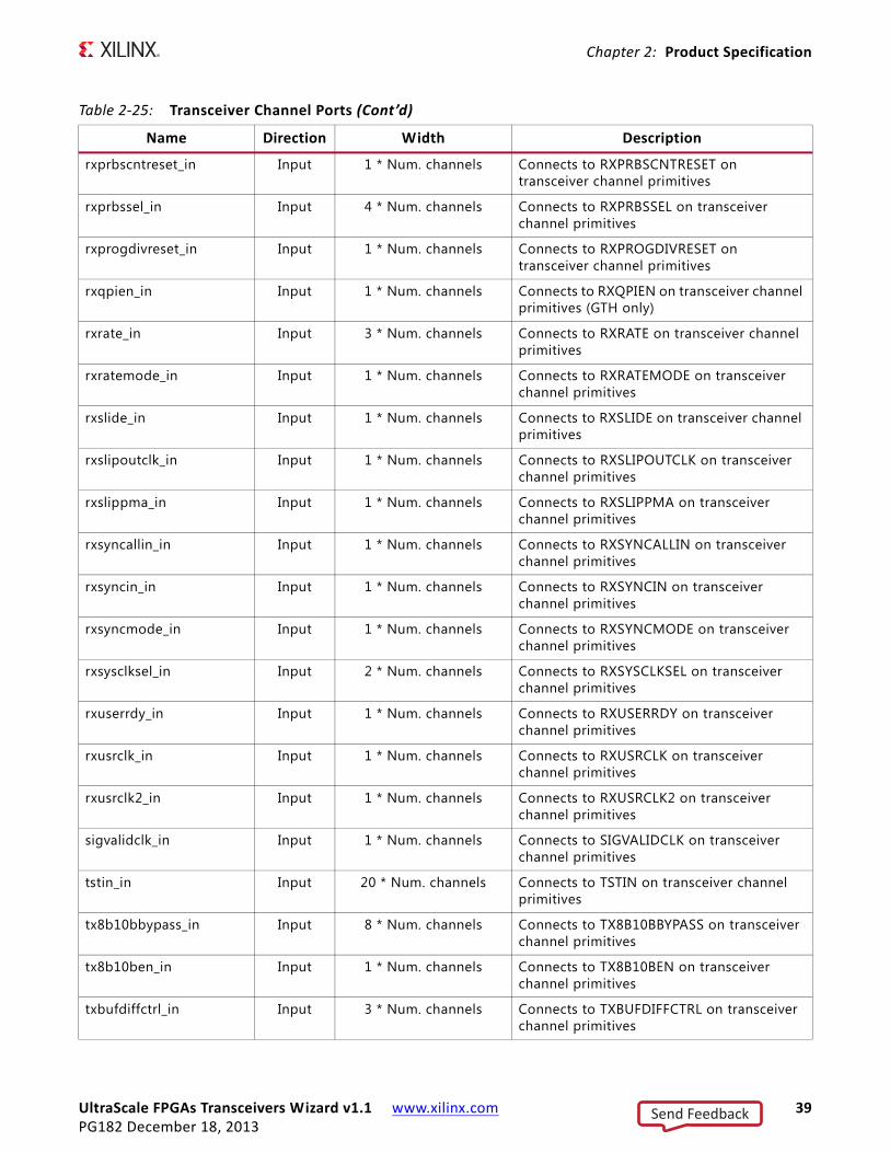
UltraScale FPGAs Transceivers Wizard v1.1 www.xilinx.com 39PG182 December 18, 2013
Chapter 2: Product Specification
rxprbscntreset_in Input 1 * Num. channels Connects to RXPRBSCNTRESET on transceiver channel primitives
rxprbssel_in Input 4 * Num. channels Connects to RXPRBSSEL on transceiver channel primitives
rxprogdivreset_in Input 1 * Num. channels Connects to RXPROGDIVRESET on transceiver channel primitives
rxqpien_in Input 1 * Num. channels Connects to RXQPIEN on transceiver channel primitives (GTH only)
rxrate_in Input 3 * Num. channels Connects to RXRATE on transceiver channel primitives
rxratemode_in Input 1 * Num. channels Connects to RXRATEMODE on transceiver channel primitives
rxslide_in Input 1 * Num. channels Connects to RXSLIDE on transceiver channel primitives
rxslipoutclk_in Input 1 * Num. channels Connects to RXSLIPOUTCLK on transceiver channel primitives
rxslippma_in Input 1 * Num. channels Connects to RXSLIPPMA on transceiver channel primitives
rxsyncallin_in Input 1 * Num. channels Connects to RXSYNCALLIN on transceiver channel primitives
rxsyncin_in Input 1 * Num. channels Connects to RXSYNCIN on transceiver channel primitives
rxsyncmode_in Input 1 * Num. channels Connects to RXSYNCMODE on transceiver channel primitives
rxsysclksel_in Input 2 * Num. channels Connects to RXSYSCLKSEL on transceiver channel primitives
rxuserrdy_in Input 1 * Num. channels Connects to RXUSERRDY on transceiver channel primitives
rxusrclk_in Input 1 * Num. channels Connects to RXUSRCLK on transceiver channel primitives
rxusrclk2_in Input 1 * Num. channels Connects to RXUSRCLK2 on transceiver channel primitives
sigvalidclk_in Input 1 * Num. channels Connects to SIGVALIDCLK on transceiver channel primitives
tstin_in Input 20 * Num. channels Connects to TSTIN on transceiver channel primitives
tx8b10bbypass_in Input 8 * Num. channels Connects to TX8B10BBYPASS on transceiver channel primitives
tx8b10ben_in Input 1 * Num. channels Connects to TX8B10BEN on transceiver channel primitives
txbufdiffctrl_in Input 3 * Num. channels Connects to TXBUFDIFFCTRL on transceiver channel primitives
Table 2‐25: Transceiver Channel Ports (Cont’d)
Name Direction Width Description
Send Feedback
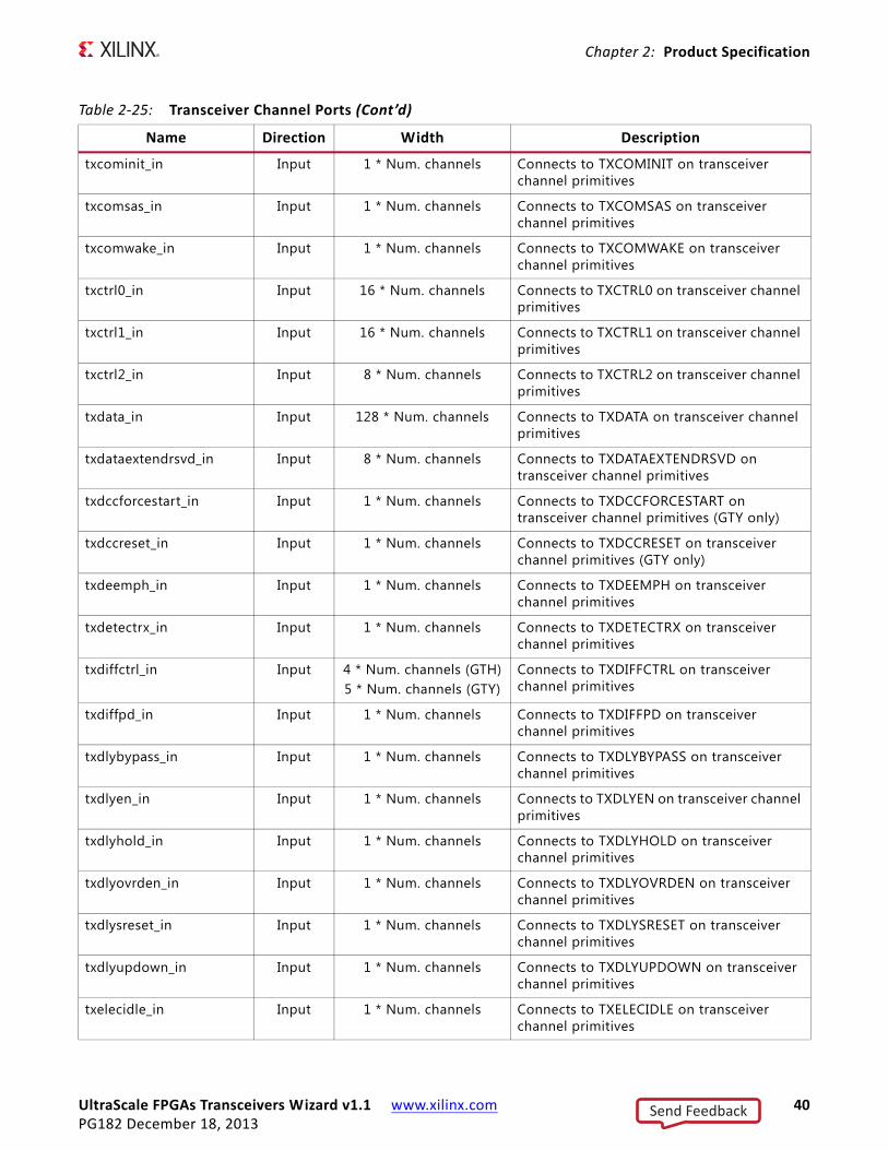
UltraScale FPGAs Transceivers Wizard v1.1 www.xilinx.com 40PG182 December 18, 2013
Chapter 2: Product Specification
txcominit_in Input 1 * Num. channels Connects to TXCOMINIT on transceiver channel primitives
txcomsas_in Input 1 * Num. channels Connects to TXCOMSAS on transceiver channel primitives
txcomwake_in Input 1 * Num. channels Connects to TXCOMWAKE on transceiver channel primitives
txctrl0_in Input 16 * Num. channels Connects to TXCTRL0 on transceiver channel primitives
txctrl1_in Input 16 * Num. channels Connects to TXCTRL1 on transceiver channel primitives
txctrl2_in Input 8 * Num. channels Connects to TXCTRL2 on transceiver channel primitives
txdata_in Input 128 * Num. channels Connects to TXDATA on transceiver channel primitives
txdataextendrsvd_in Input 8 * Num. channels Connects to TXDATAEXTENDRSVD on transceiver channel primitives
txdccforcestart_in Input 1 * Num. channels Connects to TXDCCFORCESTART on transceiver channel primitives (GTY only)
txdccreset_in Input 1 * Num. channels Connects to TXDCCRESET on transceiver channel primitives (GTY only)
txdeemph_in Input 1 * Num. channels Connects to TXDEEMPH on transceiver channel primitives
txdetectrx_in Input 1 * Num. channels Connects to TXDETECTRX on transceiver channel primitives
txdiffctrl_in Input 4 * Num. channels (GTH)5 * Num. channels (GTY)
Connects to TXDIFFCTRL on transceiver channel primitives
txdiffpd_in Input 1 * Num. channels Connects to TXDIFFPD on transceiver channel primitives
txdlybypass_in Input 1 * Num. channels Connects to TXDLYBYPASS on transceiver channel primitives
txdlyen_in Input 1 * Num. channels Connects to TXDLYEN on transceiver channel primitives
txdlyhold_in Input 1 * Num. channels Connects to TXDLYHOLD on transceiver channel primitives
txdlyovrden_in Input 1 * Num. channels Connects to TXDLYOVRDEN on transceiver channel primitives
txdlysreset_in Input 1 * Num. channels Connects to TXDLYSRESET on transceiver channel primitives
txdlyupdown_in Input 1 * Num. channels Connects to TXDLYUPDOWN on transceiver channel primitives
txelecidle_in Input 1 * Num. channels Connects to TXELECIDLE on transceiver channel primitives
Table 2‐25: Transceiver Channel Ports (Cont’d)
Name Direction Width Description
Send Feedback
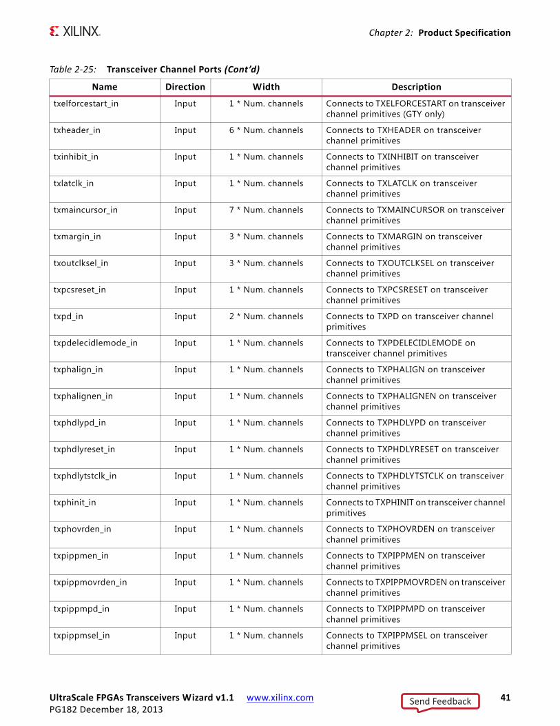
UltraScale FPGAs Transceivers Wizard v1.1 www.xilinx.com 41PG182 December 18, 2013
Chapter 2: Product Specification
txelforcestart_in Input 1 * Num. channels Connects to TXELFORCESTART on transceiver channel primitives (GTY only)
txheader_in Input 6 * Num. channels Connects to TXHEADER on transceiver channel primitives
txinhibit_in Input 1 * Num. channels Connects to TXINHIBIT on transceiver channel primitives
txlatclk_in Input 1 * Num. channels Connects to TXLATCLK on transceiver channel primitives
txmaincursor_in Input 7 * Num. channels Connects to TXMAINCURSOR on transceiver channel primitives
txmargin_in Input 3 * Num. channels Connects to TXMARGIN on transceiver channel primitives
txoutclksel_in Input 3 * Num. channels Connects to TXOUTCLKSEL on transceiver channel primitives
txpcsreset_in Input 1 * Num. channels Connects to TXPCSRESET on transceiver channel primitives
txpd_in Input 2 * Num. channels Connects to TXPD on transceiver channel primitives
txpdelecidlemode_in Input 1 * Num. channels Connects to TXPDELECIDLEMODE on transceiver channel primitives
txphalign_in Input 1 * Num. channels Connects to TXPHALIGN on transceiver channel primitives
txphalignen_in Input 1 * Num. channels Connects to TXPHALIGNEN on transceiver channel primitives
txphdlypd_in Input 1 * Num. channels Connects to TXPHDLYPD on transceiver channel primitives
txphdlyreset_in Input 1 * Num. channels Connects to TXPHDLYRESET on transceiver channel primitives
txphdlytstclk_in Input 1 * Num. channels Connects to TXPHDLYTSTCLK on transceiver channel primitives
txphinit_in Input 1 * Num. channels Connects to TXPHINIT on transceiver channel primitives
txphovrden_in Input 1 * Num. channels Connects to TXPHOVRDEN on transceiver channel primitives
txpippmen_in Input 1 * Num. channels Connects to TXPIPPMEN on transceiver channel primitives
txpippmovrden_in Input 1 * Num. channels Connects to TXPIPPMOVRDEN on transceiver channel primitives
txpippmpd_in Input 1 * Num. channels Connects to TXPIPPMPD on transceiver channel primitives
txpippmsel_in Input 1 * Num. channels Connects to TXPIPPMSEL on transceiver channel primitives
Table 2‐25: Transceiver Channel Ports (Cont’d)
Name Direction Width Description
Send Feedback
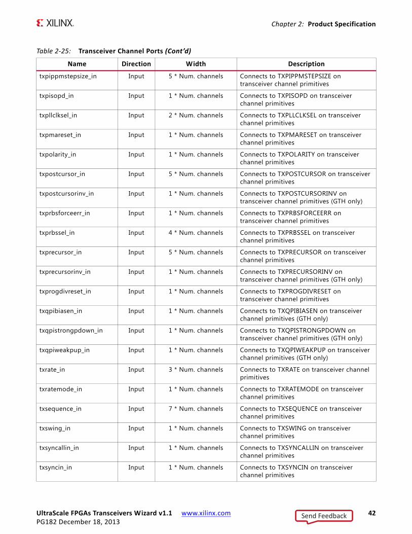
UltraScale FPGAs Transceivers Wizard v1.1 www.xilinx.com 42PG182 December 18, 2013
Chapter 2: Product Specification
txpippmstepsize_in Input 5 * Num. channels Connects to TXPIPPMSTEPSIZE on transceiver channel primitives
txpisopd_in Input 1 * Num. channels Connects to TXPISOPD on transceiver channel primitives
txpllclksel_in Input 2 * Num. channels Connects to TXPLLCLKSEL on transceiver channel primitives
txpmareset_in Input 1 * Num. channels Connects to TXPMARESET on transceiver channel primitives
txpolarity_in Input 1 * Num. channels Connects to TXPOLARITY on transceiver channel primitives
txpostcursor_in Input 5 * Num. channels Connects to TXPOSTCURSOR on transceiver channel primitives
txpostcursorinv_in Input 1 * Num. channels Connects to TXPOSTCURSORINV on transceiver channel primitives (GTH only)
txprbsforceerr_in Input 1 * Num. channels Connects to TXPRBSFORCEERR on transceiver channel primitives
txprbssel_in Input 4 * Num. channels Connects to TXPRBSSEL on transceiver channel primitives
txprecursor_in Input 5 * Num. channels Connects to TXPRECURSOR on transceiver channel primitives
txprecursorinv_in Input 1 * Num. channels Connects to TXPRECURSORINV on transceiver channel primitives (GTH only)
txprogdivreset_in Input 1 * Num. channels Connects to TXPROGDIVRESET on transceiver channel primitives
txqpibiasen_in Input 1 * Num. channels Connects to TXQPIBIASEN on transceiver channel primitives (GTH only)
txqpistrongpdown_in Input 1 * Num. channels Connects to TXQPISTRONGPDOWN on transceiver channel primitives (GTH only)
txqpiweakpup_in Input 1 * Num. channels Connects to TXQPIWEAKPUP on transceiver channel primitives (GTH only)
txrate_in Input 3 * Num. channels Connects to TXRATE on transceiver channel primitives
txratemode_in Input 1 * Num. channels Connects to TXRATEMODE on transceiver channel primitives
txsequence_in Input 7 * Num. channels Connects to TXSEQUENCE on transceiver channel primitives
txswing_in Input 1 * Num. channels Connects to TXSWING on transceiver channel primitives
txsyncallin_in Input 1 * Num. channels Connects to TXSYNCALLIN on transceiver channel primitives
txsyncin_in Input 1 * Num. channels Connects to TXSYNCIN on transceiver channel primitives
Table 2‐25: Transceiver Channel Ports (Cont’d)
Name Direction Width Description
Send Feedback
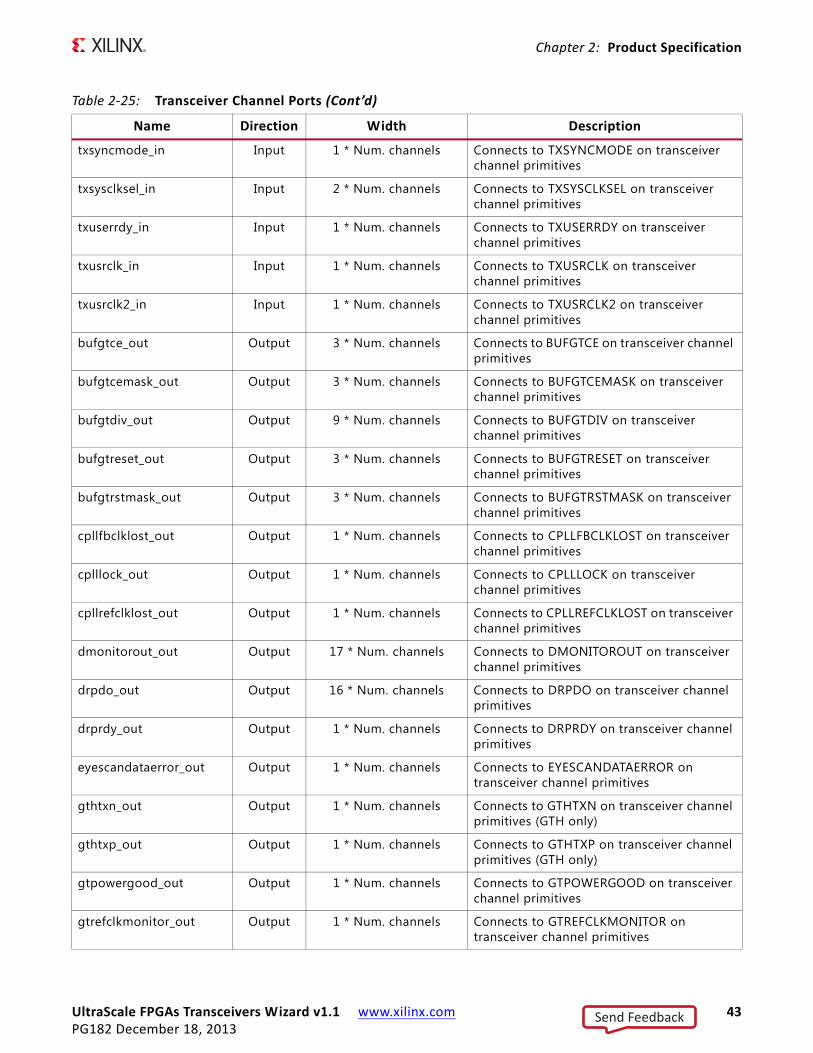
UltraScale FPGAs Transceivers Wizard v1.1 www.xilinx.com 43PG182 December 18, 2013
Chapter 2: Product Specification
txsyncmode_in Input 1 * Num. channels Connects to TXSYNCMODE on transceiver channel primitives
txsysclksel_in Input 2 * Num. channels Connects to TXSYSCLKSEL on transceiver channel primitives
txuserrdy_in Input 1 * Num. channels Connects to TXUSERRDY on transceiver channel primitives
txusrclk_in Input 1 * Num. channels Connects to TXUSRCLK on transceiver channel primitives
txusrclk2_in Input 1 * Num. channels Connects to TXUSRCLK2 on transceiver channel primitives
bufgtce_out Output 3 * Num. channels Connects to BUFGTCE on transceiver channel primitives
bufgtcemask_out Output 3 * Num. channels Connects to BUFGTCEMASK on transceiver channel primitives
bufgtdiv_out Output 9 * Num. channels Connects to BUFGTDIV on transceiver channel primitives
bufgtreset_out Output 3 * Num. channels Connects to BUFGTRESET on transceiver channel primitives
bufgtrstmask_out Output 3 * Num. channels Connects to BUFGTRSTMASK on transceiver channel primitives
cpllfbclklost_out Output 1 * Num. channels Connects to CPLLFBCLKLOST on transceiver channel primitives
cplllock_out Output 1 * Num. channels Connects to CPLLLOCK on transceiver channel primitives
cpllrefclklost_out Output 1 * Num. channels Connects to CPLLREFCLKLOST on transceiver channel primitives
dmonitorout_out Output 17 * Num. channels Connects to DMONITOROUT on transceiver channel primitives
drpdo_out Output 16 * Num. channels Connects to DRPDO on transceiver channel primitives
drprdy_out Output 1 * Num. channels Connects to DRPRDY on transceiver channel primitives
eyescandataerror_out Output 1 * Num. channels Connects to EYESCANDATAERROR on transceiver channel primitives
gthtxn_out Output 1 * Num. channels Connects to GTHTXN on transceiver channel primitives (GTH only)
gthtxp_out Output 1 * Num. channels Connects to GTHTXP on transceiver channel primitives (GTH only)
gtpowergood_out Output 1 * Num. channels Connects to GTPOWERGOOD on transceiver channel primitives
gtrefclkmonitor_out Output 1 * Num. channels Connects to GTREFCLKMONITOR on transceiver channel primitives
Table 2‐25: Transceiver Channel Ports (Cont’d)
Name Direction Width Description
Send Feedback
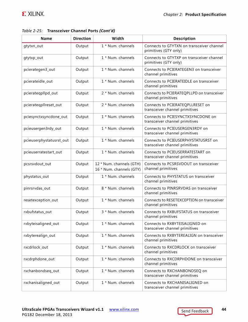
UltraScale FPGAs Transceivers Wizard v1.1 www.xilinx.com 44PG182 December 18, 2013
Chapter 2: Product Specification
gtytxn_out Output 1 * Num. channels Connects to GTYTXN on transceiver channel primitives (GTY only)
gtytxp_out Output 1 * Num. channels Connects to GTYTXP on transceiver channel primitives (GTY only)
pcierategen3_out Output 1 * Num. channels Connects to PCIERATEGEN3 on transceiver channel primitives
pcierateidle_out Output 1 * Num. channels Connects to PCIERATEIDLE on transceiver channel primitives
pcierateqpllpd_out Output 2 * Num. channels Connects to PCIERATEQPLLPD on transceiver channel primitives
pcierateqpllreset_out Output 2 * Num. channels Connects to PCIERATEQPLLRESET on transceiver channel primitives
pciesynctxsyncdone_out Output 1 * Num. channels Connects to PCIESYNCTXSYNCDONE on transceiver channel primitives
pcieusergen3rdy_out Output 1 * Num. channels Connects to PCIEUSERGEN3RDY on transceiver channel primitives
pcieuserphystatusrst_out Output 1 * Num. channels Connects to PCIEUSERPHYSTATUSRST on transceiver channel primitives
pcieuserratestart_out Output 1 * Num. channels Connects to PCIEUSERRATESTART on transceiver channel primitives
pcsrsvdout_out Output 12 * Num. channels (GTH)16 * Num. channels (GTY)
Connects to PCSRSVDOUT on transceiver channel primitives
phystatus_out Output 1 * Num. channels Connects to PHYSTATUS on transceiver channel primitives
pinrsrvdas_out Output 8 * Num. channels Connects to PINRSRVDAS on transceiver channel primitives
resetexception_out Output 1 * Num. channels Connects to RESETEXCEPTION on transceiver channel primitives
rxbufstatus_out Output 3 * Num. channels Connects to RXBUFSTATUS on transceiver channel primitives
rxbyteisaligned_out Output 1 * Num. channels Connects to RXBYTEISALIGNED on transceiver channel primitives
rxbyterealign_out Output 1 * Num. channels Connects to RXBYTEREALIGN on transceiver channel primitives
rxcdrlock_out Output 1 * Num. channels Connects to RXCDRLOCK on transceiver channel primitives
rxcdrphdone_out Output 1 * Num. channels Connects to RXCDRPHDONE on transceiver channel primitives
rxchanbondseq_out Output 1 * Num. channels Connects to RXCHANBONDSEQ on transceiver channel primitives
rxchanisaligned_out Output 1 * Num. channels Connects to RXCHANISALIGNED on transceiver channel primitives
Table 2‐25: Transceiver Channel Ports (Cont’d)
Name Direction Width Description
Send Feedback
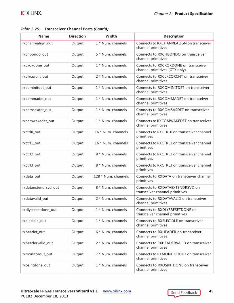
UltraScale FPGAs Transceivers Wizard v1.1 www.xilinx.com 45PG182 December 18, 2013
Chapter 2: Product Specification
rxchanrealign_out Output 1 * Num. channels Connects to RXCHANREALIGN on transceiver channel primitives
rxchbondo_out Output 5 * Num. channels Connects to RXCHBONDO on transceiver channel primitives
rxckokdone_out Output 1 * Num. channels Connects to RXCKOKDONE on transceiver channel primitives (GTY only)
rxclkcorcnt_out Output 2 * Num. channels Connects to RXCLKCORCNT on transceiver channel primitives
rxcominitdet_out Output 1 * Num. channels Connects to RXCOMINITDET on transceiver channel primitives
rxcommadet_out Output 1 * Num. channels Connects to RXCOMMADET on transceiver channel primitives
rxcomsasdet_out Output 1 * Num. channels Connects to RXCOMSASDET on transceiver channel primitives
rxcomwakedet_out Output 1 * Num. channels Connects to RXCOMWAKEDET on transceiver channel primitives
rxctrl0_out Output 16 * Num. channels Connects to RXCTRL0 on transceiver channel primitives
rxctrl1_out Output 16 * Num. channels Connects to RXCTRL1 on transceiver channel primitives
rxctrl2_out Output 8 * Num. channels Connects to RXCTRL2 on transceiver channel primitives
rxctrl3_out Output 8 * Num. channels Connects to RXCTRL3 on transceiver channel primitives
rxdata_out Output 128 * Num. channels Connects to RXDATA on transceiver channel primitives
rxdataextendrsvd_out Output 8 * Num. channels Connects to RXDATAEXTENDRSVD on transceiver channel primitives
rxdatavalid_out Output 2 * Num. channels Connects to RXDATAVALID on transceiver channel primitives
rxdlysresetdone_out Output 1 * Num. channels Connects to RXDLYSRESETDONE on transceiver channel primitives
rxelecidle_out Output 1 * Num. channels Connects to RXELECIDLE on transceiver channel primitives
rxheader_out Output 6 * Num. channels Connects to RXHEADER on transceiver channel primitives
rxheadervalid_out Output 2 * Num. channels Connects to RXHEADERVALID on transceiver channel primitives
rxmonitorout_out Output 7 * Num. channels Connects to RXMONITOROUT on transceiver channel primitives
rxosintdone_out Output 1 * Num. channels Connects to RXOSINTDONE on transceiver channel primitives
Table 2‐25: Transceiver Channel Ports (Cont’d)
Name Direction Width Description
Send Feedback
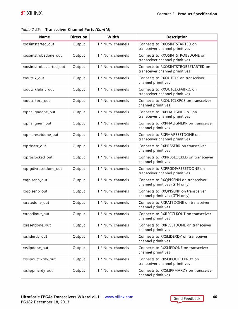
UltraScale FPGAs Transceivers Wizard v1.1 www.xilinx.com 46PG182 December 18, 2013
Chapter 2: Product Specification
rxosintstarted_out Output 1 * Num. channels Connects to RXOSINTSTARTED on transceiver channel primitives
rxosintstrobedone_out Output 1 * Num. channels Connects to RXOSINTSTROBEDONE on transceiver channel primitives
rxosintstrobestarted_out Output 1 * Num. channels Connects to RXOSINTSTROBESTARTED on transceiver channel primitives
rxoutclk_out Output 1 * Num. channels Connects to RXOUTCLK on transceiver channel primitives
rxoutclkfabric_out Output 1 * Num. channels Connects to RXOUTCLKFABRIC on transceiver channel primitives
rxoutclkpcs_out Output 1 * Num. channels Connects to RXOUTCLKPCS on transceiver channel primitives
rxphaligndone_out Output 1 * Num. channels Connects to RXPHALIGNDONE on transceiver channel primitives
rxphalignerr_out Output 1 * Num. channels Connects to RXPHALIGNERR on transceiver channel primitives
rxpmaresetdone_out Output 1 * Num. channels Connects to RXPMARESETDONE on transceiver channel primitives
rxprbserr_out Output 1 * Num. channels Connects to RXPRBSERR on transceiver channel primitives
rxprbslocked_out Output 1 * Num. channels Connects to RXPRBSLOCKED on transceiver channel primitives
rxprgdivresetdone_out Output 1 * Num. channels Connects to RXPRGDIVRESETDONE on transceiver channel primitives
rxqpisenn_out Output 1 * Num. channels Connects to RXQPISENN on transceiver channel primitives (GTH only)
rxqpisenp_out Output 1 * Num. channels Connects to RXQPISENP on transceiver channel primitives (GTH only)
rxratedone_out Output 1 * Num. channels Connects to RXRATEDONE on transceiver channel primitives
rxrecclkout_out Output 1 * Num. channels Connects to RXRECCLKOUT on transceiver channel primitives
rxresetdone_out Output 1 * Num. channels Connects to RXRESETDONE on transceiver channel primitives
rxsliderdy_out Output 1 * Num. channels Connects to RXSLIDERDY on transceiver channel primitives
rxslipdone_out Output 1 * Num. channels Connects to RXSLIPDONE on transceiver channel primitives
rxslipoutclkrdy_out Output 1 * Num. channels Connects to RXSLIPOUTCLKRDY on transceiver channel primitives
rxslippmardy_out Output 1 * Num. channels Connects to RXSLIPPMARDY on transceiver channel primitives
Table 2‐25: Transceiver Channel Ports (Cont’d)
Name Direction Width Description
Send Feedback
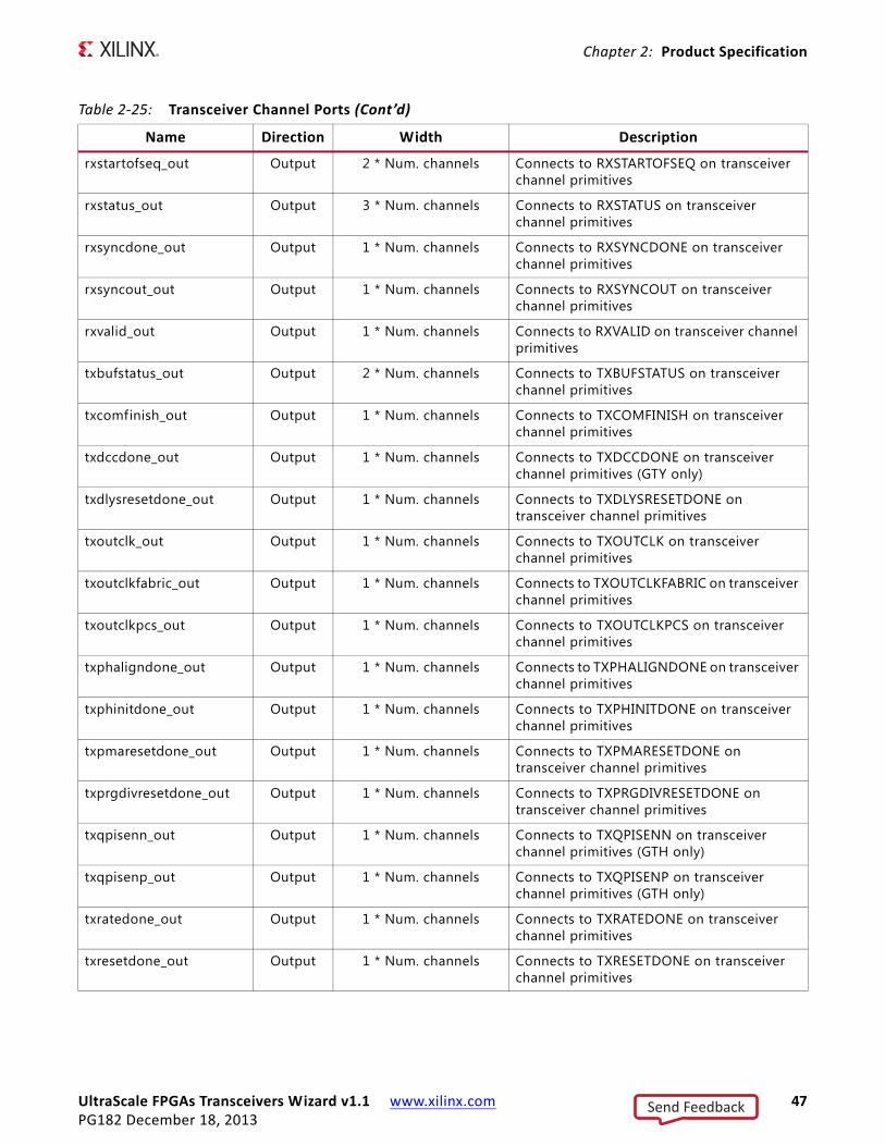
UltraScale FPGAs Transceivers Wizard v1.1 www.xilinx.com 47PG182 December 18, 2013
Chapter 2: Product Specification
rxstartofseq_out Output 2 * Num. channels Connects to RXSTARTOFSEQ on transceiver channel primitives
rxstatus_out Output 3 * Num. channels Connects to RXSTATUS on transceiver channel primitives
rxsyncdone_out Output 1 * Num. channels Connects to RXSYNCDONE on transceiver channel primitives
rxsyncout_out Output 1 * Num. channels Connects to RXSYNCOUT on transceiver channel primitives
rxvalid_out Output 1 * Num. channels Connects to RXVALID on transceiver channel primitives
txbufstatus_out Output 2 * Num. channels Connects to TXBUFSTATUS on transceiver channel primitives
txcomfinish_out Output 1 * Num. channels Connects to TXCOMFINISH on transceiver channel primitives
txdccdone_out Output 1 * Num. channels Connects to TXDCCDONE on transceiver channel primitives (GTY only)
txdlysresetdone_out Output 1 * Num. channels Connects to TXDLYSRESETDONE on transceiver channel primitives
txoutclk_out Output 1 * Num. channels Connects to TXOUTCLK on transceiver channel primitives
txoutclkfabric_out Output 1 * Num. channels Connects to TXOUTCLKFABRIC on transceiver channel primitives
txoutclkpcs_out Output 1 * Num. channels Connects to TXOUTCLKPCS on transceiver channel primitives
txphaligndone_out Output 1 * Num. channels Connects to TXPHALIGNDONE on transceiver channel primitives
txphinitdone_out Output 1 * Num. channels Connects to TXPHINITDONE on transceiver channel primitives
txpmaresetdone_out Output 1 * Num. channels Connects to TXPMARESETDONE on transceiver channel primitives
txprgdivresetdone_out Output 1 * Num. channels Connects to TXPRGDIVRESETDONE on transceiver channel primitives
txqpisenn_out Output 1 * Num. channels Connects to TXQPISENN on transceiver channel primitives (GTH only)
txqpisenp_out Output 1 * Num. channels Connects to TXQPISENP on transceiver channel primitives (GTH only)
txratedone_out Output 1 * Num. channels Connects to TXRATEDONE on transceiver channel primitives
txresetdone_out Output 1 * Num. channels Connects to TXRESETDONE on transceiver channel primitives
Table 2‐25: Transceiver Channel Ports (Cont’d)
Name Direction Width Description
Send Feedback
UltraScale FPGAs Transceivers Wizard v1.1 www.xilinx.com 48PG182 December 18, 2013
Chapter 2: Product Specification
txsyncdone_out Output 1 * Num. channels Connects to TXSYNCDONE on transceiver channel primitives
txsyncout_out Output 1 * Num. channels Connects to TXSYNCOUT on transceiver channel primitives
Table 2‐25: Transceiver Channel Ports (Cont’d)
Name Direction Width Description
Send Feedback
UltraScale FPGAs Transceivers Wizard v1.1 www.xilinx.com 49PG182 December 18, 2013
Chapter 3
Designing with the CoreThis chapter includes guidelines and additional information to facilitate designing with the UltraScale™ FPGAs Transceivers Wizard IP core.
General Design GuidelinesThe design guidelines for the Wizard core largely reflect those of the serial transceivers instantiated by the Wizard. It is important to understand the general usage and specif ic procedures that are required for correct operation of serial transceivers in your system. See the UltraScale FPGAs GTH Transceivers User Guide (UG576) [Ref 1] for details.
The Wizard provides a highly flexible Vivado® IDE-driven customization flow, which in addition to basic customization of transceiver use modes, also includes a physical resource site selection interface, an optional port enablement interface, and helper block location choices. The result is a core instance that addresses the specific needs of your application. As such, Wizard IP core instances do not require manual modif ication and should not be edited. Xilinx cannot guarantee timing, functionality, or support if modif ications are made to any output products of the generated core.
Designing with the Helper Blocks
The helper block modules provided with the Wizard simplify common or complex transceiver usage. Design and usage guidelines of these helper blocks are presented in the following sections.
Consider the benefits and drawbacks of each choice when deciding whether to locate each helper block within the core or in the example design. The primary benefits of locating a helper block within the core are a simpler, more abstracted interface, and that as part of the core, the helper block is also updated if you upgrade the core to a new version. However, the helper block is not accessible for manual modif ication if different behavior is required for your use case.
The primary benefit of locating a helper block within the example design is that you gain the ability to use it as an example starting point, should connectivity or contents require modif ication to suit your specif ic needs. However, because it is not part of the core, the example design must be regenerated and any manual edits must be performed again if you
Send Feedback
UltraScale FPGAs Transceivers Wizard v1.1 www.xilinx.com 50PG182 December 18, 2013
Chapter 3: Designing with the Core
upgrade the core to a new version. Xilinx cannot guarantee support for modif ications made to the example design contents as they are delivered.
Designing with the Example Design
An example design can be generated for any instance of the Wizard IP core. The example design instantiates the core instance, any helper blocks that you have chosen to locate in the example design, and the requisite reference clock buffers. It also provides various convenience functions such as per-channel vector slicing. The contents of the example design are customized to support the specific core customization. Use of the example design as a demonstration and as a starting point for integration into your system is suggested.
Reset Controller Helper Block The reset controller helper block simplif ies the process of resetting and initializing the serial transceiver primitives. To operate, the helper block must be provided the free-running clock gtwiz_reset_clk_freerun_in that is toggling prior to device configuration.
A single instance of the helper block is delivered with each instance of the Wizard IP core. Its user interface provides you with a simple means of initiating and monitoring the completion of transceiver reset procedures. Its transceiver interface connects to each transceiver primitive resource within the core instance.
The helper block contains three f inite state machines:
• Transmitter reset state machine: Resets the transmitter PLL and/or the transmitter datapath of all transceiver primitives, and indicates their completion
• Receiver reset state machine: Resets the receiver PLL and/or the receiver datapath of all transceiver primitives, and indicates their completion
• “Reset all” state machine: Controls the transmitter and receiver reset state machines and sequences them appropriately to reset all of the necessary transceiver primitives without redundant operations
The transmitter and receiver reset state machines are independent of one another, and each can be initiated either directly through the user interface if needed, or they can be controlled by the “reset all” state machine if you initiate a reset all command. The reset all state machine is provided as a convenience and is useful for initial bring-up. However, it is not necessary to use if only independent transmitter and reset sequences are desired.
Reset State Machines
The transmitter and receiver reset state machines each have two entry points: one which causes the associated PLL(s) to be reset, followed by a reset of the datapath, and a second in which only the datapath is reset. Figure 3-1 illustrates the three reset controller helper block f inite state machines and the reset sequences they control.
Send Feedback
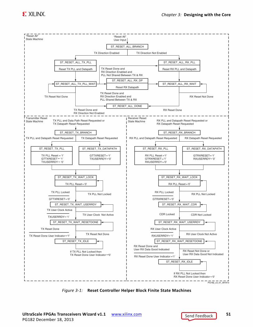
UltraScale FPGAs Transceivers Wizard v1.1 www.xilinx.com 51PG182 December 18, 2013
Chapter 3: Designing with the Core
X-Ref Target - Figure 3-1
Figure 3‐1: Reset Controller Helper Block Finite State Machines
Transmitter ResetState Machine
Receiver ResetState Machine
“Reset All”State Machine
ST_RESET_TX_BRANCH
TX PLL and Datapath Reset Requested TX Datapath Reset Requested
TX PLL Not Locked
ST_RESET_TX_WAIT_USERRDY
TX User Clock Active
TXUSERRDY ‘1’
TX PLL Locked
GTTXRESET ‘0’
TX User Clock Not Active
ST_RESET_TX_WAIT_RESETDONE
TX Reset Not Done
TX Reset Done
TX Reset Done User Indicator ‘1’
ST_RESET_TX_IDLE
If TX PLL Not Locked thenTX Reset Done User Indicator ‘0’
ST_RESET_TX_PLL
TX PLL Reset ‘1’GTTXRESET ‘1’TXUSERRDY ‘0’
ST_RESET_TX_DATAPATH
GTTXRESET ‘1’TXUSERRDY ‘0’
ST_RESET_TX_WAIT_LOCK
TX PLL Reset ‘0’
ST_RESET_RX_BRANCH
RX PLL and Datapath Reset Requested RX Datapath Reset Requested
RX PLL Not Locked
ST_RESET_RX_WAIT_CDR
CDR Locked
RX PLL Locked
GTRXRESET ‘0’
CDR Not Locked
ST_RESET_RX_WAIT_RESETDONE
RX Reset Not Done orUser RX Data Good Not Indicated
RX Reset Done andUser RX Data Good Indicated
RX Reset Done User Indicator ‘1’
ST_RESET_RX_IDLE
If RX PLL Not Locked thenRX Reset Done User Indicator ‘0’
ST_RESET_RX_PLL
RX PLL Reset ‘1’GTRXRESET ‘1’RXUSERRDY ‘0’
ST_RESET_RX_DATAPATH
GTRXRESET ‘1’RXUSERRDY ‘0’
ST_RESET_RX_WAIT_LOCK
RX PLL Reset ‘0’
ST_RESET_RX_WAIT_USERRDY
RX User Clock Not Active
RX User Clock Active
RXUSERRDY ‘1’
ST_RESET_ALL_BRANCH
ST_RESET_ALL_TX_PLL
Reset TX PLL and Datapath
ST_RESET_ALL_RX_PLL
Reset RX PLL and Datapath
TX Direction Enabled TX Direction Not Enabled
ST_RESET_ALL_TX_PLL_WAIT
TX Reset Not Done
TX Reset Done andRX Direction Enabled andPLL Not Shared Between TX & RX
TX Reset Done andRX Direction Enabled andPLL Shared Between TX & RX
ST_RESET_ALL_RX_DP
Reset RX DatapathST_RESET_ALL_RX_WAIT
ST_RESET_ALL_DONETX Reset Done andRX Direction Not Enabled
RX Reset Not Done
RX Reset Done
TX PLL and Data Path Reset Requested orTX Datapath Reset Requested
RX PLL and Datapath Reset Requested orRX Datapath Reset Requested
“Reset All”User Input
PG182_c3_01_091913
Send Feedback
UltraScale FPGAs Transceivers Wizard v1.1 www.xilinx.com 52PG182 December 18, 2013
Chapter 3: Designing with the Core
The transmitter reset state machine initiates a PLL reset followed by a transmitter datapath reset when the gtwiz_reset_tx_pll_and_datapath_in input is pulsed. All PLLs (either QPLL or CPLL type) instantiated by the core instance that are used to clock the transmitter datapath are reset in response to this input. After all these PLLs lock, the transmitter datapaths of all transceiver primitives are reset. If a PLL reset is not needed, a transmitter datapath-only reset is initiated when the gtwiz_reset_tx_datapath_in input is pulsed. Regardless of the reset entry point, the gtwiz_reset_tx_done_out indicator is asserted synchronous to transmitter master channel TXUSRCLK2 upon completion of the transmitter reset sequence for all transceiver primitives.
Likewise, the receiver reset state machine initiates a PLL reset followed by a receiver datapath reset when the gtwiz_reset_rx_pll_and_datapath_in input is pulsed. All PLLs (either QPLL or CPLL type) instantiated by the core instance that are used to clock the receiver datapath are reset in response to this input. When all these PLLs lock, the receiver datapaths of all transceiver primitives are reset. If a PLL reset is not needed, a receiver datapath-only reset is initiated when the gtwiz_reset_rx_datapath_in input is pulsed. Regardless of the reset entry point, the gtwiz_reset_rx_done_out indicator is asserted synchronous to receiver master channel RXUSRCLK2 upon completion of the receiver reset sequence for all transceiver primitives.
IMPORTANT: The independent transmitter and receiver reset state machines are simple and useful. However, because PLLs can be shared between transmitter and receiver datapaths, it is important to understand the potential system impacts when using the gtwiz_reset_tx_pll_and_datapath_in and gtwiz_reset_rx_pll_and_datapath_in inputs. For example, if both transmitter and receiver datapaths are clocked by QPLL0 resources, assertion of either of those two inputs would reset the shared QPLL0 of each transceiver Quad, causing potentially-unintended link loss in the other data direction. Use these inputs with caution, especially if PLL resources are shared with other core instances.
The reset all state machine can be used to avoid just such redundant PLL reset sequences. In addition, it resets the transmitter data direction before the receiver data direction (which can improve data integrity in loopback or some other circumstances) and is triggered by a simple one-input interface. The reset all state machine does not sequence transceiver primitive reset signals itself. Rather, it controls the transmitter and receiver reset state machines in the appropriate fashion for your core customization—effectively controlling some sequence of gtwiz_reset_tx_pll_and_datapath_in, gtwiz_reset_rx_pll_and_datapath_in, and gtwiz_reset_rx_datapath_in assertions. See Figure 3-1 to visualize the specif ic effects of the reset all state machine for your core customization.
Send Feedback
UltraScale FPGAs Transceivers Wizard v1.1 www.xilinx.com 53PG182 December 18, 2013
Chapter 3: Designing with the Core
Reset Sequencing and Other Services
The transmitter and receiver reset state machines implement the relevant reset sequences as specified in the UltraScale FPGAs GTH Transceivers User Guide (UG576) [Ref 1]. The reset controller helper block transceiver interface connects to the transceiver primitives. To implement proper TXUSERRDY and RXUSERRDY signaling, wiring exists between the reset controller helper block and both transmitter and receiver user clocking network helper blocks. Also, if the transmitter or receiver buffers are bypassed, wiring exists between the reset helper block and the relevant buffer bypass controller helper blocks to initiate the buffer bypass sequences upon completion of the reset sequences. This wiring exists regardless of the location of each helper block.
The receiver reset state machine provides a CDR stable indicator on the reset controller helper block user interface. In some configurations, the CDR stable indicator to the receiver user clocking network helper block to hold it in reset until the CDR is stable, thus indicating that RXOUTCLK is a stable clock source from which to derive RXUSRCLK and RXUSRCLK2.
Completion of the reset state machine sequence is gated by the gtwiz_reset_rx_data_good_in user interface input. The receiver PLL and receiver datapath reset sequences themselves are allowed to complete without regard to the value of this input, but the gtwiz_reset_rx_done_out user indicator does not assert during the receiver datapath reset sequence until gtwiz_reset_rx_data_good_in is asserted. Assert gtwiz_reset_rx_data_good_in only when data received from all transceivers has the expected data integrity characteristics.
When the transmitter reset state machine has completed, if one or more PLLs that clock transceiver primitive transmitter datapaths lose lock, the gtwiz_reset_tx_done_out user indicator is deasserted. A reset sequence does not automatically restart in this circumstance; user intervention is required.
Similarly, when the receiver reset state machine has completed, if one or more PLLs that clock transceiver primitive receiver datapaths lose lock, the gtwiz_reset_rx_done_out user indicator is deasserted. A reset sequence does not automatically restart in this circumstance; user intervention is required.
The helper block can be located either within the core or in the example design per user selection. Depending on its location and the location of other helper blocks, the relevant ports are enabled on the core interface so that the necessary signals can cross the core boundary.
If additional reset control or related ports are required for your application, or if you wish to observe individual transceiver primitive reset status signals, you can enable the relevant ports on the core instance using the optional ports interface during IP customization.
See Chapter 2, Product Specif ication, for a description of all reset controller block ports. See the UltraScale FPGAs GTH Transceivers User Guide (UG576) [Ref 1] for complete documentation on resetting and initializing the transceiver primitives.
Send Feedback
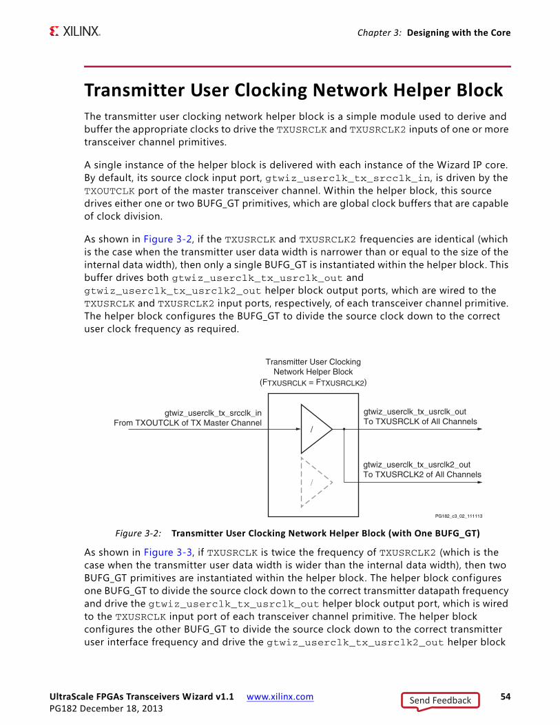
UltraScale FPGAs Transceivers Wizard v1.1 www.xilinx.com 54PG182 December 18, 2013
Chapter 3: Designing with the Core
Transmitter User Clocking Network Helper Block The transmitter user clocking network helper block is a simple module used to derive and buffer the appropriate clocks to drive the TXUSRCLK and TXUSRCLK2 inputs of one or more transceiver channel primitives.
A single instance of the helper block is delivered with each instance of the Wizard IP core. By default, its source clock input port, gtwiz_userclk_tx_srcclk_in, is driven by the TXOUTCLK port of the master transceiver channel. Within the helper block, this source drives either one or two BUFG_GT primitives, which are global clock buffers that are capable of clock division.
As shown in Figure 3-2, if the TXUSRCLK and TXUSRCLK2 frequencies are identical (which is the case when the transmitter user data width is narrower than or equal to the size of the internal data width), then only a single BUFG_GT is instantiated within the helper block. This buffer drives both gtwiz_userclk_tx_usrclk_out and gtwiz_userclk_tx_usrclk2_out helper block output ports, which are wired to the TXUSRCLK and TXUSRCLK2 input ports, respectively, of each transceiver channel primitive. The helper block configures the BUFG_GT to divide the source clock down to the correct user clock frequency as required.
As shown in Figure 3-3, if TXUSRCLK is twice the frequency of TXUSRCLK2 (which is the case when the transmitter user data width is wider than the internal data width), then two BUFG_GT primitives are instantiated within the helper block. The helper block configures one BUFG_GT to divide the source clock down to the correct transmitter datapath frequency and drive the gtwiz_userclk_tx_usrclk_out helper block output port, which is wired to the TXUSRCLK input port of each transceiver channel primitive. The helper block configures the other BUFG_GT to divide the source clock down to the correct transmitter user interface frequency and drive the gtwiz_userclk_tx_usrclk2_out helper block
X-Ref Target - Figure 3-2
Figure 3‐2: Transmitter User Clocking Network Helper Block (with One BUFG_GT)
PG182_c3_02_111113
gtwiz_userclk_tx_srcclk_inFrom TXOUTCLK of TX Master Channel
gtwiz_userclk_tx_usrclk_outTo TXUSRCLK of All Channels
gtwiz_userclk_tx_usrclk2_outTo TXUSRCLK2 of All Channels
Transmitter User ClockingNetwork Helper Block
(FTXUSRCLK = FTXUSRCLK2)
/
/
Send Feedback
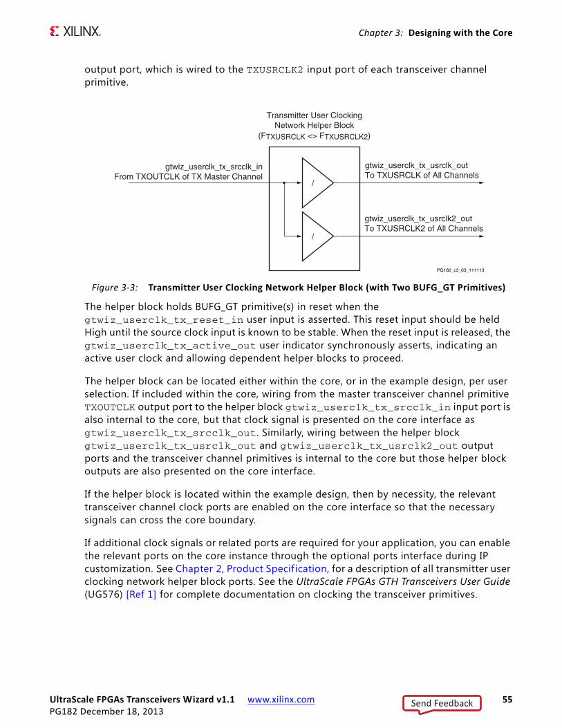
UltraScale FPGAs Transceivers Wizard v1.1 www.xilinx.com 55PG182 December 18, 2013
Chapter 3: Designing with the Core
output port, which is wired to the TXUSRCLK2 input port of each transceiver channel primitive.
The helper block holds BUFG_GT primitive(s) in reset when the gtwiz_userclk_tx_reset_in user input is asserted. This reset input should be held High until the source clock input is known to be stable. When the reset input is released, the gtwiz_userclk_tx_active_out user indicator synchronously asserts, indicating an active user clock and allowing dependent helper blocks to proceed.
The helper block can be located either within the core, or in the example design, per user selection. If included within the core, wiring from the master transceiver channel primitive TXOUTCLK output port to the helper block gtwiz_userclk_tx_srcclk_in input port is also internal to the core, but that clock signal is presented on the core interface as gtwiz_userclk_tx_srcclk_out. Similarly, wiring between the helper block gtwiz_userclk_tx_usrclk_out and gtwiz_userclk_tx_usrclk2_out output ports and the transceiver channel primitives is internal to the core but those helper block outputs are also presented on the core interface.
If the helper block is located within the example design, then by necessity, the relevant transceiver channel clock ports are enabled on the core interface so that the necessary signals can cross the core boundary.
If additional clock signals or related ports are required for your application, you can enable the relevant ports on the core instance through the optional ports interface during IP customization. See Chapter 2, Product Specification, for a description of all transmitter user clocking network helper block ports. See the UltraScale FPGAs GTH Transceivers User Guide (UG576) [Ref 1] for complete documentation on clocking the transceiver primitives.
X-Ref Target - Figure 3-3
Figure 3‐3: Transmitter User Clocking Network Helper Block (with Two BUFG_GT Primitives)
PG182_c3_03_111113
gtwiz_userclk_tx_srcclk_inFrom TXOUTCLK of TX Master Channel
gtwiz_userclk_tx_usrclk_outTo TXUSRCLK of All Channels
gtwiz_userclk_tx_usrclk2_outTo TXUSRCLK2 of All Channels
Transmitter User ClockingNetwork Helper Block
(FTXUSRCLK <> FTXUSRCLK2)
/
/
Send Feedback
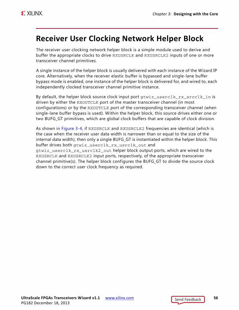
UltraScale FPGAs Transceivers Wizard v1.1 www.xilinx.com 56PG182 December 18, 2013
Chapter 3: Designing with the Core
Receiver User Clocking Network Helper Block The receiver user clocking network helper block is a simple module used to derive and buffer the appropriate clocks to drive RXUSRCLK and RXUSRCLK2 inputs of one or more transceiver channel primitives.
A single instance of the helper block is usually delivered with each instance of the Wizard IP core. Alternatively, when the receiver elastic buffer is bypassed and single-lane buffer bypass mode is enabled, one instance of the helper block is delivered for, and wired to, each independently clocked transceiver channel primitive instance.
By default, the helper block source clock input port gtwiz_userclk_rx_srcclk_in is driven by either the RXOUTCLK port of the master transceiver channel (in most configurations) or by the RXOUTCLK port of the corresponding transceiver channel (when single-lane buffer bypass is used). Within the helper block, this source drives either one or two BUFG_GT primitives, which are global clock buffers that are capable of clock division.
As shown in Figure 3-4, if RXUSRCLK and RXUSRCLK2 frequencies are identical (which is the case when the receiver user data width is narrower than or equal to the size of the internal data width), then only a single BUFG_GT is instantiated within the helper block. This buffer drives both gtwiz_userclk_rx_usrclk_out and gtwiz_userclk_rx_usrclk2_out helper block output ports, which are wired to the RXUSRCLK and RXUSRCLK2 input ports, respectively, of the appropriate transceiver channel primitive(s). The helper block configures the BUFG_GT to divide the source clock down to the correct user clock frequency as required.
Send Feedback
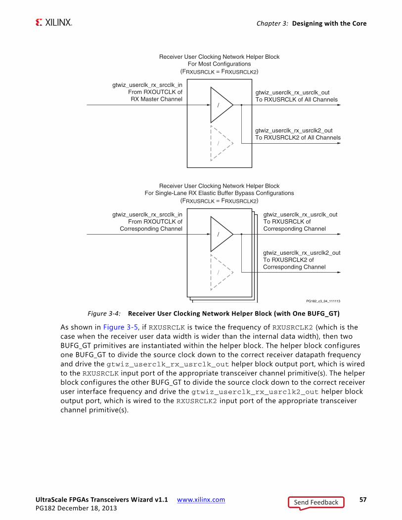
UltraScale FPGAs Transceivers Wizard v1.1 www.xilinx.com 57PG182 December 18, 2013
Chapter 3: Designing with the Core
As shown in Figure 3-5, if RXUSRCLK is twice the frequency of RXUSRCLK2 (which is the case when the receiver user data width is wider than the internal data width), then two BUFG_GT primitives are instantiated within the helper block. The helper block configures one BUFG_GT to divide the source clock down to the correct receiver datapath frequency and drive the gtwiz_userclk_rx_usrclk_out helper block output port, which is wired to the RXUSRCLK input port of the appropriate transceiver channel primitive(s). The helper block configures the other BUFG_GT to divide the source clock down to the correct receiver user interface frequency and drive the gtwiz_userclk_rx_usrclk2_out helper block output port, which is wired to the RXUSRCLK2 input port of the appropriate transceiver channel primitive(s).
X-Ref Target - Figure 3-4
Figure 3‐4: Receiver User Clocking Network Helper Block (with One BUFG_GT)
PG182_c3_04_111113
gtwiz_userclk_rx_srcclk_inFrom RXOUTCLK ofRX Master Channel
gtwiz_userclk_rx_usrclk_outTo RXUSRCLK of All Channels
gtwiz_userclk_rx_usrclk2_outTo RXUSRCLK2 of All Channels
Receiver User Clocking Network Helper BlockFor Most Configurations
(FRXUSRCLK = FRXUSRCLK2)
/
/
gtwiz_userclk_rx_srcclk_inFrom RXOUTCLK of
Corresponding Channel
gtwiz_userclk_rx_usrclk_outTo RXUSRCLK of Corresponding Channel
gtwiz_userclk_rx_usrclk2_outTo RXUSRCLK2 ofCorresponding Channel
Receiver User Clocking Network Helper BlockFor Single-Lane RX Elastic Buffer Bypass Configurations
(FRXUSRCLK = FRXUSRCLK2)
/
/
Send Feedback
UltraScale FPGAs Transceivers Wizard v1.1 www.xilinx.com 58PG182 December 18, 2013
Chapter 3: Designing with the Core
The helper block holds BUFG_GT primitive(s) in reset when the gtwiz_userclk_rx_reset_in user input is asserted. This reset input should be held High until the source clock input is known to be stable. When the reset input is released, the gtwiz_userclk_rx_active_out user indicator synchronously asserts, indicating an active user clock and allowing dependent helper blocks to proceed.
The helper block can be located either within the core or in the example design per user selection. If included within the core, wiring from the appropriate transceiver channel primitive RXOUTCLK output port(s) to the helper block gtwiz_userclk_rx_srcclk_in input port(s) is also internal to the core, but that clock signal is presented on the core interface as gtwiz_userclk_rx_srcclk_out.
Similarly, wiring between the helper block gtwiz_userclk_rx_usrclk_out and gtwiz_userclk_rx_usrclk2_out output ports and the transceiver channel primitives is internal to the core, but those helper block outputs are also presented on the core interface. If the helper block is located within the example design, then the relevant
X-Ref Target - Figure 3-5
Figure 3‐5: Receiver User Clocking Network Helper Block (with Two BUFG_GT Primitives)
PG182_c3_05_111113
gtwiz_userclk_rx_srcclk_inFrom RXOUTCLK ofRX Master Channel
gtwiz_userclk_rx_usrclk_outTo RXUSRCLK of All Channels
gtwiz_userclk_rx_usrclk2_outTo RXUSRCLK2 of All Channels
Receiver User Clocking Network Helper BlockFor Most Configurations
(FRXUSRCLK <> FRXUSRCLK2)
/
/
gtwiz_userclk_rx_srcclk_inFrom RXOUTCLK of
Corresponding Channel
gtwiz_userclk_rx_usrclk_outTo RXUSRCLK of Corresponding Channel
gtwiz_userclk_rx_usrclk2_outTo RXUSRCLK2 ofCorresponding Channel
Receiver User Clocking Network Helper BlockFor Single-lane RX Elastic Buffer Bypass Configurations
(FRXUSRCLK <> FRXUSRCLK2)
/
/
Send Feedback
UltraScale FPGAs Transceivers Wizard v1.1 www.xilinx.com 59PG182 December 18, 2013
Chapter 3: Designing with the Core
transceiver channel clock ports are enabled on the core interface so that the necessary signals can cross the core boundary.
If additional clock signals or related ports are required for your application, you can enable the relevant ports on the core instance through the optional ports interface during IP customization. See Chapter 2, Product Specif ication, for a description of all receiver user clocking network helper block ports. See the UltraScale FPGAs GTH Transceivers User Guide (UG576) [Ref 1] for complete documentation on clocking the transceiver primitives.
User Data Width Sizing Helper BlockThe user data width sizing helper block simplif ies the process of interfacing to the transmitter and receiver data ports of the transceiver channel primitives.
The TXDATA and RXDATA ports of each transceiver channel are 128 bits, but only those bits within the range of the configured transmitter and receiver user data widths are used; other bits are to be tied off or left unconnected, respectively. When multiple channels are enabled, it can be inconvenient to identify the active bits of the txdata_in and rxdata_out core port vectors. Furthermore, for user data widths of 20, 40, 80, or 160 bits, portions of TXCTRL0 and TXCTRL1 are interleaved with TXDATA, and portions of RXCTRL0 and RXCTRL1 are interleaved with RXDATA.
The helper block handles this transceiver-facing complexity while providing a simple user interface sized to the chosen user data width utilizing wiring only. The helper block is divided into two independent modules: a transmitter module and a receiver module. Both modules use generated HDL wire assignments. Because no combinatorial or sequential logic is used, there is no impact on the datapath.
Transmitter Module
The helper block transmitter module port gtwiz_userdata_tx_in is a vector sized to the chosen transmitter user data width, multiplied by the number of enabled transceiver channels. By core convention, its least signif icant bits correspond to the least significant bits of the transceiver channel in the lowest enabled XY grid position.
Figure 3-6 shows the helper block configuration for an example core configuration using a 32-bit transmitter user data width and four enabled transceiver channels. With the resulting packed 128-bit gtwiz_userdata_tx_in vector, the helper block drives the appropriate bits of each transceiver channel’s TXDATA port. For 20-, 40-, 80-, and 160-bit transmitter user data widths, it also drives the appropriate bits of each transceiver channel’s TXCTRL0 and TXCTRL1 ports, handling the required de-interleaving. In other configurations, the TXCTRL0 and TXCTRL1 ports are not driven by the helper block and are available for user access.
Send Feedback
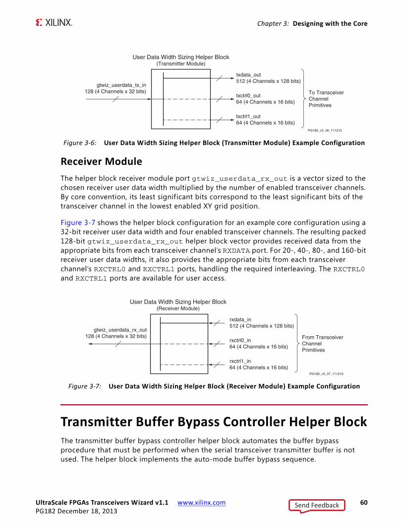
UltraScale FPGAs Transceivers Wizard v1.1 www.xilinx.com 60PG182 December 18, 2013
Chapter 3: Designing with the Core
Receiver Module
The helper block receiver module port gtwiz_userdata_rx_out is a vector sized to the chosen receiver user data width multiplied by the number of enabled transceiver channels. By core convention, its least significant bits correspond to the least signif icant bits of the transceiver channel in the lowest enabled XY grid position.
Figure 3-7 shows the helper block configuration for an example core configuration using a 32-bit receiver user data width and four enabled transceiver channels. The resulting packed 128-bit gtwiz_userdata_rx_out helper block vector provides received data from the appropriate bits from each transceiver channel’s RXDATA port. For 20-, 40-, 80-, and 160-bit receiver user data widths, it also provides the appropriate bits from each transceiver channel’s RXCTRL0 and RXCTRL1 ports, handling the required interleaving. The RXCTRL0 and RXCTRL1 ports are available for user access.
Transmitter Buffer Bypass Controller Helper BlockThe transmitter buffer bypass controller helper block automates the buffer bypass procedure that must be performed when the serial transceiver transmitter buffer is not used. The helper block implements the auto-mode buffer bypass sequence.
X-Ref Target - Figure 3-6
Figure 3‐6: User Data Width Sizing Helper Block (Transmitter Module) Example Configuration
X-Ref Target - Figure 3-7
Figure 3‐7: User Data Width Sizing Helper Block (Receiver Module) Example Configuration
gtwiz_userdata_tx_in128 (4 Channels x 32 bits)
PG182_c3_06_111213
txdata_out512 (4 Channels x 128 bits)
txctrl0_out64 (4 Channels x 16 bits)
txctrl1_out64 (4 Channels x 16 bits)
User Data Width Sizing Helper Block(Transmitter Module)
To TransceiverChannelPrimitives
gtwiz_userdata_rx_out128 (4 Channels x 32 bits)
PG182_c3_07_111213
rxdata_in512 (4 Channels x 128 bits)
rxctrl0_in64 (4 Channels x 16 bits)
rxctrl1_in64 (4 Channels x 16 bits)
User Data Width Sizing Helper Block(Receiver Module)
From TransceiverChannelPrimitives
Send Feedback
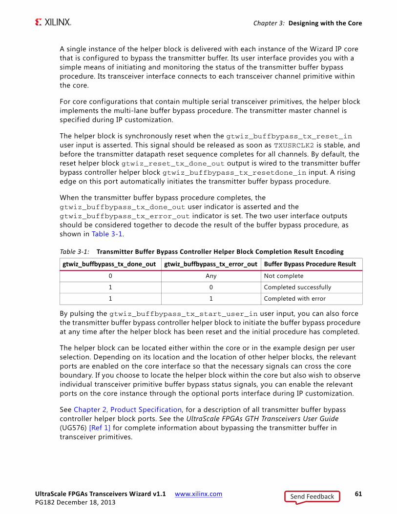
UltraScale FPGAs Transceivers Wizard v1.1 www.xilinx.com 61PG182 December 18, 2013
Chapter 3: Designing with the Core
A single instance of the helper block is delivered with each instance of the Wizard IP core that is configured to bypass the transmitter buffer. Its user interface provides you with a simple means of initiating and monitoring the status of the transmitter buffer bypass procedure. Its transceiver interface connects to each transceiver channel primitive within the core.
For core configurations that contain multiple serial transceiver primitives, the helper block implements the multi-lane buffer bypass procedure. The transmitter master channel is specified during IP customization.
The helper block is synchronously reset when the gtwiz_buffbypass_tx_reset_in user input is asserted. This signal should be released as soon as TXUSRCLK2 is stable, and before the transmitter datapath reset sequence completes for all channels. By default, the reset helper block gtwiz_reset_tx_done_out output is wired to the transmitter buffer bypass controller helper block gtwiz_buffbypass_tx_resetdone_in input. A rising edge on this port automatically initiates the transmitter buffer bypass procedure.
When the transmitter buffer bypass procedure completes, the gtwiz_buffbypass_tx_done_out user indicator is asserted and the gtwiz_buffbypass_tx_error_out indicator is set. The two user interface outputs should be considered together to decode the result of the buffer bypass procedure, as shown in Table 3-1.
By pulsing the gtwiz_buffbypass_tx_start_user_in user input, you can also force the transmitter buffer bypass controller helper block to initiate the buffer bypass procedure at any time after the helper block has been reset and the initial procedure has completed.
The helper block can be located either within the core or in the example design per user selection. Depending on its location and the location of other helper blocks, the relevant ports are enabled on the core interface so that the necessary signals can cross the core boundary. If you choose to locate the helper block within the core but also wish to observe individual transceiver primitive buffer bypass status signals, you can enable the relevant ports on the core instance through the optional ports interface during IP customization.
See Chapter 2, Product Specif ication, for a description of all transmitter buffer bypass controller helper block ports. See the UltraScale FPGAs GTH Transceivers User Guide (UG576) [Ref 1] for complete information about bypassing the transmitter buffer in transceiver primitives.
Table 3‐1: Transmitter Buffer Bypass Controller Helper Block Completion Result Encoding
gtwiz_buffbypass_tx_done_out gtwiz_buffbypass_tx_error_out Buffer Bypass Procedure Result
0 Any Not complete
1 0 Completed successfully
1 1 Completed with error
Send Feedback
UltraScale FPGAs Transceivers Wizard v1.1 www.xilinx.com 62PG182 December 18, 2013
Chapter 3: Designing with the Core
Receiver Buffer Bypass Controller Helper BlockThe receiver buffer bypass controller helper block automates the buffer bypass procedure, which must be performed when the serial transceiver receiver elastic buffer is not used. The helper block implements the auto-mode buffer bypass sequence. When the Wizard is configured to bypass the receiver elastic buffer, the following takes place:
• If multi-lane buffer bypass mode is enabled, one instance of the helper block is delivered and implements the multi-lane buffer bypass procedure. In this case, the user interface port width is not scaled, while the transceiver interface is scaled to the number of channel primitives in the core.
• If single-lane buffer bypass mode is enabled, an instance of the helper block is delivered for, and wired to each transceiver channel primitive instance. In this case, the user interface port width scales with the number of helper blocks, while the transceiver interface connects to its corresponding channel primitive only.
The helper block user interface provides you with a simple means of initiating and monitoring the status of the receiver buffer bypass procedure. Its transceiver interface connects to transceiver channel primitive(s) within the core.
The helper block is synchronously reset when the gtwiz_buffbypass_rx_reset_in user input is asserted. This signal should be released as soon as RXUSRCLK2 of the receiver master channel (for multi-lane buffer bypass configurations), or RXUSRCLK2 of the corresponding channel (for single-lane buffer bypass configurations) is stable, and before the receiver datapath reset sequence completes for all channels. By default, the reset helper block gtwiz_reset_rx_done_out output is wired to the receiver buffer bypass controller helper block gtwiz_buffbypass_rx_resetdone_in input. A rising edge on this port automatically initiates the receiver buffer bypass procedure.
When the receiver buffer bypass procedure completes, the gtwiz_buffbypass_rx_done_out user indicator is asserted and the gtwiz_buffbypass_rx_error_out indicator is set. The two user interface outputs should be considered together to decode the result of the buffer bypass procedure, as shown in Table 3-2.
You can force the receiver buffer bypass controller helper block to initiate the buffer bypass procedure at any time after the helper block has been reset and the initial procedure has completed by pulsing the gtwiz_buffbypass_rx_start_user_in user input.
Table 3‐2: Transmitter Buffer Bypass Controller Helper Block Completion Result Encoding
gtwiz_buffbypass_rx_done_out gtwiz_buffbypass_rx_error_out Buffer Bypass Procedure Result
0 Any Not complete
1 0 Completed successfully
1 1 Completed with error
Send Feedback
UltraScale FPGAs Transceivers Wizard v1.1 www.xilinx.com 63PG182 December 18, 2013
Chapter 3: Designing with the Core
The helper block can be located either within the core or in the example design per user selection. Depending on its location and the location of other helper blocks, the relevant ports are enabled on the core interface so that the necessary signals can cross the core boundary.
If you choose to locate the helper block within the core but also wish to observe individual transceiver primitive buffer bypass status signals, you can enable the relevant ports on the core instance through the optional ports interface during IP customization.
See Chapter 2, Product Specif ication, for a description of all receiver buffer bypass controller helper block ports. See the UltraScale FPGAs GTH Transceivers User Guide (UG576) [Ref 1] for complete documentation on bypassing the receiver elastic buffer in transceiver primitives.
Transceiver Common PrimitiveThe transceiver common primitive is required and instantiated for core configurations where QPLL0 or QPLL1 clocking resources are used. Although it is a transceiver primitive, its logical location can be specif ied during IP customization. Like a helper block, it can be located either within the core or in the example design.
By providing this flexibility, it is possible to share a single transceiver common between multiple Wizard IP core instances in these situations:
• You attempt to place the physical transceiver resources of those core instances into a single transceiver Quad
• The transceiver common configuration is identical or otherwise safe to share between the two core instances
Transceiver common sharing between core instances is an advanced use mode and should only be performed when restrictions and limitations are fully understood. See the UltraScale FPGAs GTH Transceivers User Guide (UG576) [Ref 1] for details on the use of the transceiver common primitive.
Figure 3-8 illustrates the case where one or more transceiver common primitives are enabled and located within the core instance, when user-specif ied. In this case, the QPLL#OUTCLK and QPLL#OUTREFCLK ports of the transceiver common primitives internally drive the QPLL#CLK and QPLL#REFCLK ports of the associated transceiver channel primitives, as required (where # is 0 or 1 for QPLL0 or QPLL1, respectively). However, those same signals are also provided as outputs on the core interface as qpll#outclk_out and qpll#outrefclk_out.
Send Feedback
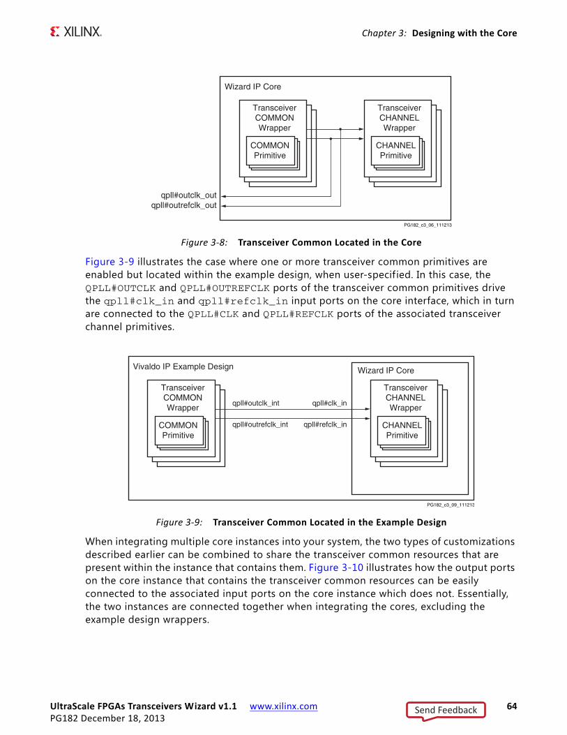
UltraScale FPGAs Transceivers Wizard v1.1 www.xilinx.com 64PG182 December 18, 2013
Chapter 3: Designing with the Core
Figure 3-9 illustrates the case where one or more transceiver common primitives are enabled but located within the example design, when user-specif ied. In this case, the QPLL#OUTCLK and QPLL#OUTREFCLK ports of the transceiver common primitives drive the qpll#clk_in and qpll#refclk_in input ports on the core interface, which in turn are connected to the QPLL#CLK and QPLL#REFCLK ports of the associated transceiver channel primitives.
When integrating multiple core instances into your system, the two types of customizations described earlier can be combined to share the transceiver common resources that are present within the instance that contains them. Figure 3-10 illustrates how the output ports on the core instance that contains the transceiver common resources can be easily connected to the associated input ports on the core instance which does not. Essentially, the two instances are connected together when integrating the cores, excluding the example design wrappers.
X-Ref Target - Figure 3-8
Figure 3‐8: Transceiver Common Located in the Core
X-Ref Target - Figure 3-9
Figure 3‐9: Transceiver Common Located in the Example Design
Wizard IP Core
TransceiverCHANNELWrapper
CHANNELPrimitive
TransceiverCOMMONWrapper
COMMONPrimitive
qpll#outclk_outqpll#outrefclk_out
PG182_c3_06_111213
Vivaldo IP Example Design Wizard IP Core
TransceiverCHANNELWrapper
CHANNELPrimitive
TransceiverCOMMONWrapper
qpll#outclk_int
qpll#outrefclk_int
qpll#clk_in
qpll#refclk_inCOMMONPrimitive
PG182_c3_09_111213
Send Feedback
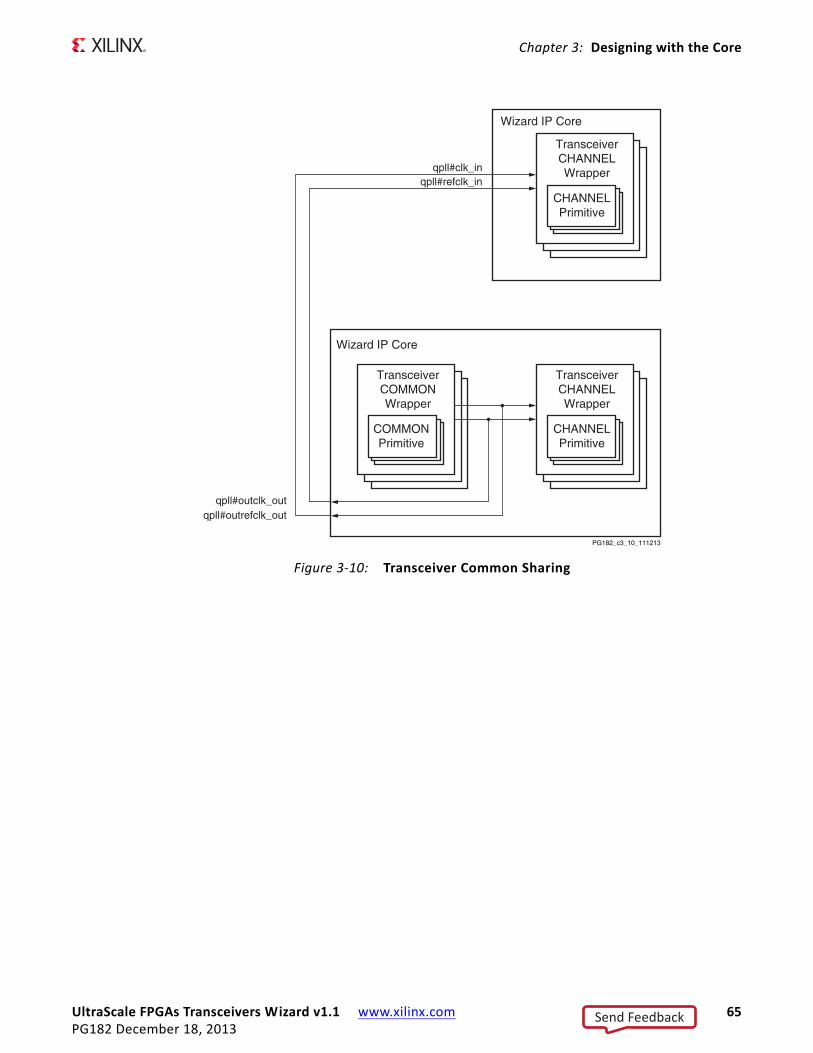
UltraScale FPGAs Transceivers Wizard v1.1 www.xilinx.com 65PG182 December 18, 2013
Chapter 3: Designing with the Core
X-Ref Target - Figure 3-10
Figure 3‐10: Transceiver Common Sharing
Wizard IP Core
Wizard IP Core
TransceiverCHANNELWrapper
CHANNELPrimitive
TransceiverCHANNELWrapper
CHANNELPrimitive
TransceiverCOMMONWrapper
COMMONPrimitive
qpll#outclk_outqpll#outrefclk_out
qpll#clk_inqpll#refclk_in
PG182_c3_10_111213
Send Feedback
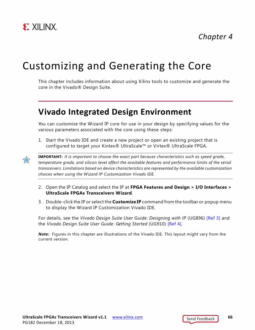
UltraScale FPGAs Transceivers Wizard v1.1 www.xilinx.com 66PG182 December 18, 2013
Chapter 4
Customizing and Generating the CoreThis chapter includes information about using Xilinx tools to customize and generate the core in the Vivado® Design Suite.
Vivado Integrated Design EnvironmentYou can customize the Wizard IP core for use in your design by specifying values for the various parameters associated with the core using these steps:
1. Start the Vivado IDE and create a new project or open an existing project that is configured to target your Kintex® UltraScale™ or Virtex® UltraScale FPGA.
IMPORTANT: It is important to choose the exact part because characteristics such as speed grade, temperature grade, and silicon level affect the available features and performance limits of the serial transceivers. Limitations based on device characteristics are represented by the available customization choices when using the Wizard IP Customization Vivado IDE.
2. Open the IP Catalog and select the IP at FPGA Features and Design > I/O Interfaces > UltraScale FPGAs Transceivers Wizard.
3. Double-click the IP or select the Customize IP command from the toolbar or popup menu to display the Wizard IP Customization Vivado IDE.
For details, see the Vivado Design Suite User Guide: Designing with IP (UG896) [Ref 3] and the Vivado Design Suite User Guide: Getting Started (UG910) [Ref 4].
Note: Figures in this chapter are illustrations of the Vivado IDE. This layout might vary from the current version.
Send Feedback
UltraScale FPGAs Transceivers Wizard v1.1 www.xilinx.com 67PG182 December 18, 2013
Chapter 4: Customizing and Generating the Core
Customization Vivado IDE OrganizationThe Wizard IP Customization Vivado IDE is organized in four tabs:
• Basic. Provides customization options for fundamental transceiver features, including transceiver type, and transmitter and receiver settings. Also provides the ability to select a transceiver configuration preset.
• Physical Resources. Provides table and graphical interfaces to select specif ic transceiver channel sites to enable, as well as reference clock routing options.
• Optional Features. Provides extensive configuration options for optional or advanced features, if appropriate for your application.
• Structural Options. Provides location choices for each available helper block, and the optional port enablement interface.
Review each of the available options and modify them as desired so that the resulting core instance meets your system requirements. For a full understanding of transceiver primitive features and available use modes, see the UltraScale FPGAs GTH Transceivers User Guide (UG576) [Ref 1].
Component Name and Symbol
The name of the generated IP is set in the Component Name field. The default name is gtwizard_ultrascale_0. This must be set to a name that is unique within your project.
The IP symbol is shown on the left-hand side of the IP Customization Vivado IDE, and displays only enabled ports by default. It organizes input ports on the left-hand side of the symbol and output ports on the right-hand side. The IP symbol is updated as you make customization choices and use the optional ports enablement interface. See Chapter 2, Product Specification for a detailed description of ports and their use.
Basic Tab
IP customization options in the Basic tab (Figure 4-1) are described in the following subsections. Selections apply to each enabled transceiver channel in the core instance. See the UltraScale FPGAs GTH Transceivers User Guide (UG576) [Ref 1] for full details on available choices for each customization option.
Send Feedback
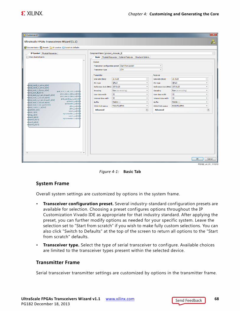
UltraScale FPGAs Transceivers Wizard v1.1 www.xilinx.com 68PG182 December 18, 2013
Chapter 4: Customizing and Generating the Core
System Frame
Overall system settings are customized by options in the system frame.
• Transceiver configuration preset. Several industry-standard configuration presets are available for selection. Choosing a preset configures options throughout the IP Customization Vivado IDE as appropriate for that industry standard. After applying the preset, you can further modify options as needed for your specific system. Leave the selection set to “Start from scratch” if you wish to make fully custom selections. You can also click "Switch to Defaults" at the top of the screen to return all options to the "Start from scratch" defaults.
• Transceiver type. Select the type of serial transceiver to configure. Available choices are limited to the transceiver types present within the selected device.
Transmitter Frame
Serial transceiver transmitter settings are customized by options in the transmitter frame.
X-Ref Target - Figure 4-1
Figure 4‐1: Basic Tab
PG182_c4_01_111213
Send Feedback
UltraScale FPGAs Transceivers Wizard v1.1 www.xilinx.com 69PG182 December 18, 2013
Chapter 4: Customizing and Generating the Core
• Line rate (Gb/s). Enter the transmitter line rate in gigabits per second. The available range depends on transceiver type and can be limited by the selected device.
• PLL type. Select the desired PLL type used to clock the transmitter of each enabled serial transceiver channel. Possible options are QPLL0, QPLL1, and CPLL, but available choices can be limited by the selected device and transmitter line rate. When QPLL0 or QPLL1 is chosen, one or more transceiver common primitives is instantiated. If the transmitter and receiver line rates differ, different PLL types might be required for each data direction.
• Reference clock (MHz). Select the desired frequency, from among all compatible frequencies, for the reference clock that will be provided to the selected PLL type to achieve the selected transmitter line rate.
• Encoding. Select the type of encoding or data format handling you want the transceiver to apply when data is transmitted. The options and their characteristics are:
° Raw (no encoding). Data is transmitted as provided.
° 8B/10B. Data is encoded in 8B/10B format before being transmitted.
° Sync. gearbox for 64B/66B. Data is transmitted using the TX Synchronous Gearbox in normal mode for 64B/66B applications.
° Sync. gearbox for 64B/66B (CAUI mode). Data is transmitted using the TX Synchronous Gearbox in CAUI (dual data stream) mode for 64B/66B applications.
° Async. gearbox for 64B/66B. Data is transmitted using the TX Asynchronous Gearbox in normal mode for 64B/66B applications.
° Async. gearbox for 64B/66B (CAUI mode). Data is transmitted using the TX Asynchronous Gearbox in CAUI (dual data stream) mode for 64B/66B applications.
° Sync. gearbox for 64B/67B. Data is transmitted using the TX Synchronous Gearbox in normal mode for 64B/67B applications.
° Sync. gearbox for 64B/67B (CAUI mode). Data is transmitted using the TX Synchronous Gearbox in CAUI (dual data stream) mode for 64B/67B applications.
• User data width. Also known as external data width. Select the desired bit width for the transmitter user data interface of each serial transceiver channel. Possible options are 16, 20, 32, 40, 64, 80, 128, and 160 but available choices can be limited by selected device, transceiver type, line rate, and encoding. This selection sets the active portion of the transmitter data vector, which is presented at full size on the core interface unless the user data width sizing helper block is located within the core. The active portion of the transmitter data vector is least significant bit-aligned. Inactive bits should be tied Low.
• Internal data width. Select the desired bit width for the internal transmitter datapath of each serial transceiver channel. Possible options are 16, 20, 32, 40, 64, and 80, but available choices are limited by selected device, transceiver type, line rate, encoding, and user data width.
Send Feedback
UltraScale FPGAs Transceivers Wizard v1.1 www.xilinx.com 70PG182 December 18, 2013
Chapter 4: Customizing and Generating the Core
• Buffer. Choose whether to enable or bypass the transmitter buffer. The ability to bypass the buffer might be limited by the selected encoding. When the buffer is bypassed, the transmitter buffer bypass controller helper block is provided.
• TXOUTCLK source. Select the internal clock source for the TXOUTCLK port of each serial transceiver primitive. Possible options are TXPLLREFCLK_DIV1, TXPLLREFCLK_DIV2, TXOUTCLKPCS, TXOUTCLKPMA, and TXPROGDIVCLK, but available choices can be limited by selected device, line rate, reference clock frequency, encoding, internal data width, and buffer usage. The transmitter user clocking network helper block is driven by the TXOUTCLK port, and thus by this clock source, of the master transceiver channel.
Transmitter Frame (Advanced Section)
Advanced serial transceiver transmitter settings are customized by options in the collapsible portion of the transmitter frame. Click the title to expand the section.
Differential swing and emphasis mode. Select the transmitter driver mode. Selection determines the set of ports that control the transmitter driver swing and cursors.
Receiver Frame
Serial transceiver receiver settings are customized by options in the receiver frame.
• Line rate (Gb/s). Enter the receiver line rate in gigabits per second. The available range depends on transceiver type and can be limited by the selected device.
• PLL type. Select the desired PLL type used to clock the receiver of each enabled serial transceiver channel. Possible options are QPLL0, QPLL1, and CPLL, but available choices can be limited by the selected device and receiver line rate. When QPLL0 or QPLL1 is chosen, one or more transceiver common primitives will be instantiated. If the receiver and transmitter line rates differ, different PLL types might be required for each data direction.
• Reference clock (MHz). Select the desired frequency from among all compatible frequencies for the reference clock that will be provided to the selected PLL type to achieve the selected receiver line rate.
• Decoding. Select the type of decoding or data format handling you want the transceiver to apply when data is received. The options and their characteristics are:
° Raw (no decoding). Data is provided as received.
° 8B/10B. Received data is decoded from 8B/10B format.
° Sync. gearbox for 64B/66B. Data is received using the RX Synchronous Gearbox in normal mode for 64B/66B applications.
° Sync. gearbox for 64B/66B (CAUI mode). Data is received using the RX Synchronous Gearbox in CAUI (dual data stream) mode for 64B/66B applications.
Send Feedback
UltraScale FPGAs Transceivers Wizard v1.1 www.xilinx.com 71PG182 December 18, 2013
Chapter 4: Customizing and Generating the Core
° Async. gearbox for 64B/66B. Data is received using the RX Asynchronous Gearbox in normal mode for 64B/66B applications.
° Async. gearbox for 64B/66B (CAUI mode). Data is received using the RX Asynchronous Gearbox in CAUI (dual data stream) mode for 64B/66B applications.
° Sync. gearbox for 64B/67B. Data is received using the RX Synchronous Gearbox in normal mode for 64B/67B applications.
° Sync. gearbox for 64B/67B gearbox (CAUI mode). Data is received using the RX Synchronous Gearbox in CAUI (dual data stream) mode for 64B/67B applications.
• User data width. Also known as external data width. Select the desired bit width for the receiver user data interface of each serial transceiver channel. Possible options are 16, 20, 32, 40, 64, 80, 128, and 160 but available choices can be limited by selected device, transceiver type, line rate, and decoding. This selection sets the active portion of the receiver data vector, which is presented at full size on the core interface unless the user data width sizing helper block is located within the core. The active portion of the receiver data vector is least signif icant bit-aligned. Inactive bits should be ignored.
• Internal data width. Select the desired bit width for the internal receiver datapath of each serial transceiver channel. Possible options are 16, 20, 32, 40, 64, and 80, but available choices are limited by selected device, transceiver type, line rate, decoding, and user data width.
• Buffer. Choose whether to enable or bypass the receiver elastic buffer. The ability to bypass the buffer can be limited by the selected decoding. When the buffer is bypassed, the receiver buffer bypass controller helper block is provided.
• RXOUTCLK source. Select the internal clock source for the RXOUTCLK port of each serial transceiver primitive. Possible options are RXPLLREFCLK_DIV1, RXPLLREFCLK_DIV2, RXOUTCLKPCS, RXOUTCLKPMA, and RXPROGDIVCLK, but available choices can be limited by selected device, line rate, reference clock frequency, decoding, internal data width, and buffer usage. The receiver user clocking network helper block is driven by the RXOUTCLK port, and thus by this clock source, of either the master transceiver channel or of each transceiver channel (depending on buffer usage options).
Receiver Frame (Advanced Section)
Advanced serial transceiver receiver settings are customized by options in the collapsible portion of the receiver frame. Click the title to expand the section.
• Equalization mode. Select between decision feedback equalization (DFE) mode and low-power mode (LPM) for the receiver equalization. When the Auto option is selected, the mode is set automatically based on the channel insertion loss.
• Termination. Select the receiver termination voltage. Your choice of termination should depend on the protocol and its link coupling.
Send Feedback
UltraScale FPGAs Transceivers Wizard v1.1 www.xilinx.com 72PG182 December 18, 2013
Chapter 4: Customizing and Generating the Core
• Programmable termination voltage (mV). When termination is set to programmable, select the termination voltage in mV.
• Link coupling. Options are AC and DC. Select AC if external AC coupling is enabled in the application, and DC otherwise.
• PPM offset between receiver and transmitter. Specify the offset between received data and transmitter data in PPM. For example, if your protocol specif ies ±100 ppm, you would enter 200 in this f ield. This offset affects the receiver CDR settings.
• Spread spectrum clocking. Specify the spread spectrum clocking (SSC) modulation in PPM. SSC affects the receiver CDR settings.
• Insertion loss at Nyquist (dB). Specify the insertion loss of the channel between the transmitter and receiver at the Nyquist frequency in dB.
• Jitter tolerance mask: Mask corner frequency (MHz). Specify the corner frequency (or knee frequency) of the jitter tolerance mask required by the application. This value affects the receiver CDR settings.
• Jitter tolerance mask: Mask low frequency slope (dB/decade). Specify the low-frequency slope of the jitter tolerance mask required by the application. This value affects the receiver CDR settings.
Physical Resources Tab
IP customization options in the Physical Resources tab are described in the following subsections. When customizing options on this tab, it is important to understand that choices you make affect generated HDL and constraints. Select the options that are appropriate for your project and system. See the UltraScale FPGAs GTH Transceivers User Guide (UG576) [Ref 1] for details on the transceiver Quad architecture and reference clocking options. The layout of the Physical Resources tab is shown in Figure 4‐2.
Send Feedback
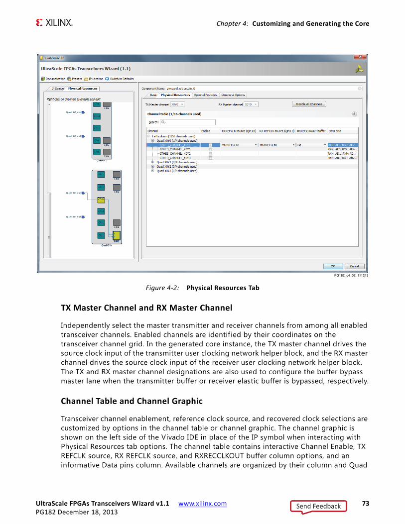
UltraScale FPGAs Transceivers Wizard v1.1 www.xilinx.com 73PG182 December 18, 2013
Chapter 4: Customizing and Generating the Core
TX Master Channel and RX Master Channel
Independently select the master transmitter and receiver channels from among all enabled transceiver channels. Enabled channels are identif ied by their coordinates on the transceiver channel grid. In the generated core instance, the TX master channel drives the source clock input of the transmitter user clocking network helper block, and the RX master channel drives the source clock input of the receiver user clocking network helper block. The TX and RX master channel designations are also used to configure the buffer bypass master lane when the transmitter buffer or receiver elastic buffer is bypassed, respectively.
Channel Table and Channel Graphic
Transceiver channel enablement, reference clock source, and recovered clock selections are customized by options in the channel table or channel graphic. The channel graphic is shown on the left side of the Vivado IDE in place of the IP symbol when interacting with Physical Resources tab options. The channel table contains interactive Channel Enable, TX REFCLK source, RX REFCLK source, and RXRECCLKOUT buffer column options, and an informative Data pins column. Available channels are organized by their column and Quad
X-Ref Target - Figure 4-2
Figure 4‐2: Physical Resources Tab
PG182_c4_02_111213
Send Feedback
UltraScale FPGAs Transceivers Wizard v1.1 www.xilinx.com 74PG182 December 18, 2013
Chapter 4: Customizing and Generating the Core
locations. The interactive channel graphic provides the same customization options and aids in visualizing transceiver primitive and reference clocking topology.
• Enabling a channel. To enable a particular transceiver channel for use, either click the corresponding checkbox in the channel table or right-click the channel in the graphic and select Enable. Enabling a channel causes that physical transceiver site to be instantiated, connected, and appropriately constrained in the generated core instance. Transceiver channels are organized by column and Quad, and are named according to their coordinates on the transceiver channel grid. Channels can also be identif ied by their serial data pins as shown in the Data pins column.
• Choosing a transmitter reference clock source. A valid transmitter reference clock source must be chosen for each enabled channel. You can choose a source from the TX REFCLK column of the channel table or by right-clicking the channel in the graphic. The transmitter PLL type selected during Basic tab customization is shown for reference. Choosing a reference clock source for a channel causes that buffered input to be routed to the channel, and for appropriate constraints to be generated. Each unique reference clock source selected requires a differential clock input to the device.
• Choosing a receiver reference clock source. A valid receiver reference clock source must be chosen for each enabled channel. You can choose a source from the RX REFCLK column of the channel table or by right-clicking the channel in the graphic. The receiver PLL type selected during Basic tab customization is shown for reference. Choosing a reference clock source for a channel causes that buffered input to be routed to the channel, and for appropriate constraints to be generated. Each unique reference clock source selected requires a differential clock input to the device.
Note: The Wizard always connects the buffered reference clock signal to the “GTREFCLK0” position of the appropriate PLL clock multiplexer(s) even if MGTREFCLK1 or a reference clock requiring north or south routing is selected. This is a supported simplif ication use mode, and the Vivado design tools handle the required routing complexity.
• Choosing a recovered clock source and buffer. The recovered clock of a transceiver channel can be buffered and driven out of the device. For an enabled transceiver channel, you can choose an available output buffer from the RXRECCLKOUT buffer column of the channel table, or by right-clicking the channel in the graphic. This feature requires using one of the available differential clock buffers within that transceiver’s Quad as an output, preventing that same resource from being used as a reference clock input buffer. Choosing a recovered clock source and buffer causes the channel’s recovered clock output to be routed to an instantiated output buffer primitive and the appropriate constraints to be generated.
Send Feedback
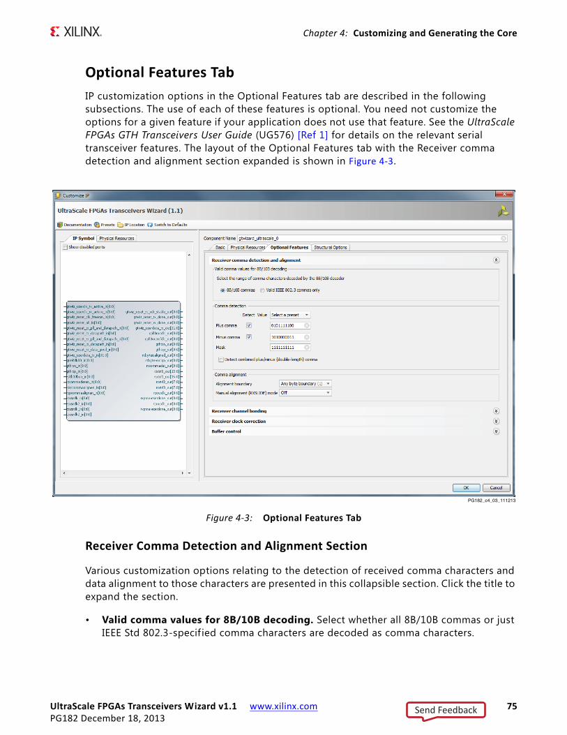
UltraScale FPGAs Transceivers Wizard v1.1 www.xilinx.com 75PG182 December 18, 2013
Chapter 4: Customizing and Generating the Core
Optional Features Tab
IP customization options in the Optional Features tab are described in the following subsections. The use of each of these features is optional. You need not customize the options for a given feature if your application does not use that feature. See the UltraScale FPGAs GTH Transceivers User Guide (UG576) [Ref 1] for details on the relevant serial transceiver features. The layout of the Optional Features tab with the Receiver comma detection and alignment section expanded is shown in Figure 4‐3.
Receiver Comma Detection and Alignment Section
Various customization options relating to the detection of received comma characters and data alignment to those characters are presented in this collapsible section. Click the title to expand the section.
• Valid comma values for 8B/10B decoding. Select whether all 8B/10B commas or just IEEE Std 802.3-specif ied comma characters are decoded as comma characters.
X-Ref Target - Figure 4-3
Figure 4‐3: Optional Features Tab
PG182_c4_03_111213
Send Feedback
UltraScale FPGAs Transceivers Wizard v1.1 www.xilinx.com 76PG182 December 18, 2013
Chapter 4: Customizing and Generating the Core
• Plus comma. Mark the checkbox under “Detect” to enable detection of the provided bit pattern as a plus comma. You can enter a pattern directly in the text box under “Value” or choose an option in the comma preset box to specify the standard plus comma pattern.
• Minus comma. Mark the checkbox under “Detect” to enable detection of the provided bit pattern as a minus comma. You can enter a pattern directly in the text box under “Value” or choose an option in the comma preset box to specify the standard minus comma pattern.
• Mask. Enter a comma mask bit pattern. Any bit set to “0” makes the comma detection block treat corresponding plus and minus comma values as a “don’t care”.
• Detect combined plus/minus (double length) comma. Mark the checkbox to enable the transceiver to search for the two commas in a row.
• Alignment boundary. Select which data byte boundaries are allowed for comma alignment. Possible options are any byte boundary, two byte boundaries, four byte boundaries, and eight byte boundaries, but available selections can be limited by receiver internal data width.
• Manual alignment (RXSLIDE) mode. If RXSLIDE will be used to implement manual alignment, select which mode to enable. Possible options are Off (to disable manual alignment), PCS, PMA, and Automated PMA, but available selections can be limited by receiver elastic buffer usage.
Receiver Channel Bonding Section
Various customization options relating to receiver channel bonding are presented in this collapsible section. Click the title to expand the section.
• Enable and select number of sequences to use. Select whether to enable receiver channel bonding, and if enabled, how many channel bonding sequences to use. Possible options are No channel bonding, 1, or 2 sequences, but available selections can be limited by the number of enabled channels, receiver data decoding, and receiver elastic buffer usage.
• Length of each sequence. When channel bonding is used, select the length of each channel bonding sequence. Options are 1, 2, and 4 patterns.
• Sequence maximum skew. When channel bonding is used, select a channel bonding maximum skew value that is less than half the minimum distance between instances of the channel bonding sequence. Options are 1, 2, 3, 4, 5, 6, 7, 8, 9, 10, 11, 12, 13, and 14 characters.
• Maximum channel bonding level to be used. When channel bonding is used, select the maximum channel bonding level that will be used in the channel bonding topology of the system. Options are 1, 2, 3, 4, 5, 6, and 7 levels.
Send Feedback
UltraScale FPGAs Transceivers Wizard v1.1 www.xilinx.com 77PG182 December 18, 2013
Chapter 4: Customizing and Generating the Core
• Don't care. For each pattern of each enabled channel bonding sequence, mark the checkbox to indicate that it should be treated as a “don’t care” and always considered as a match within a channel bonding sequence.
• Value. For each pattern of each enabled channel bonding sequence, specify its bit value.
• K character. For each pattern of each enabled channel bonding sequence, mark the checkbox to indicate that it is a K character.
• Inverted disparity. For each pattern of each enabled channel bonding sequence, mark the checkbox to indicate that it uses inverted disparity to signify control of a character by deliberate error.
Receiver Clock Correction Section
Various customization options relating to receiver clock correction are presented in this collapsible section. Click the title to expand the section.
• Enable and select number of sequences to use. Select whether to enable receiver clock correction, and if enabled, how many clock correction sequences to use. Possible options are No clock correction, 1, or 2 sequences, but available selections can be limited by receiver data decoding and receiver elastic buffer usage.
• Length of each sequence. When clock correction is used, select the length of each clock correction sequence. Options are 1, 2, and 4 patterns.
• Don’t care. For each pattern of each enabled clock correction sequence, mark the checkbox to indicate that it should be treated as a “don’t care” and always considered as a match within a clock correction sequence.
• Value. For each pattern of each enabled clock correction sequence, specify its bit value.
• K character. For each pattern of each enabled clock correction sequence, mark the checkbox to indicate that it is a K character.
• Inverted disparity. For each pattern of each enabled clock correction sequence, mark the checkbox to indicate that it uses inverted disparity to signify a control character by deliberate error.
• Periodicity of the sequence (in bytes). Specify the separation between clock correction sequences, in bytes.
• Keep idle. Specify whether at least one clock correction sequence is kept in the data stream for every continuous stream of clock correction sequences received. Options are Enable or Disable.
• Precedence. Specify whether clock correction takes precedence over channel bonding when both operations are triggered at the same time. Options are Enable or Disable.
Send Feedback
UltraScale FPGAs Transceivers Wizard v1.1 www.xilinx.com 78PG182 December 18, 2013
Chapter 4: Customizing and Generating the Core
• Minimum repetition. Specify the number of RXUSRCLK cycles following a clock correction during which the elastic buffer is not permitted to execute another clock correction. Legal options are 0 (for no limit), or 1 to 31 cycles.
Buffer Control Section
Various customization options relating to transmitter and receiver elastic buffer control and behaviors are presented in this collapsible section. Click the title to expand the section.
• Receiver elastic buffer bypass mode. When the receiver elastic buffer is bypassed and two or more transceiver channels are enabled, specify whether multi-lane buffer bypass mode or single-lane buffer bypass mode is used. When multi-lane mode is selected, the designated receiver master channel acts as the buffer bypass master lane and clock source for the one receiver user clocking network helper block instance that provides user clocks to the master and all slave lanes. When single-lane mode is selected, each transceiver channel receiver elastic buffer is bypassed individually, resulting in an instance of the receiver buffer bypass controller helper block and an instance of the receiver user clocking network helper block for each transceiver channel. The default is multi-lane mode.
• Reset receiver elastic buffer on channel bonding change. Specify whether the receiver elastic buffer is reset on change to RXCHANBONDMASTER, RXCHANBONDSLAVE, or RXCHANBONDLEVEL. When the receiver elastic buffer is used, options are Enable or Disable.
• Reset receiver elastic buffer on comma alignment. Specify whether the receiver elastic buffer is reset on comma alignment. When the receiver elastic buffer is used, options are Enable or Disable.
• Reset receiver elastic buffer on rate change. Specify whether the receiver elastic buffer is reset on rate change. When the receiver elastic buffer is used, options are Enable or Disable.
• Reset transmitter buffer on rate change. Specify whether the transmitter buffer is reset on rate change. When the transmitter buffer is used, options are Enable or Disable.
Structural Options Tab
IP customization options in the Structural Options tab are described in the following subsections. The layout of the Structural Options tab is shown in Figure 4‐4.
Send Feedback
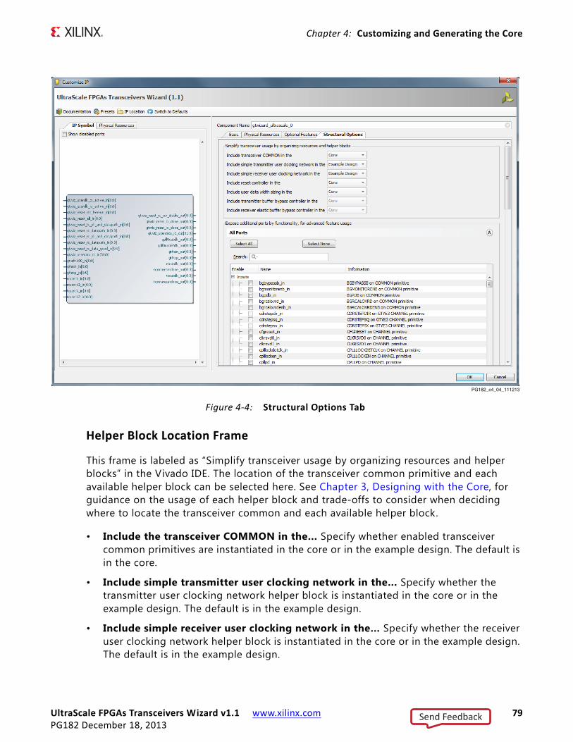
UltraScale FPGAs Transceivers Wizard v1.1 www.xilinx.com 79PG182 December 18, 2013
Chapter 4: Customizing and Generating the Core
Helper Block Location Frame
This frame is labeled as “Simplify transceiver usage by organizing resources and helper blocks” in the Vivado IDE. The location of the transceiver common primitive and each available helper block can be selected here. See Chapter 3, Designing with the Core, for guidance on the usage of each helper block and trade-offs to consider when deciding where to locate the transceiver common and each available helper block.
• Include the transceiver COMMON in the… Specify whether enabled transceiver common primitives are instantiated in the core or in the example design. The default is in the core.
• Include simple transmitter user clocking network in the… Specify whether the transmitter user clocking network helper block is instantiated in the core or in the example design. The default is in the example design.
• Include simple receiver user clocking network in the… Specify whether the receiver user clocking network helper block is instantiated in the core or in the example design. The default is in the example design.
X-Ref Target - Figure 4-4
Figure 4‐4: Structural Options Tab
PG182_c4_04_111213
Send Feedback
UltraScale FPGAs Transceivers Wizard v1.1 www.xilinx.com 80PG182 December 18, 2013
Chapter 4: Customizing and Generating the Core
• Include reset controller in the… Specify whether the reset controller helper block is instantiated in the core or in the example design. The default is in the core.
Note: If the example design is chosen as the location for the transceiver common, the reset controller must also be located in the example design.
• Include user width data sizing in the… Specify whether the user data width sizing helper block is instantiated in the core or in the example design.
• Include transmitter buffer bypass controller in the… If the transmitter buffer is bypassed, specify whether the transmitter buffer bypass controller helper block is instantiated in the core or in the example design. The default is in the core.
• Include receiver elastic buffer bypass controller in the… If the receiver elastic buffer is bypassed, specify whether the receiver buffer bypass controller helper block is instantiated in the core or in the example design. The default is in the core.
Optional Port Enablement Interface
This frame is labeled as “Expose additional ports by Functionality, for advanced feature usage” in the Vivado IDE. The optional port enablement interface allows additional transceiver channel and transceiver common primitive ports to be exposed on the core interface. See the UltraScale FPGAs GTH Transceivers User Guide (UG576) [Ref 1] for details on each available transceiver primitive port.
• All Ports. All Wizard ports are presented for optional enablement in this collapsible section. Click the title to expand the section and display the All Ports table. Ordering is alphabetical by port name, and organized according to port direction. The Name column of the table shows the Wizard IP core interface name for each port, while the Information column indicates the transceiver primitive type and mapping of that port (for non-helper block ports). Mark the checkbox for a given port in the Enable column to expose that port on the core interface. The IP symbol is updated to reflect the enabled ports. The search field can be used to search text within the All Ports collapsible section. Port enablement restrictions of the All Ports table are as follows:
° Helper block port enablement cannot be directly controlled and is a function of helper block availability and location only.
° Transceiver primitive input ports that are driven within the core instance, usually as a result of locating a helper block within the core, cannot be enabled.
° Ports corresponding to transceiver common primitives cannot be enabled if the core instance does not instantiate any transceiver common primitives.
° Ports unique to transceiver types that are different from the selected transceiver type cannot be enabled.
• Other groups. Collapsible groups other than All Ports categorize Wizard ports according to specif ic transceiver functionality. Click the title of a group to expand its section. To easily identify and enable the ports required for your application, groups are organized and named according to chapters within the UltraScale FPGAs GTH
Send Feedback
UltraScale FPGAs Transceivers Wizard v1.1 www.xilinx.com 81PG182 December 18, 2013
Chapter 4: Customizing and Generating the Core
Transceivers User Guide (UG576) [Ref 1]. In addition, a Transceiver-based IP Debug Ports group is provided to organize frequently used debug ports. Mark the checkbox for a given port to expose that port on the core interface. The IP symbol is updated to reflect the enabled ports. Port enablement restrictions in other groups are as follows:
° Transceiver primitive input ports that are driven within the core instance, usually as a result of locating a helper block within the core, cannot be enabled.
° Ports corresponding to transceiver common primitives cannot be enabled if the core instance does not instantiate any transceiver common primitives.
° Ports unique to transceiver types that are different from the selected transceiver type cannot be enabled.
Send Feedback
UltraScale FPGAs Transceivers Wizard v1.1 www.xilinx.com 82PG182 December 18, 2013
Chapter 5
Constraining the CoreThis chapter contains information about constraining the core in the Vivado® Design Suite.
Required Constraints
Core‐level Constraints
Each instance of the UltraScale™ FPGAs Transceivers Wizard core includes a core-level XDC file customized for that instance. The core-level XDC file contains:
• Core-level clock period constraints on the TXOUTCLK and RXOUTCLK ports of each transceiver channel primitive that propagate throughout the transmitter user clocking network and receiver user clocking network, respectively.
• Transceiver location constraints that reflect the transceiver primitive site locations selected during customization of the Physical Resources tab of the IP Customization Vivado IDE.
• False path constraints, as necessary, if synchronizer modules or other false paths are included in the core.
The constraints provided in the core-level XDC file are required for proper operation of the core instance. This f ile is managed by the Vivado design tools and can change to reflect core customization changes or core version upgrades. Do not modify this f ile.
Example Design Constraints
When an example design is generated for an instance of the Wizard IP core, an XDC file is generated for that example project. The example design XDC file contains the required top-level constraints for the full design, which include:
• I/O location constraints for each instantiated transceiver differential reference clock buffer.
• Placeholder I/O location constraints, which serve as commented templates to constrain the location of top-level I/O as appropriate for your system.
Send Feedback
UltraScale FPGAs Transceivers Wizard v1.1 www.xilinx.com 83PG182 December 18, 2013
Chapter 5: Constraining the Core
• System-level clock period constraints on the free-running clock used for system bring-up, and on the transceiver reference clocks differential inputs.
• False path constraints for synchronizer modules or other false paths that are included in the example design.
The example design XDC is necessary to properly constrain elements within the example design, but it can also be used as a starting point for the development of your system-level constraints. The constraints in the example design XDC do not overlap with those in the core-level XDC.
Out‐of‐Context Constraints
When an out-of-context (OOC) design flow such as OOC synthesis or hierarchical design is used, the Wizard also uses a special OOC XDC file customized for that instance. The OOC XDC file provides default period constraints on clock ports that would otherwise be constrained by a top-level or example design XDC file. This file is managed by the Vivado design tools and can change to reflect core customization changes or core version upgrades. Do not modify this file.
Clock FrequenciesThe core-level XDC file creates period constraints for the TXOUTCLK and RXOUTCLK pins of each transceiver channel primitive. Where a transceiver channel drives a user clocking network helper block, those period constraints propagate through the helper block resources to constrain synchronous paths at the relevant clock frequencies of that user clock network. The correct clock period for each constraint is automatically determined by the Wizard.
Within the core-level XDC, two create_clock commands exist per transceiver channel in the following format. The specif ic hierarchical path and clock period are examples only:
create_clock -period 6.206 [get_pins -hierarchical -filter {NAME =~ *gen_channel_container[0].*gen_gthe3_channel_inst[0].GTHE3_CHANNEL_PRIM_INST/TXOUTCLK}]
create_clock -period 6.206 [get_pins -hierarchical -filter {NAME =~ *gen_channel_container[0].*gen_gthe3_channel_inst[0].GTHE3_CHANNEL_PRIM_INST/RXOUTCLK}]
The example design XDC file creates period constraints for the free-running clock used for system bring-up. By default, this clock is constrained to a value no higher than the slower of the TXUSRCLK2 and RXUSRCLK2 frequencies as indicated in Chapter 2, Product Specif ication. You should adjust this example constraint to the actual period of the free-running clock provided by your system. For example:
create_clock -period 10 [get_ports hb_gtwiz_reset_clk_freerun_in]
Send Feedback
UltraScale FPGAs Transceivers Wizard v1.1 www.xilinx.com 84PG182 December 18, 2013
Chapter 5: Constraining the Core
The example design XDC file also creates period constraints for the clock inputs that drive the dedicated differential reference clock buffers, which in turn drive the various PLL resources in the core. For example, when using a single reference clock buffer in the X0Y0 grid position, a command similar to the following will exist in the example design XDC file:
create_clock -period 6.400 [get_ports mgtrefclk0_x0y0_p]
The Wizard provides the necessary clock period constraints for the core instance within the core-level XDC file, and the appropriate example clock period constraints for the core in a system context within the example design XDC file. Additional clock period constraints can be necessary when integrating the Wizard IP core into your system. For example:
• If you enable any optional clock ports on the Wizard IP core interface (for example, the DRP clock), you must appropriately constrain those clocks.
• If you choose not to use the provided user clocking network helper blocks and thus break the path from TXOUTCLK or RXOUTCLK through the appropriate user clocking network helper blocks and to the appropriate transceiver user clocks, you must appropriately constrain the new source of the transceiver user clocks.
Transceiver PlacementThe core-level XDC file creates a location constraint for each enabled transceiver channel primitive. The constraints reflect the transceiver primitive site locations selected during customization of the Physical Resources tab of the IP Customization Vivado IDE. To use different physical locations, re-customize the core and choose different transceiver channel primitive locations rather than modifying the core-level XDC file.
Within the core-level XDC, one set_property LOC command exists per transceiver channel in the following format. The specific hierarchical path and location are examples only:
set_property LOC GTHE3_CHANNEL_X0Y0 [get_cells -hierarchical -filter {NAME =~ *gen_channel_container[0].*gen_gthe3_channel_inst[0].GTHE3_CHANNEL_PRIM_INST}]
I/O Standard and PlacementThe example design XDC file creates package pin constraints for each instantiated transceiver differential reference clock buffer primitive as well as each instantiated differential recovered clock output buffer primitive, if utilized. The constraints reflect the transceiver primitive site locations selected during customization of the Physical Resources tab of the IP Customization Vivado IDE. If you wish to use different physical locations, then to properly adjust both the location constraints and the wiring between clock buffers and
Send Feedback
UltraScale FPGAs Transceivers Wizard v1.1 www.xilinx.com 85PG182 December 18, 2013
Chapter 5: Constraining the Core
transceiver channel and common primitives, re-customize the core and choose different clock buffer locations rather than modifying the example design XDC file.
Within the example design XDC, two set_property package_pin commands exist per transceiver differential reference clock buffer in the following format. The specif ic locations and ports are examples only.:
set_property package_pin Y5 [get_ports mgtrefclk0_x0y0_n]set_property package_pin Y6 [get_ports mgtrefclk0_x0y0_p]
Within the example design XDC, two set_property package_pin commands exist per transceiver differential recovered clock output buffer in the following format. The specif ic locations and ports are examples only:
set_property package_pin T5 [get_ports rxrecclkout_chx0y4_n]set_property package_pin T6 [get_ports rxrecclkout_chx0y4_p]
The example design XDC file also creates the following placeholder package pin constraints for general example design top-level I/O. The set_property package_pin constraints should be uncommented and assigned to package pins (replacing “<>”) that are appropriate for your system:
#set_property package_pin <> [get_ports hb_gtwiz_reset_clk_freerun_in]#set_property package_pin <> [get_ports hb_gtwiz_reset_all_in]#set_property package_pin <> [get_ports prbs_error_latched_reset_in]#set_property package_pin <> [get_ports prbs_match_all_out]#set_property package_pin <> [get_ports prbs_error_latched_out]
Other ConstraintsDepending on IP customization choices including helper block locations, synchronizers can be instantiated within the core or the example design in order to facilitate clock domain crossing of individual signals. When synchronizers or other ignorable asynchronous paths are present, false path constraints are included in the core-level XDC file or in the example design XDC file (as appropriate) for those arbitrary latency paths. Possible commands for each XDC file are as follows:
set_false_path -to [get_cells -hierarchical -filter {NAME =~ *bit_synchronizer*inst/i_in_meta_reg}] set_false_path -to [get_cells -hierarchical -filter {NAME =~ *reset_synchronizer*inst/rst_in_*_reg}
set_false_path -to [get_cells -hierarchical -filter {NAME =~ *gtwiz_userclk_tx_inst/*gtwiz_userclk_tx_active_out_reg}]
set_false_path -to [get_pins -hierarchical -filter {NAME =~ *gtwiz_userclk_tx_inst/*bufg_gt_usrclk*inst/CLR}]
Send Feedback
UltraScale FPGAs Transceivers Wizard v1.1 www.xilinx.com 86PG182 December 18, 2013
Chapter 5: Constraining the Core
set_false_path -to [get_cells -hierarchical -filter {NAME =~ *gtwiz_userclk_rx_inst/*gtwiz_userclk_rx_active_out_reg}]
set_false_path -to [get_pins -hierarchical -filter {NAME =~ *gtwiz_userclk_rx_inst/*bufg_gt_usrclk*inst/CLR}]
Send Feedback
UltraScale FPGAs Transceivers Wizard v1.1 www.xilinx.com 87PG182 December 18, 2013
Chapter 6
Example DesignThis chapter contains information about the provided example design in the Vivado® Design Suite.
Purpose of the Example DesignAn example design can be generated for any customization of the UltraScale™ FPGAs Transceivers Wizard IP core. After you customize and generate a core instance, choose the Open IP Example Design Vivado IDE option for that instance. A separate Vivado project is then opened that contains the Wizard example design as the top-level module. The example design instantiates the customized core.
The purpose of the Wizard IP example design is to:
• Provide a simple demonstration of the customized core instance operating in simulation or in hardware through the use of PRBS generators and checkers.
• Provide a starting point for integrating the customized core into your system, including reference clock buffers and example system-level constraints.
• Provide a variety of convenience features including instantiation and use of helper blocks that were not located in the core, and per-channel vector-slicing.
The example design contains configurable PRBS generator and checker modules per transceiver channel that enable simple data integrity testing. As described in Chapter 7, Test Bench, an included self-checking test bench simulates the example design in loopback, checking for data integrity. The example design is also synthesizable so it can be used to check for data integrity in hardware, either through loopback or connection to a suitable link partner. As the primary means of demonstrating the customized core, Xilinx recommends that you use the example design to familiarize yourself with the basic usage and behavior of the Wizard IP core.
Send Feedback
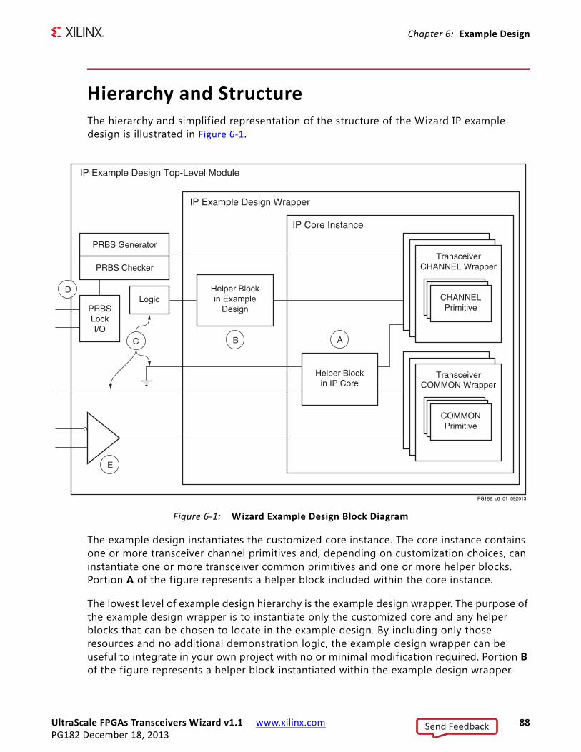
UltraScale FPGAs Transceivers Wizard v1.1 www.xilinx.com 88PG182 December 18, 2013
Chapter 6: Example Design
Hierarchy and StructureThe hierarchy and simplif ied representation of the structure of the Wizard IP example design is illustrated in Figure 6‐1.
The example design instantiates the customized core instance. The core instance contains one or more transceiver channel primitives and, depending on customization choices, can instantiate one or more transceiver common primitives and one or more helper blocks. Portion A of the f igure represents a helper block included within the core instance.
The lowest level of example design hierarchy is the example design wrapper. The purpose of the example design wrapper is to instantiate only the customized core and any helper blocks that can be chosen to locate in the example design. By including only those resources and no additional demonstration logic, the example design wrapper can be useful to integrate in your own project with no or minimal modif ication required. Portion B of the figure represents a helper block instantiated within the example design wrapper.
X-Ref Target - Figure 6-1
Figure 6‐1: Wizard Example Design Block Diagram
IP Example Design Top-Level Module
IP Core Instance
IP Example Design Wrapper
TransceiverCHANNEL Wrapper
CHANNELPrimitive
TransceiverCOMMON Wrapper
COMMONPrimitive
Helper Blockin IP Core
Helper Blockin Example
Design
PRBS Generator
PRBS Checker
LogicPRBSLockI/O
B
D
E
C A
PG182_c6_01_092013
Send Feedback
UltraScale FPGAs Transceivers Wizard v1.1 www.xilinx.com 89PG182 December 18, 2013
Chapter 6: Example Design
Enabled ports of the core instance that do not directly interface to helper block B are routed through to the next level of example design hierarchy.
The example design top-level module instantiates the example design wrapper and is the top-level module of the Vivado IP example project. The top-level module serves many purposes. Portion C of the figure represents the different ways that ports enabled on the core and exposed through the example design wrapper are handled in the example design top-level module. Ports that were optionally enabled or otherwise enabled but are not directly used in the example design are tied off to their appropriate values (per the core customization). A small number of ports that must be driven internally to the example design for purposes of example design operation are driven by some logic function to produce the necessary value. A small number of ports are also connected to the top-level example design I/O.
An example stimulus module and an example checking module are each instantiated for each transceiver channel instance. As shown in portion D of the f igure, these modules include a PRBS block that is customized for data generation or checking as appropriate, as well as a minimal amount of additional logic suff icient to interface to the selected transmitter data encoding and receiver data decoding formats of the transceiver channels.
Note: The example stimulus and example checking modules fundamentally transmit and check raw PRBS data, and do not implement higher-level protocols to encapsulate that raw data.
Because independent example stimulus and checking modules exist per channel, an aggregate pattern match status across all modules is needed. A small amount of logic in the example design top-level module combines the match status from all example checking modules into a single “match all” signal. A sticky error indicator is set any time the “match all” signal deasserts, and an accompanying reset signal clears that sticky error indicator. Together, these three signals are suff icient to monitor data integrity across all transceiver channels in an abstracted fashion, including mapping the top-level I/O to two LEDs and one pushbutton on a PCB.
As shown in portion E of the figure, a dedicated transceiver reference clock differential buffer (IBUFDS_GTE3 primitive) is instantiated for each reference clock source that was specified in the Physical Resources tab of the IP Customization Vivado IDE. Differential clock input ports drive each buffer instance, which in turn is wired to all the transceiver channel or transceiver common primitives it was specif ied to drive. If you wish to use different connectivity in your system, then to properly adjust both the wiring and the transceiver primitive location constraints, re-customize the core and choose different transceiver reference clock locations rather than modifying the clock connectivity.
The ports shown in Table 6-1 are present on the example design top-level module, and are therefore package pins in the example project.
Send Feedback
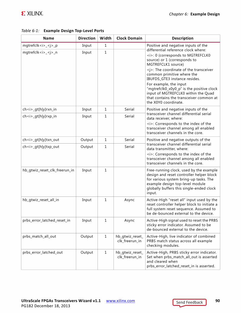
UltraScale FPGAs Transceivers Wizard v1.1 www.xilinx.com 90PG182 December 18, 2013
Chapter 6: Example Design
Table 6‐1: Example Design Top‐Level Ports
Name Direction Width Clock Domain Description
mgtrefclk<i>_<j>_p Input 1 Positive and negative inputs of the differential reference clock where:<i>: 0 (corresponds to MGTREFCLK0 source) or 1 (corresponds to MGTREFCLK1 source)<j>: The coordinate of the transceiver common primitive where the IBUFDS_GTE3 instance resides.For example, the input “mgtrefclk0_x0y0_p” is the positive clock input of MGTREFCLK0 within the Quad that contains the transceiver common at the X0Y0 coordinate.
mgtrefclk<i>_<j>_n Input 1
ch<i>_gt[h|y]rxn_in Input 1 Serial Positive and negative inputs of the transceiver channel differential serial data receiver, where:<i>: Corresponds to the index of the transceiver channel among all enabled transceiver channels in the core.
ch<i>_gt[h|y]rxp_in Input 1 Serial
ch<i>_gt[h|y]txn_out Output 1 Serial Positive and negative outputs of the transceiver channel differential serial data transmitter, where:<i>: Corresponds to the index of the transceiver channel among all enabled transceiver channels in the core.
ch<i>_gt[h|y]txp_out Output 1 Serial
hb_gtwiz_reset_clk_freerun_in Input 1 Free-running clock, used by the example design and reset controller helper block for various system bring-up tasks. The example design top-level module globally buffers this single-ended clock input.
hb_gtwiz_reset_all_in Input 1 Async Active-High “reset all” input used by the reset controller helper block to initiate a full system reset sequence. Assumed to be de-bounced external to the device.
prbs_error_latched_reset_in Input 1 Async Active-High signal used to reset the PRBS sticky error indicator. Assumed to be de-bounced external to the device.
prbs_match_all_out Output 1 hb_gtwiz_reset_clk_freerun_in
Active-High, live indicator of combined PRBS match status across all example checking modules.
prbs_error_latched_out Output 1 hb_gtwiz_reset_clk_freerun_in
Active-High, PRBS sticky error indicator. Set when prbs_match_all_out is asserted and cleared when prbs_error_latched_reset_in is asserted.
Send Feedback
UltraScale FPGAs Transceivers Wizard v1.1 www.xilinx.com 91PG182 December 18, 2013
Chapter 6: Example Design
Convenience FeaturesThe Wizard example design provides several convenience features that can be useful when integrating the core instance into your system.
• Any helper blocks that were specified to be included in the example design are instantiated within the example wrapper level of hierarchy. By including only those resources and no additional demonstration logic, the example design wrapper can be useful to integrate in your own project with no, or minimal modif ication required.
• If the transceiver common was specif ied to be included in the example design, all enabled transceiver common instances are also localized within the example wrapper level of hierarchy.
• As described in Chapter 2, Product Specif ication, the core provides vectored ports that are concatenations of the corresponding port across enabled transceiver primitives. While this provides a compact and predictable user interface, users might prefer individual signals per transceiver primitive. The example design top-level module provides vector slicing for each enabled port, assigning each slice as appropriate for the signal type. This feature can be used for reference or integrated into your system as desired. Three examples follow, for illustration:
a. If the core instance contains four enabled GTH transceiver channels, their GTHTXP serial data output pins are vectored as gthtxp_out[3:0] on the core interface and mapped to gthtxp_int[3:0] within the example design top-level module. The four bits of the vector are sliced into four per-channel assignments that also map to top-level outputs. The “ch” prefix of each signal indicates a transceiver channel signal type, and the number that follows indicates its index among all enabled transceiver channel primitives:
wire [3:0] gthtxp_int;assign ch0_gthtxp_out = gthtxp_int[0:0];assign ch1_gthtxp_out = gthtxp_int[1:1];assign ch2_gthtxp_out = gthtxp_int[2:2];assign ch3_gthtxp_out = gthtxp_int[3:3];
b. If the core instance contains three enabled transceiver channels and optionally enables the drpaddr_in port, the 9-bit DRPADDR transceiver channel ports are vectored as drpaddr_in[26:0] on the core interface and mapped to drpaddr_int[26:0] within the example design top-level module. The 27 bits of the vector are sliced into three per-channel assignments that are each set to the same default driver value that the corresponding transceiver primitive port would have been assigned to internally if the port were not exposed on the core interface. If you choose to integrate the vector slicing convenience code into your project, assign the signals as appropriate for your system:
wire [26:0] drpaddr_int;wire [8:0] ch0_drpaddr_int = 9'b000000000;wire [8:0] ch1_drpaddr_int = 9'b000000000;
Send Feedback
UltraScale FPGAs Transceivers Wizard v1.1 www.xilinx.com 92PG182 December 18, 2013
Chapter 6: Example Design
wire [8:0] ch2_drpaddr_int = 9'b000000000;assign drpaddr_int[8:0] = ch0_drpaddr_int;assign drpaddr_int[17:9] = ch1_drpaddr_int;assign drpaddr_int[26:18] = ch2_drpaddr_int;
c. If the core instance contains one enabled transceiver common and optionally enables the qpll0lock_out port, the one-bit QPLL0LOCK transceiver common port is provided as qpll0lock_out[0:0] on the core interface and mapped to qpll0lock_int[0:0] within the example design top-level module. For this single primitive case, the provided vector slicing is equivalent to a renamed signal. The “cm” prefix of each signal indicates a transceiver common signal type, and the number that follows indicates its index among all enabled transceiver common primitives:
wire [0:0] qpll0lock_int;wire [0:0] cm0_qpll0lock_int;assign cm0_qpll0lock_int = qpll0lock_int [0:0];
d. Multiple instances of a helper block also results in similar assignments. The “hb” prefix of each signal indicates a helper block signal type, and the number that follows indicates its index among all included helper blocks of that type.
Note: A very small number of uncommonly-used transceiver primitive ports are tied off to safe values within the core. If you use the optional port enablement interface to enable access to such a port on the core interface, a warning message with usage instructions is included as a code comment with its vector slicing assignments in the example design top-level module.
• The example design top-level module provides easy access to the reset inputs of the user clocking network helper blocks, and by default, drives them with appropriate signals that indicate clock source stability.
Adapting the Example DesignThe example design is provided as a means of Wizard IP core demonstration, and it can also prove useful as a starting point for integrating the core into your system. While you should not modify core files themselves, modif ication of the example design can be a useful part of this adaptation. However, Xilinx cannot guarantee support for modif ications made to the example design contents as they are delivered, so be sure to understand the effects of your changes and to follow any recommendations in this document and in the example design code.
It can be useful to use the example wrapper level of the example design hierarchy in your system because it instantiates the core and contains the example helper blocks and transceiver common instances if those resources were specified to be located in the example design during IP customization. Helper blocks and transceiver common instances delivered within the example wrapper are provided as examples and can be modif ied as necessary to suit your system requirements.
Send Feedback
UltraScale FPGAs Transceivers Wizard v1.1 www.xilinx.com 93PG182 December 18, 2013
Chapter 6: Example Design
Note: The same parameter overrides exist on transceiver common instances for a given core customization, regardless of their instantiated location.
One or more IBUFDS_GTE3 transceiver differential reference clock buffer primitives are instantiated in the example design top-level module to drive transceiver PLLs as appropriate for your core instance. These buffers as well as any OBUFDS_GTE3 differential recovered clock output buffers are included in the example design rather than the core to facilitate sharing and for general clocking flexibility. However, they are necessary components of the Wizard solution, so the buffer primitives and the nets they connect to should be included in your system. If you wish to use different connectivity in your system, then to properly adjust both the wiring and the transceiver primitive location constraints, re-customize the core and choose different transceiver reference clock and/or recovered clock buffer locations rather than modifying the clock connectivity.
As described in Chapter 5, Constraining the Core, the example design XDC file contains top-level design constraints, some of which will be necessary to include in your system when the Wizard IP core is integrated into it. For example, differential reference clock period constraints and buffer location constraints must be included in your own project XDC file. The core-level XDC file that constrains individual transceiver channel locations and user clocking network clock periods automatically remains associated with each instantiation of the core.
Limitations of the Example DesignThe example design is the recommended means of simulating or implementing an instance of the Wizard IP core outside the context of your own system. It can also prove useful as a starting point for integrating the core into your system. However, it is quite simplistic, and the following limitations should be understood:
• The example design does not implement specif ic protocols to generate or check data. For example, while the example stimulus module does support TX Gearbox data encoding configurations and the example checking module does support RX Gearbox data decoding configurations to interface to the transceiver channel primitives, they do not implement true 64B/66B or 64B/67B data coding. Fundamentally, raw PRBS data is generated and checked.
• When the example design is simulated using the provided test bench, each transceiver channel is looped back from the serial data transmitter to the receiver. As such, data integrity can only be properly checked if the transmitter and receiver are configured for the same line rate and to use the same data coding. No transcoding or rate adjustment schemes are used. If the transmitter and receiver line rates or data coding are configured differently from one another in your system, you might wish to cross-couple two appropriately-customized core instances and check for data integrity in hardware or in your own test bench. In such a setup, the transmitter of core instance A is rate- and coding-matched to the receiver of core instance B, and vice versa.
Send Feedback
UltraScale FPGAs Transceivers Wizard v1.1 www.xilinx.com 94PG182 December 18, 2013
Chapter 6: Example Design
• The example design PRBS match logic is not resilient to bit errors, nor does it record a bit error ratio. The occurrence of even one error after lock is achieved causes the sticky error indicator to be asserted, and potentially for the example checking logic to search for proper PRBS match and data alignment, which can take some time.
Send Feedback
UltraScale FPGAs Transceivers Wizard v1.1 www.xilinx.com 95PG182 December 18, 2013
Chapter 7
Test BenchThis chapter contains information about the provided test bench in the Vivado® Design Suite.
The UltraScale™ FPGAs Transceivers Wizard includes a simple self-checking test bench module that provides basic stimulus to the example design and interacts with its PRBS lock I/O to check for data integrity across all enabled transceiver channels.
Simulating the Example DesignTo simulate an instance of the Wizard IP core, f irst open its example design as described in Chapter 6, Example Design. In the example project, start a behavioral simulation by clicking Run Simulation > Run Behavioral Simulation in the Vivado IDE. The Simulation Settings selection can be used to choose the supported simulator of your choice.
The example design instantiates an example stimulus module to drive the transmitter user interface and an example checking module that is driven by the receiver user interface of each transceiver channel. The example design combines the individual PRBS match indicators from each channel into an overall match signal with corresponding sticky error indicator and dedicated reset input. See Chapter 6, Example Design for more details on the data stimulus and checking functions of the example design.
The provided test bench instantiates the example design top-level module and loops back each enabled transceiver channel in the core instance from the serial data transmitter to the receiver. This enables the example stimulus and checking modules within the example design to operate as part of a self-checking system under the stimulus of the simulation test bench. For more information, refer to Vivado Design Suite: Logic Simulation (UG900) [Ref 5].
Send Feedback
UltraScale FPGAs Transceivers Wizard v1.1 www.xilinx.com 96PG182 December 18, 2013
Chapter 7: Test Bench
Simulation BehaviorThe example design simulation test bench provides the requisite free-running clock and transceiver reference clock signals, as well as a “reset all” pulse to the reset controller helper block input ports. This stimulus is suff icient to allow the helper blocks to bring up the remainder of the system. After some time, the transceiver PLL(s) will achieve lock, allowing the reset controller helper block f inite state machines to complete the full reset sequence. After the reset sequence is complete, you can begin to observe the example stimulus module transmitting data. A short time later, the example checking module begins to search for data alignment and checks for data integrity.
The example design output port prbs_match_all_out indicates a PRBS match across all channels. The test bench uses a counter to detect a level prbs_match_all_out assertion, and deassertions reset the counter. When the counter saturates, PRBS lock is declared. When the test bench f irst detects PRBS lock, it prints this message to the transcript:
Initial PRBS lock achieved across all transceiver channels
The test bench then pulses prbs_error_latched_reset_in to reset the example design sticky error indicator, and allows the simulation to run for a prescribed period of time to ensure that PRBS lock is maintained. These messages are printed to the transcript:
Resetting latched PRBS error indicator.
Continuing simulation for 50us to check for maintenance of lock and error-free operation.
At the end of the prescribed wait period, the test bench checks whether PRBS lock has been maintained. If so, the following messages are printed to the transcript and the test is considered to have passed. The simulation then f inishes:
PASS: simulation completed with maintained PRBS lock and error-free operation.
** Test completed successfully
Figure 7-1 shows the characteristic waveform of a passing test, demonstrating initial and transient PRBS matches, a saturating PRBS lock counter leading to the lock indicator, a pulse to reset the sticky error indicator, and the beginning of the wait period where the test bench is run while the sticky error indicator remains deasserted. The signals shown are those from the test bench level of hierarchy only, and are the default set when loading a simulation from the Vivado design tools. You might wish to add additional signals to the waveform window for more visibility into the operation of the example design or the core instance.
Send Feedback
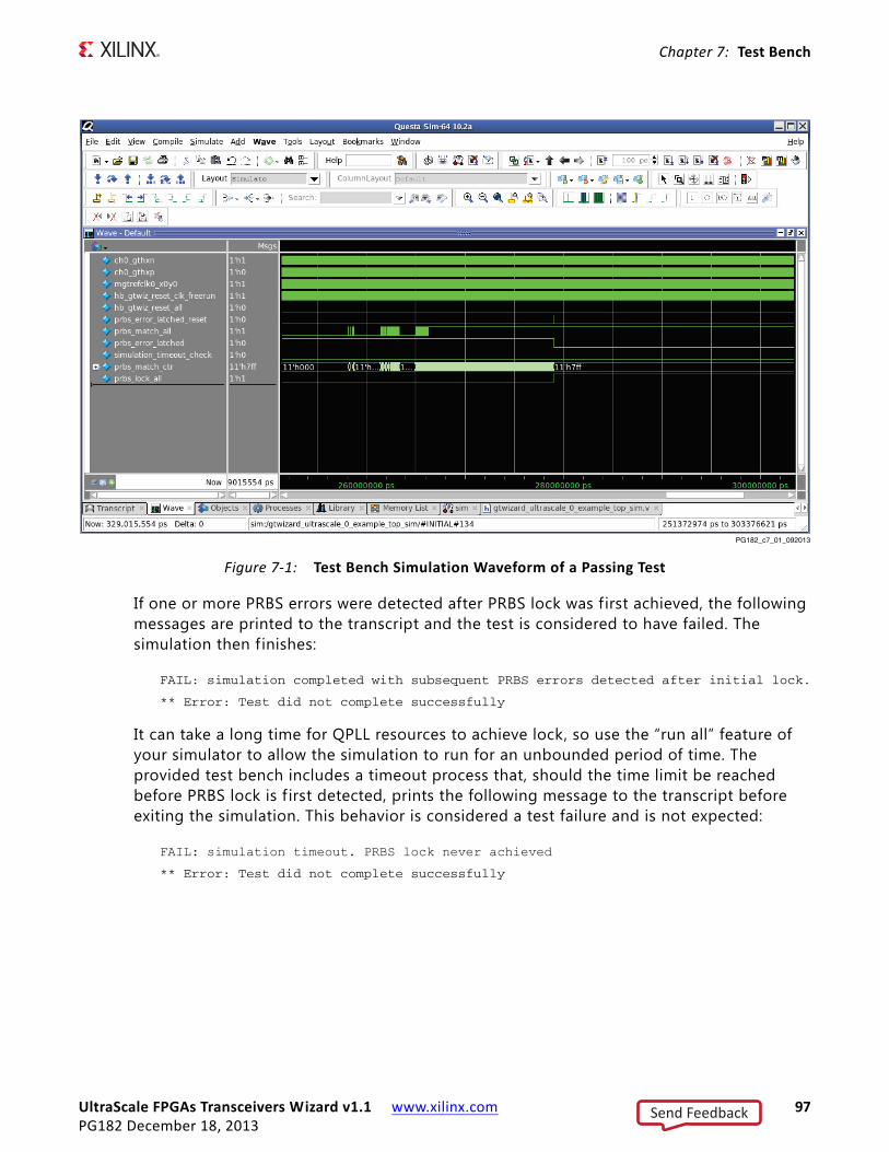
UltraScale FPGAs Transceivers Wizard v1.1 www.xilinx.com 97PG182 December 18, 2013
Chapter 7: Test Bench
If one or more PRBS errors were detected after PRBS lock was first achieved, the following messages are printed to the transcript and the test is considered to have failed. The simulation then finishes:
FAIL: simulation completed with subsequent PRBS errors detected after initial lock.
** Error: Test did not complete successfully
It can take a long time for QPLL resources to achieve lock, so use the “run all” feature of your simulator to allow the simulation to run for an unbounded period of time. The provided test bench includes a timeout process that, should the time limit be reached before PRBS lock is f irst detected, prints the following message to the transcript before exiting the simulation. This behavior is considered a test failure and is not expected:
FAIL: simulation timeout. PRBS lock never achieved
** Error: Test did not complete successfully
X-Ref Target - Figure 7-1
Figure 7‐1: Test Bench Simulation Waveform of a Passing Test
PG182_c7_01_092013
Send Feedback
UltraScale FPGAs Transceivers Wizard v1.1 www.xilinx.com 98PG182 December 18, 2013
Appendix A
Migrating and UpgradingThis appendix contains information about migrating a design from ISE® to the Vivado® Design Suite, and for upgrading to a more recent version of the IP core. For customers upgrading in the Vivado Design Suite, important details (where applicable) about any port changes and other impact to user logic are included.
Migrating to the Vivado Design SuiteFor information about migrating to the Vivado Design Suite, see the ISE to Vivado Design Suite Migration Guide (UG911) [Ref 6].
Upgrading from a Previous VersionUsers of a prior version of the UltraScale™ FPGAs Transceivers Wizard IP core are encouraged to upgrade to the newest version for compatibility and the benefit of any feature enhancements or bug f ixes. Refer to the Wizard core changelog for a record of versions and their specif ic changes.
Migrating from a Previous Device FamilyThere is no direct upgrade path from Transceivers Wizard IP cores for previous Xilinx device families to the UltraScale FPGAs Transceivers Wizard. It is necessary to customize and generate a new core instance when targeting an UltraScale FPGA for the first time.
The Wizard provides a familiar IP Customization Vivado IDE with many of the same options present in previous Xilinx Wizards IP cores, as well as signif icant new features and flexibility.
Send Feedback
UltraScale FPGAs Transceivers Wizard v1.1 www.xilinx.com 99PG182 December 18, 2013
Appendix B
DebuggingThis appendix includes details about resources available on the Xilinx Support website and debugging tools.
Finding Help on Xilinx.comTo help in the design and debug process when using the UltraScale™ FPGAs Transceivers Wizard, the Xilinx Support web page (www.xilinx.com/support) contains key resources such as product documentation, release notes, answer records, information about known issues, and links for obtaining further product support.
Documentation
This product guide is the main document associated with the Wizard. This guide, along with documentation related to all products that aid in the design process, can be found on the Xilinx Support web page (www.xilinx.com/support) or by using the Xilinx Documentation Navigator.
Download the Xilinx Documentation Navigator from the Design Tools tab on the Downloads page (www.xilinx.com/download). For more information about this tool and the features available, open the online help after installation.
Answer Records
Answer Records include information about commonly encountered problems, helpful information on how to resolve these problems, and any known issues with a Xilinx product. Answer Records are created and maintained daily ensuring that users have access to the most accurate information available.
Answer Records for this core can also be located by using the Search Support box on the main Xilinx support web page. To maximize your search results, use proper keywords such as
• Product name
• Tool message(s)
Send Feedback
UltraScale FPGAs Transceivers Wizard v1.1 www.xilinx.com 100PG182 December 18, 2013
Appendix B: Debugging
• Summary of the issue encountered
A filter search is available after results are returned to further target the results.
Master Answer Record for the UltraScale FPGAs Transceivers Wizard
AR: 57487
Contacting Technical Support
Xilinx provides technical support at www.xilinx.com/support for this LogiCORE™ IP product when used as described in the product documentation. Xilinx cannot guarantee timing, functionality, or support of product if implemented in devices that are not defined in the documentation, if customized beyond that allowed in the product documentation, or if changes are made to any section of the design labeled DO NOT MODIFY.
To contact Xilinx Technical Support:
1. Navigate to www.xilinx.com/support.
2. Open a WebCase by selecting the WebCase link located under Additional Resources.
When opening a WebCase, include:
• Target FPGA including package and speed grade.
• All applicable Xilinx Design Tools and simulator software versions.
• Additional f iles based on the specif ic issue might also be required. See the relevant sections in this debug guide for guidelines about which f ile(s) to include with the WebCase.
Note: Access to WebCase is not available in all cases. Login to the WebCase tool to see your specif ic support options.
Vivado Lab ToolsVivado® lab tools insert logic analyzer and virtual I/O cores directly into your design. Vivado lab tools allow you to set trigger conditions to capture application and integrated block port signals in hardware. Captured signals can then be analyzed. This feature represents the functionality in the Vivado IDE that is used for logic debugging and validation of a design running in Xilinx devices in hardware.
Send Feedback
UltraScale FPGAs Transceivers Wizard v1.1 www.xilinx.com 101PG182 December 18, 2013
Appendix B: Debugging
The Vivado logic analyzer is used to interact with the logic debug LogiCORE IP cores, including:
• ILA 2.0 (and later versions)
• VIO 2.0 (and later versions)
See the Vivado Design Suite User Guide: Programming and Debugging (UG908) [Ref 7].
Send Feedback
UltraScale FPGAs Transceivers Wizard v1.1 www.xilinx.com 102PG182 December 18, 2013
Appendix C
Additional Resources
Xilinx ResourcesFor support resources such as Answers, Documentation, Downloads, and Forums, see the Xilinx Support website at:
www.xilinx.com/support.
For a glossary of technical terms used in Xilinx documentation, see:
www.xilinx.com/company/terms.htm.
ReferencesThese documents provide supplemental material useful with this product guide:
1. UltraScale FPGAs GTH Transceivers User Guide (UG576)
2. Kintex UltraScale Architecture Data Sheet: DC and AC Switching Characteristics (DS892)
3. Vivado Design Suite User Guide: Designing with IP (UG896)
4. Vivado Design Suite User Guide: Getting Started (UG910)
5. Vivado Design Suite: Logic Simulation (UG900)
6. Vivado Design Suite Migration Methodology Guide (UG911)
7. Vivado Design Suite User Guide: Programming and Debugging (UG908)
Send Feedback

UltraScale FPGAs Transceivers Wizard v1.1 www.xilinx.com 103PG182 December 18, 2013
Appendix C: Additional Resources
Revision HistoryThe following table shows the revision history for this document.
Notice of DisclaimerThe information disclosed to you hereunder (the “Materials”) is provided solely for the selection and use of Xilinx products. To the maximum extent permitted by applicable law: (1) Materials are made available “AS IS” and with all faults, Xilinx hereby DISCLAIMS ALL WARRANTIES AND CONDITIONS, EXPRESS, IMPLIED, OR STATUTORY, INCLUDING BUT NOT LIMITED TO WARRANTIES OF MERCHANTABILITY, NON-INFRINGEMENT, OR FITNESS FOR ANY PARTICULAR PURPOSE; and (2) Xilinx shall not be liable (whether in contract or tort, including negligence, or under any other theory of liability) for any loss or damage of any kind or nature related to, arising under, or in connection with, the Materials (including your use of the Materials), including for any direct, indirect, special, incidental, or consequential loss or damage (including loss of data, profits, goodwill, or any type of loss or damage suffered as a result of any action brought by a third party) even if such damage or loss was reasonably foreseeable or Xilinx had been advised of the possibility of the same. Xilinx assumes no obligation to correct any errors contained in the Materials or to notify you of updates to the Materials or to product specifications. You may not reproduce, modify, distribute, or publicly display the Materials without prior written consent. Certain products are subject to the terms and conditions of Xilinx’s limited warranty, please refer to Xilinx’s Terms of Sale which can be viewed at http://www.xilinx.com/legal.htm#tos; IP cores may be subject to warranty and support terms contained in a license issued to you by Xilinx. Xilinx products are not designed or intended to be fail-safe or for use in any application requiring fail-safe performance; you assume sole risk and liability for use of Xilinx products in such critical applications, please refer to Xilinx’s Terms of Sale which can be viewed at http://www.xilinx.com/legal.htm#tos.© Copyright 2013 Xilinx, Inc. Xilinx, the Xilinx logo, Artix, ISE, Kintex, Spartan, Virtex, UltraScale, Vivado, Zynq, and other designated brands included herein are trademarks of Xilinx in the United States and other countries. All other trademarks are the property of their respective owners.
Date Version Revision
12/18/2013 1.1 Initial Xilinx release.
Send Feedback