Combination of nanophotonic biosensors and light-assisted ...

Approved for Public Release, Distribution Unlimited
Ultraperformance Nanophotonic Intrachip Communications: UNÍC
Ultraperformance Nanophotonic Intrachip Ultraperformance Nanophotonic Intrachip Communications: UNCommunications: UNÍÍC C
Jagdeep ShahDARPA/MTO
Jagdeep ShahDARPA/MTO
Frontiers of Extreme Computing 2007Santa Cruz, CA
October 21-24, 2007

Slide 2Frontiers of Extreme Computing 2007: Santa Cruz, CA
Approved for Public Release, Distribution Unlimited
UNÍC: OutlineUNUNÍÍC: OutlineC: Outline
• Introduction: Vision and Challenges• Microprocessor Challenges
• Photonics/EPIC • UNÍC
• Summary

Slide 3Frontiers of Extreme Computing 2007: Santa Cruz, CA
Approved for Public Release, Distribution Unlimited
CHALLENGE AND VISIONCHALLENGE AND VISIONCHALLENGE AND VISION

Slide 4Frontiers of Extreme Computing 2007: Santa Cruz, CA
Approved for Public Release, Distribution Unlimited
DEVICE SCALINGMICROPROCESSOR SCALING
DEVICE SCALINGDEVICE SCALINGMICROPROCESSOR SCALINGMICROPROCESSOR SCALING
Intel Itanium 2 (2006)1.72 billion transistors, 596 mm2
~300,000,000 transistors/cm2
The Impact of Moore’s Law:• Device scaling most obvious in microprocessors• On the path to >> 1 billion devices/ cm2
• 3D layer stacking on all foundry roadmapsMicroprocessors are becoming
Ultradense Systems
Intel 4004 (1971)2312 transistors, 11 mm2
~20,000 transistors/cm2
15,000 X Increase in Device Density
DARPA/MTO VISA Program

Slide 5Frontiers of Extreme Computing 2007: Santa Cruz, CA
Approved for Public Release, Distribution Unlimited
Other Ultradense systemsOther Ultradense systemsOther Ultradense systems
DARPA MoleApps – Aim: 1015 devices/ cm3
Courtesy HP
17 nm half-pitch,3.5*1011 /cm2
demonstrated

Slide 6Frontiers of Extreme Computing 2007: Santa Cruz, CA
Approved for Public Release, Distribution Unlimited
CHALLENGECHALLENGE•• How will these ultradense functional units How will these ultradense functional units communicatecommunicate–– With each other?With each other?–– With the external world?With the external world?
VISIONDEVELOP A PATHWAY FOR SUCH COMMUNICATIONS
CHALLENGE AND VISIONCHALLENGE AND VISIONCHALLENGE AND VISION

Slide 7Frontiers of Extreme Computing 2007: Santa Cruz, CA
Approved for Public Release, Distribution Unlimited
UNÍC: Ultraperformance Nanophotonic Intrachip Communications
UNUNÍÍC: Ultraperformance Nanophotonic C: Ultraperformance Nanophotonic Intrachip CommunicationsIntrachip Communications
•DARPA is about to launch a program to develop such a pathway:
• for communications between ultrahigh functional units on a chip and from the chip to the outside world
•Enormous challenges: Focus on a specific challenge of microprocessors
•Use microprocessor circa 2017 as a design driver

Slide 8Frontiers of Extreme Computing 2007: Santa Cruz, CA
Approved for Public Release, Distribution Unlimited
MICROPROCESSOR CHALLENGESMICROPROCESSOR CHALLENGESMICROPROCESSOR CHALLENGES

Slide 918th Annual Workshop: Interconnections within High-Speed Digital Systems, Santa Fe, NM
Approved for Public Release, Distribution Unlimited
1.00E-04
1.00E-02
1.00E+00
1.00E+02
1.00E+04
1.00E+06
1.00E+08
1980 1990 2000 2010 2020
Perf (ps/Inst)Delay/CPUs
X86 (52%/yr)Moore’s Law (74%/year)
19%/year30:1
30,000:1Source: ISAT Summer 2001 Study; Prof. Bill Dally (Stanford) Study Lead
We’re already seeing this effect:
Diminishing Performance Returns Diminishing Performance Returns
Microprocessor performance is not keeping pace with device scaling due to limitations at the circuit level
• Diminishing returns of ILP• Thermal constraints• Increasing complexity• Growing communications gap
System-level balance• Memory/ Bisection-Bandwidth balancedagainst peak performance
Metric: Bytes/FLOP ([B/s]/[FLOPS]) ~1• On-chip/ off-chip bandwidth balanced• Power Consumption
Uniform Distribution: 1/3 Processing, 1/3 Communications, 1/3 Memory
Supercomputer Comms Gap• Memory and bisection bandwidth imbalance a growing problem
• Limited by power consumption
Example: Cray XT4, 380 TFBytes/Flop ~0.06
Communications challenges prevent actual system performance from meeting theoretical peak performance

Slide 1018th Annual Workshop: Interconnections within High-Speed Digital Systems, Santa Fe, NM
Approved for Public Release, Distribution Unlimited
Multicore ProcessorsToday and TomorrowMulticore ProcessorsToday and Tomorrow
IBM
Cel
l
Sun
Nia
gara
Inte
l Pol
aris
“Supercomputers on-Chip”
1 TFLOPS on-chip reported
• Processor/On-chip Memory–100-1000 compute cores in ~6 cm2
–~10 TFLOPS peak performance–3D-integration–>100 billion active devices!
• Required Communications Network–~80 Tb/s on-chip bandwidth–~80 Tb/s off-chip memory BW
• Total System Power ~200 W
Multicore ProcessorPlane
3D Integration
• Reducing system-level power consumption• High-bandwidth, low-power access to
ultradense devices• The communications gap:
– Latency/Bandwidth limits– Power dissipation as wires shrink– Power-hungry off-chip communications
to memory
Electronics cannot meet communication requirements within power budget. Actual performance cannot meet theoretical peak performance.
A new communications strategy is required
Challenges
Multicore architectures designed to deliver increased performance
at the circuit level
Glo
bal I
nfor
mat
ion
Grid
: 5 T
b/s

Slide 1118th Annual Workshop: Interconnections within High-Speed Digital Systems, Santa Fe, NM
Approved for Public Release, Distribution Unlimited
PHOTONICSPHOTONICS
Slide 12Frontiers of Extreme Computing 2007: Santa Cruz, CA
Approved for Public Release, Distribution Unlimited
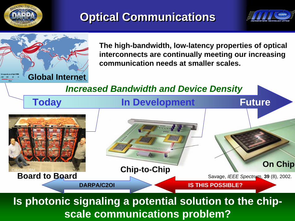
Optical CommunicationsOptical Communications
On ChipChip-to-Chip
Today In Development FutureIncreased Bandwidth and Device Density
Is photonic signaling a potential solution to the chip-scale communications problem?
DARPA/C2OIBoard to Board
The high-bandwidth, low-latency properties of optical interconnects are continually meeting our increasing communication needs at smaller scales.
Courtesy: IBM
IS THIS POSSIBLE?
Global Internet
Savage, IEEE Spectrum, 39 (8), 2002.

Slide 13Frontiers of Extreme Computing 2007: Santa Cruz, CA
Approved for Public Release, Distribution Unlimited
PHOTONICSPHOTONICSPHOTONICS
BENEFITS• High Bandwidth/Capacity
– Wavelength Division Multiplexing (WDM)– Time Division Multiplexing (TDM)– Space Division Multiplexing (SDM)
• No need for power hungry repeaters• Power Independent Of Distance ( ~ 10 cm)• Seamless I/O
CHALLENGES• Compatibility with Silicon• Current devices too large: can they be scaled down in size? • Current devices are power hungry: can the power be reduced?• Spectral bandwidth vs. thermal stability
Devices required to meet these challenges will be very different from today’s devices performing the same functions

Slide 14Frontiers of Extreme Computing 2007: Santa Cruz, CA
Approved for Public Release, Distribution Unlimited
EPICELECTRONIC PHOTONIC INTEGRATED CIRCUITS
EPICEPICELECTRONIC PHOTONIC ELECTRONIC PHOTONIC INTEGRATED CIRCUITSINTEGRATED CIRCUITS
Success of EPIC gives confidence
that this is possible
Success of EPIC gives Success of EPIC gives confidence confidence
that this is possiblethat this is possible

Slide 15Frontiers of Extreme Computing 2007: Santa Cruz, CA
Approved for Public Release, Distribution Unlimited
EPICEPICEPIC
• Legacy microphotonic devices were discrete components using a variety of materials
• Moore’s law has opened the way for integrated photonics in Si• High index-contrast of Si/SiO2 and smooth features below 90nm
node enable nanophotonic devices• DARPA EPIC Program has demonstrated high performance,
monolithically integrated photonic and electronic devices using a standard CMOS foundry
• Application-specific EPIC chips demonstrated

Slide 16Frontiers of Extreme Computing 2007: Santa Cruz, CA
Approved for Public Release, Distribution Unlimited
UNÍCUNUNÍÍCC
PHOTONICALLY-ENABLED MICROPROCESSOR
PHOTONICALLYPHOTONICALLY--ENABLED ENABLED MICROPROCESSORMICROPROCESSOR

Slide 17Frontiers of Extreme Computing 2007: Santa Cruz, CA
Approved for Public Release, Distribution Unlimited
UNÍC APPROACHUNUNÍÍC APPROACHC APPROACH
• Select a Design Driver (with ultradense functional units: microprocessor circa 2017)
• Design a photonic communication network within the constraints imposed by the design driver
• Quantify the system benefits of the approach• Quantify device requirements to enable such
communications• Demonstrate the required device performance• Demonstrate on-chip functional communication links
with all essential components working in unison(sufficiently aggressive to convince the skeptics)
• Demonstrate multiple high performance microprocessors communicating via on-chip optical links

18 Slide 1818th Annual Workshop: Interconnections within High-Speed Digital Systems, Santa Fe, NMApproved for Public Release, Distribution Unlimited
UNÍC: OBJECTIVE UNÍC: OBJECTIVE
Comprehensive, team-based efforts encompassing
1.Photonic Communication Architecture (on/off chip) 2.Device demonstrations (compatible with CMOS fabs) far beyond EPIC 3.System-level performance-benefit analysis4.Full-link demonstrations of all critical technologies working together; application emulation5.Microprocessors communicating via on-chip optical linkes
IntegratedDemos
SystemBenefit
Analysis
Photonic CommsArchitecture
AggressiveDevice
Development
1
4
2 3
No effort on processor design, architecture…
Demonstrate to the microprocessor community (and others) that photonic intra-chip – and seamless off-chip – communication is a
credible technology that will allow actual system performance to scale to a level not possible with electronic communications

Slide 19Frontiers of Extreme Computing 2007: Santa Cruz, CA
Approved for Public Release, Distribution Unlimited
Optical Link Key ComponentsOptical Link Key ComponentsOptical Link Key Components
Laser
Electrical InputFrom Processor
CoreElectrical
OutputOn-Chip Network/
Switching
Optical Link Example
How can 80 Tb/s be achieved?•Transmit – Spatial Division Multiplexing (SDM) and Wave Division Multiplexing (WDM) of optical signals with multiple, low-insertion-loss, high-BW modulators
• Route – Spectrally filtered passive networks or active, arbitrated spatial switch networks using low loss, high power handling waveguides. Power consumption due to tuning must be kept at a minimum by using thermally tolerant designs.
• Receive – High-BW, high-responsivity, low-power (no TIA) photo detectors
Transmit Route Receive
Link Energy ~100 fJ/bit
Modulators
Waveguides
SDM
Core A Core B
……
Filters
Detectors
WDM

Slide 20Frontiers of Extreme Computing 2007: Santa Cruz, CA
Approved for Public Release, Distribution Unlimited
Photonic Device ChallengesPhotonic Device ChallengesPhotonic Device Challenges
System-level constraints mandate stringent performance requirements
Next Generation Intra-chip Communication Devices Require Dramatic Size and Power Reductions
Device Example (w/drivers)
EPICDemonstrated
UNÍCRequirements
RequiredImprovement
Area
Power
Area 0.6 mm2 0.005 mm2 120 X
Power
Area
Power
700 μm2 28 μm2 25 X0.8 mW330 mW
73 mW (tuning)
0.16 mm2
36 mW
0 mW ?
0.01 mm2
1 mW
10+ Gb/s Modulator825 X
WDM Filter???
16X10+ Gb/s Detector
36 X
UNÍC will consist of many EPIC-like circuits with dramatically reduced power consumption and dimensionsEPIC
UNÍC

Slide 21Frontiers of Extreme Computing 2007: Santa Cruz, CA
Approved for Public Release, Distribution Unlimited
Potential BenefitsPotential BenefitsPotential Benefits
System-level benefits– Restores B/F system balance to maximize actual performance– Facilitates architectures which reduce programming complexity
(e.g. shared memory)– Reduces chip and system power– Enables deployable, chip-scale supercomputers
Image Processing SAR Processing Cryptanalysis
PHOTONIC TECHNOLOGY BENEFITS• High Bandwidth: Wavelength, Time, and Space Division Multiplexing• Low Power: No repeaters, buffers, regenerators; independent of dist.• Seamless I/O: No need for power-hungry off-chip communication• Enables high performance for low system power
Autonomous Ops
Real-Time, High-Performance Embedded Processing Supercomputers

Slide 22Frontiers of Extreme Computing 2007: Santa Cruz, CA
Approved for Public Release, Distribution Unlimited
SUMMARYSUMMARYSUMMARY
• Device scaling is producing ultradense electrical microsystems
• Microprocessors are becoming ultradense supercomputers on-chip
• High-performance computer systems are becoming unbalanced due to communications bottleneck
• Photonic communications may provide a novel solution to high BW on- and off-chip communications challenges
• UNIC addresses this problem head-on