Ultrafast dynamics in semiconductor devices
113
ULTRAFAST DYNAMICS IN SEMICONDUCTOR DEVICES by Botao Zhang B.S., University of Science and Technology of China, 2003 M.S., University of Pittsburgh, 2005 Submitted to the Graduate Faculty of the Department of Physics & Astronomy in partial fulfillment of the requirements for the degree of Doctor of Philosophy University of Pittsburgh 2010
Transcript of Ultrafast dynamics in semiconductor devices

ULTRAFAST DYNAMICS IN SEMICONDUCTOR
DEVICES
by
Botao Zhang
B.S., University of Science and Technology of China, 2003
M.S., University of Pittsburgh, 2005
Submitted to the Graduate Faculty of
the Department of Physics & Astronomy in partial fulfillment
of the requirements for the degree of
Doctor of Philosophy
University of Pittsburgh
2010

UNIVERSITY OF PITTSBURGH
DEPARTMENT OF PHYSICS & ASTRONOMY
This dissertation was presented
by
Botao Zhang
It was defended on
October 2010
and approved by
David W. Snoke, Department of Physics & Astronomy
Jeremy Levy, Department of Physics & Astronomy
Kevin P. Chen, Department of Electrical and Computer Engineering
Rob D. Coalson, Department of Chemistry
Vladimir Savinov, Department of Physics & Astronomy
Dissertation Director: David W. Snoke, Department of Physics & Astronomy
ii
ULTRAFAST DYNAMICS IN SEMICONDUCTOR DEVICES
Botao Zhang, PhD
University of Pittsburgh, 2010
This research focuses on three type of GaAs-based semiconductor devices, namely oxide-
confined vertical-cavity surface-emitting lasers (VCSEL), GaAs/AlGaAs quantum dots and
GaAs microdisk lasers. An individual transverse mode distribution in a VCSEL has been
resolved by a scanning confocal microscope in connection with an optical spectrum analyzer.
With resonant femtosecond (fs) pulse injection, we directly perturb the cavity field of a
VCSEL. After the injection, the lasing and nonlasing mode dynamics are measured. Spatio-
temporal resolution of the VCSEL’s modes helps us to understand how to lock transverse
modes and work toward a new type of mode-locked pulse laser. By injecting cross-polarized
laser pulses into a VCSEL cavity, we also studied the ultrafast polarization effects of a
single-mode VCSEL. Based on time-resolved microscopic photoluminescence (µPL) from
single self-assembled GaAs/AlGaAs quantum dots, we unambiguously identify one of the
emission lines as arising from positive trions (two holes and one electron) in these nominally
undoped quantum dots. The trion is formed via tunneling of one electron out of the dot after
optical excitation of a biexciton. The rise time of the trion emission line matches the decay
time of the biexciton due to electron tunneling. Time-resolved whispering-gallery modes
(WGMs) of GaAs microdisk lasers show a red-shift in time. After the fs laser pulse pump,
there is a turn-on delay of the microdisk laser lasing emission. With the increasing pump
power, the WGMs shift to shorter wavelength.
iii

TABLE OF CONTENTS
PREFACE . . . . . . . . . . . . . . . . . . . . . . . . . . . . . . . . . . . . . . . . . xi
1.0 INTRODUCTION . . . . . . . . . . . . . . . . . . . . . . . . . . . . . . . . . 1
1.1 Overview . . . . . . . . . . . . . . . . . . . . . . . . . . . . . . . . . . . . . 1
1.2 Semiconductors . . . . . . . . . . . . . . . . . . . . . . . . . . . . . . . . . 2
1.2.1 Semiconductor Optics . . . . . . . . . . . . . . . . . . . . . . . . . . 4
1.2.2 Semiconductor Heterostructures . . . . . . . . . . . . . . . . . . . . . 9
1.3 Quantum Dots . . . . . . . . . . . . . . . . . . . . . . . . . . . . . . . . . . 14
1.4 Semiconductor Diode Lasers . . . . . . . . . . . . . . . . . . . . . . . . . . 15
1.4.1 The Principle of Operation . . . . . . . . . . . . . . . . . . . . . . . . 15
1.4.2 Vertical-cavity Surface-emitting Lasers . . . . . . . . . . . . . . . . . 16
2.0 EXPERIMENTAL SETUP . . . . . . . . . . . . . . . . . . . . . . . . . . . 21
2.1 Optical Spectroscopy . . . . . . . . . . . . . . . . . . . . . . . . . . . . . . 21
2.2 Ti:Sapphire Lasers . . . . . . . . . . . . . . . . . . . . . . . . . . . . . . . . 22
2.2.1 Why Ti:Sapphire crystal? . . . . . . . . . . . . . . . . . . . . . . . . 22
2.2.2 Producing ultrafast pulses . . . . . . . . . . . . . . . . . . . . . . . . 23
2.2.2.1 Q-switching . . . . . . . . . . . . . . . . . . . . . . . . . . . . 23
2.2.2.2 Mode-locking . . . . . . . . . . . . . . . . . . . . . . . . . . . 25
2.2.3 Dispersion compensation . . . . . . . . . . . . . . . . . . . . . . . . . 31
2.2.4 Ti:Sapphire laser oscillator design . . . . . . . . . . . . . . . . . . . . 34
2.3 Pulse Shaping . . . . . . . . . . . . . . . . . . . . . . . . . . . . . . . . . . 41
2.3.1 Actively stabilized double pulse generation . . . . . . . . . . . . . . . 41
2.3.2 Double-color double pulse generation . . . . . . . . . . . . . . . . . . 44
iv
2.3.3 Pulse measurements . . . . . . . . . . . . . . . . . . . . . . . . . . . 48
2.4 Time-Resolved Experiment Setups . . . . . . . . . . . . . . . . . . . . . . . 49
2.4.1 ULTRAFAST NONLINEAR OPTICAL SAMPLING OSCILLOSCOPE 49
2.4.2 Streak Camera . . . . . . . . . . . . . . . . . . . . . . . . . . . . . . 54
3.0 QUANTUM DOTS . . . . . . . . . . . . . . . . . . . . . . . . . . . . . . . . 58
3.1 Trion Formation In GaAs-AlGaAs Quantum Dots By Tunneling . . . . . . 58
3.2 Rabi Oscillations . . . . . . . . . . . . . . . . . . . . . . . . . . . . . . . . . 65
4.0 VCSEL MODES . . . . . . . . . . . . . . . . . . . . . . . . . . . . . . . . . . 72
4.1 Transverse-Modes And Mode-Locking . . . . . . . . . . . . . . . . . . . . . 72
4.2 Ultrafast Switching Dynamics of Nonlasing Modes of Vertical-Cavity Surface-
Emitting Lasers . . . . . . . . . . . . . . . . . . . . . . . . . . . . . . . . . 79
5.0 CONCLUSIONS AND FUTURE WORK . . . . . . . . . . . . . . . . . . 87
APPENDIX. MICRODISK LASER . . . . . . . . . . . . . . . . . . . . . . . . . 89
A.1 Whipering Gallery Modes . . . . . . . . . . . . . . . . . . . . . . . . . . . . 89
A.2 Time Dependent Measurements . . . . . . . . . . . . . . . . . . . . . . . . 92
BIBLIOGRAPHY . . . . . . . . . . . . . . . . . . . . . . . . . . . . . . . . . . . . 95
v

LIST OF FIGURES
1 The Brillouin zones. . . . . . . . . . . . . . . . . . . . . . . . . . . . . . . . . 3
2 (a) Face-centered cubic bravis lattice. (b) GaAs lattice. The images are taken
from Ref. [1] . . . . . . . . . . . . . . . . . . . . . . . . . . . . . . . . . . . . 5
3 (a) The first Brillouin zone of fcc lattice; (b) Calculated electron energy band
structure of GaAs [2] . . . . . . . . . . . . . . . . . . . . . . . . . . . . . . . 6
4 The schematic band structure of GaAs around Brillouin zone center. . . . . . 6
5 Direct transition and indirect transition. . . . . . . . . . . . . . . . . . . . . . 7
6 (a) Density of states g(E) for semiconductor in the 3D case; (b) Fermi-Dirac
distribution for electron; (c) Number of quasi-particles per energy dN/dE. . . 8
7 (a) A simple band structure for p-doped and n-doped semiconductor. (b) The
band structure for p-n junction. . . . . . . . . . . . . . . . . . . . . . . . . . 10
8 Heterojunction between two different undoped semiconductor materials. . . . 11
9 GaAs/AlGaAs quantum well band structure. . . . . . . . . . . . . . . . . . . 11
10 The schematics of density of states for 2D electron gas, where the dotted lines
are for 3D case. . . . . . . . . . . . . . . . . . . . . . . . . . . . . . . . . . . 13
11 GaAs/AlGaAs superlattice band structure. . . . . . . . . . . . . . . . . . . . 13
12 Schematics of the density of states in 3D, 2D, 1D and 0D cases. . . . . . . . . 14
13 The double-heterostructure of a diode laser. . . . . . . . . . . . . . . . . . . . 16
14 The schematics of an edge-emitting diode laser. . . . . . . . . . . . . . . . . . 17
15 The field confinement for an edge-emitting laser and a vertical emitting laser. 18
16 The schematics of different VCSEL structures [3]. . . . . . . . . . . . . . . . . 20
vi

17 (a) The absorption cross sections and (b) the fluorescence spectra of a Ti:Sapphire
crystal for different polarization. The images are taken from [4] . . . . . . . . 24
18 The schematics of Ti:Sapphire energy level 2T2 and 2E transition. . . . . . . . 24
19 The operation principle of the Q-switched laser. A periodic modulation of the
cavity loss will produce pulsed emission when gain > loss. . . . . . . . . . . . 26
20 The basic idea of mode-locking. The blue curve shows a pulse with 10 modes
locked and the green curve shows a pulse with 20 modes locked. The pulse
width of the green curve is half of that of the blue curve. . . . . . . . . . . . 27
21 The Kerr lensing effect in the gain medium. The pulsed emission is focused
much tighter than the CW emission. . . . . . . . . . . . . . . . . . . . . . . . 28
22 The principle for (a) a slow saturable absorber, where the slow loss modula-
tion alone can only shorten the leading edge of a pulse and a dynamic gain
modulation cut off the trailing edge of a pulse; (b) a fast saturable absorber,
where the gain relaxation is slow and treated as a constant, and the fast loss
modulation can produce the pulse alone. [5] . . . . . . . . . . . . . . . . . . . 30
23 The self-phase modulation effect when a Gaussian pulse passes through a
Kerr medium. (a) The intensity profile associated with a Gaussian pulse;
(b) the nonlinear refractive-index-induced frequency change with the time for
the Gaussian pulse. . . . . . . . . . . . . . . . . . . . . . . . . . . . . . . . . 32
24 The electric field of a Gaussian pulse with (a) no dispersion (b) positive dis-
persion. . . . . . . . . . . . . . . . . . . . . . . . . . . . . . . . . . . . . . . 33
25 A prism pair with a folding mirror or four prisms setup for dispersion com-
pensation. The first prism disperses the input beam and the second prism
collimates the beam. . . . . . . . . . . . . . . . . . . . . . . . . . . . . . . . 34
26 A schematic of (a) a Bragg reflector (b) a simple chirped mirror. . . . . . . . 35
27 The simple schematic of Ti:Sapphire laser oscillator. . . . . . . . . . . . . . . 37
28 The equivalent two mirror cavity for Fig. 27. . . . . . . . . . . . . . . . . . . 37
29 The schematic setup of Ti:Sapphire oscillator with chirped-mirror-only design. 39
vii

30 A typical spectrum measurement for a pulse with a FWHM on the order of
10 fs (a typical pulse width measurement as shown in Fig. 40) from chirped
mirror based cavity. . . . . . . . . . . . . . . . . . . . . . . . . . . . . . . . . 39
31 The schematic setup of tunable Ti:Sapphire oscillator with prism-pair design. 40
32 The computer-based stabilized double-pulse generation. . . . . . . . . . . . . 42
33 (a) The measured signal from the quadrant photodiode for X and Y detector.
(b) The measured ellipse based-on the X and Y signals, which works as the
phase reference. . . . . . . . . . . . . . . . . . . . . . . . . . . . . . . . . . . 43
34 A measured phase-reference ellipse can be transformed into a simple ellipse. 45
35 The schematic setup for two-color double pulse generation. . . . . . . . . . . 45
36 The shaped spectra. . . . . . . . . . . . . . . . . . . . . . . . . . . . . . . . 47
37 A typical two-color double-pulse measurement after the pulse shaper. . . . . 48
38 The autocorrelator setup. . . . . . . . . . . . . . . . . . . . . . . . . . . . . 50
39 A interferometric autocorrelation measurement for a laser pulse with center
wavelength at 850 nm. . . . . . . . . . . . . . . . . . . . . . . . . . . . . . . . 51
40 The interferometric autocorrelation of a chirped short pulse which is generated
by our chirped-mirror-only cavity. . . . . . . . . . . . . . . . . . . . . . . . . 51
41 The pump-probe experiment setup for the VCSEL experiments. . . . . . . . . 52
42 A typical image of a single-mode VCSEL device. . . . . . . . . . . . . . . . . 55
43 The operation principle of streak camera. (The picture is from Hamamatsu.) 55
44 The streak camera experiment setup for quantum dots experiment. . . . . . . 56
45 Time-resolve µPL measurements of high density QD samples with different
barrier thicknesses of D = (a) 10 nm, and (b) 7 nm. (c) The decay dynamics
for both samples, where the solid white lines are exponential fits. The pump
power is 200 µW. (d) The process of a biexciton (XX) turning into a positive
trion (X+) by electron tunneling. . . . . . . . . . . . . . . . . . . . . . . . . . 61
viii

46 Time-resolved µPL for single QD’s. (a), (b) and (c) are streak camera images
for pump powers of 40µW , 80µW and 160µW , respectively (The dark line at
time zero is scattered light. The intensity is normalized in each image); (d),
(e) and (f) are decay dynamics of exciton (X), biexciton (XX) and positive
trion (X+), respectively, where the black dots are experimental data and the
solid white curves are simulations from the rate equations (3.4). . . . . . . . . 62
47 A two-dimensional photoluminescence excitation (PLE) measurement on a sin-
gle quantum dots. The horizontal axis shows excitation wavelength, whereas
the vertical axis is the emission spectra. . . . . . . . . . . . . . . . . . . . . . 66
48 A photoluminescence excitation measurement on a single quantum dots. . . . 68
49 A rabi oscillation measurement on a single quantum dots. . . . . . . . . . . . 69
50 Numerical simulation of Rabi oscillation vs. pump laser frequency detuning. . 70
51 The schematics of experiment setup. . . . . . . . . . . . . . . . . . . . . . . . 73
52 A typical emission spectrum of a multitransverse mode VCSEL at a bias cur-
rent of 8 mA. . . . . . . . . . . . . . . . . . . . . . . . . . . . . . . . . . . . . 74
53 The spatial-spectrally resolved VCSEL’s transverse mode at bias current 8.0
mA. . . . . . . . . . . . . . . . . . . . . . . . . . . . . . . . . . . . . . . . . . 74
54 a) The first six order of LG modes calculated from equation (4.1). b) Moving
spots generated by interference of the six lowest order LG daisy modes. The
diagram shows the calculated intensity versus position on a mode-locked VC-
SEL for constant time steps between t = 0 and 1/(2δv) , the time it takes the
spots to move half the circle. . . . . . . . . . . . . . . . . . . . . . . . . . . . 76
55 (a) Experimental frequency difference between adjacent LG modes at bias cur-
rent 8 mA for the modes shown in Fig. 53. (b) Theoretically calculated
time-resolved emission from the center strip of the VCSEL with modes shown
in Fig. 53. . . . . . . . . . . . . . . . . . . . . . . . . . . . . . . . . . . . . . 78
56 The streak camera image of a VCSEL’s emission (the slice of the VCSEL as
shown on the left) after a laser pulse injection at one of the VCSEL emission
mode maxima. This VCSEL has broader active region than the VCSEL used
in Fig. 53 and 55. . . . . . . . . . . . . . . . . . . . . . . . . . . . . . . . . . 78
ix

57 The schematics of the optical up-conversion pump-probe experiment setup. . 80
58 Continuous-wave emission spectra of a single-mode VCSEL below (thin line)
and above (heavy line) the lasing threshold. Inset images: near-field emission
patterns for (a) below, and (b) above threshold. The intensities do not have
the same scale. . . . . . . . . . . . . . . . . . . . . . . . . . . . . . . . . . . . 82
59 Time-resolved emission of the VCSEL’s nonlasing modes after optical injection
at one of the lasing emission maximum, where the strong spikes in the (a) are
reflected pump laser pulses. . . . . . . . . . . . . . . . . . . . . . . . . . . . . 83
60 (a) and (b) are the Fourier transform of Fig. 59 (a) and (b), respectively. . . 84
61 Time-resolved emission dynamics of a VCSEL for different injection currents
after optical femtosecond pulse injection that is sufficiently weak (∼ 0.8 pJ)
to reduce relaxation oscillation. The black solid lines are exponential fittings.
Inset: Fitted decay rate versus current, for the times after 20 ps. The spike
at 20 ps is an artifact of reflected light from the back surface of a reflective
neutral-density filter. . . . . . . . . . . . . . . . . . . . . . . . . . . . . . . . 86
62 A cartoon of whispering gallery modes. . . . . . . . . . . . . . . . . . . . . . 90
63 Simulated whispering gallery modes. . . . . . . . . . . . . . . . . . . . . . . . 91
64 The measured whispering gallery modes image with different pump location,
(a) on the disk center and (b) on the edge of the disk. . . . . . . . . . . . . . 92
65 Time resolved whispering gallery modes. . . . . . . . . . . . . . . . . . . . . . 94
x

PREFACE
This PhD journey definitely influences me most in the future. Without the help and support
from others, I certainly can not finish this degree.
I’d like to thanks for Dr. Albert P. Heberle, who mentored me at the beginning of my
graduate study. His expertise in lasers and hands-on experience benefitted me a lot in the
following research projects.
Much thanks to my advisor Prof. Snoke. His patience and knowledge in physics really
guided me through my final stage of the study. It will be an invaluable part of my education.
During these years of graduate school, I get tremendous help from my colleagues and
other professors. I can not name all of them here. A special thank to Prof. Jeremy Levy’s
group and Prof. Hrvoje Petek’s group.
This thesis would not have been possible if not for my families, especially my wife, Siyu.
Your constant encouragement and support help me conquer challenges in the study and the
life.
I also want to thank all my friends. My life is so much enjoyable with you.
Finally, thank you to my committee members, Prof. David W. Snoke, Prof. Jeremy
Levy, Prof. Kevin P. Chen, Prof. Rob D. Coalson and Prof. Vladimir Savinov for being
kind inquisitioners and thorough readers.
xi

1.0 INTRODUCTION
1.1 OVERVIEW
At the heart of modern human life, communication plays a very important role. Nowadays,
people get connected over the internet, such as Facebook, mySpace, twitter or online journals
etc. We share information and knowledge in a brand new virtual world. People want to get
resources over the internet as fast as possible, which demands more bandwidth and faster
devices. In the mobilized 21th century, people also want to access resources anywhere they
can go. Therefore, we need highly compact solid-state devices which process information
very fast. The advance of information technology lies in the advance of semiconductor
materials. To make the full use of semiconductor materials, we first need to know what are
the properties of these materials and why devices based on these materials give expected
functionalities. In another word, we need to understand the underlying physics of systems.
Since Planck proposed quantized black body emission and Einstein explained intrinsic
quantization of electromagnetic field through the famous photoelectronic effect, quantum
mechanics soon became the foundation of modern physics. It brought a new vision of the
microscopic world such as atoms, photons, phonons etc. The work presented here is mainly
concerned with the interaction of light and matter in solid-state semiconductor systems. The
elemental semiconductor Si accounts for most applications and commercial products due to
more advanced processing technology of its oxide [6]. On the other hand, compound semi-
conductors such as GaAs are more promising for high speed electronic devices due to the high
mobility of the charge carriers (e.g. electrons and holes) [2]. The ability to emit light and
engineer the bandgap are two other very import properties of these compound semiconduc-
tors. For example, the direct bandgap of GaAs makes light emission very efficient and gave
1

birth to the first semiconductor laser in 1962 [7]. Since then, GaAs became commercially
popular and attracted great interest as regards the investigation of the interaction between
light and semiconductor materials.
The lack of proper carrier confinement limited the performance of early GaAs homo-
junction lasers. Therefore, the double heterostucture was proposed to increase population
inversion and confine carriers inside the active region[8, 9]. Semiconductor heterostructures
are also essential for making micro- or nano-scale electronic and photonic devices. With
the development of molecular beam epitaxy(MBE) [10] and metal organic vapour deposition
(MOCVD) [11], monolayer accurate semiconductor films could be grown with high purity
and uniformity, which paved the way to produce quantum-well active medium regions. Semi-
conductor lasers with quantum-well active media have lower threshold current and higher
inversion efficiency which gives higher gain. The fast-evolving heteroepitaxy technology
and lithography techniques allow many new quantum-based electronic and photonic devices.
These devices are usually reduced-dimensional systems in which carriers are confined in one
or more directions on the size of a few nanometers (nm). When the confined size is compara-
ble to the electron’s De Broglie wavelength, systems will show strong quantum effects. The
systems studied here are based on quantum wells or quantum dots which are two-dimensional
(2D) and zero-dimensional (0D) systems respectively.
1.2 SEMICONDUCTORS
Most semiconductors are crystals which have periodic placement of atoms. Each atom also
contains many electrons. The energy levels of the electrons in an individual atom are discrete
and sharp. When atoms form crystal, the distance between adjacent atoms is only around a
few tenths of a nanometer. The electron wavefunctions start to have significant overlap and
cause energy splitting which leads to the so-called band structure [12]. A lot of semiconductor
properties are closely related to the band structure. Since the crystal lattice structure is
periodic, we can solve the band structure much more easily. Fig. 1 gives a general idea of
periodic electron band structure which is calculated by the Kronig-Penney model [12] for
2

!"# $"# "# 0 "# $"# !"#
ka
E(k)E(k)
!"# $"# "# 0 "# $"# !"# !"# $"# "# 0 "# $"# !"#
1st$%& $%& !'&!'&
Figure 1: The Brillouin zones.
3

an infinite periodic one-dimensional structure. The calculation for the three-dimensional
(3D) crystal band structure needs more sophisticated models and methods such as the tight-
binding approximation, the nearly-free electron approximation and k · p theory, etc. The
band structure of a semiconductor is similar to that of an insulator. They have fully filled
energy bands called valence bands (VB). Above the valence bands, all the bands are empty,
and are called conduction bands (CB). Between the energy of highest valence band and that
of lowest conduction band, there is a is band gap. GaAs has the Zincblende structure which
can be treated as a gallium face-centered cubic (fcc) lattice (Fig. 2a) and an arsenic fcc latice
combined. As shown in Fig. 2b, each atom is bonded to four equidistant nearest neighbors
forming a tetrahedron. The first Brillouin zone of the fcc lattice is shown in Fig. 3a. The
GaAs electron band structure has been calculated (Fig. 3b). There are four subbands in the
valence band. At Γ, the Brillouin zone center, GaAs also features a direct bandgap which
means optical transitions are possible without assistance from phonons.
1.2.1 Semiconductor Optics
In a semiconductor, most properties are determined by the electrons at the top of valence
band and the bottom of conduction band. In a direct-gap semiconductor, we only need to
consider the edges of the VB and CB around k = 0 (the Brillouin zone center). In the
second-order approximation, we write the electron energy, E(k), as [1]
E(k) = E(0) +~2k2
2m∗ (1.1)
where m∗ =~2
d2E/dk2is known as the electron effective mass.
Fig. 4 plots the schematic band structure of GaAs around the Brillouin zone center. The
bands are parabolic and the valence bands have two branches, each of which has two spin
states. At temperatures with kBT well below the gap energy, the VB of GaAs is filled with
electrons and the CB is empty. However, we can use optical excitation to remove electrons
from the VB and put them intro the CB as long as the photon energy ~w satisfies
~w ≥ Eg, (1.2)
4

(a) (b)
Face-center cubic
Figure 2: (a) Face-centered cubic bravis lattice. (b) GaAs lattice. The images are taken
from Ref. [1]
5

(a) (b)
Figure 3: (a) The first Brillouin zone of fcc lattice; (b) Calculated electron energy band
structure of GaAs [2]
.
E(k)
k
Eg
! !0
Figure 4: The schematic band structure of GaAs around Brillouin zone center.
6

Eg
kD
ire
ct tr
an
sitio
n
E(k)
Indi
rect
tran
sitio
n
Valence band
Conduction band
Figure 5: Direct transition and indirect transition.
where Eg is the band gap of GaAs, which is 1.519 eV at 0 K [1]. An empty state in the VB
is called a hole in the quasiparticle picture.
An electron in a VB k state absorbs a photon and jumps to a CB k′ state. Besides the
energy conservation, the momentum must be conserved:
~k′ − ~k = Pphoton. (1.3)
The photon momentum is very small compared to electron momentum. Therefore, Eq. (1.3)
can be approximated as
k′ = k, (1.4)
which is called a direct transition.
An indirect transition is one in which an electron either absorbs or emits a phonon in
order to change to different k state:
~k′ − ~k = Pphoton ± ~q, (1.5)
where ~q is the momentum of a phonon, as shown in Fig. 5. The indirect transition is
actually a two body process which has less probability compared to the direct transition.
7

0 0.5 1
Ec
Ev
g(E) f(E)
E E E
dN/dE
Electron
Hole
(a) (b) (c)
Figure 6: (a) Density of states g(E) for semiconductor in the 3D case; (b) Fermi-Dirac
distribution for electron; (c) Number of quasi-particles per energy dN/dE.
8

Most interesting optical effects are determined by electrons at the edge of each band
which is close to the band gap. At a finite temperature T = 0, electrons of the VB can
be excited to the CB by interacting with the lattice and reach a dynamic equilibrium. To
understand the distribution of carriers, we need to know the carrier density of states, which
is given by [12]:
g(E) =V
(2π)3
∫d3kδ(Ek − E) (1.6)
The important states are around the edge of the band, E(k) is given by Eq. (1.1). For the
isotropic case, we have:
g(E) =V
2π2
(2m∗)3/2
~3(E − E0)
1/2 (1.7)
Furthermore, the occupation number of the electron state with a energy E, is given by the
Fermi-Dirac statistics:
f(E) =1
1 + exp(E−µkBT
)(1.8)
where the µ is is the chemical potential of the fermi gas. Therefore, the number of quasi-
particles between E and E+dE is:
dN
dE= g(E)f(E) =
V
2π2
(2m∗)3/2
~31
1 + exp(E−µkBT
)(E − E0)
1/2. (1.9)
Fig. 6 plots the schematic electron density of states for bulk materials with direct band gap.
As we see, electrons in the conduction band and holes in the valence bands mostly distribute
at the edges of the bands.
1.2.2 Semiconductor Heterostructures
One of the most important heterostructures is the p-n junction which forms at the interface
of a p-doped semiconductor and an n-doped semiconductor [13]. As shown in Fig. 7a, the
Fermi level EFn of an n-type semiconductor is very close to the donor level ED and the Fermi
level EFp is very close to the acceptor level EA. In the junction area, electrons flow from the
n-type area to the p-type area since EFp ≥ EFn. In equilibrium, the two materials have the
same Fermi level and the bands of p-type material are raised by qVD = q(EFn −EFp). This
kind of band bending effect gives the ability to tailor the band structure of semiconductor
heterostructure with advanced fabrication techniques.
9

Ec Ec
Ev EvEA
EFp
EDEFn
Ec
Ev
EF
qVD
(a)
(b)
p-type n-type
Figure 7: (a) A simple band structure for p-doped and n-doped semiconductor. (b) The
band structure for p-n junction.
10

Ec
Ev
Ec
Ev
Vacuum
Figure 8: Heterojunction between two different undoped semiconductor materials.
!c
!v
a
AlGaAs GaAs AlGaAs
Growth direction
Figure 9: GaAs/AlGaAs quantum well band structure.
11

Another type of heterojunction is at the interface of two undoped semiconductors with
different band gaps Eg, as shown in Fig. 8. This type of heterojunction produces a pretty
sharp band offset at the interface. One problem for this heterostructure is the lattice mis-
match which causes strain at the interface and can affect device functionality. Fortunately,
the lattice constants of GaAs and AlGaAs match very well. With modern epitaxy technol-
ogy, the thickness of semiconductor thin films can be controlled with atomic accuracy. Based
on this type of heterojunction, GaAs/AlGaAs quantum well structures have been developed
[14], as shown in Fig. 9. Electrons can freely move along the plane parallel to the interface.
These electrons are often called a two-dimensional electron gas [14]. Along the growth direc-
tion, electrons are confined by a one-dimensional potential well. When the barrier is infinite,
the confinement energy is:
Ez = En =π2~2n2
2m∗a2, (1.10)
where n is an integer, m∗ is the effective mass and a is the quantum well width in the growth
direction. The total energy of the electron is:
E = Ez + Exy = En +~2k2
∥
2m∗ . (1.11)
We can tune the confinement energy by controlling the width of the quantum well. In
the 2D system, the density of states also changes, which is given by [1]:
g(E) =m∗A
π~2∑n
Θ(E − En − Ek∥) (1.12)
where
Θ(x) =
1 if x > 0
0 if x ≤ 0
. (1.13)
As shown in Fig. 10, the density of states is stair-case like for a 2D electron (or hole)
gas. Over a certain energy range, g(E) is constant. In most devices, there are usually several
quantum wells stacked together (Fig. 11). If the barrier is thick, we can treat each quantum
well separately. On the other hand, when the barrier is thin enough, wave functions of the
wells start to overlap. Similar to atoms forming a crystal lattice, multiple quantum wells
form a so-called heterostructure superlattice when the barriers between quantum wells and
the electron wavefunction of individual quantum well start to overlap. As a consequence,
the confined energy levels split and form an energy band structure.
12

g(E)
E
Figure 10: The schematics of density of states for 2D electron gas, where the dotted lines
are for 3D case.
GaAs AlGaAs GaAs AlGaAs GaAs AlGaAs
!c
!v
Growth direction
Figure 11: GaAs/AlGaAs superlattice band structure.
13

3D
2D
1D
0D
g(E)
E
Figure 12: Schematics of the density of states in 3D, 2D, 1D and 0D cases.
1.3 QUANTUM DOTS
One step further, if we confine the 2D electron gas in the lateral directions to tens of nanome-
ters, the system will be zero dimensional (0D). This kind of 0D system is known as quantum
dots. Semiconductor quantum dots usually embed in semiconductor heterostuctures. Semi-
conductor quantum dots can be engineered to confine a few electrons or just a single electron.
With strong quantum confinement in all three dimensions, semiconductor quantum dots ex-
hibit atom-like sharp electron energy states, as shown in Fig. 12. Therefore, semiconductor
quantum dots act like artificial atoms (altough quantum dots usually contain thousands
of atoms). Electron spin can be controlled through external magnetic field, which makes
quantum dots a building block of quantum information and quantum computations.
There are many types of semiconductor quantum dots, such as colloidal nanocrystals
made by chemical synthesis, interfacial fluctuation quantum dots and self-assembled quantum
dots (SAQD) etc. One of most popular SAQD is self-assembled InAs quantum dots which
are grown by the Stranski-Krastanow (SK) growth method [15]. In the SK growth mode, the
crystal is grown layer-by-layer. At a certain critical thickness, a 3D crystal island will form at
14

the surface of the film depending on the lattice mismatch and chemical potential of the film.
Therefore, by controlling the thickness and the composition of the film, we can modify the
size and shape of the 3D crystal islands. In other words, we can engineer the electronic band
structure of the 3D crystal islands. In this work, we studied self-assembled GaAs quantum
dots. Since the lattice mismatch between GaAs and AlGaAs is very small, the traditional SK
growth mode will not work here. Our collaborators have developed a new method [16] based
on the SK growth method, called the hierarchically self-assembled method, which produces
high quality and strain-free GaAs quantum dots. Detailed discussion will be given in the
following chapter.
1.4 SEMICONDUCTOR DIODE LASERS
Over the past few decades, semiconductor lasers have become a standard light source in many
applications such as optical communication networks, spectroscopy, printing and optical stor-
age etc. Thanks to the advance of semiconductor processing technology, semiconductor lasers
can be integrated into a very small package. They are pumped directly by current sources
and have up to 50% conversion efficiency. On the other hand, regular gas lasers or solid state
lasers only have a few percent efficiency. Despite the compact size of semiconductor diode
lasers, they can produce tremendous power (a few hundred watts). One of the critical issues
for light sources is the aging problem. Unlike other laser sources, semiconductor lasers can
last many years without degrading in performance.
1.4.1 The Principle of Operation
Most semiconductor diode lasers are based on the quantum-well heterostructure [17], as
shown in Fig. 13. A thin film of undoped GaAs works as the active medium for gain
surrounded by undoped AlGaAs, and is located in between p-doped and n-doped AlGaAs
slabs. Since the band gap of AlGaAs is larger than that of GaAs, there will be confinement
inside the GaAs film. With the proper forward bias, electrons and holes from n-doped and p-
15

p-AlGaAs
n-AlGaAs
AlGaAs
AlGaAs
hν
GaAs
Figure 13: The double-heterostructure of a diode laser.
doped AlGaAs flow to the confined area of GaAs. Unlike a silicon-based transistor, electrons
and holes will recombine and emit photons efficiently due to the direct bandgap of GaAs.
On the other hand, the emitted photons can not be absorbed by the barrier material because
of the larger bandgap compared to the active medium, GaAs. To form a laser, stimulated
emission is required to amplify the photon emission. An optical resonant cavity is the key
way to provide enough optical feedback. In the case of an edge-emitting diode laser, two
cleaved facets can provide about 30% reflectivity at the interface between GaAs and air;
these facets act as effective mirrors and form an optical resonant cavity for laser operation.
Practically, a laser source also requires lateral confinement in the active medium region.
Proper lateral confinement provides guiding for current, carriers and photons and make the
laser more energy efficient. Fig. 14 is a typical schematic structure of an edge-emitting
laser. The narrow top contact limits lateral spreading of the injection current. At the
semiconductor-air interface of the etched pillar shape, the large refraction index difference
gives optical guiding.
1.4.2 Vertical-cavity Surface-emitting Lasers
The vertical-cavity surface-emitting laser (VCSEL) is another type of semiconductor laser.
In contrast to traditional edge-emitting lasers (EEL), a VCSEL’s cavity is perpendicular to
the direction of wafer growth. This kind of vertical cavity structure not only makes a VCSEL
16

+
-
Metal contact
p-AlGaAs
GaAs/AlGaAs QWs
n-AlGaAs
Metal contact
Figure 14: The schematics of an edge-emitting diode laser.
easily integrated with a two-dimensional system, but it also saves manufacturing cost with
on-die testing. Another advantage of this vertical cavity is that it enables lower threshold
current than that of an EEL due to the fact that the active gain medium covers the whole
length of the EEL’s cavity. A VCSEL usually has a circular emission window which makes it
ideal for coupling to optical fibers. Fig. 15 shows the field confinement for an edge-emitting
laser and a vertical-emitting laser.
A typical VCSEL structure contains top and bottom distributed Bragg reflectors (DBR)
which have greater than 99% reflectivity and form the VCSEL cavity. Multiple quantum
wells are sandwiched in the center of the cavity as the gain medium. In this particular case,
the oxide aperture confines the carriers and current laterally. The light emits at the top of
the VCSEL.
There are four types of VCSEL structure depending on how the device implements the
lateral confinement [3]. Fig. 16(a) shows an etched mesa structure [18]. It is similar to an
EEL but has two-dimensional lateral confinement. Since there is no confinement inside the
structure, the injected current freely moves in the lateral direction, which creates current
leakage for a small size structure. Imperfections of the structure surface can impose higher
loss on high-order laser modes. The proton implanted structure [18] in Fig. 16(b) has better
17

Mirror Mirror
Mirror
Mirror
Cavity Length
Ca
vity
Le
ng
th
Edge-emitting laser Vertical-emitting laser
Figure 15: The field confinement for an edge-emitting laser and a vertical emitting laser.
lateral confinement for the current due to the implanted area, which is effectively an insulator.
The electrical contact area can be larger than that of a etched mesa structure, which helps
to lower the contact resistance. However, in order to reduce the shunt current, the implant
must be deep inside the structure. Once the implant penetrates the active region, carrier
life time at the edge of the implant will be dramatically reduced, which causes large carrier
loss. Another shortcoming for this structure is weak index guiding. A thermal lensing effect
can be used to provide optical index guiding which is fine in the continuous wave operation
mode, but is problematic in the high-speed modulation mode [19]. Fig. 16(c) is the so-
called dielectric-apertured structure [18], which utilizes an oxidized high-aluminum-content
film (AlGaAs) as the aperture. The oxide aperture is grown next to the active medium
(GaAs) and effectively prevents the shunt current between contacts. On the other hand, it
will not damage the active medium and preserves the carrier lifetime. The oxide aperture
is located at the antinode of the electric-field standing wave in order to have a tight current
aperture without affecting the optical mode. For the purpose of waveguide effects, another
oxide aperture can be grown inside the structure to control the transverse modes of lasers.
From the manufacturing technique point of view, the electric contact can be easily grown
between top and bottom DBRs, which not only eliminates voltage drop across the mirrors
but also improves the high speed modulation performance of the device with low current.
18

This structure is also convenient to make both top and bottom emitting lasers. The best
lateral confinement for all current, carrier and photons is given by the burried-heterostructure
type of VCSEL [18] shown in Fig 16(d). The idea is to surround the pillar structure with
lower refraction index and higher band gap material. However, it is hard to grow this kind
of materials over high aluminum content layers. One of the methods to grow a burried
heterostructure is to use impurity-induced disorder without the need of regrowth onto the
high-aluminum-content layers [3].
19

+
-
H+ H+
+
-
+
-
+
-
(a) Etched Mesa (b) Ion Implanted
(c) Dielectric Apertured (d) Burried Heterostructure
DBR
Electrode
Active layerDBR
Oxide
aperture
Low refraction index material
Substrate
Figure 16: The schematics of different VCSEL structures [3].
20

2.0 EXPERIMENTAL SETUP
The main technique used for our experiments is ultrafast laser spectroscopy[20]. To study
the quantum dots, a high resolution optical confocal microscope setup has been used to
accurately address individual quantum dots. At the same time, the transverse-mode distri-
bution of VCSELs and microdisk lasers are on the micron scale, and also benefit from high
spatial resolution. Two different approaches have used in the time-resolved experiments: a
pump-probe up-conversion technique and a streak camera system.
2.1 OPTICAL SPECTROSCOPY
Optical spectroscopy is a powerful tool to reveal the electronic structure of atoms and
molecules or the band structure of semiconductor materials. By measuring the spectrum,
we can extract electron energy levels from wavelength information. From Fermi’s golden
rule, the photon emission intensity is related to the rate of transition between two states.
The linewidth also gives the lifetime information about the excited states. Emission and
absorption spectroscopy, photoluminescence excitation spectroscopy, Raman spectroscopy
and more, all of these spectroscopic techniques focus on frequency domain information. If
we want to know the dynamics of a system, time-resolved spectroscopy will be the choice.
For example, time-resolved optical gain spectroscopy of semiconductor lasers gives us more
information of how well the laser will perform under high-speed modulation. Time-resolved
Faraday rotation of a quantum dot system measures the electron spin precession time under
external magnetic field.
Generally, the optical spectroscopic setup consists of three main parts: light source,
21

sample and detector system. Low divergence, monochromaticity and high intensity make a
laser source the most important light source for optical spectroscopy. Another advantage of
a laser source is the coherence. Using the quantum interference to control dynamic processes
of a physical system, known as coherent control, is a unique method in the quantum world.
Depending on desired physical parameters and experiment method, detectors can vary from
photodiode, CCD camera to current meter etc.
2.2 TI:SAPPHIRE LASERS
Since all the experiments performed in this work are time-resolved spectroscopy, the ul-
trafast laser source is my primary tool here. To make the full use of the ultrafast laser,
the fundamental knowledge of ultrafast lasers has to be understood. In order to tailor the
laser to meet the requirements for many specific experiments, I constructed a mode-locked
Ti:Sapphire to produce pulses with width of less than 20 femtoseconds at repetition rate
of 76 MHz. This laser can also be wavelength tunable. The fastest electrical pulse is on
the order of picoseconds, which is still several orders of magnitude slower than an ultrafast
laser pulse. Many interesting optical effects are nonlinear effects which require high optical
intensity. A Ti:Sapphire laser oscillator can produce about 10 MW peak power with average
power of 1 W and 100 MHz repetition rate.
2.2.1 Why Ti:Sapphire crystal?
The Ti:Sapphire oscillator is the most popular ultrafast laser source on the earth. Why
is the Ti:Sapphire crystal superior to other gain media? From the Heisenburg uncertainty
principle, we know that ∆t∆w ≥ 1/2. To produce shorter pulse width, the bandwidth of the
pulse must be bigger. The emission spectrum of a titanium-doped sapphire crystal covers
from 650 nm to 1000 nm, as shown in Fig. 17(b), which is good enough for a 10 fs pulse
generation. Due to this broadband spectrum, Ti:Sapphire lasers also are widely used for
tunable laser light. Compared to other broadband materials, the thermal conductivity of
22

Ti:Sapphire crystal is 28 W/(m·K), which is crucial for high power operation. For long-term
stable operation, Ti:Sapphire benefits from its excellent chemical inertness and mechanical
stability.
In the ideal discrete energy case, a four-level energy system is the most efficient lasing
system. In the Ti:Sapphire gain medium, the energy levels of the ion Ti3+ play the important
role here. There is one electron on the 3d shell of the Ti3+ ion. When the Ti3+ ion replaces
Al3+, the 3d shell of Ti3+ is under an octahedral field. The 3d level will split into a twofold
degenerate 2E level and a threefold degenerate 2T level [21]. Due to the lattice distortion
from the Ti3+ doping, spin-orbit coupling and the Jahn-Teller effect, the 2E will split into
two levels, as shown in Fig. 18(b). The 2E states work as the excited state and the 2T states
are ground states of the lasing ion system. Since 2E are the only excited levels, the excited
state absorption effect is very small. At the same time, the electronic states (2E and 2T) also
couple to the lattice vibrations which broaden the states. The absorption transition from
2T to 2E is around 400 nm to 600 nm and the radiation transition (2E →2 T ) is around 600
nm to 1000 nm [4]. Therefore, The Ti:Sapphire can achieve a figure of merit (the ratio of
absorption at pump wavelength to absorption at lasing emission wavelength) of 300. This
2E and 2T energy level system works similar to the four level system in the discrete energy
case, which is a key success for the Ti:Sapphire crystal as broadband gain medium.
2.2.2 Producing ultrafast pulses
2.2.2.1 Q-switching The first ultrafast laser pulse was demonstrated using a ruby laser
in 1962 by F.J. McClung and R.W. Hellwarth [22]. The pulsed ruby laser is based on the
so-called Q-switching method which was first proposed in 1958 by Gordon Gould [23], who
was also the first person using the term “laser”. The laser consisted of a ruby rod gain
medium and a Kerr cell which actively controlled the Q-factor of the laser. The Q-factor,
or quality factor, of a laser cavity is the ratio of the energy stored in the cavity to the
dissipated per cycle. Fig. 19 shows the operation principle of the Q-switched laser. Initially,
the Q-factor is low, or the loss of the resonator is high. Since the loss is high, simulated
emission can not work. The optical pump continues building up the population inversion.
23

(a) (b)
Figure 17: (a) The absorption cross sections and (b) the fluorescence spectra of a Ti:Sapphire
crystal for different polarization. The images are taken from [4]
Figure 18: The schematics of Ti:Sapphire energy level 2T2 and 2E transition.
24

During this time, spontaneous emission and other non-radiative decay mechanism are major
losses of the resonator. When the gain reaches the maximum or gain saturates, the Q-
switch increases the Q-factor for a short period of time. The stimulated emission will be
triggered and releases the stored energy during a short time window. A short pulse of laser
emission is generated. There are two types of Q-switched laser: one is an active Q-switch
and the other is a passive Q-switch. An active Q-switched laser usually uses a Kerr cell
which deflects the light emission and prevents optical feedback from triggering stimulated
emission. By applying a periodic electrical signal to a Kerr cell, the lasing emission can be
switched on and off in a precisely controlled manner. One obvious disadvantage is that the
pulse repetition rate is slow since it is limited by the speed of electrical response of the Kerr
cell. In the passive Q-switched laser, the Q-switch is a saturable absorber which absorbs
laser emission and becomes transparent for laser emission when the inverted carriers reach
a certain limit. When the absorber saturates, stimulated emission becomes efficient and
depletes the carriers for short pulse emission. After the pulse, the absorber starts to absorb
more light and the cavity turns into high loss state. Compared to an active Q-switched laser,
the repetition rate of a passive Q-switched laser can not be directly controlled. However, a
passive Q-switched laser usually produce shorter pulses than an active Q-switched laser.
2.2.2.2 Mode-locking Q-switched lasers produce laser pulse durations on the order of
a few nanoseconds. The breakthrough of ultrafast laser pulse generation came with the
invention of the colliding-pulse mode-locked dye laser which generate sub-100 fs laser pulse
[24]. In the 1990s, the birth of the Kerr-lens mode-locked Ti:Sapphire laser [25, 26] made the
ultrafast laser source commercially widely available. Its superior stability and high power
intensity make the Ti:Sapphire laser the scientist’s favorite ultrafast laser source. Stabilized
Ti:Sapphire oscillators are being used in precision optical frequency metrology.
Fig. 20 shows the basic idea of mode-locking. If all the laser modes have a well-defined
phase relation to each other, the quantum interference of all the modes will produce a sharp
pulse at a well-defined repetition rate. To have a mode-locked laser, the primary requirement
is lasing modes with equidistant frequency difference. A laser cavity naturally defines the
longitudinal axis modes with frequency difference of 1/∆t (where ∆t is the roundtrip time
25

Gain
Loss
Time
Figure 19: The operation principle of the Q-switched laser. A periodic modulation of the
cavity loss will produce pulsed emission when gain > loss.
of the cavity). If there are N modes locked in phase, the resulting pulse width τ = ∆t/N .
For a 10 fs mode-locked laser with a repetition rate of 100 MHz, there should be 1,000,000
modes locked in phase. However, a well-defined frequency alone is not good enough for
stable operation. Broadband optics and gain medium are required which defines how short
the laser pulse can be. The emission spectrum of Ti:Sapphire, which is over 400 nm wide,
is well suited to this application. As the ultrafast short pulse travels through any medium,
it will inevitably have dispersion. The dispersion is caused by different refraction index for
different wavelength. It essentially adds phase difference for different laser modes which can
break the mode-locking. Therefore, a proper dispersion control mechanism is needed for
stable mode-locked laser oscillator.
Another key element for stable mode-locking operation is the modulation. There are
two kinds of modulation: one is active modulation and the other is passive modulation.
Active mode-locking usually uses an external synchronous source to drive a modulator to
realize loss modulation or gain modulation. Intrinsically, the speed of the external electronic
source limits the performance of the active mode-locking laser to produce ultrashort pulses.
26

−200 0 200 400 600 800 1000 12000
50
100
150
200
250
300
350
400
Time (s)
Pu
lse
In
ten
sity (
a.u
)
10 modes locked
20 modes locked
Figure 20: The basic idea of mode-locking. The blue curve shows a pulse with 10 modes
locked and the green curve shows a pulse with 20 modes locked. The pulse width of the
green curve is half of that of the blue curve.
27

Kerr Medium
Lens Lens Aperture
CW
Pulse
Figure 21: The Kerr lensing effect in the gain medium. The pulsed emission is focused
much tighter than the CW emission.
Furthermore, for stable mode-locking operation, the active modulation frequency has to
precisely match the repetition frequency of the optical cavity on the order of 1 ppm (part per
million) [27]. By contrast, a passive mode-locking mechanism can suppress these problems
and can generate much shorter pulses than active mode-locking lasers.
A Ti:Sapphire laser oscillator usually works as a passive mode-locking laser. In particu-
lar, it is a so-called Kerr-lens mode-locked laser. In this type of laser cavity, the gain medium
Ti:Sapphaire crystal has multiple functions which provide gain, self-amplitude modulation,
self-phase modulation etc. As discussed before, a Ti:Sapphire crystal has an emission spec-
trum which is over 400 nm wide, which makes it a ideal broadband gain medium. The
nonlinear refraction index of a Ti:Sapphire crystal is another important feature which gives
rise to the so-called Kerr-effect. The refractive index can be written as
n(t) = n0 + n2I(t), (2.1)
where n2 is known as nonlinear refractive index coefficient, and I(t) is the pulse intensity.
Eq. (2.1) shows that the refractive index changes with instantaneous pulse intensity profile,
an effect known as the optical Kerr-effect [28]. When n2 > 0, the refractive index is larger for
higher laser intensity. For a Gaussian beam profile, the refractive index at the center of the
laser beam will be larger than that at the side of the laser beam. Effectively, the Ti:Sapphire
crystal becomes a lens known as Kerr-lens. By passing through the Kerr medium, high
power laser pulses will experience tighter focus than the CW emission. When an aperture is
incorporated inside the cavity, the CW emission will have greater loss than the pulse emission,
28

as shown in Fig. 21. The Kerr-lens also shapes the temporal profile of the laser pulse by
imposing more loss on the leading and trailing part of the laser pulses, a process known as
self-amplitude modulation. In other words, the Kerr-lens functions as an equivalent saturable
absorber. To be specific, the Kerr-lens is a fast saturable absorber whose response time is
on the order of 1 ∼ 2 femtoseconds [29] which is ideal to produce a few-cycle ultrafast laser
pulses. By contrast, the mode-locked dye laser uses organic dyes as a saturable absorber.
They generate saturable absorption by saturating the carrier population of excited states.
Therefore, the response time depends on how fast carriers relax back to ground states. For
organic dyes, the relaxation time is on the order of picoseconds. To produce shorter pulse
than the response time of saturable absorber, this type of ‘slow’ saturable absorber needs
to work with dynamic gain saturation to shape the leading and trailing part of pulse. Since
the resonant optically exited excitation is needed to saturate the absorption, this process
inevitably adds another bandwidth filtering effect which intrinsically limits how short the
laser pulse can be. On the other hand, the Kerr-lens mode-locked Ti:Sapphire laser takes
advantage of the Kerr nonlinearity, which is a nonresonant effect, and can make full use of
Ti:Sapphire crystal’s broad bandwidth. Fig. 22 shows the fundamental mechanism for a
slow saturable absorber and a fast saturable absorber.
Besides the self-amplitude modulation, the nonlinear refractive index of a Kerr medium
can alter the instantaneous pulse phase. The phase change caused by the Kerr effect is:
∆ϕ = −2π
λL∆n2I(t), (2.2)
where λ is the wavelength, I(t) is the pulse intensity and L is the length of the Kerr medium.
If we take the first derivative of Eq. (2.2) over the time, we can write the frequency change:
∆w =2π
λLn2
dI(t)
dt. (2.3)
When I(t) = A exp(−(t/τ)2), a Gaussian pulse, then:
∆ω =2π
λLn2A
2t
τ 2exp(−(
t
τ)2). (2.4)
As plotted in Fig. 23, the self-phase modulation by the Kerr effect gives a red shift in
frequency for the leading part of the pulse and blue shift for trailing part of the pulse. As a
29

gain
loss
gain
loss
emission
emission
(a)
(b)
Figure 22: The principle for (a) a slow saturable absorber, where the slow loss modulation
alone can only shorten the leading edge of a pulse and a dynamic gain modulation cut off
the trailing edge of a pulse; (b) a fast saturable absorber, where the gain relaxation is slow
and treated as a constant, and the fast loss modulation can produce the pulse alone. [5]
30

consequence of the self-phase modulation, the available bandwidth of a Ti:Sapphire crystal
is further broadened to produce shorter laser pulses.
2.2.3 Dispersion compensation
As the laser pulse circulates inside the cavity, it will pass through air, the Ti:Sapphire crystal
and other optical components. The dispersion of the material will change the spectral phase
of the laser pulse. The phase change is defined as
ϕ(ω) = k(ω)z, (2.5)
where the ω is the frequency, k is the wavevector and z is the length of the medium. Taking
the first derivative of Eq. (2.5), we get
dϕ
dω=
dk
dωz =
z
vg, (2.6)
where vg = dω/dk is the group velocity. Eq. (2.6) is usually called group delay (GD), which
measures the delay of the wave packet. Another important measure is the second order
derivative of phase (2.7), known as group delay dispersion (GDD):
d2ϕ
dω2=
d2k
dω2z =
z
c(n + ω
dn
dω). (2.7)
GDD tells us the dispersion between different groups of the wave packet with different
wavelengths. If GDD = 0, the laser pulse will be broadened and degrade eventually. Usually,
the refractive index of normal material decreases with increasing wavelength, which makes
the longer wavelength part of the laser pulse faster than shorter wavelength part, as shown
in Fig. 24. In order to maintain a stable pulse generation, a proper dispersion control is
required for a Ti:Sapphire laser oscillator. Since the normal dispersion is positive, we need
to create negative dispersion to compensate.
One popular solution is angular dispersion, given by [30]
d2ϕ
dω2≈ −L
cω(
dθ
dω)2, (2.8)
where L is the travel distance of pulse after bending and θ is the angle change. From Eq.
(2.8), we know the angular dispersion is always negative. Prisms and gratings are common
31

−τ 0 τ
Time
Inte
nsity
−1
−0.5
0
0.5
1
−τ 0 τ
Time
Fre
que
ncy C
ha
nge (
a.u
.)
Figure 23: The self-phase modulation effect when a Gaussian pulse passes through a Kerr
medium. (a) The intensity profile associated with a Gaussian pulse; (b) the nonlinear
refractive-index-induced frequency change with the time for the Gaussian pulse.
32

−3 −2 −1 0 1 2 3
x 10−14
−0.5
0
0.5
1
Ele
ctr
ic fie
ld
−3 −2 −1 0 1 2 3
x 10−14
−0.5
0
0.5
1
Ele
ctr
ic fie
ld
Time
Figure 24: The electric field of a Gaussian pulse with (a) no dispersion (b) positive disper-
sion.
optical components to produce the angular dispersion. However, as shown in Ref. [30], a
single prism cannot provide negative dispersion in a laser cavity. Therefore, a prism pair is
used to compensate positive dispersion. In practice, four prisms or two prisms with a folding
mirror are commonly used to avoid spatial dispersion, as shown in Fig. 25.
In the generation of a few femtosecond laser pulse, it is crucial to compensate not only
second order dispersion but also higher order dispersion [31]. Prism pairs can not compensate
higher order dispersion too well. Another approach for negative dispersion is called a chirped
mirror. The chirped mirror was first invented by Szipoks et al. [32]. These are stacks of
alternating dielectric films with high refractive index (nH) and low refractive index(nL).
Unlike a Bragg reflector with fixed thickness (λ/4) for each layer, a chirped mirror has a
series of dielectric films with slowly varying thickness. By knowing the precise refractive
index of each thin film, arbitrarily high reflectivity can be designed for a chirped mirror if
there is no limit to the number of deposit layers. At the same time, the penetration depth
of higher frequency waves is shorter than that of lower frequency waves. In other words,
negative dispersion is imposed by reflecting the laser pulse from a chirped mirror. The basic
33

Figure 25: A prism pair with a folding mirror or four prisms setup for dispersion com-
pensation. The first prism disperses the input beam and the second prism collimates the
beam.
idea of a chirped mirror is shown in Fig. 26. Compared with a prism pair, a chirped mirror
has much higher reflectivity over a very broad wavelength range and much less insertion
loss. By carefully designing the chirped mirror, higher order dispersion can be compensated
for specific application requirements. Since a chirped mirror is a type of interferometric
structure which contains a partial reflector and a high reflector, the group delay will have
Gires-Tournois-like oscillation [33]. To make a smoother dispersion compensation, chirped
mirrors usually are used in pairs, so that one of the chirped mirror has an extra λ/4 phase
shift in order to cancel out the oscillation effect. Over time, chirped mirror performance
has been improved with many new designs, such as a double-chirped mirror [34] and a
back-side-coated chirped mirror [35] etc.
2.2.4 Ti:Sapphire laser oscillator design
Fig. 27 is a schematic setup of a Kerr-lens mode-locked laser oscillator which includes a Kerr
medium, an end mirror, two lenses and an output coupler. In order to provide stable optical
feedback, a laser cavity needs to be able to trap radiation inside the cavity. A simple cavity
design method is called the ABCD matrix formalism which can predict the beam focus and
characteristics [36]. In Fig. 27, the focal length of lens is f , the distance between the lenses
34

Substrate
Substrate
(a)
(b)
Figure 26: A schematic of (a) a Bragg reflector (b) a simple chirped mirror.
is L0 = 2f + δ, one arm length is L1 and the other is L2. For convenience, the cavity in Fig.
27 is equivalent to a simple two-mirror cavity [37] as shown in Fig. 28, where
R1 = − f 2
L1 − f
R2 = − f 2
L2 − f(2.9)
L = R1 + R2 + δ.
Following the beam path for a round trip, we can get the transfer matrix:
M =
A B
C D
=
1 L
0 1
1 0
2R2
1
1 L
0 1
1 0
2R1
1
=
1 + 2LR2
+ 4LR1
+ 4L2
R1R2
2L(R2+L)R2
2(2L+R1+R2)R1+R2
1 + 2LR2.
(2.10)
From the ABCD matrix law, the following relation has to be satisfied if a cavity is stable:∣∣∣∣ A + D
2(AD −BC)
∣∣∣∣ ≤ 1 ⇒ 0 ≤(
1 +L
R1
)(1 +
L
R2
)≤ 1. (2.11)
35

Substituting Eq. (2.9) into Eq. (2.11), we get 0 ≤ δ ≤ −R1 or −R2 ≤ δ ≤ −(R1 + R2).
The oscillator will have stable CW emission within these two ranges. If R1 = R2 or L1 = L2,
there will be a gap between two stable zones.
So far, the dispersion and Kerr effect have not been included in the above analysis. More
comprehensive treatments are the “Theory of mode locking with a fast saturable absorber,”
proposed by Haus et al. [38] and “Pulse formation is dominated by the interplay between
self-phase modulation and negative dispersion,” by Brabec et al. [25, 39]. From these pre-
vious studies, it is known that a stable pulsed emission needs efficient modulation processes
such as self-amplitude modulation (SAM) and self-phase modulation (SPM). However, SPM
induced by the Kerr-effect also adds a positive chirp to the pulse, which will degrade spatial
soliton formation. Negative dispersive components such prism pairs or chirped mirrors can
compensate this negative effect from SPM.
Another parameter to measure the cavity is the asymmetric parameter [39]:
γ =R2
R1
=L1 − f
L2 − f. (2.12)
Assuming γ ≥ 1 or L1 ≥ L2, the gap between the two stable zones becomes larger with
increasing γ. In order to favor soliton pulse formation, γ must be greater than 1, and the
effective modulation index has to greater than 0 [39]. From these analytical calculations,
it turns out the effective modulation is more efficient near the edge of the stable zones.
Therefore, there will be a trade-off between modulation and stability. γ around 2 has been
found is a good balance between modulation efficiency and cavity stability. By takeing
account for SAM, SPM and GDD, the FWHM (full width half maximum) of the pulse
duration is given by [40],
τ =3.53|D|ϕW
+ αϕW (2.13)
where D is the round-trip GDD, ϕ is the Kerr nonlinearity, W is the pulse energy and α is
a coefficient that depends on the position of the pulse inside the cavity.
Fig. 29 shows one of our laser cavity configurations. This oscillator is an X-shape
configuration with three pairs of negative dispersive mirrors (M1 to M6). These chirped
mirrors have 99.9% reflectivity over the 650 nm to 1020 nm range and −50± 20fs2 negative
dispersion per bounce. The folding mirrors M1 and M5 have a radius of curvature of 75 mm
36

L1 L0 =2 f +δ L2
Kerr
MediumEnd Mirror Output CouplerLens Lens
Figure 27: The simple schematic of Ti:Sapphire laser oscillator.
R1 R2
L
Figure 28: The equivalent two mirror cavity for Fig. 27.
37

for the front surface and are coated with antireflection film on the front and back surfaces,
which has less than 5% reflectivity for 490 nm to 540 nm. The pump source is a frequency-
doubled diode-pumped solid state Nd:YAG CW laser emitting at 532 nm. The total cavity
length is designed for 76 MHz repetition rate. The transmission rate of the output coupler is
about 15% for 600 nm to 1200 nm, which is measured with another commercial Ti:Sapphire
oscillator. The cavity is asymmetric and the value of γ is 2 to intensify the pulse modulation.
As mentioned before, the Kerr-effect and a hard aperture near one of the cavity ends
create an equivalent saturable absorber. Here, we do not have a hard aperture inside.
Instead, we use a concept of “soft-aperture”. The CW pump beam is tightly focused onto
the Ti:Sapphire crystal which gives a spatial varying gain profile. At the same time, Keff-
effects produce an ultrafast self-focusing for pulsed emission. Depending on how the emission
overlaps with the gain profile, tighter focused pulse emission will experience larger gain than
CW emission. In another word, the beam waist of the focused pump beam works as a
aperture inside the cavity.
A Brewster-cut Ti:Sapphire crystal, which is often called a Brewster cell, is the gain
medium. The thickness of the crystal is 4 mm and the absorbance is 5 cm−1 for a 532 nm
pump laser, which gives about 80% absorption of pump power. The Brewster cut reduces
the reflection loss for p-polarized emission but also adds astigmatism on the beam [41]
when the Brewster cell is located at the focal point. The astigmatic distortion degrades
the performance of the internal focusing. At the same time, tight focusing is preferred for
large Kerr nonlinearity. Fortunately, as Ref. [41] pointed out, the astigmatism caused by
the Brewster-cut crystal can be compensated by tilting the folding mirrors (M1 and M2) at
a certain angle. The folding angle θ, as shown in Fig. 29, is given by [41]:
sin(θ) tan(θ) =2t(n2 − 1)
√n2 + 1
n4R, (2.14)
where t is the thickness of the Ti:Sapphire crystal, n is the refractive index of the crystal
and R is the radius of curvature of the folding mirror. For example, in our cavity, with t = 4
mm, n = 1.75 and R = 75 mm, we can get θ = 17.5.
Chirped mirrors can only compensate a fixed amount of dispersion without any fine
tuning. To minimize the pulsed width, the total GDD should be a little below 0 [39]. In
38

LensM1XtalM2
M3
M4
M5
M6
OC Wedge
θθ
Verdi -10
Figure 29: The schematic setup of Ti:Sapphire oscillator with chirped-mirror-only design.
700.0 900.0800.0 20.0 nm/divnm0.00
0.276
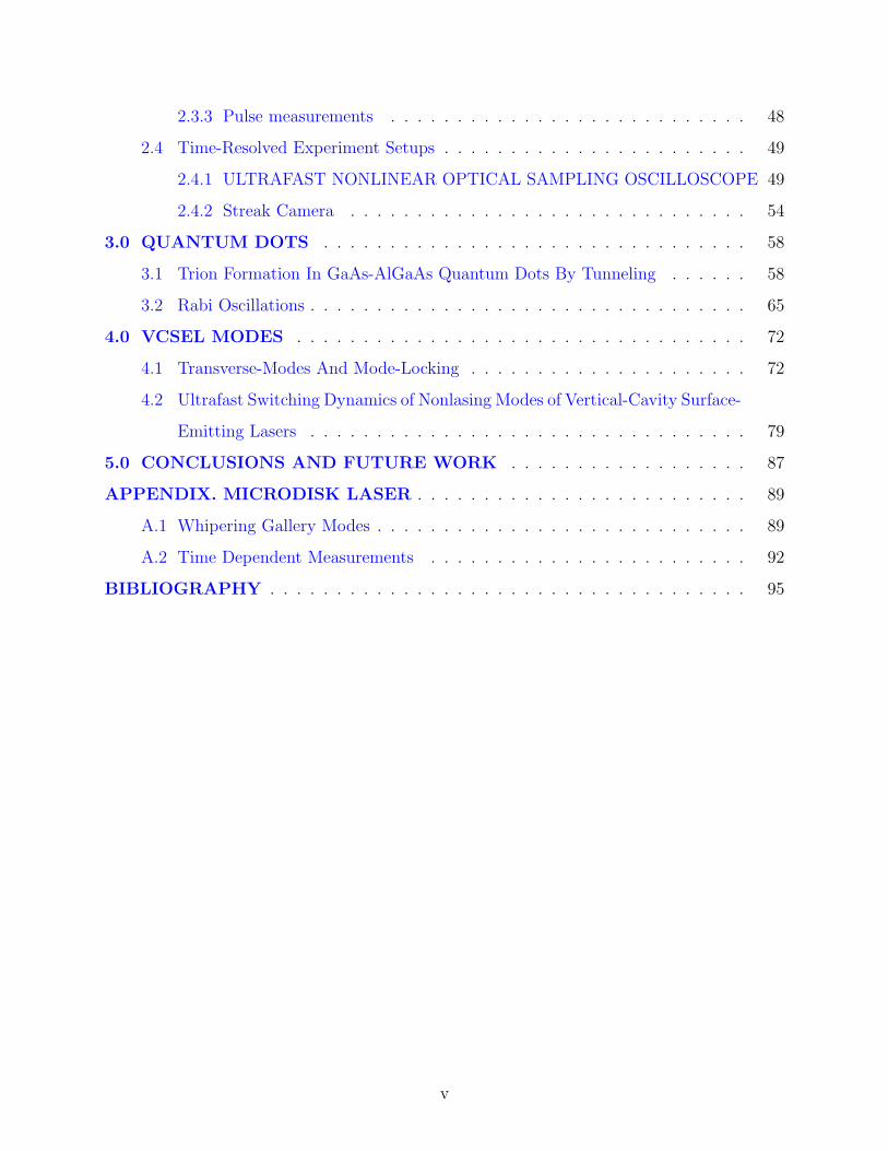
0.552
0.828
1.10
1.38
138
nW/div
uW
Figure 30: A typical spectrum measurement for a pulse with a FWHM on the order of 10 fs
(a typical pulse width measurement as shown in Fig. 40) from chirped mirror based cavity.
39

LensM1XtalM2
M3
M4
M5
M6
OC
θθ
Verdi -10
P1
P2
Slit
Figure 31: The schematic setup of tunable Ti:Sapphire oscillator with prism-pair design.
order to fine tune the dispersion, a pair of fused silica wedges is placed inside the cavity. The
wedge has an apex angle of 11 and the minimum thickness is about 1 mm. With this cavity,
we were able to generate a laser pulse with a bandwidth of 100 nm (FWHM), as shown in
Fig. 30 and a typical pulse width measurement is shown in Fig. 40.
A Kerr-lens mode-locked laser based on chirped mirrors can be very compact and easy to
align. It is an ideal choice if you just want to produce the shortest pulse possible. However,
in some applications, wavelength tuning is desired. In this application, a mode-locked laser
with a prism-pair is more versatile. Fig. 31 is a schematic setup for our laser cavity which
includes a pair of prisms. The prism pair is made of fused silica and has the Brewster cut for
minimizing the insertion loss when aligning the laser with minimum deflection angle. With
a prism pair, the dispersion can be fine tuned by moving the prisms in or out of the beam.
After the laser beam passes through the prism, it will be dispersed over a range of angles
depending on the individual wavelengths. A variable slit is placed at the end mirror side
after two prisms. By adjusting the width of the slit, we can control the spectral range of
the laser pulse. The desired center wavelength can be selected by moving the slit across the
beam.
One of the shortcomings of the Kerr-lens mode-locked lasers is that the pulsed emission
does not self-start [27]. However, a fast disturbance of the cavity usually starts the mode-
locking. Changing the cavity length rapidly is a commonly used method for starting the
40

mode-locking. For example, I just tapped one of the folding mirrors (M1 and M2) for
chirped-mirror-only cavity or quickly moved the prism in and out for a prism-based cavity
to initialize the pulsation. When the cavity is perfectly aligned, a high frequency vibration
of the optical table can start the mode-locking.
2.3 PULSE SHAPING
An ultrafast laser pulse is extremely narrow in the time domain and very broad in the
frequency domain. It has been proved to be an important super-speed laser source for
ultrafast optical impulses. However, a single laser pulse generated from the ultrafast laser
oscillator is a little “boring” sometimes. For many applications, the demand for more control
of laser pulses is critical, such as optical coherent control, high power laser amplification,
and optical frequency metrology etc. Pulse shaping is a very broad topic which exists in
any process to alter the pulse envelope, the phase of pulse or the power of pulse, and so
on. Actually, a Kerr-lens mode-locked laser cavity itself involves many pulse shaping process
such as self-amplitude modulation, self-phase modulation and dispersion control, etc.
2.3.1 Actively stabilized double pulse generation
One of the most common pulse shaping techniques is double pulse generation. Basically, a
single pulse splits into two pulses with a well defined time delay between them. For some
applications like optical coherent control of excitation states [42], the phase difference has
to be well defined. For many challenging experiments, the signal output is weak, so a long
time integration is needed. Therefore, the phase difference also needs to be maintained for
a long measurement time.
Fig. 32 shows the schematic setup for a computer controlled Mach-Zehnder interferom-
eter. The setup has two input ports, one is for a CW HeNe laser and the other is for the
Ti:Sapphire laser. The two beams have different linear polarization which are perpendicular
to each other, and a polarizing beamsplitter combines the two beams. At the output port,
41

Delay τ
τ
CW laser
Pulse laser
Polarizing
Beamsplitter
Nonpolarizing
Beamsplitter
RetroreflectorPolarization
Dual Si
Photodiode
Figure 32: The computer-based stabilized double-pulse generation.
another polarizing beamsplitter directs the CW laser to a quadrant phodiode and the laser
pulse to the experiment. Since the pulse laser has very short coherence length, the CW laser
is used to track the path length for two beams. At the quadrant diode side, the HeNe laser
produces an interference pattern which is magnified by a lens. We only use two detectors
of the quadrant diode for the detection of the interference pattern. For the best result, the
adjacent detectors have π/2 phase difference for the interference. To reduce the influence of
ambient light, a bandpass filter for the HeNe laser is attached to the quadrant photodiode.
The path difference is controlled by a speaker which is driven by a National Instruments
(NI) data acquisition (DAQ) card.
As shown in Fig. 33 (a), the x and y signals are from two adjacent detectors which
measure the interference of the CW HeNe lasers. The phase shift between two detectors is
about 0.56π or 0.28 cycle. If we plot x versus y as in Fig. 33 (b), we will get a complete
ellipse for a full interference period. Therefore, each point on the ellipse has a unique polar
angle which corresponds to a phase angle within a 2π phase cycle. Before every experiment,
42

0 0.5 1−4.5
−4
−3.5
−3
−2.5
−2
−1.5
Drive Voltage (volt)
Photod
iode
(volt)
xy
−4 −3 −2 −1−5
−4
−3
−2
−1
X voltage
Y v
olta
ge
(a) (b)
Figure 33: (a) The measured signal from the quadrant photodiode for X and Y detector.
(b) The measured ellipse based-on the X and Y signals, which works as the phase reference.
the unique ellipse has to be defined first, which then works as a phase reference. Usually, we
measured the full travel range of the speaker and used the Levenberg-Marquardt algorithm
[43] to find the reference ellipse. The red ellipse in Fig. 33 (b) is the fitted ellipse.
A standard ellipse equation is the following: x = a cos(θ)
y = b sin(θ)(2.15)
which is a simple ellipse centered at the origin, with a and b the half-axis lengths. Any other
ellipse can be transformed from Eq. (2.15) by rotation and translation operations:
x′
y′
= T + R ·
x
y
, (2.16)
where
T =
x0
y0
43

R =
cos(α) − sin(α)
sin(α) cos(α)
.
Basically, measured ellipses can be transformed back to a simple ellipse (Fig. 34). By scaling
the x and y coordinates with the half-axis lengths, a simple ellipse can be turned into a circle
which makes phase calculation even easier.
In practice, a computer-based proportional-integral-derivative (PID) loop stabilized the
path difference based on the feedback from the quadrant photodiode. Since all the calcula-
tions and controls are performed by a computer, the setup is easier and more flexible than
an analog PID device. A phase change bigger than 2π can also be tracked by implementing a
proper algorithm, and the accumulated phase change can be calculated as long as the speed
of speaker movement is slower than the PID loop rate. The Labview program we used has
up to 1 kHz rate. For higher speed and more determined time control, a real-time operating
system targeted PC is recommended. The PID loop rate is up to 1 MHz for the real-time
Labview program.
For more critical and stable experiments, a piezo actuator works better. However, the
travel range is only a few hundred micrometers. To realize long pulse delay, a stepper motor
can work together with a piezo actuator which can be easily programmed. This flexible
computer-based stabilized interferometer can maintain the path difference within 2% of the
HeNe laser wavelength (632 nm). It gives a 0.04 fs accuracy on the time delay between two
pulses.
2.3.2 Double-color double pulse generation
On the femtosecond scale, it is hard to directly modify the time profile in the time do-
main. The most effective way is to manipulate the amplitude and phase of pulse spectrum.
Dispersion control setup based on prism pairs or grating pairs are literally pulse shapers
which modify the phase information for different wavelength components. By controlling
the dispersion, we can compress or stretch the pulse’s time profile. This type of pulse shaper
was first demonstrated for picosecond pulses [44] and then extended to the application of
femtosecond pulses.
44
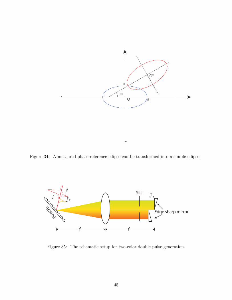
O"
O a
b
α
Figure 34: A measured phase-reference ellipse can be transformed into a simple ellipse.
Slit
Edge sharp mirror
τ
τ
f f
Grating
Figure 35: The schematic setup for two-color double pulse generation.
45
The pulse shaper consists of three main parts: the Fourier transform of the pulse, an
amplitude and phase mask, and the inverse Fourier transform. The Fourier transform of
the pulse is usually done by a prism or grating, which disperses the pulse in the frequency
domain,
E(w) = F[E(t)], (2.17)
and the function of amplitude and phase mask is,
M(w) = t(w)e−iϕ(w). (2.18)
After the mask, we get,
E ′(w) = M(w) · E(w). (2.19)
At last, by doing the inverse Fourier transform, we can get the shaped pulse,
E ′(t) = F−1[M(w)] ⊗ F−1[E(w)] = M(t) ⊗ E(t), (2.20)
where ⊗ stands for the convolution. Fig. 35 shows a typical spectral filtering pulse shaper.
The Ti:Sapphire laser pulse was collimated and aligned parallel to the optical table surface.
At the entrance of the setup, an 800 lines/mm grating was aligned with the input beam close
to the Littrow condition for the maximum diffraction efficiency where the diffracted beam
is collimated with the incident beam [45]. The spectrally dispersed pulses were collimated
by a lens which was one focal length away from the grating. After the lens, a high reflector
was placed on the focal plane of the lens. The laser beam was sent back to the entrance
and slightly off from the original beam height in order to pick up the modified pulses. The
alignment was a little tricky since we wanted to keep the distance between the grating, lens
and the reflector exactly at the focal length. If the distance between the lens and the grating
is not equal to the focal length, the pulse shaper will add chirp to the pulse which will stretch
or compress the output pulse. By looking at the output pulse width, we were able to find out
the correct distance between the lens and the grating. If the distance between the lens and
the reflector is not equal to the focal length, the output beam will diverge. Therefore, by
collimating the output beam, the distance between the lens and the reflector can be proper
46

750 755 760 765 770 775 7800
0.5
1
1.5
2x 10
−5
Wavelength (nm)
Inte
nsity (
a.u
.)
Figure 36: The shaped spectra.
adjusted. However, this aligning procedure needed several iterations since the two distances
are not independent.
In the Fig. 35 setup, two D-shaped edge mirrors are close together instead of a single
piece of reflector. An adjustable slit is also placed in front of the two edge mirrors. By
adjusting the slit width, the total bandwidth of the laser pulse can be tuned. At a result,
the pulse width will change accordingly. The distance of the two mirrors in the direction
perpendicular to the beam can also be changed, which gives the desired energy splitting for
output double pulses. The most intriguing feature of this setup is the ability to produce a
delayed double pulse by changing the distance between the two mirrors in the direction of
the beam.
Fig. 36 shows several measured shaped Ti:Sapphire laser spectra. The spectrum band-
width and the center wavelength can be easily tuned. The minimum bandwidth is down
to 0.3 nm (or 0.6 meV). Fig. 37 shows a time-resolved measurement for a two-color double
pulse. The energy splitting of the two pulses is 3.3 meV and the time delay is 12.6 ps.
47

Wavelength (nm)
Tim
e (
ps)
750 752 754 756 758
200
250
300
350
Figure 37: A typical two-color double-pulse measurement after the pulse shaper.
2.3.3 Pulse measurements
The femtosecond laser pulse is too short to be measured directly by photodetectors. The
only thing is comparable to the pulse is the pulse itself. Fig. 38 is a typical schematic setup,
called an autocorrelator, which uses the pulse itself to measure the pulse width. The setup is
based on a Mach-Zehnder interferometer which is symmetrical for the two beam path. One
of the retroreflectors is driven by a speaker (actually a voice coil). The detector is a GaP
photodiode which is only sensitive to 150 - 550 nm wavelength range. The Ti:Sapphire laser
pulse is around 700 -1000 nm. The detector also involves a nonlinear up-conversion process,
called two-photon absorption [46]. In order to measure pulse width and the dispersion, two
beams collinearly hit on the photodetector. A function generator drives the speaker at 3 Hz
and triggers an oscilloscope which acquires the signal from the photodetector. The speed
of the acquisition has to be much faster than the period of the speaker in order to resolve
interference fringes. The two-photon absorption signal is proportional to
D(τ) =
∫ ∞
−∞
∣∣[E(t) + E(t− τ)]2∣∣2 dt. (2.21)
48

Fig. 39 is an interferometric autocorrelation measurement for the laser pulse generated
from our prism-based Ti:Sapphire oscillator. The measured pulse width is about 353 fs and
the spectral bandwidth is 3 nm, which gives ∆τ∆v ≈ 0.4 as predicted in [30] for a Gaussian
shaped pulse.
Fig. 40 is an autocorrelation measurement for a laser pulse from our chirped-mirror-based
Ti:Sapphire oscillator. The setup used in this measurement was a little different from Fig.
38. Instead of a GaP photodiode, a light-emitting diode (LED) was used as the nonlinear
detector. The band gap of the LED gain material is higher than the photon energy from
a Ti:Sapphire oscillator, which means it needed a two-photon process to excite an electron
from the valence band to the conduction band. As seen in this figure, the measured pulse
was highly chirped. Due to the low number of sampling points, there was some distortion
on the measured signal which is supposed to be symmetric.
2.4 TIME-RESOLVED EXPERIMENT SETUPS
From previous sections, we have well-prepared Ti:Sapphire laser pulses as a tool to explore
ultrafast dynamics in several semiconductor systems. In this section, two kinds of time-
resolved detection apparatus are introduced: one is a pump-probe setup for femtosecond
dynamics measurements; the other is a streak camera system which features a 2 ps resolution
and photon counting sensitivity.
2.4.1 ULTRAFAST NONLINEAR OPTICAL SAMPLING OSCILLOSCOPE
The pump-probe setup is the most popular approach for time-resolved experiments. Usually,
a laser pulse, called the pump laser, first excites a system and induces some property change.
The change often varies with time. Another laser pulse, called the probe laser, has a certain
time delay τ with respect to the pump pulse to detect the property at different time τ .
Depending on the property we are interested in, different detecting methods are used such
as transmission, reflection and emission etc.
49

Delay τ
Nonpolarizing
Beamsplitter
Retroreflector
Speaker
Function
GeneratorOscilloscope
Trigger
GaP
Photodiode
Figure 38: The autocorrelator setup.
50
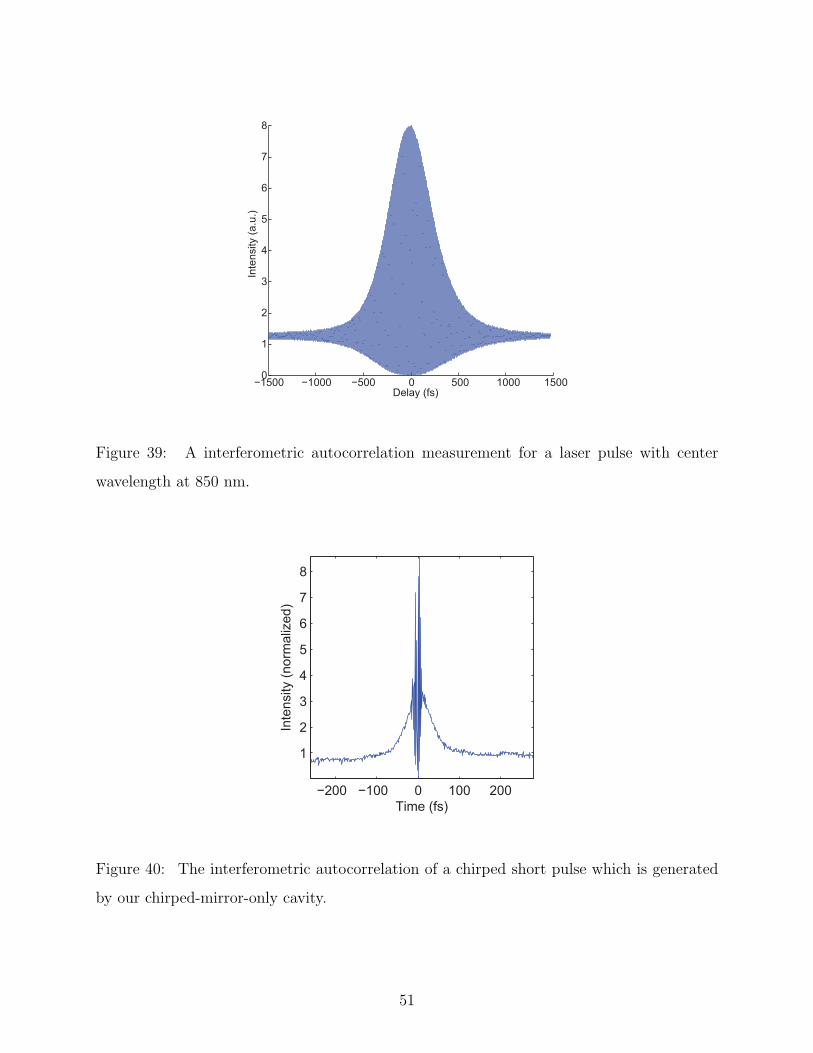
−1500 −1000 −500 0 500 1000 15000
1
2
3
4
5
6
7
8
Delay (fs)
Inte
nsity (
a.u
.)
Figure 39: A interferometric autocorrelation measurement for a laser pulse with center
wavelength at 850 nm.
−200 −100 0 100 200
1
2
3
4
5
6
7
8
Time (fs)
Inte
nsity (
no
rma
lize
d)
Figure 40: The interferometric autocorrelation of a chirped short pulse which is generated
by our chirped-mirror-only cavity.
51
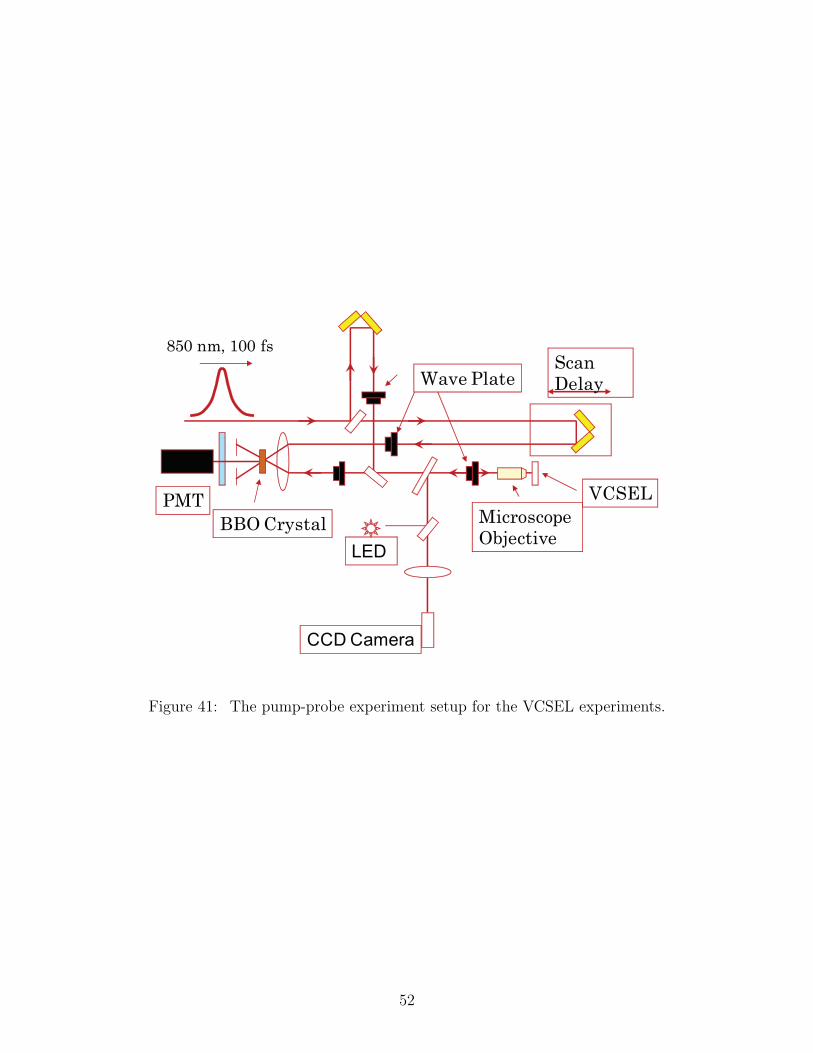
VCSEL
Scan
Delay
PMT
LED
CCD Camera
BBO Crystal Microscope
Objective
Wave Plate
850 nm, 100 fs
Figure 41: The pump-probe experiment setup for the VCSEL experiments.
52

Fig. 41 shows the pump-probe setup for resonant injection and probing ultrafast dynam-
ics from a VCSEL. The injection laser pulse is from our home-built tunable Ti:Sapphire laser.
The center wavelength of the laser pulse was tuned resonant to the emission wavelength of
the VCSEL. The bandwidth of the injection laser pulse is usually around 5 nm, which covers
the whole emission range of the VCSEL. Since the emission window of the VCSEL is on the
order of tens of microns, a confocal microscope was built to monitor the injection location
on the surface of the VCSEL wafer. Fig. 42 shows a single-mode VCSEL device image taken
with a 40X microscope objective.
The delay scan was driven by a 100 mm travel stepper motor stage with 1 µm resolution.
The signal was detected by a photomultiplier tube (PMT) with a preamplifier and collected
with a National Instruments multi-function data acquisition card. The stage was set up in a
way that sent out the trigger signal to the DAQ card and synchronized the data acquisition
with the delay scan.
Many single-mode VCSELs have a preferred linear polarization due to the strain built
in at the manufacturing stage. In order to study modes with different polarization, two
half-waveplates and two quarter-waveplates were used to control the injected laser pulse
polarization and the detection of the VCSEL emission polarization.
At the detection stage, an optical up-conversion technique is implemented. The key
component is a nonlinear crystal, which is a β-BaB2O4 (BBO) crystal in our case. The
emission from the VCSEL is up-converted by second harmonic generation. The probe pulse
works as a gating signal. The up-converted signal only occurs when both probe pulse and
the light emission from the VCSEL interact with the BBO crystal at the same time.
The second harmonic generation is related to the nonlinear response for electric field.
The polarization density can be expressed as [46]:
P = χε0E + 2χ(2)E2 + ...
where the first term is the linear response and the higher order term is related to nonlinear
response. The second order term represents the process of two photons forming a single
higher energy photon, which has to be satisfied with the energy conservation,
~wprobe + ~wV CSEL = ~wsignal
53

and the momentum conservation,
k(wprobe) + k(wV CSEL) = k(wsignal).
These two requirements are known as the phase-matching condition. Since all the mate-
rials have dispersion, the phase-matching condition can not be satisfied automatically. In the
case of a crystal, the birefringence makes the phase-matching possible in a certain direction.
For the single-axis crystal BBO, there are two kinds of phase-matching condition, depend-
ing on the polarization of input signal: one is that the probe beam and VCSEL emission
have same polarization, known as type-I phase-matching; the other is that the probe beam
and VCSEL emission are cross-polarized, called type-II phase-matching [47]. In the VCSEL
experiments. we used type-I phase-matching due to the higher up-conversion efficiency.
2.4.2 Streak Camera
Although the ultrafast optical up-conversion technique has time resolution limited by the
pulse width, the alignment is tricky and the detection efficiency and sensitivity are low. If
the dynamics of the studied system are on the order of picosecond, a streak camera system
will suit the application better.
Fig. 43 shows a schematic setup for a commercial Hamamatsu streak camera system. An
optical signal first hits on a fast-response photocathode which converts photons to electrons.
The electrons are accelerated to fly through the streak tube which is in a high vacuum state.
As electrons pass through the streak tube, a vertical electrical field disperses the electrons
along the vertical direction. In the time order of the photons hitting on the cathode, electrons
will hit on different positions of a phosphor screen. At the phosphor screen, electrons are
converted to photons and then detected by a CCD camera which converts photons back to
electrons again.
Compared to the optical sampling method, a streak camera system is much more sensitive
over 300 nm to 850 nm range. The setup is much easier and there is no need for a time
delay scan, which increases the measurement stability and speed. In most cases, the optical
sampling method only samples one point at a time. Instead, a streak camera system can
54

Figure 42: A typical image of a single-mode VCSEL device.
Figure 43: The operation principle of streak camera. (The picture is from Hamamatsu.)
55

SpectrographStreak camera
Microscope
cryostat
Trigger signal
CCD camera
Microscope
objective
White
light
Waveplate
Polarizer
Figure 44: The streak camera experiment setup for quantum dots experiment.
56

time-resolve one line at a time. If a spectrometer is connected to the streak camera, multi-
channel time-resolved spectra can be done pretty quickly. The optical sampling method only
measures the signal average over millions of pump pulses. In addition, streak cameras can do
single-shot measurements, which are useful for studying correlations between different pump
laser pulses.
Fig. 44 is the schematic setup for the streak camera system which was used to mea-
sure our quantum dots emission dynamics. Before being sent to the sample stage, the
Ti:Saphhaire laser pulse passed through a pulse shaper which can tune the laser resonant to
the quantum dots excitation state and limit the bandwidth of the laser pulse.
57
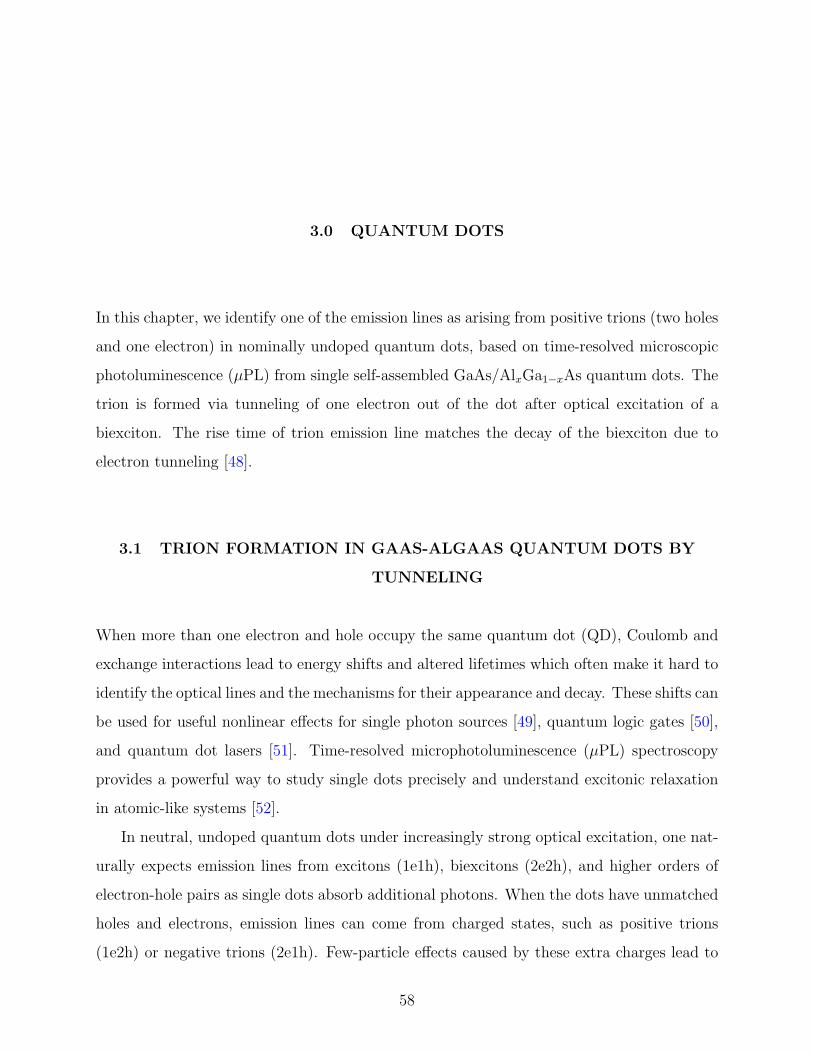
3.0 QUANTUM DOTS
In this chapter, we identify one of the emission lines as arising from positive trions (two holes
and one electron) in nominally undoped quantum dots, based on time-resolved microscopic
photoluminescence (µPL) from single self-assembled GaAs/AlxGa1−xAs quantum dots. The
trion is formed via tunneling of one electron out of the dot after optical excitation of a
biexciton. The rise time of trion emission line matches the decay of the biexciton due to
electron tunneling [48].
3.1 TRION FORMATION IN GAAS-ALGAAS QUANTUM DOTS BY
TUNNELING
When more than one electron and hole occupy the same quantum dot (QD), Coulomb and
exchange interactions lead to energy shifts and altered lifetimes which often make it hard to
identify the optical lines and the mechanisms for their appearance and decay. These shifts can
be used for useful nonlinear effects for single photon sources [49], quantum logic gates [50],
and quantum dot lasers [51]. Time-resolved microphotoluminescence (µPL) spectroscopy
provides a powerful way to study single dots precisely and understand excitonic relaxation
in atomic-like systems [52].
In neutral, undoped quantum dots under increasingly strong optical excitation, one nat-
urally expects emission lines from excitons (1e1h), biexcitons (2e2h), and higher orders of
electron-hole pairs as single dots absorb additional photons. When the dots have unmatched
holes and electrons, emission lines can come from charged states, such as positive trions
(1e2h) or negative trions (2e1h). Few-particle effects caused by these extra charges lead to
58

an energy splitting between neutral states and charged states [53]. While it is easy to see
how trions could arise in doped dots with excess charged carriers [54], for trions to appear
in undoped dots either extra free carriers must be captured from outside the dot, or photo-
excited carriers must escape the dot. In nominally undoped InAs [55] and CdSe [56] dots, the
appearance of trions has been attributed to capture of free carriers excited in the substrate
by photons with energy well above the band gap of the barrier material.
Here I present evidence that trions in a new type of undoped GaAs quantum dots [16]
can even appear for below-barrier excitation. The trions are formed when electrons escape
the dots by tunneling as shown by time-resolved studies in samples with different barrier
thicknesses. This interpretation explains why time integrated spectra [57] show a trion line
that is much more intense than the bi-exciton emission.
The structures studied here consist of hierarchically self-assembled GaAs/AlxGa1−xAs
QD’s grown by molecular beam epitaxy combined with in situ etching of GaAs-capped InAs
QDs [16]; the samples are very similar to those studied in Ref. [57], and the binding energy
of 2.9 meV for the trion determined in Ref. [57] is very close to the value of 3.0 meV which
we determine here. The QD size dispersion produces inhomogeneous broadening of about 10
meV for the ground state emission, which is less than that of “natural” QD’s occurring due
to thickness fluctuations of GaAs/AlGaAs quantum wells (QW). Since the dot material is
GaAs, the emission wavelength range is well matched to the multi-alkali photo cathode in our
streak camera system, which makes the ultra high speed and high sensitivity measurements
possible. Compared to self-assembled InAs QD’s, the QD’s studied here have an inverted
shape, and they are located under a thin GaAs QW (see Ref. [16]). The GaAs QD’s are
sandwiched between two AlxGa1−xAs layers. The bottom Al0.45Ga0.55As layer (thickness
D) inherits the nanohole structures from InAs quantum dots after etching. By varying the
barrier thickness D, different sizes of nanoholes on the top of the Al0.45Ga0.55As layer can be
realized. For the samples investigated here, with D = 7 and D = 10 nm, the holes have a
depth of 4.1 and 3.2 nm, respectively, and a lateral width of 50 nm (see Ref. [16]).
The QD samples were mounted inside a continuous flow microscope cryostat, and all of
the experiments were performed at a temperature of 10 K. A tunable mode-locked ultrafast
Ti:Sapphire oscillator with a repetition rate of 76 MHz was used as pump laser. The laser
59

pulse spectral width (FWHM) was 3 nm. The measurement stage of the experimental
setup consisted of a confocal microscope and a spectrograph connected to a Hamamatsu
streak camera system with a time resolution down to 3 ps. Using a high numerical aperture
(NA = 0.8) microscope objective, we were able to focus the laser beam down to 1 µm. In this
experiment, we studied two kinds of samples with different QD surface densities: two high-
density quantum dot (HDQD) samples with 40 dots per µm2, and one low-density quantum
dot (LDQD) sample with an average of 0.5 dots per µm2.
Figure 45 shows the time-resolved µPL of HDQD samples with different barrier thick-
nesses D for near-resonant excitation with a photon energy of 1.699 eV, which is above the
dot luminescence energy and below the energy of the QW’s (1.777 eV) next to the dots. The
fundamental emission energy is higher for the sample with the thicker barrier, which indi-
cates stronger confinement [16]. The linewidth of the emission peak is 10 meV. We extracted
the decay dynamics for each emission maximum of the two QD samples, shown in Figure
45(c), by integrating over a 10 meV spectrum width. Both samples have similar rise times
of ∼ 38 ps but different decay times, 318 ± 4 ps for the D = 10 nm QD sample and 254 ± 4
ps for the D = 7 nm sample.
The total decay rate, τ−1tot , of excitons is the sum of radiative decay rate, τ−1
rad, and the
rate for electron (or hole) tunneling out of the dot, τ−1tun, i.e.,
1
τtot=
1
τrad+
1
τtun(3.1)
The stronger confinement of the dots with thicker barrier should imply larger oscillator
strength, which means shorter decay time [58], but here the sample with thicker barrier
has longer lifetime. Therefore, we attribute the significant decay time difference for the
two samples to tunneling through the barrier between the QD’s and the QW’s. Since the
effective mass of heavy holes is much larger than that of electrons, the rate of heavy hole
tunneling is much lower than that of electrons (still shorter than laser pulse interval). Hence,
electron tunneling should contribute most to the initial stage of tunneling decay. Exponential
dependence of tunneling time with barrier thickness has been shown for AlAs/GaAs double
quantum well samples [59] and vertically aligned double quantum dots [60].
60

Energy (eV)
Tim
e (
ps)
(a) D=10 nm
1.62 1.64 1.66 1.68
0
500
1000
Energy (eV)
(b) D=7 nm
1.59 1.61 1.63 1.650
5
10
15
0 200 400 600 800 1000 120010
1
102
103
7 nm
10 nm
Time (ps)
PL
(co
un
ts)
(c)
xx x+(d)
Figure 45: Time-resolve µPL measurements of high density QD samples with different
barrier thicknesses of D = (a) 10 nm, and (b) 7 nm. (c) The decay dynamics for both
samples, where the solid white lines are exponential fits. The pump power is 200 µW. (d)
The process of a biexciton (XX) turning into a positive trion (X+) by electron tunneling.
61

Tim
e (
ps)
Energy (eV)
X
(a)
1.61 1.615
0
100
200
300
400
500
600
Energy (eV)
XX+
(b)
1.61 1.615
Energy (eV)
XX+XX
(c)
1.61 1.615
0
0.2
0.4
0.6
0.8
1
0 0.5 110
1
102
Time (ns)
Inte
nsity (
co
un
ts)
X
(d)
0 0.5 1
Time (ns)
X+
(f)
0 0.5 1
Time (ns)
XX
(e)
Figure 46: Time-resolved µPL for single QD’s. (a), (b) and (c) are streak camera images
for pump powers of 40µW , 80µW and 160µW , respectively (The dark line at time zero
is scattered light. The intensity is normalized in each image); (d), (e) and (f) are decay
dynamics of exciton (X), biexciton (XX) and positive trion (X+), respectively, where the
black dots are experimental data and the solid white curves are simulations from the rate
equations (3.4).
62

Since the lateral sizes of our QD’s are large compared to their heights, we can approximate
tunneling as a one-dimensional process. By the solving the one-dimensional Schrodinger
equation, the transmission coefficient T is
T = (1 +(k2 + β2)2
4k2β2sinh2 βD)−1 βD≫1
≈ ∆ exp(−2βD), (3.2)
where k =√
2m1,eE/~, β =√
2m2,e(V0 − E)/~, ∆ = 16k2β2/(k2 + β2)2, and m1,e and
m2,e are the effective electron masses of GaAs and GaAs/Al0.45Ga0.55As, respectively; V0 is
the conduction band offset for GaAs/Al0.45Ga0.55As heterostructures, and E is the electron
confinement energy inside the quantum dots. Under the WKB approximation, the tunneling
time varies exponentially with the barrier thickness D according to [61]
τtun ≈ 2m1,ea
~kT≈ 2m1,ea
~k∆exp(2βD), (3.3)
where a is the height of the QDs. Therefore, the QD sample with D = 10 nm has a tunneling
time of the order of several tens of ns. We can approximately treat the total decay time as
mainly radiative decay time for this thicker-barrier sample. From Eq. (3.1) and the fitted
decay time for the thinner-barrier sample, we obtain an electron tunneling time of 1.262 ns.
By comparison, Equation (3.3) gives us an electron tunneling time of 1.1 ns for a barrier
thickness of D = 7 nm, which is in fairly good agreement with the value extracted from the
experimental data.
Tunneling of an electron from a biexciton should produce a positive trion that can be
resolved in single dot experiments due to the absence of inhomogeneous broadening and the
resulting emission line width. With the LDQD samples, we were able to excite single QD’s
without a mask mesa pattern or etching the samples, as was necessary in Ref. [55]. The
LDQD sample we used here had a barrier thickness of D = 7 nm. As Figure 46 (a)-(c)
shows, the single QD spectra have sharp emission lines with 240 µeV line width, which is
limited by the system resolution. At very low pump power, the single QD’s only show a
fundamental excitonic line (X) at 1.615 eV. With increasing pump power, we can clearly see
two more emission lines at 1.612 eV and 1.609 eV. As discussed in the following, these lines
correspond to the positive trion (X+) and the biexciton (XX), respectively.
63

From Figure 46 (c), the X+ line shows a clearly delayed emission with respect to the XX
and X lines. In principle, multi-excitonic complexes could also arise from extra carriers ex-
cited in the material surrounding the dots, followed by migration into the dots [62], since the
background doping is nominally around 1015 cm−3 in GaAs-based structures [63]. Creation
of these complexes due to in-tunneling of carriers would imply a much longer rise time for
the biexciton emission, however, as carriers diffuse to the dots. Since we excited below the
barrier, we do not expect this to be a strong process, although a small amount due to two-
photon absorption is possible. The long rise time of the trion line compared to the rise time
of the biexciton line gives a clue to the positive trion formation process: a biexciton loses an
electron through tunneling, leaving behind a positive trion. At the same time, a biexciton
can also decay by photon emission, leaving behind an exciton. Keeping these points in mind,
we can write a simple set of rate equations to explain the multi-excitonic decay dynamics:
dNxx
dt= − Nxx
τxx,rad− Nxx
τxx,tun
dNx
dt= − Nx
τx,rad− Nx
τx,tun+
Nxx
τxx,rad
dNt
dt= − Nt
τt,rad− Nt
τt,tun+
Nxx
τxx,tun
(3.4)
where Nx(t), Nxx(t) and Nt(t) are the ensemble average at a single point in time of the
number of excitons, biexcitons and trions, respectively, for a single dot excited many times
by the repeated laser pulse. The lifetimes τx,rad, τxx,rad and τt,rad are the radiative decay
times for excitons, biexcitons and trions, respectively, and τx,tun, τxx,tun and τt,tun are the
electron out-tunneling decay times for the excitons, biexcitons and trions.
Eq. (3.4) implies that the biexciton population has single exponential decay. Since the
density of biexcitons is small compared to that of excitons, the contribution to the exciton
population due to biexcitons radiatively decaying into excitons is negligible. Therefore,
the exciton line also has approximately single exponential decay. Since the biexciton and
exciton data can each be fit by single parameter fits, we have a simple two-parameter fit
for the trion decay. At high pump power, because we excite the dots with photon energy
64

above the lowest confined states (but still well below the barrier height), there is an initial
population of excitons and biexcitons in excited states. This means that the population is
not entirely in the lowest exciton and biexciton states until after a thermalization time of
around 150 ps. Therefore, we only fit the intensity decay data after t = 156 ps.
As shown in Figure 46 (d)-(e), we can obtain good fits to all three time-resolved intensity
plots, for τx,tot ≈ 232 ps, τxx,rad ≈ 446 ps, τt,rad ≈ 289 ps, τxx,tun ≈ 271 ps and τt,tun ≈ 572
ps. The electron out-tunneling time for the trion, τxx,tun, is almost twice of τxx,tun consistent
with the fact that the biexciton has two electrons, which doubles the total tunneling rate.
The consistency of these fits confirms the identification of the line we have identified
as coming from the trion. Although in some cases the positive trion line can lie higher in
energy than that of the exciton [64], it can have lower energy than the exciton for relatively
large QD’s [63], as seen here. The energy shift is also confirmed by polarization dependence
measurements [57].
In conclusion, time-resolved µPL measurements of unstrained self-assembled
GaAs/AlxGa1−xAs QDs with high spectral resolution are consistent with the picture that
at high excitation density, biexcitons are formed in the dots, followed by electron tunneling
out of the QDs, leaving behind a positively charged trion. This indicates that for the thin
barrier samples, the tunneling effect is an important source for the excitonic decay.
3.2 RABI OSCILLATIONS
The broadband femtosecond laser source was initially used to do time-resolved photolumi-
nescence experiment. On the other hand, the energy splitting between exciton and biexciton
energy level is on the order of a few meV at the temperature of 10 K. Therefore, it is impos-
sible to selectively excite different transitions. As discussed in Section 2.3.2, the constructed
femtosecond laser pulse shaper is able to trim down the pulse bandwidth to 0.6 meV. A
well-defined two-color double pulse can address the excitonic and biexcitonic transitions for
the control of condition quantum gate operation.
Fig. 47 is a two-dimensional photoluminescence excitation (PLE) measurement on a
65

Pump Wavelength (nm)
Wa
ve
len
gth
(n
m)
PLE
751 751.5 752 752.5 753 753.5 754 754.5
765
766
767
768
769
770
771
772
773
774
775 0
50
100
150
Figure 47: A two-dimensional photoluminescence excitation (PLE) measurement on a single
quantum dots. The horizontal axis shows excitation wavelength, whereas the vertical axis is
the emission spectra.
66

single quantum dot. The pump beam was focused down to a sub-micron spot size in order
to excite as few dots as possible on a low-density quantum dots sample. To isolate a single
dot, the pump laser with a bandwidth of 0.6 meV was tuned resonant to an excited state
for a single quantum dots. The horizontal axis is the excitation wavelength and the vertical
axis is the emission wavelength. At 768.2 nm emission wavelength, there is a sharp line
which is much stronger than the line around 769 nm emission wavelength. That is because
the excitation laser only has 0.3 nm bandwidth which mainly excites single excitons. At
the same time, the pump power is sufficiently low so that it does not saturate the excitonic
transition.
With the sharp resonance, I can also select the quantum dots I want to excite and
differentiate different quantum dots by their resonant frequency. Fig. 48 shows the photolu-
minescence measurement from three quantum dots by scanning the excitation wavelength.
Dot 1 and dot 2 show pretty sharp resonance which means the lower-order excited states have
pretty narrow linewidth. However, Dot 3 shows pretty constant PL at 769 nm which might
be caused by broad high-order, excited-states resonance. For each dot, the fundamental
excitonic line is much stronger than the trion line on the lower energy side.
Rabi oscillation is a unique signature of light-matter quantum interaction for a two-level
system which is analogous to a classical harmonic oscillator. At resonant excitation, the PL
of quantum dots exhibit a sinusoidal oscillation versus the excitation pump power, which is
proportional to the field integral [65],
θ(t) =
∫ t
−∞pE(t′)/~dt′, (3.5)
where p is the transition dipole matrix element and E is the electric field of the excitation
pulse.
Fig. 49 (a) shows the luminescence intensity versus the square root of the power for the
exciton line at 762.8 nm. The emission saturates for increasing power and shows damped os-
cillatory behavior. This power dependence indicates Rabi oscillations between the unexcited
state and the E2 single exciton state, as shown in the Fig. 49 (b). The excited excitons relax
to E0 where they produce the observed excitons. The diagram does not take into account
67

750 755 760 765 770 775 780 785 7900
100
200
300
400
500
600
700
800
900
751.6 nm
751.2 nm
750.8 nm
750.4 nm
750 nm
749.6 nm
Wavelength(nm)
Inte
nsity (
co
un
ts)
Original Spectra
Dot 1 Dot 2 Dot 3
Figure 48: A photoluminescence excitation measurement on a single quantum dots.
68

0 10 20 30500
1000
1500
2000
Pump Power (µW1/2
)
762.8097 nm
Inte
nsity (
a.u
)
Unexcited
E0
E1
E2
Detection
Resonant
(a) (b)
Figure 49: A rabi oscillation measurement on a single quantum dots.
the level fine structure or multiple exciton behavior. The relaxation process disrupts the
Rabi oscillations and leads to the damping of the amplitude.
A simple approach for a resonant interaction system is called the rotating wave approx-
imation, which is commonly used in the magnetic pseudospin problem [12]. In the optical
resonance case, the pseudospin is actually the Bloch vector which stands for the state of a
two-level system. In the rotating wave approximation, the Bloch vector,
ρ = (u, v, w) (3.6)
works as a solid body which will precess around a certain axis under the external “torque”,
the driving electric field. The motion of the Bloch vector can be interpreted by
dρ
dt= Ω × ρ
and
Ω =
−pE~
0
∆
, (3.7)
69

Figure 50: Numerical simulation of Rabi oscillation vs. pump laser frequency detuning.
70

where ∆ the frequency detuning from the resonant frequency. In matrix expression, the
optical Bloch equation is
d
dt
u
v
w
=
0 −∆ 0
∆ 0 pE/~
0 −pE/~ 0
u
v
w
(3.8)
Fig. 50 shows a calculation for the Rabi oscillation versus detuning at the presence of a
2 ps optical pulse excitation. For direct Rabi oscillation observation, the resonant excitation
to the E0 transition should be used. However, it is impossible to do so in the current streak
camera setup. For such experiments, a pump-probe setup needs to be added.
71

4.0 VCSEL MODES
There are two sections in this chapter. For the first section, we have investigated the lasing
modes of oxide-confined vertical-cavity surface emitting lasers (VCSEL). The individual
Laguerre-Gassian modes have been spectrally and spatially resolved with scanning confocal
microscope with time resolution of 4 ps. Subject to the injection of ultrafast laser pulses, the
VCSEL showed irregular pulsed emission which indicates the potential for transverse mode-
locking of the VCSEL [66]. In the second section, single-mode vertical-cavity surface-emitting
lasers (VCSEL) have been investigated with ultrafast optical modulation. After injection
of a subpicosecond laser pulse into the VCSEL cavity, nonlasing modes were excited and
produced optical beating in the emission of the VCSEL. By measuring the decay time of
nonlasing modes, we find the round-trip gain of nonlasing modes and the stability of the
single-mode operation of the VCSELs. At high power, the VCSEL also shows polarization
switching effects [67].
4.1 TRANSVERSE-MODES AND MODE-LOCKING
With the mode-locking method, semiconductor lasers can produce picosecond laser pulses at
high repetition rates. Besides the pulse generation, mode-locked semiconductor lasers have
been used for all-optical clock generation [68] and producing frequency combs for optical
metrology [69].
There are two kinds of mode-locking method: active configuration with external modu-
lation and passive configuration with a fast saturable absorber. Since mode-locking requires
equidistant mode spacing, the longitudinal modes well-defined by the cavity length are the
72

Figure 51: The schematics of experiment setup.
natural choice for the mode-locking. These have been demonstrated with edge-emitting de-
vices in monolithic and external-cavity configurations [70], as well as in vertical external
cavity surface emitting lasers(VECSEL) [71]. On the other hand, a VCSEL only has one ac-
cessible longitudinal mode due to the short cavity length, which is not possible to be locked.
But most VCSELs have complicated transverse modes, and [72] showed these mode-locked
lateral modes generated picosecond pulse trains with ion-implanted VCSELs. In principle,
these transverse modes can be equally spaced in frequency, allowing mode-locking. This type
of mode-locked laser pulse will circulate around the VCSEL’s surface. Compared with proton
implanted VCSELs, oxide-confined VCSELs have better index guiding and more symmetric
mode profile which should work better for transverse mode-locking.
Here, I describe the spatial-spectrally resolved transverse modes of oxide-confined VC-
SELs. The transverse modes dynamics following ultrafast laser pulse injection were also
explored. The competition of the transverse modes led to an irregular pulsed emission.
The multitransverse mode VCSELs we studied are commercially available oxide-confined
VCSELs. This type of VCSEL uses lateral wet oxidation of an AlAs layer to produce the
aperture necessary for current and optical guiding. The threshold current of our samples is
73

847 848 849 850 851
−80
−70
−60
−50
Wavelength (nm)
Em
issio
n (
dB
m)
Figure 52: A typical emission spectrum of a multitransverse mode VCSEL at a bias current
of 8 mA.
Figure 53: The spatial-spectrally resolved VCSEL’s transverse mode at bias current 8.0
mA.
74
1.6 mA and the emission aperture is 15 µm. The typical emission wavelength is around 852
nm. A 100x microscope objective and a lens with 150 mm focal length were used in a scanning
confocal microscope configuration, as shown in Fig. 51, to give us 65x magnification. With
an optical spectrum analyzer (OSA) as a detector, we studied the spatial distribution of
each transverse mode. A mode-locked femtosecond laser was tuned to a wavelength center
at 850 nm with 3 nm bandwidth which covers the whole wavelength range of the VCSEL’s
emission. After the optical injection, the spatio-temporal resolved emission dynamics were
measured by an imaging spectrometer and streak camera system.
As seen in Figure 52, this type of broad-area VCSEL usually shows multimode behavior
in a spectrum measurement. Experimentally observed spatial images for each transverse
mode are shown in Figure 53. In this spatial-resolved mode experiment, the VCSEL was
biased at 8 mA, without any optical injection. We can clearly resolve the spatial distribution
of each mode. Similar mode images have been shown by [73] with an etalon filter and an
imaging spectrometer. Pereira et al. [74] excited unprocessed VCSEL layers with a ring-
shaped optical beam to demonstrate lasing in daisy-shaped Laguerre-Gaussian (LG) modes.
Commercial oxide-confined VCSELs usually have top ring-shaped contacts which inject
carriers annularly. The profile of the complex refractive index determines the transverse mode
distribution. A comprehensive model [75] has been applied to proton-implanted VCSELs
which shows parabolical carrier concentration and temperature distribution near the center
active region of VCSELs. From the temperature dependence of the index of refraction [76],
we can get a temperature-induced parabolic profile of the index of refraction. The transverse
modes have well-known analytical solutions for this kind of so-called square law medium,
i.e., nr = n0 − 12n0
a2r2, where nr is the effective refraction index, n0 and a are constants[74].
The normalized mode intensity is given by [74]:
I(r, θ) =4
l!
1
w2(2r2
w2)lexp(−2r2/w2)
1
πcos2(lθ), (4.1)
where r and u are the radial and azimuthal coordinate, respectively. The waist parameter is
given by w−2 = k0a/2, and the frequency separation between consecutive high-order modes
with increasing l is constant at δv = ac/(2πn20), where c is the speed of the light.
75

a)
b)
LG00
LG03 LG04 LG05
LG01 LG02
Figure 54: a) The first six order of LG modes calculated from equation (4.1). b) Moving
spots generated by interference of the six lowest order LG daisy modes. The diagram shows
the calculated intensity versus position on a mode-locked VCSEL for constant time steps
between t = 0 and 1/(2δv) , the time it takes the spots to move half the circle.
76

Figure 54(a) shows the profile of a few LG modes calculated by Equation (4.1). Since the
LG modes have constant frequency difference, locking these modes so that they are exactly
in phase at times t = n/(δv) (where n is integer), produces two bright spots going around
a circle in opposite directions with frequency δv . Figure 54(b) shows the motion of the
spots for half a period, calculated under the assumption that the fields of the modes can
be superposed linearly and that nonlinear effects are weak. The diagram shows that the
emission spot evolves during the motion due to the discrete nature of the modes.
Unfortunately, as shown in Figure 55(a), the mode spacing of our laser is not constant.
Presumably, small deviations from a perfectly parabolic index profile (seen in the non-pefect
circular symmetry in the mode shapes of Fig. 53) lead to the deviation from even spacing.
The non-perfect circular symmetry also breaks down the degeneracies of the LG modes with
π/2 phase shift, such as LG01 and LG01∗ at 850.25 and 850.20 nm.
Although we do not expect periodic mode-locking when the modes are not evenly spaced,
we can still see pulsed behavior. Based on the mode images and frequencies from Fig. 53,
we calculate the time dependence of the emission pattern of the measured VCSEL by simple
superposition. The theoretical time-resolved emission from the center strip of the VCSEL
is shown in Fig. 55(b). There are two types of mode-beating patterns: one is the mode
interference between different order of LG modes such as LG00, LG01 and LG02 etc. The
beating frequency is on the order of 100 GHz. On the top of the fast mode beating, there
is slowly varying modulation which is on the order of 20 GHz. This slow modulation is
caused by the splitting between two degenerate modes such as LG01 and LG01∗ . For proper
mode-locking operation, the slow modulation should be avoid.
Under normal circumstances, a VCSEL will not start mode-locking automatically. It
usually requires some mechanism to synchronize the phase of different transverse modes
first. In the experiments, we used ultrafast pulse injection to give all the lasing modes a well-
defined starting phase, as in the work of [72]. Figure 56 shows the time-resolved emission at
two lasing mode maxima after an injected 150 fs laser pulse. The injection laser was focused
into one of the lasing maxima located at the side of the emission aperture. The VCSEL
started to produce pulsed emission after the laser excitation. The time intervals between
pulses are not constant, and the mode-locked pulse can not be sustained, as expected for
77

Time (ps)
Positon (
a.u
.)
100 200 300
10
20
30
0 5 10 150
5
10
15x 10
10
v (
Hz)
(a)
(b)
Figure 55: (a) Experimental frequency difference between adjacent LG modes at bias current
8 mA for the modes shown in Fig. 53. (b) Theoretically calculated time-resolved emission
from the center strip of the VCSEL with modes shown in Fig. 53.
Figure 56: The streak camera image of a VCSEL’s emission (the slice of the VCSEL as
shown on the left) after a laser pulse injection at one of the VCSEL emission mode maxima.
This VCSEL has broader active region than the VCSEL used in Fig. 53 and 55.
78

non-equidistant mode spacing.
We have spatial-spectrally resolved the emission from commercial oxide-confined VC-
SELs. Our studies show that LG transverse modes can be used to mode-lock the lasers.
Subject to the synchronization of ultrafast laser injection, the laser shows irregular pulsation
effects. For excitation of evenly spaced LG modes in energy, we need a well-defined parabolic
index of refraction profile. Here, the temperature-indexed parabolic index of refraction pro-
file has asymmetrical shape which leads to non-periodic pulsing. In the future, we propose to
introduce a built-in parabolic index of refraction profile by tuning the material index during
the growth process.
4.2 ULTRAFAST SWITCHING DYNAMICS OF NONLASING MODES OF
VERTICAL-CAVITY SURFACE-EMITTING LASERS
Vertical-cavity surface-emitting lasers (VCSELs) have been widely used in optical communi-
cation and laser spectroscopy. A VCSEL’s cavity, which is typically one and a half wavelength
long, will support only one longitudinal mode and a few traverse modes. By lateral optical
confinement, the number of lasing transverse modes can be controlled. One of the methods
is to use oxidized AlGaAs layers as an aperture which provides excellent optical guiding and
current injection confinement. To achieve single-mode operation of VCSELs, the oxide aper-
ture usually is about 3 µm [77]. Due to the directional asymmetry, e.g. crystal structure,
strain, etc., the emission of a single-mode VCSEL usually has one preferred polarization [77].
However, under high frequency or high current modulation, single-mode VCSELs can have
multimode emissions which can contaminate the quality of the single-mode emission.
In this section we demonstrate a new method to study the lifetime and round-trip gain of
nonlasing modes of single-mode VCSELs and investigate the GHz/THz behavior of VCSELs
for ultrafast all-optical switching. Many time-resolved measurements of VCSELs have used
off-resonant injection to introduce an ultrafast current pulse [78, 77, 79]. Here, femtosecond
(fs) laser pulses with center wavelength resonant to the VCSEL’s emission wavelength were
injected into a sample laser to perturb the intra-cavity light field directly. After the optical
79

Microscope
ObjectivePMTBBO
OSA
VC
SE
L
Laser
Pulse
Delay Line
Fiber
HWP
Figure 57: The schematics of the optical up-conversion pump-probe experiment setup.
injection, the subsequent emission dynamics of the lasing and nonlasing modes of the VCSELs
were measured by a pump-probe optical up-conversion technique [72, 79].
The single-mode VCSELs we investigated are commercial oxide-confined lasers. The
lasing threshold is 1.0 mA and the center emission wavelength is around 852 nm. The
oxide aperture tightly restricts the optical emission window to suppress high-order transverse
modes. Above the threshold, the VCSEL’s emission is linearly polarized and shows redshift
with increasing injection current. To investigate the nonlasing mode behavior, we used
cross-polarized injection geometry (e.g. the VCSEL’s emission polarization is perpendicular
to that of the injected laser pulses). The laser pulses were produced by a mode-locked
Ti:Sapphire oscillator pumped by a solid state Nd:YVO4 laser. The center wavelength of
the fs laser pulses was tuned to 852 nm, with 200 fs duration, which covers all the emission
wavelength range of our single-mode VCSELs.
Figure 57 shows the schematic experimental setup. The injection laser pulse polarization
was controlled by a half waveplate. In front of the VCSEL, there is another half waveplate
to rotate the polarization of VCSEL’s emission. The reflected pump laser pulses, VCSEL
emission and probe laser pulses were focused onto a nonlinear β-bariumborate(BBO) crystal.
Type-I phase matching was used in the experiment to have better quantum efficiency for
weak continuous wave (CW) emission from the VCSEL. A slit can block most of the strong
80

Ti:Sapphire laser pulses by taking advantage of the cross-correlation setup. A BG40 color
filter further suppresses non-upconverted signals. Up-converted signals were detected by a
photomultiplier tube (PMT) which is only sensitive to 300 to 650 nm wavelength. The scan
delay stage and data acquisition system were controlled by a Labview program. Usually, we
measured each time-resolved emission trace 100 times and averaged them in order to get a
better signal-to-noise ratio. The pump laser was focused down to a few µm and injected
into a VCSEL by a microscope objective. A charge-coupled device (CCD) camera monitored
the emission pattern and helped locate the injection position. This all-optical up-conversion
technique can have pump laser pulse-width-limited time resolution [78].
Due to the temperature-induced parabolic refraction index profile of VCSELs, they usu-
ally emit Laguere-Gaussian (LG) modes[74] which are given by:
I(r, θ) =4
l!1w2 (2r
2
w2 )l exp(−2r2/w2)[ 1π
cos2(lθ)] (4.2)
where r and θ are the radial and azimuthal coordinates, respectively. The waist parameter is
given by w−2 = k0a/2, and the frequency separation between consecutive high-order modes
with increasing l is constant at δv = ac/(2πn20), where c is the speed of the light.
Figure 58 presents a VCSEL emission pattern and spectrum under different bias currents.
Above the lasing threshold, the VCSEL emits a LG00 mode with linear polarization and 3
µm waist. Below the lasing threshold, the spectrum of VCSEL has three distinct peaks at
849.2 nm, 851.1nm and 852.1 nm. On the mode image, there is an additional ring-like mode
around the emission center which are higher order transverse modes, as shown in Figure
58(a).
At constant bias current, the single-mode VCSEL we studied has linearly polarized emis-
sion. In this experiment, the polarization of the pump laser was perpendicular to that of
VCSEL’s emission. We only detected the signal with same polarization as the pump laser.
There are two types of dynamics of the VCSEL after strong and fast optical modulation.
Figure 59 (a) shows a slowly varying emission which is the relaxation oscillation due to the
interplay between cavity photon density and carrier density. On the other hand, within the
first 20 ps, the VCSEL emission has a faster and irregular oscillation pattern which is optical
81
Figure 58: Continuous-wave emission spectra of a single-mode VCSEL below (thin line) and
above (heavy line) the lasing threshold. Inset images: near-field emission patterns for (a)
below, and (b) above threshold. The intensities do not have the same scale.
82

0 50 100 150 200 250 3000
0.5
1
1.5
2
Time (ps)
Inte
nsi
ty (
a.u)
(a)
−5 0 5 10 150
0.5
1
1.5
2
Time (ps)
Inte
nsi
ty (
a.u)
(b)
100 µW
200 µW
300 µW
400 µW
100 µW
200 µW
300 µW
400 µW
Figure 59: Time-resolved emission of the VCSEL’s nonlasing modes after optical injection at
one of the lasing emission maximum, where the strong spikes in the (a) are reflected pump
laser pulses.
83

0 1000 2000
Frequency (GHz)
(b)
100 µW
200 µW
300 µW
400 µW
0 20 40 60 800
0.05
0.1
0.15
0.2
0.25(a)
Frequency (GHz)
Inte
nsi
ty (
a.u)
100 µW
200 µW
300 µW
400 µW
Figure 60: (a) and (b) are the Fourier transform of Fig. 59 (a) and (b), respectively.
beating of different VCSEL emission modes. By doing the Fourier transform of the time-
resolved VCSEL emission, shown in Figure 59, we found the relaxation oscillation frequency
of 10 GHz and optical beating frequencies of 540 GHz and 1.2 THz. The optical beating
frequencies are close to the mode spacing for the different emission peaks below the lasing
threshold, seen in Figure 58. The spacings between different peaks are 414 GHz, 789 GHz
and 1202 GHz. Since we were detecting the signal whose polarization is perpendicular to the
VCSEL’s lasing emission, we were actually measuring the VCSEL’s nonlasing modes excited
by the resonantly injected fs laser pulses.
At high bias current and high pump laser power, these nonlasing modes live much longer
and emit light for longer periods than the pump laser repetition time. In other words, the
cross-polarized nonlasing VCSEL modes can be “switched on” and begin to lase. To measure
the lifetime of these modes, we needed to suppress the slowly varying relaxation-oscillation
background. With very low injection laser power, the relaxation oscillations were limited.
Figure 61 shows the nonlasing modes’ emission after injected laser pulses. The inset depicts
84

the decay rate of the sub-threshold modes versus bias current. The decay rate falls strongly
as the current goes towards threshold (1 mA) and then saturates around a value of 0.05/ps,
at which point the original nonlasing modes tend to lase.
In the absence of the external pump, the lasing mode prevents other modes from lasing,
since the total carrier density is clamped: higher carrier density causes greater lasing gain,
which shortens the carrier lifetime and thus limits the carrier density. However, when a seed
pulse from the external pump excites the cross-polarized mode, this mode can win out over
the main mode. Our measurements of the main lasing mode power show that it decreases
to well below the power of the cross-polarised mode when lasing in the cross-polarized mode
is switched on. The short lifetime of the carrier states emitting the cross-polarized mode
means that carriers will continually refill these states rather than scatter into the states
which participate in the main lasing mode. As shown in Figure 61, at a current of 3 mA,
the sub-threshold mode becomes stable and has nearly no decay at late times during the 16
ns pulse repetition time of the Ti:sapphire laser if the injected pulse energy is high enough.
Although lasing in the cross-polarized mode is undesirable for single-mode operation, it
is promising for ultrafast optical polarization switching [80, 81, 82]. With this system at the
proper bias condition, the polarization of VCSELs can be switched with an external trigger
light pulse. Our studies show that this system can work as an optical memory which changes
its steady-state polarization, with switching due to an injection pulse on time scales of 100
fs. The injected pulse causing the polarization switching also induces fast transient intensity
oscillations which last for about 15 ps and slow relaxation oscillations which last about 150
ps.
In conclusion, luminescence up-conversion with cross-polarized resonant femtosecond op-
tical pulse injection is a powerful method for studying VCSEL emission dynamics. Our
measurements show that the emission polarization can be switched into different metastable
states on ultrafast time scales.
85

−10 0 10 20 30 4010
−2
10−1
100
101
Time (ps)
Inte
nsi
ty (
a.u.)
0 1 2 30
0.2
0.4
Current (mA)D
ecay
rat
e (1
/ps)
Figure 61: Time-resolved emission dynamics of a VCSEL for different injection currents after
optical femtosecond pulse injection that is sufficiently weak (∼ 0.8 pJ) to reduce relaxation
oscillation. The black solid lines are exponential fittings. Inset: Fitted decay rate versus
current, for the times after 20 ps. The spike at 20 ps is an artifact of reflected light from the
back surface of a reflective neutral-density filter.
86

5.0 CONCLUSIONS AND FUTURE WORK
In this thesis, I used two types of time-resolved experimental apparatuses (Chapter 2) to
study three different GaAs semiconductor devices: hierarchically self-assembled GaAs/AlGaAs
quantum dots(Chapter 3), oxide-confined vertical-cavity surface-emitting lasers (Chapter 4)
and GaAs microdisk lasers (Appendix). The size of these devices are on the nanometer or
micron scale, which has huge potential for highly integrated solid-state device. The struc-
tures are relatively simple, which make them good test beds for some basic physical principles
such as conditional quantum gates, coherent control etc. On the other hand, these devices
are easily scalable to larger size. I constructed a tunable Kerr-lens mode-locked Ti:Sapphire
laser oscillator which serves as the main laser source for my most of experiments (2.2).
For the quantum dots experiment, I studied both high density and low density quantum
dots samples. The most interesting part was the ability to address individual quantum dots
without physically isolating the dots. This was done by sharp resonant pulse excitation into
the dots (Sec. 3.2). Through studying the time-resolved multi-excitonic photoluminescence,
I found some evidence of the process that a biexciton turns into a positive trion by tunneling
out of an electron. With a well-prepared two-color double pulse, the conditional quantum
gate operation for the exciton and biexciton system can be demonstrated in the future work.
For the oxide-confined multimode VCSELs, I clearly resolved the spatial distribution for
different LG modes (Sec. 4.1). The preliminary data and simulation show the transverse
mode-locking can be achieved with proper mode-spacing and dispersion compensation. I
also studied the nonlasing mode dynamics of single-mode VCSELs. The possibility of a
femtosecond polarization effect has been demonstrated (Sec. 4.2).
As discussed in the Appendix, the whispering-gallery mode dynamics of a GaAs microdisk
laser were measured at the cryogenic temperature. The turn-on delay and the wavelength
87

shifting for the lasing mode were measured. Future detailed measurements of lasing mode
with different pump location should help understanding of how the carriers diffuse.
88

APPENDIX
MICRODISK LASER
Semiconductor microresonators have a lot of interest as a very good condensed matter physics
system and have a variety of possible applications. Semiconductor microresonators usually
have sizes of 2 µm to 15 µm which are easy to incorporate in integrated optical circuits.
Benefitting from small size and high optical confinement, microdisk lasers usually have very
low threshold and small power consumption. Most prior work on microdisk lasers has fo-
cused on the static lasing threshold and wavelength measurements [83, 84, 85]. Luo et al.
[86] did some dynamics measurement of GaAs/AlGaAs microdisk lasers. They found their
microdisk lasers usually have more than 100 ps turn-on delay due to the carrier diffusion
time, and this delay decreases with increasing pump power. In this chapter, some prelimi-
nary experiment data are shown for the emission dynamics of a GaAs microdisk laser at the
cryogenic temperature.
A.1 WHIPERING GALLERY MODES
The lasing modes of microdisk lasers are called whispering-gallery modes, named after their
acoustic counterparts. In Beijing, China, there is a “whispering wall” built in 1420 which has
a diameter of 62 meter. The acoustic wave can travel along the whispering wall for several
tens of meters due to precise and smooth surface of the wall. By contrast, the microdisk
laser is around 10 µm in diameter, which is too small for sound but suitable for an optical
89

θr
Figure 62: A cartoon of whispering gallery modes.
wave. At the interface of the microdisk and surrounding air, the discontinuity of refractive
index provides a strong optical guiding effect. The optical wave experiences total internal
reflection at the interface and circulates around the edge of the microdisk, as shown in Fig.
62.
The microdisk lasers I studied are GaAs microdisk lasers which are very similar to the
samples in Ref. [83]. The microdisks are generated by electron-beam lithography and re-
active ion etching. The disks have a diameter of 12.6 mm and contain four 10 nm GaAs
quantum wells separated by Al0.28Ga0.72As barriers. By undercutting with a selective wet
etch, the 500 nm pedestals, made of Al0.65Ga0.35As, are formed. In order to reduce the
surface recombination, the microdisks are passivated in ammonium sulphide and stabilized
with a 30-nm-thick silicon nitride encapsulation [83].
Compared to the lateral dimension size of 12 µm, the thickness of the disk is very small,
less than 100 nm. Optical modes are mostly confined in the two-dimensional disk, which
reduce the calculation of the whispering gallery mode into a two-dimensional Helmohltz
equation [83]
(∇2 + k2n2eff)u = 0 (A.1.1)
where neff is the effective refractive index of microdisk and k is the laser wave vector. The
solution for Eq. (A.1.1) is the well-known Bessel function,
um,n(R, θ) ∝ Jm,n(knmneffr) exp(imθ) (A.1.2)
90

Figure 63: Simulated whispering gallery modes.
where r is the radius of microdisk.
The laser mode should propagate along the edge of the disk laser. Therefore, the bound-
ary condition is the n = 1 zero of the Bessel function overlaps with the edge of the disk [83].
Fig. 63 shows a calculated whispering gallery mode on a disk with 6.3 µm radius and the
lasing wavelength of 812 nm, from Eq. (A.1.2).
Fig. 64 shows a mode image for our microdisk laser. The microdisk laser was placed
inside a continuous flow microcrystat and kept at the temperature of 10 K. The confocal
microscope was used to collect the microdisk laser emission under the femtosecond laser
pump. The two images in Fig. 64 are measured with different pump location. In the left
image, the pump beam is located around the center of the disk. In the right image, the pump
beam is located on the edge of the disk. As mentioned above, the lasing mode overlaps with
the edge of the disk. Therefore, when pumping at the edge of disk, the lasing mode gets the
maximum gain from the pump laser. As Fig. 64 shows, the left image is a nonlasing emission
and the right image is a lasing mode. The lasing emission pattern (Fig. 64 is blurred and
91

Figure 64: The measured whispering gallery modes image with different pump location, (a)
on the disk center and (b) on the edge of the disk.
cannot resolve the actual mode distribution due to the limit resolution of our setup.
A.2 TIME DEPENDENT MEASUREMENTS
The dynamics of microdisk laser emission were investigated with a streak camera setup
similar to Fig. 44. I did not use the pulse shaper in this experiment.
Fig. 65 is the emission dynamics of a microdisk laser after a femtosecond laser pulse.
The first thing I noticed is that the lasing emission starts at about 15 ps after the pump laser
arrival. This turn-on delay is much shorter than that of Ref. [86]. The carrier thermalization
and cooling effect should contribute most to this turn-on delay. After the lasing started,
the lasing wavelength shifted to longer wavelength with increasing time. This is can be
understood in terms of the carrier induced refractive index change. With increasing time,
the excited carrier density reduces and the refractive index will become smaller. From
Eq. (A.1.1), we know the lasing wavelength should become longer. Another interesting
92

phenomena is that there are two peaks for the lasing mode. This splitting is due to clockwise
whispering gallery mode and counter-clockwise whispering gallery mode interaction with each
other.
93

Figure 65: Time resolved whispering gallery modes.
94

BIBLIOGRAPHY
[1] S.M. Sze and K.K. Ng. Physics of Semiconductor Devices. Wiley-Blackwell, 2007.
[2] M.R. Brozel and G.E. Stillman. Properties of Gallium Arsenide. Inspec/IEEE, 1996.
[3] C.W. Wilmsen, H. Temkin, and L.A. Coldren. Vertical-cavity Surface-emitting Lasers:Design, Fabrication, Characterization, and Applications. Cambridge University Press,2001.
[4] P.F. Moulton. Spectroscopic and laser characteristics of Ti:Al2O3. Journal of the OpticalSociety of America B, 3(1):125–133, 1986.
[5] U. Keller. Recent developments in compact ultrafast lasers. Nature, 424(6950):831–838,2003.
[6] A.G. Baca and C.I.H. Ashby. Fabrication of GaAs Devices. Peter Peregrinus Ltd, 2005.
[7] R.N. Hall, G.E. Fenner, J.D. Kingsley, T.J. Soltys, and R.O. Carlson. Coherent lightemission from GaAs junctions. Physical Review Letters, 9(9):366–368, 1962.
[8] Z.I. Alferov. Nobel Lecture: The double heterostructure concept and its applications inphysics, electronics, and technology. Reviews of Modern Physics, 73(3):767–782, 2001.
[9] H. Kroemer. A proposed class of hetero-junction injection lasers. Proceedings of theIEEE, 51(12):1782–1783, 1963.
[10] A.Y. Cho and J.R. Arthur. Molecular beam epitaxy. Progress in Solid State Chemistry,10(Part 3):157 – 191, 1975.
[11] H.M. Manasevit. Single-crystal gallium arsenide on insulating substrates. AppliedPhysics Letters, 12:156, 1968.
[12] D.W. Snoke. Solid State Physics: Essential Concepts. Addison-Wesley, 2009.
[13] H. Kroemer. Quasi-electric and quasi-magnetic fields in nonuniform semiconductors.RCA Review, 18(3):332 – 342, Sept. 1957.
95

[14] R. Dingle, W. Wiegmann, and C.H. Henry. Quantum states of confined carriers in verythin AlxGa1−xAs-GaAs-AlxGa1−xAs heterostructures. Physical Review Letters, 33:827,1974.
[15] D. J. Eaglesham and M. Cerullo. Dislocation-free Stranski-Krastanow growth of Ge onSi(100). Physical Review Letters, 64(16):1943–1946, 1990.
[16] A. Rastelli, S. Stufler, A. Schliwa, R. Songmuang, C. Manzano, G. Costantini, K. Kern,A. Zrenner, D. Bimberg, and O.G. Schmidt. Hierarchical self-assembly of GaAs/AlGaAsquantum dots. Physical Review Letters, 92(16):166104–166104, 2004.
[17] W.W. Chow and S.W. Koch. Semiconductor-Laser Fundamentals: Physics of the GainMaterials. Springer Verlag, 1999.
[18] K. Iga. Surface-emitting laser-its birth and generation of new optoelectronics field.Selected Topics in Quantum Electronics, IEEE Journal of, 6(6):1201–1215, 2002.
[19] E.W. Young, K.D. Choquette, S.L. Chuang, K.M. Geib, A.J. Fischer, and A.A. Aller-man. Single-transverse-mode vertical-cavity lasers under continuous and pulsed opera-tion. Photonics Technology Letters, IEEE, 13(9):927–929, 2002.
[20] J. Shah. Ultrafast Spectroscopy of Semiconductors and Semiconductor Nanostructures.Springer Verlag, 1999.
[21] F.X. Kartner. Few-cycle Laser Pulse Generation and Its Applications. Springer Verlag,2004.
[22] F.J. McClung and R.W. Hellwarth. Giant optical pulsations from ruby. Journal ofApplied Physics, 33:828, 1962.
[23] N. Taylor. LASER: The Inventor, the Nobel Laureate, and the Thirty-year Patent War.Simon and Schuster, 2001.
[24] R.L. Fork, B.I. Greene, and C.V. Shank. Generation of optical pulses shorter than 0.1psec by colliding pulse mode locking. Applied Physics Letters, 38:671, 1981.
[25] T. Brabec, C. Spielmann, and E. Krausz. Mode locking in solitary lasers. Optics Letters,16(24):1961–1963, 1991.
[26] D.E. Spence, P.N. Kean, and W. Sibbett. 60-fsec pulse generation from a self-mode-locked Ti:Sapphire laser. Optics Letters, 16(1):42–44, 1991.
[27] A. Weiner. Ultrafast Optics. John Wiley & Sons Inc, 2009.
[28] Y.R. Shen. Electrostriction, optical Kerr effect and self-focusing of laser beams. PhysicsLetters, 20(4):378–380, 1966.
96
[29] G. Agrawal. Nonlinear Fiber Optics. Nonlinear Science at the Dawn of the 21st Century,pages 195–211, 2000.
[30] J.C. Diels and W. Rudolph. Ultrashort Laser Pulse Phenomena. Elsevier London, 2006.
[31] B.E. Lemoff and C.P.J. Barty. Cubic-phase-free dispersion compensation in solid-stateultrashort-pulse lasers. Optics letters, 18(1):57–59, 1993.
[32] R. Szipocs, K. Ferencz, C. Spielmann, and F. Krausz. Chirped multilayer coatings forbroadband dispersion control in femtosecond lasers. Optics Letters, 19(3):201, 1994.
[33] F. Gires and P. Tournois. Interferometre utilisable pour la compression dimpul-sions lumineuses modulees en frequence. Comptes rendus de l’Acadmie des sciences,258(5):6112–6115, 1964.
[34] N. Matuschek, F.X. Kartner, and U. Keller. Theory of double-chirped mirrors. IEEEJournal of Selected Topics in Quantum Electronics, 4(2):197–208, 1998.
[35] N. Matuschek, L. Gallmann, D.H. Sutter, G. Steinmeyer, and U. Keller. Back-side-coated chirped mirrors with ultra-smooth broadband dispersion characteristics. AppliedPhysics B: Lasers and Optics, 71(4):509–522, 2000.
[36] H. Kogelnik and T. Li. Laser beams and resonators. Applied Optics, 5(10):1550–1567,1966.
[37] T. Brabec, C. Spielmann, P.F. Curley, and F. Krausz. Kerr lens mode locking. Opticsletters, 17(18):1292–1294, 1992.
[38] H.A. Haus. Theory of mode locking with a fast saturable absorber. Journal of AppliedPhysics, 46:3049, 1975.
[39] C. Spielmann, P.F. Curley, T. Brabec, and F. Krausz. Ultrabroadband femtosecondlasers. IEEE Journal of Quantum Electronics, 30(4):1100–1114, 1994.
[40] F. Krausz, M.E. Fermann, T. Brabec, P.F. Curley, M. Hofer, M.H. Ober, C. Spielmann,E. Wintner, and AJ Schmidt. Femtosecond solid-state lasers. IEEE Journal of QuantumElectronics, 28(10):2097–2122, 1992.
[41] H. Kogelnik, E. Ippen, A. Dienes, and C. Shank. Astigmatically compensated cavitiesfor cw dye lasers. IEEE Journal of Quantum Electronics, 8(3):373–379, 1972.
[42] A.P. Heberle, J.J. Baumberg, E. Binder, T. Kuhn, K. Kohler, and K.H. Ploog. Coher-ent control of exciton density and spin. IEEE Journal of Selected Topics in QuantumElectronics, 2(3):769–775, 1996.
[43] D.W. Marquardt. An algorithm for least-squares estimation of nonlinear parameters.Journal of the Society for Industrial and Applied Mathematics, 11(2):431–441, 1963.
97

[44] E. B. Treacy. Compression of picosecond light pulses. Physics Letters A, 28(1):34 – 35,1968.
[45] E.G. Loewen, M. Neviere, and D. Maystre. Grating efficiency theory as it applies toblazed and holographic gratings. Applied Optics, 16(10):2711–2721, 1977.
[46] R.W. Boyd. Nonlinear Optics. Boston: Academic Press, Inc, 1992.
[47] J.E. Midwinter and J. Warner. The effects of phase matching method and of uniaxialcrystal symmetry on the polar distribution of second-order non-linear optical polariza-tion. British Journal of Applied Physics, 16:1135, 1965.
[48] B. Zhang, D.W. Snoke, and A.P. Heberle. Trion formation in GaAs-AlGaAs quantumdots by tunneling. Submitted, 2010.
[49] Z. Yuan, B.E. Kardynal, R.M. Stevenson, A.J. Shields, C.J. Lobo, K. Cooper, N.S.Beattie, D.A. Ritchie, and M. Pepper. Electrically driven single-photon source. Science,295(5552):102–105, 2002.
[50] A. Barenco, D. Deutsch, A. Ekert, and R. Jozsa. Conditional quantum dynamics andlogic gates. Physical Review Letters, 74(20):4083–4086, 1995.
[51] D. Bimberg and C. Ribbat. Quantum dots: lasers and amplifiers. MicroelectronicsJournal, 34(5-8):323–328, 2003.
[52] U. Bockelmann, W. Heller, A. Filoramo, and Ph. Roussignol. Microphotolumines-cence studies of single quantum dots. I. Time-resolved experiments. Physical ReviewB, 55(7):4456–4468, 1997.
[53] L. Landin, M.S. Miller, M.E. Pistol, C.E. Pryor, and L. Samuelson. Optical Studies ofIndividual InAs Quantum Dots in GaAs: Few-Particle Effects. Science, 280(5361):262–264, 1998.
[54] D.V. Regelman, E. Dekel, D. Gershoni, E. Ehrenfreund, A.J. Williamson, J. Shumway,A. Zunger, W.V . Schoenfeld, and P.M. Petroff. Optical spectroscopy of single quan-tum dots at tunable positive, neutral, and negative charge states. Physical Review B,64(16):165301, 2001.
[55] C. Santori, G.S. Solomon, M. Pelton, and Y. Yamamoto. Time-resolved spectroscopy ofmultiexcitonic decay in an InAs quantum dot. Physical Review B, 65(7):073310, 2002.
[56] M. Koch, K. Kheng, IC Robin, and R. Andre. Biexcitonic complexes and the decaydynamics of trion and exciton in a single CdSe quantum dot. Physica Status Solidi (c),3(11):3916–3919, 2006.
[57] L. Wang, V. Krapek, F. Ding, F. Horton, A. Schliwa, D. Bimberg, A. Rastelli, and O.G.Schmidt. Self-assembled quantum dots with tunable thickness of the wetting layer: Roleof vertical confinement on interlevel spacing. Physical Review B, 80(8):85309, 2009.
98

[58] H. Gotoh, H. Ando, and T. Takagahara. Radiative recombination lifetime of excitonsin thin quantum boxes. Journal of Applied Physics, 81(4):1785–1789, 1997.
[59] M. Tsuchiya, T. Matsusue, and H. Sakaki. Tunneling escape rate of electrons fromquantum well in double-barrier heterostructures. Physical Review Letter, 59(20):2356–2359, 1987.
[60] A. Tackeuchi, T. Kuroda, K. Mase, Y. Nakata, and N. Yokoyama. Dynamics of car-rier tunneling between vertically aligned double quantum dots. Physical Review B,62(3):1568–1571, 2000.
[61] S. Haacke, N.T. Pelekanos, H. Mariette, M. Zigone, A.P. Heberle, and W.W. Ruhle.Tunneling dynamics in CdTe/(Cd, Zn) Te asymmetric double-quantum-well structures.Solid State Communications, 47:16643, 1988.
[62] D. W. Snoke, J. Hubner, W. W. Ruhle, and M. Zundel. Spin flip from dark to brightstates in InP quantum dots. Physical Review B, 70(11):115329, 2004.
[63] J.L. Osborne, A.J. Shields, M. Pepper, F.M. Bolton, and D.A. Ritchie. Photolumines-cence due to positively charged excitons in undoped GaAs/AlxGa1−xAs quantum wells.Physical Review B, 53(19):13002–13010, 1996.
[64] J.J. Finley, P.W. Fry, A.D. Ashmore, A. Lemaitre, A.I. Tartakovskii, R. Oulton, D.J.Mowbray, M.S. Skolnick, M. Hopkinson, P.D. Buckle, et al. Observation of multi-charged excitons and biexcitons in a single InGaAs quantum dot. Physical Review B,63(16):161305, 2001.
[65] L. Allen and J.H. Eberly. Optical Resonance and Two-level Atoms. Dover publications,1987.
[66] B. Zhang, D.W. Snoke, and A.P. Heberle. Toward the transverse mode-locking of VC-SELs. Submitted, 2010.
[67] B. Zhang, D.W. Snoke, and A.P. Heberle. Ultrafast switching dynamics of nonlasingmodes of vertical-Cavity surface-emitting lasers. Submitted, 2010.
[68] P.J. Delfyett, D.H. Hartman, S.Z. Ahmad, and R.B. Bellcore. Optical clock distributionusing a mode-locked semiconductor laserdiode system. Lightwave Technology, Journalof, 9(12):1646–1649, 1991.
[69] D.J. Jones, S.A. Diddams, J.K. Ranka, A. Stentz, R.S. Windeler, J.L. Hall, and S.T.Cundiff. Carrier-envelope phase control of femtosecond mode-locked lasers and directoptical frequency synthesis. Science, 288(5466):635, 2000.
[70] H. Kasuya, M. Mori, R. Goto, T. Goto, and K. Yamane. All optical mode locking ofFabry–Perot laser diode via mutual injection locking between two longitudinal modes.Applied Physics Letters, 75:13, 1999.
99
[71] W. Jiang, M. Shimizu, R.P. Mirin, T.E. Reynolds, and J.E. Bowers. Femtosecondperiodic gain vertical-cavity lasers. IEEE Photonics Technology Letters, 5(1):23–24,1993.
[72] R. Gordon, A.P. Heberle, and J.R.A. Cleaver. Transverse mode-locking in microcavitylasers. Applied Physics Letters, 81(24):4523 – 4525, 2002.
[73] V. de Lange, K.J. Sun, and R. Gordon. Inside vertical-cavity surface-emitting lasers:Extracting the refractive index from spatial-spectral mode images. IEEE Journal ofQuantum Electronics, 43(3):225–229, 2007.
[74] S.F. Pereira, M.B. Willemsen, M.P. van Exter, and J.P. Woerdman. Pinning of daisymodes in optically pumped vertical-cavity surface-emitting lasers. Applied Physics Let-ters, 73(16):2239 – 2241, 1998.
[75] W. Nakwaski and R.P. Sarza la. Transverse modes in gain-guided vertical-cavity surface-emitting lasers. Optics Communications, 148(1-3):63–69, 1998.
[76] D.T.F Marple. Refractive index of GaAs. Journal of Applied Physics, 35:1241, 1964.
[77] M. Grabherr, R. Jager, R. Michalzik, B. Weigl, G. Reiner, and K.J. Ebeling. Efficientsingle-mode oxide-confined GaAs VCSEL’s emitting in the 850-nm wavelength regime.IEEE Photonics Technology Letters, 9(10):1304 – 6, 1997.
[78] T. Yoshikawa, T. Kawakami, H. Saito, H. Kosaka, M. Kajita, K. Kurihara, Y. Sugimoto,and K. Kasahara. Polarization-controlled single-mode VCSEL. Quantum Electronics,IEEE Journal of, 34(6):1009–1015, 2002.
[79] A.J. Ramsay, A.P. Heberle, and J.R.A. Cleaver. Polarization relaxation dynamics ofsurface-emitting lasers following resonant pulse injection. In Conference on Lasers andElectro-Optics. Optical Society of America, 2004.
[80] M. Kauer, J.R.A. Cleaver, J.J. Baumberg, and A.P. Heberle. Femtosecond dynamicsin semiconductor lasers: dark pulse formation. Applied Physics Letters, 72(13):1626 –1628, 1998.
[81] H. Kawaguchi. Bistable laser diodes and their applications: State of the art. IEEEJournal on Selected Topics in Quantum Electronics, 3(5):1254 – 1270, 1997.
[82] T. Mori, H. Yamayoshi, and H. Kawaguchi. Low-switching-energy and high-repetition-frequency all-optical flip-flop operations of a polarization bistable vertical-cavity surface-emitting laser. Applied Physics Letters, 88(24):101102, 2006.
[83] S.A. Backes, J.R.A. Cleaver, A.P. Heberle, J.J. Baumberg, and K. Kohler. Thresholdreduction in pierced microdisk lasers. Applied Physics Letters, 74(2):176 – 178, 1999.
[84] S.L. McCall, A.F.J. Levi, R.E. Slusher, S.J. Pearton, and R.A. Logan. Whispering-gallery mode microdisk lasers. Applied Physics Letters, 60(3):289, 1992.
100

[85] R.E. Slusher, A.F.J. Levi, U. Mohideen, S.L. McCall, S.J. Pearton, and R. Logan.Threshold characteristics of semiconductor microdisk lasers. Applied Physics Letters,63(10):1310–1312, 1993.
[86] K.J. Luo, J.Y. Xu, H. Cao, Y. Ma, S.H. Chang, S.T . Ho, and G.S. Solomon. Dynamicsof GaAs/AlGaAs microdisk lasers. Applied Physics Letters, 77:2304, 2000.
[87] M. Abbarchi, F. Troiani, C. Mastrandrea, G. Goldoni, T. Kuroda, T. Mano, K. Sakoda,N. Koguchi, S. Sanguinetti, A. Vinattieri, et al. Spectral diffusion and line broadening insingle self-assembled GaAs/ AlGaAs quantum dot photoluminescence. Applied PhysicsLetters, 93:162101, 2008.
[88] I.A. Akimov, A. Hundt, T. Flissikowski, and F. Henneberger. Fine structure of the triontriplet state in a single self-assembled semiconductor quantum dot. Applied PhysicsLetters, 81:4730, 2002.
[89] R. Gordon, A.P. Heberle, A.J. Ramsay, and J.R.A. Cleaver. Experimental coherentcontrol of lasers. Physical Review A, 65(5):51803 – 1, 2002.
[90] H.A. Haus. Mode-locking of lasers. IEEE Journal of Selected Topics in QuantumElectronics, 6(6):1173–1185, 2000.
[91] K. Hodeck, I. Manke, M. Geller, R. Heitz, F. Heinrichsdorff, A. Krost, D. Bimberg,H. Eisele, and M. Dahne. Multiline photoluminescence of single InGaAs quantum dots.Physica Status Solidi (c), 0(4):1209–1212, 2003.
[92] F. Houzay, C. Guille, JM Moison, P. Henoc, and F. Barthe. First stages of the MBEgrowth of InAs on (001)GaAs. Journal of Crystal Growth, 81(1-4):67 – 72, 1987.
[93] J.Y. Marzin, J.M. Gerard, A. Izrael, D. Barrier, and G. Bastard. Photoluminescence ofsingle InAs quantum dots obtained by self-organized growth on GaAs. Physical reviewletters, 73(5):716–719, 1994.
[94] G. Munoz-Matutano et al. Exciton, biexciton and trion recombination dynamics in asingle quantum dot under selective optical pumping. Physica E, 40(6):2100–2103, 2008.
[95] G.A. Narvaez, G. Bester, and A. Zunger. Excitons, biexcitons, and trions in self-assembled (In, Ga) As/GaAs quantum dots: Recombination energies, polarization, andradiative lifetimes versus dot height. Physical Review B, 72(24):245318, 2005.
[96] Z.G. Pan, S. Jiang, M. Dagenais, R.A. Morgan, K. Kojima, M.T. Asom, R.E.Leibenguth, G.D. Guth, and M.W. Focht. Optical injection induced polarization bista-bility in vertical-cavity surface-emitting lasers. Applied Physics Letters, 63:2999, 1993.
[97] M.A. Reed, J.N. Randall, R.J. Aggarwal, R.J. Matyi, T.M. Moore, and A.E. Wetsel.Observation of discrete electronic states in a zero-dimensional semiconductor nanostruc-ture. Physical Review Letters, 60(6):535–537, 1988.
101

[98] M. Scheibner, T. Schmidt, L. Worschech, A. Forchel, G. Bacher, T. Passow, and D. Hom-mel. Superradiance of quantum dots. Nature Physics, 3(2):106–110, 2007.
[99] A.M. Weiner, D.E. Patel, J.S. Wullert, and R.B. Bellcore. Programmable shaping offemtosecond optical pulses by use of128-element liquid crystal phase modulator. IEEEJournal of Quantum Electronics, 28(4):908–920, 1992.
102