AXO215 Datasheet MCD006-C... AXO215 Datasheet MCD006-C ... AXO215 .. ..

This controller datasheet was downloaded from http://www.crystalfontz.com/controllers/Crystalfontz
160
MP Specifications April 13, 2005 Revision 1.11
ULTRACHIP The Coolest LCD Driver, Ever!!
128 x 160 4S STN LCD Controller-Driver
HIGH-VOLTAGE MIXED-SIGNAL IC

UC1610 128x160 STN Controller-Driver
Revision 1.11 - 1 -
TABLE OF CONTENT
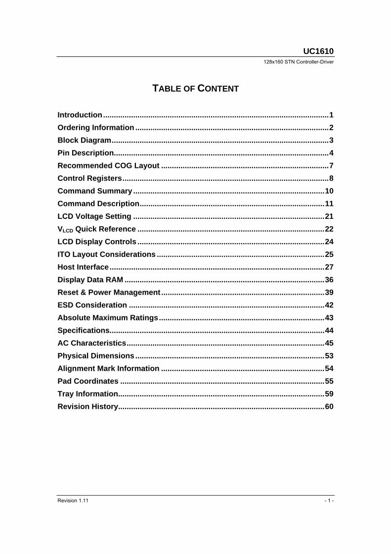
Introduction.........................................................................................................1
Ordering Information ..........................................................................................2
Block Diagram.....................................................................................................3
Pin Description....................................................................................................4
Recommended COG Layout ..............................................................................7
Control Registers................................................................................................8
Command Summary .........................................................................................10
Command Description......................................................................................11
LCD Voltage Setting .........................................................................................21
VLCD Quick Reference .......................................................................................22
LCD Display Controls .......................................................................................24
ITO Layout Considerations ..............................................................................25
Host Interface....................................................................................................27
Display Data RAM .............................................................................................36
Reset & Power Management ............................................................................39
ESD Consideration ...........................................................................................42
Absolute Maximum Ratings.............................................................................43
Specifications....................................................................................................44
AC Characteristics............................................................................................45
Physical Dimensions ........................................................................................53
Alignment Mark Information ............................................................................54
Pad Coordinates ...............................................................................................55
Tray Information................................................................................................59
Revision History................................................................................................60


UC1610 128x160 STN Controller-Driver
Revision 1.11 1
UC1610 Single-Chip, Ultra-Low Power 128COM x 160SEG Matrix Passive Color LCD Controller-Driver
INTRODUCTION UC1610 is an advanced high-voltage mixed-signal CMOS IC, especially designed for the display needs of ultra-low power hand-held devices.
This chip employs UltraChip’s unique DCC (Direct Capacitor Coupling) driver architecture to achieve near crosstalk free images, with well balanced gray shades.
In addition to low power COM and SEG drivers, UC1610 contains all necessary circuits for high-V LCD power supply, bias voltage generation, timing generation and graphics data memory.
Advanced circuit design techniques are employed to minimize external component counts and reduce connector size while achieving extremely low power consumption.
MAIN APPLICATIONS • Cellular Phones and other battery operated
palm top devices or portable Instruments
FEATURE HIGHLIGHTS • Single chip controller-driver for 128x160
matrix STN LCD with 4 gray shades.
• One software readable ID pin to support configurable vender identification.
• Partial scroll function and programmable data update window to support flexible manipulation of screen data.
• Support both row ordered and column ordered display buffer RAM access
• Support industry standard 2-wire, 3-wire, 4-wire serial bus (I2C, S9, S8, S8uc) and 8-bit/4-bit parallel bus (8080 or 6800).
• Special driver structure and gray shade modulation scheme. Consistent low power consumption under all display patterns.
• Fully programmable Mux Rate, partial display window, Bias Ratio and Line Rate allow many flexible power management options.
• Four software programmable frame rates up to 130Hz. Support the use of fast Liquid Crystal material for speedy LCD response.
• Software programmable 4 temperature compensation coefficients.
• On-chip Power-ON Reset and Software RESET command, make RST pin optional.
• Self-configuring 8x charge pump with on-chip pumping capacitors. Only 3 external capacitors are required to operate.
• Flexible data addressing/mapping schemes to support wide ranges of software models and LCD layout placements.
• Very low pin count (9~10 pins with S9 or I2C) allows exceptional image quality in COG format on conventional ITO glass.
• Many on-chip and I/O pad layout features to support optimized COG applications.
• VDD (digital) range: 1.8V ~ 3.3V VDD (analog) range: 2.6V ~ 3.3V LCD VOP range: 5.0V ~ 15V
• Available in gold bump dies Bump pitch: 50µM Bump gap: 17µM. Bump surface: >3,000µM2
ULTRACHIP
High-Voltage Mixed-Signal IC ©1999~2005
2 MP Specifications
ORDERING INFORMATION Part Number Versions Description UC1610iGAB Gold Bumped Die Bare die with gold bumps with I2C interface
General Notes APPLICATION INFORMATION For improved readability, the specification contains many application data points. When application information is given, it is advisory and does not form part of the specification for the device.
BARE DIE DISCLAIMER All die are tested and are guaranteed to comply with all data sheet limits up to the point of wafer sawing for a period of ninety (90) days from the date of UltraChip’s delivery. There is no post waffle saw/pack testing performed on individual die. Although the latest processes are utilized for wafer sawing and die pick-&-place into waffle pack carriers, UltraChip has no control of third party procedures in the handling, packing or assembly of the die. Accordingly, it is the responsibility of the customer to test and qualify their applications in which the die is to be used. UltraChip assumes no liability for device functionality or performance of the die or systems after handling, packing or assembly of the die.
USE OF I2C
The implementation of I2C is already included and tested in all silicon. However, unless I2C licensing obligation is executed satisfactorily, it is not legal to use UltraChip product for I2C applications. Unless I2C version is ordered from UltraChip, the customer will take the responsibility for all such licensing liabilities.
LIFE SUPPORT APPLICATIONS These devices are not designed for use in life support appliances, or systems where malfunction of these products can reasonably be expected to result in personal injuries. Customer using or selling these products for use in such applications do so at their own risk.
CONTENT DISCLAIMER UltraChip believes the information contained in this document to be accurate and reliable. However, it is subject to change without notice. No responsibility is assumed by UltraChip for its use, nor for infringement of patents or other rights of third parties. No part of this publication may be reproduced, or transmitted in any form or by any means without the prior consent of UltraChip Inc. UltraChip's terms and conditions of sale apply at all times.
CONTACT INFORMATION UltraChip Inc. (Headquarter) 2F, No. 70, Chowtze Street, Nei Hu District, Taipei 114, Taiwan, R. O. C.
Tel: +886 (2) 8797-8947 Fax: +886 (2) 8797-8910 Sales e-mail: [email protected] Web site: http://www.ultrachip.com
UC1610 128x160 STN Controller-Driver
Revision 1.11 3
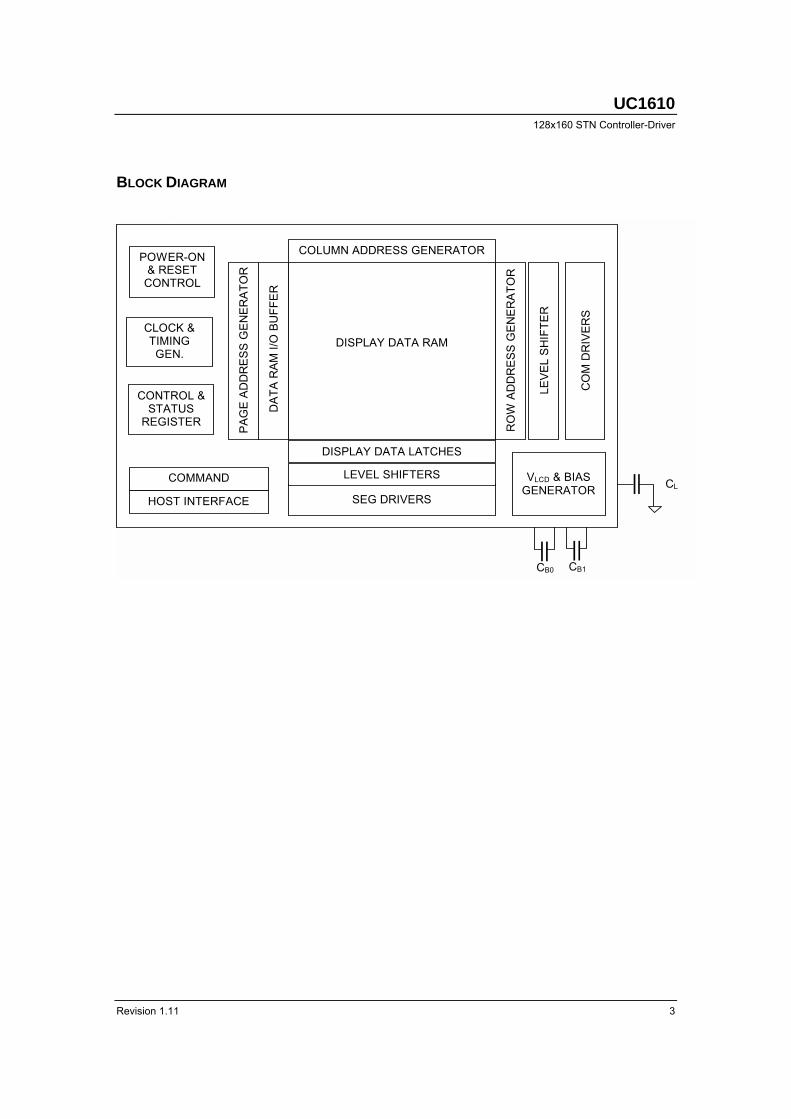
BLOCK DIAGRAM
CO
M D
RIV
ERS
SEG DRIVERS
POWER-ON & RESET
CONTROL
RO
W A
DD
RE
SS G
EN
ER
ATO
R
CLOCK & TIMING GEN.
HOST INTERFACE
CONTROL & STATUS
REGISTER
COMMAND
COLUMN ADDRESS GENERATOR
DISPLAY DATA RAM
DISPLAY DATA LATCHES
LEVEL SHIFTERS
LEV
EL S
HIF
TER
VLCD & BIAS
GENERATOR
PAG
E A
DD
RE
SS
GE
NE
RA
TOR
DA
TA R
AM
I/O
BU
FFE
R
CL
CB1 CB0

ULTRACHIP
High-Voltage Mixed-Signal IC ©1999~2005
4 MP Specifications
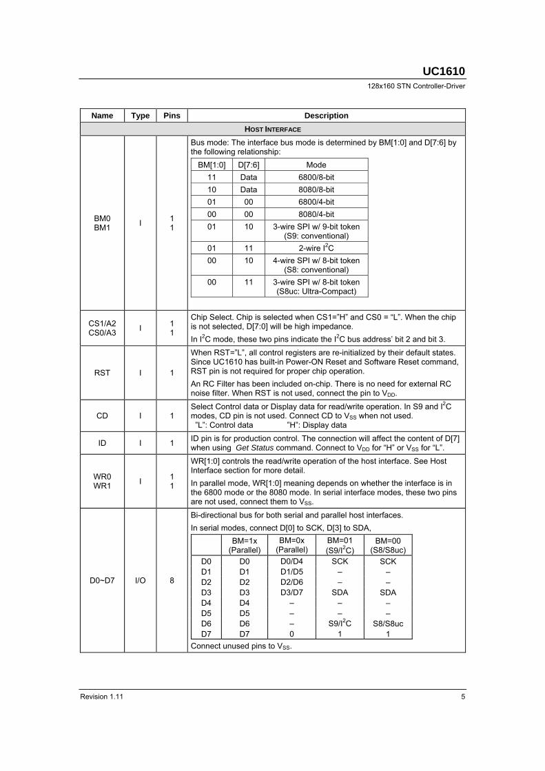
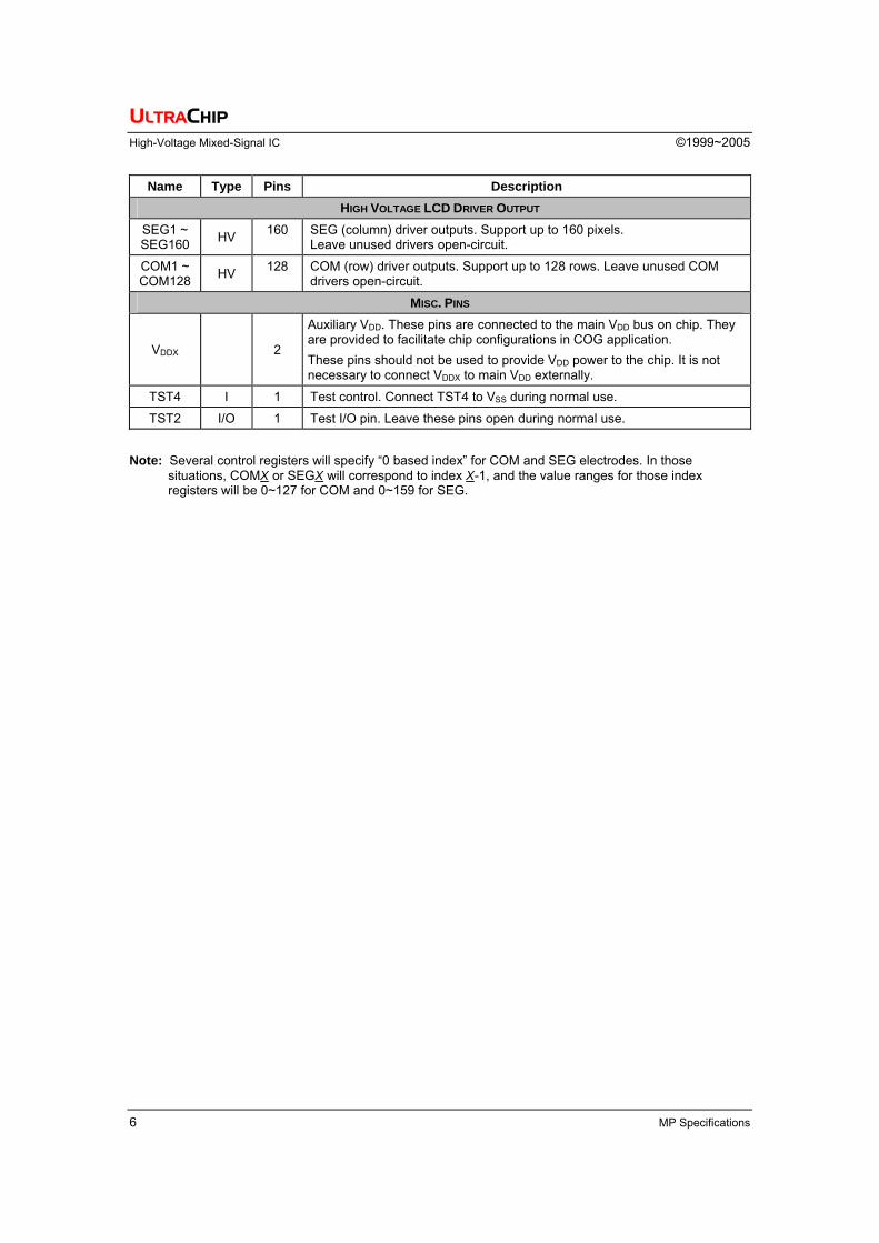
PIN DESCRIPTION Name Type Pins Description
MAIN POWER SUPPLY
VDD VDD2 VDD3
PWR 5 3 3
VDD2/VDD3 is the analog power supply and it should be connected to the same power source. VDD is the digital power supply and it should be connected to a voltage source that is no higher than VDD2/VDD3. Please maintain the following relationship:
VDD+1.3V VDD2/3 VDD Minimize the trace resistance for VDD and VDD2/VDD3.
VSS VSS2
GND 6 5
Ground. Connect VSS and VSS2 to the shared GND pin. Minimize the trace resistance for this node.
LCD POWER SUPPLY & VOLTAGE CONTROL
VBIAS I 1
This is the reference voltage to generate the actual SEG driving voltage. VBIAS can be used to fine tune VLCD by external variable resistors. Internal resistor network has been provided to simplify external trimming circuit. The following network is sufficient for most applications.
An internal RC filter is provided to filter noise on the VBIAS pin. When not use, it is OK to leave VBIAS open circuit. If noise starts to cause problem, connect a small bypass capacitor between VBIAS and VSS.
VB1+ VB1– VB0+ VB0–
PWR 9, 9 9, 9
LCD Bias Voltages. These are the voltage sources to provide SEG driving currents. These voltages are generated internally. Connect capacitors of CBX value between VBX+ and VBX–. The resistance of these traces directly affects the driving strength of SEG electrodes and impacts the image of the LCD module. Minimize the trace resistance is critical in achieving high quality image.
VLCDIN VLCDOUT PWR 2
2
High voltage LCD Power Supply. Connect these pins together. By-pass capacitor CL is optional. It can be connected between VLCD and VSS. When CL is used, keep the trace resistance under 300 Ohm.
NOTE
• Recommended capacitor values: CB: 150~250x LCD load capacitance or 2µF (2V), whichever is higher. CL: 0.06µF~0.3µF (25V) is appropriate for most applications.
1M/VR
VDD2/ VDD3
VBIAS
330K
UC1610 128x160 STN Controller-Driver
Revision 1.11 5
Name Type Pins Description HOST INTERFACE
BM0 BM1 I 1
1
Bus mode: The interface bus mode is determined by BM[1:0] and D[7:6] by the following relationship:
BM[1:0] D[7:6] Mode 11 Data 6800/8-bit 10 Data 8080/8-bit 01 00 6800/4-bit 00 00 8080/4-bit 01 10 3-wire SPI w/ 9-bit token
(S9: conventional) 01 11 2-wire I2C 00 10 4-wire SPI w/ 8-bit token
(S8: conventional) 00 11 3-wire SPI w/ 8-bit token
(S8uc: Ultra-Compact)
CS1/A2 CS0/A3 I 1
1
Chip Select. Chip is selected when CS1=”H” and CS0 = “L”. When the chip is not selected, D[7:0] will be high impedance. In I2C mode, these two pins indicate the I2C bus address’ bit 2 and bit 3.
RST I 1
When RST=”L”, all control registers are re-initialized by their default states. Since UC1610 has built-in Power-ON Reset and Software Reset command, RST pin is not required for proper chip operation. An RC Filter has been included on-chip. There is no need for external RC noise filter. When RST is not used, connect the pin to VDD.
CD I 1 Select Control data or Display data for read/write operation. In S9 and I2C modes, CD pin is not used. Connect CD to VSS when not used. ”L”: Control data ”H”: Display data
ID I 1 ID pin is for production control. The connection will affect the content of D[7] when using Get Status command. Connect to VDD for “H” or VSS for “L”.
WR0 WR1 I 1
1
WR[1:0] controls the read/write operation of the host interface. See Host Interface section for more detail. In parallel mode, WR[1:0] meaning depends on whether the interface is in the 6800 mode or the 8080 mode. In serial interface modes, these two pins are not used, connect them to VSS.
D0~D7 I/O 8
Bi-directional bus for both serial and parallel host interfaces. In serial modes, connect D[0] to SCK, D[3] to SDA,
BM=1x (Parallel)
BM=0x (Parallel)
BM=01 (S9/I2C)
BM=00 (S8/S8uc)
D0 D0 D0/D4 SCK SCK D1 D1 D1/D5 – – D2 D2 D2/D6 – – D3 D3 D3/D7 SDA SDA D4 D4 – – – D5 D5 – – – D6 D6 – S9/I2C S8/S8uc D7 D7 0 1 1
Connect unused pins to VSS.
ULTRACHIP
High-Voltage Mixed-Signal IC ©1999~2005
6 MP Specifications
Name Type Pins Description HIGH VOLTAGE LCD DRIVER OUTPUT
SEG1 ~ SEG160 HV 160 SEG (column) driver outputs. Support up to 160 pixels.
Leave unused drivers open-circuit.
COM1 ~ COM128 HV 128 COM (row) driver outputs. Support up to 128 rows. Leave unused COM
drivers open-circuit.
MISC. PINS
VDDX 2
Auxiliary VDD. These pins are connected to the main VDD bus on chip. They are provided to facilitate chip configurations in COG application. These pins should not be used to provide VDD power to the chip. It is not necessary to connect VDDX to main VDD externally.
TST4 I 1 Test control. Connect TST4 to VSS during normal use.
TST2 I/O 1 Test I/O pin. Leave these pins open during normal use.
Note: Several control registers will specify “0 based index” for COM and SEG electrodes. In those situations, COMX or SEGX will correspond to index X-1, and the value ranges for those index registers will be 0~127 for COM and 0~159 for SEG.
UC1610 128x160 STN Controller-Driver
Revision 1.11 7
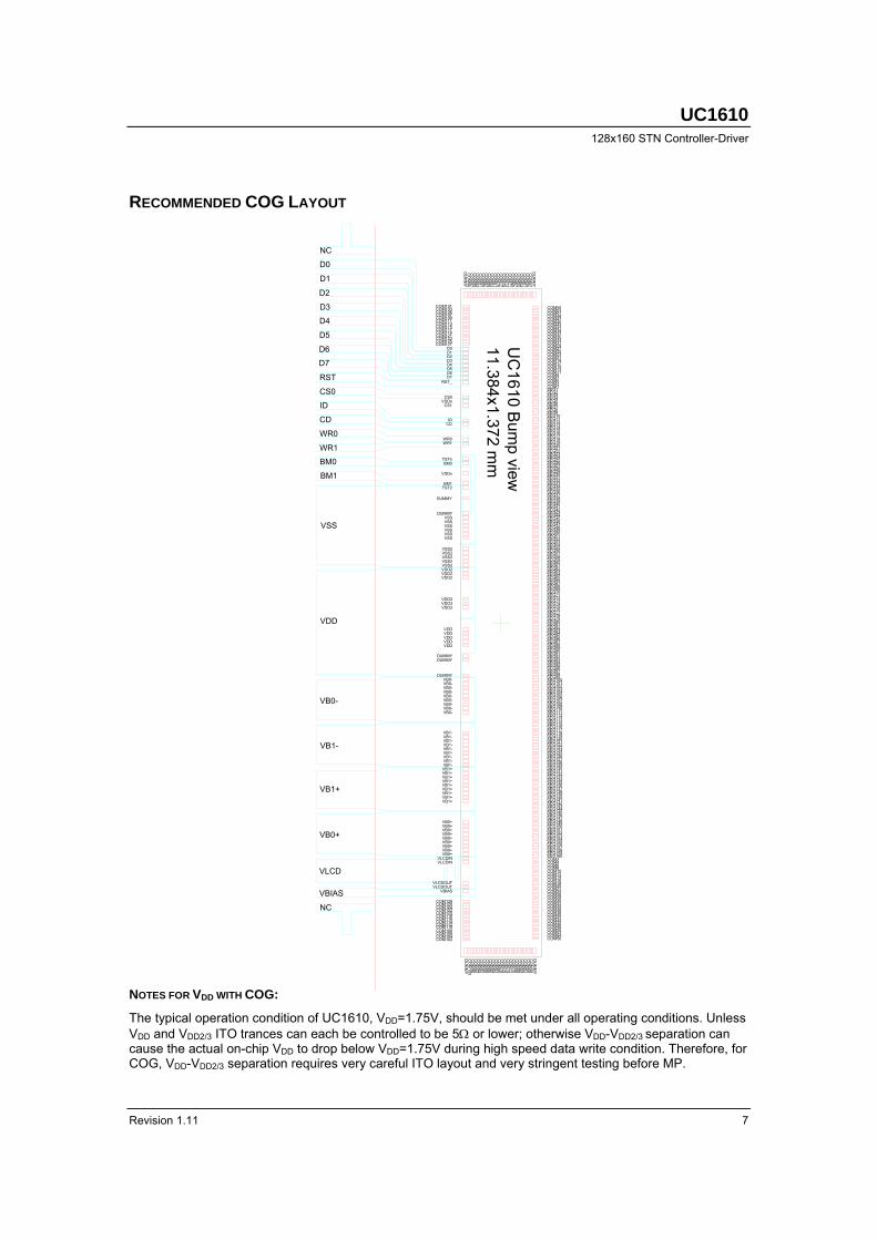
RECOMMENDED COG LAYOUT
NC
D0
D1
D2
D3
D4
D5
D6
D7
RST
CS0
ID
CD
WR0
WR1
BM0
BM1
VB0-
VB1-
VB1+
VSS
VDD
NC
VBIAS
VLCD
VB0+
11.384x1.372 mm
SEG1SEG2SEG3SEG4
COM56COM54COM52COM50COM48COM46COM44COM42COM40COM38COM36COM34COM32COM30COM28COM26COM24COM22COM20COM18COM16COM14COM12COM10COM8COM6COM4COM2
CO
M58
DU
MM
Y
CO
M62
CO
M64
CO
M60
CO
M72
CO
M70
CO
M78
CO
M76
CO
M74
CO
M68
CO
M66
SEG7SEG8SEG9SEG10SEG11SEG12SEG13SEG14SEG15SEG16SEG17SEG18SEG19SEG20SEG21SEG22SEG23SEG24SEG25SEG26SEG27SEG28SEG29SEG30SEG31SEG32SEG33SEG34SEG35SEG36SEG37SEG38SEG39SEG40SEG41SEG42SEG44SEG45SEG46SEG47SEG48SEG49SEG50SEG51SEG52SEG53SEG54SEG55SEG56SEG57SEG58SEG59SEG60SEG61SEG62SEG63SEG64SEG65SEG66SEG67SEG68SEG69SEG70SEG71SEG72SEG73SEG74SEG75SEG76SEG77SEG78SEG79
SEG43
SEG5SEG6
CO
M86
CO
M84
CO
M92
CO
M90
CO
M88
CO
M100
CO
M98
DU
MM
Y
CO
M96
CO
M94
VB0+VB0+VB0+
VLCDINVLCDIN
VBIAS
VLCDOUTVLCDOUT
COM128COM126COM124COM122COM120COM118COM116COM114COM112COM110COM108COM106COM104COM102
VB1+VB1+VB1+
VB0+VB0+VB0+VB0+VB0+
VB1-VB1-VB1-VB1-VB1-VB1-VB1-VB1-VB1+VB1+VB1+VB1+VB1+VB1+
VB0-VB0-VB0-VB0-VB0-VB0-VB0-VB0-
VDDVDDVDDVDDVDD
DUMMYDUMMY
DUMMYVB0-
VB1-
VB0+
CO
M82
CO
M80
SEG82SEG83SEG84SEG85SEG86SEG87SEG88SEG89SEG90SEG91SEG92SEG93SEG94SEG95SEG96SEG97SEG98SEG99SEG100SEG101SEG102SEG103SEG104SEG105SEG106SEG107SEG108SEG109SEG110SEG111SEG112SEG113SEG114SEG115SEG116SEG117SEG119SEG120SEG121SEG122SEG123SEG124SEG125SEG126SEG127SEG128SEG129SEG130SEG131SEG132SEG133SEG134SEG135SEG136SEG137SEG138SEG139SEG140SEG141SEG142SEG143SEG144SEG145SEG146SEG147SEG148SEG149SEG150SEG151SEG152SEG153SEG154
SEG118
SEG157SEG158SEG159SEG160
COM1COM3COM5COM7COM9COM11COM13COM15COM17COM19COM21COM23COM25COM27COM29COM31COM33COM35COM37COM39COM41COM43COM45COM47COM49COM51COM53COM55
CO
M57
DU
MM
Y
CO
M61
CO
M63
CO
M59
CO
M69
CO
M75
CO
M77
CO
M71
CO
M73
CO
M65
CO
M67
SEG155SEG156
VDD2VDD2
VDD3VDD3VDD3
VSSVSSVSSVSSVSSVSS
VSS2VSS2VSS2VSS2VSS2VDD2
BM0
VDDx
BM1TST2
DUMMY
IDCD
WR0WR1
TST4
DUMMY
CO
M81
CO
M83
CO
M89
CO
M91
CO
M85
CO
M87
CO
M95
CO
M97
CO
M99
DU
MM
Y
CO
M93
D1D2D3D4D5D6D7
RST_
CS0
D0
COM101COM103COM105COM107COM109COM111COM113COM115COM117COM119COM121COM123COM125COM127
VDDxCS1
CO
M79
SEG80SEG81
UC
1610 Bum
p view
NOTES FOR VDD WITH COG:
The typical operation condition of UC1610, VDD=1.75V, should be met under all operating conditions. Unless VDD and VDD2/3 ITO trances can each be controlled to be 5Ω or lower; otherwise VDD-VDD2/3 separation can cause the actual on-chip VDD to drop below VDD=1.75V during high speed data write condition. Therefore, for COG, VDD-VDD2/3 separation requires very careful ITO layout and very stringent testing before MP.

ULTRACHIP
High-Voltage Mixed-Signal IC ©1999~2005
8 MP Specifications
CONTROL REGISTERS UC1610 contains registers which control the chip operation. These registers can be modified by commands. The following table is a summary of the control registers, their meanings and their default values. Commands supported by UC1610 will be described in the next two sections. First, a summary table, followed by a detailed instruction-by-instruction description.
Name: The Symbolic reference of the register. Note that, some symbol name refers to bits (flags) within another register.
Default: Numbers shown in Bold font are default values after Power-Up-Reset and System-Reset.
Name Bits Default Description
SL 7 0H Scroll Line. Scroll the displayed image up by SL rows. The valid SL value is between 0 (for no scrolling) and (127– 2xFL). Setting SL outside of this range causes undefined effect on the displayed image.
FL 4 0H Fixed Lines. The first FLx2 lines of each frame are fixed and are not affected by scrolling (SL). When FL is non-zero, the screen is effectively separated into two regions: one scrollable, one non-scrollable. When partial display mode is activated, the display of these 2xFL lines are also controlled by LC[0].
CR 8 0H Return Column Address. Useful for cursor implementation.
CA 8 0H Display Data RAM Column Address (Used in Host to Display Data RAM access)
PA 5 0H Display Data RAM Page Address (Used in Host to Display Data RAM access)
BR 2 2H Bias Ratio. The ratio between VLCD and VBIAS. 00b: 5 01b: 10 10b: 11 11b: 12
TC 2 0H Temperature Compensation (per oC) 00b: -0.05% 01b: -0.10% 10b: -0.15% 11b: -0.20%
PM 8 B2H Electronic Potentiometer to fine tune VBIAS and VLCD OM 2 – Operating Modes (Read only)
00b: Reset 01b: (Not used) 10b: Sleep 11b: Normal
ID 1 PIN Access the connected status of ID pin.
RS 1 Reset in progress. Host Interface not ready
PC 4 DH Power Control. PC[1:0]: 00b: LCD: 16nF 01b: LCD: 16~21nF 10b: LCD: 21~28nF 11b: LCD: 28~38nF PC[3:2]: 00b: External VLCD 01b: Internal VLCD (6X pump, low VLCD, only used when BR=5) 10b: Internal VLCD (7X pump) 11b: Internal VLCD (8X pump, standard)
DC 3 00H Display Control: DC[0]: PXV: Pixels Inverse. Bit-wise data inversion. (Default 0: OFF) DC[1]: APO: All Pixels ON (Default 0: OFF) DC[2]: Display ON/OFF (Default 0: OFF)
UC1610 128x160 STN Controller-Driver
Revision 1.11 9
Name Bits Default Description
AC 5 01H Address Control: AC[0]: WA: Automatic column/page Wrap Around (Default 1: ON) AC[1]: Auto-Increment order 0: Column (CA) first 1: Row (PA) first AC[2]: PID: PA (Page Address) auto increment direction (L:+1 H:-1) AC[3]: CUM: Cursor update mode, (Default 0: OFF) when CUM=1, CA increment on write only, wrap around suspendedAC[4] : Window Program Enable 0 : Disable 1 : Enable
WPC0 8 00H Window program starting column address. Value range: 0 ~159.
WPP0 5 00H Window program starting Page Address. Value range: 0~31.
WPC1 8 9FH Window program ending column address. Value range: 0~159.
WPP1 5 1FH Window program ending Page Address. Value range: 0~31.
CEN DST DEN
7 7 7
7FH 00H 7FH
COM scanning end (last COM with full line cycle, 0 based index) Display start (first COM with active scan pulse, 0 based index) Display end (last COM with active scan pulse, 0 based index) Please maintain the following relationship: CEN = the actual number of pixel rows on the LCD - 1 CEN DEN DST+ 9
LC 9 008H LCD Control: LC[0]: Enable the first FLx2 lines in partial display mode (Default OFF). LC[1]: MX, Mirror X. SEG/Column sequence inversion (Default: OFF) LC[2]: MY, Mirror Y. COM/Row sequence inversion (Default: OFF) LC[4:3]: Line Rate (Klps: Kilo-Line-per-second) 00b: 12.1 Klps (95fps) 01b: 13.4 Klps (105fps) 10b: 14.7 Klps (115fps) 11b: 16.6 Klps (130fps) (Frame-Rate = Line-Rate / Mux-Rate, Frame rate at 128 is listed) LC[6:5] : Gray-Shade control. Control the difference of percentage between data “01” and “10” 00b: 24% 01b: 29% 10b: 36% 11b: 40% LC[8:7] : Partial Display Control 00b: Disable Mux-Rate = CEN+1 (DST, DEN not used) 10b: Enable Mux-Rate = CEN+1 11b: Enabled Mux-Rate = DEN-DST+1
APC0 APC1
8 8
-- -- Advanced Product Configuration. For UltraChip only. Do NOT use.
ULTRACHIP
High-Voltage Mixed-Signal IC ©1999~2005
10 MP Specifications
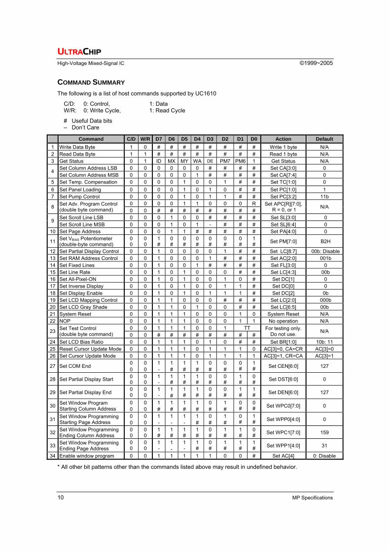
COMMAND SUMMARY The following is a list of host commands supported by UC1610
C/D: 0: Control, 1: Data W/R: 0: Write Cycle, 1: Read Cycle
# Useful Data bits – Don’t Care
Command C/D W/R D7 D6 D5 D4 D3 D2 D1 D0 Action Default 1 Write Data Byte 1 0 # # # # # # # # Write 1 byte N/A 2 Read Data Byte 1 1 # # # # # # # # Read 1 byte N/A 3 Get Status 0 1 ID MX MY WA DE PM7 PM6 1 Get Status N/A
Set Column Address LSB 0 0 0 0 0 0 # # # # Set CA[3:0] 0 4 Set Column Address MSB 0 0 0 0 0 1 # # # # Set CA[7:4] 0
5 Set Temp. Compensation 0 0 0 0 1 0 0 1 # # Set TC[1:0] 0 6 Set Panel Loading 0 0 0 0 1 0 1 0 # # Set PC[1:0] 1 7 Set Pump Control 0 0 0 0 1 0 1 1 # # Set PC[3:2] 11b
0 0 0 0 1 1 0 0 0 R8 Set Adv. Program Control (double byte command) 0 0 # # # # # # # #
Set APC[R][7:0], R = 0, or 1 N/A
Set Scroll Line LSB 0 0 0 1 0 0 # # # # Set SL[3:0] 0 9 Set Scroll Line MSB 0 0 0 1 0 1 - # # # Set SL[6:4] 0
10 Set Page Address 0 0 0 1 1 # # # # # Set PA[4:0] 0
11 Set VBIAS Potentiometer (double-byte command)
0 0
0 0
1 #
0#
0#
0#
0#
0 #
0#
1# Set PM[7:0] B2H
12 Set Partial Display Control 0 0 1 0 0 0 0 1 # # Set LC[8:7] 00b: Disable13 Set RAM Address Control 0 0 1 0 0 0 1 # # # Set AC[2:0] 001b 14 Set Fixed Lines 0 0 1 0 0 1 # # # # Set FL[3:0] 0 15 Set Line Rate 0 0 1 0 1 0 0 0 # # Set LC[4:3] 00b 16 Set All-Pixel-ON 0 0 1 0 1 0 0 1 0 # Set DC[1] 0 17 Set Inverse Display 0 0 1 0 1 0 0 1 1 # Set DC[0] 0 18 Set Display Enable 0 0 1 0 1 0 1 1 1 # Set DC[2] 0b 19 Set LCD Mapping Control 0 0 1 1 0 0 0 # # # Set LC[2:0] 000b 20 Set LCD Gray Shade 0 0 1 1 0 1 0 0 # # Set LC[6:5] 00b 21 System Reset 0 0 1 1 1 0 0 0 1 0 System Reset N/A 22 NOP 0 0 1 1 1 0 0 0 1 1 No operation N/A
0 0 1 1 1 0 0 1 TT 23 Set Test Control (double byte command) 0 0 # # # # # # # #
For testing only. Do not use. N/A
24 Set LCD Bias Ratio 0 0 1 1 1 0 1 0 # # Set BR[1:0] 10b: 11 25 Reset Cursor Update Mode 0 0 1 1 1 0 1 1 1 0 AC[3]=0, CA=CR AC[3]=0 26 Set Cursor Update Mode 0 0 1 1 1 0 1 1 1 1 AC[3]=1, CR=CA AC[3]=1
27 Set COM End 0 0
0 0
1 -
1#
1#
1#
0#
0 #
0#
1# Set CEN[6:0] 127
28 Set Partial Display Start 0 0
0 0
1 -
1#
1#
1#
0#
0 #
1#
0# Set DST[6:0] 0
29 Set Partial Display End 0 0
0 0
1 -
1#
1#
1#
0#
0 #
1#
1# Set DEN[6:0] 127
30 Set Window Program Starting Column Address
0 0
0 0
1 #
1#
1#
1#
0#
1 #
0#
0# Set WPC0[7:0] 0
31 Set Window Programming Starting Page Address
0 0
0 0
1 -
1-
1-
1#
0#
1 #
0#
1# Set WPP0[4:0] 0
32 Set Window Programming Ending Column Address
0 0
0 0
1 #
1#
1#
1#
0#
1 #
1#
0# Set WPC1[7:0] 159
33 Set Window Programming Ending Page Address
0 0
0 0
1 -
1-
1-
1#
0#
1 #
1#
1# Set WPP1[4:0] 31
34 Enable window program 0 0 1 1 1 1 1 0 0 # Set AC[4] 0: Disable
* All other bit patterns other than the commands listed above may result in undefined behavior.

UC1610 128x160 STN Controller-Driver
Revision 1.11 11
COMMAND DESCRIPTION
(1) WRITE DATA TO DISPLAY MEMORY
Action C/D W/R D7 D6 D5 D4 D3 D2 D1 D0 Write data 1 0 8bits data write to DDRAM
(2) READ DATA FROM DISPLAY MEMORY
Action C/D W/R D7 D6 D5 D4 D3 D2 D1 D0 Read data 1 1 8bits data from DDRAM
Write/Read Data Byte (command 1, 2 ) operation use internal Page Address register (PA) and Column Address register (CA). Four rows of LCD pixel image are defined as one page in DDRAM. Each column of pixel corresponds to one column of DDRAM data. PA and CA registers can be programmed by issuing Set Page Address and Set Column Address commands. If wrap-around (WA, AC[0]) is OFF (0), CA will stop incrementing after reaching the CA boundary, and system programmers need to set the values of PA and CA explicitly. If WA is ON (1), when CA reaches end of column address, CA will be reset to 0 and PA will be incremented or decremented, depending on the setting of Row Increment Direction (PID, AC[2]). When PA reaches the boundary of RAM (i.e. PA = 0 or 31), PA will be wrapped around to the other end of RAM and continue.
(3) GET STATUS
Action C/D W/R D7 D6 D5 D4 D3 D2 D1 D0 Get Status 0 1 ID MX MY WA DE PM7 PM6 1
Status flag definitions:
ID: Provide access to ID pin connection status. MX: Status of register LC[1], mirror X. MY: Status of register LC[2], mirror Y. WA: Status of register AC[0]. Automatic column/page wrap around. DE: Display enable flag. DE=1 when display is enabled
(4) SET COLUMN ADDRESS
Action C/D W/R D7 D6 D5 D4 D3 D2 D1 D0 Set Column Address LSB CA[3:0] 0 0 0 0 0 0 CA3 CA2 CA1 CA0 Set Column Address MSB CA[7:4] 0 0 0 0 0 1 CA7 CA6 CA5 CA4
Set DDRAM column address for read/write access. Each CA corresponds to one individual SEG electrode.
CA value range: 0~159
(5) SET TEMPERATURE COMPENSATION
Action C/D W/R D7 D6 D5 D4 D3 D2 D1 D0 Set Temperature Comp. TC[1:0] 0 0 0 0 1 0 0 1 TC1 TC0
Set VBIAS temperature compensation coefficient (%-per-degree-C)
Temperature compensation curve definition: 00b= -0.05%/oC 01b= -0.10%/oC 10b= -0.15%/oC 11b= -0.20%/oC
ULTRACHIP
High-Voltage Mixed-Signal IC ©1999~2005
12 MP Specifications
(6) SET PANEL LOADING
Action C/D W/R D7 D6 D5 D4 D3 D2 D1 D0 Set Panel Loading PC[1:0] 0 0 0 0 1 0 1 0 PC1 PC0
Set PC[1:0] according to the capacitance loading of LCD panel.
Panel loading definition: 00b 16nF 01b=16~21nF 10b=21~28nF 11b=28~38nF
(7) SET PUMP CONTROL
Action C/D W/R D7 D6 D5 D4 D3 D2 D1 D0 Set Pump Control PC[3:2] 0 0 0 0 1 0 1 1 PC3 PC2
Set PC[3:2] to program the build-in charge pump stages.
Pump control definition:
00b=External VLCD 01b= Internal VLCD (6X pump, for BR=5) 01b= Internal VLCD (7X pump) 11b= Internal VLCD (8X pump, standard)
(8) SET ADVANCED PROGRAM CONTROL
Action C/D W/R D7 D6 D5 D4 D3 D2 D1 D0 0 0 0 0 1 1 0 0 0 R Set APC[R]
(Double byte command) 0 0 APC register parameter For UltraChip only. Please do NOT use.
(9) SET SCROLL LINE
Action C/D W/R D7 D6 D5 D4 D3 D2 D1 D0 Set Scroll Line LSB SL[3:0] 0 0 0 1 0 0 SL3 SL2 SL1 SL0 Set Scroll Line MSB SL[6:4] 0 0 0 1 0 1 - SL6 SL5 SL4
Set the scroll line number.
Scroll line setting will scroll the displayed image up by SL rows. The valid value for SL is between 0 (no scrolling) and (127-2xFL). FL is the register value programmed by Set Fixed Lines command.
SL=0 SL=N
(10) SET PAGE ADDRESS
Action C/D W/R D7 D6 D5 D4 D3 D2 D1 D0 Set Page Address PA [4:0] 0 0 0 1 1 PA4 PA3 PA2 PA1 PA0
Set DDRAM Page Address for read/write access.
Possible value = 0~31
Image row 0
Image row N
Image row 127
Image row N
……….
Image row 127
Image row 0
………
image row N-1
UC1610 128x160 STN Controller-Driver
Revision 1.11 13
(11) SET VBIAS POTENTIOMETER
Action C/D W/R D7 D6 D5 D4 D3 D2 D1 D0 0 0 1 0 0 0 0 0 0 1 Set VBIAS Potentiometer. PM [7:0]
(Double byte command) 0 0 PM7 PM6 PM5 PM4 PM3 PM2 PM1 PM0 Program VBIAS Potentiometer (PM[7:0]). See section LCD VOLTAGE SETTING for more detail.
Effective range: 0 ~ 255
(12) SET PARTIAL DISPLAY CONTROL
Action C/D W/R D7 D6 D5 D4 D3 D2 D1 D0 Set Partial Display Enable LC [8:7] 0 0 1 0 0 0 0 1 LC8 LC7
This command is used to enable partial display function.
LC[8:7] : 00b: Disable Partial Display, Mux-Rate = CEN+1 (DST, DEN not used.) 10b: Enable Partial Display, Mux-Rate = CEN+1 11b: Enable Partial Display, Mux-Rate = DEN-DST+1
(13) SET RAM ADDRESS CONTROL
Action C/D W/R D7 D6 D5 D4 D3 D2 D1 D0 Set AC [2:0] 0 0 1 0 0 0 1 AC2 AC1 AC0
Program registers AC[2:0] for RAM address control.
AC[0]: WA, Automatic column/page wrap around. 0: CA or PA (depends on AC[1]= 0 or 1) will stop incrementing after reaching boundary 1: CA or PA (depends on AC[1]= 0 or 1) will restart, and PA or CA will increment by one step.
AC[1]: Auto-Increment order 0 : column (CA) increment (+1) first until CA reaches CA boundary, then PA will increment by (+/-1). 1 : row (PA) increment (+/-1) first until PA reach PA boundary, then CA will increment by (+1) .
AC[2]: PID, Page Address (PA) auto increment direction ( 0/1 = +/- 1 ) When WA=1 and CA reaches CA boundary, PID controls whether Page Address will be adjusted by +1 or -1.
AC[2:0] controls the auto-increment behavior of CA and PA. When Window Program is enabled (AC[4]=ON), see command description (32) ~ (36) for more details. When Window Program is disabled (AC[4]=OFF), the behavior of CA, PA auto-increment is the same as WPC[1:0] and WPP[1:0] values are the default values and AC[4]=ON.
ULTRACHIP
High-Voltage Mixed-Signal IC ©1999~2005
14 MP Specifications
(14) SET FIXED LINES
Action C/D W/R D7 D6 D5 D4 D3 D2 D1 D0 Set Fixed Lines FL [3:0] 0 0 1 0 0 1 FL3 FL2 FL1 FL0
The fixed line function is used to implement the partial scroll function by dividing the screen into scroll and fixed area. Set Fixed Lines command will define the fixed area, which will not be affected by the SL scroll function. The fixed area covers the top 2xFL rows for mirror Y (MY) is 0 and bottom 2xFL rows for MY=1. One example of the visual effect on LCD is illustrated in the figure below.
MY = 0 MY = 1
(15) SET LINE RATE
Action C/D W/R D7 D6 D5 D4 D3 D2 D1 D0 Set Line Rate LC [4:3] 0 0 1 0 1 0 0 0 LC4 LC3
Program LC [4:3] for line rate setting (Frame-Rate = Line-Rate / Mux-Rate). The line rate is automatically scaled down by 1/2 and 1/4 at Mux-Rate = 56 and 24.
The following are line rates at Mux Rate = 57~128.
LC[4:3]: 00b: 12.1 Klps 01b: 13.4 Klps 10b: 14.7 Klps 11b: 16.6 Klps (Klps: Kilo-Line-per-second)
(16) SET ALL PIXEL ON
Action C/D W/R D7 D6 D5 D4 D3 D2 D1 D0 Set All Pixel ON DC [1] 0 0 1 0 1 0 0 1 0 DC1
Set DC[1] to force all SEG drivers to output ON signals. This function has no effect on the existing data stored in display RAM.
(17) SET INVERSE DISPLAY
Action C/D W/R D7 D6 D5 D4 D3 D2 D1 D0 Set Inverse Display DC [0] 0 0 1 0 1 0 0 1 1 DC0
Set DC[0] to force all SEG drivers to output the inverse of the data (bit-wise) stored in display RAM. This function has no effect on the existing data stored in display RAM.
Fixed area 1
(2xFL)
Scroll area
128
1
Scroll area
Fixed area
(2xFL) 128

UC1610 128x160 STN Controller-Driver
Revision 1.11 15
(18) SET DISPLAY ENABLE
Action C/D W/R D7 D6 D5 D4 D3 D2 D1 D0 Set Display Enable DC [2] 0 0 1 0 1 0 1 1 1 DC2
This command is for programming register DC[2].
When DC[2] is set to 0, the IC will put itself into Sleep mode. All drivers, voltage generation circuit and timing circuit will be halted to conserve power. When any of the DC[2] bits is set to 1, UC1610 will first exit from Sleep Mode, restore the power and then turn on COM drivers and SEG drivers. There is no other explicit user action or timing sequence required to enter or exit the Sleep mode.
(19) SET LCD MAPPING CONTROL
Action C/D W/R D7 D6 D5 D4 D3 D2 D1 D0 Set LCD Mapping Control LC [2:0] 0 0 1 1 0 0 0 MY MX LC0
This command is used for program LC[2:0] for COM (row) mirror (MY), SEG (column) mirror (MX).
LC2 controls Mirror Y (MY): MY is implemented by reversing the mapping order between RAM and COM electrodes. The data stored in RAM is not affected by MY command. MY will have immediate effect on the display image.
LC1 controls Mirror X (MX): MX is implemented by selecting the CA or 127-CA as write/read (from host interface) display RAM column address so this function will only take effect after rewriting the RAM data.
LC0 controls whether the soft icon section (0~ 2xFL) is display or not during partial display mode.
(20) SET LCD GRAY SHADE
Action C/D W/R D7 D6 D5 D4 D3 D2 D1 D0 Set LCD Gray Shade [6:5] 0 0 1 1 0 1 0 0 LC6 LC5
Program gray scale register (LC[6:5]). This register controls the voltage RMS separation between the two gray shade levels (data “01” and data “10”)
00b=24% 01b=29% 10b=36% 11b=40%
(21) SYSTEM RESET
Action C/D W/R D7 D6 D5 D4 D3 D2 D1 D0 System Reset 0 0 1 1 1 0 0 0 1 0
This command will activate the system reset. Control register values will be reset to their default values. Data stored in RAM will not be affected.
(22) NOP
Action C/D W/R D7 D6 D5 D4 D3 D2 D1 D0 No Operation 0 0 1 1 1 0 0 0 1 1
This command is used for “no operation”.
(23) SET TEST CONTROL
Action C/D W/R D7 D6 D5 D4 D3 D2 D1 D0 0 0 1 1 1 0 0 1 TT Set TT
(Double byte command) 0 0 Testing parameter This command is used for UltraChip production testing. Please do not use.
ULTRACHIP
High-Voltage Mixed-Signal IC ©1999~2005
16 MP Specifications
(24) SET LCD BIAS RATIO
Action C/D W/R D7 D6 D5 D4 D3 D2 D1 D0 Set Bias Ratio BR [1:0] 0 0 1 1 1 0 1 0 BR1 BR0
Bias ratio definition: 00b = 5 01b = 10 10b = 11 11b = 12
(25) RESET CURSOR UPDATE MODE
Action C/D W/R D7 D6 D5 D4 D3 D2 D1 D0 Set AC[3]=0 CA=CR 0 0 1 1 1 0 1 1 1 AC3
This command is used to reset cursor update mode function.
(26) SET CURSOR UPDATE MODE
Action C/D W/R D7 D6 D5 D4 D3 D2 D1 D0 Set AC[3]=1 CR=CA 0 0 1 1 1 0 1 1 1 AC3
This command is used for set cursor update mode function. When cursor update mode sets, UC1610 will update register CR with the value of register CA. The column address CA will increment with write RAM data operation but the address wraps around will be suspended no matter what WA setting is. However, the column address will not increment in read RAM data operation.
The set cursor update mode can be used to implement “write after read RAM” function. The column address (CA) will be restored to the value, which is before the set cursor update mode command, when reset cursor update mode.
The purpose of this pair of commands and their features is to support “write after read” function for cursor implementation.
(27) SET COM END
Action C/D W/R D7 D6 D5 D4 D3 D2 D1 D0 0 0 1 1 1 1 0 0 0 1 Set CEN
(Double-byte command) 0 0 CEN register parameter
This command programs the ending COM electrode. CEN defines the number of used COM electrodes, and it should correspond to the number of pixel-rows in the LCD.
(28) SET DISPLAY START
Action C/D W/R D7 D6 D5 D4 D3 D2 D1 D0 0 0 1 1 1 1 0 0 1 0 Set DST
(Double-byte command) 0 0 DST register parameter
This command programs the starting COM electrode, which has been assigned a full scanning period, and which will output an active COM scanning pulse.

UC1610 128x160 STN Controller-Driver
Revision 1.11 17
(29) SET DISPLAY END
Action C/D W/R D7 D6 D5 D4 D3 D2 D1 D0 0 0 1 1 1 1 0 0 1 1 Set DEN
(Double-byte command) 0 0 DEN register parameter
This command programs the ending COM electrode, which has been assigned a full scanning period, and which will output an active COM scanning pulse.
CEN, DST DEN are 0-based index of COM electrodes. They control only the COM electrode activity, and do not affect the mapping of display RAM to each COM electrodes. The image displayed by each pixel row is therefore not affected by the setting of these three registers.
When LC[8]=1, two partial display modes are possible with UC1610: LC[7]=1: ON-OFF only, ultra-low-power mode (if Mux-Rate 32, set BR=5, PC[3:2]=01b). LC[7]=0: Full gray shade low power mode (BR and PM stays the same)
When LC[8:7]=11b, the Mux-Rate is narrowed down to just the range between DST and DEN. When Mux-Rate is under 32, set BR=5, PC[3:2]=01b, and adjust PM to reduce VLCD and achieve the lowest power consumption. When LC[8:7]=10b, the Mux-Rate is still CEN+1. This is achieved by suppressing only the scanning pulses, but not the scanning time slots, for COM electrodes that is outside of DST~DEN. Under this mode, the gray-scale quality of the display is preserved, while the power can be reduced significantly. In either case, DST/DEN defines a small subsection of the display which will remain active while shutting down all the rest of the display to conserve energy.
0
DST
DEN Pulse Disable:
CEN Pulse Enable:
Not Scanned: 127

ULTRACHIP
High-Voltage Mixed-Signal IC ©1999~2005
18 MP Specifications
(30) SET WINDOW PROGRAM STARTING COLUMN ADDRESS
Action C/D W/R D7 D6 D5 D4 D3 D2 D1 D0 0 0 1 1 1 1 0 1 0 0 Set WPC0
(Double-byte command) 0 0 WPC0[7:0] register parameter
This command is to program the starting column address of RAM program window.
(31) SET WINDOW PROGRAM STARTING PAGE ADDRESS
Action C/D W/R D7 D6 D5 D4 D3 D2 D1 D0 0 0 1 1 1 1 0 1 0 1
Set WPP0 (Double-byte command) 0 0 - - - WPP0[4:0] register
parameter
This command is to program the starting Page Address of RAM program window.
(32) SET WINDOW PROGRAM ENDING COLUMN ADDRESS
Action C/D W/R D7 D6 D5 D4 D3 D2 D1 D0 0 0 1 1 1 1 0 1 1 0 Set WPC1
(Double-byte command) 0 0 WPC1[7:0] register parameter
This command is to program the ending column address of RAM program window.
(33) SET WINDOW PROGRAM ENDING PAGE ADDRESS
Action C/D W/R D7 D6 D5 D4 D3 D2 D1 D0 0 0 1 1 1 1 0 1 1 1
Set WPP1 (Double-byte command) 0 0 - - - WPP1[4:0] register
parameter
This command is to program the ending Page Address of RAM program window.
(34) SET WINDOW PROGRAM ENABLE
Action C/D W/R D7 D6 D5 D4 D3 D2 D1 D0 Set Window Program Enable AC[4] 0 0 1 1 1 1 1 0 0 AC4
This command is to enable the Window Program Function. Window Program Enable should always be reset when changing the window program boundary and then set right before starting the new boundary program.
Window Program Function can be used to refresh the RAM data in a specified window of DDRAM address. When window programming is enabled, the CA and PA increment and wrap around will be automatically adjusted, and therefore allow effective data update within the window.
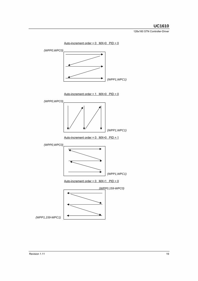
The direction of Window Program will depend on the WA (AC[0]) , PID (AC[2]), auto-increment order (AC[1]) and MX (LC[1]) register setting. WA decides whether the program RAM address advances to next row / column after reaching the specified window column / row boundary. PID controls the RAM address incrementing from WPP0 toward WPP1 (PID=0) or reverse the direction (PID=1). Auto-increment order directs the RAM address increment vertically (AC[1]=1) or horizontally (AC[1]=0). MX results the RAM column address incrementing from 127-WPC0 to 127-WPC1 (MX=1) or WPC0 to WPC1 (MX=0).
UC1610 128x160 STN Controller-Driver
Revision 1.11 19
Auto-increment order = 0 MX=0 PID = 0
(WPP0,WPC0)
(WPP1,WPC1)
Auto-increment order = 1 MX=0 PID = 0
(WPP0,WPC0)
(WPP1,WPC1)
Auto-increment order = 0 MX=0 PID = 1
(WPP0,WPC0)
(WPP1,WPC1)
Auto-increment order = 0 MX=1 PID = 0
(WPP0,159-WPC0)
(WPP1,159-WPC1)

ULTRACHIP
High-Voltage Mixed-Signal IC ©1999~2005
20 MP Specifications
Auto-increment order = 1 MX=0 PID = 1
(WPP0,WPC0)
(WPP1,WPC1)
Auto-increment order = 1 MX=1 PID = 0
(WPP0,159-WPC0)
(WPP1,159-WPC1)
Auto-increment order = 0 MX=1 PID = 1
(WPP0,159-WPC0)
(WPP1,159-WPC1)
Auto-increment order = 1 MX=1 PID = 1
(WPP0,159-WPC0)
(WPP1,159-WPC1)
UC1610 128x160 STN Controller-Driver
Revision 1.11 21
LCD VOLTAGE SETTING
MULTIPLEX RATES
Multiplex Rate is completely software programmable in UC1610 via registers CEN, DST, DEN, and partial display control LC[8:7].
Combined with low power partial display mode and a low bias ratio of 5, UC1610 can support wide variety of display control options. For example, when a system goes into stand-by mode, a large portion of LCD screen can be turned off to conserve power.
BIAS RATIO SELECTION Bias Ratio (BR) is defined as the ratio between VLCD and VBIAS, i.e. BR = VLCD /VBIAS, where VBIAS = VB1+ – VB1– = VB0+ – VB0–.
The theoretical optimum Bias Ratio can be estimated by 1+Mux . BR of value 15~20% lower/higher than the optimum value calculated above will not cause significant visible change in image quality.
Due to the nature of STN operation, an LCD designed for good gray-shade performance at high Mux Rate (e.g. MR=128), can generally perform very well as a black and white display, at lower Mux Rate. However, it is also true that such technique generally cannot maintain LCD’s quality of gray shade performance, since the contrast of the LCD will increase as the Mux Rate decreases, and the shades near the two ends of the spectrum will start to loose visibility.
UC1610 supports four BR as listed below. BR can be selected by software program.
BR 0 1 2 3 Bias Ratio 5 10 11 12
Table 1: Bias Ratios
TEMPERATURE COMPENSATION Four (4) different temperature compensation coefficients can be selected via software. The four coefficients are given below:
TC 0 1 2 3
% per oC -0.05 -0.10 -0.15 -0.20
Table 2: Temperature Compensation
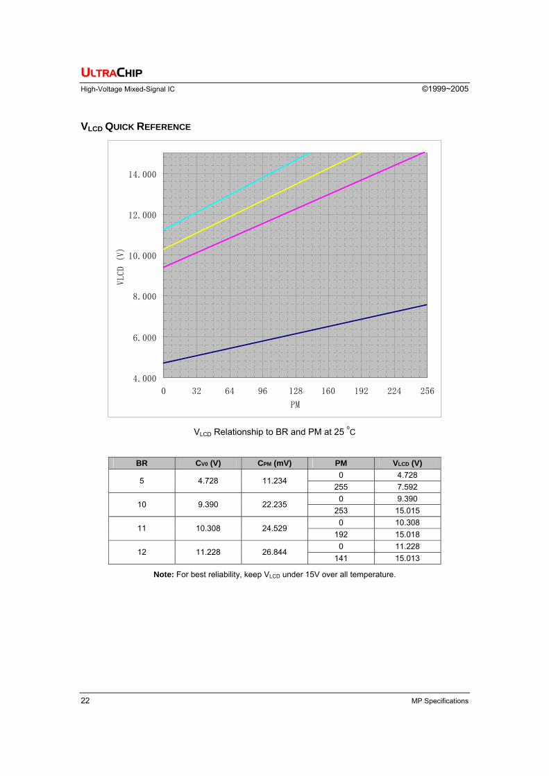
VLCD GENERATION VLCD may be supplied either by internal charge pump or by external power supply. The source of VLCD is controlled by PC[3:2]. For good product reliability, it is recommended to keep VLCD under 15V over the entire operating range.
When VLCD is generated internally, the voltage level of VLCD is determined by three control registers: BR (Bias Ratio), PM (Potentiometer), and TC (Temperature Compensation), with the following relationship:
%))25(1()( 0 TPMVLCD CTPMCCV ×−+××+=
where
CV0 and CPM are two constants, whose value depends on the setting of BR register, as illustrated in the table on the next page,
PM is the numerical value of PM register,
T is the ambient temperature in OC, and
CT is the temperature compensation coefficient as selected by TC register.
VLCD FINE TUNING Gray shade and color STN LCD is sensitive to even a 1% mismatch between IC driving voltage and the VOP of LCD. However, it is difficult for LCD makers to guarantee such high precision matching of parts from different venders. It is therefore necessary to adjust VLCD to match the actual VOP of the LCD.
For the best result, software based approach for VLCD adjustment is the recommended method for VLCD fine tuning.
For applications where mechanical manual fine tuning of VLCD becomes necessary, then VBIAS pin may be used with an external trim pot to fine tune the VLCD. Please refer to Application Notes for more detailed discussion on this subject.
LOAD DRIVING STRENGTH The power supply circuit of UC1610 is designed to handle LCD panels with load capacitance up to ~30nF when VDD2 = 2.7V. 30nF is also the recommended limit for LCD panel size for COG applications. For larger LCD panels, use higher VDD.
ULTRACHIP
High-Voltage Mixed-Signal IC ©1999~2005
22 MP Specifications
VLCD QUICK REFERENCE
4.000
6.000
8.000
10.000
12.000
14.000
0 32 64 96 128 160 192 224 256
PM
VLCD (V)
VLCD Relationship to BR and PM at 25 oC
BR CV0 (V) CPM (mV) PM VLCD (V) 0 4.728
5 4.728 11.234 255 7.592 0 9.390
10 9.390 22.235 253 15.015 0 10.308
11 10.308 24.529 192 15.018 0 11.228
12 11.228 26.844 141 15.013
Note: For best reliability, keep VLCD under 15V over all temperature.
UC1610 128x160 STN Controller-Driver
Revision 1.11 23
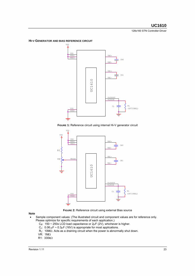
HI-V GENERATOR AND BIAS REFERENCE CIRCUIT
VB0-
VDD
CB0
VSS2
VDD
(OPTIONAL)
VLCDOUT
VB1-
VB0+VDD3
VLCDIN
UC
16
10
VB1+
VSSCL RL
VDD2
CB1
FIGURE 1: Reference circuit using internal Hi-V generator circuit
VSS2
VDD2
VLCDIN
CB1
VDD
R1
VDD
VBIAS
VB0-
VR
CB0VDD3
CL
VB0+
VB1-
(OPTIONAL)
VDD
VSS
UC
16
10
RL
VLCDOUT
VB1+
FIGURE 2: Reference circuit using external Bias source
Note • Sample component values: (The illustrated circuit and component values are for reference only.
Please optimize for specific requirements of each application.) CB: 150 ~ 250x LCD load capacitance or 2µF (2V), whichever is higher. CL: 0.06 µF ~ 0.3µF (16V) is appropriate for most applications. RL: 10MΩ. Acts as a draining circuit when the power is abnormally shut down. VR: 1MΩ R1: 330kΩ

ULTRACHIP
High-Voltage Mixed-Signal IC ©1999~2005
24 MP Specifications
LCD DISPLAY CONTROLS
CLOCK & TIMING GENERATOR UC1610 contains a built-in system clock. All required components for the clock oscillator are built-in. No external parts are required.
Four different line rates are provided for system design flexibility. The line rate is controlled by register LC[4:3]. When Mux-Rate is above 56, frame rate is calculated as:
Frame Rate = Line-Rate / Mux-Rate.
When Mux-Rate is lowered to 56 (and 24), line rate will be scaled down by 2 (and 4) times automatically to reduce power consumption.
Flicker-free frame rate is dependent on LC material and gray-shade modulation scheme. Choose lower frame rate for lower power, and choose higher frame rate to improve LCD contrast and minimize flicker.
When fast LC material with (tr + tf) < 160mS is used, faster line rate may be required under 4-shade mode to maintain good contrast ratio at operating temperature >50oC.
DRIVER MODES COM and SEG drivers can be in either Idle mode or Active mode, controlled by Display Enable flag (DC[2]). When COM drivers are in idle mode, their outputs are high-impedance (open circuit). When SEG drivers are in idle mode, their outputs are shorted to VSS.
DRIVER ARRANGEMENTS The naming conventions are: COM(x), where x=1~128, refers to the COM driver for the x-th row of pixels on the LCD panel.
The mapping of COM(x) to LCD pixel rows fixed and it is not affected by SL, CST, CEN, DST, DEN, MX or MY settings.
DISPLAY CONTROLS There are three groups of display control flags in the control register DC: Driver Enable (DE), All-Pixel-ON (APO) and Inverse (PXV). DE has the overriding effect over PXV and APO.
DRIVER ENABLE (DE)
Driver Enable is controlled by the value of DC[2] via Set Display Enable command. When DC[2] is set to OFF (logic “0”), both COM and SEG drivers will become idle and UC1610 will put itself into Sleep Mode to conserve power.
When DC[2] is set to ON, the DE flag will become “1”, and UC1610 will first exit from Sleep Mode, restore the power (VLCD, VD etc.) and then turn on COM and SEG drivers.
ALL PIXELS ON (APO)
When set, this flag will force all SEG drivers to output ON signals, disregarding the data stored in the display buffer.
This flag has no effect when Display Enable is OFF and it has no effect on data stored in RAM.
INVERSE (PXV)
When this flag is set to ON, SEG drivers will output the inverse of the value it received from the display buffer RAM (bit-wise inversion). This flag has no impact on data stored in RAM.
PARTIAL SCROLL
Control register FL specifies a region of rows which are not affected by the SL register. Since SL register can be used to implement scroll function. The FL register can be used to implement fixed region when the other part of the display is scrolled by SL.
PARTIAL DISPLAY
UC1610 provides flexible control of Mux Rate and active display area. Please refer to command description (28) ~ (30) for more detail.
GRAY-SHADE MODULATION
UC1610 uses a proprietary frame rate modulation scheme to generate 4 levels of gray shade. The relative levels of the gray shades can be programmed by setting register bit LC[6:5]. It controls the relative position of the light gray and dark gray shades. For detailed value, please refer to the register definition table.
UC1610 128x160 STN Controller-Driver
Revision 1.11 25
ITO LAYOUT CONSIDERATIONS Since the COM scanning pulses of UC1610 can be as short as 44µS, it is critical to control the RC delay of COM and SEG signal to minimize crosstalk and maintain good mass production consistency.
For COG applications, low resistance ITO glass will help reduce SEG signal RC decay, minimize VDD, VSS noise, and ensure sufficient VDD2, VSS2 supply for on-chip DC-DC converter.
ITO TRACES FOR COM SIGNALS Excessive COM scanning pulse RC decay can cause fluctuation of contrast and increase of COM direction crosstalk.
Please limit the worst case of COM signals RC delay (RCMAX) as calculated below
(RROW / 2.7 + RCOM) x CROW < 2.6µS
where
CROW: LCD loading capacitance of one row of pixels. It can be calculated by CLCD/Mux-Rate, where CLCD is the LCD panel capacitance.
RROW: ITO resistance over one row of pixels within the active area
RCOM: COM routing resistance from IC to the active area + COM driver output impedance.
(Use worst case values for all calculations)
In addition, please limit the min-max spread of RC decay to be:
| RCMAX – RCMIN | < 1µS
so that the COM distortions on the top of the screen to the bottom of the screen are uniform.
ITO TRACES FOR SEG SIGNALS Excessive SEG signal RC decay can cause image dependent changes of medium gray shades and sharply increase of SEG direction crosstalk.
To minimize crosstalk, please limit the worst case of SEG signal RC delay as calculated below.
(RCOL / 2.7 + RSEG) x CCOL < 0.35µS
where
CCOL: LCD loading capacitance of one pixel column. It can be calculated by CLCD/#_column, where CLCD is the LCD panel capacitance.
RCOL: ITO resistance over one column of pixels within the active area
RSEG: SEG routing resistance from IC to the active area + SEG driver output impedance.
(Use worst case values for all calculations)

ULTRACHIP
High-Voltage Mixed-Signal IC ©1999~2005
26 MP Specifications
RAM W/R
POL
R1
R2
R3
C1
C2
FIGURE 3: COM and SEG Driving Waveform

UC1610 128x160 STN Controller-Driver
Revision 1.11 27
HOST INTERFACE As summarized in the table below, UC1610 supports two parallel bus protocols, in either 8-bit or 4-bit bus width, and four serial bus protocols.
Designers can either use parallel bus to achieve high data transfer rate, or use serial bus to create compact LCD modules.
Bus Type 8080 6800 S8 (4wr)
S8uc (3wr)
S9 (3wr)
I2C
Width 8-bit 4-bit 8-bit 4-bit Serial Access Read/Write Write Only R/W
BM[1:0] 10 00 11 01 00 01 D[7:6] Data 00 Data 00 10 11 10 11
CS[1:0] Chip Select A[3:2] CD Control/Data –
WR0 ___ __
WR _ _ R/W 1 1 0 1
WR1 ___ __ RD EN 1 1 0 1
D[5:4] Data – Data – – Con
trol &
Dat
a P
ins
D[3:0] Data Data Data Data D0=SCK, D3=SDA * Connect unused control pins and data bus pins to VDD or VSS.
Table 3: Host interfaces Choices
ULTRACHIP
High-Voltage Mixed-Signal IC ©1999~2005
28 MP Specifications
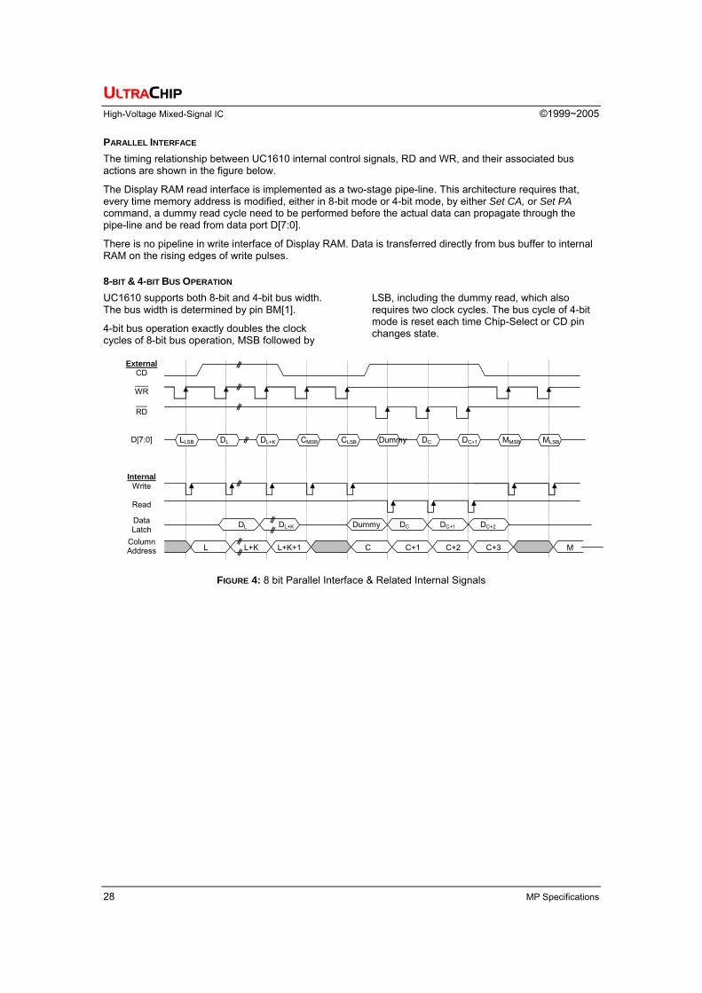
PARALLEL INTERFACE The timing relationship between UC1610 internal control signals, RD and WR, and their associated bus actions are shown in the figure below.
The Display RAM read interface is implemented as a two-stage pipe-line. This architecture requires that, every time memory address is modified, either in 8-bit mode or 4-bit mode, by either Set CA, or Set PA command, a dummy read cycle need to be performed before the actual data can propagate through the pipe-line and be read from data port D[7:0].
There is no pipeline in write interface of Display RAM. Data is transferred directly from bus buffer to internal RAM on the rising edges of write pulses.
8-BIT & 4-BIT BUS OPERATION UC1610 supports both 8-bit and 4-bit bus width. The bus width is determined by pin BM[1].
4-bit bus operation exactly doubles the clock cycles of 8-bit bus operation, MSB followed by
LSB, including the dummy read, which also requires two clock cycles. The bus cycle of 4-bit mode is reset each time Chip-Select or CD pin changes state.
LLSB DL DL+K CMSB CLSB Dummy DC DC+1 MMSB MLSB
L L+K L+K+1 C C+1 C+2 C+3 M
DL DL+K Dummy DC DC+1 DC+2
External CD ___ WR __ RD
D[7:0]
Internal Write
Read
Data Latch
Column Address
FIGURE 4: 8 bit Parallel Interface & Related Internal Signals
UC1610 128x160 STN Controller-Driver
Revision 1.11 29
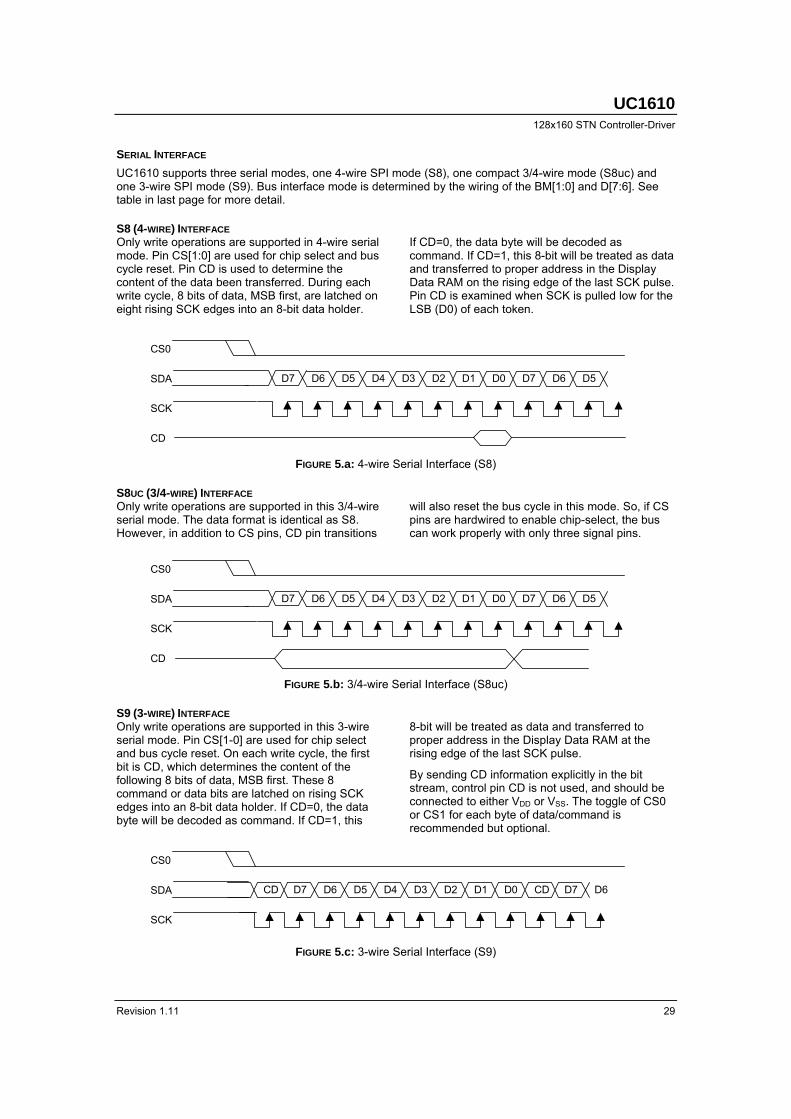
SERIAL INTERFACE UC1610 supports three serial modes, one 4-wire SPI mode (S8), one compact 3/4-wire mode (S8uc) and one 3-wire SPI mode (S9). Bus interface mode is determined by the wiring of the BM[1:0] and D[7:6]. See table in last page for more detail.
S8 (4-WIRE) INTERFACE Only write operations are supported in 4-wire serial mode. Pin CS[1:0] are used for chip select and bus cycle reset. Pin CD is used to determine the content of the data been transferred. During each write cycle, 8 bits of data, MSB first, are latched on eight rising SCK edges into an 8-bit data holder.
If CD=0, the data byte will be decoded as command. If CD=1, this 8-bit will be treated as data and transferred to proper address in the Display Data RAM on the rising edge of the last SCK pulse. Pin CD is examined when SCK is pulled low for the LSB (D0) of each token.
CS0
SDA
SCK
CD
D7 D6 D5 D4 D3 D2 D1 D0 D7 D6 D5
FIGURE 5.a: 4-wire Serial Interface (S8)
S8UC (3/4-WIRE) INTERFACE Only write operations are supported in this 3/4-wire serial mode. The data format is identical as S8. However, in addition to CS pins, CD pin transitions
will also reset the bus cycle in this mode. So, if CS pins are hardwired to enable chip-select, the bus can work properly with only three signal pins.
CS0
SDA
SCK
CD
D7 D6 D5 D4 D3 D2 D1 D0 D7 D6 D5
FIGURE 5.b: 3/4-wire Serial Interface (S8uc)
S9 (3-WIRE) INTERFACE Only write operations are supported in this 3-wire serial mode. Pin CS[1-0] are used for chip select and bus cycle reset. On each write cycle, the first bit is CD, which determines the content of the following 8 bits of data, MSB first. These 8 command or data bits are latched on rising SCK edges into an 8-bit data holder. If CD=0, the data byte will be decoded as command. If CD=1, this
8-bit will be treated as data and transferred to proper address in the Display Data RAM at the rising edge of the last SCK pulse.
By sending CD information explicitly in the bit stream, control pin CD is not used, and should be connected to either VDD or VSS. The toggle of CS0 or CS1 for each byte of data/command is recommended but optional.
CS0
SDA
SCK
CD D7 D6 D5 D4 D3 D2 D1 D0 CD D7 D6
FIGURE 5.c: 3-wire Serial Interface (S9)
ULTRACHIP
High-Voltage Mixed-Signal IC ©1999~2005
30 MP Specifications
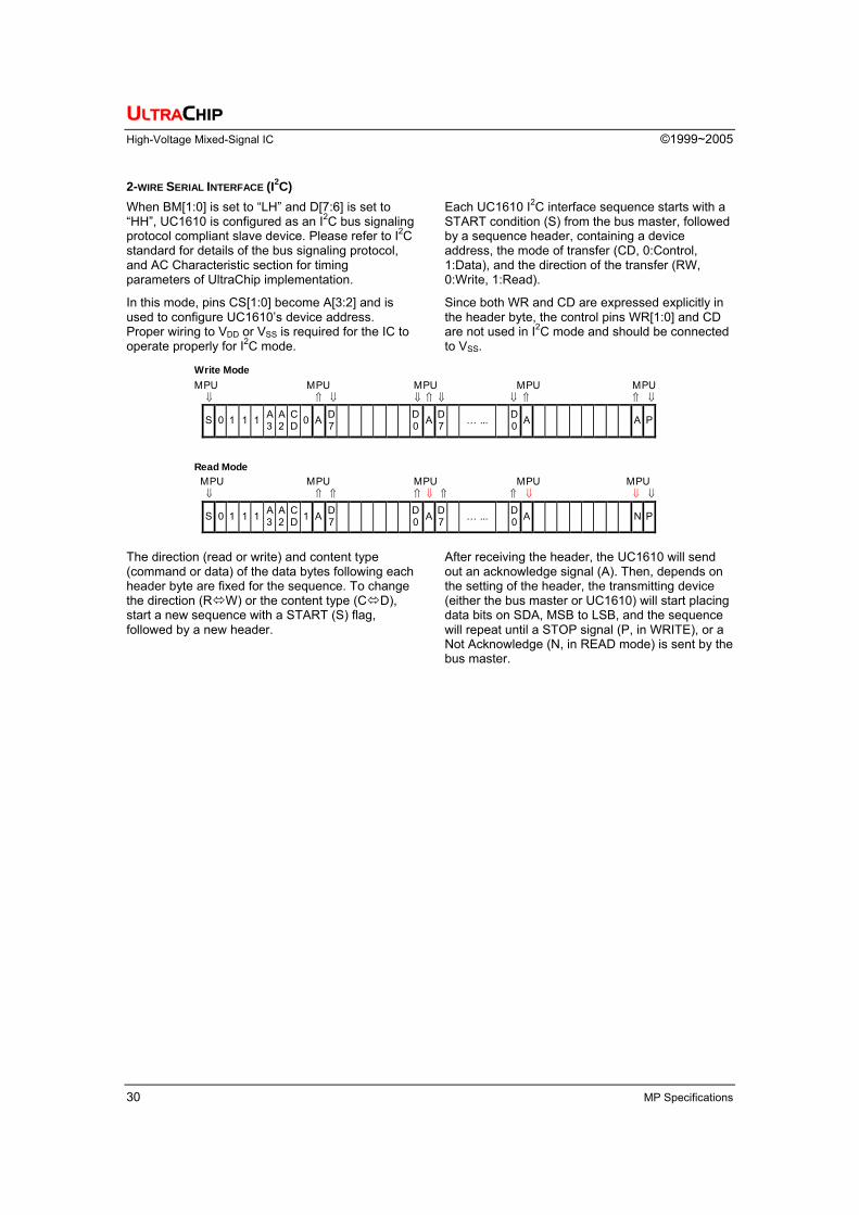
2-WIRE SERIAL INTERFACE (I2C)When BM[1:0] is set to “LH” and D[7:6] is set to “HH”, UC1610 is configured as an I2C bus signaling protocol compliant slave device. Please refer to I2C standard for details of the bus signaling protocol, and AC Characteristic section for timing parameters of UltraChip implementation.
In this mode, pins CS[1:0] become A[3:2] and is used to configure UC1610’s device address. Proper wiring to VDD or VSS is required for the IC to operate properly for I2C mode.
Each UC1610 I2C interface sequence starts with a START condition (S) from the bus master, followed by a sequence header, containing a device address, the mode of transfer (CD, 0:Control, 1:Data), and the direction of the transfer (RW, 0:Write, 1:Read).
Since both WR and CD are expressed explicitly in the header byte, the control pins WR[1:0] and CD are not used in I2C mode and should be connected to VSS.
Write Mode MPU MPU MPU MPU MPU ⇓ ⇑ ⇓ ⇓ ⇑ ⇓ ⇓ ⇑ ⇑ ⇓
S 0 1 1 1 A 3
A 2
C D 0 A D
7 D0 A D
7 … ... D0 A A P
Read Mode MPU MPU MPU MPU MPU ⇓ ⇑ ⇑ ⇑ ⇓ ⇑ ⇑ ⇓ ⇓ ⇓
S 0 1 1 1 A 3
A 2
C D 1 A D
7 D0 A D
7 … ... D0 A N P
The direction (read or write) and content type (command or data) of the data bytes following each header byte are fixed for the sequence. To change the direction (R W) or the content type (C D), start a new sequence with a START (S) flag, followed by a new header.
After receiving the header, the UC1610 will send out an acknowledge signal (A). Then, depends on the setting of the header, the transmitting device (either the bus master or UC1610) will start placing data bits on SDA, MSB to LSB, and the sequence will repeat until a STOP signal (P, in WRITE), or a Not Acknowledge (N, in READ mode) is sent by the bus master.
UC1610 128x160 STN Controller-Driver
Revision 1.11 31
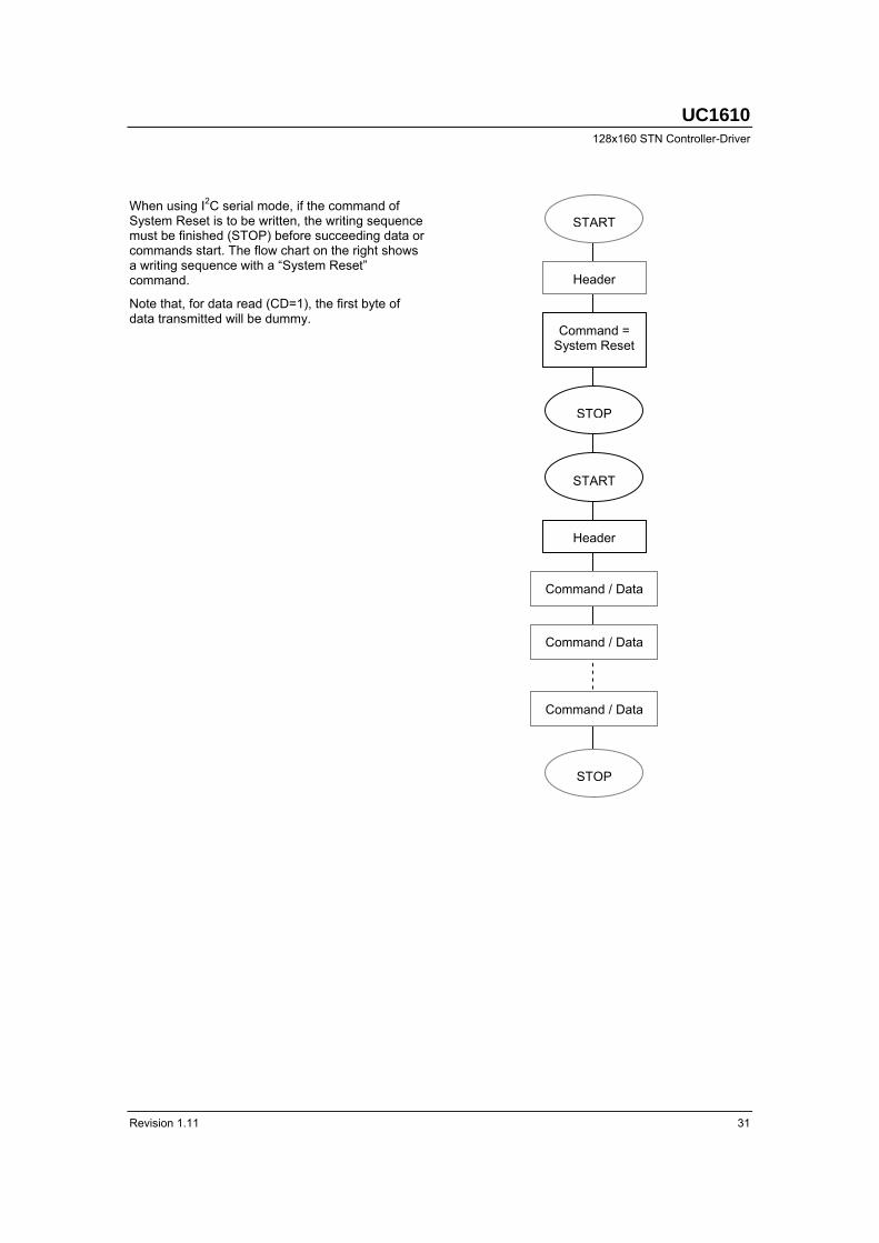
When using I2C serial mode, if the command of System Reset is to be written, the writing sequence must be finished (STOP) before succeeding data or commands start. The flow chart on the right shows a writing sequence with a “System Reset” command.
Note that, for data read (CD=1), the first byte of data transmitted will be dummy.
START
Header
STOP
START
Header
Command / Data
STOP
Command = System Reset
Command / Data
Command / Data
ULTRACHIP
High-Voltage Mixed-Signal IC ©1999~2005
32 MP Specifications
HOST INTERFACE REFERENCE CIRCUIT
MPU
WR1(RD)
CD
CS0ADDRESS UC1610
RST
VCC
VDD
CS1
WR
BM1
GND
D7-D0
VSS
VDD
VDD
ID
D7-D0
IORQ
BM0
DECODER
WR0(WR)RD
VDD
CD
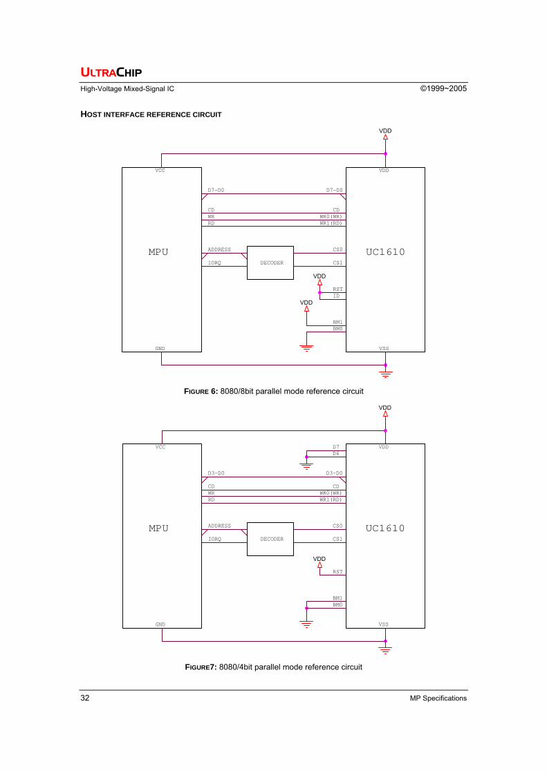
FIGURE 6: 8080/8bit parallel mode reference circuit
VDDVCC
WR1(RD)
RST
VDD
ADDRESS
DECODERIORQ
BM0
D3-D0
WR0(WR)
GND
MPUCS1
WRCD CD
D6D7
RD
CS0
D3-D0
VDD
VSS
UC1610
BM1
FIGURE7: 8080/4bit parallel mode reference circuit

UC1610 128x160 STN Controller-Driver
Revision 1.11 33
D7-D0
VSS
D7-D0
UC1610
VDD
VDD
DECODER
VDD
ADDRESS
RST
WR0(R/W)WR1(E)
BM1
VCC
ID
MPU
R/W
IORQ
CD
E
CS1
CS0
BM0
GND
VDD
CD
FIGURE 8: 6800/8bit parallel mode reference circuit
D7
VDD
CD
GND
ID
MPUDECODER
VDD
IORQ
VSS
CS1
BM0
WR0(R/W)
D3-D0
E
ADDRESS
VCC
UC1610
D3-D0
CD
VDD
BM1
CS0
D6
R/W
RSTVDD
WR1(E)
FIGURE 9: 6800/4bit parallel mode reference circuit

ULTRACHIP
High-Voltage Mixed-Signal IC ©1999~2005
34 MP Specifications
BM1
IORQ
SCK(D0)
CS0
VDD
SDA
WR0
DECODER
WR1
GND
BM0
VSS
VDD
CS1
CD
UC1610ADDRESS
D7
RST
MPU
CD
VDDD6
VCC
SDA(D3)
ID
SCK
FIGURE 10: 4-Wires SPI (S8) serial mode reference circuit
VCC
GND
BM1
MPU
CS1
SCK
VDD
RST
UC1610
D7
VSS
CS0
CD
VDD
VDD
ID
SDA(D3)
BM0
SDASCK(D0)
WR0
VDD
CD
WR1
D6
FIGURE 11: 3/4-Wires SPI (S8uc) serial mode reference circuit
UC1610 128x160 STN Controller-Driver
Revision 1.11 35
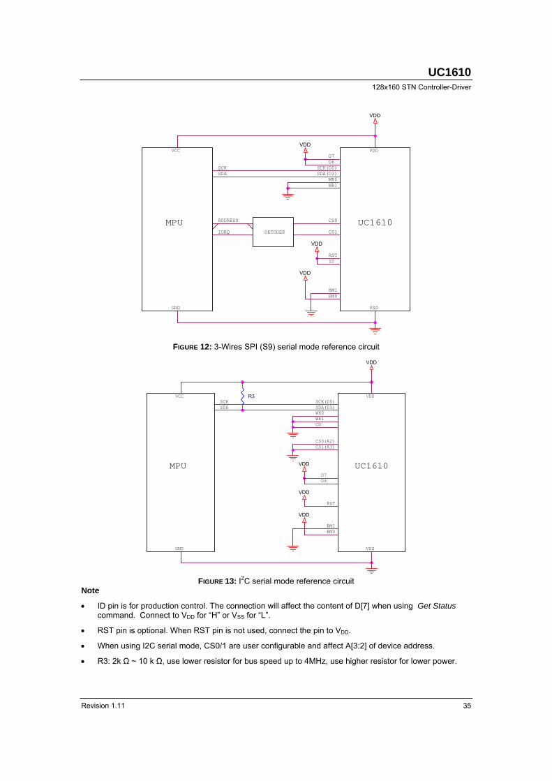
VDD
CS0
VSSGND
D6
ID
VDD
SDA
IORQ
VDD
RST
WR0
MPU
SDA(D3)
WR1
VDDD7
BM1
CS1DECODER
BM0
ADDRESS
SCK
VCC
SCK(D0)
UC1610
VDD
FIGURE 12: 3-Wires SPI (S9) serial mode reference circuit
BM0
VDD
UC1610
WR0
BM1
CS0(A2)
VDD
CD
D6
SDA
GND
D7
R3
SDA(D3)
VDD
RST
VSS
SCK
WR1
VDD
VDD
MPU
SCK(D0)
CS1(A3)
VCC
FIGURE 13: I2C serial mode reference circuit
Note
• ID pin is for production control. The connection will affect the content of D[7] when using Get Status command. Connect to VDD for “H” or VSS for “L”.
• RST pin is optional. When RST pin is not used, connect the pin to VDD.
• When using I2C serial mode, CS0/1 are user configurable and affect A[3:2] of device address.
• R3: 2k Ω ~ 10 k Ω, use lower resistor for bus speed up to 4MHz, use higher resistor for lower power.
ULTRACHIP
High-Voltage Mixed-Signal IC ©1999~2005
36 MP Specifications
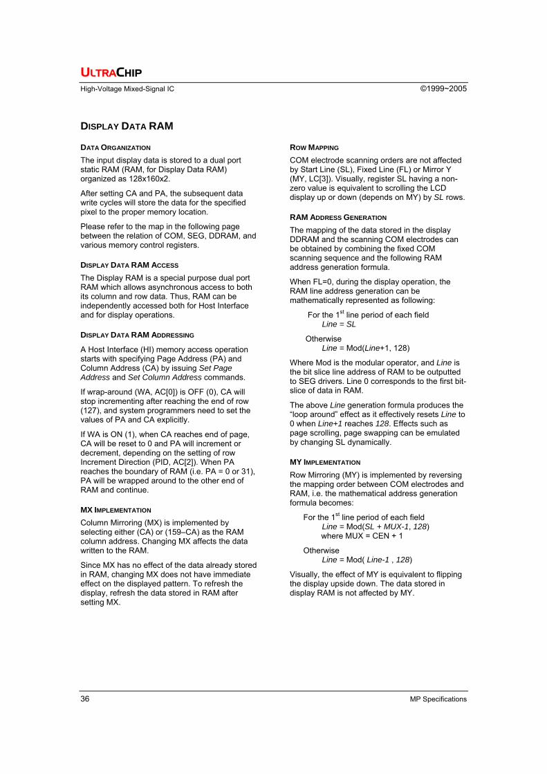
DISPLAY DATA RAM
DATA ORGANIZATION The input display data is stored to a dual port static RAM (RAM, for Display Data RAM) organized as 128x160x2.
After setting CA and PA, the subsequent data write cycles will store the data for the specified pixel to the proper memory location.
Please refer to the map in the following page between the relation of COM, SEG, DDRAM, and various memory control registers.
DISPLAY DATA RAM ACCESS The Display RAM is a special purpose dual port RAM which allows asynchronous access to both its column and row data. Thus, RAM can be independently accessed both for Host Interface and for display operations.
DISPLAY DATA RAM ADDRESSING
A Host Interface (HI) memory access operation starts with specifying Page Address (PA) and Column Address (CA) by issuing Set Page Address and Set Column Address commands.
If wrap-around (WA, AC[0]) is OFF (0), CA will stop incrementing after reaching the end of row (127), and system programmers need to set the values of PA and CA explicitly.
If WA is ON (1), when CA reaches end of page, CA will be reset to 0 and PA will increment or decrement, depending on the setting of row Increment Direction (PID, AC[2]). When PA reaches the boundary of RAM (i.e. PA = 0 or 31), PA will be wrapped around to the other end of RAM and continue.
MX IMPLEMENTATION Column Mirroring (MX) is implemented by selecting either (CA) or (159–CA) as the RAM column address. Changing MX affects the data written to the RAM.
Since MX has no effect of the data already stored in RAM, changing MX does not have immediate effect on the displayed pattern. To refresh the display, refresh the data stored in RAM after setting MX.
ROW MAPPING COM electrode scanning orders are not affected by Start Line (SL), Fixed Line (FL) or Mirror Y (MY, LC[3]). Visually, register SL having a non-zero value is equivalent to scrolling the LCD display up or down (depends on MY) by SL rows.
RAM ADDRESS GENERATION The mapping of the data stored in the display DDRAM and the scanning COM electrodes can be obtained by combining the fixed COM scanning sequence and the following RAM address generation formula.
When FL=0, during the display operation, the RAM line address generation can be mathematically represented as following:
For the 1st line period of each field Line = SL
Otherwise Line = Mod(Line+1, 128)
Where Mod is the modular operator, and Line is the bit slice line address of RAM to be outputted to SEG drivers. Line 0 corresponds to the first bit-slice of data in RAM.
The above Line generation formula produces the “loop around” effect as it effectively resets Line to 0 when Line+1 reaches 128. Effects such as page scrolling, page swapping can be emulated by changing SL dynamically.
MY IMPLEMENTATION Row Mirroring (MY) is implemented by reversing the mapping order between COM electrodes and RAM, i.e. the mathematical address generation formula becomes:
For the 1st line period of each field Line = Mod(SL + MUX-1, 128)
where MUX = CEN + 1
Otherwise Line = Mod( Line-1 , 128)
Visually, the effect of MY is equivalent to flipping the display upside down. The data stored in display RAM is not affected by MY.

UC1610 128x160 STN Controller-Driver
Revision 1.11 37
WINDOW PROGRAM Window program is designed for data write in a specified window range of DDRAM address. The procedure should start with window boundary registers setting (WPP0, WPP1, WPC0 and WPC1) and then enable AC[4]. After AC[4] sets, data can be written to DDRAM within the window address range which is specified by (WPP0, WPC0) and (WPP1, WPC1). AC[4] should be cleared after any modification of window boundary registers and then set again in order to initialize another window program.
The data write direction will be determined by AC[2:0] and MX settings. When AC[0]=1, the data write can be consecutive within the range of the specified window. AC[1] will control the data write in either column or row direction. AC[2] will result the data write starting either from row WPP0 or WPP1. MX is for the initial column address either from WPC0 to WPC1 or from (MC-WPC0 to MC-WPC1).
Example1: Example 2:
AC[2:0] = 001 MX=0 AC[2:0] = 111 MX = 0
column
0 159
row
31
(WPP0, WPC0)
(WPP1,WPC1)
(WPP0, WPC0)
(WPP1,WPC1)
ULTRACHIP
High-Voltage Mixed-Signal IC ©1999~2005
38 MP Specifications
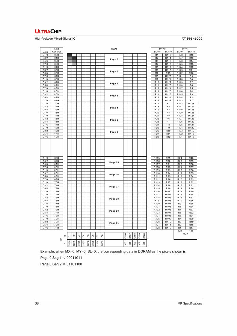
Line RAMAdderss SL=0 SL=16 SL=0 SL=16
D1/0 00H R1 R113 R128 R16D3/2 01H R2 R114 R127 R15D5/4 02H R3 R115 R126 R14D7/6 03H R4 R116 R125 R13D1/0 04H R5 R117 R124 R12D3/2 05H R6 R118 R123 R11D5/4 06H R7 R19 R122 R10D7/6 07H R8 R120 R121 R9D1/0 08H R9 R121 R120 R8D3/2 09H R10 R122 R119 R7D5/4 0AH R11 R123 R118 R6D7/6 0BH R12 R124 R117 R5D1/0 0CH R13 R125 R116 R4D3/2 0DH R14 R126 R115 R3D5/4 0EH R15 R127 R114 R2D7/6 0FH R16 R128 R113 R1D1/0 10H R17 R1 R112 R128D3/2 11H R18 R2 R111 R127D5/4 12H R19 R3 R110 R126D7/6 13H R20 R4 R109 R125D1/0 14H R21 R5 R108 R124D3/2 15H R22 R6 R107 R123D5/4 16H R23 R7 R106 R122D7/6 17H R24 R8 R105 R121D1/0 18H R25 R9 R104 R120D3/2 19H R26 R10 R103 R119D5/4 1AH R27 R11 R102 R118D7/6 1BH R28 R12 R101 R117
D1/0 68H R105 R89 R24 R40D3/2 69H R106 R90 R23 R39D5/4 6AH R107 R91 R22 R38D7/6 6BH R108 R93 R21 R37D1/0 6CH R109 R93 R20 R36D3/2 6DH R110 R94 R19 R35D5/4 6EH R111 R95 R18 R34D7/6 6FH R112 R96 R17 R33D1/0 70H R113 R97 R16 R32D3/2 71H R114 R98 R15 R31D5/4 72H R115 R99 R14 R30D7/6 73H R116 R100 R13 R29D1/0 74H R117 R101 R12 R28D3/2 75H R118 R102 R11 R27D5/4 76H R19 R103 R10 R26D7/6 77H R120 R104 R9 R25D1/0 78H R121 R105 R8 R24D3/2 79H R122 R106 R7 R23D5/4 7AH R123 R107 R6 R22D7/6 7BH R124 R108 R5 R21D1/0 7CH R125 R109 R4 R20D3/2 7DH R126 R110 R3 R19D5/4 7EH R127 R111 R2 R18D7/6 7FH R128 R112 R1 R17
128 128
0 C1
C2
C3
C4
C5
C6
C7
C8
C15
6
C15
7
C15
8
C15
9
C16
0
1
C16
0
C15
9
C15
8
C15
7
C15
6
C15
5
C15
4
C15
3
C5
C4
C3
C2
C1
MY=0
Page 6
MX
Page 2
Page 3
Page 4
Page 5
Page 0
Page 1
Data
MUX
Page 25
Page 26
Page 27
Page 28
Page 30
Page 31
MY=1
Example: when MX=0, MY=0, SL=0, the corresponding data in DDRAM as the pixels shown is:
Page 0 Seg 1 00011011
Page 0 Seg 2 01101100

UC1610 128x160 STN Controller-Driver
Revision 1.11 39
RESET & POWER MANAGEMENT
TYPES OF RESET UC1610 has two different types of Reset: Power-ON-Reset and System-Reset.
Power-ON-Reset is performed right after VDD is connected to power. Power-On-Reset will first wait for about ~5mS, depending on the time required for VDD to stabilize, and then trigger the System Reset.
System Reset can also be activated by software command or by connecting RST pin to ground.
In the following discussions, Reset means System Reset.
RESET STATUS When UC1610 enters RESET sequence:
• Operation mode will be “Reset”
• System Status bits RS and BZ will stay as “1” until the Reset process is completed. When RS=1, the IC will only respond to Read Status command. All other commands are ignored.
• All control registers are reset to default values. Refer to Control Registers for details of their default values.
OPERATION MODES UC1610 has three operating modes (OM): Reset, Normal, Sleep.
Mode Reset Sleep NormalOM 00 10 11
Host Interface Active Active ActiveClock OFF OFF ON
LCD Drivers OFF OFF ON Charge Pump OFF OFF ON
Draining Circuit ON ON OFF
Table 4: Operating Modes
CHANGING OPERATION MODE In addition to Power-ON-Reset, two commands will initiate OM transitions:
Set Display Enable, and System Reset.
When DC[2] is modified by Set Display Enable, OM will be updated automatically. There is no other action required to enter Sleep Mode.
OM changes are synchronized with the edges of UC1610 internal clock. To ensure consistent system states, wait at least 10µS after Set Display Enable or System Reset command.
Action Mode OM Reset command
RST_ pin pulled “L” Power ON reset
Reset 00
Set Driver Enable to “0” Sleep 10 Set Driver Enable to “1” Normal 11
Table 5: OM changes
Both Reset mode and Sleep mode drain the charges stored in the external capacitors CB0, CB1, and CL. When entering Reset mode or Sleep mode, the display drivers will be disabled.
The difference between Sleep mode and Reset mode is that, Reset mode clears all control registers and restores them to default values, while Sleep mode retains all the control registers values set by the user.
It is recommended to use Sleep Mode for Display OFF operations as UC1610 consumes very little energy in Sleep mode (typically under 2µA).
EXITING SLEEP MODE UC1610 contains internal logic to check whether VLCD and VBIAS are ready before releasing COM and SEG drivers from their idle states. When exiting Sleep or Reset mode, COM and SEG drivers will not be activated until UC1610 internal voltage sources are restored to their proper values.
ULTRACHIP
High-Voltage Mixed-Signal IC ©1999~2005
40 MP Specifications
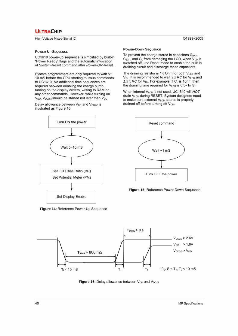
POWER-UP SEQUENCE UC1610 power-up sequence is simplified by built-in “Power Ready” flags and the automatic invocation of System-Reset command after Power-ON-Reset.
System programmers are only required to wait 5~ 10 mS before the CPU starting to issue commands to UC1610. No additional time sequences are required between enabling the charge pump, turning on the display drivers, writing to RAM or any other commands. However, while turning on VDD, VDD2/3 should be started not later than VDD.
Delay allowance between VDD and VDD2/3 is illustrated as Figure 16.
POWER-DOWN SEQUENCE To prevent the charge stored in capacitors CBX+, CBX–, and CL from damaging the LCD, when VDD is switched off, use Reset mode to enable the built-in draining circuit and discharge these capacitors.
The draining resistor is 1K Ohm for both VLCD and VB+. It is recommended to wait 3 x RC for VLCD and 1.5 x RC for VB+. For example, if CL is 10nF, then the draining time required for VLCD is 0.5~1mS.
When internal VLCD is not used, UC1610 will NOT drain VLCD during RESET. System designers need to make sure external VLCD source is properly drained off before turning off VDD.
Figure 14: Reference Power-Up Sequence
Figure 15: Reference Power-Down Sequence
Figure 16: Delay allowance between VDD and VDD23
TDelay > 0 s
VDD2/3 > 2.6V
VDD > 1.8V
VDD2/3 > VDD
10μS < T1, T2 < 10 mS T1 T2
TWait > 800 mS
Tf < 10 mS
Turn ON the power
Set LCD Bias Ratio (BR)
Set Potential Meter (PM)
Set Display Enable
Wait 5~10 mS
Turn OFF the power
Reset command
Wait ~1 mS
UC1610 128x160 STN Controller-Driver
Revision 1.11 41
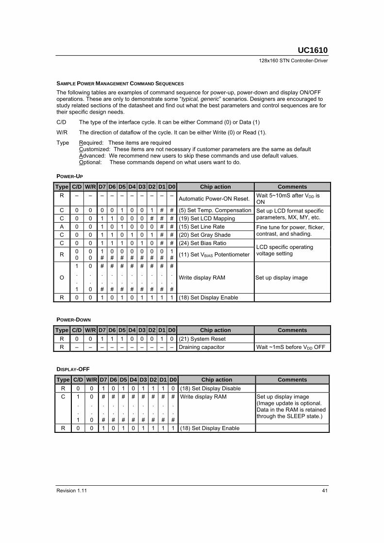
SAMPLE POWER MANAGEMENT COMMAND SEQUENCES The following tables are examples of command sequence for power-up, power-down and display ON/OFF operations. These are only to demonstrate some “typical, generic” scenarios. Designers are encouraged to study related sections of the datasheet and find out what the best parameters and control sequences are for their specific design needs.
C/D The type of the interface cycle. It can be either Command (0) or Data (1)
W/R The direction of dataflow of the cycle. It can be either Write (0) or Read (1).
Type Required: These items are required Customized: These items are not necessary if customer parameters are the same as default Advanced: We recommend new users to skip these commands and use default values. Optional: These commands depend on what users want to do.
POWER-UP
Type C/D W/R D7 D6 D5 D4 D3 D2 D1 D0 Chip action Comments R – – – – – – – – – – Automatic Power-ON Reset. Wait 5~10mS after VDD is
ON C 0 0 0 0 1 0 0 1 # # (5) Set Temp. CompensationC 0 0 1 1 0 0 0 # # # (19) Set LCD Mapping
Set up LCD format specific parameters, MX, MY, etc.
A 0 0 1 0 1 0 0 0 # # (15) Set Line Rate C 0 0 1 1 0 1 0 1 # # (20) Set Gray Shade
Fine tune for power, flicker, contrast, and shading.
C 0 0 1 1 1 0 1 0 # # (24) Set Bias Ratio
R 0 0
0 0
1 #
0#
0 #
0 #
0 #
0 #
0#
1# (11) Set VBIAS Potentiometer
LCD specific operating voltage setting
O
1 . . 1
0 . . 0
# . . #
#..#
# . . #
# . . #
# . . #
# . . #
#..#
#..#
Write display RAM Set up display image
R 0 0 1 0 1 0 1 1 1 1 (18) Set Display Enable
POWER-DOWN
Type C/D W/R D7 D6 D5 D4 D3 D2 D1 D0 Chip action Comments R 0 0 1 1 1 0 0 0 1 0 (21) System Reset R – – – – – – – – – – Draining capacitor Wait ~1mS before VDD OFF
DISPLAY-OFF
Type C/D W/R D7 D6 D5 D4 D3 D2 D1 D0 Chip action Comments R 0 0 1 0 1 0 1 1 1 0 (18) Set Display Disable C 1
.
. 1
0 . . 0
# . . #
#..#
# . . #
# . . #
# . . #
# . . #
#..#
#..#
Write display RAM Set up display image (Image update is optional. Data in the RAM is retained through the SLEEP state.)
R 0 0 1 0 1 0 1 1 1 1 (18) Set Display Enable
ULTRACHIP
High-Voltage Mixed-Signal IC ©1999~2005
42 MP Specifications
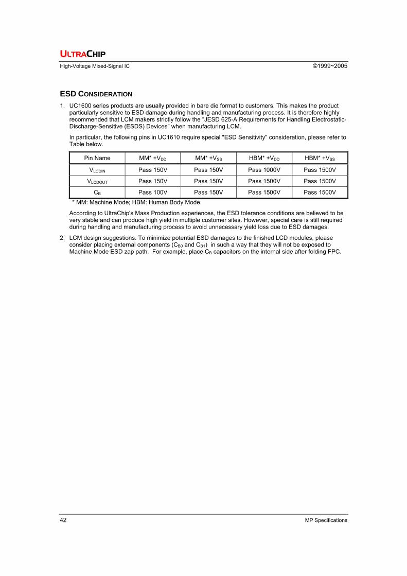
ESD CONSIDERATION 1. UC1600 series products are usually provided in bare die format to customers. This makes the product
particularly sensitive to ESD damage during handling and manufacturing process. It is therefore highly recommended that LCM makers strictly follow the "JESD 625-A Requirements for Handling Electrostatic-Discharge-Sensitive (ESDS) Devices" when manufacturing LCM.
In particular, the following pins in UC1610 require special "ESD Sensitivity" consideration, please refer to Table below.
Pin Name MM* +VDD MM* +VSS HBM* +VDD HBM* +VSS
VLCDIN Pass 150V Pass 150V Pass 1000V Pass 1500V
VLCDOUT Pass 150V Pass 150V Pass 1500V Pass 1500V
CB Pass 100V Pass 150V Pass 1500V Pass 1500V * MM: Machine Mode; HBM: Human Body Mode
According to UltraChip's Mass Production experiences, the ESD tolerance conditions are believed to be very stable and can produce high yield in multiple customer sites. However, special care is still required during handling and manufacturing process to avoid unnecessary yield loss due to ESD damages.
2. LCM design suggestions: To minimize potential ESD damages to the finished LCD modules, please consider placing external components (CB0 and CB1) in such a way that they will not be exposed to Machine Mode ESD zap path. For example, place CB capacitors on the internal side after folding FPC.

UC1610 128x160 STN Controller-Driver
Revision 1.11 43
ABSOLUTE MAXIMUM RATINGS In accordance with IEC134, note 1 and 2
Symbol Parameter Min. Max. UnitVDD Logic Supply voltage -0.3 +4.0 V
VDD2 LCD Generator Supply voltage -0.3 +4.0 V
VDD3 Analog Circuit Supply voltage -0.3 +4.0 V
VDD2/3-VDD Voltage difference between VDD and VDD2/3 -- 1.6 V
VLCD LCD Generated voltage (-30OC ~ +80OC) -0.3 +18.0 V
VIN Digital input signal -0.4 VDD + 0.5 V
TOPR Operating temperature range -30 +85 oC
TSTR Storage temperature -55 +125 oC
Notes 1. VDD is based on VSS = 0V
2. Stress beyond ranges listed above may cause permanent damages to the device.
ULTRACHIP
High-Voltage Mixed-Signal IC ©1999~2005
44 MP Specifications
SPECIFICATIONS
DC CHARACTERISTICS
Symbol Parameter Conditions Min. Typ. Max. UnitVDD Supply for digital circuit 1.8 3.3 V
VDD2/3 Supply for bias & pump 2.6 3.3 V
VLCD Charge pump output VDD2/3 2.6V, 25OC 13.5 15 V
VD LCD data voltage VDD2/3 2.6V, 25OC 0.9 1.5 V
VIL Input logic LOW 0.2VDD V
VIL(Serial) Input logic LOW in serial Mode 0.15VDD
VIH Input logic HIGH 0.8VDD V
VIH(Serial) Input logic HIGH in serial Mode 0.85VDD
VOL Output logic LOW 0.2VDD V
VOH Output logic HIGH 0.8VDD V
IIL Input leakage current 1.5 µA
CIN Input capacitance 5 10 pF
COUT Output capacitance 5 10 pF
R0N(SEG) SEG output impedance VLCD = 14.7V 1.2 2.5 kΩ
R0N(COM) COM output impedance VLCD = 14.7V 2.0 4.0 kΩ
fLINE Average Line rate LC[4:3] = 11b 11.1 12.1 - kHz
POWER CONSUMPTION
VDD =2.7, Bias Ratio =10b, PM = 178, Line Rate = 00b, PL =16~21nF, MR = 128, Bus mode = 6800, CL = 0.3µF, CB = 2µF, CBIAS = 0.1µF. All outputs are open circuit.
Display Pattern Conditions Typ. (µA) Max. (µA) All-OFF Bus = idle 617 925
2-pixel checker Bus = idle 725 1087 - Bus = idle (standby current) - 5
UC1610 128x160 STN Controller-Driver
Revision 1.11 45
AC CHARACTERISTICS
FIGURE 17: Parallel Bus Timing Characteristics (for 8080 MCU)
(2.5V VDD < 3.3V, Ta= –30 to +85oC)
Symbol Signal Description Condition Min. Max. UnitstAS80 tAH80
CD Address setup time Address hold time
5 15
– nS
tCY80 System cycle time 8 bits bus (read) (write) 4 bits bus (read) (write)
140 80 140 80
– nS
tPWR80 WR1 Pulse width 8 bits (read) 4 bits
70 70
– nS
tPWW80 WR0 Pulse width 8 bits (write) 4 bits
40 40
– nS
tHPW80 WR0, WR1 High pulse width 8 bits bus (read) (write) 4 bits bus (read) (write)
70 40 70 40
– nS
tDS80 tDH80
D0~D7 Data setup time Data hold time
30 15
– nS
tACC80 tOD80
Read access time Output disable time
CL = 100pF – 25
60
nS
tCSSA80
tCSH80 CS1/CS0 Chip select setup time 5
5 nS
CD tAS80 tAH80 CS0 CS1 tCSSA80 tCY80 tCSH80 tPWR80, tPWW80 tHPW80 WR0 WR1
tDS80 tDH80
Write D[7:0] tACC80 tOD80 Read D[7:0]
ULTRACHIP
High-Voltage Mixed-Signal IC ©1999~2005
46 MP Specifications
(1.8V VDD < 2.5V, Ta= –30 to +85oC)
Symbol Signal Description Condition Min. Max. UnitstAS80 tAH80 CD
Address setup time Address hold time
10 30
– nS
tCY80
System cycle time 8 bits bus (read) (write) 4 bits bus (read) (write)
280 160 280 160
– nS
tPWR80 WR1 Pulse width 8 bits (read) 4 bits (read)
140 140
– nS
tPWW80 WR0 Pulse width 8 bits (write) 4 bits (write)
80 80
– nS
tHPW80
WR0, WR1
High pulse width 8 bits bus (read) (write) 4 bits bus (read) (write)
140 80 140 80
– nS
tDS80 tDH80 D0~D7
Data setup time Data hold time
60 30
– nS
tACC80 tOD80
Read access time Output disable time
CL = 100pF - 50
nS
tCSSA80
tCSH80 CS1/CS0 Chip select setup time 10
10 nS
UC1610 128x160 STN Controller-Driver
Revision 1.11 47
FIGURE 18: Parallel Bus Timing Characteristics (for 6800 MCU)
(2.5V VDD < 3.3V, Ta= –30 to +85oC)
Symbol Signal Description Condition Min. Max. UnitstAS68 tAH68
CD Address setup time Address hold time
5 15
– nS
tCY68 System cycle time 8 bits bus (read) (write) 4 bits bus (read) (write)
140 80 140 80
– nS
tPWR68 WR1 Pulse width 8 bits (read) 4 bits
70 70
– nS
tPWW68 Pulse width 8 bits (write) 4 bits
40 40
– nS
tLPW68 Low pulse width 8 bits bus (read) (write) 4 bits bus (read) (write)
70 40 70 40
– nS
tDS68 tDH68
D0~D7 Data setup time Data hold time
30 15
– nS
tACC68 tOD68
Read access time Output disable time
CL = 100pF – 25
60
nS
tCSSA68
tCSH68 CS1/CS0 Chip select setup time 5
5 nS
CD tAS68 tAH68 CS0 CS1 tCSSA68 tCY68 tCSH68 tPWR68, tPWW68 tLPW68 WR1
tDS68 tDH68
Write D[7:0] tACC68 tOD68 Read D[7:0]

ULTRACHIP
High-Voltage Mixed-Signal IC ©1999~2005
48 MP Specifications
(1.8V VDD < 2.5V, Ta= –30 to +85oC)
Symbol Signal Description Condition Min. Max. UnitstAS68 tAH68
CD Address setup time Address hold time
10 30
– nS
tCY68 System cycle time 8 bits bus (read) (write) 4 bits bus (read) (write)
280 160 280 160
– nS
tPWR68 WR1 Pulse width 8 bits (read) 4 bits
140 140
– nS
tPWW68 Pulse width 8 bits (write) 4 bits
80 80
– nS
tLPW68 Low pulse width 8 bits bus (read) (write) 4 bits bus (read) (write)
140 80 140 80
– nS
tDS68 tDH68
D0~D7 Data setup time Data hold time
60 30
– nS
tACC68 tOD68
Read access time Output disable time
CL = 100pF - 50
nS
TCSSA68
TCSH68 CS1/CS0 Chip select setup time 10
10 nS

UC1610 128x160 STN Controller-Driver
Revision 1.11 49
FIGURE 19: Serial Bus Timing Characteristics (for S8 / S8uc)
(2.5V VDD < 3.3V, Ta= –30 to +85oC)
Symbol Signal Description Condition Min. Max. UnitstASS8 Address setup time 5 – nS tAHS8
CD Address hold time 20 – nS
tCYS8 System cycle time 125 – nS tLPWS8 Low pulse width 60 – nS tHPWS8
SCK High pulse width 60 – nS
tDSS8 tDHS8
SDA Data setup time Data hold time
30 20
– nS
tCSSAS8
tCSHS8 CS1/CS0 Chip select setup time 5
15 nS
(1.8V VDD < 2.5V, Ta= –30 to +85oC)
Symbol Signal Description Condition Min. Max. UnitstASS8 Address setup time 10 – nS tAHS8
CD Address hold time 45 – nS
tCYS8 System cycle time 250 – nS tLPWS8 Low pulse width 120 – nS tHPWS8
SCK High pulse width 120 – nS
tDSS8 tDHS8
SDA Data setup time Data hold time
60 40
– nS
tCSSAS8
tCSHS8 CS1/CS0 Chip select setup time 10
30 nS
CD tASS8 tAHS8 CS0 CS1 tCSSAS8 tCYS8 tCSHS8 tLPWS8 tHPWS8 SCK
tDSS8 tDHS8
SDA

ULTRACHIP
High-Voltage Mixed-Signal IC ©1999~2005
50 MP Specifications
FIGURE 20: Serial Bus Timing Characteristics (for S9)
(2.5V VDD < 3.3V, Ta= –30 to +85oC)
Symbol Signal Description Condition Min. Max. UnitstCYS9 System cycle time 80 – nS tLPWS9 Low pulse width 35 – nS tHPWS9
SCK High pulse width 35 – nS
tDSS9 tDHS9
SDA Data setup time Data hold time
30 20
– nS
tCSSAS9
tCSHS9 CS1/CS0 Chip select setup time 5
5 nS
(1.8V VDD < 2.5V, Ta= –30 to +85oC)
Symbol Signal Description Condition Min. Max. UnitstCYS9 System cycle time 160 – nS tLPWS9 Low pulse width 70 – nS tHPWS9
SCK High pulse width 70 – nS
tDSS9 tDHS9
SDA Data setup time Data hold time
60 40
– nS
tCSSAS9
tCSHS9 CS1/CS0 Chip select setup time 10
10 nS
CS0 CS1 tCSS9 tCYS9 tCSHS9 tWLS9 tWHS9 SCK
tDSS9 tDHS9
SDA

UC1610 128x160 STN Controller-Driver
Revision 1.11 51
FIGURE 21: Serial bus timing characteristics (for I2C)
(2.5V VDD < 3.3V, Ta= –30 to +85oC)
Symbol Signal Description Condition Min. Max. UnitstCYI2C SCK cycle time tr+tf 100nS 250 – nS tLPWI2C Low pulse width 65 – nS tHPWI2C
SCK High pulse width 65 – nS
tr, tf Rise time and fall time – – nS tSSDAI2C Data setup time 25 – nS tHDAI2C Data hold time 10 – nS tSSTAI2C START Setup time 25 – nS tHSTAI2C STAR Hold time 20 – nS tSSTOI2C
SCK SDA
STOP setup time 25 – nS
(1.8V VDD < 2.5V, Ta= –30 to +85oC)
Symbol Signal Description Condition Min. Max. UnitstCYI2C SCK cycle time tr+tf 100ns 300 – nS tLPWI2C Low pulse width 100 – nS tHPWI2C
SCK High pulse width 100 – nS
tr, tf Rise time and fall time – – nS tSSDAI2C Data setup time 40 – nS tHDAI2C Data hold time 10 – nS tSSTAI2C START Setup time 25 – nS tHSTAI2C STAR Hold time 35 – nS tSSTOI2C
SCK SDA
STOP setup time 25 – nS
S tHPWI2C tLPWI2C
SCK
tSSTAI2C tHSTAI2C tSDATI2C tHDATI2C tSSTOI2C
tBUF tCYI2C
SDA
P
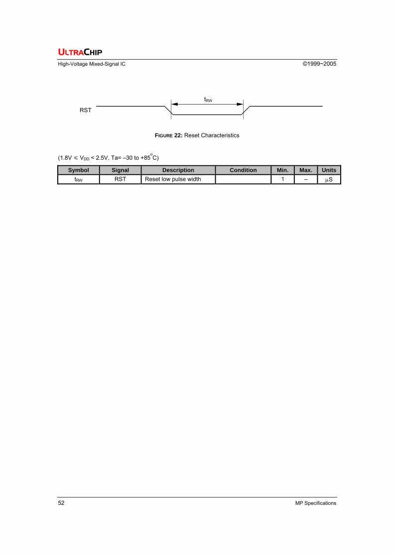
ULTRACHIP
High-Voltage Mixed-Signal IC ©1999~2005
52 MP Specifications
RST
tRW
FIGURE 22: Reset Characteristics
(1.8V VDD < 2.5V, Ta= –30 to +85oC)
Symbol Signal Description Condition Min. Max. UnitstRW RST Reset low pulse width 1 – µS
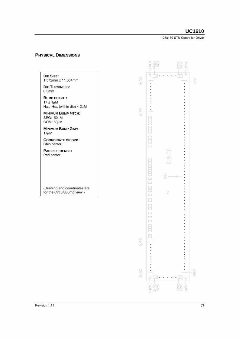
UC1610 128x160 STN Controller-Driver
Revision 1.11 53
PHYSICAL DIMENSIONS
DIE SIZE: 1.372mm x 11.384mm
DIE THICKNESS: 0.5mm
BUMP HEIGHT: 17 ± 1µM HMax-HMin (within die) < 2µM
MINIMUM BUMP PITCH: SEG: 50µM COM: 50µM
MINIMUM BUMP GAP: 17µM
COORDINATE ORIGIN: Chip center
PAD REFERENCE: Pad center
(Drawing and coordinates are for the Circuit/Bump view.)

ULTRACHIP
High-Voltage Mixed-Signal IC ©1999~2005
54 MP Specifications
ALIGNMENT MARK INFORMATION
COORDINATES:
U-Left Mark U-Right Mark X Y X Y
1 -5496.3 623.8 5430.4 625.9 2 -5480.7 591.9 5497.8 578.6 3 -5449.5 576.4 5452.1 625.9
D-Left Mark D-Right Mark
X Y X Y 1 -5474.3 -591.0 5467.9 -591.0 2 -5463.3 -646.0 5478.9 -646.0 3 -5496.3 -613.0 5445.9 -613.0 4 -5441.3 -624.0 5501.0 -624.0 C -5468.8 -618.5 5473.4 -618.5
(The values of the x-coordinate and the y-coordinate in the table are after rounded.)
FOR NON-OTP PROCESS CROSS-SECTION
Metal3 / 9KÅ
SiO2 / 5KÅ
SiN / 7KÅ
SHAPE OF THE ALIGNMENT MARK:
(0,0)
D-Left Mark
D-Right Mark
U-Left Mark
U-Right Mark
3 2
1
2
1
2
3 1
3
4C
TOP METAL AND PASSIVATION:
UC1610 128x160 STN Controller-Driver
Revision 1.11 55
PAD COORDINATES # PAD Name X Y W H1 DUMMY -5588.9 568.6 99 532 COM57 -5588.9 508.5 99 333 COM59 -5588.9 458.5 99 334 COM61 -5588.9 408.5 99 335 COM63 -5588.9 358.5 99 336 COM65 -5588.9 308.5 99 337 COM67 -5588.9 258.5 99 338 COM69 -5588.9 208.5 99 339 COM71 -5588.9 158.5 99 33
10 COM73 -5588.9 108.5 99 3311 COM75 -5588.9 58.5 99 3312 COM77 -5588.9 8.5 99 3313 COM79 -5588.9 -41.6 99 3314 COM81 -5588.9 -91.6 99 3315 COM83 -5588.9 -141.6 99 3316 COM85 -5588.9 -191.6 99 3317 COM87 -5588.9 -241.6 99 3318 COM89 -5588.9 -291.6 99 3319 COM91 -5588.9 -341.6 99 3320 COM93 -5588.9 -391.6 99 3321 COM95 -5588.9 -441.6 99 3322 COM97 -5588.9 -491.6 99 3323 COM99 -5588.9 -541.6 99 3324 DUMMY -5588.9 -601.4 99 5325 COM101 -5395.0 -593.0 33 9926 COM103 -5345.0 -593.0 33 9927 COM105 -5295.0 -593.0 33 9928 COM107 -5245.0 -593.0 33 9929 COM109 -5195.0 -593.0 33 9930 COM111 -5145.0 -593.0 33 9931 COM113 -5095.0 -593.0 33 9932 COM115 -5045.0 -593.0 33 9933 COM117 -4995.0 -593.0 33 9934 COM119 -4945.0 -593.0 33 9935 COM121 -4895.0 -593.0 33 9936 COM123 -4845.0 -593.0 33 9937 COM125 -4795.0 -593.0 33 9938 COM127 -4745.0 -593.0 33 9939 D0 -4667.5 -600.0 50 8040 D1 -4597.5 -600.0 50 8041 D2 -4527.5 -600.0 50 8042 D3 -4457.5 -600.0 50 8043 D4 -4387.5 -600.0 50 8044 D5 -4317.5 -600.0 50 8045 D6 -4247.5 -600.0 50 8046 D7 -4177.5 -600.0 50 8047 RST_ -4105.9 -600.0 50 8048 CS0 -3846.8 -600.0 50 8049 VDDX -3775.9 -600.0 50 8050 CS1 -3705.2 -600.0 50 8051 ID -3450.2 -600.0 50 8052 CD -3378.6 -600.0 50 80
# PAD Name X Y W H53 WR0 -3123.6 -600.0 50 8054 WR1 -3052.0 -600.0 50 8055 TST4 -2797.0 -600.0 50 8056 BM0 -2725.4 -600.0 50 8057 VDDX -2554.4 -600.0 50 8058 BM1 -2383.4 -600.0 50 8059 TST2 -2312.5 -600.0 50 8060 DUMMY -2128.4 -600.0 50 8061 DUMMY -1868.0 -600.0 50 8062 VSS -1797.7 -600.0 50 8063 VSS -1727.7 -600.0 50 8064 VSS -1657.7 -600.0 50 8065 VSS -1587.7 -600.0 50 8066 VSS -1517.7 -600.0 50 8067 VSS -1447.7 -600.0 50 8068 VSS2 -1264.3 -600.0 50 8069 VSS2 -1194.3 -600.0 50 8070 VSS2 -1124.3 -600.0 50 8071 VSS2 -1054.3 -600.0 50 8072 VSS2 -984.3 -600.0 50 8073 VDD2 -914.3 -600.0 50 8074 VDD2 -844.3 -600.0 50 8075 VDD2 -774.3 -600.0 50 8076 VDD3 -407.6 -600.0 50 8077 VDD3 -336.4 -600.0 50 8078 VDD3 -266.4 -600.0 50 8079 VDD 104.7 -600.0 50 8080 VDD 174.9 -600.0 50 8081 VDD 244.9 -600.0 50 8082 VDD 314.9 -600.0 50 8083 VDD 384.9 -600.0 50 8084 DUMMY 558.6 -600.0 50 8085 DUMMY 628.9 -600.0 50 8086 DUMMY 889.3 -600.0 50 8087 VB0- 960.5 -600.0 50 8088 VB0- 1030.5 -600.0 50 8089 VB0- 1100.5 -600.0 50 8090 VB0- 1170.5 -600.0 50 8091 VB0- 1240.5 -600.0 50 8092 VB0- 1310.5 -600.0 50 8093 VB0- 1380.5 -600.0 50 8094 VB0- 1450.5 -600.0 50 8095 VB0- 1520.5 -600.0 50 8096 VB1- 1871.5 -600.0 50 8097 VB1- 1941.7 -600.0 50 8098 VB1- 2010.1 -600.0 50 8099 VB1- 2078.5 -600.0 50 80100 VB1- 2146.9 -600.0 50 80101 VB1- 2215.3 -600.0 50 80102 VB1- 2283.7 -600.0 50 80103 VB1- 2352.1 -600.0 50 80104 VB1- 2420.5 -600.0 50 80
ULTRACHIP
High-Voltage Mixed-Signal IC ©1999~2005
56 MP Specifications
# PAD Name X Y W H105 VB1+ 2490.5 -600.0 50 80106 VB1+ 2558.9 -600.0 50 80107 VB1+ 2627.3 -600.0 50 80108 VB1+ 2695.7 -600.0 50 80109 VB1+ 2764.1 -600.0 50 80110 VB1+ 2832.5 -600.0 50 80111 VB1+ 2900.9 -600.0 50 80112 VB1+ 2969.3 -600.0 50 80113 VB1+ 3039.3 -600.0 50 80114 VB0+ 3388.3 -600.0 50 80115 VB0+ 3458.6 -600.0 50 80116 VB0+ 3527.0 -600.0 50 80117 VB0+ 3595.4 -600.0 50 80118 VB0+ 3663.8 -600.0 50 80119 VB0+ 3732.2 -600.0 50 80120 VB0+ 3800.6 -600.0 50 80121 VB0+ 3869.0 -600.0 50 80122 VB0+ 3937.4 -600.0 50 80123 VLCDIN 4007.4 -600.0 50 80124 VLCDIN 4077.4 -600.0 50 80125 VLCDOUT 4426.4 -600.0 50 80126 VLCDOUT 4496.6 -600.0 50 80127 VBIAS 4566.6 -600.0 50 80128 COM128 4742.7 -593.0 33 99129 COM126 4792.7 -593.0 33 99130 COM124 4842.7 -593.0 33 99131 COM122 4892.7 -593.0 33 99132 COM120 4942.7 -593.0 33 99133 COM118 4992.7 -593.0 33 99134 COM116 5042.7 -593.0 33 99135 COM114 5092.7 -593.0 33 99136 COM112 5142.7 -593.0 33 99137 COM110 5192.7 -593.0 33 99138 COM108 5242.7 -593.0 33 99139 COM106 5292.7 -593.0 33 99140 COM104 5342.7 -593.0 33 99141 COM102 5392.7 -593.0 33 99142 DUMMY 5588.9 -601.4 99 53143 COM100 5588.9 -541.6 99 33144 COM98 5588.9 -491.6 99 33145 COM96 5588.9 -441.6 99 33146 COM94 5588.9 -391.6 99 33147 COM92 5588.9 -341.6 99 33148 COM90 5588.9 -291.6 99 33149 COM88 5588.9 -241.6 99 33150 COM86 5588.9 -191.6 99 33151 COM84 5588.9 -141.6 99 33152 COM82 5588.9 -91.6 99 33153 COM80 5588.9 -41.6 99 33154 COM78 5588.9 8.5 99 33155 COM76 5588.9 58.5 99 33156 COM74 5588.9 108.5 99 33157 COM72 5588.9 158.5 99 33158 COM70 5588.9 208.5 99 33
# PAD Name X Y W H159 COM68 5588.9 258.5 99 33160 COM66 5588.9 308.5 99 33161 COM64 5588.9 358.5 99 33162 COM62 5588.9 408.5 99 33163 COM60 5588.9 458.5 99 33164 COM58 5588.9 508.5 99 33165 DUMMY 5588.9 568.6 99 53166 COM56 5375.0 593.0 33 99167 COM54 5325.0 593.0 33 99168 COM52 5275.0 593.0 33 99169 COM50 5225.0 593.0 33 99170 COM48 5175.0 593.0 33 99171 COM46 5125.0 593.0 33 99172 COM44 5075.0 593.0 33 99173 COM42 5025.0 593.0 33 99174 COM40 4975.0 593.0 33 99175 COM38 4925.0 593.0 33 99176 COM36 4875.0 593.0 33 99177 COM34 4825.0 593.0 33 99178 COM32 4775.0 593.0 33 99179 COM30 4725.0 593.0 33 99180 COM28 4675.0 593.0 33 99181 COM26 4625.0 593.0 33 99182 COM24 4575.0 593.0 33 99183 COM22 4525.0 593.0 33 99184 COM20 4475.0 593.0 33 99185 COM18 4425.0 593.0 33 99186 COM16 4375.0 593.0 33 99187 COM14 4325.0 593.0 33 99188 COM12 4275.0 593.0 33 99189 COM10 4225.0 593.0 33 99190 COM8 4175.0 593.0 33 99191 COM6 4125.0 593.0 33 99192 COM4 4075.0 593.0 33 99193 COM2 4025.0 593.0 33 99194 SEG160 3975.0 593.0 33 99195 SEG159 3925.0 593.0 33 99196 SEG158 3875.0 593.0 33 99197 SEG157 3825.0 593.0 33 99198 SEG156 3775.0 593.0 33 99199 SEG155 3725.0 593.0 33 99200 SEG154 3675.0 593.0 33 99201 SEG153 3625.0 593.0 33 99202 SEG152 3575.0 593.0 33 99203 SEG151 3525.0 593.0 33 99204 SEG150 3475.0 593.0 33 99205 SEG149 3425.0 593.0 33 99206 SEG148 3375.0 593.0 33 99207 SEG147 3325.0 593.0 33 99208 SEG146 3275.0 593.0 33 99209 SEG145 3225.0 593.0 33 99210 SEG144 3175.0 593.0 33 99211 SEG143 3125.0 593.0 33 99212 SEG142 3075.0 593.0 33 99
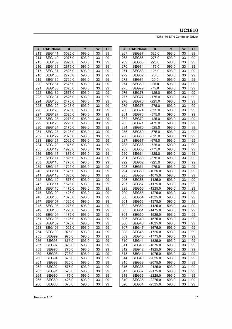
UC1610 128x160 STN Controller-Driver
Revision 1.11 57
# PAD Name X Y W H213 SEG141 3025.0 593.0 33 99214 SEG140 2975.0 593.0 33 99215 SEG139 2925.0 593.0 33 99216 SEG138 2875.0 593.0 33 99217 SEG137 2825.0 593.0 33 99218 SEG136 2775.0 593.0 33 99219 SEG135 2725.0 593.0 33 99220 SEG134 2675.0 593.0 33 99221 SEG133 2625.0 593.0 33 99222 SEG132 2575.0 593.0 33 99223 SEG131 2525.0 593.0 33 99224 SEG130 2475.0 593.0 33 99225 SEG129 2425.0 593.0 33 99226 SEG128 2375.0 593.0 33 99227 SEG127 2325.0 593.0 33 99228 SEG126 2275.0 593.0 33 99229 SEG125 2225.0 593.0 33 99230 SEG124 2175.0 593.0 33 99231 SEG123 2125.0 593.0 33 99232 SEG122 2075.0 593.0 33 99233 SEG121 2025.0 593.0 33 99234 SEG120 1975.0 593.0 33 99235 SEG119 1925.0 593.0 33 99236 SEG118 1875.0 593.0 33 99237 SEG117 1825.0 593.0 33 99238 SEG116 1775.0 593.0 33 99239 SEG115 1725.0 593.0 33 99240 SEG114 1675.0 593.0 33 99241 SEG113 1625.0 593.0 33 99242 SEG112 1575.0 593.0 33 99243 SEG111 1525.0 593.0 33 99244 SEG110 1475.0 593.0 33 99245 SEG109 1425.0 593.0 33 99246 SEG108 1375.0 593.0 33 99247 SEG107 1325.0 593.0 33 99248 SEG106 1275.0 593.0 33 99249 SEG105 1225.0 593.0 33 99250 SEG104 1175.0 593.0 33 99251 SEG103 1125.0 593.0 33 99252 SEG102 1075.0 593.0 33 99253 SEG101 1025.0 593.0 33 99254 SEG100 975.0 593.0 33 99255 SEG99 925.0 593.0 33 99256 SEG98 875.0 593.0 33 99257 SEG97 825.0 593.0 33 99258 SEG96 775.0 593.0 33 99259 SEG95 725.0 593.0 33 99260 SEG94 675.0 593.0 33 99261 SEG93 625.0 593.0 33 99262 SEG92 575.0 593.0 33 99263 SEG91 525.0 593.0 33 99264 SEG90 475.0 593.0 33 99265 SEG89 425.0 593.0 33 99266 SEG88 375.0 593.0 33 99
# PAD Name X Y W H267 SEG87 325.0 593.0 33 99268 SEG86 275.0 593.0 33 99269 SEG85 225.0 593.0 33 99270 SEG84 175.0 593.0 33 99271 SEG83 125.0 593.0 33 99272 SEG82 75.0 593.0 33 99273 SEG81 25.0 593.0 33 99274 SEG80 -25.0 593.0 33 99275 SEG79 -75.0 593.0 33 99276 SEG78 -125.0 593.0 33 99277 SEG77 -175.0 593.0 33 99278 SEG76 -225.0 593.0 33 99279 SEG75 -275.0 593.0 33 99280 SEG74 -325.0 593.0 33 99281 SEG73 -375.0 593.0 33 99282 SEG72 -425.0 593.0 33 99283 SEG71 -475.0 593.0 33 99284 SEG70 -525.0 593.0 33 99285 SEG69 -575.0 593.0 33 99286 SEG68 -625.0 593.0 33 99287 SEG67 -675.0 593.0 33 99288 SEG66 -725.0 593.0 33 99289 SEG65 -775.0 593.0 33 99290 SEG64 -825.0 593.0 33 99291 SEG63 -875.0 593.0 33 99292 SEG62 -925.0 593.0 33 99293 SEG61 -975.0 593.0 33 99294 SEG60 -1025.0 593.0 33 99295 SEG59 -1075.0 593.0 33 99296 SEG58 -1125.0 593.0 33 99297 SEG57 -1175.0 593.0 33 99298 SEG56 -1225.0 593.0 33 99299 SEG55 -1275.0 593.0 33 99300 SEG54 -1325.0 593.0 33 99301 SEG53 -1375.0 593.0 33 99302 SEG52 -1425.0 593.0 33 99303 SEG51 -1475.0 593.0 33 99304 SEG50 -1525.0 593.0 33 99305 SEG49 -1575.0 593.0 33 99306 SEG48 -1625.0 593.0 33 99307 SEG47 -1675.0 593.0 33 99308 SEG46 -1725.0 593.0 33 99309 SEG45 -1775.0 593.0 33 99310 SEG44 -1825.0 593.0 33 99311 SEG43 -1875.0 593.0 33 99312 SEG42 -1925.0 593.0 33 99313 SEG41 -1975.0 593.0 33 99314 SEG40 -2025.0 593.0 33 99315 SEG39 -2075.0 593.0 33 99316 SEG38 -2125.0 593.0 33 99317 SEG37 -2175.0 593.0 33 99318 SEG36 -2225.0 593.0 33 99319 SEG35 -2275.0 593.0 33 99320 SEG34 -2325.0 593.0 33 99
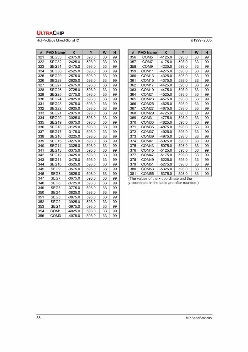
ULTRACHIP
High-Voltage Mixed-Signal IC ©1999~2005
58 MP Specifications
# PAD Name X Y W H321 SEG33 -2375.0 593.0 33 99322 SEG32 -2425.0 593.0 33 99323 SEG31 -2475.0 593.0 33 99324 SEG30 -2525.0 593.0 33 99325 SEG29 -2575.0 593.0 33 99326 SEG28 -2625.0 593.0 33 99327 SEG27 -2675.0 593.0 33 99328 SEG26 -2725.0 593.0 33 99329 SEG25 -2775.0 593.0 33 99330 SEG24 -2825.0 593.0 33 99331 SEG23 -2875.0 593.0 33 99332 SEG22 -2925.0 593.0 33 99333 SEG21 -2975.0 593.0 33 99334 SEG20 -3025.0 593.0 33 99335 SEG19 -3075.0 593.0 33 99336 SEG18 -3125.0 593.0 33 99337 SEG17 -3175.0 593.0 33 99338 SEG16 -3225.0 593.0 33 99339 SEG15 -3275.0 593.0 33 99340 SEG14 -3325.0 593.0 33 99341 SEG13 -3375.0 593.0 33 99342 SEG12 -3425.0 593.0 33 99343 SEG11 -3475.0 593.0 33 99344 SEG10 -3525.0 593.0 33 99345 SEG9 -3575.0 593.0 33 99346 SEG8 -3625.0 593.0 33 99347 SEG7 -3675.0 593.0 33 99348 SEG6 -3725.0 593.0 33 99349 SEG5 -3775.0 593.0 33 99350 SEG4 -3825.0 593.0 33 99351 SEG3 -3875.0 593.0 33 99352 SEG2 -3925.0 593.0 33 99353 SEG1 -3975.0 593.0 33 99354 COM1 -4025.0 593.0 33 99355 COM3 -4075.0 593.0 33 99
# PAD Name X Y W H356 COM5 -4125.0 593.0 33 99357 COM7 -4175.0 593.0 33 99358 COM9 -4225.0 593.0 33 99359 COM11 -4275.0 593.0 33 99360 COM13 -4325.0 593.0 33 99361 COM15 -4375.0 593.0 33 99362 COM17 -4425.0 593.0 33 99363 COM19 -4475.0 593.0 33 99364 COM21 -4525.0 593.0 33 99365 COM23 -4575.0 593.0 33 99366 COM25 -4625.0 593.0 33 99367 COM27 -4675.0 593.0 33 99368 COM29 -4725.0 593.0 33 99369 COM31 -4775.0 593.0 33 99370 COM33 -4825.0 593.0 33 99371 COM35 -4875.0 593.0 33 99372 COM37 -4925.0 593.0 33 99373 COM39 -4975.0 593.0 33 99374 COM41 -5025.0 593.0 33 99375 COM43 -5075.0 593.0 33 99376 COM45 -5125.0 593.0 33 99377 COM47 -5175.0 593.0 33 99378 COM49 -5225.0 593.0 33 99379 COM51 -5275.0 593.0 33 99380 COM53 -5325.0 593.0 33 99381 COM55 -5375.0 593.0 33 99
(The values of the x-coordinate and the y-coordinate in the table are after rounded.)

UC1610 128x160 STN Controller-Driver
Revision 1.11 59
TRAY INFORMATION
Tolerance
Roughness
Dim
ension
Angle
General
Date
09-17-03'
By
Draw
n
Jacky Wang
Specified
Unless O
therwise
Unit
Rev.
Checked
Approved
1 of 1Sheet
Size
Draw
ing No.
Material
Package C
ode
Scale
N/A
Proj.
AA4
Type: H
20-457×63-28(45)
2" IC T
ray
mm
ULT
RAC
HIP
INC.
晶 宏
半 導
體
N/A
N/A
drawing
see
detailA
lvinA
lvin
09-18-03'09-18-03'
SD
-212
ULTRACHIP
High-Voltage Mixed-Signal IC ©1999~2005
60 MP Specifications
REVISION HISTORY Version Contents Date of Rev.
0.6 Golden release Aug. 12, 2004
0.61 (1) The table is updated. (Section “ESD Consideration”, page 41) Aug. 16, 2004
(1) COG section presents. (Section “Recommended COG Layout”, page 7) (2) Gray-shade control percentages are updated.
LC[6:5] : 20%, 24%, 28%, 32% 24%, 29%, 36%, 40% (Section “Control Register”, page 9; ”Command Description”, page 15)
(3) The condition on VDD2 is adjusted: 2.5V 2.7V (Section “LCD Voltage Setting” – Load Driving Strength, page 21)
0.7
(4) Pad coordination information is updated. (Section “Pad Coordinates”, Pp 55 ~ 58)
Nov. 5, 2004
(1) In the “Operating Mode” table, the status of “Draining Circuit” in Sleep mode is corrected: “OFF” “ON”
(2) Most contents of subsection “Changing Operation Mode” are re-written. (Section “Reset & Power Management”, page 38)
(3) Subsection “Extended Display OFF” is removed. (4) Subsection “Brief Display OFF” is renamed as “Display OFF”.
(Section “Reset & Power Management”, page 40)
0.71
(5) COF drawings are removed. (Section “COF Information”, Pp 59 ~ 60)
Nov. 9, 2004
(1) The VLCD Formula is updated. (Section “VLCD Quick Reference”, page 22)
(2) A typo error is corrected: “8-shade” “4-shade” (Section “LCD Display Controls” - Clock & Timing Generator, page 24)
(3) In the I2C figure (Read Mode), the direction of some acknowledge signals (A) is modified from upward to downward. (Section “Host Interface” – 2-wire Serial Interface (I2C), page 30)
(4) SEG output impedance, RON (SEG), COM output impedance, RON (COM), and Average Line rate, fLINE, are adjusted. (Section “Specification” – DC Characteristics, page 44)
(5) Experiment data are corrected. (Section “Specification” – Power Consumption, page 44)
0.8
(6) For 8080, 6800, S8/S8uc, and S9 modes, Chip Select Setup Time tCSSD80, tCSSD68, tCSSDS8, tCSSDS9 are removed.
(7) Some AC timing data are adjusted. (Section “AC Characteristics”, Pp 45 ~ 51)
Nov. 30, 2004
(1) “COF” related contents are removed. (Overall)
(2) VDD for COG application is adjusted: 17V 17.5V (Section “Recommended COG Layout”, page 7)
(3) The default of APC0~1 is erased. (Section “Control Register”, page 9)
(4) The content of 2nd byte is corrected. (Section “Command Description” – (31) and (33), page 18)
1.0
(5) The contents of WR0 and WR1 for serial mode are modified. (Section “Host Interface”, page 27)
Feb. 16, 2005

UC1610 128x160 STN Controller-Driver
Revision 1.11 61
Version Contents Date of Rev.(6) The RAM table is corrected.
(Section “Display Data RAM”, page 38) (7) Point 2 is updated.
(Section “ESD Consideration”, page 42) (8) Some AC timings are updated.
(Section “AC Characteristics”, page 49)
1.0
(9) The presentation of Bump Height is modified. (Section “Physical Dimension”, page 53)
Feb. 16, 2005
1.01 (1) Figures 14 and 15, for Power Up/Down Sequence, are fixed. (Section “Reset and Power Management”, page 40) Feb. 18, 2005
(1) Some description for absolute maximum ratings is revised (Section “Absolute Maximum Ratings”, page 43) (2) Serial Mode VIL and VIH are adjusted: 0.2VDD/ 0.8VDD 0.15VDD/0.85VDD (Section “Specifications”, page 44) 1.1
(3) Delete Max Output Disable Time (Section “AC Characteristics”, Pp 45 and 47 )
Mar. 25, 2005
1.11 (1) Remove without I2C interface version Apr. 13, 2005