Ultrabright Room-Temperature Sub-Nanosecond Emission from...
8
Ultrabright Room-Temperature Sub-Nanosecond Emission from Single Nitrogen-Vacancy Centers Coupled to Nanopatch Antennas Simeon I. Bogdanov,* ,†,‡ Mikhail Y. Shalaginov, †,‡ Alexei S. Lagutchev, †,‡ Chin-Cheng Chiang, †,‡ Deesha Shah, †,‡ Alexandr S. Baburin, §,∥ Ilya A. Ryzhikov, §,⊥ Ilya A. Rodionov, §,∥ Alexander V. Kildishev, †,‡ Alexandra Boltasseva, †,‡ and Vladimir M. Shalaev †,‡ † School of Electrical & Computer Engineering and Birck Nanotechnology Center, Purdue University, West Lafayette, Indiana 47907, United States ‡ Purdue Quantum Center, Purdue University, West Lafayette, Indiana 47907, United States § FMNS REC, Bauman Moscow State Technical University, Moscow 105005, Russia ∥ Dukhov Research Institute of Automatics, Moscow 127055, Russia ⊥ Institute for Theoretical and Applied Electromagnetics RAS, Moscow 125412, Russia * S Supporting Information ABSTRACT: Solid-state quantum emitters are in high demand for emerging technologies such as advanced sensing and quantum information processing. Generally, these emitters are not sufficiently bright for practical applications, and a promising solution consists in coupling them to plasmonic nanostructures. Plasmonic nanostructures support broadband modes, making it possible to speed up the fluorescence emission in room-temperature emitters by several orders of magnitude. However, one has not yet achieved such a fluorescence lifetime shortening without a substantial loss in emission efficiency, largely because of strong absorption in metals and emitter bleaching. Here, we demonstrate ultrabright single-photon emission from photostable nitrogen-vacancy (NV) centers in nanodiamonds coupled to plasmonic nanocavities made of low-loss single-crystalline silver. We observe a 70-fold difference between the average fluorescence lifetimes and a 90-fold increase in the average detected saturated intensity. The nanocavity-coupled NVs produce up to 35 million photon counts per second, several times more than the previously reported rates from room- temperature quantum emitters. KEYWORDS: Quantum plasmonics, nitrogen-vacancy centers, single-photon source, nanodiamonds, nanopatch antennas, epitaxial silver S ingle-photon emitters, 1 such as single molecules, quantum dots, color centers in crystals, or rare-earth atoms, are of great interest for applications in quantum information processing, 2 quantum chemistry, 3 and biology. 4 These quantum sources emit light with unique properties including antibunching, absence of ensemble broadening, extreme sensitivity to the local environment, and, in some cases, photon indistinguishability. 5−8 These emitters are usually very dim, making it challenging to harness their emission. Typical detected photon rates from bare quantum emitters are in the range from 10 4 to 10 5 counts per second (cps), 1 only rarely exceeding 10 6 cps. 9−11 The most fundamental limiting factors for the detected photon rate from quantum emitters are radiative lifetime and photon collection efficiency. By solely increasing the collection efficiency, 12−17 detected photon rates from single emitters can exceed 10 6 cps. 16,17 Another approach for brightness enhancement hinges on drastically increasing the local density of states (LDOS) in the vicinity of the emitter, leading to a faster photon emission. 18 Dielectric 19−21 and plasmonic 22 resonators are typically used for LDOS enhance- ment, with alternative approaches relying on slow light 23,24 and metamaterial dispersion. 25,26 The local density of states is proportional to the ratio of the resonance quality factor to the volume where the field is localized. In accord with this, LDOS enhancement is typically achieved by using either highly resonant but relatively large (diffraction-limited) dielectric structures or plasmonic nano- structures with lower resonance quality factors but smaller, subdiffraction size volumes. Dielectric resonators and slow light waveguides enhance the LDOS by increasing the interaction time between the dipole and the emitted field. However, as the quality factor Q of the dielectric structure increases, the long photon storage time becomes an impedi- Received: April 9, 2018 Revised: June 22, 2018 Published: July 3, 2018 Letter pubs.acs.org/NanoLett Cite This: Nano Lett. XXXX, XXX, XXX-XXX © XXXX American Chemical Society A DOI: 10.1021/acs.nanolett.8b01415 Nano Lett. XXXX, XXX, XXX−XXX Downloaded via MASSACHUSETTS INST OF TECHNOLOGY on July 22, 2018 at 16:09:36 (UTC). See https://pubs.acs.org/sharingguidelines for options on how to legitimately share published articles.
Transcript of Ultrabright Room-Temperature Sub-Nanosecond Emission from...
Ultrabright Room-Temperature Sub-Nanosecond Emission fromSingle Nitrogen-Vacancy Centers Coupled to Nanopatch AntennasSimeon I. Bogdanov,*,†,‡ Mikhail Y. Shalaginov,†,‡ Alexei S. Lagutchev,†,‡ Chin-Cheng Chiang,†,‡
Deesha Shah,†,‡ Alexandr S. Baburin,§,∥ Ilya A. Ryzhikov,§,⊥ Ilya A. Rodionov,§,∥
Alexander V. Kildishev,†,‡ Alexandra Boltasseva,†,‡ and Vladimir M. Shalaev†,‡
†School of Electrical & Computer Engineering and Birck Nanotechnology Center, Purdue University, West Lafayette, Indiana47907, United States‡Purdue Quantum Center, Purdue University, West Lafayette, Indiana 47907, United States§FMNS REC, Bauman Moscow State Technical University, Moscow 105005, Russia∥Dukhov Research Institute of Automatics, Moscow 127055, Russia⊥Institute for Theoretical and Applied Electromagnetics RAS, Moscow 125412, Russia
*S Supporting Information
ABSTRACT: Solid-state quantum emitters are in high demand for emergingtechnologies such as advanced sensing and quantum information processing.Generally, these emitters are not sufficiently bright for practical applications,and a promising solution consists in coupling them to plasmonicnanostructures. Plasmonic nanostructures support broadband modes, makingit possible to speed up the fluorescence emission in room-temperature emittersby several orders of magnitude. However, one has not yet achieved such afluorescence lifetime shortening without a substantial loss in emissionefficiency, largely because of strong absorption in metals and emitterbleaching. Here, we demonstrate ultrabright single-photon emission fromphotostable nitrogen-vacancy (NV) centers in nanodiamonds coupled toplasmonic nanocavities made of low-loss single-crystalline silver. We observe a70-fold difference between the average fluorescence lifetimes and a 90-foldincrease in the average detected saturated intensity. The nanocavity-coupledNVs produce up to 35 million photon counts per second, several times more than the previously reported rates from room-temperature quantum emitters.
KEYWORDS: Quantum plasmonics, nitrogen-vacancy centers, single-photon source, nanodiamonds, nanopatch antennas,epitaxial silver
Single-photon emitters,1 such as single molecules, quantumdots, color centers in crystals, or rare-earth atoms, are of
great interest for applications in quantum informationprocessing,2 quantum chemistry,3 and biology.4 Thesequantum sources emit light with unique properties includingantibunching, absence of ensemble broadening, extremesensitivity to the local environment, and, in some cases,photon indistinguishability.5−8 These emitters are usually verydim, making it challenging to harness their emission.Typical detected photon rates from bare quantum emitters
are in the range from 104 to 105 counts per second (cps),1 onlyrarely exceeding 106 cps.9−11 The most fundamental limitingfactors for the detected photon rate from quantum emitters areradiative lifetime and photon collection efficiency. By solelyincreasing the collection efficiency,12−17 detected photon ratesfrom single emitters can exceed 106 cps.16,17 Another approachfor brightness enhancement hinges on drastically increasing thelocal density of states (LDOS) in the vicinity of the emitter,leading to a faster photon emission.18 Dielectric19−21 and
plasmonic22 resonators are typically used for LDOS enhance-ment, with alternative approaches relying on slow light23,24 andmetamaterial dispersion.25,26
The local density of states is proportional to the ratio of theresonance quality factor to the volume where the field islocalized. In accord with this, LDOS enhancement is typicallyachieved by using either highly resonant but relatively large(diffraction-limited) dielectric structures or plasmonic nano-structures with lower resonance quality factors but smaller,subdiffraction size volumes. Dielectric resonators and slowlight waveguides enhance the LDOS by increasing theinteraction time between the dipole and the emitted field.However, as the quality factor Q of the dielectric structureincreases, the long photon storage time becomes an impedi-
Received: April 9, 2018Revised: June 22, 2018Published: July 3, 2018
Letter
pubs.acs.org/NanoLettCite This: Nano Lett. XXXX, XXX, XXX−XXX
© XXXX American Chemical Society A DOI: 10.1021/acs.nanolett.8b01415Nano Lett. XXXX, XXX, XXX−XXX
Dow
nloa
ded
via
MA
SSA
CH
USE
TT
S IN
ST O
F T
EC
HN
OL
OG
Y o
n Ju
ly 2
2, 2
018
at 1
6:09
:36
(UT
C).
Se
e ht
tps:
//pub
s.ac
s.or
g/sh
arin
ggui
delin
es f
or o
ptio
ns o
n ho
w to
legi
timat
ely
shar
e pu
blis
hed
artic
les.
ment to faster emission and limits the lifetime shortening.27
Alternatively, plasmonic nanostructures ensure broadband (i.e.,low-Q) LDOS enhancement, and their theoretical potential forlifetime shortening is about 2 orders of magnitude higher.28
The shortcoming of plasmonic nanostructures is the high lossresulting from nonradiative quenching of excitation andplasmon absorption in metals.Nanostructures with gap−surface−plasmon or metal−
insulator−metal (MIM) modes alleviate the quenchingproblem. Despite their proximity to the metal, the couplingrate of the emitter to the gap-plasmonic mode is comparable tothe quenching rate even as the gap shrinks below 10 nm.29,30
Furthermore, forming a gap-plasmon resonator by replacingthe top metal layer with a nanoparticle results in a nanopatchantenna (NPA) geometry.31 The NPAs radiate electro-magnetic energy on a time scale comparable to the plasmonlifetime,32 which mitigates plasmon absorption. Still, thanks tonanosized gaps, the concentration of the electromagnetic fieldin NPAs is sufficient to observe strong emitter−plasmoncoupling at room temperature.33 As a result, NPAs areemerging as the systems of choice for enhancing the brightnessof nanoscale emitters.34,35 Impressive results of single-photonemission in NPAs have been recently demonstrated usingcolloidal quantum dots with a strong lifetime shortening,antibunching photon statistics, and photon counts exceeding 1Mcps.36 Nevertheless, due to photobleaching of quantum dotsused in that experiment, it was not possible to reach thesaturation regime and assess the emitter efficiency. The fullpotential of quantum emitter brightness enhancement byplasmonic nanoantennas still remains to be realized.To overcome the problem of photostability and reduce
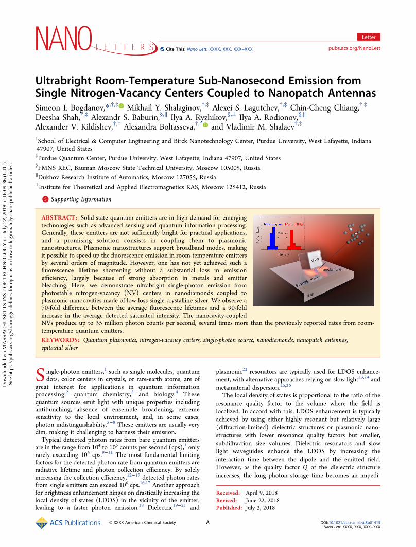
plasmonic losses, in this work, we use a nitrogen-vacancy (NV)center37 in a nanodiamond coupled to an all-crystalline-silverNPA (see Figure 1). The photostability of NV centerscombined with an ultralow loss of the silver film (ε″ = 0.11at 650 nm, see the Supporting Information, section I) leads todetected brightness in the range of tens of Mcps. By observing
fluorescence saturation and radiation patterns, we were able toquantify the factors leading to the brightness enhancement.
Results. Sample Design and Fabrication. In our experi-ment, the NVs were hosted by nanodiamonds with a diameterof dND = 20 ± 5 nm, where each nanodiamond nominallycontained 1−2 NVs. Two main samples were used in thestudy: one sample containing nanodiamonds with NVscoupled to NPAs and a bare glass coverslip substrate withdispersed nanodiamonds. The sample with NPAs wasfabricated according to the procedure well documented inprior works.31,36,38 We deposited a 35 nm thin low-loss,epitaxial silver and an approximately 6 nm thick dielectricspacer. The latter was formed using layer-by-layer alternatedeposition of poly(allyalamine hydrochloride) (PAH) andpolystyrenesulfonate (PSS). Nanodiamonds and subsequently100 nm size single-crystalline nanocubes were randomlydispersed on the spacer layer. This step resulted in therandom formation of NPAs with NV centers inside (see insetof Figure 1). To highlight the role of an epitaxial substrate, asimilar sample was made using polycrystalline silver. We foundthat the polycrystalline sample exhibits at least 5 times higherlosses than the epitaxial film at the wavelengths of interest (seediscussion below and Figure S5). The control sample wasfabricated by randomly dispersing the nanodiamonds on a glasscoverslip substrate with refractive index n = 1.525. In thecontrol experiment, we measured the photophysical character-istics of 14 single NV centers.
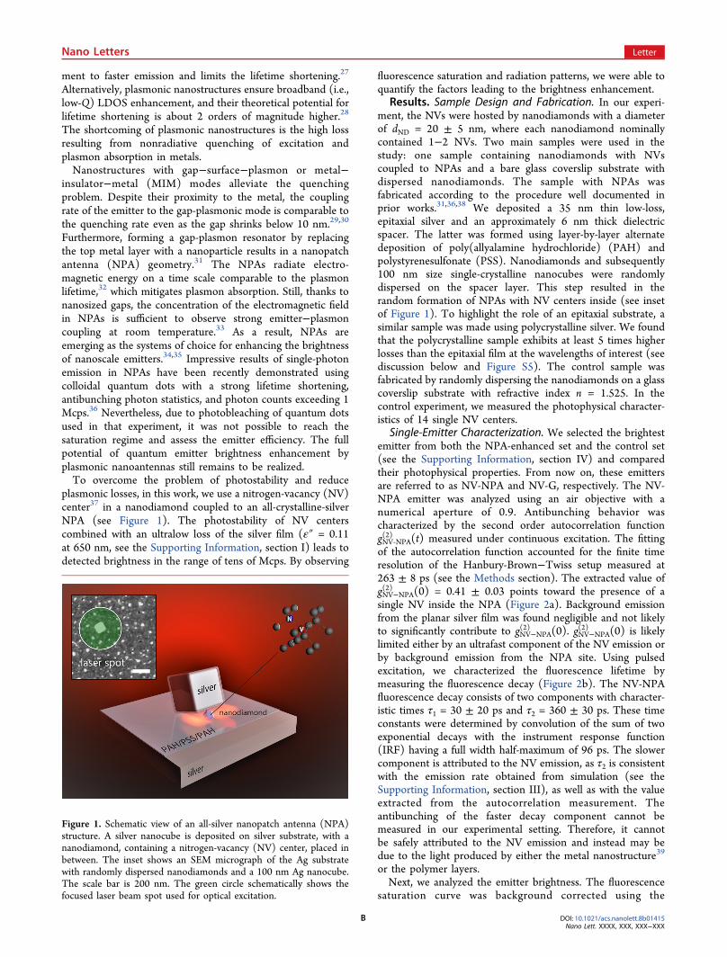
Single-Emitter Characterization. We selected the brightestemitter from both the NPA-enhanced set and the control set(see the Supporting Information, section IV) and comparedtheir photophysical properties. From now on, these emittersare referred to as NV-NPA and NV-G, respectively. The NV-NPA emitter was analyzed using an air objective with anumerical aperture of 0.9. Antibunching behavior wascharacterized by the second order autocorrelation functiongNV‑NPA(2) (t) measured under continuous excitation. The fittingof the autocorrelation function accounted for the finite timeresolution of the Hanbury-Brown−Twiss setup measured at263 ± 8 ps (see the Methods section). The extracted value ofgNV−NPA(2) (0) = 0.41 ± 0.03 points toward the presence of asingle NV inside the NPA (Figure 2a). Background emissionfrom the planar silver film was found negligible and not likelyto significantly contribute to gNV−NPA
(2) (0). gNV−NPA(2) (0) is likely
limited either by an ultrafast component of the NV emission orby background emission from the NPA site. Using pulsedexcitation, we characterized the fluorescence lifetime bymeasuring the fluorescence decay (Figure 2b). The NV-NPAfluorescence decay consists of two components with character-istic times τ1 = 30 ± 20 ps and τ2 = 360 ± 30 ps. These timeconstants were determined by convolution of the sum of twoexponential decays with the instrument response function(IRF) having a full width half-maximum of 96 ps. The slowercomponent is attributed to the NV emission, as τ2 is consistentwith the emission rate obtained from simulation (see theSupporting Information, section III), as well as with the valueextracted from the autocorrelation measurement. Theantibunching of the faster decay component cannot bemeasured in our experimental setting. Therefore, it cannotbe safely attributed to the NV emission and instead may bedue to the light produced by either the metal nanostructure39
or the polymer layers.Next, we analyzed the emitter brightness. The fluorescence
saturation curve was background corrected using the
Figure 1. Schematic view of an all-silver nanopatch antenna (NPA)structure. A silver nanocube is deposited on silver substrate, with ananodiamond, containing a nitrogen-vacancy (NV) center, placed inbetween. The inset shows an SEM micrograph of the Ag substratewith randomly dispersed nanodiamonds and a 100 nm Ag nanocube.The scale bar is 200 nm. The green circle schematically shows thefocused laser beam spot used for optical excitation.
Nano Letters Letter
DOI: 10.1021/acs.nanolett.8b01415Nano Lett. XXXX, XXX, XXX−XXX
B
autocorrelation data. The fraction of the emission due to thebackground in the linear regime rbg has been calculated as
r g1 1 (0)bg(2)= − − .16 The linear background component
plotted in Figure 2c with the red dashed line has beensubtracted from the raw saturation data. This linearcomponent possibly originated from the same source as thefast component of the fluorescence decay. The remainingsaturable component (red curve) yields INV‑NVA
sat = 56.3 ± 1.5Mcps. The saturating laser power (measured before couplingto the objective) was PNV‑NVA
sat = 1.20 ± 0.06 mW. In Figure 2d,we compare the spectra of nanoantenna scattering and NV-NPA emission. The dark field scattering spectrum from NV-NPA overlaps well with the photoluminescence spectrum ofthe coupled emitter. We conclude that the enhanced emissionindeed resulted from coupling of the NV to the mode of theNPA.The NV-G source was analyzed using an oil immersion
objective with numerical aperture (NA) = 1.49 in the totalinternal reflection mode. The photon purity was characterizedby an autocorrelation at zero delay of gNV‑G
(2) (0) = 0.21 ± 0.03,limited by the background fluorescence from the coverslipglass. The measured fluorescence lifetime was τNV‑G = 43.7 ±0.4 ns, which is over 120 times longer than in the case of theNV-NPA. We extract the saturated intensity of INV‑G
sat = 520 ± 7kcps, over 100 times weaker than for NV-NPA. The saturatinglaser power of PNV‑G
sat = 5.3 ± 0.09 mW is of the same order asthat of NV-NPA. The photoluminescence spectrum of NV-Gplotted on Figure 2d extends from 570 to 780 nm andindicates that both charge states NV0 and NV− likelycontribute to the emission.40
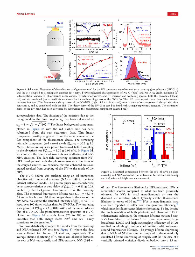
We now statistically compare the results from the coverslipand NPA-enhanced NV sets (see Figure 3), where the datawere collected for 14 and 11 emitters, respectively. Theaverage lifetime shortening of 70 times was observed betweenthe sets of NVs on coverslip and NPA-enhanced NVs (0.93 vs
62 ns). The fluorescence lifetime for NPA-enhanced NVs isremarkably shorter compared to what has been previouslyobserved for NVs in small nanodiamonds or near thediamond−air interface, which typically exhibit fluorescencelifetimes in excess of 10 ns.41,42 NVs in nanodiamonds havealso been reported to suffer from low quantum efficiency,43
which impedes fluorescence lifetime shortening. So far, despitethe implementation of both photonic and plasmonic LDOSenhancement techniques, the emission lifetimes obtained withNVs have failed to fall below 1 ns. In our experiment, largebroadband LDOS and high outcoupling efficiency of NPAsresulted in ultrabright antibunched emitters with sub-nano-second fluorescence lifetimes. The average lifetime shorteningdue to NPAs of 70 times can be compared to the numericallysimulated lifetime shortening of roughly 220 (in the case of avertically oriented emission dipole embedded into a 15 nm
Figure 2. Schematic illustration of the collection configurations used for the NV center in a nanodiamond on a coverslip glass substrate (NV-G, a)and the NV coupled to a nanopatch antenna (NV-NPA, b).Photophysical characterization of NV-G (blue) and NV-NPA (red), including (c)autocorrelation curves, (d) fluorescence decay curves, (e) saturation curves, and (f) emission and scattering spectra. Both the convoluted (solidred) and deconvoluted (dotted red) fits are shown for the antibunching curve of the NV-NPA. The IRF curve in part b describes the instrumentresponse function. The fluorescence decay curve of the NV-NPA (light pink) is fitted (red) using a sum of two exponential decays with timeconstants τ1 and τ2 convoluted with the IRF. The decay curve of the NV-G in part b is fitted with a single-exponential function. The saturationcurve of the NV-NPA has been corrected by subtracting the background component (dashed red).
Figure 3. Statistical comparison between the sets of NVs on glasscoverslip and NPA-enhanced NVs in terms of (a) lifetime shorteningand (b) saturated brightness enhancement.
Nano Letters Letter
DOI: 10.1021/acs.nanolett.8b01415Nano Lett. XXXX, XXX, XXX−XXX
C
diameter spherical nanodiamond). The discrepancy betweenthe two values can be attributed to an imperfect spectraloverlap between the cavity and NV radiation spectrum, amisalignment between the dipole orientation and local electricfield of the cavity mode and nonunity quantum yield of NVs innanodiamonds.The average saturated brightness is 90 times higher on
average in NPA-enhanced NVs than for the NVs on coverslip,which were analyzed using an oil objective with NA = 1.49 (20vs 0.22 Mcps, see Figure 3b). We note that the fluorescencelifetime characteristics of the NPA-enhanced emitters on thepolycrystalline-silver substrate are comparable to thoseobserved with epitaxial silver. However, due to higher lossesof the polycrystalline silver, the saturated emission was onaverage several times weaker than that on epitaxial silversubstrate (2.8 vs 20.0 Mcps). The characterization data forseveral additional NPA-enhanced emitters on epitaxial andpolycrystalline-silver substrates are shown in Figures S4 andS5, respectively. Furthermore, we characterized saturatedintensity for 8 NVs on coverslip using an air objective withNA = 0.9, with access from the air side, and found 0.066 Mcpson average. For those NVs, autocorrelation was not verified, sothis number represents an upper bound on the averagesaturated intensity for single NVs. Compared to NVs oncoverslip analyzed with the air objective, the NPA-enhancedset presents an average increase in brightness of 300 times.Table 1 summarizes the average photophysical properties ofthe NV sets.Despite a drastic lifetime shortening compared to the set of
NVs on coverslip, the emission of NPA-enhanced NVs issaturated at a comparable excitation laser power. One canconclude that the excitation rate at constant pump power isalso strongly enhanced by the NPA. By comparing the averagespecific excitation rates cexc = γtot/Psat between the coverslipand NPA-enhanced NV sets, and accounting for the differencebetween numerical apertures used for pump delivery in bothexperiments, we find an increase in NV absorption cross-section of 200 times due to the NPA. The enhancement ofboth emission and absorption is a consequence of multiplebroad resonances present in NPAs.44 It was previously shownthat, at high incident pump powers, the properties of theoptical modes in NPAs were altered due to structuraldeformation.39 Strong local enhancement of pump intensityin NPAs allows to obtain the same excitation rate at a reducedtotal incident pump power. Therefore, the local pumpenhancement is important to guarantee a high emitterbrightness without degrading the antenna properties. In thefuture, these resonances could be engineered45 to preciselymatch the absorption and emission frequencies of narrow-bandemitters, yielding an even larger intensity enhancement andbetter photon purity.46
Extraction of Emitter Efficiency. The increase in saturatedbrightness provided by the NPAs is commensurate with theobserved lifetime shortening, suggesting that these plasmonicnanostructures are highly efficient. However, to account for the
influence of different factors leading to the detected brightnessenhancement, we perform a quantitative efficiency analysis.The total emitter efficiency ηtot = Isat/γtot is defined as the ratiobetween the detected saturated fluorescence intensity Isat andthe total decay rate γtot. The average total emitter efficiencywas found to be almost identical between the NPA-enhancedset and the coverslip set (about 1.2% in both cases). Thesevalues depend on the efficiency parameters of the microscopesetup. To obtain an instrument-independent quantity, wecalculate the photon efficiency ηph, i.e., the number of photonsemitted into the far-field per NV excitation event. The photonefficiency can be either calculated from the assumed micro-scopic properties of the photon source or deduced from theobserved total fluorescence intensity. We use both approachesto estimate, respectively, the upper (ηph,sim) and lower (ηph,meas)bounds for the photon efficiency of NPA-enhanced NVs andNVs on coverslip. These quantities are summarized in Table 2.
The upper bound for photon efficiency is obtained from full-field simulations. We define the simulated photon efficiency as
ph,simff
ff loss nrη γγ γ γ
=+ + (1)
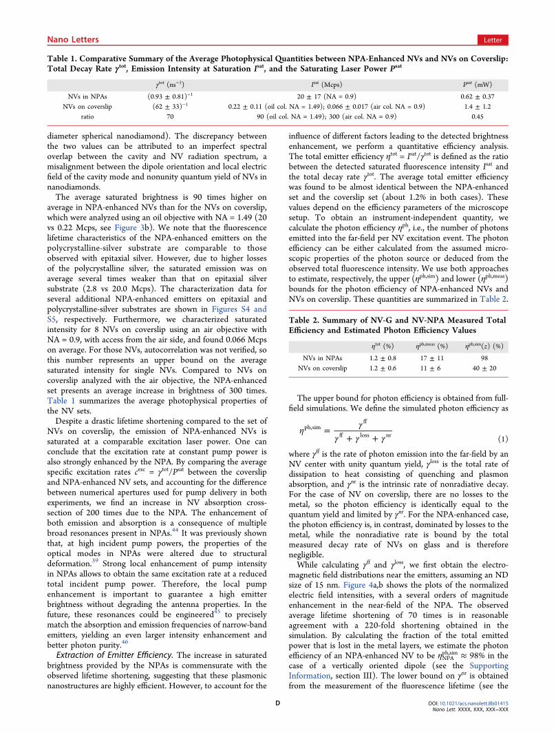
where γff is the rate of photon emission into the far-field by anNV center with unity quantum yield, γloss is the total rate ofdissipation to heat consisting of quenching and plasmonabsorption, and γnr is the intrinsic rate of nonradiative decay.For the case of NV on coverslip, there are no losses to themetal, so the photon efficiency is identically equal to thequantum yield and limited by γnr. For the NPA-enhanced case,the photon efficiency is, in contrast, dominated by losses to themetal, while the nonradiative rate is bound by the totalmeasured decay rate of NVs on glass and is thereforenegligible.While calculating γff and γloss, we first obtain the electro-
magnetic field distributions near the emitters, assuming an NDsize of 15 nm. Figure 4a,b shows the plots of the normalizedelectric field intensities, with a several orders of magnitudeenhancement in the near-field of the NPA. The observedaverage lifetime shortening of 70 times is in reasonableagreement with a 220-fold shortening obtained in thesimulation. By calculating the fraction of the total emittedpower that is lost in the metal layers, we estimate the photonefficiency of an NPA-enhanced NV to be ηNPA
ph,sim ≈ 98% in thecase of a vertically oriented dipole (see the SupportingInformation, section III). The lower bound on γnr is obtainedfrom the measurement of the fluorescence lifetime (see the
Table 1. Comparative Summary of the Average Photophysical Quantities between NPA-Enhanced NVs and NVs on Coverslip:Total Decay Rate γtot, Emission Intensity at Saturation Isat, and the Saturating Laser Power Psat
γtot (ns−1) Isat (Mcps) Psat (mW)
NVs in NPAs (0.93 ± 0.81)−1 20 ± 17 (NA = 0.9) 0.62 ± 0.37NVs on coverslip (62 ± 33)−1 0.22 ± 0.11 (oil col. NA = 1.49); 0.066 ± 0.017 (air col. NA = 0.9) 1.4 ± 1.2
ratio 70 90 (oil col. NA = 1.49); 300 (air col. NA = 0.9) 0.45
Table 2. Summary of NV-G and NV-NPA Measured TotalEfficiency and Estimated Photon Efficiency Values
ηtot (%) ηph,meas (%) ηph,sim(z) (%)
NVs in NPAs 1.2 ± 0.8 17 ± 11 98NVs on coverslip 1.2 ± 0.6 11 ± 6 40 ± 20
Nano Letters Letter
DOI: 10.1021/acs.nanolett.8b01415Nano Lett. XXXX, XXX, XXX−XXX
D
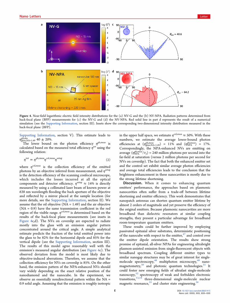
Supporting Information, section V). This estimate leads toηglass,NA=1.49ph,sim 40 ± 20%.The lower bound on the photon efficiency ηph,meas is
calculated based on the measured total efficiency ηtot using thefollowing relation:
tot ph,meas col,meas setupη η η η= (2)
where ηcol,meas is the collection efficiency of the emittedphotons by an objective inferred from measurement, and ηsetup
is the detection efficiency of the scanning confocal microscope,which includes the losses incurred at all the opticalcomponents and detector efficiency. ηsetup ≈ 14% is directlymeasured by using a collimated laser beam of known power at638 nm wavelength flooding the back aperture of the objectiveand reflected by a mirror placed at the sample location (formore details, see the Supporting Information, section II). Weassume that the oil objective (NA = 1.49) and the air objective(NA = 0.9) have the same transmission coefficient in the redregion of the visible range. ηcol,meas is determined based on theresults of the back-focal plane measurements (see insets inFigure 4c,d). The NVs on coverslip are expected to radiatemostly into the glass with an emission angular patternconcentrated around the critical angle. A simple analyticalestimate predicts the fraction of the total emitted power intothe glass to be 82% for the horizontal dipole and 85% for thevertical dipole (see the Supporting Information, section III).The results of this model agree reasonably well with theemission’s measured angular distribution (see Figure 4c). Theobserved deviation from the model is most likely due toobjective-induced aberrations. Therefore, we assume that thecollection efficiency for NVs on coverslip is 85%. On the otherhand, the emission pattern of the NPA-enhanced NVs shouldvary widely depending on the exact relative position of thenanodiamond and the nanocube. In the experiment, weobserve an essentially nondirectional pattern within the NA =0.9 solid angle. Assuming that the emission is roughly isotropic
in the upper half space, we estimate ηcol,meas ≈ 50%. With thesenumbers, we estimate the average lower-bound photonefficiencies at ⟨ηglass,NA=1.49
ph,meas ⟩ = 11% and ⟨ηNPAph,meas⟩ = 17%.
Correspondingly, the NPA-enhanced NVs are emitting onaverage ⟨ηNPA
ph,meas/τ2⟩ = 240 million photons per second into thefar-field at saturation (versus 2 million photons per second forNVs on coverslip). The fact that both the enhanced emitter setand the control set exhibit similar average photon efficienciesand average total efficiencies leads to the conclusion that thebrightness enhancement in these nanocavities is mostly due tothe strong lifetime shortening.
Discussion. When it comes to enhancing quantumemitters’ performance, the approaches based on plasmonicnanocavities often suffer from a trade-off between lifetimeshortening and emitter efficiency. This work demonstrates thatnanopatch antennas can shorten quantum emitter lifetime byalmost 2 orders of magnitude and yet preserve the efficiency ofthe original emitters. Because plasmonic nanocavities are morebroadband than dielectric resonators at similar couplingstrengths, they present a particular advantage for broadbandroom-temperature quantum emitters.These results could be further improved by employing
passivated epitaxial silver substrates, deterministic positioningof the nanocube with respect to the emitter,47 and control overthe emitter dipole orientation. The results show strongpromise of epitaxial, all-silver NPAs for engineering ultrabrightplasmon-assisted emission from single-fluorescent objects withbroadband spectrum. Coupling different emitter types tosimilar nanogap structures may be of great interest for single-molecule spectroscopy,48 multiphoton microscopy,49 nano-magnetometry,50 and photonic quantum technologies.51 Itcould foster new emerging fields of ultrafast single-moleculenanoscopy,52 spectroscopy of weak and forbidden electronictransitions,53,54 three-dimensional single-molecule nuclearmagnetic resonance,55 and cluster state engineering.56
Figure 4. Near-field logarithmic electric field intensity distributions for the (a) NV-G and the (b) NV-NPA. Radiation patterns determined fromback-focal plane (BFP) measurements for (c) the NV-G and (d) the NV-NPA. Red solid line in part d represents the result of a numericalsimulation (see the Supporting Information, section III). Insets show the corresponding two-dimensional intensity distribution measured in theback-focal plane (BFP).
Nano Letters Letter
DOI: 10.1021/acs.nanolett.8b01415Nano Lett. XXXX, XXX, XXX−XXX
E

Specifically, in the case of NV centers, strong enhancementof brightness by plasmonic nanoantennas could result in asensitive single-shot readout of the electron spin at roomtemperature. The spin coherence time of NV centers in ournanodiamonds without coupling to the NPAs is on the orderof 1 μs, probably limited by impurities inside and at the surfaceof the nanodiamonds. For magnetometry and quantuminformation applications, this coherence time can be improvedthrough surface treatment, employing seeded nanodiamondgrowth and applying refocusing techniques.Methods. Sample Fabrication. The coverslip sample was
prepared by coating the coverslip surface with one PAHmonolayer and dropcasting a diluted water solution of 20 nmnanodiamonds for 10 s (Adamas Nano) before rinsing thesurface with water. Polycrystalline 50 nm silver films weredeposited on Si substrate with a 10 nm Ti adhesion layer.Epitaxial silver films were 35 nm thick and deposited directlyon Si substrate at the BMSTU Nanofabrication Facility(Functional Micro/Nanosystems, FMNS REC, ID 74300).Three self-assembled monolayers (PAH/PSS/PAH) weredeposited by alternately dipping the samples with the silverfilms into the corresponding solutions for 5 min. A dilutedwater solution of 20 nm nanodiamonds was then dropcast ontothe PAH surface. Finally, a 20× diluted water/ethanol solutionof 100 nm crystalline nanocubes (Nanocomposix) wasdropcast on the sample.Characterization. All the optical characterization was
performed using a custom-made scanning confocal microscopewith a 50 μm pinhole based on a commercial invertedmicroscope body (Nikon Ti−U). The optical pumping in allthe experiments except the lifetime measurement wasadministered by a DPSS 532 nm laser. Lifetime character-ization was performed using a 514 nm fiber-coupled diodelaser with a nominal 100 ps pulse width and adjustablerepetition rate in the 2−80 MHz range (BDL-514-SMNi,Becker & Hickl). The excitation beam was reflected off a 550nm long-pass dichroic mirror (DMLP550L, Thorlabs), and a550 nm long-pass filter (FEL0550, Thorlabs) was used to filterout the remaining pump power. Two avalanche detectors witha 30 ps time resolution and 35% quantum efficiency at 650 nm(PDM, Micro-Photon Devices) were used for single-photondetection during scanning, lifetime, and autocorrelationmeasurements. An avalanche detector with 69% quantumefficiency at 650 nm (SPCM-AQRH, Excelitas) was used forsaturation measurements. Time-correlated photon countingwas performed by an acquisition card with a 4 ps internal jitter(SPC-150, Becker & Hickl). The values of g(2)(0) wereextracted by accounting for the finite time resolution of theautocorrelation experiment δtinstr = 263 ± 8 ps. The measuredautocorrelation was fitted by a standard two-exponential modelg(2)τ = 1 − A exp(|τ|/τA) + B exp(|τ|/τB), convoluted with aGaussian of width δtinstr. The fitted autocorrelation at zerodelay was then taken equal to g(2)(0) = 1 − A + B.Simulation. All full-wave 3D electromagnetic numerical
simulations were performed using finite-element frequency-domain method with a commercial software (ComsolMultiphysics, Wave Optics Module). The simulation domainwas a cube with a side of 1.8 μm for NV-NPA and 2.4 μm forNV-G surrounded by a 400 nm thick perfectly matching layer.The optical emitter was modeled as an AC current densityinside a 2 nm diameter sphere enclosed by a 15 nm diameterdiamond shell. The emitter’s wavelength was fixed at 640 nm.The emitter had a vertical dipole orientation and was placed
between a 35 nm Ag layer and a Ag nanocube. The nanocubewas modeled having 8 nm curvature radius at its corners andcovered in 3 nm PVP layer with n = 1.4. One ridge of thenanocube’s bottom facet was in full contact with the spacer,while the nanodiamond supported the middle of the oppositeridge of the bottom facet. The spacer layer was modeled as anisotropic dielectric with n = 1.5.Simulated values in Table 2 are computed assuming a
vertical dipole orientation for both emitters. Vertical dipoleorientation for the NV-NPA is assumed dominant because ofthe relatively weak Purcell effect expected for both horizontalorientations (see Supporting Information, Section III).
■ ASSOCIATED CONTENT*S Supporting InformationThe Supporting Information is available free of charge on theACS Publications website at DOI: 10.1021/acs.nano-lett.8b01415.
Details about silver substrates’ dielectric permittivities,spacer preparation procedure, measurement of setupefficiency, simulation of the emitters’ total decay rates,loss rates and collection efficiencies, statistics ofreference emitter characteristics, calculation of thequantum yield of NVs in nanodiamonds, as well asantibunching curves, fluorescence decay curves, andsaturation curves for additional NPA-coupled emitterson epitaxial and polycrystalline-silver substrates (PDF)
■ AUTHOR INFORMATIONCorresponding Author*E-mail: [email protected] I. Bogdanov: 0000-0001-5608-546XAlexandra Boltasseva: 0000-0002-5988-7625Author ContributionsS. I. Bogdanov conceived the experiment and wrote the initialdraft of the paper. S. I. Bogdanov and C.-C. Chiang carried outthe quantum emitter characterization. M. Y. Shalaginov and A.V. Kildishev carried out the numerical simulations. S. I.Bogdanov and A. S. Lagutchev built the experimental setup. D.Shah carried out the ellipsometry characterization ofpolycrystalline-silver substrates and spacer layers as well asmeasurements of ensemble nanocavity scattering spectra. A. S.Baburin, I. A. Ryzhikov, and I. A. Rodionov grew the epitaxialsilver film. S. I. Bogdanov, A. S. Lagutchev, A. Boltasseva, andV. M. Shalaev interpreted the results. A. S. Lagutchev, M. Y.Shalaginov, D. Shah, A. Boltasseva, and V. M. Shalaevcontributed to writing the paper. A. Boltasseva and V. M.Shalaev supervised the project. All authors have given approvalto the final version of the manuscript.NotesThe authors declare no competing financial interest.
■ ACKNOWLEDGMENTSThe authors acknowledge O. Makarova for the AFMmeasurement of polycrystalline silver RMS roughness, and I.Aharonovich, M. Mikkelsen, A. Akimov, V. Vorobyov, and S.Bolshedvorskii for useful discussions. This work was partiallysupported by the U.S. Department of Energy, Office of BasicEnergy Sciences, Division of Materials Sciences and Engineer-ing under Award DE-SC0017717 (S. I. Bogdanov), the
Nano Letters Letter
DOI: 10.1021/acs.nanolett.8b01415Nano Lett. XXXX, XXX, XXX−XXX
F

National Science Foundation NSF-OP Grant DMR-1506775(D. Shah), and the Office of Naval Research (ONR) DURIPGrant N00014-16-1-2767 (equipment grant used to purchasethe scanning confocal microscope, lasers, detectors, and single-photon counting capability used in this work). A. V. Kildishevacknowledges the DARPA/DSO Extreme Optics and Imaging(EXTREME) Program, Award HR00111720032 (numericalmodeling and simulations).
■ REFERENCES(1) Aharonovich, I.; Englund, D.; Toth, M. Nat. Photonics 2016, 10,631−641.(2) O’Brien, J. L. Science 2007, 318, 1567−1570.(3) Moerner, W. E.; Shechtman, Y.; Wang, Q. Faraday Discuss. 2015,184, 9−36.(4) Sydor, A. M.; Czymmek, K. J.; Puchner, E. M.; Mennella, V.Trends Cell Biol. 2015, 25, 730−748.(5) Sipahigil, A.; Jahnke, K. D.; Rogers, L. J.; Teraji, T.; Isoya, J.;Zibrov, A. S.; Jelezko, F.; Lukin, M. D. Phys. Rev. Lett. 2014, 113,113602.(6) Somaschi, N.; Giesz, V.; De Santis, L.; Loredo, J. C.; Almeida, M.P.; Hornecker, G.; Portalupi, S. L.; Grange, T.; Anton, C.; Demory, J.;et al. Nat. Photonics 2016, 10, 340−345.(7) He, Y.-M.; He, Y.; Wei, Y.-J.; Wu, D.; Atature, M.; Schneider, C.;Hofling, S.; Kamp, M.; Lu, C.-Y.; Pan, J.-W. Nat. Nanotechnol. 2013,8, 213−217.(8) Muller, K.; Fischer, K. A.; Dory, C.; Sarmiento, T.; Lagoudakis,K. G.; Rundquist, A.; Kelaita, Y. A.; Vuckovic, J. Optica 2016, 3, 931.(9) Tran, T. T.; Bray, K.; Ford, M. J.; Toth, M.; Aharonovich, I. Nat.Nanotechnol. 2015, 11, 37−41.(10) Grosso, G.; Moon, H.; Lienhard, B.; Ali, S.; Efetov, D. K.;Furchi, M. M.; Jarillo-Herrero, P.; Ford, M. J.; Aharonovich, I.;Englund, D. Nat. Commun. 2017, 8, 705.(11) Neu, E.; Agio, M.; Becher, C. Opt. Express 2012, 20, 19956.(12) Mouradian, S. L.; Schroder, T.; Poitras, C. B.; Li, L.; Goldstein,J.; Chen, E. H.; Walsh, M.; Cardenas, J.; Markham, M. L.; Twitchen,D. J. Phys. Rev. X 2015, 5, 31009.(13) Babinec, T. M.; Hausmann, B. J. M.; Khan, M.; Zhang, Y.;Maze, J. R.; Hemmer, P. R.; Loncar, M. Nat. Nanotechnol. 2010, 5,195−199.(14) Hadden, J. P.; Harrison, J. P.; Stanley-Clarke, A. C.; Marseglia,L.; Ho, Y. L. D.; Patton, B. R.; O’Brien, J. L.; Rarity, J. G. Appl. Phys.Lett. 2010, 97, 402−406.(15) Riedel, D.; Rohner, D.; Ganzhorn, M.; Kaldewey, T.; Appel, P.;Neu, E.; Warburton, R. J.; Maletinsky, P. Phys. Rev. Appl. 2014, 2, 1−6.(16) Wan, N. H.; Shields, B. J.; Kim, D.; Mouradian, S.; Lienhard,B.; Walsh, M.; Bakhru, H.; Schroder, T.; Englund, D. Nano Lett. 2018,18, 2787−2793.(17) Momenzadeh, S. A.; Stohr, R. J.; de Oliveira, F. F.; Brunner, A.;Denisenko, A.; Yang, S.; Reinhard, F.; Wrachtrup, J. Nano Lett. 2015,15, 165−169.(18) Pelton, M. Nat. Photonics 2015, 9, 427−435.(19) Wolters, J.; Schell, A. W.; Kewes, G.; Nusse, N.; Schoengen, M.;Doscher, H.; Hannappel, T.; Lochel, B.; Barth, M.; Benson, O. Appl.Phys. Lett. 2010, 97, 2013−2016.(20) Riedrich-Moller, J.; Pezzagna, S.; Meijer, J.; Pauly, C.;Mucklich, F.; Markham, M.; Edmonds, A. M.; Becher, C. Appl.Phys. Lett. 2015, 106, 221103.(21) Benedikter, J.; Kaupp, H.; Hummer, T.; Liang, Y.; Bommer, A.;Becher, C.; Krueger, A.; Smith, J. M.; Hansch, T. W.; Hunger, D. Phys.Rev. Appl. 2017, 7, 024031.(22) Koenderink, A. F. ACS Photonics 2017, 4, 710−722.(23) Arcari, M.; Sollner, I.; Javadi, A.; Lindskov Hansen, S.;Mahmoodian, S.; Liu, J.; Thyrrestrup, H.; Lee, E. H.; Song, J. D.;Stobbe, S.; et al. Phys. Rev. Lett. 2014, 113, 1−5.(24) Goban, A.; Hung, C.-L.; Hood, J. D.; Yu, S.-P.; Muniz, J. A.;Painter, O.; Kimble, H. J. Phys. Rev. Lett. 2015, 115, 063601.
(25) Shalaginov, M. Y.; Vorobyov, V. V.; Liu, J.; Ferrera, M.;Akimov, A. V.; Lagutchev, A.; Smolyaninov, A. N.; Klimov, V. V.;Irudayaraj, J.; Kildishev, A. V.; et al. Laser Photon. Rev. 2015, 9, 120−127.(26) Lu, D.; Kan, J. J.; Fullerton, E. E.; Liu, Z. Nat. Nanotechnol.2014, 9, 48−53.(27) Sipahigil, A.; Evans, R. E.; Sukachev, D. D.; Burek, M. J.;Borregaard, J.; Bhaskar, M. K.; Nguyen, C. T.; Pacheco, J. L.; Atikian,H. A.; Meuwly, C.; et al. Science 2016, 354, 847−850.(28) Bozhevolnyi, S. I.; Khurgin, J. Optica 2016, 3, 1418−1421.(29) Yang, J.; Faggiani, R. M.; Lalanne, P. Nanoscale Horiz.Nanoscale Horiz 2016, 1, 11−13.(30) Kongsuwan, N.; Demetriadou, A.; Chikkaraddy, R.; Benz, F.;Turek, V. A.; Keyser, U. F.; Baumberg, J. J.; Hess, O. ACS Photonics2018, 5, 186−191.(31) Moreau, A.; Ciracì, C.; Mock, J. J.; Hill, R. T.; Wang, Q.; Wiley,B. J.; Chilkoti, A.; Smith, D. R. Nature 2012, 492, 86−89.(32) Faggiani, R.; Yang, J.; Lalanne, P. ACS Photonics 2015, 2,1739−1744.(33) Chikkaraddy, R.; de Nijs, B.; Benz, F.; Barrow, S. J.; Scherman,O. A.; Rosta, E.; Demetriadou, A.; Fox, P.; Hess, O.; Baumberg, J. J.Nature 2016, 535, 127−130.(34) Akselrod, G. M.; Argyropoulos, C.; Hoang, T. B.; Ciracì, C.;Fang, C.; Huang, J.; Smith, D. R.; Mikkelsen, M. H. Nat. Photonics2014, 8, 835−840.(35) Hoang, T. B.; Akselrod, G. M.; Argyropoulos, C.; Huang, J.;Smith, D. R.; Mikkelsen, M. H. Nat. Commun. 2015, 6, 7788.(36) Hoang, T. B.; Akselrod, G. M.; Mikkelsen, M. H. Nano Lett.2016, 16, 270−275.(37) Doherty, M. W.; Manson, N. B.; Delaney, P.; Jelezko, F.;Wrachtrup, J.; Hollenberg, L. C. L. Phys. Rep. 2013, 528, 1−45.(38) Mock, J. J.; Hill, R. T.; Degiron, A.; Zauscher, S.; Chilkoti, A.;Smith, D. R. Nano Lett. 2008, 8, 2245−2252.(39) Mertens, J.; Kleemann, M.-E.; Chikkaraddy, R.; Narang, P.;Baumberg, J. J. Nano Lett. 2017, 17, 2568−2574.(40) Aslam, N.; Waldherr, G.; Neumann, P.; Jelezko, F.; Wrachtrup,J. New J. Phys. 2013, 15, 13064.(41) Choy, J. T.; Hausmann, B. J. M.; Babinec, T. M.; Bulu, I.; Khan,M.; Maletinsky, P.; Yacoby, A.; Loncar, M. Nat. Photonics 2011, 5,738−743.(42) Liebermeister, L.; Petersen, F.; Munchow, A. v.; Burchardt, D.;Hermelbracht, J.; Tashima, T.; Schell, A. W.; Benson, O.; Meinhardt,T.; Krueger, A.; et al. Appl. Phys. Lett. 2014, 104, 031101.(43) Mohtashami, A.; Femius Koenderink, A. New J. Phys. 2013, 15,43017.(44) Lassiter, J. B.; McGuire, F.; Mock, J. J.; Ciracì, C.; Hill, R. T.;Wiley, B. J.; Chilkoti, A.; Smith, D. R. Nano Lett. 2013, 13, 5866−5872.(45) Akselrod, G. M.; Ming, T.; Argyropoulos, C.; Hoang, T. B.; Lin,Y.; Ling, X.; Smith, D. R.; Kong, J.; Mikkelsen, M. H. Nano Lett. 2015,15, 3578−3584.(46) Andersen, S. K. H.; Kumar, S.; Bozhevolnyi, S. I. Nano Lett.2017, 17, 3889−3895.(47) Bahari, B.; Tellez-Limon, R.; Kante, B. J. Appl. Phys. 2016, 120,93106.(48) Kinkhabwala, A.; Yu, Z.; Fan, S.; Avlasevich, Y.; Mullen, K.;Moerner, W. E. Nat. Photonics 2009, 3, 654−657.(49) Nicolodi, D.; Argence, B.; Zhang, W.; Le Targat, R.; Santarelli,G.; Le Coq, Y. Nat. Photonics 2014, 8, 219−223.(50) Rondin, L.; Tetienne, J. P.; Hingant, T.; Roch, J. F.; Maletinsky,P.; Jacques, V. Rep. Prog. Phys. 2014, 77, 56503.(51) O’Brien, J. L.; Furusawa, A.; Vuckovic, J. Nat. Photonics 2009, 3,687−695.(52) Piatkowski, L.; Accanto, N.; van Hulst, N. F. ACS Photonics2016, 3, 1401−1414.(53) Benz, F.; Schmidt, M. K.; Dreismann, A.; Chikkaraddy, R.;Zhang, Y.; Demetriadou, A.; Carnegie, C.; Ohadi, H.; de Nijs, B.;Esteban, R.; et al. Science 2016, 354, 726−729.
Nano Letters Letter
DOI: 10.1021/acs.nanolett.8b01415Nano Lett. XXXX, XXX, XXX−XXX
G
(54) Rivera, N.; Kaminer, I.; Zhen, B.; Joannopoulos, J. D.; Soljacic,M. Science 2016, 353, 263−269.(55) Lovchinsky, I.; Sushkov, A. O.; Urbach, E.; de Leon, N. P.;Choi, S.; De Greve, K.; Evans, R.; Gertner, R.; Bersin, E.; Muller, C.;et al. Science 2016, 351, 836−841.(56) Schwartz, I.; Cogan, D.; Schmidgall, E. R.; Don, Y.; Gantz, L.;Kenneth, O.; Lindner, N. H.; Gershoni, D. Science 2016, 354, 434−437.
Nano Letters Letter
DOI: 10.1021/acs.nanolett.8b01415Nano Lett. XXXX, XXX, XXX−XXX
H