Ultra-Low Power Flash MCU with LCD & EEPROM · Rev. 1.00 an a 01 Rev. 1.00 7 an a 01 HT69F2562...
194
Ultra-Low Power Flash MCU with LCD & EEPROM HT69F2562 Revision: V1.00 Date: �an�a�� ��� �01� �an�a�� ��� �01�
Transcript of Ultra-Low Power Flash MCU with LCD & EEPROM · Rev. 1.00 an a 01 Rev. 1.00 7 an a 01 HT69F2562...

Ultra-Low Power Flash MCU with LCD & EEPROM
HT69F2562
Revision: V1.00 Date: ana 01ana 01

Rev. 1.00 ana 01 Rev. 1.00 3 ana 01
HT69F2562Ultra-Low Power Flash MCU with LCD & EEPROM
HT69F2562Ultra-Low Power Flash MCU with LCD & EEPROM
Table of Contents
Features ................................................................................................................ 6CPU Feates ..............................................................................................................................Peipheal Feates ......................................................................................................................
General Description ............................................................................................. 7Block Diagram ...................................................................................................... 7Pin Assignment .................................................................................................... 8Pin Description .................................................................................................... 9Absolute Maximum Ratings .............................................................................. 11D.C. Characteristics ........................................................................................... 11
Opeating Voltage Chaacteistics .............................................................................................. 11Standb Cent Chaacteistics ................................................................................................1Opeating Cent Chaacteistics ..............................................................................................1
A.C. Characteristics ........................................................................................... 13High Speed Intenal Oscillato – HIRC – Feqenc Accac ..................................................13Low Speed Intenal Oscillato Chaacteistics – LIRC ...............................................................13Low Speed Cstal Oscillato Chaacteistics – LXT ..................................................................14Opeating Feqenc Chaacteistic Cves ..............................................................................14Sstem Stat Up Time Chaacteistics .......................................................................................14
Input/Output D.C. Characteristics .................................................................... 15Inpt/Otpt (withot Mlti-powe) D.C. Chaacteistics ............................................................15Inpt/Otpt (with Mlti-powe) D.C. Chaacteistics .................................................................15
Memory Electrical Characteristics ................................................................... 16LVD/LVR Electrical Characteristics .................................................................. 17LCD Electrical Characteristics ......................................................................... 18Power-on Reset Characteristics ....................................................................... 18System Architecture .......................................................................................... 19
Clocking and Pipelining ..............................................................................................................19Pogam Conte ........................................................................................................................0Stack ..........................................................................................................................................0Aithmetic and Logic Unit – ALU ................................................................................................1
Flash Program Memory ..................................................................................... 21Stcte .....................................................................................................................................1Special Vectos ..........................................................................................................................Look-p Table ............................................................................................................................Table Pogam Example .............................................................................................................3In Cicit Pogamming – ICP ....................................................................................................4On-Chip Debg Sppot – OCDS ..............................................................................................5In Application Pogamming – IAP .............................................................................................5

Rev. 1.00 ana 01 Rev. 1.00 3 ana 01
HT69F2562Ultra-Low Power Flash MCU with LCD & EEPROM
HT69F2562Ultra-Low Power Flash MCU with LCD & EEPROM
Data Memory ...................................................................................................... 40Stcte .....................................................................................................................................40Data Memo Addessing ...........................................................................................................41Geneal Ppose Data Memo .................................................................................................41Special Ppose Data Memo ..................................................................................................41
Special Function Register Description ............................................................ 43Indiect Addessing Registes – IAR0 IAR1 IAR ....................................................................43Memo Pointes – MP0 MP1L MP1H MPL MPH ..............................................................43Pogam Memo Bank Pointe – PBP .......................................................................................45Accmlato – ACC ...................................................................................................................45Pogam Conte Low Registe – PCL ......................................................................................45Look-p Table Registes – TBLP TBHP TBLH .........................................................................45Stats Registe – STATUS ........................................................................................................4
EEPROM Data Memory ...................................................................................... 48EEPROM Data Memo Stcte .............................................................................................4EEPROM Registes ...................................................................................................................4Reading Data fom the EEPROM ..............................................................................................49Witing Data to the EEPROM .....................................................................................................50Wite Potection ..........................................................................................................................50EEPROM Intept .....................................................................................................................50Pogamming Consideations .....................................................................................................50
Oscillators .......................................................................................................... 52Oscillato Oveview ....................................................................................................................5System Clock Configurations ....................................................................................................5Intenal RC Oscillato – HIRC ...................................................................................................53Extenal 3.7kHz Cstal Oscillato – LXT .............................................................................53Intenal 3kHz Oscillato – LIRC ................................................................................................54
Operating Modes and System Clocks ............................................................. 54Sstem Clocks ...........................................................................................................................54Sstem Opeation Modes ...........................................................................................................55Contol Registes .......................................................................................................................5Opeating Mode Switching .........................................................................................................5Standb Cent Consideations ................................................................................................Wake-p .....................................................................................................................................
Watchdog Timer ................................................................................................. 63Watchdog Time Clock Soce ...................................................................................................3Watchdog Time Contol Registe ..............................................................................................3Watchdog Time Opeation ........................................................................................................4
Reset and Initialisation ..................................................................................... 65Reset Fnctions .........................................................................................................................5Reset Initial Conditions .............................................................................................................9

Rev. 1.00 4 ana 01 Rev. 1.00 5 ana 01
HT69F2562Ultra-Low Power Flash MCU with LCD & EEPROM
HT69F2562Ultra-Low Power Flash MCU with LCD & EEPROM
Input/Output Ports ............................................................................................ 72Pll-high Resistos .....................................................................................................................73Pot A Wake-p ..........................................................................................................................73I/O Pot Contol Registes ..........................................................................................................74I/O Pot Powe Soce Contol ...................................................................................................74Pin-shaed Fnctions .................................................................................................................75I/O Pin Stctes .......................................................................................................................7Pogamming Consideations ....................................................................................................7
Timer Modules – TM .......................................................................................... 79Intodction ................................................................................................................................79TM Opeation .............................................................................................................................79TM Clock Soce ........................................................................................................................79TM Intepts ..............................................................................................................................0TM Extenal Pins ........................................................................................................................0Pogamming Consideations .....................................................................................................1
Compact Type TM – CTM .................................................................................. 82Compact TM Opeation ..............................................................................................................Compact Tpe TM Registe Desciption.....................................................................................Compact Tpe TM Opeating Modes .........................................................................................
Standard Type TM – STM .................................................................................. 92Standad Tpe TM Opeation .....................................................................................................9Standad Tpe TM Registe Desciption ....................................................................................93Standad Tpe TM Opeation Modes .........................................................................................97
Universal Serial Interface Module – USIM ..................................................... 107SPI Inteface ............................................................................................................................107IC Inteface ............................................................................................................................. 11UART Inteface.........................................................................................................................15
Serial Interface – SPIA ..................................................................................... 140SPIA Inteface Opeation .........................................................................................................140SPIA Commnication ...............................................................................................................144SPIA Bs Enable/Disable .........................................................................................................14SPIA Opeation ........................................................................................................................14Eo Detection .........................................................................................................................147
LCD Driver ........................................................................................................ 148LCD Data Memo ...................................................................................................................14LCD Clock Soce ....................................................................................................................14C-tpe LCD Pmp Clock Soce ..............................................................................................149LCD Registe ............................................................................................................................149LCD Voltage Soce and Biasing .............................................................................................150LCD Reset Stats ....................................................................................................................151LCD Dive Otpt ....................................................................................................................151Pogamming Consideations ...................................................................................................154

Rev. 1.00 4 ana 01 Rev. 1.00 5 ana 01
HT69F2562Ultra-Low Power Flash MCU with LCD & EEPROM
HT69F2562Ultra-Low Power Flash MCU with LCD & EEPROM
Interrupts .......................................................................................................... 155Intept Registes ....................................................................................................................155Intept Opeation ...................................................................................................................159Extenal Intept ......................................................................................................................11Mlti-fnction Intept .............................................................................................................11Time Modle Intepts ...........................................................................................................11LVD Intept ............................................................................................................................1EEPROM Intept ...................................................................................................................1USIM Intept ..........................................................................................................................1SPIA Inteface Intept ............................................................................................................13Time Base Intepts ................................................................................................................13Intept Wake-p Fnction ......................................................................................................15Pogamming Consideations ...................................................................................................15
Low Voltage Detector – LVD ........................................................................... 166LVD Registe ............................................................................................................................1LVD Opeation ..........................................................................................................................17
Configuration Options ..................................................................................... 167Application Circuits ......................................................................................... 168Instruction Set .................................................................................................. 169
Intodction ..............................................................................................................................19Instction Timing .....................................................................................................................19Moving and Tansfeing Data ..................................................................................................19Aithmetic Opeations ...............................................................................................................19Logical and Rotate Opeation ..................................................................................................170Banches and Contol Tansfe ................................................................................................170Bit Opeations ..........................................................................................................................170Table Read Opeations ............................................................................................................170Othe Opeations ......................................................................................................................170
Instruction Set Summary ................................................................................ 171Table Conventions ....................................................................................................................171Extended Instction Set ..........................................................................................................173
Instruction Definition ....................................................................................... 175Extended Instruction Definition ................................................................................................14
Package Information ....................................................................................... 1914-pin LQFP (7mm×7mm) Otline Dimensions .......................................................................190-pin LQFP (10mm×10mm) Otline Dimensions ...................................................................193

Rev. 1.00 ana 01 Rev. 1.00 7 ana 01
HT69F2562Ultra-Low Power Flash MCU with LCD & EEPROM
HT69F2562Ultra-Low Power Flash MCU with LCD & EEPROM
Features
CPU Features• OperatingVoltage
♦ fSYS=4MHz:1.8V~5.5V♦ fSYS=8MHz:2.2V~5.5V♦ fSYS=12MHz:2.7V~5.5V
• Upto0.33μsinstructioncyclewith12MHzsystemclockatVDD=5V
• Powerdownandwake-upfunctionstoreducepowerconsumption
• Oscillators♦ InternalHighSpeed4/8/12MHzRCOscillator–HIRC♦ ExternalLowSpeed32.768kHzCrystal–LXT♦ InternalLowSpeed32kHzRCOscillator–LIRC,forpoweronresetandLVD/LVRfunctionsonly
• Fullyintegratedinternaloscillatorsrequirenoexternalcomponents
• Multi-modeoperation:FAST,SLOW,IDLEandSLEEP
• Allinstructionsexecutedin1~3instructioncycles
• Tablereadinstructions
• 115powerfulinstructions
• 16-levelsubroutinenesting
• Bitmanipulationinstruction
Peripheral Features• FlashProgramMemory:16K×16
• RAMDataMemory:2304×8
• TrueEEPROMMemory:128×8
• WatchdogTimerfunction
• 20bidirectionalI/Olines
• FourexternalinterruptlinessharedwithI/Opins
• MultipleTimerModulesfor timemeasurement, inputcapture,comparematchoutput,PWMoutputfunctionorsinglepulseoutputfunction
• UniversialSerialInterfaceModule–USIMforSPI,I2CorUARTcommunication
• SingleserialSPIinterface–SPIA
• DualTime-Basefunctionsforgenerationoffixedtimeinterruptsignals
• LCDdriverfunction♦ SEGs×COMs:32×4♦ Dutytype:1/4duty♦ Biaslevel:1/3bias♦ Biastype:Ctype♦ Waveformtype:typeAortypeB
• Lowvoltageresetfunction–LVR
• Lowvoltagedetectfunction–LVD
• Packagetype:64-pinLQFP

Rev. 1.00 ana 01 Rev. 1.00 7 ana 01
HT69F2562Ultra-Low Power Flash MCU with LCD & EEPROM
HT69F2562Ultra-Low Power Flash MCU with LCD & EEPROM
General DescriptionThedeviceisaFlashMemoryLCD8-bithighperformanceRISCarchitecturemicrocontrollers,designed forapplications thatLCDdisplayproducts.Offeringusers theconvenienceofFlashMemorymulti-programming features, thedevicealso includesawide rangeof functionsandfeatures.OthermemoryincludesanareaofRAMDataMemoryaswellasanareaoftrueEEPROMmemoryforstorageofnon-volatiledatasuchasserialnumbers,calibrationdataetc.
Multipleandextremely flexibleTimerModulesprovide timing,pulsegenerationandPWMgeneration functions.Communicationwith theoutsideworld iscatered forby including fullyintegratedSPI,I2CandUARTinterfacefunctions,thesepopularinterfaceswhichprovidedesignerswithameansofeasycommunicationwithexternalperipheralhardware.ProtectivefeaturessuchasaninternalWatchdogTimer,LowVoltageResetandLowVoltageDetectorcoupledwithexcellentnoiseimmunityandESDprotectionensurethatreliableoperationismaintainedinhostileelectricalenvironments.
Afullchoiceofexternal lowandinternalhighoscillatorfunctionsareprovidedincludingfullyintegratedsystemoscillatorswhichrequirenoexternalcomponentsfortheirimplementation.Theability tooperateandswitchdynamicallybetweena rangeofoperatingmodesusingdifferentclocksourcesgivesusers theability tooptimisemicrocontrolleroperationandminimisepowerconsumption.
TheinclusionofflexibleI/Oprogrammingfeatures,Time-BasefunctionsalongwithmanyotherfeaturesensurethatthedevicewillfindexcellentuseinapplicationssuchasVisibleRewriteCardsandElectronicTagsinadditiontomanyothers.
Block Diagram
Interrupt Controller
Bus
MU
X
SYSCLK
Reset Circuit
LVD/LVR
Stack16-Level
RAM2304x8
ROM16Kx16
EEPROM128 x 8
WatchdogTimer
Port ADriver
HIRC4/8/12MHz
LXT
Pin-SharedFunction
INT0~INT3
Pin-SharedWith Port B
Time Bases
LIRC32kHz
XT1
XT2
PA0~PA7
PB0~PB7
PC0~PC3
Port BDriver
Port CDriverHT8 MCU Core
Clock System
Timers
Digital Peripherals
I/O
: Pin-Shared Node
SEG0~SEG29
COM0~COM3
LCDDriver
RES
IAP
USIM
: USIM including SPI, I2C & UART
/8
VDD
VSS
VDD
VSS
VDDIOVDDIO
Pin-SharedWith Port A SPIA
SEG30~SEG31
* : The SEG30~SEG31 pins can be used for OCDS EV chip and special package only.
*

Rev. 1.00 ana 01 Rev. 1.00 9 ana 01
HT69F2562Ultra-Low Power Flash MCU with LCD & EEPROM
HT69F2562Ultra-Low Power Flash MCU with LCD & EEPROM
Pin Assignment
HT69F2562HT69V256264 LQFP-A
12345678910111213
202122232425262728
6061626364
29303132
5253545556575859
141516
434445464748
36373839404142
333435
171819
495051
PC0/SCS
PA7/SCKAPA6/SDOAPA5/SDIA
PA4/SCSA
PA0/CTCK1/OCDSDA/ICPDA
PA3/STP/VDDIOPA2/STCK/OCDSCK/ICPCK
PA1/CTP1
PC1/SDI/SDA/RXPC2/SDO/TX
PC3/SCK/SCL
SEG
18
SE
G23
SEG
24S
EG
25
SEG
20SE
G21
SEG
22
SEG
19
SEG
26S
EG27
SEG
12
SEG10SEG11
SEG
13S
EG14
SEG
15S
EG16
SEG
17
SEG28SEG29
COM1COM0
COM3SEG0SEG1SEG2SEG3SEG4SEG5SEG6SEG7SEG8SEG9
COM2C
2
VDD V1
VM
AX V2
C1
PB1/S
TPB
PB0/R
ES
VS
SXT1XT2
PLCD
PB
2/CTC
K0
PB
3/CTP
0P
B4/IN
T0/CTP
0BP
B5/IN
T1/CTP
1B
PB6/INT2/STPIPB7/INT3
HT69V256280 LQFP-A
47464544434241
1234567891011121314151617181920
212223242526272829303132333435 3637383940
807978777675747372717069686766 656463626160595857565554535251404948
PA4/SCSA
NC
PA6/SDOAPA5/SDIA
PA3/STP/VDDIOPA2/STCK/OCDSCK/ICPCK
SEG31
PA0/CTCK1/OCDSDA/ICPDAPA1/CTP1
SEG30
PC0/SCSPC1/SDI/SDA/RX
PC2/SDO/TXPC3/SCK/SCL
PA7/SCKA
NC
NCNCNCNC
SE
G29
SE
G28
SE
G27
SE
G26
SE
G25
SE
G19
SE
G18
SE
G17
SE
G16
SE
G14
SE
G20
SE
G15
SE
G24
SE
G23
SE
G22
SE
G21
SEG
13SE
G12
SE
G10
SEG
11
SEG9SEG8SEG7SEG6SEG5
COM3COM2COM1COM0
NC
SEG0
NC
SEG4SEG3SEG2SEG1
NCNC
C2NC
VMAX
NC
PB6/IN
T2/STP
IPB5/IN
T1/CTP1B
VDD
NC
NC
XT2
PB3/CTP0
PB4/INT0/C
TP0B
PB
7/INT3
XT1V
SSP
B0/R
ESPB
1/STPB
PB2/CTC
K0
C1
PLCD V2
V1
Note:1.If thepin-sharedpinfunctionshavemultipleoutputs, thedesiredpin-sharedfunctionisdeterminedbythecorrespondingsoftwarecontrolbits.
2.TheOCDSDAandOCDSCKpinsaresuppliedasOCDSdedicatedpinsandassuchonlyavailablefortheHT69V2562devicewhichistheOCDSEVchipfortheHT69F2562device.

Rev. 1.00 ana 01 Rev. 1.00 9 ana 01
HT69F2562Ultra-Low Power Flash MCU with LCD & EEPROM
HT69F2562Ultra-Low Power Flash MCU with LCD & EEPROM
Pin DescriptionWiththeexceptionof thepowerpinsandsomerelavant transformercontrolpins,allpinsonthedevicecanbereferencedby theirPortnames,e.g.PA0,PA1etc,whichrefer to thedigital I/Ofunctionofthepins.HoweverthesePortpinsarealsosharedwithotherfunctionsuchastheTimerModulepinsetc.Thefunctionofeachpinislistedinthefollowingtable,howeverthedetailsbehindhoweachpinisconfigurediscontainedinothersectionsofthedatasheet.
Pin Name Function OPT I/T O/T Description
PA0/CTCK1/OCDSDA/ICPDA
PA0 PAWUPAPU ST CMOS Geneal ppose I/O. Registe enabled pll-p and wake-p.
CTCK1 — ST — CTM1 clock inptOCDSDA — ST CMOS OCDS Data/Addess fo EV chip onl
ICPDA — ST CMOS ICP Data/Addess
PA1/CTP1PA1
PAWUPAPUPAS0
ST CMOS Geneal ppose I/O. Registe enabled pll-p and wake-p.
CTP1 PAS0 — CMOS CTM1 otpt
PA/STCK/OCDSCK/ICPCK
PA PAWUPAPU ST CMOS Geneal ppose I/O. Registe enabled pll-p and wake-p.
STCK — ST — STM clock inpt pinOCDSCK — ST — OCDS Clock pin fo EV chip onl
ICPCK — ST — ICP Clock pin
PA3/STP/VDDIO
PA3PAWUPAPUPAS0
ST CMOS Geneal ppose I/O. Registe enabled pll-p and wake-p.
STP PAS0 — CMOS STM otpt
VDDIO PAS0PMPS PWR — Powe sppl fo SPI/IC/UART inpt/otpt pins
PA4/SCSAPA4
PAWUPAPUPAS1
ST CMOS Geneal ppose I/O. Registe enabled pll-p and wake-p.
SCSA PAS1 ST CMOS SPIA slave select pin
PA5/SDIAPA5
PAWUPAPUPAS1
ST CMOS Geneal ppose I/O. Registe enabled pll-p and wake-p.
SDIA PAS1 ST — SPIA seial data inpt
PA/SDOAPA
PAWUPAPUPAS1
ST CMOS Geneal ppose I/O. Registe enabled pll-p and wake-p.
SDOA PAS1 — CMOS SPIA seial data otpt
PA7/SCKAPA7
PAWUPAPUPAS1
ST CMOS Geneal ppose I/O. Registe enabled pll-p and wake-p.
SCKA PAS1 ST CMOS SPIA seial clock
PB0/RESPB0 PBPU
RSTC ST CMOS Geneal ppose I/O. Registe enabled pll-high.
RES RSTC ST — Extenal eset inpt
PB1/STPBPB1 PBPU
PBS0 ST CMOS Geneal ppose I/O. Registe enabled pll-high.
STPB PBS0 — CMOS STM inveting otpt
PB/CTCK0PB PBPU ST CMOS Geneal ppose I/O. Registe enabled pll-high.
CTCK0 — ST — CTM0 clock inpt

Rev. 1.00 10 ana 01 Rev. 1.00 11 ana 01
HT69F2562Ultra-Low Power Flash MCU with LCD & EEPROM
HT69F2562Ultra-Low Power Flash MCU with LCD & EEPROM
Pin Name Function OPT I/T O/T Description
PB3/CTP0PB3 PBPU
PBS0 ST CMOS Geneal ppose I/O. Registe enabled pll-high.
CTP0 PBS0 — CMOS CTM0 otpt
PB4/INT0/CTP0B
PB4 PBPUPBS1 ST CMOS Geneal ppose I/O. Registe enabled pll-high.
INT0PBS1INTEGINTC0
ST — Extenal intept inpt 0
CTP0B PBS1 — CMOS CTM0 inveting otpt
PB5/INT1/CTP1B
PB5 PBPUPBS1 ST CMOS Geneal ppose I/O. Registe enabled pll-high.
INT1 PBS1 ST — Extenal intept inpt 1CTP1B PBS1 — CMOS CTM1 inveting otpt
PB/INT/STPI
PB PBPU ST CMOS Geneal ppose I/O. Registe enabled pll-high.
INT INTEGINTC ST — Extenal intept inpt
STPI — ST — STM capte inpt
PB7/INT3PB7 PBPU ST CMOS Geneal ppose I/O. Registe enabled pll-high.
INT3 INTEGINTC ST — Extenal intept inpt 3
PC0/SCSPC0 PCPU
PCS0 ST CMOS Geneal ppose I/O. Registe enabled pll-high.
SCS PCS0 ST CMOS SPI slave select pin
PC1/SDI/SDA/RX
PC1 PCPUPCS0 ST CMOS Geneal ppose I/O. Registe enabled pll-high.
SDI PCS0 ST — SPI seial data inptSDA PCS0 ST NMOS IC data lineRX PCS0 ST — UART RX seial data inpt
PC/SDO/TXPC PCPU
PCS0 ST CMOS Geneal ppose I/O. Registe enabled pll-high.
SDO PCS0 — CMOS SPI seial data otptTX PCS0 — CMOS UART TX seial data otpt
PC3/SCK/SCLPC3 PCPU
PCS0 ST CMOS Geneal ppose I/O. Registe enabled pll-high.
SCK PCS0 ST CMOS SPI seial clockSCL PCS0 ST NMOS IC clock line
XT XT — — LXT LXT oscillato pinXT1 XT1 — LXT — LXT oscillato pinLCDSEG0~SEG9 SEG0~9 — — LCD LCD Segment otpt
SEG30~SEG31 SEG30~31 — — LCDLCD Segment otpt can be used for OCDS EV chip and special package only.
COM0~COM3 COM0~3 — — LCD LCD Common otptVMAX VMAX — PWR — LCD maximm voltage connect to VDD o V1PLCD PLCD — PWR AN LCD powe spplV1 V1 — PWR AN LCD powe spplV V — PWR AN LCD powe spplC1 C1 — — AN LCD voltage pmpC C — — AN LCD voltage pmp

Rev. 1.00 10 ana 01 Rev. 1.00 11 ana 01
HT69F2562Ultra-Low Power Flash MCU with LCD & EEPROM
HT69F2562Ultra-Low Power Flash MCU with LCD & EEPROM
Pin Name Function OPT I/T O/T DescriptionPowerVDD VDD — PWR — Digital positive powe spplVSS VSS — PWR — Digital negative powe sppl
Legend:I/T:Inputtype O/T:OutputtypeOPT:Optionalbyregisteroption ST:SchmittTriggerinputCMOS:CMOSoutput NMOS:NMOSoutputAN:Analogsignal PWR:PowerLXT:Lowfrequencycrystaloscillator LCD:LCDCOM/SEGoutput
Absolute Maximum RatingsSupplyVoltage...................................................................................................VSS-0.3VtoVSS+6.0V
InputVoltage.....................................................................................................VSS-0.3VtoVDD+0.3V
StorageTemperature..................................................................................................... -50°Cto125°C
OperatingTemperature................................................................................................... -40°Cto70°C
IOLTotal....................................................................................................................................... 80mA
IOHTotal...................................................................................................................................... -80mA
TotalPowerDissipation........................................................................................................... 500mW
Note:Theseare stress ratingsonly.Stressesexceeding the range specifiedunder“AbsoluteMaximumRatings”maycausesubstantialdamagetothedevice.Functionaloperationofthisdeviceatotherconditionsbeyondthoselistedinthespecificationisnotimpliedandprolongedexposuretoextremeconditionsmayaffectdevicereliability.
D.C. CharacteristicsFordatainthefollowingtables,notethatfactorssuchasoscillatortype,operatingvoltage,operatingfrequency,pin loadconditions, temperatureandprograminstruction type,etc.,canallexertaninfluenceonthemeasuredvalues.
Operating Voltage CharacteristicsTa=-40°C~70°C
Symbol Parameter Test Conditions Min. Typ. Max. Unit
VDDOpeating Voltage – HIRC
fSYS=4MHz 1. — 5.5VfSYS=MHz . — 5.5
fSYS=1MHz .7 — 5.5Opeating Voltage – LXT fSYS=37Hz 1. — 5.5 V

Rev. 1.00 1 ana 01 Rev. 1.00 13 ana 01
HT69F2562Ultra-Low Power Flash MCU with LCD & EEPROM
HT69F2562Ultra-Low Power Flash MCU with LCD & EEPROM
Standby Current CharacteristicsTa=5°C
Symbol Standby ModeTest Conditions
Min. Typ. Max.Max.
UnitVDD Conditions 70°C
ISTB
SLEEP Mode
1.VWDT off Time Base off LCD off (LXT on)
— 0.10 0.15 0.70
μA
3V — 0.1 0.15 1.005V — 0.0 0.50 1.0
1.VWDT off Time Base on LCD off (LXT on)
— 0.1 0. 0.703V — 0.15 0. 1.005V — 0.3 0.0 1.0
1.VWDT on Time Base on LCD off (LXT on)
— 0.15 0. 1.003V — 0.1 0. 1.505V — 0.30 0.75 1.0
IDLE0 Mode – LXT1.V
fSUB on— .4 4.0 4.
μA3V — 3.0 5.0 .05V — 5.0 10 1
IDLE1 Mode – HIRC
1.VfSUB on fSYS=4MHz
— 0.144 0.00 0.40
mA
3V — 0.10 0.50 0.3005V — 0.400 0.00 0.70
.VfSUB on fSYS=MHz
— 0.3 0. 0.3V — 0.5 1.0 1.5V — 1.0 .0 .
.7VfSUB on fSYS=1MHz
— 0.4 0. 1.03V — 0. 1. 1.45V — 1. .4 .
Note:Whenusingthecharacteristictabledata,thefollowingnotesshouldbetakenintoconsideration:1.Anydigitalinputsaresetupinanon-floatingcondition.2.Allmeasurementsaretakenunderconditionsofnoloadandwithallperipheralsinanoffstate.3.TherearenoDCcurrentpaths.4.AllStandbyCurrentvaluesaretakenafteraHALTinstructionexecutionthusstoppingall instructionexecution.
Operating Current CharacteristicsTa=5°C
Symbol Operating ModeTest Conditions
Min. Typ. Max. UnitVDD Conditions
IDD
SLOW Mode – LXT1.V
fSYS=37Hz— 1
μA3V — 10 05V — 30 50
FAST Mode – HIRC
1.VfSYS=4MHz
— 0.3 0.5
mA
3V — 0.4 0.5V — 0. 1.
.VfSYS=MHz
— 0. 1.3V — 1.0 1.55V — .0 3.0
.7VfSYS=1MHz
— 1. .3V — 1.5 .75V — 3.0 4.5

Rev. 1.00 1 ana 01 Rev. 1.00 13 ana 01
HT69F2562Ultra-Low Power Flash MCU with LCD & EEPROM
HT69F2562Ultra-Low Power Flash MCU with LCD & EEPROM
Note:Whenusingthecharacteristictabledata,thefollowingnotesshouldbetakenintoconsideration:1.Anydigitalinputsaresetupinanon-floatingcondition.2.Allmeasurementsaretakenunderconditionsofnoloadandwithallperipheralsinanoffstate.3.TherearenoDCcurrentpaths.4.AllOperatingCurrentvaluesaremeasuredusingacontinuousNOPinstructionprogramloop.
A.C. CharacteristicsFordatainthefollowingtables,notethatfactorssuchasoscillatortype,operatingvoltage,operatingfrequencyandtemperatureetc.,canallexertaninfluenceonthemeasuredvalues.
High Speed Internal Oscillator – HIRC – Frequency AccuracyDuringtheprogramwritingoperationthewriterwill trimtheHIRCoscillatoratauserselectedHIRCfrequencyanduserselectedvoltageofeither3Vor5V.
4/8/12MHz
Symbol ParameterTest Conditions
Min Typ Max UnitVDD Temp.
fHIRC
4MHz Wite Timmed HIRC Feqenc
3V/5V5°C -1% 4 +1%
MHz
-40°C~70°C -% 4 +%
.V~5.5V5°C -.5% 4 +.5%-40°C~70°C -3% 4 +3%
1.V~5.5V5°C -4% 4 +4%-40°C~70°C -5% 4 +5%
MHz Wite Timmed HIRC Feqenc3V/5V
5°C -1% +1%
MHz-40°C~70°C -% +%
.V~5.5V5°C -.5% +.5%-40°C~70°C -3% -3%
1MHz Wite Timmed HIRC Feqenc5V
5°C -1% 1 +1%
MHz-40°C~70°C -% 1 +%
.7V~5.5V5°C -.5% 1 +.5%-40°C~70°C -3% 1 +3%
Note:1.The3V/5VvaluesforVDDareprovidedasthesearethetwoselectablefixedvoltagesatwhichtheHIRCfrequencyistrimmedbythewriter.
2.Therowbelowthe3V/5VtrimvoltagerowisprovidedtoshowthevaluesforthefullVDDrangeoperatingvoltage.Itisrecommendedthatthetrimvoltageisfixedat3Vforapplicationvoltagerangesfrom2.2Vto3.6Vandfixedat5Vforapplicationvoltagerangesfrom3.3Vto5.5V.
3.Theminimumandmaximumtolerancevaluesprovidedinthetableareonlyforthefrequencyatwhichthewriter trimstheHIRCoscillator.After trimmingat thischosenspecificfrequencyanychangeinHIRCoscillatorfrequencyusingtheoscillatorregistercontrolbitsbytheapplicationprogramwillgiveafrequencytolerancetowithin±20%.
Low Speed Internal Oscillator Characteristics – LIRCTa=25°C, unless otherwise specified
Symbol ParameterTest Conditions
Min. Typ. Max. UnitVDD Temp.
fLIRC LIRC Feqenc .V~5.5V5°C -5% 3 +5%
kHz-40°C~70°C -10% 3 +10%
tSTART LIRC Stat Up Time — — — — 100 μs

Rev. 1.00 14 ana 01 Rev. 1.00 15 ana 01
HT69F2562Ultra-Low Power Flash MCU with LCD & EEPROM
HT69F2562Ultra-Low Power Flash MCU with LCD & EEPROM
Low Speed Crystal Oscillator Characteristics – LXTTa=25°C, unless otherwise specified
Symbol ParameterTest Conditions
Min. Typ. Max. UnitVDD Conditions
fLXT Oscillato Feqenc 1.V~5.5V — — 37 — HzDt Ccle Dt Ccle — — 4 50 5 %tSTART Stat Up Time 3V/5V — — — 00 msRNEG Negative Resistance 1.V — 3×ESR — — Ω
*:C1andC2areexternalcomponents.C1=C2=7pF.CL<7pF,ESR=65kΩ(Max.).
Operating Frequency Characteristic Curves
System Operating Frequency
Operating Voltage
MHz
1.V .V 5.5V
~~
4MHz
1MHz
.7V
~~
System Start Up Time CharacteristicsTa=-40°C~70°C
Symbol ParameterTest Conditions
Min. Typ. Max. UnitVDD Conditions
tSST
Sstem Stat-p TimeWake-p fom Condition whee fSYS is Off
— fSYS=fH ~ fH/4 fH=fHIRC — 1 — tSYS
— fSYS=fSUB=fLXT — 104 — tSYS
Sstem Stat-p TimeWake-p fom Condition whee fSYS is On
— fSYS=fH ~ fH/4 fH=fHIRC — — tSYS
— fSYS=fSUB=fLXT — — tSYS
Sstem Speed Switch TimeFAST to SLOW Mode oSLOW to FAST Mode
— fHIRC switches from off → on — 1 — tHIRC
— fLXT switches from off → on — 104 — tLXT
tRSTD
Sstem Reset Dela TimeReset Soce fom Powe-on Reset oLVR Hadwae Reset
— RRPOR=5 V/ms4 4 54 ms
Sstem Reset Dela TimeLVRC/WDTC/RSTC Softwae Reset — —
Sstem Reset Dela TimeReset Source from WDT Overflow orReset Pin Reset
— — 14 1 1 ms
tSRESETMinimm Softwae Reset Plse Width to Reset — — 45 90 10 μs
Note:1.FortheSystemStart-uptimevalues,whetherfSYSisonoroffdependsuponthemodetypeandthechosenfSYSsystemoscillator.DetailsareprovidedintheSystemOperatingModessection.
2.Thetimeunits,shownbythesymbols tHIRC.are theinverseof thecorrespondingfrequencyvaluesasprovidedinthefrequencytables.ForexampletHIRC=1/fHIRC,tSYS=1/fSYSetc.
3.TheSystemSpeedSwitchTimeiseffectivelythetimetakenforthenewlyactivatedoscillatortostartup.
Rev. 1.00 14 ana 01 Rev. 1.00 15 ana 01
HT69F2562Ultra-Low Power Flash MCU with LCD & EEPROM
HT69F2562Ultra-Low Power Flash MCU with LCD & EEPROM
Input/Output D.C. CharacteristicsTa=5°C
Input/Output (without Multi-power) D.C. Characteristics
Symbol ParameterTest Conditions
Min. Typ. Max. UnitVDD Conditions
VILInpt Low Voltage fo I/O Pots except PC0~PC3 Pins
5V — 0 — 1.5V
— — 0 — 0.VDD
VIHInpt High Voltage fo I/O Pots except PC0~PC3 Pins
5V — 3.5 — 5.0V
— — 0.VDD — VDD
IOLSink Cent fo I/O Pins except PC0~PC3 Pins
3VVOL=0.1VDD
1 3 —mA
5V 3 5 —
IOHSoce Cent fo I/O Pins except PC0~PC3 Pins
3VVOH=0.9VDD
-4 - —mA
5V - -1 —
RPH Pll-high Resistance fo I/O Pots(Note)
3V LVPU=0 PxPU=FFH (Px: PA PB PC)
0 0 100
kΩ5V 10 30 503V LVPU=1
PxPU=FFH (Px: PA PB PC).7 15 3
5V 3.5 7.5 1
ILEAKInpt Leakage Cent except PC0~PC3 Pins 5V VIN=VDD o VIN=VSS — — ±1 μA
tTPI TM Capte Inpt Minimm Plse Width — — 0.3 — — μstTCK TM Clock Inpt Minimm Plse Width — — 0.3 — — μstINT Intept Inpt Pin Minimm Plse Width — — 10 — — μstRES Extenal Reset Minimm Plse Width — — 10 — — μs
Input/Output (with Multi-power) D.C. Characteristics
Symbol ParameterTest Conditions
Min. Typ. Max. UnitVDD Conditions
VDD VDD Powe Sppl fo PC0~PC3 Pins — — 1. 5.0 5.5 VVDDIO VDDIO Powe Sppl fo PC0~PC3 Pins — — 1. — VDD V
VIL Inpt Low Voltage fo PC0~PC3 Pins
5V Pin powe=VDD o VDDIO
VDDIO=VDD0 — 1.5
V— Pin powe=VDD o VDDIO 0 —
0. (VDD/VDDIO)
VIH Inpt High Voltage fo PC0~PC3 Pins5V Pin powe=VDD o VDDIO
VDDIO=VDD3.5 — 5.0
V— Pin powe=VDD o VDDIO 0.VDD — VDD/
VDDIO
IOL Sink Cent fo I/O Pins3V VOL=0.1(VDD/VDDIO) VDDIO=VDD 1 3 —
mA5V
VOL=0.1(VDD/VDDIO) VDDIO=VDD 3 5 —VOL=0.1VDDIO VDDIO=3V 0 40 —
IOH Soce Cent fo I/O Pins3V VOH=0.9(VDD/VDDIO) VDDIO=VDD -4 - —
mA5V
VOH=0.9(VDD/VDDIO) VDDIO=VDD - -1 —VOH=0.9VDDIO VDDIO=3V -.5 -5.0 —

Rev. 1.00 1 ana 01 Rev. 1.00 17 ana 01
HT69F2562Ultra-Low Power Flash MCU with LCD & EEPROM
HT69F2562Ultra-Low Power Flash MCU with LCD & EEPROM
Symbol ParameterTest Conditions
Min. Typ. Max. UnitVDD Conditions
RPHPll-high Resistance fo PC0~PC3 Pins (Note)
3V VDDIO=VDD LVPU=0 PxPU=FFH (Px: PA PB PC) 0 0 100 kΩ
5V
VDDIO=VDD LVPU=0 PxPU=FFH (Px: PA PB PC) 10 30 50
kΩVDDIO=3V LVPU=0 PxPU=FFH (Px: PA PB PC) 3 110 10
3V VDDIO=VDD LVPU=1 PxPU=FFH (Px: PA PB PC) .7 15 3 kΩ
5V
VDDIO=VDD LVPU=1 PxPU=FFH (Px: PA PB PC) 3.5 7.5 1
kΩVDDIO=3V LVPU=1 PxPU=FFH (Px: PA PB PC) 9.0 7.5 45
ILEAKInpt Leakage Cent fo PC0~PC3 Pins 5V VIN=VSS o VIN=VDD o VDDIO — — ±1 μA
Note:TheRPHinternalpullhighresistancevalueiscalculatedbyconnectingtogroundandenabledinputpinwithpull-highresistorandthenmeasuringtheinputsinkcurrentatthespecifiedsupplyvoltagelevel.DividingthevoltagebythismeasuredcurrentprovidestheRPHvalue.
Memory Electrical CharacteristicsTa=-40°C~70°C
Symbol ParameterTest Conditions
Min. Typ. Max. UnitVDD Conditions
VRW VDD fo Read / Wite — — VDDmin — VDDmax VFlash Program Memory / Data EEPROM Memory
tDEW
Ease / Wite Ccle Time – Flash Pogam Memo — — — 3
msWite Ccle Time – Data EEPROM Memo — — — 4
IDDPGM Pogamming / Ease Cent on VDD — — — — 5.0 mAEP Cell Endance — — 100K — — E/WtRETD ROM Data Retention Time — Ta=5°C — 40 — YeaRAM Data MemoryVDR RAM Data Retention Voltage Device in SLEEP Mode 1.0 V

Rev. 1.00 1 ana 01 Rev. 1.00 17 ana 01
HT69F2562Ultra-Low Power Flash MCU with LCD & EEPROM
HT69F2562Ultra-Low Power Flash MCU with LCD & EEPROM
LVD/LVR Electrical CharacteristicsTa=5°C
Symbol ParameterTest Conditions
Min. Typ. Max. UnitVDD Conditions
VLVR Low Voltage Reset Voltage —
LVR enable voltage select 1.70V-5%
1.70+5%
VLVR enable voltage select 1.90V 1.90LVR enable voltage select .55V
-3%.55
+3%LVR enable voltage select 3.15V 3.15LVR enable voltage select 3.0V 3.0
VLVD Low Voltage Detection Voltage —
LVD enable voltage select 1.0V
-5%
1.0
+5% V
LVD enable voltage select 1.90V 1.90LVD enable voltage select .00V .00LVD enable voltage select .10V .10LVD enable voltage select .0V .0LVD enable voltage select .30V .30LVD enable voltage select .40V .40LVD enable voltage select .50V .50LVD enable voltage select .0V .0LVD enable voltage select .70V .70LVD enable voltage select .0V .0LVD enable voltage select .90V .90LVD enable voltage select 3.00V 3.00LVD enable voltage select 3.30V 3.30LVD enable voltage select 3.0V 3.0LVD enable voltage select 4.00V 4.00
ILVRLVD Opeating Cent3V LVD enable LVR enable
VLVR=1.9V VLVD=V— — 10
μA5V — 15
tLVDS LVDO Stable Time— For LVR enable, LVD off → on — — 15
μs— For LVR disable, LVD off → on — — 150
tLVRMinimm Low Voltage Width to Reset — — 10 40 40 μs
tLVDMinimm Low Voltage Width to Intept — — 0 10 40 μs
ILVR Additional Cent fo LVR Enable — LVD disable — — 11 μAILVD Additional Cent fo LVD Enable — LVR disable — — 11 μA

Rev. 1.00 1 ana 01 Rev. 1.00 19 ana 01
HT69F2562Ultra-Low Power Flash MCU with LCD & EEPROM
HT69F2562Ultra-Low Power Flash MCU with LCD & EEPROM
LCD Electrical CharacteristicsTa=5°C
Symbol ParameterTest Conditions
Min. Typ. Max. UnitVDD Conditions
VIN LCD Opeating Voltage
— Powe sppl fom PLCD pin .0 — 3.7
V
— Powe sppl fom V1 pin 3.0 — 5.5— Powe sppl fom V pin 1.0 — 1.— Powe sppl fom VA 3.0 — 5.5— Powe sppl fom VB .0 — 3.7— Powe sppl fom VC . — 5.5
ILCDAdditional Cent fo LCD Enable (C tpe)
3V No load VA=V1=VDD 1/3 BiasLCDP[1:0]=11BLCDPCK[:0]=000B
— 0.3 0.μA
5V — 0.5 1.0
3V No load VA=V1=VDD 1/3 BiasLCDP[1:0]=01B (VC=DPN Vef)LCDPCK[:0]=000B
— 1. 3μA
5V — 1. 5
ILCDOLLCD Common and Segment Sink Cent
3VVOL=0.1VA
10 40 —μA
5V 350 700 —
ILCDOHLCD Common and Segment Soce Cent
3VVOH=0.9VA
-0 -10 —μA
5V -10 -30 —
Power-on Reset CharacteristicsTa=5°C
Symbol ParameterTest Conditions
Min. Typ. Max. UnitVDD Conditions
VPORVDD Stat Voltage to Ense Powe-on Reset — — — — 100 mV
RRPORVDD Rising Rate to Ense Powe-on Reset — — 0.035 — — V/ms
tPORMinimm Time fo VDD Stas at VPOR to Ense Powe-on Reset — — 1 — — ms
VDD
tPOR RRPOR
VPOR
Time

Rev. 1.00 1 ana 01 Rev. 1.00 19 ana 01
HT69F2562Ultra-Low Power Flash MCU with LCD & EEPROM
HT69F2562Ultra-Low Power Flash MCU with LCD & EEPROM
System ArchitectureAkeyfactorinthehigh-performancefeaturesoftherangeofmicrocontrollersisattributedtotheirinternalsystemarchitecture.ThedevicetakesadvantageoftheusualfeaturesfoundwithinRISCmicrocontrollersprovidingincreasedspeedofoperationandenhancedperformance.Thepipeliningscheme is implemented in suchaway that instruction fetchingand instructionexecutionareoverlapped,henceinstructionsareeffectivelyexecutedinoneortwocyclesformostofthestandardorextendedinstructionsrespectively.Theexceptionstothisarebranchorcall instructionswhichneedonemorecycle.An8-bitwideALUisusedinpracticallyallinstructionsetoperations,whichcarriesoutarithmeticoperations,logicoperations,rotation,increment,decrement,branchdecisions,etc.The internaldatapath issimplifiedbymovingdata throughtheAccumulatorandtheALU.Certain internalregistersare implemented in theDataMemoryandcanbedirectlyor indirectlyaddressed.Thesimpleaddressingmethodsof theseregistersalongwithadditionalarchitecturalfeaturesensure thataminimumofexternalcomponents is required toprovideafunctional I/Ocontrolsystemwithmaximumreliabilityandflexibility.Thismakesthedevicesuitableforlow-cost,high-volumeproductionforcontrollerapplications.
Clocking and PipeliningThemainsystemclock,derivedfromeitheranLXTorHIRCoscillator issubdividedintofourinternallygeneratednon-overlappingclocks,T1~T4.TheProgramCounter is incrementedat thebeginningoftheT1clockduringwhichtimeanewinstructionisfetched.TheremainingT2~T4clockscarryoutthedecodingandexecutionfunctions.Inthisway,oneT1~T4clockcycleformsoneinstructioncycle.Althoughthefetchingandexecutionofinstructionstakesplaceinconsecutiveinstructioncycles, thepipeliningstructureof themicrocontrollerensures that instructionsareeffectivelyexecuted inone instructioncycle.Theexception to thisare instructionswhere thecontentsoftheProgramCounterarechanged,suchassubroutinecallsorjumps,inwhichcasetheinstructionwilltakeonemoreinstructioncycletoexecute.
For instructions involvingbranches,suchas jumporcall instructions, twomachinecyclesarerequired tocomplete instructionexecution.Anextracycle is requiredas theprogramtakesonecycletofirstobtaintheactualjumporcalladdressandthenanothercycletoactuallyexecutethebranch.Therequirementforthisextracycleshouldbetakenintoaccountbyprogrammersintimingsensitiveapplications.
Fetch Inst. (PC)
(Sstem Clock)fSYS
Phase Clock T1
Phase Clock T
Phase Clock T3
Phase Clock T4
Pogam Conte PC PC+1 PC+
PipeliningExecte Inst. (PC-1) Fetch Inst. (PC+1)
Execte Inst. (PC) Fetch Inst. (PC+)
Execte Inst. (PC+1)
System Clocking and Pipelining

Rev. 1.00 0 ana 01 Rev. 1.00 1 ana 01
HT69F2562Ultra-Low Power Flash MCU with LCD & EEPROM
HT69F2562Ultra-Low Power Flash MCU with LCD & EEPROM
Fetch Inst. 11 MOV A[1H] CALL DELAY3 CPL [1H]4 :5 : DELAY: NOP
Execte Inst. 1 Fetch Inst. Execte Inst.
Fetch Inst. 3 Flsh PipelineFetch Inst. Execte Inst.
Fetch Inst. 7
Instruction Fetching
Program CounterDuringprogramexecution, theProgramCounter isused tokeep trackof theaddressof thenext instruction tobeexecuted. It isautomatically incrementedbyoneeach timean instructionisexecutedexcept for instructions, suchas“JMP”or“CALL” thatdemandsa jump toanon-consecutiveProgramMemoryaddress.Forthedevicewhosememorycapacityisgreaterthan8Kwords theProgramMemoryaddressmaybe located inacertainprogrammemorybankwhichisselectedbytheprogrammemorybankpointerbitPBP0.Onlythe lower8bits,knownas theProgramCounterLowRegister,aredirectlyaddressablebytheapplicationprogram.
Whenexecuting instructions requiring jumps tonon-consecutiveaddresses suchas a jumpinstruction,asubroutinecall, interruptorreset,etc., themicrocontrollermanagesprogramcontrolbyloadingtherequiredaddressintotheProgramCounter.Forconditionalskipinstructions,oncetheconditionhasbeenmet,thenextinstruction,whichhasalreadybeenfetchedduringthepresentinstructionexecution,isdiscardedandadummycycletakesitsplacewhilethecorrectinstructionisobtained.
Program Counter
Program Counter High Byte PCL RegisterPBP0 PC1~PC PCL7~PCL0
Program Counter
Thelowerbyteof theProgramCounter,knownastheProgramCounterLowregisterorPCL,isavailableforprogramcontrolandisareadableandwriteableregister.Bytransferringdatadirectlyintothisregister,ashortprogramjumpcanbeexecuteddirectly.However,asonlythis lowbyteisavailableformanipulation, the jumpsare limited to thepresentpageofmemory, that is256locations.Whensuchprogramjumpsareexecuted itshouldalsobenoted thatadummycyclewillbeinserted.ManipulatingthePCLregistermaycauseprogrambranching,soanextracycleisneededtopre-fetch.
StackThisisaspecialpartofthememorywhichisusedtosavethecontentsoftheProgramCounteronly.Thestackisorganisedinto16levelsandisneitherpartofthedatanorpartoftheprogramspace,andisneitherreadablenorwriteable.Theactivatedlevel is indexedbytheStackPointer,andisneitherreadablenorwriteable.Atasubroutinecallorinterruptacknowledgesignal,thecontentsoftheProgramCounterarepushedontothestack.Attheendofasubroutineoraninterruptroutine,signaledbyareturninstruction,RETorRETI,theProgramCounterisrestoredtoitspreviousvaluefromthestack.Afteradevicereset,theStackPointerwillpointtothetopofthestack.
If thestackisfullandanenabledinterrupttakesplace,theinterruptrequestflagwillberecordedbuttheacknowledgesignalwillbeinhibited.WhentheStackPointer isdecremented,byRETorRETI,theinterruptwillbeserviced.Thisfeaturepreventsstackoverflowallowingtheprogrammertousethestructuremoreeasily.However,whenthestackisfull,aCALLsubroutineinstructioncanstillbeexecutedwhichwillresult inastackoverflow.Precautionsshouldbetakentoavoidsuchcaseswhichmightcauseunpredictableprogrambranching.Ifthestackisoverflow,thefirstProgram

Rev. 1.00 0 ana 01 Rev. 1.00 1 ana 01
HT69F2562Ultra-Low Power Flash MCU with LCD & EEPROM
HT69F2562Ultra-Low Power Flash MCU with LCD & EEPROM
Countersaveinthestackwillbelost.
StackPointe
Stack Level
Stack Level 1
Stack Level 3
:::
Stack Level 1
Pogam Memo
Pogam Conte
Bottom of Stack
Top of Stack
Arithmetic and Logic Unit – ALUThearithmetic-logicunitorALUisacriticalareaofthemicrocontrollerthatcarriesoutarithmeticandlogicoperationsoftheinstructionset.Connectedtothemainmicrocontrollerdatabus,theALUreceivesrelatedinstructioncodesandperformstherequiredarithmeticorlogicaloperationsafterwhichtheresultwillbeplacedinthespecifiedregister.AstheseALUcalculationoroperationsmayresultincarry,borroworotherstatuschanges,thestatusregisterwillbecorrespondinglyupdatedtoreflectthesechanges.TheALUsupportsthefollowingfunctions:
• Arithmeticoperations:ADD,ADDM,ADC,ADCM,SUB,SUBM,SBC,SBCM,DAA,LADD,LADDM,LADC,LADCM,LSUB,LSUBM,LSBC,LSBCM,LDAA
• Logicoperations:AND,OR,XOR,ANDM,ORM,XORM,CPL,CPLA,LAND,LANDM,LOR,LORM,LXOR,LXORM,LCPL,LCPLA
• Rotation:RRA,RR,RRCA,RRC,RLA,RL,RLCA,RLC,LRR,LRRA,LRRCA,LRRC,LRLA,LRL,LRLCA,LRLC
• IncrementandDecrement:INCA,INC,DECA,DEC,LINCA,LINC,LDECA,LDEC
• Branchdecision:JMP,SZ,SZA,SNZ,SIZ,SDZ,SIZA,SDZA,CALL,RET,RETI,LSNZ,LSZ,LSZA,LSIZ,LSIZA,LSDZ,LSDZA
Flash Program MemoryTheProgramMemoryisthelocationwheretheusercodeorprogramisstored.ForthisdevicetheProgramMemoryisFlashtype,whichmeansitcanbeprogrammedandre-programmeda largenumberoftimes,allowingtheusertheconvenienceofcodemodificationonthesamedevice.Byusingtheappropriateprogrammingtools,theFlashdeviceofferuserstheflexibilitytoconvenientlydebuganddevelop theirapplicationswhilealsoofferingameansof fieldprogrammingandupdating.
StructureTheProgramMemoryhasacapacityof16K×16bits.TheProgramMemoryisaddressedbytheProgramCounterandalsocontainsdata,tableinformationandinterruptentries.Tabledata,whichcanbesetupinanylocationwithintheProgramMemory,isaddressedbyaseparatetablepointerregister.

Rev. 1.00 ana 01 Rev. 1.00 3 ana 01
HT69F2562Ultra-Low Power Flash MCU with LCD & EEPROM
HT69F2562Ultra-Low Power Flash MCU with LCD & EEPROM
Look-p Table
Initialisation Secto000H
004H
0CH
1FFFH
Intept Vectos
1 bits
n00H
nFFH
000H
3FFFHBank 1
Program Memory Structure
Special VectorsWithintheProgramMemory,certainlocationsarereservedfortheresetandinterrupts.Thelocation000His reserved foruseby thedevice reset forprograminitialisation.Afteradevice reset isinitiated,theprogramwilljumptothislocationandbeginexecution.
Look-up Table AnylocationwithintheProgramMemorycanbedefinedasalook-uptablewhereprogrammerscanstorefixeddata.Tousethelook-uptable,thetablepointermustfirstbesetupbyplacingtheaddressof thelookupdatatoberetrievedinthetablepointerregister,TBLPandTBHP.Theseregistersdefinethetotaladdressofthelook-uptable.
Aftersettingupthetablepointer,thetabledatacanberetrievedfromtheProgramMemoryusingthecorrespondingtablereadinstructionsuchas“TABRD[m]”or“TABRDL[m]”respectivelywhenthememory[m]islocatedinsector0.Ifthememory[m]islocatedinothersectors,thedatacanberetrievedfromtheprogrammemoryusingthecorrespondingextendedtablereadinstructionsuchas“LTABRD[m]”or“LTABRDL[m]”respectively.Whentheinstructionisexecuted,thelowerordertablebytefromtheProgramMemorywillbetransferredtotheuserdefinedDataMemoryregister[m]asspecifiedintheinstruction.ThehigherordertabledatabytefromtheProgramMemorywillbetransferredtotheTBLHspecialregister.
Theaccompanyingdiagramillustratestheaddressingdataflowofthelook-uptable.
Last Page o TBHP Registe
Addess
TBLP Registe
Data1 bits
Pogam Memo
Registe TBLH Use Selected Registe
High Bte Low Bte
Rev. 1.00 ana 01 Rev. 1.00 3 ana 01
HT69F2562Ultra-Low Power Flash MCU with LCD & EEPROM
HT69F2562Ultra-Low Power Flash MCU with LCD & EEPROM
Table Program ExampleThefollowingexampleshowshowthetablepointerandtabledataisdefinedandretrievedfromthemicrocontroller.ThisexampleusesrawtabledatalocatedintheProgramMemorywhichisstoredthereusingtheORGstatement.Thevalueat thisORGstatementis“1F00H”whichis locatedintheBank1andreferstothestartaddressofthelastpagewithinthe16KProgramMemoryofthemicrocontroller.Thetablepointerlowbyteregisterissetupheretohaveaninitialvalueof“06H”.ThiswillensurethatthefirstdatareadfromthedatatablewillbeattheProgramMemoryaddress“3F06H”or6locationsafterthestartofthelastpage.Notethat thevalueforthetablepointer isreferencedto thefirstaddressspecifiedbyTBLPandTBHPif the“TABRD[m]”or“LTABRD[m]”instructionisbeingused.ThehighbyteofthetabledatawhichinthiscaseisequaltozerowillbetransferredtotheTBLHregisterautomaticallywhenthe“TABRD[m]”or“LTABRD[m]”instructionisexecuted.
Because theTBLHregister isa read/write registerandcanbe restored,care shouldbe takentoensure itsprotection ifboth themain routineand InterruptServiceRoutineuse table readinstructions. Ifusing the tableread instructions, theInterruptServiceRoutinesmaychange thevalueoftheTBLHandsubsequentlycauseerrorsifusedagainbythemainroutine.Asaruleitisrecommendedthatsimultaneoususeofthetablereadinstructionsshouldbeavoided.However, insituationswheresimultaneoususecannotbeavoided,theinterruptsshouldbedisabledpriortotheexecutionofanymainroutinetable-readinstructions.Notethatalltablerelatedinstructionsrequiretwoinstructioncyclestocompletetheiroperation.
Table Read Program Examplerombank 1 code1ds .section ‘data’tempreg1 db ? ; temporary register #1tempreg2 db ? ; temporary register #2::code0 .section ‘code’mov a,06h ; initialise low table pointer - note that this address is referencedmov tblp,a ; to the last page or the page that tbhp pointedmov a,3Fh ; initialise high table pointermov tbhp,a ; It is not necessary to set tbhp register if executing “tabrdl” ; instruction::tabrd tempreg1 ; transfers value in table referenced by table pointer data at program ; memory address “3F06H” transferred to tempreg1 and TBLHdec tblp ; reduce value of table pointer by onetabrd tempreg2 ; transfers value in table referenced by table pointer ; data at program memory address “3F05H” transferred to ; tempreg2 and TBLH in this example the data “1AH” is ; transferred to tempreg1 and data “0FH” to register tempreg2::code1 .section ‘code’org 1F00h ; sets initial address of program memorydc 00Ah, 00Bh, 00Ch, 00Dh, 00Eh, 00Fh, 01Ah, 01Bh:

Rev. 1.00 4 ana 01 Rev. 1.00 5 ana 01
HT69F2562Ultra-Low Power Flash MCU with LCD & EEPROM
HT69F2562Ultra-Low Power Flash MCU with LCD & EEPROM
In Circuit Programming – ICPTheprovisionofFlashtypeProgramMemoryprovidestheuserwithameansofconvenientandeasyupgradesandmodificationstotheirprogramsonthesamedevice.Asanadditionalconvenience,ameansofprogrammingthemicrocontrollerin-circuithasprovidedusinga4-pininterface.Thisprovidesmanufacturerswiththepossibilityofmanufacturingtheircircuitboardscompletewithaprogrammedorun-programmedmicrocontroller,andthenprogrammingorupgradingtheprogramata laterstage.Thisenablesproductmanufacturers toeasilykeep theirmanufacturedproductssuppliedwiththelatestprogramreleaseswithoutremovalandre-insertionofthedevice.
TheFlashMCUtoWriterProgrammingPincorrespondencetableisasfollows:
Writer Pins MCU Programming Pins Pin DescriptionICPDA PA0 Pogamming seial data/addessICPCK PA Pogamming clockVDD VDD Powe spplVSS VSS Gond
TheProgramMemoryandEEPROMdataMemorycanbothbeprogrammedseriallyin-circuitusingthis4-wireinterface.Dataisdownloadedanduploadedseriallyonasinglepinwithanadditionallinefor theclock.Twoadditional linesarerequiredfor thepowersupply.The technicaldetailsregardingthein-circuitprogrammingofthedevicearebeyondthescopeofthisdocumentandwillbesuppliedinsupplementaryliterature.
Duringtheprogrammingprocess,takingcontroloftheICPDAandICPCKpinsfordataandclockprogrammingpurposes.Theusermusttheretakecaretoensurethatnootheroutputsareconnectedtothesetwopins.
* *
Wite_VDD
ICPDA
ICPCK
Wite_VSS
To othe Cicit
VDD
PA0
PA
VSS
Wite Connecto Signals
MCU PogammingPins
Note:*mayberesistororcapacitor.Theresistanceof*mustbegreaterthan1kΩorthecapacitanceof*mustbelessthan1nF.

Rev. 1.00 4 ana 01 Rev. 1.00 5 ana 01
HT69F2562Ultra-Low Power Flash MCU with LCD & EEPROM
HT69F2562Ultra-Low Power Flash MCU with LCD & EEPROM
On-Chip Debug Support – OCDSAnEVchipexistsforthepurposesofdeviceemulation.ThisEVchipdevicealsoprovidesan“On-ChipDebug”functiontodebugthedeviceduringthedevelopmentprocess.TheEVchipandtheactualMCUdevicearealmostfunctionallycompatibleexceptforthe“On-ChipDebug”function.Userscanuse theEVchipdevice toemulate the realchipdevicebehaviorbyconnecting theOCDSDAandOCDSCKpinstotheHT-IDEdevelopmenttools.TheOCDSDApinis theOCDSData/Addressinput/outputpinwhiletheOCDSCKpinistheOCDSclockinputpin.WhenusersusetheEVchipfordebugging,otherfunctionswhicharesharedwiththeOCDSDAandOCDSCKpinsintheactualMCUdevicewillhavenoeffectintheEVchip.However,thetwoOCDSpinswhicharepin-sharedwiththeICPprogrammingpinsarestillusedastheFlashMemoryprogrammingpinsforICP.ForamoredetailedOCDSdescription,refertothecorrespondingdocument.
e-Link Pins EV Chip Pins Pin DescriptionOCDSDA OCDSDA On-chip debg sppot data/addess inpt/otptOCDSCK OCDSCK On-chip debg sppot clock inpt
VDD VDD Powe spplVSS VSS Gond
In Application Programming – IAPFlashtypeProgramMemoryprovidestheuserwithameansofconvenientandeasyupgradesandmodificationstotheirprogramsonthesamedevice.TheprovisionofIAPfunctionoffersuserstheconvenienceofFlashMemorymulti-programmingfeatures.TheconvenienceoftheIAPfunctionisthatitcanexecutetheupdatedprogramprocedureusingitsinternalfirmware,withoutrequiringanexternalProgramWriterorPC.Inaddition,theIAPinterfacecanalsobeanytypeofcommunicationprotocol,suchasUART,usingI/Opins.Regardingtheinternalfirmware,theusercanselectversionsprovidedbyHOLTEKorcreatetheirown.ThefollowingsectionillustratestheproceduresregardinghowtoimplementtheIAPfirmware.
Flash Memory Read/Write SizeTheflashmemoryEraseandWriteoperationsarecarriedout inapageformatwhile theReadoperationiscarriedoutinawordformat.Thepagesizeandwritebuffersizearebothassignedwithacapacityof64words.NotethattheEraseoperationshouldbeexecutedbeforetheWriteoperationisexecuted.
WhentheFlashMemoryErase/WriteFunctionissuccessfullyenabled,theCFWENbitwillbesethigh.WhentheCFWENbitissethigh,thedatacanbewrittenintothewritebuffer.TheFWTbitisusedtoinitiatethewriteprocessandthenindicatethewriteoperationstatus.Thisbitissethighbyapplicationprogramstoinitiateawriteprocessandwillbeclearedbyhardwareifthewriteprocessisfinished.
TheReadoperationcanbecarriedoutbyexecutingaspecificreadprocedure.TheFRDENbit isusedtoenablethereadfunctionandtheFRDbitisusedtoinitiatethereadprocessbyapplicationprogramsandthenindicatethereadoperationstatus.Whenthereadprocessisfinished,thisbitwillbeclearedbyhardware.
Operations FormatEase 4 wods/pageWite 4 wods/timeRead 1 wod/time
Note: Page size=Wite bffe size=4 wods.
IAP Read/Write Format

Rev. 1.00 ana 01 Rev. 1.00 7 ana 01
HT69F2562Ultra-Low Power Flash MCU with LCD & EEPROM
HT69F2562Ultra-Low Power Flash MCU with LCD & EEPROM
Erase Page FARH FARL [7:6] FARL [5:0]0 0000 0000 00 xx xxxx1 0000 0000 01 xx xxxx 0000 0000 10 xx xxxx3 0000 0000 11 xx xxxx4 0000 0001 00 xx xxxx::
::
::
::
54 0011 1111 10 xx xxxx55 0011 1111 11 xx xxxx
“x”: don’t cae Erase Page Number and Selection
Flash Memory
Write Buffer
FD0H FD0L
CLWB
Flash Memory
FD0H FD0L
Read data word to FD0H/FD0L Write page data to FD0L/FD0H (64 words/page)
FARH/FARL=FA13~FA0
FARH/FARL=FA13~FA0
Write buffer addr.=FA5~FA0
Word m Page n
Note: “n” is specified by FA13~FA6
Note: “m” is specified by FA13~FA0
Page addr.=FA13~FA6
111111b
000000b
Flash Memory IAP Read/Write Structure
Write BufferThewritebufferisusedtostorethewrittendatatemporarilywhenexecutingthewriteoperation.TheWriteBuffercanbefilledwithwrittendataaftertheFlashMemoryErase/WriteFunctionhasbeensuccessfullyenabledbyexecutingtheFlashMemoryErase/WriteFunctionEnableprocedure.ThewritebuffercanbeclearedbyconfiguringtheCLWBbit intheFC2register.TheCLWBbitcanbesethightoenabletheClearWriteBufferprocedure.Whentheprocedureisfinishedthisbitwillbeclearedtolowbythehardware.ItisrecommendedthatthewritebuffershouldbeclearedbysettingtheCLWBbithighbeforethewritebufferisusedforthefirsttimeorwhenthedatainthewritebufferisupdated.
Thewritebuffersizeis64wordscorrespondingtoapage.Thewritebufferaddressismappedtoaspecificflashmemorypagespecifiedbythememoryaddressbits,FA13~FA6.ThedatawrittenintotheFD0LandFD0Hregisterswillbeloadedintothewritebuffer.Whendataiswrittenintothehighbytedataregister,FD0H,itwillresultinthedatastoredinthehighandlowbytedataregistersbothbeingwrittenintothewritebuffer.Itwillalsocausetheflashmemoryaddresstobeincrementedbyone,afterwhichthenewaddresswillbeloadedintotheFARHandFARLaddressregisters.Whentheflashmemoryaddressreachesthepageboundary,111111bofapagewith64words,theaddresswillnownotbeincrementedbutwillstopatthelastaddressofthepage.Atthispointanewpageaddressshouldbespecifiedforanyothererase/writeoperations.
Afterawriteprocessisfinished,thewritebufferwillautomaticallybeclearedbythehardware.Notethatthewritebuffershouldbeclearedmanuallybytheapplicationprogramwhenthedatawrittenintotheflashmemoryisincorrectinthedataverificationstep.Thedatashouldagainbewrittenintothewritebufferafterthewritebufferhasbeenclearedwhenthedataisfoundtobeincorrectduringthedataverificationstep.

Rev. 1.00 ana 01 Rev. 1.00 7 ana 01
HT69F2562Ultra-Low Power Flash MCU with LCD & EEPROM
HT69F2562Ultra-Low Power Flash MCU with LCD & EEPROM
IAP Flash Program Memory RegistersTherearetwoaddressregisters,four16-bitdataregistersandthreecontrolregisters.TheaddressanddataregisterpairsarelocatedinSector0while thecontrolregistersarelocatedinSector1.ReadandWriteoperationstotheFlashmemoryarecarriedoutusing16-bitdataoperationsusingtheaddressanddataregistersandthecontrolregister.SeveralregisterscontroltheoveralloperationoftheinternalFlashProgramMemory.TheaddressregistersarenamedFARLandFARH,thedataregistersarenamedFDnLandFDnHandthecontrolregistersarenamedFC0,FC1andFC2.AstheaddressanddataregisterpairsarelocatedinSector0,theycanbedirectlyaccessedinthesamewayasanyotherSpecialFunctionRegister.Thecontrolregisters,beinglocatedinSector1,canbeaddresseddirectlyonlyusingthecorrespondingextendedinstructionsorcanbereadfromorwrittentoindirectlyusingtheMP1H/MP1LorMP2H/MP2LMemoryPointerpairsandIndirectAddressingRegister,IAR1orIAR2.
Register Name
Bit
7 6 5 4 3 2 1 0FC0 CFWEN FMOD FMOD1 FMOD0 FWPEN FWT FRDEN FRDFC1 D7 D D5 D4 D3 D D1 D0FC — — — — — — — CLWB
FARL FA7 FA FA5 FA4 FA3 FA FA1 FA0FARH — — FA13 FA1 FA11 FA10 FA9 FAFD0L D7 D D5 D4 D3 D D1 D0FD0H D15 D14 D13 D1 D11 D10 D9 DFD1L D7 D D5 D4 D3 D D1 D0FD1H D15 D14 D13 D1 D11 D10 D9 DFDL D7 D D5 D4 D3 D D1 D0FDH D15 D14 D13 D1 D11 D10 D9 DFD3L D7 D D5 D4 D3 D D1 D0FD3H D15 D14 D13 D1 D11 D10 D9 D
IAP Register List
• FARL Register
Bit 7 6 5 4 3 2 1 0Name FA7 FA FA5 FA4 FA3 FA FA1 FA0R/W R/W R/W R/W R/W R/W R/W R/W R/WPOR 0 0 0 0 0 0 0 0
Bit7~0 FlashMemoryAddressbit7~bit0
• FARH Register
Bit 7 6 5 4 3 2 1 0Name — — FA13 FA1 FA11 FA10 FA9 FAR/W — — R/W R/W R/W R/W R/W R/WPOR — — 0 0 0 0 0 0
Bit7~6 Unimplemented,readas“0”Bit5~0 FlashMemoryAddressbit13~bit8

Rev. 1.00 ana 01 Rev. 1.00 9 ana 01
HT69F2562Ultra-Low Power Flash MCU with LCD & EEPROM
HT69F2562Ultra-Low Power Flash MCU with LCD & EEPROM
• FD0L Register
Bit 7 6 5 4 3 2 1 0Name D7 D D5 D4 D3 D D1 D0R/W R/W R/W R/W R/W R/W R/W R/W R/WPOR 0 0 0 0 0 0 0 0
Bit7~0 ThefirstFlashMemorydatawordbit7~bit0NotethatdatawrittenintothelowbytedataregisterFD0LwillonlybestoredintheFD0Lregisterandnotloadedintothelower8-bitwritebuffer.
• FD0H Register
Bit 7 6 5 4 3 2 1 0Name D15 D14 D13 D1 D11 D10 D9 DR/W R/W R/W R/W R/W R/W R/W R/W R/WPOR 0 0 0 0 0 0 0 0
Bit7~0 ThefirstFlashMemorydatawordbit15~bit8Notethatwhen8-bitdataiswrittenintothehighbytedataregisterFD0H,thewhole16-bitsofdatastoredintheFD0HandFD0Lregisterswillsimultaneouslybeloadedinto the16-bitwritebufferafterwhich thecontentsof theFlashmemoryaddressregisterpair,FARHandFARL,willbeincrementedbyone.
• FD1L Register
Bit 7 6 5 4 3 2 1 0Name D7 D D5 D4 D3 D D1 D0R/W R/W R/W R/W R/W R/W R/W R/W R/WPOR 0 0 0 0 0 0 0 0
Bit7~0 ThesecondFlashMemorydatawordbit7~bit0
• FD1H Register
Bit 7 6 5 4 3 2 1 0Name D15 D14 D13 D1 D11 D10 D9 DR/W R/W R/W R/W R/W R/W R/W R/W R/WPOR 0 0 0 0 0 0 0 0
Bit7~0 ThesecondFlashMemorydatawordbit15~bit8
• FD2L Register
Bit 7 6 5 4 3 2 1 0Name D7 D D5 D4 D3 D D1 D0R/W R/W R/W R/W R/W R/W R/W R/W R/WPOR 0 0 0 0 0 0 0 0
Bit7~0 ThethirdFlashMemorydatawordbit7~bit0
• FD2H Register
Bit 7 6 5 4 3 2 1 0Name D15 D14 D13 D1 D11 D10 D9 DR/W R/W R/W R/W R/W R/W R/W R/W R/WPOR 0 0 0 0 0 0 0 0
Bit7~0 ThethirdFlashMemorydatawordbit15~bit8

Rev. 1.00 ana 01 Rev. 1.00 9 ana 01
HT69F2562Ultra-Low Power Flash MCU with LCD & EEPROM
HT69F2562Ultra-Low Power Flash MCU with LCD & EEPROM
• FD3L Register
Bit 7 6 5 4 3 2 1 0Name D7 D D5 D4 D3 D D1 D0R/W R/W R/W R/W R/W R/W R/W R/W R/WPOR 0 0 0 0 0 0 0 0
Bit7~0 ThefourthFlashMemorydatawordbit7~bit0
• FD3H Register
Bit 7 6 5 4 3 2 1 0Name D15 D14 D13 D1 D11 D10 D9 DR/W R/W R/W R/W R/W R/W R/W R/W R/WPOR 0 0 0 0 0 0 0 0
Bit7~0 ThefourthFlashMemorydatawordbit15~bit8
• FC0 Register
Bit 7 6 5 4 3 2 1 0Name CFWEN FMOD FMOD1 FMOD0 FWPEN FWT FRDEN FRDR/W R/W R/W R/W R/W R/W R/W R/W R/WPOR 0 0 0 0 0 0 0 0
Bit7 CFWEN:FlashMemoryErase/Writefunctionenablecontrol0:Flashmemoryerase/writefunctionisdisabled1:Flashmemoryerase/writefunctionhasbeensuccessfullyenabled
Whenthisbit isclearedto0byapplicationprogram,theFlashmemoryerase/writefunctionisdisabled.Note that thisbitcannotbesethighbyapplicationprograms.Writing“1” into thisbit results innoaction.Thisbit isused to indicate theFlashmemoryerase/writefunctionstatus.Whenthisbitissetto1bythehardware,itmeansthat theFlashmemoryerase/writefunctionisenabledsuccessfully.Otherwise, theFlashmemoryerase/writefunctionisdisabledifthebitiszero.
Bit6~4 FMOD2~FMOD0:FlashmemoryModeselection000:WriteMode001:PageeraseMode010:Reserved011:ReadMode100:Reserved101:Reserved110:FlashmemoryErase/WritefunctionEnableMode111:Reserved
ThesebitsareusedtoselecttheFlashMemoryoperationmodes.Notethatthe“FlashmemoryErase/Write functionEnableMode”should firstbesuccessfullyenabledbeforetheEraseorWriteFlashmemoryoperationisexecuted.
Bit3 FWPEN:FlashmemoryErase/WritefunctionenableprocedureTrigger0:Erase/Writefunctionenableprocedureisnottriggeredorproceduretimertimesout
1:Erase/Writefunctionenableprocedureistriggeredandproceduretimerstartstocount
Thisbit isusedtoactivatetheflashmemoryErase/Writefunctionenableprocedureandaninternal timer.It issetbytheapplicationprogramsandthenclearedbythehardwarewhentheinternaltimertimesout.ThecorrectpatternsmustbewrittenintotheFD1L/FD1H,FD2L/FD2HandFD3L/FD3HregisterpairsrespectivelyassoonaspossibleaftertheFWPENbitissethigh.

Rev. 1.00 30 ana 01 Rev. 1.00 31 ana 01
HT69F2562Ultra-Low Power Flash MCU with LCD & EEPROM
HT69F2562Ultra-Low Power Flash MCU with LCD & EEPROM
Bit2 FWT:Flashmemorywriteinitiatecontrol0:DonotinitiateFlashmemorywriteorindicatingthataFlashmemorywriteprocesshascompleted
1:InitiateFlashmemorywriteprocessThisbitissetbysoftwareandclearedbythehardwarewhentheFlashmemorywriteprocesshascompleted.NotethatallCPUoperationswilltemporarilyceasewhenthisbitissetto1.
Bit1 FRDEN:Flashmemoryreadenablecontrol0:Flashmemoryreaddisable1:Flashmemoryreadenable
ThisistheFlashmemoryReadEnableBitwhichmustbesethighbeforeanyFlashmemoryreadoperationsarecarriedout.Clearingthisbit tozerowill inhibitFlashmemoryreadoperations.
Bit0 FRD:Flashmemoryreadinitiatecontrol0:DonotinitiateFlashmemoryreadorindicatingthataFlashmemoryreadprocesshascompleted
1:InitiateFlashmemoryreadprocessThisbitissetbysoftwareandclearedbythehardwarewhentheFlashmemoryreadprocesshascompleted.NotethatallCPUoperationswilltemporarilyceasewhenthisbitissetto1.
Note:1.TheFWT,FRDENandFRDbitscannotbesetto“1”atthesametimewithasingleinstruction.
2.EnsurethatthefSUBclockisstablebeforeexecutingtheerase/writeoperation.
3.Ensurethattheread/erase/writeoperationistotallycompletebeforeexecutingotheroperations.
• FC1 Register
Bit 7 6 5 4 3 2 1 0Name D7 D D5 D4 D3 D D1 D0R/W R/W R/W R/W R/W R/W R/W R/W R/WPOR 0 0 0 0 0 0 0 0
Bit7~0 D7~D0:ChipResetPatternWhenaspecificvalueof“55H”iswritten into this register,a resetsignalwillbegeneratedtoresetthewholechip.
• FC2 Register
Bit 7 6 5 4 3 2 1 0Name — — — — — — — CLWBR/W — — — — — — — R/WPOR — — — — — — — 0
Bit7~1 Unimplemented,readas“0”Bit0 CLWB:FlashmemoryWriteBufferClearcontrol
0:DonotinitiateaWriteBufferClearprocessorindicatingthataWriteBufferClearprocesshascompleted
1:InitiateWriteBufferClearprocessThisbit is setbysoftwareandclearedbyhardwarewhen theWriteBufferClearprocesshascompleted.

Rev. 1.00 30 ana 01 Rev. 1.00 31 ana 01
HT69F2562Ultra-Low Power Flash MCU with LCD & EEPROM
HT69F2562Ultra-Low Power Flash MCU with LCD & EEPROM
Flash Memory Erase/Write FlowItisimportanttounderstandtheFlashmemoryErase/WriteflowbeforetheFlashmemorycontentsareupdated.UserscanrefertothecorrespondingoperationprocedureswhendevelopingtheirIAPprogramtoensurethattheflashmemorycontentsarecorrectlyupdated.
Flash Memory Erase/Write Flow Descriptions:
1.Activate the“FlashMemoryErase/Write functionenableprocedure” first.When theFlashMemoryErase/Writefunctionissuccessfullyenabled,theCFWENbitintheFC0registerwillautomaticallybesethighbyhardware.Afterthis,EraseorWriteoperationscanbeexecutedontheFlashmemory.Refer to the“FlashMemoryErase/WriteFunctionEnableProcedure”fordetails.
2.Configuretheflashmemoryaddresstoselectthedesirederasepageandthenerasethispage.
3.ExecuteaBlankCheckoperationtoensurewhetherthepageeraseoperationissuccessfulornot.The“TABRD”instructionshouldbeexecutedtoreadtheflashmemorycontentsandtocheckifthecontentsis0000hornot.Iftheflashmemorypageeraseoperationfails,usersshouldgobacktoStep2andexecutethepageeraseoperationagain.
4.Writedataintothespecificpage.Refertothe“FlashMemoryWriteProcedure”fordetails.
5.Execute the“TABRD”instruction toreadtheflashmemorycontentsandcheckif thewrittendataiscorrectornot.Ifthedatareadfromtheflashmemoryisdifferentfromthewrittendata,itmeansthatthepagewriteoperationhasfailed.TheCLWBbitshouldbesethightoclearthewritebufferandthenwritethedataintothespecificpageagainifthewriteoperationhasfailed.
6.Clear theCFWENbit todisable theFlashMemoryErase/Write functionenablemode if thecurrentpageEraseandWriteoperationsarecomplete ifnomorepagesneedtobeerasedorwritten.

Rev. 1.00 3 ana 01 Rev. 1.00 33 ana 01
HT69F2562Ultra-Low Power Flash MCU with LCD & EEPROM
HT69F2562Ultra-Low Power Flash MCU with LCD & EEPROM
Flash Memory Erase/Write Flow
Clear CFWEN bitDisable Flash Memory Erase/Write Function
END
Blank CheckPage Data =0000h?
Yes
No
Yes
No
Flash Memory(Page) Write Procedure(*)
Flash Memory Erase/Write Function Enable Procedure(*)
(CFWEN=1)
Page EraseFlash Memory
VerifyPage DataCorrect?
Set CLWB bit
Flash Memory Erase/Write Flow
Note:TheFlashMemoryErase/WriteFunctionEnableprocedure andFlashMemoryWriteprocedurewillbedescribedinthefollowingsections.

Rev. 1.00 3 ana 01 Rev. 1.00 33 ana 01
HT69F2562Ultra-Low Power Flash MCU with LCD & EEPROM
HT69F2562Ultra-Low Power Flash MCU with LCD & EEPROM
Flash Memory Erase/Write Function Enable ProcedureTheFlashMemoryErase/WriteFunctionEnableModeisspeciallydesignedtoprevent theflashmemorycontentsfrombeingwronglymodified.InordertoallowuserstochangetheFlashmemorydatausingtheIAPcontrolregisters,usersmustfirstenabletheFlashmemoryErase/Writefunction.
Flash Memory Erase/Write Function Enable Procedure Description
1.Writedata“110”totheFMOD[2:0]bitsintheFC0registertoselecttheFlashMemoryErase/WriteFunctionEnableMode.
2.SettheFWPENbitintheFC0registerto“1”toactivatetheFlashMemoryErase/WriteFunction.Thiswillalsoactivateaninternaltimer.
3.WritethecorrectdatapatternintotheFlashdataregisters,FD1L~FD3LandFD1H~FD3H,assoonaspossibleaftertheFWPENbitissethigh.TheenableFlashmemoryerase/writefunctiondatapattern is00H,0DH,C3H,04H,09Hand40Hcorresponding to theFD1L~FD3LandFD1H~FD3Hregistersrespectively.
4.Oncethetimerhastimedout, theFWPENbitwillautomaticallybeclearedto0byhardwareregardlessoftheinputdatapattern.
5.Ifthewrittendatapatternisincorrect,theFlashmemoryerase/writefunctionwillnotbeenabledsuccessfullyandtheabovestepsshouldberepeated.Ifthewrittendatapatterniscorrect,theFlashmemoryerase/writefunctionwillbeenabledsuccessfully.
6.Once theFlashmemoryerase/write function isenabled, theFlashmemorycontentscanbeupdatedbyexecutingthepageeraseandwriteoperationsusingtheIAPcontrolregisters.
Todisable theFlashmemoryerase/write function, theCFWENbit in theFC0registercanbecleared.Thereisnoneedtoexecutetheaboveprocedure.

Rev. 1.00 34 ana 01 Rev. 1.00 35 ana 01
HT69F2562Ultra-Low Power Flash MCU with LCD & EEPROM
HT69F2562Ultra-Low Power Flash MCU with LCD & EEPROM
Flash Memory Erase/Write Function
Enable Procedure
FMOD[2:0]=110
Set FWPEN=1Hardware start a timer
Wrtie the following pattern to Flash Data register FD1L=00h, FD1H=04hFD2L=0Dh, FD2H=09hFD3L=C3h, FD3H=40h
Is pattern correct?
CFWEN=0Flash Memory Erase/Write
Function Disabled
No
CFWEN=1Flash Memory Erase/Write
Function Enabled
Yes
END
Is timerTime-out
FWPEN=0?
No
Yes
Flash Memory Erase/Write Function Enable Procedure

Rev. 1.00 34 ana 01 Rev. 1.00 35 ana 01
HT69F2562Ultra-Low Power Flash MCU with LCD & EEPROM
HT69F2562Ultra-Low Power Flash MCU with LCD & EEPROM
Flash Memory Write ProcedureAftertheFlashmemoryerase/writefunctionhasbeensuccessfullyenabledastheCFWENbitissethigh,thedatatobewrittenintotheflashmemorycanbeloadedintothewritebuffer.TheselectedflashmemorypagedatashouldbeerasedbyproperlyconfiguringtheIAPcontrolregistersbeforethedatawriteprocedureisexecuted.
Thewritebuffersizeis64words,knownasapage,whoseaddress ismappedtoaspecificflashmemorypagespecifiedby thememoryaddressbits,FA13~FA6. It is important toensure thatthepagewhere thewritebufferdata is located is thesameonewhichthememoryaddressbits,FA13~FA6,specify.
Flash Memory Consecutive Write DescriptionThemaximumamountofwritedatais64wordsforeachwriteoperation.Thewritebufferaddresswillbeautomaticallyincrementedbyonewhenconsecutivewriteoperationsareexecuted.ThestartaddressofaspecificpageshouldfirstbewrittenintotheFARLandFARHregisters.ThenthedatawordshouldfirstbewrittenintotheFD0LregisterandthentheFD0Hregister.AtthesametimethewritebufferaddresswillbeincrementedbyoneandthenthenextdatawordcanbewrittenintotheFD0LandFD0Hregistersforthenextaddresswithoutmodifyingtheaddressregisterpair,FARHandFARL.Whenthewritebufferaddressreachesthepageboundarytheaddresswillnotbefurtherincrementedbutwillstopatthelastaddressofthepage.
1.Activate the“FlashMemoryErase/Writefunctionenableprocedure”.ChecktheCFWENbitvalueandthenexecutetheerase/writeoperationsiftheCFWENbitissethigh.Refertothe“FlashMemoryErase/Writefunctionenableprocedure”formoredetails.
2.Set theFMODfield to“001”toselect theeraseoperation.Set theFWTbithightoerase thedesiredpagewhichisspecifiedbytheFARHandFARLregisters.Waituntil theFWTbitgoeslow.
3.ExecuteaBlankCheckoperationusingthetablereadinstructiontoensurethattheeraseoperationhassuccessfullycompleted.
Gotostep2iftheeraseoperationisnotsuccessful.
Gotostep4iftheeraseoperationissuccessful.
4.SettheFMODfieldto“000”toselectthewriteoperation.
5.SetupthedesiredstartaddressintheFARHandFARLregisters.WritethedesireddatawordsconsecutivelyintotheFD0LandFD0Hregisterswithinapageasspecifiedbytheirconsecutiveaddresses.Themaximumwrittendatanumberis64words.
6.SettheFWTbithightowritethedatawordsfromthewritebuffertotheflashmemory.WaituntiltheFWTbitgoeslow.
7.Verifythedatausingthetablereadinstructiontoensurethatthewriteoperationhassuccessfullycompleted.
Ifthewriteoperationhasnotsuccessfullycompleted,settheCLWBbithightoclearthewritebufferandthengotostep5.
Gotostep8ifthewriteoperationissuccessful.
8.CleartheCFWENbitlowtodisabletheFlashmemoryerase/writefunction.

Rev. 1.00 3 ana 01 Rev. 1.00 37 ana 01
HT69F2562Ultra-Low Power Flash MCU with LCD & EEPROM
HT69F2562Ultra-Low Power Flash MCU with LCD & EEPROM
Write FlashMemory
Flash Memory Erase/Write Function Enable Procedure
FWT = 1
Write data to Write BufferFD0L = xxH, FD0H = xxH
Page Erase FARH = xxH, FARL = xxH
FMOD[2:0] = 001FWT = 1
FWT = 0 ?No
WriteFMOD[2:0]= 000
Clear CFWEN bit
END
Yes
No
Write toBuffer Finish?
No
Write another Page
Write next data
Yes
FWT = 0 ?No
Yes
Verify data withTable Read instruction
No
Yes
Blank Check with Table Read instruction
Blank CheckPage Data=0000h?
No
Set CLWB bit
Specify Flash Memory AddressFARH = xxH, FARL = xxH
DATA correct ?
Write Finish ?
Yes
Flash Memory Consecutive Write Procedure
Note:1.WhentheFWTbitissethighallCPUoperationswilltemporarilycease.2.Itwilltakeatypicaltimeof2.2msfortheFWTbitstatechangingfromhightolow.

Rev. 1.00 3 ana 01 Rev. 1.00 37 ana 01
HT69F2562Ultra-Low Power Flash MCU with LCD & EEPROM
HT69F2562Ultra-Low Power Flash MCU with LCD & EEPROM
Flash Memory Non-Consecutive Write DescriptionThemaindifferencebetweenFlashMemoryConsecutiveandNon-ConsecutiveWriteoperationsiswhetherthedatawordstobewrittenarelocatedinconsecutiveaddressesornot.Ifthedatatobewrittenisnotlocatedinconsecutiveaddressesthedesiredaddressshouldbere-assignedafteradatawordissuccessfullywrittenintotheFlashMemory.
Atwodatawordnon-consecutivewriteoperation is takenasanexamplehereanddescribedasfollows:
1.Activate the“FlashMemoryErase/Writefunctionenableprocedure”.ChecktheCFWENbitvalueandthenexecutetheerase/writeoperationiftheCFWENbitissethigh.Refertothe“FlashMemoryErase/Writefunctionenableprocedure”formoredetails.
2.Set theFMODfield to“001”toselect theeraseoperation.Set theFWTbithightoerase thedesiredpagewhichisspecifiedbytheFARHandFARLregisters.Waituntil theFWTbitgoeslow.
3.ExecuteaBlankCheckoperationusingthetablereadinstructiontoensurethattheeraseoperationhassuccessfullycompleted.
Gotostep2iftheeraseoperationisnotsuccessful.
Gotostep4iftheeraseoperationissuccessful.
4.SettheFMODfieldto“000”toselectthewriteoperation.
5.SetupthedesiredaddressADDR1intheFARHandFRARLregisters.WritethedesireddatawordDATA1firstintotheFD0LregisterandthenintotheFD0Hregister.
6.SettheFWTbithightotransferthedatawordfromthewritebuffertotheflashmemory.WaituntiltheFWTbitgoeslow.
7.Verifythedatausingthetablereadinstructiontoensurethatthewriteoperationhassuccessfullycompleted.
Ifthewriteoperationhasnotsuccessfullycompleted,settheCLWBbithightoclearthewritebufferandthengotostep5.
Gotostep8ifthewriteoperationissuccessful.
8.SetupthedesiredaddressADDR2intheFARHandFRARLregisters.WritethedesireddatawordDATA2firstintotheFD0LregisterandthenintotheFD0Hregister.
9.SettheFWTbithightotransferthedatawordfromthewritebuffertotheflashmemory.WaituntiltheFWTbitgoeslow.
10.Verifythedatausingthetablereadinstructiontoensurethatthewriteoperationhassuccessfullycompleted.
Ifthewriteoperationhasnotsuccessfullycompleted,settheCLWBbithightoclearthewritebufferandthengotostep8.
Gotostep11ifthewriteoperationissuccessful.
11.CleartheCFWENbitlowtodisabletheFlashmemoryerase/writefunction.

Rev. 1.00 3 ana 01 Rev. 1.00 39 ana 01
HT69F2562Ultra-Low Power Flash MCU with LCD & EEPROM
HT69F2562Ultra-Low Power Flash MCU with LCD & EEPROM
Write FlashMemory
Flash Memory Erase/Write Function Enable Procedure
FWT = 1
Write data to Write BufferFD0L = xxH, FD0H = xxH
Page Erase FARH = xxH, FARL = xxH
FMOD[2:0] = 001FWT = 1
FWT = 0 ?No
WriteFMOD[2:0]= 000
Clear CFWEN bit
END
No
Yes
Write another word
Yes
FWT = 0 ?No
Yes
Verify data withTable Read instruction
No
Yes
Blank Check with Table Read instruction
Blank CheckPage Data=0000h?
No
Set CLWB bit
Specify Flash Memory AddressFARH = xxH, FARL = xxH
DATA correct ?
Write AnotherData Word ?
Yes
Flash Memory Non-Consecutive Write ProcedureNote:1.WhentheFWTbitissethighallCPUoperationswilltemporarilycease.
2.Itwilltakeatypicaltimeof2.2msfortheFWTbitstatechangingfromhightolow.

Rev. 1.00 3 ana 01 Rev. 1.00 39 ana 01
HT69F2562Ultra-Low Power Flash MCU with LCD & EEPROM
HT69F2562Ultra-Low Power Flash MCU with LCD & EEPROM
Important Points to Note for Flash Memory Write Operations1.The“FlashMemoryErase/WriteFunctionEnableProcedure”mustbesuccessfullyactivatedbeforetheFlashMemoryerase/writeoperationisexecuted.
2.TheFlashMemoryeraseoperationisexecutedtoeraseawholepage.3.Thewholewritebufferdatawillbewritten into the flashmemory inapage format.Thecorrespondingaddresscannotexceedthepageboundary.
4.Afterthedataiswrittenintotheflashmemorytheflashmemorycontentsmustbereadoutusingthetablereadinstruction,TABRD,andcheckedifitiscorrectornot.Ifthedatawrittenintotheflashmemoryisincorrect,thewritebuffershouldbeclearedbysettingtheCLWBbithighandthenwritingthedataagainintothewritebuffer.Thenactivateawriteoperationonthesameflashmemorypagewithouterasingit.Thedatacheck,bufferclearanddatare-writestepsshouldberepeatedlyexecuteduntilthedatawrittenintotheflashmemoryiscorrect.
5.ThesystemfrequencyshouldbesetuptothemaximumapplicationfrequencywhendatawriteanddatacheckoperationsareexecutedusingtheIAPfunction.
Flash Memory Read ProcedureToactivate theFlashMemoryReadprocedure, theFMODfieldshouldbeset to“011”toselecttheflashmemoryreadmodeandtheFRDENbitshouldbesethightoenablethereadfunction.ThedesiredflashmemoryaddressshouldbewrittenintotheFARHandFARLregistersandthentheFRDbitshouldbesethigh.Afterthistheflashmemoryreadoperationwillbeactivated.Thedatastoredinthespecifiedaddresscanbereadfromthedataregisters,FD0HandFD0L,whentheFRDbitgoeslow.ThereisnoneedtofirstactivatetheFlashMemoryErase/WriteFunctionEnableProcedurebeforetheflashmemoryreadoperationisexecuted.
Read Flash Memory
FMOD[2:0]=011FRDEN=1
FRD=1
FRDEN=0
END
Yes
No
Yes
FRD=0 ?No
Read value: FD0L=xxh, FD0H=xxh
Read Finish ?
Flash address register: FARH=xxh, FARL=xxh
Flash Memory Read ProcedureNote:1.WhentheFRDbitissethighallCPUoperationswilltemporarilycease.
2.Itwill takeatypicaltimeofthreeinstructioncyclesfortheFRDbitstatechangingfromhightolow.

Rev. 1.00 40 ana 01 Rev. 1.00 41 ana 01
HT69F2562Ultra-Low Power Flash MCU with LCD & EEPROM
HT69F2562Ultra-Low Power Flash MCU with LCD & EEPROM
Data MemoryTheDataMemoryisavolatileareaof8-bitwideRAMinternalmemoryandisthelocationwheretemporaryinformationisstored.
Categorizedintotwotypes,thefirstoftheseisanareaofRAMwherespecialfunctionregistersarelocated.Theseregistershavefixedlocationsandarenecessaryforcorrectoperationofthedevice.Manyoftheseregisterscanbereadfromandwrittentodirectlyunderprogramcontrol,however,someremainprotectedfromusermanipulation.ThesecondareaofDataMemoryisreservedforgeneralpurposeuse.All locationswithin thisareaarereadandwriteaccessibleunderprogramcontrol.Thedevicecontainsanotherareareservedfor theLCDDataMemory.ThisspecialareaofDataMemoryismappeddirectlytotheLCDdisplaysodatawrittenintothismemoryareawillderectlyaffectthedisplayeddata.
StructureTheDataMemoryissubdividedintoseveralsectors,allofwhichareimplementedin8-bitwideMemory.SwitchingbetweenthedifferentDataMemorysectors isachievedbyproperlysettingtheMemoryPointerstocorrectvalue.ThestartaddressoftheDataMemoryforalldevicesistheaddress00H.
Special Purpose Data Memory LCD Data Memory General Purpose Data Memory
Available Sectors Capacity Sector: Address Capacity Sector: Address
0 1 3× 4: 00H~1FH 304×
0: 0H~FFH1: 0H~FFH
:17: 0H~FFH
Data Memory Summary
00H
80H
FFH
Special Purpose Data Memory
General Purpose Data Memory
Sector 0Sector 1
7FH
Sector 17
40H45H
00H
1FH Sector 4: 00H~1FHLCD Data Memory
Data Memory Structure

Rev. 1.00 40 ana 01 Rev. 1.00 41 ana 01
HT69F2562Ultra-Low Power Flash MCU with LCD & EEPROM
HT69F2562Ultra-Low Power Flash MCU with LCD & EEPROM
Data Memory AddressingFordevicethatsupportstheextendedinstructions,thereisnoBankPointerforDataMemory.TheBankPointer,PBP,isonlyavailableforProgramMemory.ForDataMemorythedesiredSectorispointedbytheMP1HorMP2HregisterandthecertainDataMemoryaddressintheselectedsectorisspecifiedbytheMP1LorMP2Lregisterwhenusingindirectaddressingaccess.
DirectAddressingcanbeusedinallsectorsusingthecorrespondinginstructionwhichcanaddressallavailabledatamemoryspace.For theaccesseddatamemorywhich is located inanydatamemorysectorsexceptsector0, theextendedinstructionscanbeusedtoaccessthedatamemoryinsteadofusingtheindirectaddressingaccess.Themaindifferencebetweenstandardinstructionsandextendedinstructionsisthatthedatamemoryaddress“m”intheextendedinstructionscanbe13validbitsforthedevice, thehighbyteindicatesasectorandthelowbyteindicatesaspecificaddress.
General Purpose Data MemoryAllmicrocontrollerprogramsrequireanareaofread/writememorywheretemporarydatacanbestoredandretrievedforuselater.ItisthisareaofRAMmemorythatisknownasGeneralPurposeDataMemory.ThisareaofDataMemoryisfullyaccessiblebytheuserprogramingforbothreadingandwritingoperations.Byusingthebitoperationinstructions individualbitscanbesetorresetunderprogramcontrolgivingtheuseralargerangeofflexibilityforbitmanipulationintheDataMemory.
Special Purpose Data MemoryThis area ofDataMemory iswhere registers, necessary for the correct operation of themicrocontroller,arestored.Mostof theregistersarebothreadableandwriteablebutsomeareprotectedandarereadableonly,thedetailsofwhicharelocatedundertherelevantSpecialFunctionRegistersection.Notethatforlocationsthatareunused,anyreadinstructiontotheseaddresseswillreturnthevalue“00H”.

Rev. 1.00 4 ana 01 Rev. 1.00 43 ana 01
HT69F2562Ultra-Low Power Flash MCU with LCD & EEPROM
HT69F2562Ultra-Low Power Flash MCU with LCD & EEPROM
00H IAR001H MP002H IAR103H MP1L04H05H ACC06H PCL07H TBLP08H TBLH09H TBHP0AH STATUS0BH0CH0DH0EH0FH10H INTC011H12H
19H
PAPU
18HPAWU
1BH1AH
1DH1CH
1FH
PAPAC
13H14H15H16H17H
: Unused, read as 00H
20H21H22H
29H28H
2BH2AH
2DH2CH
2FH2EH
23H24H25H26H27H
EEA40H41H42H43H44H45H46H47H48H49H4AH4BH4CH4DH4EH4FH50H51H52H53H54H
EED
1EH
EECSector 0 Sector 0 Sector 1
55H56H
60H61H62H63H64H65H66H67H68H69H6AH6BH
6FH70H30H
31H32H
38H
3CH
33H34H35H36H37H
3BH
39H3AH
71H72H73H74H75H76H
7BH
PBCPBPU
PB
3DH
3FH3EH
7FH
MP1H
IAR2MP2LMP2H
PCCPCPU
PC
57H58H59H5AH5BH5CH5DH5EH5FH
FC0FC1
FARLFARHFD0LFD0HFD1LFD1HFD2LFD2HFD3LFD3H
Sector 1
RSTFC
INTC1INTC2
77H78H79H7AH
LVPUC
MFI0MFI1
FC2
SIMTOC/UBRG
7CH7DH7EH
LVDC
WDTCLVRC
SCC
LXTC
HIRCC
TB0CTB1C
UUSRSPIAC0SPIAC1SPIAD
SIMC0
SIMC2/SIMA/UUCR2SIMC1/UUCR1
SIMD/UTXR_RXR
STMRPSTMAH
CTM0C0
CTM0ALCTM0AH
CTM1C0CTM1C1CTM1DLCTM1DHCTM1ALCTM1AH
6EH6DH6CH
MFI2
RSTCPMPS
INTEG
PAS0PAS1PBS0PBS1PCS0
STMC0STMC1
CTM0C1CTM0DL
STMDLSTMDHSTMAL
PBP
CTM0DH
LCDC
PSC0RPSC1R
Special Purpose Data Memory

Rev. 1.00 4 ana 01 Rev. 1.00 43 ana 01
HT69F2562Ultra-Low Power Flash MCU with LCD & EEPROM
HT69F2562Ultra-Low Power Flash MCU with LCD & EEPROM
Special Function Register DescriptionMostoftheSpecialFunctionRegisterdetailswillbedescribedintherelevantfunctionalsections,howeverseveralregistersrequireaseparatedescriptioninthissection.
Indirect Addressing Registers – IAR0, IAR1, IAR2TheIndirectAddressingRegisters,IAR0,IAR1andIAR2,althoughhavingtheirlocationsinnormalRAMregisterspace,donotactuallyphysicallyexistasnormalregisters.Themethodof indirectaddressing forRAMdatamanipulationuses these IndirectAddressingRegistersandMemoryPointers, incontrast todirectmemoryaddressing,wheretheactualmemoryaddressisspecified.ActionsontheIAR0,IAR1andIAR2registerswillresult innoactualreadorwriteoperationtotheseregistersbutrathertothememorylocationspecifiedbytheircorrespondingMemoryPointers,MP0,MP1L/MP1HorMP2L/MP2H.Actingasapair,IAR0andMP0cantogetheraccessdataonlyfromSector0whiletheIAR1registertogetherwiththeMP1L/MP1HregisterpairandIAR2registertogetherwith theMP2L/MP2HregisterpaircanaccessdatafromanyDataMemorySector.AstheIndirectAddressingRegistersarenotphysicallyimplemented,readingtheIndirectAddressingRegisterswillreturnaresultof“00H”andwritingtotheregisterswillresultinnooperation.
Memory Pointers – MP0, MP1L, MP1H, MP2L, MP2HFiveMemoryPointers,knownasMP0,MP1L,MP1H,MP2L,MP2H,areprovided.TheseMemoryPointersarephysicallyimplementedintheDataMemoryandcanbemanipulatedinthesamewayasnormalregistersprovidingaconvenientwaywithwhichtoaddressandtrackdata.Whenanyoperationto therelevantIndirectAddressingRegisters iscarriedout, theactualaddress that themicrocontrollerisdirectedtoistheaddressspecifiedbytherelatedMemoryPointer.MP0,togetherwithIndirectAddressingRegister,IAR0,areusedtoaccessdatafromSector0,whileMP1L/MP1HtogetherwithIAR1andMP2L/MP2HtogetherwithIAR2areusedtoaccessdatafromallsectorsaccording to thecorrespondingMP1HorMP2Hregister.DirectAddressingcanbeused inallsectorsusingthecorrespondinginstructionwhichcanaddressallavailabledatamemoryspace.
ThefollowingexampleshowshowtoclearasectionoffourDataMemorylocationsalreadydefinedaslocationsadres1toadres4.
Indirect Addressing Program Example 1data .section ´data´adres1 db ?adres2 db ?adres3 db ?adres4 db ?block db ?code .section at 0 code´org 00hstart: mov a, 04h ; setup size of block mov block, a mova,offsetadres1 ;AccumulatorloadedwithfirstRAMaddress movmp0,a ;setupmemorypointerwithfirstRAMaddressloop: clrIAR0 ;clearthedataataddressdefinedbyMP0 inc mp0 ; increment memory pointer sdz block ; check if last memory location has been cleared jmp loopcontinue:

Rev. 1.00 44 ana 01 Rev. 1.00 45 ana 01
HT69F2562Ultra-Low Power Flash MCU with LCD & EEPROM
HT69F2562Ultra-Low Power Flash MCU with LCD & EEPROM
Indirect Addressing Program Example 2data .section ´data´adres1 db ?adres2 db ?adres3 db ?adres4 db ?block db ?code .section at 0 code´org 00hstart: mov a, 04h ; setup size of block mov block, a mov a, 01h ; setup the memory sector mov mp1h, a mova,offsetadres1 ;AccumulatorloadedwithfirstRAMaddress movmp1l,a ;setupmemorypointerwithfirstRAMaddressloop: clrIAR1 ;clearthedataataddressdefinedbyMP1L incmp1l ;incrementmemorypointerMP1L sdz block ; check if last memory location has been cleared jmp loopcontinue:
Theimportantpointtonotehereisthatintheexampleshownabove,noreferenceismadetospecificDataMemoryaddresses.
Direct Addressing Program Example using extended instructionsdata .section ´data´temp db ? code .section at 0 code´org 00hstart: lmov a, [m] ; move [m] data to acc lsub a, [m+1] ; compare [m] and [m+1] data snz c ; [m]>[m+1]? jmp continue ; no lmov a, [m] ; yes, exchange [m] and [m+1] data mov temp, a lmov a, [m+1] lmov [m], a mov a, temp lmov [m+1], acontinue:
Note:Here“m” isadatamemoryaddress located inanydatamemorysectors.Forexample,m=1F0H,itindicatesaddress0F0HinSector1.

Rev. 1.00 44 ana 01 Rev. 1.00 45 ana 01
HT69F2562Ultra-Low Power Flash MCU with LCD & EEPROM
HT69F2562Ultra-Low Power Flash MCU with LCD & EEPROM
Program Memory Bank Pointer – PBPForthedevicetheProgramMemoryisdividedintoseveralbanks.SelectingtherequiredProgramMemoryareaisachievedusingtheProgramMemoryBankPointer,PBP.ThePBPregistershouldbeproperlyconfiguredbeforethedeviceexecutesthe“Branch”operationusingthe“JMP”or“CALL”instruction.Afterthatajumptoanon-consecutiveProgramMemoryaddresswhichislocatedinacertainbankselectedbytheprogrammemorybankpointerbitswilloccur.
• PBP Register
Bit 7 6 5 4 3 2 1 0Name — — — — — — — PBP0R/W — — — — — — — R/WPOR — — — — — — — 0
Bit7~1 Unimplemented,readas“0”Bit0 PBP0:ProgramMemoryBankPointbit
0:Bank01:Bank1
Accumulator – ACC TheAccumulator iscentral to theoperationofanymicrocontrollerand isclosely relatedwithoperationscarriedoutby theALU.TheAccumulator is theplacewhereall intermediateresultsfromtheALUarestored.Without theAccumulator itwouldbenecessary towrite theresultofeachcalculationorlogicaloperationsuchasaddition,subtraction,shift,etc., totheDataMemoryresultinginhigherprogrammingandtimingoverheads.Data transferoperationsusually involvethetemporarystoragefunctionoftheAccumulator;forexample,whentransferringdatabetweenoneuser-definedregisterandanother, it isnecessary todo thisbypassing thedata throughtheAccumulatorasnodirecttransferbetweentworegistersispermitted.
Program Counter Low Register – PCL Toprovideadditionalprogramcontrolfunctions, the lowbyteof theProgramCounter ismadeaccessibletoprogrammersbylocatingitwithintheSpecialPurposeareaoftheDataMemory.Bymanipulatingthisregister,directjumpstootherprogramlocationsareeasilyimplemented.LoadingavaluedirectlyintothisPCLregisterwillcauseajumptothespecifiedProgramMemorylocation,however,astheregisterisonly8-bitwide,onlyjumpswithinthecurrentProgramMemorypagearepermitted.Whensuchoperationsareused,notethatadummycyclewillbeinserted.
Look-up Table Registers – TBLP, TBHP, TBLH Thesethreespecialfunctionregistersareusedtocontroloperationof thelook-uptablewhichisstoredintheProgramMemory.TBLPandTBHParethetablepointersandindicate thelocationwhere the tabledata is located.Theirvaluemustbesetupbeforeany tablereadcommandsareexecuted.Theirvaluecanbechanged,forexampleusingthe“INC”or“DEC”instructions,allowingforeasytabledatapointingandreading.TBLHisthelocationwherethehighorderbyteofthetabledataisstoredafteratablereaddatainstructionhasbeenexecuted.Notethatthelowerordertabledatabyteistransferredtoauserdefinedlocation.

Rev. 1.00 4 ana 01 Rev. 1.00 47 ana 01
HT69F2562Ultra-Low Power Flash MCU with LCD & EEPROM
HT69F2562Ultra-Low Power Flash MCU with LCD & EEPROM
Status Register – STATUS This8-bitregistercontainstheSCflag,CZflag,zeroflag(Z),carryflag(C),auxiliarycarryflag(AC),overflowflag(OV),powerdownflag(PDF),andwatchdogtime-outflag(TO).Thesearithmetic/logicaloperationandsystemmanagementflagsareusedtorecordthestatusandoperationofthemicrocontroller.
WiththeexceptionoftheTOandPDFflags,bitsinthestatusregistercanbealteredbyinstructionslikemostotherregisters.AnydatawrittenintothestatusregisterwillnotchangetheTOorPDFflag.Inaddition,operationsrelatedtothestatusregistermaygivedifferentresultsduetothedifferentinstructionoperations.TheTOflagcanbeaffectedonlybyasystempower-up,aWDTtime-outorbyexecutingthe“CLRWDT”or“HALT”instruction.ThePDFflagisaffectedonlybyexecutingthe“HALT”or“CLRWDT”instructionorduringasystempower-up.
TheZ,OV,AC,C,SCandCZflagsgenerallyreflectthestatusofthelatestoperations.
• Cissetifanoperationresultsinacarryduringanadditionoperationorifaborrowdoesnottakeplaceduringasubtractionoperation;otherwiseCiscleared.Cisalsoaffectedbyarotatethroughcarryinstruction.
• ACissetifanoperationresultsinacarryoutofthelownibblesinaddition,ornoborrowfromthehighnibbleintothelownibbleinsubtraction;otherwiseACiscleared.
• Zissetiftheresultofanarithmeticorlogicaloperationiszero;otherwiseZiscleared.
• OVisset ifanoperationresultsinacarryintothehighest-orderbitbutnotacarryoutofthehighest-orderbit,orviceversa;otherwiseOViscleared.
• PDFisclearedbyasystempower-uporexecutingthe“CLRWDT”instruction.PDFissetbyexecutingthe“HALT”instruction.
• TOisclearedbyasystempower-uporexecutingthe“CLRWDT”or“HALT”instruction.TOissetbyaWDTtime-out.
• CZ is theoperational resultofdifferent flags fordifferent instructions.Refer to registerdefinitionsformoredetails.
• SCistheresultofthe“XOR”operationwhichisperformedbytheOVflagandtheMSBofthecurrentinstructionoperationresult.
Inaddition,onenteringaninterruptsequenceorexecutingasubroutinecall,thestatusregisterwillnotbepushedontothestackautomatically.Ifthecontentsofthestatusregistersareimportantandifthesubroutinecancorruptthestatusregister,precautionsmustbetakentocorrectlysaveit.

Rev. 1.00 4 ana 01 Rev. 1.00 47 ana 01
HT69F2562Ultra-Low Power Flash MCU with LCD & EEPROM
HT69F2562Ultra-Low Power Flash MCU with LCD & EEPROM
• STATUS Register
Bit 7 6 5 4 3 2 1 0Name SC CZ TO PDF OV Z AC CR/W R/W R/W R R R/W R/W R/W R/WPOR x x 0 0 x x x x
“x”: nknownBit7 SC:Theresultofthe“XOR”operationwhichisperformedbytheOVflagandthe
MSBoftheinstructionoperationresult.Bit6 CZ:Theoperationalresultofdifferentflagsfordifferentinstructions.
ForSUB/SUBM/LSUB/LSUBMinstructions,theCZflagisequaltotheZflag.ForSBC/SBCM/LSBC/LSBCMinstructions, theCZflag is the“AND”operationresultwhichisperformedbythepreviousoperationCZflagandcurrentoperationzeroflag.Forotherinstructions,theCZflagwillnotbeaffected.
Bit5 TO:WatchdogTime-OutFlag0:Afterpoweruporexecutingthe“CLRWDT”or“HALT”instruction1:Awatchdogtime-outoccurred.
Bit4 PDF:PowerDownFlag0:Afterpoweruporexecutingthe“CLRWDT”instruction1:Byexecutingthe“HALT”instruction
Bit3 OV:OverflowFlag0:Nooverflow1:Anoperationresultsinacarryintothehighest-orderbitbutnotacarryoutofthehighest-orderbitorviceversa.
Bit2 Z:ZeroFlag0:Theresultofanarithmeticorlogicaloperationisnotzero1:Theresultofanarithmeticorlogicaloperationiszero
Bit1 AC:Auxiliaryflag0:Noauxiliarycarry1:Anoperationresultsinacarryoutofthelownibblesinaddition,ornoborrowfromthehighnibbleintothelownibbleinsubtraction
Bit0 C:CarryFlag0:Nocarry-out1:Anoperationresultsinacarryduringanadditionoperationorifaborrowdoesnottakeplaceduringasubtractionoperation
The“C”flagisalsoaffectedbyarotatethroughcarryinstruction.

Rev. 1.00 4 ana 01 Rev. 1.00 49 ana 01
HT69F2562Ultra-Low Power Flash MCU with LCD & EEPROM
HT69F2562Ultra-Low Power Flash MCU with LCD & EEPROM
EEPROM Data MemoryThisdevicecontainsanareaofinternalEEPROMDataMemory.EEPROMisbyitsnatureanon-volatile formof re-programmablememory,withdata retentionevenwhen itspowersupply isremoved.Byincorporatingthiskindofdatamemory,awholenewhostofapplicationpossibilitiesaremadeavailabletothedesigner.TheavailabilityofEEPROMstorageallowsinformationsuchasproductidentificationnumbers,calibrationvalues,specificuserdata,systemsetupdataorotherproductinformationtobestoreddirectlywithintheproductmicrocontroller.TheprocessofreadingandwritingdatatotheEEPROMmemoryhasbeenreducedtoaverytrivialaffair.
EEPROM Data Memory StructureTheEEPROMDataMemorycapacityis128×8bitsforthedevice.UnliketheProgramMemoryandRAMDataMemory, theEEPROMDataMemoryisnotdirectlymappedintomemoryspaceandisthereforenotdirectlyaddressableinthesamewayastheothertypesofmemory.ReadandWriteoperationsto theEEPROMarecarriedout insinglebyteoperationsusinganaddressandadataregisterinSector0andasinglecontrolregisterinSector1.
EEPROM RegistersThreeregisterscontroltheoveralloperationoftheinternalEEPROMDataMemory.Thesearetheaddressregister,EEA,thedataregister,EEDandasinglecontrolregister,EEC.AsboththeEEAandEEDregistersare locatedinSector0, theycanbedirectlyaccessedinthesamewasasanyotherSpecialFunctionRegister.TheEECregisterhowever,beinglocatedinSector1,canbereadfromorwrittentoindirectlyusingtheMP1L/MP1HorMP2L/MP2HMemoryPointerandIndirectAddressingRegister, IAR1/IAR2.BecausetheEECcontrolregister is locatedataddress40HinSector1,theMP1LorMP2LMemoryPointermustfirstbesettothevalue40HandtheMP1HorMP2HMemoryPointerhighbytesettothevalue,01H,beforeanyoperationsontheEECregisterareexecuted.
Register Name
Bit
7 6 5 4 3 2 1 0EEA — EEA EEA5 EEA4 EEA3 EEA EEA1 EEA0EED EED7 EED EED5 EED4 EED3 EED EED1 EED0EEC — — — — WREN WR RDEN RD
EEPROM Register List
• EEA Register
Bit 7 6 5 4 3 2 1 0Name — EEA EEA5 EEA4 EEA3 EEA EEA1 EEA0R/W — R/W R/W R/W R/W R/W R/W R/WPOR — 0 0 0 0 0 0 0
Bit7 Unimplemented,readas“0”Bit6~0 EEA6~EEA0:DataEEPROMaddressbit6~bit0
• EED Register
Bit 7 6 5 4 3 2 1 0Name EED7 EED EED5 EED4 EED3 EED EED1 EED0R/W R/W R/W R/W R/W R/W R/W R/W R/WPOR 0 0 0 0 0 0 0 0
Bit7~0 EED7~EED0:DataEEPROMdatabit7~bit0

Rev. 1.00 4 ana 01 Rev. 1.00 49 ana 01
HT69F2562Ultra-Low Power Flash MCU with LCD & EEPROM
HT69F2562Ultra-Low Power Flash MCU with LCD & EEPROM
• EEC Register
Bit 7 6 5 4 3 2 1 0Name — — — — WREN WR RDEN RDR/W — — — — R/W R/W R/W R/WPOR — — — — 0 0 0 0
Bit7~4 Unimplemented,readas“0”Bit3 WREN:DataEEPROMWriteEnable
0:Disable1:Enable
This is theDataEEPROMWriteEnableBitwhichmustbesethighbeforeDataEEPROMwriteoperationsarecarriedout.Clearingthisbit tozerowill inhibitDataEEPROMwriteoperations.
Bit2 WR:EEPROMWriteControl0:Writecyclehasfinished1:Activateawritecycle
This is theDataEEPROMWriteControlBitandwhensethighbytheapplicationprogramwillactivateawritecycle.Thisbitwillbeautomaticallyresettozerobythehardwareafterthewritecyclehasfinished.SettingthisbithighwillhavenoeffectiftheWRENhasnotfirstbeensethigh.
Bit1 RDEN:DataEEPROMReadEnable0:Disable1:Enable
This is theDataEEPROMReadEnableBitwhichmustbesethighbeforeDataEEPROMreadoperationsarecarriedout.Clearingthisbit tozerowill inhibitDataEEPROMreadoperations.
Bit0 RD:EEPROMReadControl0:Readcyclehasfinished1:Activateareadcycle
This is theDataEEPROMReadControlBitandwhensethighbytheapplicationprogramwillactivateareadcycle.Thisbitwillbeautomaticallyresettozerobythehardwareafterthereadcyclehasfinished.SettingthisbithighwillhavenoeffectiftheRDENbithasnotfirstbeensethigh.
Note:TheWREN,WR,RDENandRDcannotbesethighatthesametimeinoneinstruction.TheWRandRDcannotbesethighatthesametime.
Reading Data from the EEPROMToreaddatafromtheEEPROM,thereadenablebit,RDEN,intheEECregistermustfirstbesethightoenablethereadfunction.TheEEPROMaddressofthedatatobereadmustthenbeplacedintheEEAregister.IftheRDbitintheEECregisterisnowsethigh,areadcyclewillbeinitiated.SettingtheRDbithighwillnotinitiateareadoperationif theRDENbithasnotbeenset.Whenthereadcycleterminates,theRDbitwillbeautomaticallyclearedtozero,afterwhichthedatacanbereadfromtheEEDregister.ThedatawillremainintheEEDregisteruntilanotherreadorwriteoperationisexecuted.Theapplicationprogramcanpoll theRDbit todeterminewhenthedataisvalidforreading.

Rev. 1.00 50 ana 01 Rev. 1.00 51 ana 01
HT69F2562Ultra-Low Power Flash MCU with LCD & EEPROM
HT69F2562Ultra-Low Power Flash MCU with LCD & EEPROM
Writing Data to the EEPROMTheEEPROMaddressofthedatatobewrittenmustfirstbeplacedintheEEAregisterandthedataplacedintheEEDregister.TowritedatatotheEEPROM,thewriteenablebit,WREN,intheEECregistermustfirstbesethightoenablethewritefunction.Afterthis,theWRbitintheEECregistermustbe immediatelysethighto initiateawritecycle.These twoinstructionsmustbeexecutedconsecutively.Theglobal interruptbitEMIshouldalsofirstbeclearedbefore implementinganywriteoperations,andthensetagainafterthewritecyclehasstarted.NotethatsettingtheWRbithighwillnotinitiateawritecycleiftheWRENbithasnotbeenset.AstheEEPROMwritecycleiscontrolledusinganinternaltimerwhoseoperationisasynchronoustomicrocontrollersystemclock,acertaintimewillelapsebeforethedatawillhavebeenwrittenintotheEEPROM.DetectingwhenthewritecyclehasfinishedcanbeimplementedeitherbypollingtheWRbitintheEECregisterorbyusingtheEEPROMinterrupt.Whenthewritecycleterminates,theWRbitwillbeautomaticallycleared tozeroby themicrocontroller, informing theuser that thedatahasbeenwritten to theEEPROM.TheapplicationprogramcanthereforepolltheWRbittodeterminewhenthewritecyclehasended.
Write ProtectionProtectionagainst inadvertentwriteoperation isprovided inseveralways.After thedevice ispowered-on theWriteEnablebit in thecontrol registerwillbeclearedpreventinganywriteoperations.Alsoatpower-ontheMemoryPointerhighbyteregister,MP1HorMP2H,willberesettozero,whichmeansthatDataMemorySector0willbeselected.AstheEEPROMcontrolregisteris locatedinSector1, thisaddsafurthermeasureofprotectionagainstspuriouswriteoperations.Duringnormalprogramoperation,ensuring that theWriteEnablebit in thecontrol register isclearedwillsafeguardagainstincorrectwriteoperations.
EEPROM InterruptTheEEPROMwriteinterruptisgeneratedwhenanEEPROMwritecyclehasended.TheEEPROMinterruptmustfirstbeenabledbysettingtheDEEbitintherelevantinterruptregister.HoweverastheEEPROMiscontainedwithinaMulti-functionInterrupt,theassociatedmulti-functioninterruptenablebitmustalsobeset.WhenanEEPROMwritecycleends, theDEFrequest flagand itsassociatedmulti-functioninterruptrequestflagwillbothbeset.Iftheglobal,EEPROMandMulti-function interruptsareenabledandthestackisnotfull,a jumpto theassociatedMulti-functionInterruptvectorwilltakeplace.WhentheinterruptisservicedonlytheMulti-functioninterruptflagwillbeautomaticallyreset, theEEPROMinterruptflagmustbemanuallyresetbytheapplicationprogram.MoredetailscanbeobtainedintheInterruptsection.
Programming ConsiderationsCaremustbe taken thatdata isnot inadvertentlywritten to theEEPROM.ProtectioncanbeenhancedbyensuringthattheWriteEnablebitisnormallyclearedtozerowhennotwriting.AlsotheMemoryPointerhighbyteregister,MP1HorMP2H,couldbenormallyclearedtozeroasthiswouldinhibitaccesstoSector1wheretheEEPROMcontrolregisterexist.Althoughcertainlynotnecessary,considerationmightbegivenintheapplicationprogramtothecheckingofthevalidityofnewwritedatabyasimplereadbackprocess.
WhenwritingdatatheWRbitmustbesethighimmediatelyaftertheWRENbithasbeensethigh,toensurethewritecycleexecutescorrectly.Theglobal interruptbitEMIshouldalsobeclearedbeforeawritecycleisexecutedandthenre-enabledafterthewritecyclestarts.Notethatthedeviceshouldnotenter theIDLEorSLEEPmodeuntil theEEPROMreadorwriteoperationis totallycomplete.Otherwise,theEEPROMreadorwriteoperationwillfail.

Rev. 1.00 50 ana 01 Rev. 1.00 51 ana 01
HT69F2562Ultra-Low Power Flash MCU with LCD & EEPROM
HT69F2562Ultra-Low Power Flash MCU with LCD & EEPROM
Programming Examples
Reading data from the EEPROM – polling methodMOV A,EEPROM_ADRES ;userdefinedaddressMOV EEA,AMOV A,40H ;setupmemorypointerMP1LMOV MP1L,A ;MP1LpointstoEECregisterMOV A,01H ;setupmemorypointerMP1HMOV MP1H,ASET IAR1.1 ;setRDENbit,enablereadoperationsSET IAR1.0 ;startReadCycle-setRDbitBACK:SZ IAR1.0 ;checkforreadcycleendJMP BACKCLR IAR1 ;disableEEPROMread/writeCLR MP1HMOV A,EED ;movereaddatatoregisterMOV READ_DATA,A
Writing Data to the EEPROM – polling methodMOV A,EEPROM_ADRES ;userdefinedaddressMOV EEA,AMOV A,EEPROM_DATA ;userdefineddataMOV EED,AMOV A,040H ;setupmemorypointerMP1LMOV MP1L,A ;MP1LpointstoEECregisterMOV A,01H ;setupmemorypointerMP1HMOV MP1H,ACLR EMISET IAR1.3 ;setWRENbit,enablewriteoperationsSET IAR1.2 ;startWriteCycle-setWRbit–executedimmediately ;aftersetWRENbitSETEMIBACK:SZ IAR1.2 ;checkforwritecycleendJMP BACKCLR IAR1 ;disableEEPROMread/writeCLR MP1H

Rev. 1.00 52 January 26, 2018 Rev. 1.00 53 January 26, 2018
HT69F2562Ultra-Low Power Flash MCU with LCD & EEPROM
HT69F2562Ultra-Low Power Flash MCU with LCD & EEPROM
OscillatorsVarious oscillator options offer the user a wide range of functions according to their various application requirements. The flexible features of the oscillator functions ensure that the best optimisation can be achieved in terms of speed and power saving. Oscillator selections and operation are selected through relevant control registers.
Oscillator OverviewIn addition to being the source of the main system clock the oscillators also provide clock sources for the Watchdog Timer, Time Base Interrupts as well as LCD Driver. External oscillators requiring some external components as well as fully integrated internal oscillators, requiring no external components, are provided to form a wide range of both fast and slow system oscillators. All oscillator options are selected through the registers. The higher frequency oscillators provide higher performance but carry with it the disadvantage of higher power requirements, while the opposite is of course true for the lower frequency oscillators. With the capability of dynamically switching between fast and slow system clock, the device have the flexibility to optimize the performance/power ratio, a feature especially important in power sensitive portable applications.
Type Name Freq. PinsInternal High Speed RC HIRC 4/8/12MHz —External Low Speed Crystal LXT 32.768kHz XT1/XT2Internal Low Speed RC LIRC 32kHz —
Oscillator Types
System Clock Configurations There are two methods of generating the system clock, a high speed oscillator and a low speed oscillator. The high speed oscillator is the internal 4/8/12MHz RC oscillator, HIRC. The low speed oscillator is the external 32.768kHz crystal oscillator, LXT. Selecting whether the low or high speed oscillator is used as the system oscillator is implemented using the CKS2~CKS0 bits in the SCC register and as the system clock can be dynamically selected.
The actual source clock used for the low speed oscillators is chosen via registers. The frequency of the slow speed or high speed system clock is determined using the CKS2~CKS0 bits in the SCC register. Note that two oscillator selections must be made namely one high speed and one low speed system oscillators. It is not possible to choose a no-oscillator selection for either the high or low speed oscillator.
Prescaler
fH
High Speed Oscillator
Low Speed Oscillator
fH/2
fH/16
fH/64
fH/8
fH/4
fH/32
CKS2~CKS0
fSYS
fSUBfSUB
fLXT
SLEEPIDLE0
IDLE2SLEEP
LXT
HIRCHIRCEN
LXTEN
fLXT/8fLCDP
System Clock Configurations

Rev. 1.00 5 ana 01 Rev. 1.00 53 ana 01
HT69F2562Ultra-Low Power Flash MCU with LCD & EEPROM
HT69F2562Ultra-Low Power Flash MCU with LCD & EEPROM
Internal RC Oscillator – HIRC TheinternalRCoscillatorisafullyintegratedsystemoscillatorrequiringnoexternalcomponents.The internalRCoscillatorhas threefixedfrequenciesof4/8/12MHz,which isselectedusingaconfigurationoption.TheHIRC1~HIRC0bitsintheHIRCCregistermustalsobesetuptomatchtheselectedconfigurationoptionfrequency.Settingupthesebits isnecessarytoensure that theHIRCfrequencyaccuracyspecifiedintheA.C.Characteristicsisachieved.Devicetrimmingduringthemanufacturingprocessandtheinclusionofinternalfrequencycompensationcircuitsareusedtoensurethattheinfluenceofthepowersupplyvoltage,temperatureandprocessvariationsontheoscillationfrequencyareminimised.Asaresult,atapowersupplyof3Vor5Vandatatemperatureof25°Cdegrees,theselectedtrimmedoscillationfrequencywillhaveatolerancewithin1%.
External 32.768kHz Crystal Oscillator – LXTTheExternal32.768kHzCrystalSystemOscillatoristhelowfrequencyoscillatorchoice,whichisalwaysenabled.Thisclocksourcehasafrequencyof32.768kHzandrequiresa32.768kHzcrystaltobeconnectedbetweenpinsXT1andXT2.InadditionofsupplyingfLXTwiththefrequencyof32.768kHz,theclocksourceprovidesadividedversionoffLXT/8fortheWatchdogTimer,TimeBasefunctionaswellasLCDDriverfunction.ItshouldbenotedthattheLXToscillatoralsogeneratesanfLCDPclockfortheLCDpump,thefrequencyisdeterminedbytheLCDPCK2~LCDPCK0bitsin theLCDCregister, refer to the"LCDRegister"sectionformore information.Theexternalcapacitorcomponentsconnectedtothe32.768kHzcrystalarenecessarytoprovideoscillation.Forapplicationswhereprecisefrequenciesareessential,thesecomponentsmayberequiredtoprovidefrequencycompensationduetodifferentcrystalmanufacturingtolerances.AftertheLXToscillatorisenabled,thereisatimedelayassociatedwiththeLXToscillatorwaitingforittostart-up.
However,forsomecrystals,toensureoscillationandaccuratefrequencygeneration,itisnecessarytoaddtwosmallvalueexternalcapacitors,C1andC2.TheexactvaluesofC1andC2shouldbeselectedinconsultationwiththecrystalorresonatormanufacturer’sspecification.
Foroscillatorstabilityandtominimisetheeffectsofnoiseandcrosstalk,it isimportanttoensurethatthecrystalandanyassociatedcapacitorsalongwithinterconnectinglinesarealllocatedasclosetotheMCUaspossible.
Note: 1. C1 and C2 are required.2. Although not shown pins have a parasitic capacitance of around 7pF.3. Although not shown the oscillator circuit has several output frequencies of fLXT, fLXT/8
and fLCDP, in which the fLCDP frequency is determined by the LCDPCK[2:0] bits.
To internal circuits
Internal Oscillator Circuit
C1
C2
XT1
XT2
32.768kHzInternal RC Oscillator
External LXT Oscillator
LXT Oscillator C1 and C2 Values
Crystal Frequency C1 C2
3.7kHz 7pF 7pF
Note: C1 and C vales ae fo gidance onl.
32.768kHz Crystal Recommended Capacitor Values

Rev. 1.00 54 ana 01 Rev. 1.00 55 ana 01
HT69F2562Ultra-Low Power Flash MCU with LCD & EEPROM
HT69F2562Ultra-Low Power Flash MCU with LCD & EEPROM
Internal 32kHz Oscillator – LIRCTheInternal32kHzOscillatorisafullyintegratedRCoscillatorwithatypicalfrequencyof32kHzat5V, requiringnoexternalcomponents for its implementation.Note that the internal32kHzoscillatorisonlyusedasclocksourceforpoweronreset,lowvoltagedetectorandlowvoltageresetfunctions.Devicetrimmingduringthemanufacturingprocessandtheinclusionofinternalfrequencycompensationcircuitsareusedtoensurethattheinfluenceofthepowersupplyvoltage,temperatureandprocessvariationsontheoscillationfrequencyareminimised.Asaresult,atapowersupplyof5Vandatatemperatureof25˚Cdegrees, thefixedoscillationfrequencyof32kHzwillhaveatolerancewithin5%.
Operating Modes and System ClocksPresentdayapplicationsrequirethat theirmicrocontrollershavehighperformancebutoftenstilldemandthattheyconsumeaslittlepoweraspossible,conflictingrequirementsthatareespeciallytrueinbatterypoweredportableapplications.Thefastclocksrequiredforhighperformancewillbytheirnatureincreasecurrentconsumptionandofcourseviceversa,lowerspeedclocksreducecurrentconsumption.Asbothhighandlowspeedclocksourcesareprovidedthemeanstoswitchbetweenthemdynamically,theusercanoptimisetheoperationoftheirmicrocontrollertoachievethebestperformance/powerratio.
System ClocksThedevicehasdifferentclocksources forboth theCPUandperipheral functionoperation.Byprovidingtheuserwithawiderangeofclockselectionsusingregisterprogramming,aclocksystemcanbeconfiguredtoobtainmaximumapplicationperformance.
Themainsystemclock,cancomefromeitherahighfrequency,fH,orlowfrequency,fSUB,source,andisselectedusingtheCKS2~CKS0bits in theSCCregister.ThehighspeedsystemclockissourcedfromtheHIRCoscillator.The lowspeedsystemclocksourcecanbesourcedfromtheinternalclockfSUB. If fSUB isselected then itcanbesourcedfromtheLXToscillator.Theotherchoice,whichisadividedversionof thehighspeedsystemoscillatorhasarangeoffH/2~fH/64.NotethattheLIRCoscillatorisonlyusedforpoweronreset,lowvoltagedetectorandlowvoltageresetfunctions.TheLXToscillatorisalwaysonevenwhenthedeviceenterstheSLEEPmodeandtheWDTfunctionisturnedoff.

Rev. 1.00 54 ana 01 Rev. 1.00 55 ana 01
HT69F2562Ultra-Low Power Flash MCU with LCD & EEPROM
HT69F2562Ultra-Low Power Flash MCU with LCD & EEPROM
Prescaler
fH
High Speed Oscillator
Low Speed Oscillator
fH/2
fH/16
fH/64
fH/8
fH/4
fH/32
CKS2~CKS0
fSYS
fSUBfSUB
fLXT
SLEEPIDLE0
IDLE2SLEEP
LXT
HIRCHIRCEN
LXTEN
fLXT/8
fLIRC
Time Base nPrescaler n
WDTfLXT/8
LIRC
fLCDP
LVD
LVRfLIRC
Device Clock Configurations
Note:WhenthesystemclocksourcefSYSisswitchedtofSUBfromfH,thehighspeedoscillatorcanbestoppedtoconservethepowerorcontinuetooscillatetoprovidetheclocksource,fH~fH/64,forperipheralcircuittouse,whichisdeterminedbyconfiguringthecorrespondinghighspeedoscillatorenablecontrolbit.
System Operation ModesThere are six differentmodesof operation for themicrocontroller, eachonewith its ownspecial characteristics andwhichcanbe chosenaccording to the specificperformanceandpowerrequirementsof theapplication.Thereare twomodesallowingnormaloperationof themicrocontroller,theFASTModeandSLOWMode.Theremainingfourmodes,theSLEEP,IDLE0,IDLE1andIDLE2ModeareusedwhenthemicrocontrollerCPUisswitchedofftoconservepower.
Operation Mode CPU
Register SettingfSYS fH fSUB fLXT
FHIDEN FSIDEN CKS2~CKS0
FAST On x x 000~110 fH~fH/4 On On On
SLOW On x x 111 fSUB On/Off (1) On On
IDLE0 Off 0 1000~110 Off
Off On On111 On
IDLE1 Off 1 1 xxx On On On On
IDLE Off 1 0000~110 On
On Off On111 Off
SLEEP Off 0 0 xxx Off Off Off On
“x”: don’t caeNote:ThefHclockwillbeswitchedonoroffbyconfiguringthecorrespondingoscillatorenablebit
intheSLOWmode.

Rev. 1.00 5 ana 01 Rev. 1.00 57 ana 01
HT69F2562Ultra-Low Power Flash MCU with LCD & EEPROM
HT69F2562Ultra-Low Power Flash MCU with LCD & EEPROM
FAST ModeAsthenamesuggeststhisisoneofthemainoperatingmodeswherethemicrocontrollerhasallofitsfunctionsoperationalandwherethesystemclockisprovidedbythehighspeedoscillator.ThismodeoperatesallowingthemicrocontrollertooperatenormallywithaclocksourcewillcomefromtheHIRCoscillator.Thehighspeedoscillatorwillhoweverfirstbedividedbyaratiorangingfrom1to64,theactualratiobeingselectedbytheCKS2~CKS0bitsintheSCCregister.Althoughahighspeedoscillatorisused,runningthemicrocontrolleratadividedclockratioreducestheoperatingcurrent.
SLOW ModeThisisalsoamodewherethemicrocontrolleroperatesnormallyalthoughnowwithaslowerspeedclocksource.TheclocksourceusedwillbefromfSUB.ThefSUBclock isderivedfromtheLXToscillator.
SLEEP ModeTheSLEEPModeisenteredwhenanHALTinstructionisexecutedandwhentheFHIDENandFSIDENbitarelow.IntheSLEEPmodetheCPUwillbestopped,andthefSUBclocktoperipheralwillbestopped too.However if theWDTfunction isenabledordisabled isdeterminedby theWDTCregister.
IDLE0 ModeTheIDLE0ModeisenteredwhenaHALTinstructionisexecutedandwhentheFHIDENbitintheSCCregisterislowandtheFSIDENbitintheSCCregisterishigh.IntheIDLE0ModetheCPUwillbeswitchedoffbutthelowspeedoscillatorwillbeturnedontodrivesomeperipheralfunctions.
IDLE1 ModeTheIDLE1ModeisenteredwhenanHALTinstructionisexecutedandwhentheFHIDENbitintheSCCregisterishighandtheFSIDENbitintheSCCregisterishigh.IntheIDLE1ModetheCPUwillbeswitchedoffbutboththehighandlowspeedoscillatorswillbeturnedontoprovideaclocksourcetokeepsomeperipheralfunctionsoperational.
IDLE2 ModeTheIDLE2ModeisenteredwhenanHALTinstructionisexecutedandwhentheFHIDENbitintheSCCregisterishighandtheFSIDENbitintheSCCregisterislow.IntheIDLE2ModetheCPUwillbeswitchedoffbutthehighspeedoscillatorwillbeturnedontoprovideaclocksourcetokeepsomeperipheralfunctionsoperational.
Control RegistersTheregisters,SCC,HIRCCandLXTC,areusedtocontrolthesystemclockandthecorrespondingoscillatorconfigurations.
Register Name
Bit
7 6 5 4 3 2 1 0SCC CKS CKS1 CKS0 — — — FHIDEN FSIDEN
HIRCC — — — — HIRC1 HIRC0 HIRCF HIRCENLXTC — — — — — — LXTF LXTEN
System Operating Mode Control Register List

Rev. 1.00 5 ana 01 Rev. 1.00 57 ana 01
HT69F2562Ultra-Low Power Flash MCU with LCD & EEPROM
HT69F2562Ultra-Low Power Flash MCU with LCD & EEPROM
• SCC Register
Bit 7 6 5 4 3 2 1 0Name CKS CKS1 CKS0 — — — FHIDEN FSIDENR/W R/W R/W R/W — — — R/W R/WPOR 0 0 1 — — — 0 0
Bit7~5 CKS2~CKS0:Systemclockselection000:fH
001:fH/2010:fH/4011:fH/8100:fH/16101:fH/32110:fH/64111:fSUB
Thesethreebitsareusedtoselectwhichclockisusedasthesystemclocksource.InadditiontothesystemclocksourcedirectlyderivedfromfHorfSUB,adividedversionofthehighspeedsystemoscillatorcanalsobechosenasthesystemclocksource.
Bit4~2 Unimplemented,readas“0”Bit1 FHIDEN:HighFrequencyoscillatorcontrolwhenCPUisswitchedoff
0:Disable1:Enable
Thisbit isusedtocontrolwhether thehighspeedoscillator isactivatedorstoppedwhentheCPUisswitchedoffbyexecutingan“HALT”instruction.
Bit0 FSIDEN:LowFrequencyoscillatorcontrolwhenCPUisswitchedoff0:Disable1:Enable
Thisbit isusedtocontrolwhether the lowspeedoscillator isactivatedorstoppedwhentheCPUisswitchedoffbyexecutingan“HALT”instruction.
• HIRCC Register
Bit 7 6 5 4 3 2 1 0Name — — — — HIRC1 HIRC0 HIRCF HIRCENR/W — — — — R/W R/W R R/WPOR — — — — 0 0 0 1
Bit7~4 Unimplemented,readas“0”Bit3~2 HIRC1~HIRC0:HIRCFrequencyselection
00:4MHz01:8MHz10:12MHz11:4MHz
WhentheHIRCoscillator isenabledor theHIRCfrequencyselection ischangedbyapplicationprogram,theclockfrequencywillautomaticallybechangedafter theHIRCFflagissetto1.ItisrecommendedthattheHIRCfrequencyselectedbythesetwobitsshouldbethesamewiththefrequencydeterminedbytheconfigurationoptionstoachievetheHIRCfrequencyaccuracyspecifiedintheA.C.Characteristics.
Bit1 HIRCF:HIRCoscillatorstableflag0:HIRCunstable1:HIRCstable
Thisbit isusedto indicatewhether theHIRCoscillator isstableornot.WhentheHIRCENbitissetto1toenabletheHIRCoscillatorortheHIRCfrequencyselectionischangedbyapplicationprogram,theHIRCFbitwillfirstbeclearedto0andthensetto1aftertheHIRCoscillatorisstable.

Rev. 1.00 5 ana 01 Rev. 1.00 59 ana 01
HT69F2562Ultra-Low Power Flash MCU with LCD & EEPROM
HT69F2562Ultra-Low Power Flash MCU with LCD & EEPROM
Bit0 HIRCEN:HIRCoscillatorenablecontrol0:Disable1:Enable
• LXTC Register
Bit 7 6 5 4 3 2 1 0Name — — — — — — LXTF LXTENR/W — — — — — — R RPOR — — — — — — 0 1
Bit7~2 Unimplemented,readas“0”Bit1 LXTF:LXToscillatorstableflag
0:LXTunstable1:LXTstable
ThisbitisusedtoindicatewhethertheLXToscillatorisstableornot.WhentheLXToscillatorisenabled,theLXTFbitwillfirstbeclearedto0andthensetto1aftertheLXToscillatorisstable.
Bit0 LXTEN:LXToscillatorenablecontrol(Readonly)1:Enable
Operating Mode SwitchingThedevicecanswitchbetweenoperatingmodesdynamicallyallowingtheusertoselect thebestperformance/powerratiofor thepresent taskinhand.Inthiswaymicrocontrolleroperationsthatdonotrequirehighperformancecanbeexecutedusingslowerclocksthusrequiringlessoperatingcurrentandprolongingbatterylifeinportableapplications.
Insimpleterms,ModeSwitchingbetweentheFASTModeandSLOWModeisexecutedusingtheCKS2~CKS0bitsintheSCCregisterwhileModeSwitchingfromtheFAST/SLOWModestotheSLEEP/IDLEModesisexecutedviatheHALTinstruction.WhenanHALTinstructionisexecuted,whetherthedeviceenterstheIDLEModeortheSLEEPModeisdeterminedbytheconditionoftheFHIDENandFSIDENbitsintheSCCregister.
FASTfSYS=fH~fH/4
fH onCPU nfSYS onfSUB on
SLOWfSYS=fSUBfSUB on
CPU nfSYS on
fH on/off
IDLE0HALT instction exected
CPU stopFHIDEN=0FSIDEN=1
fH offfSUB on
IDLE1HALT instction exected
CPU stopFHIDEN=1FSIDEN=1
fH onfSUB on
IDLE2HALT instction exected
CPU stopFHIDEN=1FSIDEN=0
fH onfSUB off
SLEEPHALT instction exected
CPU stopFHIDEN=0FSIDEN=0
fH offfSUB off

Rev. 1.00 5 ana 01 Rev. 1.00 59 ana 01
HT69F2562Ultra-Low Power Flash MCU with LCD & EEPROM
HT69F2562Ultra-Low Power Flash MCU with LCD & EEPROM
FAST Mode to SLOW Mode SwitchingWhenrunning in theFASTMode,whichuses thehighspeedsystemoscillator,and thereforeconsumesmorepower, the systemclock can switch to run in theSLOWModeby set theCKS2~CKS0bitsto“111”intheSCCregister.Thiswillthenusethelowspeedsystemoscillatorwhichwillconsumelesspower.Usersmaydecidetodothisforcertainoperationswhichdonotrequirehighperformanceandcansubsequentlyreducepowerconsumption.
TheSLOWModeissourcedfromtheLXToscillatorandthereforerequires thisoscillator tobestablebeforefullmodeswitchingoccurs.
FAST Mode
SLOW Mode
CKS~CKS0 = 111
SLEEP Mode
FHIDEN=0 FSIDEN=0HALT instction is exected
IDLE0 Mode
FHIDEN=0 FSIDEN=1HALT instction is exected
IDLE1 Mode
FHIDEN=1 FSIDEN=1HALT instction is exected
IDLE2 Mode
FHIDEN=1 FSIDEN=0HALT instction is exected

Rev. 1.00 0 ana 01 Rev. 1.00 1 ana 01
HT69F2562Ultra-Low Power Flash MCU with LCD & EEPROM
HT69F2562Ultra-Low Power Flash MCU with LCD & EEPROM
SLOW Mode to FAST Mode SwitchingInSLOWmodethesystemclockisderivedfromfSUB.WhensystemclockisswitchedbacktotheFASTmodefromfSUB, theCKS2~CKS0bitsshouldbeset to“000”~“110”andthenthesystemclockwillrespectivelybeswitchedtofH~fH/64.
However, if fH isnotused inSLOWmodeand thusswitchedoff, itwill takesometime tore-oscillateandstabilisewhenswitchingtotheFASTmodefromtheSLOWMode.ThisismonitoredusingtheHIRCFbit intheHIRCCregister.Thetimedurationrequiredforthehighspeedsystemoscillatorstabilizationisspecifiedintherelevantcharacteristics.
FAST Mode
SLOW Mode
CKS~CKS0 = 000~110
SLEEP Mode
FHIDEN=0 FSIDEN=0HALT instction is exected
IDLE0 Mode
FHIDEN=0 FSIDEN=1HALT instction is exected
IDLE1 Mode
FHIDEN=1 FSIDEN=1HALT instction is exected
IDLE2 Mode
FHIDEN=1 FSIDEN=0HALT instction is exected
Entering the SLEEP ModeThereisonlyonewayforthedevicetoentertheSLEEPModeandthatistoexecutethe“HALT”instructionintheapplicationprogramwithboththeFHIDENandFSIDENbitsintheSCCregisterequalto“0”.InthismodealltheclocksandfunctionswillbeswitchedoffexcepttheWDTfunction.Whenthisinstructionisexecutedundertheconditionsdescribedabove,thefollowingwilloccur:
• The systemclockwill be stoppedand the applicationprogramwill stopat the “HALT”instruction.
• TheDataMemorycontentsandregisterswillmaintaintheirpresentcondition.
• TheI/Oportswillmaintaintheirpresentconditions.
• Inthestatusregister,thePowerDownflagPDFwillbeset,andWDTtimeoutflagTOwillbecleared.
• TheWDTwillbeclearedandresumecountingif theWDTfunctionisenabledbytheWDTCregister.IftheWDTfunctionisdisabledthentheWDTwillbeclearedandstopped.

Rev. 1.00 0 ana 01 Rev. 1.00 1 ana 01
HT69F2562Ultra-Low Power Flash MCU with LCD & EEPROM
HT69F2562Ultra-Low Power Flash MCU with LCD & EEPROM
Entering the IDLE0 ModeThereisonlyonewayforthedevicetoentertheIDLE0Modeandthatistoexecutethe“HALT”instructionintheapplicationprogramwiththeFHIDENbitintheSCCregisterequalto“0”andtheFSIDENbitintheSCCregisterequalto“1”.Whenthisinstructionisexecutedundertheconditionsdescribedabove,thefollowingwilloccur:
• ThefHclockwillbestoppedandtheapplicationprogramwillstopatthe“HALT”instruction,butthefSUBclockwillbeon.
• TheDataMemorycontentsandregisterswillmaintaintheirpresentcondition.
• TheI/Oportswillmaintaintheirpresentconditions.
• Inthestatusregister,thePowerDownflagPDFwillbeset,andWDTtimeoutflagTOwillbecleared.
• TheWDTwillbeclearedandresumecountingif theWDTfunctionisenabledbytheWDTCregister.IftheWDTfunctionisdisabledthentheWDTwillbeclearedandstopped.
Entering the IDLE1 ModeThereisonlyonewayforthedevicetoentertheIDLE1Modeandthatistoexecutethe“HALT”instructionintheapplicationprogramwithboththeFHIDENandFSIDENbitsintheSCCregisterequalto“1”.Whenthisinstructionisexecutedundertheconditionsdescribedabove,thefollowingwilloccur:
• ThefHandfSUBclockswillbeonbuttheapplicationprogramwillstopatthe“HALT”instruction.
• TheDataMemorycontentsandregisterswillmaintaintheirpresentcondition.
• TheI/Oportswillmaintaintheirpresentconditions.
• Inthestatusregister,thePowerDownflagPDFwillbeset,andWDTtimeoutflagTOwillbecleared.
• TheWDTwillbeclearedandresumecountingif theWDTfunctionisenabledbytheWDTCregister.IftheWDTfunctionisdisabledthentheWDTwillbeclearedandstopped.
Entering the IDLE2 ModeThereisonlyonewayforthedevicetoentertheIDLE2Modeandthatistoexecutethe“HALT”instructionintheapplicationprogramwiththeFHIDENbitintheSCCregisterequalto“1”andtheFSIDENbitintheSCCregisterequalto“0”.Whenthisinstructionisexecutedundertheconditionsdescribedabove,thefollowingwilloccur:
• ThefHclockwillbeonbutthefSUBclockwillbeoffandtheapplicationprogramwillstopatthe“HALT”instruction.
• TheDataMemorycontentsandregisterswillmaintaintheirpresentcondition.
• TheI/Oportswillmaintaintheirpresentconditions.
• Inthestatusregister,thePowerDownflagPDFwillbeset,andWDTtimeoutflagTOwillbecleared.
• TheWDTwillbeclearedandresumecountingif theWDTfunctionisenabledbytheWDTCregister.IftheWDTfunctionisdisabledthentheWDTwillbeclearedandstopped.

Rev. 1.00 ana 01 Rev. 1.00 3 ana 01
HT69F2562Ultra-Low Power Flash MCU with LCD & EEPROM
HT69F2562Ultra-Low Power Flash MCU with LCD & EEPROM
Standby Current ConsiderationsAsthemainreasonforenteringtheSLEEPorIDLEModeistokeepthecurrentconsumptionofthedevicetoaslowavalueaspossible,perhapsonlyintheorderofseveralmicro-ampsexceptintheIDLE1andIDLE2Mode,thereareotherconsiderationswhichmustalsobetakenintoaccountbythecircuitdesignerif thepowerconsumptionistobeminimised.SpecialattentionmustbemadetotheI/Opinsonthedevice.Allhigh-impedanceinputpinsmustbeconnectedtoeitherafixedhighorlowlevelasanyfloatinginputpinscouldcreateinternaloscillationsandresultinincreasedcurrentconsumption.Thisalsoappliestodeviceswhichhavedifferentpackagetypes,astheremaybeunbonbedpins.Thesemusteitherbesetupasoutputsorifsetupasinputsmusthavepull-highresistorsconnected.
Caremustalsobetakenwiththeloads,whichareconnectedtoI/Opins,whicharesetupasoutputs.Theseshouldbeplacedinaconditioninwhichminimumcurrent isdrawnorconnectedonlytoexternalcircuits thatdonotdrawcurrent,suchasotherCMOSinputs.Alsonote thatadditionalstandbycurrentwillalsoberequirediftheLXToscillatorhasenabled.
In theIDLE1andIDLE2Modethehighspeedoscillator ison, if theperipheral functionclocksourceisderivedfromthehighspeedoscillator,theadditionalstandbycurrentwillalsobeperhapsintheorderofseveralhundredmicro-amps.
Wake-upTominimisepowerconsumptionthedevicecanenter theSLEEPoranyIDLEMode,wheretheCPUwillbeswitchedoff.However,whenthedeviceiswokenupagain,itwilltakeaconsiderabletimefortheoriginalsystemoscillatortorestart,stabliseandallownormaloperationtoresume.
AfterthesystementerstheSLEEPorIDLEMode,itcanbewokenupfromoneofvarioussourceslistedasfollows:
• AnexternalfallingedgeonPortA
• Aexternalreset
• Asysteminterrupt
• AWDToverflow
Ifthesystemiswokenupbyanexternalreset,thedevicewillexperienceafullsystemreset.Whenthedeviceexecutes the“HALT”instruction, thePDFflagwillbeset to1.ThePDFflagwillbeclearedto0 if thedeviceexperiencesasystempower-uporexecutes theclearWatchdogTimerinstruction.IfthesystemiswokenupbyaWDToverflow,aWatchdogTimerresetwillbeinitiatedandtheTOflagwillbesetto1.TheTOflagissetifaWDTtime-outoccursandcausesawake-upthatonlyresetstheProgramCounterandStackPointer,otherflagsremainintheiroriginalstatus.
EachpinonPortAcanbesetupusingthePAWUregistertopermitanegativetransitiononthepintowakeupthesystem.WhenaPortApinwake-upoccurs,theprogramwillresumeexecutionattheinstructionfollowingthe“HALT”instruction.If thesystemiswokenupbyaninterrupt, thentwopossiblesituationsmayoccur.Thefirstiswheretherelatedinterruptisdisabledortheinterruptisenabledbutthestackisfull,inwhichcasetheprogramwillresumeexecutionattheinstructionfollowingthe“HALT”instruction.Inthissituation,theinterruptwhichwokeupthedevicewillnotbeimmediatelyserviced,butwillratherbeservicedlaterwhentherelatedinterruptisfinallyenabledorwhenastacklevelbecomesfree.Theothersituationiswheretherelatedinterruptisenabledandthestackisnotfull,inwhichcasetheregularinterruptresponsetakesplace.Ifaninterruptrequestflag issethighbeforeentering theSLEEPorIDLEMode, thewake-upfunctionof therelatedinterruptwillbedisabled.

Rev. 1.00 ana 01 Rev. 1.00 3 ana 01
HT69F2562Ultra-Low Power Flash MCU with LCD & EEPROM
HT69F2562Ultra-Low Power Flash MCU with LCD & EEPROM
Watchdog TimerTheWatchdogTimerisprovidedtopreventprogrammalfunctionsorsequencesfromjumpingtounknownlocations,duetocertainuncontrollableexternaleventssuchaselectricalnoise.
Watchdog Timer Clock SourceTheWatchdogTimerclocksource isprovidedby the internalclock, fWDT,which issuppliedbytheLXToscillatorwiththeoutputfrequencyoffLXT/8.TheWatchdogTimersourceclockis thensubdividedbyaratioof28to218togivelongertimeouts, theactualvaluebeingchosenusingtheWS2~WS0bitsintheWDTCregister.
Watchdog Timer Control RegisterAsingleregister,WDTC,controlstherequiredtimeoutperiodaswellastheenable/disableandresetMCUoperation.
• WDTC Register
Bit 7 6 5 4 3 2 1 0Name WE4 WE3 WE WE1 WE0 WS WS1 WS0R/W R/W R/W R/W R/W R/W R/W R/W R/WPOR 0 1 0 1 0 0 1 0
Bit7~3 WE4~WE0:WDTfunctionsoftwarecontrol10101:Disable01010:EnableOthers:ResetMCU
Whenthesebitsarechangedbytheenvironmentalnoiseorsoftwaresettingtoresetthemicrocontroller,theresetoperationwillbeactivatedafteradelaytime,tSRESET,andtheWRFbitintheRSTFCregisterwillbesethigh.
Bit2~0 WS2~WS0:WDTtime-outperiodselection000:28/fWDT
001:210/fWDT
010:212/fWDT
011:214/fWDT
100:215/fWDT
101:216/fWDT
110:217/fWDT
111:218/fWDT
These threebitsdetermine thedivisionratioof thewatchdog timersourceclock,whichinturndeterminesthetime-outperiod.Theinternalclock,fWDTissuppliedbytheLXToscillatorwiththeoutputfrequencyoffLXT/8.
• RSTFC Register
Bit 7 6 5 4 3 2 1 0Name — — — — RSTF LVRF LRF WRFR/W — — — — R/W R/W R/W R/WPOR — — — — 0 x 0 0
“x”: nknownBit7~4 Unimplemented,readas“0”Bit3 RSTF:Resetcontrolregistersoftwareresetflag
DescribedelsewhereBit2 LVRF:LVRfunctionresetflag
Describedelsewhere

Rev. 1.00 4 ana 01 Rev. 1.00 5 ana 01
HT69F2562Ultra-Low Power Flash MCU with LCD & EEPROM
HT69F2562Ultra-Low Power Flash MCU with LCD & EEPROM
Bit1 LRF:LVRControlRegisterSoftwareResetFlagDescribedelsewhere
Bit0 WRF:WDTControlRegisterSoftwareResetFlag0:Notoccur1:Occurred
Thisbit issethighbytheWDTControlregistersoftwareresetandclearedbytheapplicationprogram.Notethatthisbitcanonlybeclearedtozerobytheapplicationprogram.
Watchdog Timer OperationTheWatchdogTimeroperatesbyprovidingadeviceresetwhenits timeroverflows.ThismeansthatintheapplicationprogramandduringnormaloperationtheuserhastostrategicallycleartheWatchdogTimerbeforeitoverflowstopreventtheWatchdogTimerfromexecutingareset.Thisisdoneusingtheclearwatchdoginstructions.Iftheprogrammalfunctionsforwhateverreason,jumpstoanunknownlocation,orentersanendlessloop,theseclearinstructionswillnotbeexecutedinthecorrectmanner,inwhichcasetheWatchdogTimerwilloverflowandresetthedevice.Therearefivebits,WE4~WE0,intheWDTCregistertooffertheenable/disablecontrolandresetcontroloftheWatchdogTimer.TheWDTfunctionwillbedisabledwhentheWE4~WE0bitsaresettoavalueof10101BwhiletheWDTfunctionwillbeenablediftheWE4~WE0bitsareequalto01010B.IftheWE4~WE0bitsaresettoanyothervalues,otherthan01010Band10101B,itwillresetthedeviceafteradelaytime,tSRESET.Afterpoweronthesebitswillhaveavalueof01010B.
WE4 ~ WE0 Bits WDT Function10101B Disable01010B Enable
An othe vales Reset MCU
Watchdog Timer Enable/Disable Control
Undernormalprogramoperation,aWatchdogTimertime-outwill initialiseadeviceresetandsetthestatusbitTO.However,ifthesystemisintheSLEEPorIDLEMode,whenaWatchdogTimertime-outoccurs,theTObitinthestatusregisterwillbesetandonlytheProgramCounterandStackPointerwillbereset.Fourmethodscanbeadoptedtoclear thecontentsof theWatchdogTimer.ThefirstisaWDTreset,whichmeansacertainvalueexcept01010Band10101BwrittenintotheWE4~WE0bitfiled,thesecondisusingtheWatchdogTimersoftwareclearinstructionandthethirdisviaaHALTinstruction.Thelastisanexternalhardwarereset,whichmeansalowlevelontheexternalresetpiniftheexternalresetpinexistsbytheRSTCregister.
ThereisonlyonemethodofusingsoftwareinstructiontocleartheWatchdogTimer.Thatistousethesingle“CLRWDT”instructiontocleartheWDT.
Themaximumtimeoutperiod iswhenthe218divisionratio isselected.Asanexample,witha32kHzLIRCoscillatorasitssourceclock,thiswillgiveamaximumwatchdogperiodofaround8secondsforthe218divisionratio,andaminimumtimeoutof8msforthe28divisionration.
“CLR WDT”Instruction
8-stage Divider WDT Prescaler
WE4~WE0 bitsWDTC Register Reset MCU
fWDT
fWDT/28
8-to-1 MUX
CLR
WS2~WS0 WDT Time-out(28/fWDT ~ 218/fWDT)
“HALT”Instruction
RES pin reset
Watchdog Timer

Rev. 1.00 4 ana 01 Rev. 1.00 5 ana 01
HT69F2562Ultra-Low Power Flash MCU with LCD & EEPROM
HT69F2562Ultra-Low Power Flash MCU with LCD & EEPROM
Reset and Initialisation Aresetfunctionisafundamentalpartofanymicrocontrollerensuringthat thedevicecanbesettosomepredeterminedcondition irrespectiveofoutsideparameters.Themost important resetconditionisafterpowerisfirstappliedtothemicrocontroller.Inthiscase, internalcircuitrywillensure that themicrocontroller,afterashortdelay,willbe inawell-definedstateandready toexecutethefirstprograminstruction.Afterthispower-onreset,certainimportantinternalregisterswillbesettodefinedstatesbeforetheprogramcommences.OneoftheseregistersistheProgramCounter,whichwillberesettozeroforcingthemicrocontrollertobeginprogramexecutionfromthelowestProgramMemoryaddress.
Inadditiontothepower-onreset,situationsmayarisewhereit isnecessarytoforcefullyapplyaresetconditionwhenthemicrocontrollerisalreadyrunning,theRESlineisforcefullypulledlow.Insuchacase,knownasanormaloperationreset,someof themicrocontrollerregistersremainunchangedallowingthemicrocontroller topreceedwithnormaloperationafter thereset line isallowedtoreturnhigh.
TheWatchdogTimeroverflowisoneofmanyresettypesandwillresetthemicrocontroller.AnotherresetexistsintheformofaLowVoltageReset,LVR,whereafullreset,similartotheRESresetisimplementedinsituationswherethepowersupplyvoltagefallsbelowacertainthreshold.Alltypesofresetoperationsresultindifferentregisterconditionsbeingsetup.
Reset FunctionsThereareseveralwaysinwhichamicrocontrollerresetcanoccur, througheventsoccurringbothinternallyandexternally.
Power-on Reset Themostfundamentalandunavoidablereset is theonethatoccursafterpowerisfirstappliedtothemicrocontroller.AswellasensuringthattheProgramMemorybeginsexecutionfromthefirstmemoryaddress,apower-onresetalsoensures thatcertainother registersarepreset toknownconditions.AlltheI/OportandportcontrolregisterswillpowerupinahighconditionensuringthatallI/Oportswillbefirstsettoinputs.
Internal Reset
tRSTD+tSST
0.9VDD
RES
VDD
Power-On Reset Timing Chart
RES Pin ResetAstheresetpinissharedwithI/Opins,theresetfunctionmustbeselectedusingacontrolregister,RSTC.Althoughthemicrocontrollerhasan internalRCresetfunction, if theVDDpowersupplyrise timeisnotfastenoughordoesnotstabilisequicklyatpower-on, the internalresetfunctionmaybeincapableofprovidingproperresetoperation.For thisreasonit isrecommendedthatanexternalRCnetworkisconnectedtotheRESpin,whoseadditionaltimedelaywillensurethattheRESpinremainslowforanextendedperiodtoallowthepowersupplytostabilise.Duringthistimedelay,normaloperationofthemicrocontrollerwillbeinhibited.AftertheRESlinereachesacertainvoltagevalue,theresetdelaytime,tRSTD,isinvokedtoprovideanexteadelaytimeafterwhichthemicrocontrollerwillbeginnormaloperation.TheabbreviationSSTinthefiguresstandsforSystemStart-upTime.FormostapplicationsaresistorconnectedbetweenVDDandtheRESlineanda

Rev. 1.00 ana 01 Rev. 1.00 7 ana 01
HT69F2562Ultra-Low Power Flash MCU with LCD & EEPROM
HT69F2562Ultra-Low Power Flash MCU with LCD & EEPROM
capacitorconnectedbetweebVSSandtheRESpinwillprovideasuitableexternalresetcircuit.Anywiringconnectedto theRESpinshouldbekeptasshortaspossible tominimiseanystraynoiseinterference.ForapplicationsthatoperatewithinanenvironmentwheremorenoiseispresenttheEnhancedResetCircuitshownisrecommended.
VDD
VDD
RES
10kΩ~100kΩ
0.01µF**
1N4148*
VSS
0.1µF~1µF300Ω*
Note:“*”ItisrecommendedthatthiscomponentisaddedforaddedESDprotection.“**”Itisrecommendedthatthiscomponentisaddedinenvironmentswherepowerlinenoise
issignificant.External RES Circuit
PullingtheRESpinlowusingexternalhardwarewillalsoexecuteadevicereset.Inthiscase,asinthecaseofotherresets,theProgranCounterwillresettozeroandprogramexecutioninitiatedfromthispoint.
Intenal Reset
tRSTD+tSST
RES
0.9VDD0.4VDD
RES Reset Timing Chart
There isan internal resetcontrol register,RSTC,which isused toselect theexternalRESpinfunctionandprovidearesetwhenthedeviceoperatesabnormallyduetotheenvironmentalnoiseinterference. If thecontentof theRSTCregister is set toanyvalueother than01010101Bor10101010B,itwillresetthedeviceafteradelaytime,tSRESET.Afterpowerontheregisterwillhaveavalueof01010101B.
RSTC7 ~ RSTC0 Bits Reset Function01010101B PB010101010B RES
An othe vale Reset MCU
Internal Reset Function Control

Rev. 1.00 ana 01 Rev. 1.00 7 ana 01
HT69F2562Ultra-Low Power Flash MCU with LCD & EEPROM
HT69F2562Ultra-Low Power Flash MCU with LCD & EEPROM
• RSTC Register
Bit 7 6 5 4 3 2 1 0Name RSTC7 RSTC RSTC5 RSTC4 RSTC3 RSTC RSTC1 RSTC0R/W R/W R/W R/W R/W R/W R/W R/W R/WPOR 0 1 0 1 0 1 0 1
Bit7~0 RSTC7~RSTC0:Resetfunctioncontrol01010101:PB010101010:RESpinOthervalues:ResetMCU
Ifthesebitsarechangedduetoadverseenvironmentalconditions,themicrocontrollerwillbereset.Theresetoperationwillbeactivatedafteradelaytime,tSRESET,andtheRSTFbitintheRSTFCregisterwillbesetto1.Allresetswill reset thisregister toPORvalueexcept theWDTtimeouthardwarewarmreset.Note that if theregister isset to10101010toselect theRESpin, thisconfigurationhashigherprioritythanotherrelatedpin-sharedcontrols.
• RSTFC Register
Bit 7 6 5 4 3 2 1 0Name — — — — RSTF LVRF LRF WRFR/W — — — — R/W R/W R/W R/WPOR — — — — 0 x 0 0
“x”: nknownBit7~4 Unimplemented,readas“0”Bit3 RSTF:Resetcontrolregistersoftwareresetflag
0:Notoccurred1:Occurred
Thisbit isset to1by theRSTCcontrol registersoftwareresetandclearedby theapplicationprogram.Note that thisbitcanonlybecleared to0by theapplicationprogram.
Bit2 LVRF:LVRfunctionresetflagDescribedelsewhere
Bit1 LRF:LVRcontrolregistersoftwareresetflagDescribedelsewhere
Bit0 WRF:WDTcontrolregistersoftwareresetflagDescribedelsewhere
Low Voltage Reset – LVR Themicrocontrollercontainsalowvoltageresetcircuitinordertomonitorthesupplyvoltageofthedevice.TheLVRfunctionisalwaysenabledwithaspecificLVRvoltageVLVR.Ifthesupplyvoltageofthedevicedropstowithinarangeof0.9V~VLVRsuchasmightoccurwhenchangingthebattery,theLVRwillautomaticallyresetthedeviceinternallyandtheLVRFbitintheRSTFCregisterwillalsobesethigh.ForavalidLVRsignal,alowsupplyvoltage,i.e.,avoltageintherangebetween0.9V~VLVRmustexist fora timegreater than thatspecifiedby tLVR in theLVD/LVRElectricalCharacteristics.Ifthelowsupplyvoltagestatedoesnotexceedthisvalue,theLVRwillignorethelowsupplyvoltageandwillnotperformaresetfunction.TheactualVLVRvaluecanbeselectedbytheLVS7~LVS0bitsintheLVRCregister.IftheLVS7~LVS0bitsarechangedtosomecertainvaluesbytheenvironmentalnoiseorsoftwaresetting,theLVRwillresetthedeviceafteradelaytime,tSRESET.Whenthishappens,theLRFbit intheRSTFCregisterwillbesethigh.Afterpowerontheregisterwillhavethevalueof01100110B.NotethattheLVRfunctionwillbeautomaticallydisabledwhenthedeviceenterstheIDLE/SLEEPmode.

Rev. 1.00 ana 01 Rev. 1.00 9 ana 01
HT69F2562Ultra-Low Power Flash MCU with LCD & EEPROM
HT69F2562Ultra-Low Power Flash MCU with LCD & EEPROM
LVR
Intenal Reset
tRSTD + tSST
Low Voltage Reset Timing Chart
• LVRC Register
Bit 7 6 5 4 3 2 1 0Name LVS7 LVS LVS5 LVS4 LVS3 LVS LVS1 LVS0R/W R/W R/W R/W R/W R/W R/W R/W R/WPOR 0 1 1 0 0 1 1 0
Bit7~0 LVS7~LVS0:LVRvoltageselect01100110B:1.7V01010101B:1.9V00110011B:2.55V10011001B:3.15V10101010B:3.8V11110000B:LVRdisableOthervalues:MCUreset–registerisresettoPORvalue
Whenanactuallowvoltageconditionoccurs,asspecifiedbyoneofthefourdefinedLVRvoltagevaluesabove,anMCUresetwillbegenerated.The resetoperationwillbeactivatedafterthelowvoltageconditionkeepsmorethanatLVRtime.Inthissituationtheregistercontentswillremainthesameaftersucharesetoccurs.Anyregistervalue,otherthanthefourdefinedLVRvaluesabove,willalsoresultinthegenerationofanMCUreset.Theresetoperationwillbeactivatedafteradelaytime,tSRESET.HoweverinthissituationtheregistercontentswillberesettothePORvalue.
• RSTFC Register
Bit 7 6 5 4 3 2 1 0Name — — — — RSTF LVRF LRF WRFR/W — — — — R/W R/W R/W R/WPOR — — — — 0 x 0 0
“x”: nknownBit7~4 Unimplemented,readas“0”Bit3 RSTF:Resetcontrolregistersoftwareresetflag
DescribedelsewhereBit2 LVRF:LVRfunctionresetflag
0:Notoccur1:Occurred
ThisbitissethighwhenaspecificLowVoltageResetsituationconditionoccurs.Thisbitcanonlybeclearedtozerobytheapplicationprogram.
Bit1 LRF:LVRcontrolregistersoftwareresetflag0:Notoccur1:Occurred
ThisbitissethighiftheLVRCregistercontainsanynon-definedLVRvoltageregistervalues.Thisineffectactslikeasoftware-resetfunction.Thisbitcanonlybeclearedtozerobytheapplicationprogram.
Bit0 WRF:WDTControlregistersoftwareresetflagDescribedelsewhere

Rev. 1.00 ana 01 Rev. 1.00 9 ana 01
HT69F2562Ultra-Low Power Flash MCU with LCD & EEPROM
HT69F2562Ultra-Low Power Flash MCU with LCD & EEPROM
In Application Programming ResetThedevicecontainsanIAPfunction,thereforeanIAPresetexists,whichiscausedbywritingdata55HtoFC1register.
Watchdog Time-out Reset during Normal Operation TheWatchdogtime-outResetduringnormaloperationis thesameasLVRresetexcept that theWatchdogtime-outflagTOwillbesethigh.
WDT Time-ot
Intenal Reset
tRSTD + tSST
WDT Time-out Reset during Normal Operation Timing Chart
Watchdog Time-out Reset during SLEEP or IDLE Mode TheWatchdogtime-outResetduringSLEEPorIDLEModeisa littledifferentfromotherkindsofreset.MostoftheconditionsremainunchangedexceptthattheProgramCounterandtheStackPointerwillbeclearedtozeroandtheTOflagwillbesethigh.RefertotheSystemStartUpTimeCharacteristicsfortSSTdetails.
WDT Time-ot
Intenal Reset
tSST
WDT Time-out Reset during SLEEP or IDLE Mode Timing Chart
Reset Initial Conditions Thedifferent typesofresetdescribedaffect theresetflagsindifferentways.Theseflags,knownasPDFandTOare located in thestatus registerandarecontrolledbyvariousmicrocontrolleroperations,suchas theSLEEPorIDLEModefunctionorWatchdogTimer.Thereset flagsareshowninthetable:
TO PDF Reset Conditions0 0 Powe-on eset RES o LVR eset ding FAST o SLOW Mode opeation1 WDT time-ot eset ding FAST o SLOW Mode opeation1 1 WDT time-ot eset ding IDLE o SLEEP Mode opeation
“” stands fo nchangedThefollowingtableindicatesthewayinwhichthevariouscomponentsofthemicrocontrollerareaffectedafterapower-onresetoccurs.
Item Condition after ResetPogam Conte Reset to zeoIntepts All intepts will be disabledWDT Time Bases Clea afte eset WDT begins contingTime Modles Time Modles will be tned offInpt/Otpt Pots I/O pots will be setp as inptsStack Pointe Stack Pointe will point to the top of the stack

Rev. 1.00 70 ana 01 Rev. 1.00 71 ana 01
HT69F2562Ultra-Low Power Flash MCU with LCD & EEPROM
HT69F2562Ultra-Low Power Flash MCU with LCD & EEPROM
Thedifferentkindsofresetsallaffecttheinternalregistersofthemicrocontrollerindifferentways.Toensurereliablecontinuationofnormalprogramexecutionafteraresetoccurs,itisimportanttoknowwhatconditionthemicrocontrolleris inafteraparticularresetoccurs.Thefollowingtabledescribeshoweachtypeofresetaffectseachofthemicrocontrollerinternalregisters.
Register Reset (Power On)
RES Reset (Normal Operation)
LVR Reset (Normal Operation)
WDT Time-out (Normal Operation)
WDT Time-out (IDLE/SLEEP)
IAR0 0 0 0 0 0 0 0 0 0 0 0 0 0 0 0 0 0 0 0 0 0 0 0 0 0 0 0 0 0 0 0 0 MP0 0 0 0 0 0 0 0 0 0 0 0 0 0 0 0 0 0 0 0 0 0 0 0 0 0 0 0 0 0 0 0 0 IAR1 0 0 0 0 0 0 0 0 0 0 0 0 0 0 0 0 0 0 0 0 0 0 0 0 0 0 0 0 0 0 0 0 MP1L 0 0 0 0 0 0 0 0 0 0 0 0 0 0 0 0 0 0 0 0 0 0 0 0 0 0 0 0 0 0 0 0 MP1H 0 0 0 0 0 0 0 0 0 0 0 0 0 0 0 0 0 0 0 0 0 0 0 0 0 0 0 0 0 0 0 0 ACC x x x x x x x x PCL 0 0 0 0 0 0 0 0 0 0 0 0 0 0 0 0 0 0 0 0 0 0 0 0 0 0 0 0 0 0 0 0 0 0 0 0 0 0 0 0TBLP x x x x x x x x TBLH x x x x x x x x TBHP - - x x x x x x - - - - - - - - STATUS x x 0 0 x x x x 1 11 PBP - - - - - - - 0 - - - - - - - 0 - - - - - - - 0 - - - - - - - 0 - - - - - - - IAR 0 0 0 0 0 0 0 0 0 0 0 0 0 0 0 0 0 0 0 0 0 0 0 0 0 0 0 0 0 0 0 0 MPL 0 0 0 0 0 0 0 0 0 0 0 0 0 0 0 0 0 0 0 0 0 0 0 0 0 0 0 0 0 0 0 0 MPH 0 0 0 0 0 0 0 0 0 0 0 0 0 0 0 0 0 0 0 0 0 0 0 0 0 0 0 0 0 0 0 0 RSTFC - - - - 0 x 0 0 - - - - - - - - 1 - - - - - - - - INTC0 - 0 0 0 0 0 0 0 - 0 0 0 0 0 0 0 - 0 0 0 0 0 0 0 - 0 0 0 0 0 0 0 - INTC1 0 0 0 0 0 0 0 0 0 0 0 0 0 0 0 0 0 0 0 0 0 0 0 0 0 0 0 0 0 0 0 0 INTC 0 0 0 0 0 0 0 0 0 0 0 0 0 0 0 0 0 0 0 0 0 0 0 0 0 0 0 0 0 0 0 0 PA 1 1 1 1 1 1 1 1 1 1 1 1 1 1 1 1 1 1 1 1 1 1 1 1 1 1 1 1 1 1 1 1 PAC 1 1 1 1 1 1 1 1 1 1 1 1 1 1 1 1 1 1 1 1 1 1 1 1 1 1 1 1 1 1 1 1 PAPU 0 0 0 0 0 0 0 0 0 0 0 0 0 0 0 0 0 0 0 0 0 0 0 0 0 0 0 0 0 0 0 0 PAWU 0 0 0 0 0 0 0 0 0 0 0 0 0 0 0 0 0 0 0 0 0 0 0 0 0 0 0 0 0 0 0 0 PB 1 1 1 1 1 1 1 1 1 1 1 1 1 1 1 1 1 1 1 1 1 1 1 1 1 1 1 1 1 1 1 1 PBC 1 1 1 1 1 1 1 1 1 1 1 1 1 1 1 1 1 1 1 1 1 1 1 1 1 1 1 1 1 1 1 1 PBPU 0 0 0 0 0 0 0 0 0 0 0 0 0 0 0 0 0 0 0 0 0 0 0 0 0 0 0 0 0 0 0 0 PC - - - - 1 1 1 1 - - - - 1 1 1 1 - - - - 1 1 1 1 - - - - 1 1 1 1 - - - - PCC - - - - 1 1 1 1 - - - - 1 1 1 1 - - - - 1 1 1 1 - - - - 1 1 1 1 - - - - PCPU - - - - 0 0 0 0 - - - - 0 0 0 0 - - - - 0 0 0 0 - - - - 0 0 0 0 - - - - PSC0R - - - - - - - 0 - - - - - - - 0 - - - - - - - 0 - - - - - - - 0 - - - - - - - PSC1R - - - - - - - 0 - - - - - - - 0 - - - - - - - 0 - - - - - - - 0 - - - - - - - RSTC 0 1 0 1 0 1 0 1 0 1 0 1 0 1 0 1 0 1 0 1 0 1 0 1 0 1 0 1 0 1 0 1 PMPS - - - - - - 0 0 - - - - - - 0 0 - - - - - - 0 0 - - - - - - 0 0 - - - - - - LVPUC - - - - - - - 0 - - - - - - - 0 - - - - - - - 0 - - - - - - - 0 - - - - - - - MFI0 0 0 0 0 0 0 0 0 0 0 0 0 0 0 0 0 0 0 0 0 0 0 0 0 0 0 0 0 0 0 0 0 MFI1 - - 0 0 - - 0 0 - - 0 0 - - 0 0 - - 0 0 - - 0 0 - - 0 0 - - 0 0 - - - - MFI - - 0 0 - - 0 0 - - 0 0 - - 0 0 - - 0 0 - - 0 0 - - 0 0 - - 0 0 - - - - INTEG 0 0 0 0 0 0 0 0 0 0 0 0 0 0 0 0 0 0 0 0 0 0 0 0 0 0 0 0 0 0 0 0 SCC 0 0 1 - - - 0 0 0 0 1 - - - 0 0 0 0 1 - - - 0 0 0 0 1 - - - 0 0 - - - HIRCC - - - - 0 0 0 1 - - - - 0 0 0 1 - - - - 0 0 0 1 - - - - 0 0 0 1 - - - - LXTC - - - - - - 0 1 - - - - - - 0 1 - - - - - - 0 1 - - - - - - 0 1 - - - - - - WDTC 0 1 0 1 0 0 1 0 0 1 0 1 0 0 1 0 0 1 0 1 0 0 1 0 0 1 0 1 0 0 1 0 LVRC 0 11 0 0 11 0 0 11 0 0 11 0 0 11 0 0 11 0 0 11 0 0 11 0

Rev. 1.00 70 ana 01 Rev. 1.00 71 ana 01
HT69F2562Ultra-Low Power Flash MCU with LCD & EEPROM
HT69F2562Ultra-Low Power Flash MCU with LCD & EEPROM
Register Reset (Power On)
RES Reset (Normal Operation)
LVR Reset (Normal Operation)
WDT Time-out (Normal Operation)
WDT Time-out (IDLE/SLEEP)
LVDC - - 0 0 0 0 0 0 - - 0 0 0 0 0 0 - - 0 0 0 0 0 0 - - 0 0 0 0 0 0 - - EEA - 0 0 0 0 0 0 0 - 0 0 0 0 0 0 0 - 0 0 0 0 0 0 0 - 0 0 0 0 0 0 0 - EED 0 0 0 0 0 0 0 0 0 0 0 0 0 0 0 0 0 0 0 0 0 0 0 0 0 0 0 0 0 0 0 0 PAS0 0 0 - - 0 0 - - 0 0 - - 0 0 - - 0 0 - - 0 0 - - 0 0 - - 0 0 - - - - - -PAS1 0 0 0 0 0 0 0 0 0 0 0 0 0 0 0 0 0 0 0 0 0 0 0 0 0 0 0 0 0 0 0 0 PBS0 0 0 - - 0 0 - - 0 0 - - 0 0 - - 0 0 - - 0 0 - - 0 0 - - 0 0 - - - - - -PBS1 - - - - 0 0 0 0 - - - - 0 0 0 0 - - - - 0 0 0 0 - - - - 0 0 0 0 - - - - PCS0 0 0 0 0 0 0 0 0 0 0 0 0 0 0 0 0 0 0 0 0 0 0 0 0 0 0 0 0 0 0 0 0 STMC0 0 0 0 0 0 - - - 0 0 0 0 0 - - - 0 0 0 0 0 - - - 0 0 0 0 0 - - - - - -STMC1 0 0 0 0 0 0 0 0 0 0 0 0 0 0 0 0 0 0 0 0 0 0 0 0 0 0 0 0 0 0 0 0 STMDL 0 0 0 0 0 0 0 0 0 0 0 0 0 0 0 0 0 0 0 0 0 0 0 0 0 0 0 0 0 0 0 0 STMDH 0 0 0 0 0 0 0 0 0 0 0 0 0 0 0 0 0 0 0 0 0 0 0 0 0 0 0 0 0 0 0 0 STMAL 0 0 0 0 0 0 0 0 0 0 0 0 0 0 0 0 0 0 0 0 0 0 0 0 0 0 0 0 0 0 0 0 STMAH 0 0 0 0 0 0 0 0 0 0 0 0 0 0 0 0 0 0 0 0 0 0 0 0 0 0 0 0 0 0 0 0 STMRP 0 0 0 0 0 0 0 0 0 0 0 0 0 0 0 0 0 0 0 0 0 0 0 0 0 0 0 0 0 0 0 0 CTM0C0 0 0 0 0 0 0 0 0 0 0 0 0 0 0 0 0 0 0 0 0 0 0 0 0 0 0 0 0 0 0 0 0 CTM0C1 0 0 0 0 0 0 0 0 0 0 0 0 0 0 0 0 0 0 0 0 0 0 0 0 0 0 0 0 0 0 0 0 CTM0DL 0 0 0 0 0 0 0 0 0 0 0 0 0 0 0 0 0 0 0 0 0 0 0 0 0 0 0 0 0 0 0 0 CTM0DH - - - - - - 0 0 - - - - - - 0 0 - - - - - - 0 0 - - - - - - 0 0 - - - - - - CTM0AL 0 0 0 0 0 0 0 0 0 0 0 0 0 0 0 0 0 0 0 0 0 0 0 0 0 0 0 0 0 0 0 0 CTM0AH - - - - - - 0 0 - - - - - - 0 0 - - - - - - 0 0 - - - - - - 0 0 - - - - - - CTM1C0 0 0 0 0 0 0 0 0 0 0 0 0 0 0 0 0 0 0 0 0 0 0 0 0 0 0 0 0 0 0 0 0 CTM1C1 0 0 0 0 0 0 0 0 0 0 0 0 0 0 0 0 0 0 0 0 0 0 0 0 0 0 0 0 0 0 0 0 CTM1DL 0 0 0 0 0 0 0 0 0 0 0 0 0 0 0 0 0 0 0 0 0 0 0 0 0 0 0 0 0 0 0 0 CTM1DH - - - - - - 0 0 - - - - - - 0 0 - - - - - - 0 0 - - - - - - 0 0 - - - - - - CTM1AL 0 0 0 0 0 0 0 0 0 0 0 0 0 0 0 0 0 0 0 0 0 0 0 0 0 0 0 0 0 0 0 0 CTM1AH - - - - - - 0 0 - - - - - - 0 0 - - - - - - 0 0 - - - - - - 0 0 - - - - - - TB0C 0 - - - - 0 0 0 0 - - - - 0 0 0 0 - - - - 0 0 0 0 - - - - 0 0 0 - - - - TB1C 0 - - - - 0 0 0 0 - - - - 0 0 0 0 - - - - 0 0 0 0 - - - - 0 0 0 - - - - SIMC0 111 0 0 0 0 0 111 0 0 0 0 0 111 0 0 0 0 0 111 0 0 0 0 0 SIMC1 (UMD=0) 1 0 0 0 0 0 0 1 1 0 0 0 0 0 0 1 1 0 0 0 0 0 0 1 1 0 0 0 0 0 0 1
UUCR1* (UMD=1) 0 0 0 0 0 0 x 0 0 0 0 0 0 0 x 0 0 0 0 0 0 0 x 0 0 0 0 0 0 0 x 0
SIMD/ UTXR_RXR x x x x x x x x x x x x x x x x x x x x x x x x x x x x x x x x
SIMA/SIMC/UUCR 0 0 0 0 0 0 0 0 0 0 0 0 0 0 0 0 0 0 0 0 0 0 0 0 0 0 0 0 0 0 0 0
SIMTOC (UMD=0) 0 0 0 0 0 0 0 0 0 0 0 0 0 0 0 0 0 0 0 0 0 0 0 0 0 0 0 0 0 0 0 0
UBRG*(UMD=1) x x x x x x x x x x x x x x x x x x x x x x x x x x x x x x x x
UUSR 0 0 0 0 1 0 11 0 0 0 0 1 0 11 0 0 0 0 1 0 11 0 0 0 0 1 0 11 SPIAC0 1 1 1 - - - 0 0 1 1 1 - - - 0 0 1 1 1 - - - 0 0 1 1 1 - - - 0 0 - - - SPIAC1 - - 0 0 0 0 0 0 - - 0 0 0 0 0 0 - - 0 0 0 0 0 0 - - 0 0 0 0 0 0 - - SPIAD x x x x x x x x x x x x x x x x x x x x x x x x x x x x x x x x FARL 0 0 0 0 0 0 0 0 0 0 0 0 0 0 0 0 0 0 0 0 0 0 0 0 0 0 0 0 0 0 0 0 FARH - - 0 0 0 0 0 0 - - 0 0 0 0 0 0 - - 0 0 0 0 0 0 - - 0 0 0 0 0 0 - - FD0L 0 0 0 0 0 0 0 0 0 0 0 0 0 0 0 0 0 0 0 0 0 0 0 0 0 0 0 0 0 0 0 0

Rev. 1.00 7 ana 01 Rev. 1.00 73 ana 01
HT69F2562Ultra-Low Power Flash MCU with LCD & EEPROM
HT69F2562Ultra-Low Power Flash MCU with LCD & EEPROM
Register Reset (Power On)
RES Reset (Normal Operation)
LVR Reset (Normal Operation)
WDT Time-out (Normal Operation)
WDT Time-out (IDLE/SLEEP)
FD0H 0 0 0 0 0 0 0 0 0 0 0 0 0 0 0 0 0 0 0 0 0 0 0 0 0 0 0 0 0 0 0 0 FD1L 0 0 0 0 0 0 0 0 0 0 0 0 0 0 0 0 0 0 0 0 0 0 0 0 0 0 0 0 0 0 0 0 FD1H 0 0 0 0 0 0 0 0 0 0 0 0 0 0 0 0 0 0 0 0 0 0 0 0 0 0 0 0 0 0 0 0 FDL 0 0 0 0 0 0 0 0 0 0 0 0 0 0 0 0 0 0 0 0 0 0 0 0 0 0 0 0 0 0 0 0 FDH 0 0 0 0 0 0 0 0 0 0 0 0 0 0 0 0 0 0 0 0 0 0 0 0 0 0 0 0 0 0 0 0 FD3L 0 0 0 0 0 0 0 0 0 0 0 0 0 0 0 0 0 0 0 0 0 0 0 0 0 0 0 0 0 0 0 0 FD3H 0 0 0 0 0 0 0 0 0 0 0 0 0 0 0 0 0 0 0 0 0 0 0 0 0 0 0 0 0 0 0 0 LCDC 0 - 0 0 0 0 0 0 0 - 0 0 0 0 0 0 0 - 0 0 0 0 0 0 0 - 0 0 0 0 0 0 - EEC - - - - 0 0 0 0 - - - - 0 0 0 0 - - - - 0 0 0 0 - - - - 0 0 0 0 - - - - FC0 0 0 0 0 0 0 0 0 0 0 0 0 0 0 0 0 0 0 0 0 0 0 0 0 0 0 0 0 0 0 0 0 FC1 0 0 0 0 0 0 0 0 0 0 0 0 0 0 0 0 0 0 0 0 0 0 0 0 0 0 0 0 0 0 0 0 FC - - - - - - - 0 - - - - - - - 0 - - - - - - - 0 - - - - - - - 0 - - - - - - -
Note:“u”standsforunchanged“x”standsforunknown“-”standsforunimplemented“*”TheUUCR1andSIMC1registersshare thesamememoryaddresswhile theUBRGandSIMTOC
registerssharethesamememoryaddress.ThedefaultvalueoftheUUCR1orUBRGregistercanbeobtainedwhentheUMDbitissethighbyapplicationprogramafterareset.
Input/Output Ports Themicrocontrollersofferconsiderable flexibilityon their I/Oports.With the inputoroutputdesignationofeverypinfullyunderuserprogramcontrol,pull-highselectionsforallportsandwake-upselectionsoncertainpins,theuserisprovidedwithanI/Ostructuretomeettheneedsofawiderangeofapplicationpossibilities.
Thedeviceprovidesbidirectional input/output lines labeledwithportnamesPA~PC.TheseI/OportsaremappedtotheRAMDataMemorywithspecificaddressesasshownintheSpecialPurposeDataMemorytable.Allof theseI/Oportscanbeusedforinputandoutputoperations.Forinputoperation,theseportsarenon-latching,whichmeanstheinputsmustbereadyattheT2risingedgeofinstruction“MOVA,[m]”,wheremdenotestheportaddress.Foroutputoperation,allthedataislatchedandremainsunchangeduntiltheoutputlatchisrewritten.
Register Name
Bit
7 6 5 4 3 2 1 0PA PA7 PA PA5 PA4 PA3 PA PA1 PA0
PAC PAC7 PAC5 PAC5 PAC4 PAC3 PAC PAC1 PAC0PAPU PAPU7 PAPU4 PAPU5 PAPU4 PAPU3 PAPU PAPU1 PAPU0PAWU PAWU7 PAWU PAWU5 PAWU4 PAWU3 PAWU PAWU1 PAWU0
PB PB7 PB PB5 PB4 PB3 PB PB1 PB0PBC PBC7 PBC PBC5 PBC4 PBC3 PBC PBC1 PBC0
PBPU PBPU7 PBPU PBPU5 PBPU4 PBPU3 PBPU PBPU1 PBPU0PC — — — — PC3 PC PC1 PC0
PCC — — — — PCC3 PCC PCC1 PCC0PCPU — — — — PCPU3 PCPU PCPU1 PCPU0LVPUC — — — — — — — LVPU
“—”: UnimplementedI/O Logic Function Register List

Rev. 1.00 7 ana 01 Rev. 1.00 73 ana 01
HT69F2562Ultra-Low Power Flash MCU with LCD & EEPROM
HT69F2562Ultra-Low Power Flash MCU with LCD & EEPROM
Pull-high ResistorsManyproductapplicationsrequirepull-highresistorsfortheirswitchinputsusuallyrequiringtheuseofanexternal resistor.Toeliminate theneedfor theseexternal resistors,all I/Opins,whenconfiguredasaninputhavethecapabilityofbeingconnectedtoaninternalpull-highresistor.Thesepull-highresistorsareselectedusingtheLVPUCandPxPUregisters,andareimplementedusingweakPMOStransistors.ThePxPUregisters isusedtodeterminewhether thepull-highfunctionisenabledornotwhiletheLVPUCregister isusedtoselect thepull-highresistorsvalueforlowvoltagepowersupplyapplications.
Notethatthepull-highresistorcanbecontrolledbytherelevantpull-highcontrolregisteronlywhenthepin-sharedfunctionalpinisselectedasadigitalinputorNMOSoutput.Otherwise,thepull-highresistorscannotbeenabled.
• PxPU Register
Bit 7 6 5 4 3 2 1 0Name PxPU7 PxPU PxPU5 PxPU4 PxPU3 PxPU PxPU1 PxPU0R/W R/W R/W R/W R/W R/W R/W R/W R/WPOR 0 0 0 0 0 0 0 0
PxPUn:I/OPortxPinPull-highFunctionControl0:Disable1:Enable
ThePxPUnbitisusedtocontrolthepinpull-highfunction.Herethe“x”canbeA,BandC.However,theactualavailablebitsforeachI/Oportmaybedifferent.
• LVPUC Register
Bit 7 6 5 4 3 2 1 0Name — — — — — — — LVPUR/W — — — — — — — R/WPOR — — — — — — — 0
Bit7~1 Unimplemented,readas“0”Bit0 LVPU:Pull-highresistorselectwhenlowvoltagepowersupply
0:Allpinpullhighresistoris60kΩ(typ.)@3V1:Allpinpullhighresistoris15kΩ(typ.)@3V
Thisbit isusedtoselect thepull-highresistorvaluefor lowvoltagepowersupplyapplications.TheLVPUbit isonlyavailablewhenthecorrespondingpinpull-highfunctionisenabledbysettingtherelevantpull-highcontrolbithigh.Thisbitwillhavenoeffectwhenthepull-highfunctionisdisabled.
Port A Wake-upTheHALTinstructionforcesthemicrocontrollerintotheSLEEPorIDLEModewhichpreservespower,afeature that is importantforbatteryandother low-powerapplications.Variousmethodsexisttowake-upthemicrocontroller,oneofwhichistochangethelogicconditionononeofthePortApinsfromhightolow.Thisfunctionisespeciallysuitableforapplicationsthatcanbewokenupviaexternalswitches.EachpinonPortAcanbeselectedindividuallytohavethiswake-upfeatureusingthePAWUregister.
Notethat thewake-upfunctioncanbecontrolledbythewake-upcontrolregistersonlywhenthepin-sharedfunctionalpinisselectedasgeneralpurposeinput/outputandtheMCUenterstheIDLE/SLEEPmode.

Rev. 1.00 74 ana 01 Rev. 1.00 75 ana 01
HT69F2562Ultra-Low Power Flash MCU with LCD & EEPROM
HT69F2562Ultra-Low Power Flash MCU with LCD & EEPROM
• PAWU Register
Bit 7 6 5 4 3 2 1 0Name PAWU7 PAWU PAWU5 PAWU4 PAWU3 PAWU PAWU1 PAWU0R/W R/W R/W R/W R/W R/W R/W R/W R/WPOR 0 0 0 0 0 0 0 0
PAWUn:PortAPinWake-upControl0:Disable1:Enable
I/O Port Control RegistersEachI/Oporthas itsowncontrol registerwhichcontrols the input/outputconfiguration.Withthiscontrolregister,eachCMOSoutputorinputcanbereconfigureddynamicallyundersoftwarecontrol.EachpinoftheI/Oportsisdirectlymappedtoabitinitsassociatedportcontrolregister.FortheI/Opintofunctionasaninput,thecorrespondingbitofthecontrolregistermustbewrittenasa“1”.Thiswill thenallowthelogicstateof the inputpintobedirectlyreadbyinstructions.Whenthecorrespondingbitofthecontrolregisteriswrittenasa“0”,theI/OpinwillbesetupasaCMOSoutput.Ifthepiniscurrentlysetupasanoutput,instructionscanstillbeusedtoreadtheoutputregister.However,itshouldbenotedthattheprogramwillinfactonlyreadthestatusoftheoutputdatalatchandnottheactuallogicstatusoftheoutputpin.
• PxC Register
Bit 7 6 5 4 3 2 1 0Name PxC7 PxC5 PxC5 PxC4 PxC3 PxC PxC1 PxC0R/W R/W R/W R/W R/W R/W R/W R/W R/WPOR 1 1 1 1 1 1 1 1
PxCn:I/OPortxPinTypeSelection0:Output1:Input
ThePxCnbit isused tocontrol thepin typeselection.Here the“x”canbeA,BandC.However,theactualavailablebitsforeachI/Oportmaybedifferent.
I/O Port Power Source ControlThedevicesupportsdifferentI/OportpowersourceselectionsforPC3~PC0.TheportpowercancomefromeitherthepowerpinVDDorVDDIOwhichisdeterminedusingthePMPS1~PMPS0bits in thePMPSregister.TheVDDIOpowerpin functionshould firstbe selectedusing thecorrespondingpin-sharedfunctionselectionbits if theportpowerissupposedtocomefromtheVDDIOpin.AnimportantpointtoknowisthattheinputpowervoltageontheVDDIOpinshouldbeequaltoorlessthanthedevicesupplypowervoltagewhentheVDDIOpinisselectedastheportpowersupplypin.
• PMPS Register
Bit 7 6 5 4 3 2 1 0Name — — — — — — PMPS1 PMPS0R/W — — — — — — R/W R/WPOR — — — — — — 0 0
Bit7~2 Unimplemented,readas“0”

Rev. 1.00 74 ana 01 Rev. 1.00 75 ana 01
HT69F2562Ultra-Low Power Flash MCU with LCD & EEPROM
HT69F2562Ultra-Low Power Flash MCU with LCD & EEPROM
Bit1~0 PMPS1~PMPS0:PC3~PC0pinpowersourceselection0x:VDD1x:VDDIO
IfthePA3pin-sharedfunctionisswitchedtotheVDDIOfunction,theVDDIOinputvoltagecanbeusedasthePC3~PC0I/OportpowersourcebysettingthePMPS[1:0]bitfieldto“1x”.NotethattheinputpowervoltageontheVDDIOpinshouldbeequaltoorlessthanthedevicesupplypowervoltage.
Pin-shared FunctionsTheflexibilityofthemicrocontrollerrangeisgreatlyenhancedbytheuseofpinsthathavemorethanonefunction.Limitednumbersofpinscanforceseriousdesignconstraintsondesignersbutbysupplyingpinswithmulti-functions,manyofthesedifficultiescanbeovercome.Forthesepins,thedesiredfunctionofthemulti-functionI/Opinsisselectedbyaseriesofregistersviatheapplicationprogramcontrol.
Pin-shared Function Selection RegistersThelimitednumberofsuppliedpinsinapackagecanimposerestrictionsontheamountoffunctionsacertaindevicecancontain.Howeverbyallowingthesamepinstoshareseveraldifferentfunctionsandprovidingameansoffunctionselection,awiderangeofdifferentfunctionscanbeincorporatedintoevenrelativelysmallpackagesizes.Thedevice includesPort“x”outputfunctionSelectionregister“n”,labeledasPxSn,whichcanselectthedesiredfunctionsofthemulti-functionpin-sharedpins.
Themostimportantpoint tonoteis tomakesurethat thedesiredpin-sharedfunctionisproperlyselectedandalsodeselected.Formostpin-sharedfunctions,toselectthedesiredpin-sharedfunction,thepin-sharedfunctionshouldfirstbecorrectlyselectedusingthecorrespondingpin-sharedcontrolregister.After that thecorrespondingperipheralfunctionalsettingshouldbeconfiguredandthentheperipheralfunctioncanbeenabled.However,specialpointmustbenotedforsomedigitalinputpins,suchasINTn,xTCKn,etc,whichsharethesamepin-sharedcontrolconfigurationwiththeircorrespondinggeneralpurposeI/Ofunctionswhensettingtherelevantfunctions,inadditiontothenecessarypin-sharedcontrolandperipheral functionalsetupaforementioned, theymustalsobesetupasinputbysettingthecorrespondingbitintheI/Oportcontrolregister.Tocorrectlydeselectthepin-sharedfunction,theperipheralfunctionshouldfirstbedisabledandthenthecorrespondingpin-sharedfunctioncontrolregistercanbemodifiedtoselectotherpin-sharedfunctions.
Register Name
Bit
7 6 5 4 3 2 1 0PAS0 PAS07 PAS0 — — PAS03 PAS0 — —PAS1 PAS17 PAS1 PAS15 PAS14 PAS13 PAS1 PAS11 PAS10PBS0 PBS07 PBS0 — — PBS03 PBS0 — —PBS1 — — — — PBS13 PBS1 PBS11 PBS10PCS0 PCS07 PCS0 PCS05 PCS04 PCS03 PCS0 PCS01 PCS00
Pin-shared Function Selection Register List

Rev. 1.00 7 ana 01 Rev. 1.00 77 ana 01
HT69F2562Ultra-Low Power Flash MCU with LCD & EEPROM
HT69F2562Ultra-Low Power Flash MCU with LCD & EEPROM
• PAS0 Register
Bit 7 6 5 4 3 2 1 0Name PAS07 PAS0 — — PAS03 PAS0 — —R/W R/W R/W — — R/W R/W — —POR 0 0 — — 0 0 — —
Bit7~6 PAS07~PAS06:PA3pin-sharedfunctionselection00/01:PA310:STP11:VDDIO
Bit5~4 Unimplemented,readas“0”Bit3~2 PAS03~PAS02:PA1pin-sharedfunctionselection
00/01/10:PA111:CTP1
Bit1~0 Unimplemented,readas“0”
• PAS1 Register
Bit 7 6 5 4 3 2 1 0Name PAS17 PAS1 PAS15 PAS14 PAS13 PAS1 PAS11 PAS10R/W R/W R/W R/W R/W R/W R/W R/W R/WPOR 0 0 0 0 0 0 0 0
Bit7~6 PAS17~PAS16:PA7pin-sharedfunctionselection00/01/10:PA711:SCKA
Bit5~4 PAS15~PAS14:PA6pin-sharedfunctionselection00/01/10:PA611:SDOA
Bit3~2 PAS13~PAS12:PA5pin-sharedfunctionselection00/01/10:PA511:SDIA
Bit1~0 PAS11~PAS10:PA4pin-sharedfunctionselection00/01/10:PA411:SCSA
• PBS0 Register
Bit 7 6 5 4 3 2 1 0Name PBS07 PBS0 — — PBS03 PBS0 — —R/W R/W R/W — — R/W R/W — —POR 0 0 — — 0 0 — —
Bit7~6 PBS07~PBS06:PB3pin-sharedfunctionselection00/01/10:PB311:CTP0
Bit5~4 Unimplemented,readas“0”Bit3~2 PBS03~PBS02:PB1pin-sharedfunctionselection
00/01/10:PB111:STPB
Bit1~0 Unimplemented,readas“0”

Rev. 1.00 7 ana 01 Rev. 1.00 77 ana 01
HT69F2562Ultra-Low Power Flash MCU with LCD & EEPROM
HT69F2562Ultra-Low Power Flash MCU with LCD & EEPROM
• PBS1 Register
Bit 7 6 5 4 3 2 1 0Name — — — — PBS13 PBS1 PBS11 PBS10R/W — — — — R/W R/W R/W R/WPOR — — — — 0 0 0 0
Bit7~4 Unimplemented,readas“0”Bit3~2 PBS13~PBS12:PB5pin-sharedfunctionselection
00/01/10:PB5/INT111:CTP1B
Bit1~0 PBS11~PBS10:PB4pin-sharedfunctionselection00/01/10:PB4/INT011:CTP0B
• PCS0 Register
Bit 7 6 5 4 3 2 1 0Name PCS07 PCS0 PCS05 PCS04 PCS03 PCS0 PCS01 PCS00R/W R/W R/W R/W R/W R/W R/W R/W R/WPOR 0 0 0 0 0 0 0 0
Bit7~6 PCS07~PCS06:PC3pin-sharedfunctionselection00/01/10:PC311:SCK/SCL
Bit5~4 PCS05~PCS04:PC2pin-sharedfunctionselection00/01/10:PC211:SDO/TX
Bit3~2 PCS03~PCS02:PC1pin-sharedfunctionselection00/01/10:PC111:SDI/SDA/RX
Bit1~0 PCS01~PCS00:PC0pin-sharedfunctionselection00/01/10:PC011:SCS

Rev. 1.00 7 ana 01 Rev. 1.00 79 ana 01
HT69F2562Ultra-Low Power Flash MCU with LCD & EEPROM
HT69F2562Ultra-Low Power Flash MCU with LCD & EEPROM
I/O Pin StructuresTheaccompanyingdiagramillustratestheinternalstructuresoftheI/Ologicfunction.Astheexactlogicalconstructionof theI/Opinwilldifferfromthisdiagram,it issuppliedasaguideonlytoassistwiththefunctionalunderstandingofthelogicfunctionI/Opins.Thewiderangeofpin-sharedstructuresdoesnotpermitalltypestobeshown.
MUX
VDD
Contol Bit
Data Bit
Data Bs
Wite Contol Registe
Chip Reset
Read Contol Registe
Read Data Registe
Wite Data Registe
Sstem Wake-p wake-p Select
I/O pin
WeakPll-p
Pll-highRegisteSelect
Q
D
CK
Q
D
CK
Q
QS
S
PA onl
Logic Function Input/Output Structure
Programming Considerations Withintheuserprogram,oneof thethingsfirst toconsider isport initialisation.Afterareset,allof theI/Odataandportcontrolregisterswillbeset tohigh.ThismeansthatallI/Opinswillbedefaultedtoaninputstate,thelevelofwhichdependsontheotherconnectedcircuitryandwhetherpull-highselectionshavebeenchosen.If theportcontrolregistersarethenprogrammedtosetupsomepinsasoutputs,theseoutputpinswillhaveaninitialhighoutputvalueunlesstheassociatedportdataregistersarefirstprogrammed.Selectingwhichpinsareinputsandwhichareoutputscanbeachievedbyte-widebyloadingthecorrectvalues into theappropriateportcontrolregisterorbyprogrammingindividualbitsintheportcontrolregisterusingthe“SET[m].i”and“CLR[m].i”instructions.Notethatwhenusingthesebitcontrolinstructions,aread-modify-writeoperationtakesplace.Themicrocontrollermustfirstreadinthedataontheentireport,modifyittotherequirednewbitvaluesandthenrewritethisdatabacktotheoutputports.
PortAhas theadditionalcapabilityofprovidingwake-upfunctions.When thedevice is in theSLEEPorIDLEMode,variousmethodsareavailabletowakethedeviceup.OneoftheseisahightolowtransitionofanyofthePortApins.SingleormultiplepinsonPortAcanbesetuptohavethisfunction.

Rev. 1.00 7 ana 01 Rev. 1.00 79 ana 01
HT69F2562Ultra-Low Power Flash MCU with LCD & EEPROM
HT69F2562Ultra-Low Power Flash MCU with LCD & EEPROM
Timer Modules – TMOneofthemostfundamentalfunctionsinanymicrocontrollerdevicesistheabilitytocontrolandmeasure time.To implement timerelatedfunctions thedevice includesseveralTimerModules,generallyabbreviatedtothenameTM.TheTMsaremulti-purposetimingunitsandservetoprovideoperationssuchasTimer/Counter,InputCapture,CompareMatchOutputandSinglePulseOutputaswellasbeingthefunctionalunitforthegenerationofPWMsignals.EachoftheTMshastwointerrupts.TheadditionofinputandoutputpinsforeachTMensuresthatusersareprovidedwithtimingunitswithawideandflexiblerangeoffeatures.
ThecommonfeaturesofthedifferentTMtypesaredescribedherewithmoredetailedinformationprovidedintheindividualCompactandStandardTypeTMsections.
IntroductionThedevicecontainsseveralTMsandeach individualTMcanbecategorisedasacertain type,namelyCompactTypeTMorStandardTypeTM.Althoughsimilarinnature,thedifferentTMtypesvaryintheirfeaturecomplexity.ThecommonfeaturestoalloftheCompactandStandardtypeTMswillbedescribedinthissectionandthedetailedoperationregardingeachoftheTMtypeswillbedescribedinseparatesections.ThemainfeaturesanddifferencesbetweenthetwotypesofTMsaresummarisedintheaccompanyingtable.
TM Function CTM STMTime/Conte √ √Inpt Capte — √Compae Match Otpt √ √PWM Channels 1 1Single Plse Otpt — 1PWM Alignment Edge EdgePWM Adjstment Peiod & Dt Dt o Peiod Dt o Peiod
TM Function Summary
TM OperationThedifferenttypesofTMofferadiverserangeoffunctions,fromsimpletimingoperationstoPWMsignalgeneration.ThekeytounderstandinghowtheTMoperates is tosee it in termsofafreerunningcount-upcounterwhosevalueisthencomparedwiththevalueofpre-programmedinternalcomparators.Whenthefreerunningcount-upcounterhasthesamevalueasthepre-programmedcomparator,knownasacomparematchsituation,aTMinterruptsignalwillbegeneratedwhichcanclearthecounterandperhapsalsochangetheconditionoftheTMoutputpin.TheinternalTMcounterisdrivenbyauserselectableclocksource,whichcanbeaninternalclockoranexternalpin.
TM Clock SourceTheclocksourcewhichdrives themaincounter ineachTMcanoriginatefromvarioussources.TheselectionoftherequiredclocksourceisimplementedusingthexTnCK2~xTnCK0bitsinthexTMncontrolregisters,where“x”standsforCorStypeTMand“n”standsforthespecificTMserialnumber.FortheSTMthereisnoserialnumber“n”intherelevantpins,registersandcontrolbitssincethereisonlyoneSTMinthedevice.Theclocksourcecanbearatioofthesystemclock,fSYS,ortheinternalhighclock,fH,thefSUBclocksourceortheexternalxTCKnpin.ThexTCKnpinclocksourceisusedtoallowanexternalsignaltodrivetheTMasanexternalclocksourceforeventcounting.

Rev. 1.00 0 ana 01 Rev. 1.00 1 ana 01
HT69F2562Ultra-Low Power Flash MCU with LCD & EEPROM
HT69F2562Ultra-Low Power Flash MCU with LCD & EEPROM
TM InterruptsTheCompactorStandardtypeTMhastwointernalinterrupt,oneforeachoftheinternalcomparatorAorcomparatorP,whichgenerateaTMinterruptwhenacomparematchconditionoccurs.WhenaTMinterruptisgenerated,itcanbeusedtoclearthecounterandalsotochangethestateoftheTMoutputpin.
TM External PinsEachof theTMs, irrespectiveofwhat type,hasanTMinputpin,with the labelxTCKn.ThexTMninputpin,xTCKn, isessentiallyaclocksource for thexTMnand is selectedusing thexTnCK2~xTnCK0bitsinthexTMnC0register.ThisexternalTMinputpinallowsanexternalclocksourcetodrivetheinternalTM.ThexTCKninputpincanbechosentohaveeitherarisingorfallingactiveedge.TheSTCKpinisalsousedastheexternaltriggerinputpininsinglepulseoutputmodefortheSTM.
TheStandardtypeTMhasanotherinputpin,STPI,whichisthecaptureinputwhoseactiveedgecanbearisingedge,afallingedgeorbothrisingandfallingedgesandtheactiveedgetransitiontypeisselectedusingtheSTIO1~STIO0bitsintheSTMC1register.
TheTMseachhastwooutputpins,xTPnandxTPnB.TheTMoutputpincanbeselectedusingthecorrespondingpin-sharedfunctionselectionbitsdescribedinthePin-sharedFunctionsection.WhentheTMisintheCompareMatchOutputMode,thesepinscanbecontrolledbytheTMtoswitchtoahighorlowlevelortotogglewhenacomparematchsituationoccurs.TheexternalxTPnandxTPnBoutputpinarealsothepinswheretheTMgeneratesthePWMoutputwaveform.
AstheTMinput/outputpinsarepin-sharedwithotherfunctions,theTMinput/outputfunctionmustfirstbesetupusingrelevantpin-sharedfunctionselectionregister.Thedetailsof thepin-sharedfunctionselectionaredescribedinthepin-sharedfunctionsection.
CTM STM
Input Output Input OutputCTCK0CTCK1
CTP0 CTP0BCTP1 CTP1B STCK STPI STP STPB
TM External Pins
CTMn
CTCKn
CTPnCCR output
Clock input
CTPnB
CTMn Function Pin Block Diagram (n=0~1)
STM
STCK
STPCCR output
Clock input
STPB
STPICapture input
STM Function Pin Block Diagram

Rev. 1.00 0 ana 01 Rev. 1.00 1 ana 01
HT69F2562Ultra-Low Power Flash MCU with LCD & EEPROM
HT69F2562Ultra-Low Power Flash MCU with LCD & EEPROM
Programming ConsiderationsTheTMCounterRegistersandtheCapture/CompareCCRAregister,allhavealowandhighbytestructure.Thehighbytescanbedirectlyaccessed,butasthelowbytescanonlybeaccessedviaaninternal8-bitbuffer,readingorwritingtotheseregisterpairsmustbecarriedoutinaspecificway.Theimportantpointtonoteisthatdatatransfertoandfromthe8-bitbufferanditsrelatedlowbyteonlytakesplacewhenawriteorreadoperationtoitscorrespondinghighbyteisexecuted.
AstheCCRAregister is implementedinthewayshowninthefollowingdiagramandaccessingthese registerpairs iscarriedout ina specificwayasdescribedabove, it is recommended touse the“MOV”instruction toaccess theCCRAlowbyteregisters,namedxTMnAL,using thefollowingaccessprocedures.AccessingtheCCRAlowbyteregisterswithoutfollowingtheseaccessprocedureswillresultinunpredictablevalues.
Data Bs
-bit Bffe
xTMnDHxTMnDL
xTMnAHxTMnAL
xTMn Conte Registe (Read onl)
xTMn CCRA Registe (Read/Wite)
Thefollowingstepsshowthereadandwriteprocedures:
• WritingDatatoCCRA♦ Step1.WritedatatoLowBytexTMnAL
– notethatheredataisonlywrittentothe8-bitbuffer.♦ Step2.WritedatatoHighBytexTMnAH
– heredata iswrittendirectly to thehighbyteregistersandsimultaneouslydata is latchedfromthe8-bitbuffertotheLowByteregisters.
• ReadingDatafromtheCounterRegistersandCCRA♦ Step1.ReaddatafromtheHighBytexTMnDH,xTMnAH
– heredataisreaddirectlyfromtheHighByteregistersandsimultaneouslydataislatchedfromtheLowByteregisterintothe8-bitbuffer.
♦ Step2.ReaddatafromtheLowBytexTMnDL,xTMnAL– thisstepreadsdatafromthe8-bitbuffer.

Rev. 1.00 ana 01 Rev. 1.00 3 ana 01
HT69F2562Ultra-Low Power Flash MCU with LCD & EEPROM
HT69F2562Ultra-Low Power Flash MCU with LCD & EEPROM
Compact Type TM – CTMAlthoughthesimplestformofthethreeTMtypes,theCompactTMtypestillcontainsthreeoperatingmodes,whichareCompareMatchOutput,Timer/EventCounterandPWMOutputmodes.TheCompactTMcanalsobecontrolledwithanexternalinputpinandcandrivetwoexternaloutputpins.
fSYS
fSYS/4
fH/64fH/16
fSUB
CTCKn
000001010011100101110111
CTnCK2~CTnCK0
10-bit Count-up Counter
3-bit Comparator P
CCRP
b7~b9
b0~b9
10-bit Comparator A
CTnONCTnPAU
Comparator A Match
Comparator P Match
Counter Clear 01
Output Control
Polarity Control Pin Control CTPn
CTnOC
CTnM1, CTnM0CTnIO1, CTnIO0
CTMnAF Interrupt
CTMnPF Interrupt
CTnPOL PxSn
CCRA
CTnCCLRfSUB
CTPnB
Note: The CTPnB is the inverted output of the CTPn.
Compact Type TM Block Diagram (n=0~1)
Compact TM OperationAtitscoreisa10-bitcount-upcounterwhichisdrivenbyauserselectableinternalorexternalclocksource.Therearealso twointernalcomparatorswith thenames,ComparatorAandComparatorP.ThesecomparatorswillcomparethevalueinthecounterwithCCRPandCCRAregisters.TheCCRPisthreebitswidewhosevalueiscomparedwiththehighestthreebitsinthecounterwhiletheCCRAisthetenbitsandthereforecompareswithallcounterbits.
Theonlywayofchanging thevalueof the10-bitcounterusing theapplicationprogram, is toclear thecounterbychangingtheCTnONbitfromlowtohigh.Thecounterwillalsobeclearedautomaticallybyacounteroverfloworacomparematchwithoneof itsassociatedcomparators.Whentheseconditionsoccur,aCTMinterruptsignalwillalsousuallybegenerated.TheCompactTypeTMcanoperateinanumberofdifferentoperationalmodes,canbedrivenbydifferentclocksourcesincludinganinputpinandcanalsocontroloneoutputpin.Alloperatingsetupconditionsareselectedusingrelevantinternalregisters.
Compact Type TM Register DescriptionOveralloperationoftheCompactTypeTMiscontrolledusingseveralregisters.Areadonlyregisterpairexiststostoretheinternalcounter10-bitvalue,whilearead/writeregisterpairexiststostoretheinternal10-bitCCRAvalue.TheremainingtworegistersarecontrolregisterswhichsetupthedifferentoperatingandcontrolmodesaswellasthethreeCCRPbits.
RegisterName
Bit
7 6 5 4 3 2 1 0CTMnC0 CTnPAU CTnCK CTnCK1 CTnCK0 CTnON CTnRP CTnRP1 CTnRP0CTMnC1 CTnM1 CTnM0 CTnIO1 CTnIO0 CTnOC CTnPOL CTnDPX CTnCCLRCTMnDL D7 D D5 D4 D3 D D1 D0CTMnDH — — — — — — D9 DCTMnAL D7 D D5 D4 D3 D D1 D0CTMnAH — — — — — — D9 D
10-bit Compact Type TM Register List (n=0~1)

Rev. 1.00 ana 01 Rev. 1.00 3 ana 01
HT69F2562Ultra-Low Power Flash MCU with LCD & EEPROM
HT69F2562Ultra-Low Power Flash MCU with LCD & EEPROM
• CTMnC0 Register
Bit 7 6 5 4 3 2 1 0Name CTnPAU CTnCK CTnCK1 CTnCK0 CTnON CTnRP CTnRP1 CTnRP0R/W R/W R/W R/W R/W R/W R/W R/W R/WPOR 0 0 0 0 0 0 0 0
Bit7 CTnPAU:CTMnCounterPauseControl0:Run1:Pause
Thecountercanbepausedbysettingthisbithigh.Clearingthebit tozerorestoresnormalcounteroperation.WheninaPauseconditiontheCTMnwillremainpoweredupandcontinuetoconsumepower.Thecounterwillretainitsresidualvaluewhenthisbitchangesfromlowtohighandresumecountingfromthisvaluewhenthebitchangestoalowvalueagain.
Bit6~4 CTnCK2~CTnCK0:SelectCTMnCounterclock000:fSYS/4001:fSYS
010:fH/16011:fH/64100:fSUB
101:fSUB
110:CTCKnrisingedgeclock111:CTCKnfallingedgeclock
Thesethreebitsareusedtoselect theclocksourcefortheCTMn.Theexternalpinclocksourcecanbechosentobeactiveontherisingorfallingedge.TheclocksourcefSYSisthesystemclock,whilefHandfSUBareotherinternalclocks,thedetailsofwhichcanbefoundintheoscillatorsection.
Bit3 CTnON:CTMnCounterOn/OffControl0:Off1:On
Thisbitcontrolstheoverallon/offfunctionoftheCTMn.Settingthebithighenablesthecountertorun,clearingthebitdisablestheCTMn.Clearingthisbit tozerowillstopthecounterfromcountingandturnoff theCTMnwhichwillreduceitspowerconsumption.Whenthebitchangesstatefromlowtohightheinternalcountervaluewillbereset tozero,howeverwhenthebitchangesfromhighto low, the internalcounterwillretainitsresidualvalueuntilthebitreturnshighagain.IftheCTMnisintheCompareMatchOutputModeorthePWMOutputModethentheCTMnoutputpinwillberesettoitsinitialcondition,asspecifiedbytheCTnOCbit,whentheCTnONbitchangesfromlowtohigh.
Bit2~0 CTnRP2~CTnRP0:CTMnCCRP3-bitregister,comparedwiththeCTMnCounterbit9~bit7ComparatorPMatchPeriod000:1024CTMnclocks001:128CTMnclocks010:256CTMnclocks011:384CTMnclocks100:512CTMnclocks101:640CTMnclocks110:768CTMnclocks111:896CTMnclocks
ThesethreebitsareusedtosetupthevalueontheinternalCCRP3-bitregister,whichare thencomparedwith the internalcounter’shighest threebits.Theresultof thiscomparisoncanbeselectedtocleartheinternalcounteriftheCTnCCLRbitissettozero.SettingtheCTnCCLRbittozeroensuresthatacomparematchwiththeCCRPvalueswillreset theinternalcounter.AstheCCRPbitsareonlycomparedwiththe

Rev. 1.00 4 ana 01 Rev. 1.00 5 ana 01
HT69F2562Ultra-Low Power Flash MCU with LCD & EEPROM
HT69F2562Ultra-Low Power Flash MCU with LCD & EEPROM
highest threecounterbits, thecomparevaluesexist in128clockcyclemultiples.Clearingall threebits tozero is ineffectallowing thecounter tooverflowat itsmaximumvalue.
• CTMnC1 Register
Bit 7 6 5 4 3 2 1 0Name CTnM1 CTnM0 CTnIO1 CTnIO0 CTnOC CTnPOL CTnDPX CTnCCLRR/W R/W R/W R/W R/W R/W R/W R/W R/WPOR 0 0 0 0 0 0 0 0
Bit7~6 CTnM1~CTnM0:SelectCTMnOperatingMode00:CompareMatchOutputMode01:Undefined10:PWMOutputMode11:Timer/CounterMode
Thesebits setup the requiredoperatingmode for theCTMn.Toensure reliableoperation theCTMnshouldbeswitchedoffbeforeanychangesaremade to theCTnM1andCTnM0bits.IntheTimer/CounterMode,theCTMnoutputpinstateisundefined.
Bit5~4 CTnIO1~CTnIO0:SelectCTPnoutputfunctionCompareMatchOutputMode00:Nochange01:Outputlow10:Outputhigh11:Toggleoutput
PWMOutputMode00:PWMOutputinactivestate01:PWMOutputactivestate10:PWMoutput11:Undefined
Timer/counterModeUnused
ThesetwobitsareusedtodeterminehowtheCTMnoutputpinchangesstatewhenacertainconditionisreached.ThefunctionthatthesebitsselectdependsuponinwhichmodetheCTMnisrunning.IntheCompareMatchOutputMode,theCTnIO1andCTnIO0bitsdeterminehowtheCTMnoutputpinchangesstatewhenacomparematchoccursfromtheComparatorA.TheCTMnoutputpincanbesetuptoswitchhigh,switchlowortotoggleitspresentstatewhenacomparematchoccursfromtheComparatorA.Whenthebitsarebothzero, thennochangewill takeplaceon theoutput.The initialvalueof theCTMnoutputpinshouldbesetupusingtheCTnOCbit intheCTMnC1register.NotethattheoutputlevelrequestedbytheCTnIO1andCTnIO0bitsmustbedifferentfromtheinitialvaluesetupusingtheCTnOCbitotherwisenochangewilloccurontheCTMnoutputpinwhenacomparematchoccurs.AftertheCTMnoutputpinchangesstateitcanberesettoitsinitiallevelbychangingtheleveloftheCTnONbitfromlowtohigh.InthePWMOutputMode,theCTnIO1andCTnIO0bitsdeterminehowtheCTMnoutputpinchangesstatewhenacertaincomparematchconditionoccurs.ThePWMoutputfunctionismodifiedbychangingthesetwobits.ItisnecessarytoonlychangethevaluesoftheCTnIO1andCTnIO0bitsonlyaftertheCTMnhasbeenswitchedoff.UnpredictablePWMoutputswilloccuriftheCTnIO1andCTnIO0bitsarechangedwhenTheCTMnisrunning.

Rev. 1.00 4 ana 01 Rev. 1.00 5 ana 01
HT69F2562Ultra-Low Power Flash MCU with LCD & EEPROM
HT69F2562Ultra-Low Power Flash MCU with LCD & EEPROM
Bit3 CTnOC:CTPnOutputcontrolbitCompareMatchOutputMode0:Initiallow1:Initialhigh
PWMOutputMode0:Activelow1:Activehigh
This is theoutputcontrolbit for theCTMnoutputpin.ItsoperationdependsuponwhetherCTMnisbeingusedin theCompareMatchOutputModeor in thePWMOutputMode. Ithasnoeffect if theCTMnis in theTimer/CounterMode. In theCompareMatchOutputModeitdeterminesthelogiclevelof theCTMnoutputpinbeforeacomparematchoccurs.InthePWMOutputModeitdeterminesifthePWMsignalisactivehighoractivelow.
Bit2 CTnPOL:CTPnOutputpolarityControl0:Non-invert1:Invert
Thisbitcontrols thepolarityof theCTPnoutputpin.Whenthebit issethigh theCTMnoutputpinwillbeinvertedandnotinvertedwhenthebitiszero.IthasnoeffectiftheCTMnisintheTimer/CounterMode.
Bit1 CTnDPX:CTMnPWMperiod/dutyControl0:CCRP–period;CCRA–duty1:CCRP–duty;CCRA–period
Thisbit,determineswhichoftheCCRAandCCRPregistersareusedforperiodanddutycontrolofthePWMwaveform.
Bit0 CTnCCLR:SelectCTMnCounterclearcondition0:CTMnComparatrorPmatch1:CTMnComparatrorAmatch
Thisbit isused toselect themethodwhichclears thecounter.Remember that theCompactTMcontainstwocomparators,ComparatorAandComparatorP,eitherofwhichcanbeselectedtocleartheinternalcounter.WiththeCTnCCLRbitsethigh,thecounterwillbeclearedwhenacomparematchoccursfromtheComparatorA.Whenthebitislow,thecounterwillbeclearedwhenacomparematchoccursfromtheComparatorPorwithacounteroverflow.AcounteroverflowclearingmethodcanonlybeimplementediftheCCRPbitsareallclearedtozero.TheCTnCCLRbitisnotusedinthePWMOutputMode.
• CTMnDL Register
Bit 7 6 5 4 3 2 1 0Name D7 D D5 D4 D3 D D1 D0R/W R R R R R R R RPOR 0 0 0 0 0 0 0 0
Bit7~0 CTMnCounterLowByteRegisterbit7~bit0CTMn10-bitCounterbit7~bit0
• CTMnDH Register
Bit 7 6 5 4 3 2 1 0Name — — — — — — D9 DR/W — — — — — — R RPOR — — — — — — 0 0
Bit7~2 Unimplemented,readas“0”Bit1~0 CTMnCounterHighByteRegisterbit1~bit0
CTMn10-bitCounterbit9~bit8

Rev. 1.00 ana 01 Rev. 1.00 7 ana 01
HT69F2562Ultra-Low Power Flash MCU with LCD & EEPROM
HT69F2562Ultra-Low Power Flash MCU with LCD & EEPROM
• CTMnAL Register
Bit 7 6 5 4 3 2 1 0Name D7 D D5 D4 D3 D D1 D0R/W R/W R/W R/W R/W R/W R/W R/W R/WPOR 0 0 0 0 0 0 0 0
Bit7~0 CTMnCCRALowByteRegisterbit7~bit0CTMn10-bitCCRAbit7~bit0
• CTMnAH Register
Bit 7 6 5 4 3 2 1 0Name — — — — — — D9 DR/W — — — — — — R/W R/WPOR — — — — — — 0 0
Bit7~2 Unimplemented,readas“0”Bit1~0 CTMnCCRAHighByteRegisterbit1~bit0
CTMn10-bitCCRAbit9~bit8
Compact Type TM Operating ModesTheCompactTypeTMcanoperateinoneofthreeoperatingmodes,CompareMatchOutputMode,PWMOutputModeorTimer/CounterMode.TheoperatingmodeisselectedusingtheCTnM1andCTnM0bitsintheCTMnC1register.
Compare Match Output ModeToselect thismode,bitsCTnM1andCTnM0 in theCTMnC1 register, shouldbe set to00respectively. In thismodeonce thecounter isenabledand running itcanbeclearedby threemethods.Theseareacounteroverflow,acomparematchfromComparatorAandacomparematchfromComparatorP.WhentheCTnCCLRbitislow,therearetwowaysinwhichthecountercanbecleared.OneiswhenacomparematchfromComparatorP,theotheriswhentheCCRPbitsareallzerowhichallowsthecountertooverflow.HerebothCTMnAFandCTMnPFinterruptrequestflagsforComparatorAandComparatorPrespectively,willbothbegenerated.
IftheCTnCCLRbitintheCTMnC1registerishighthenthecounterwillbeclearedwhenacomparematchoccursfromComparatorA.However,hereonlytheCTMnAFinterruptrequestflagwillbegeneratedevenifthevalueoftheCCRPbitsislessthanthatoftheCCRAregisters.ThereforewhenCTnCCLRishighnoCTMnPFinterruptrequestflagwillbegenerated.If theCCRAbitsareallzero,thecounterwilloverflowwhenitsreachesitsmaximum10-bit,3FFHex,value,howeverheretheCTMnAFinterruptrequestflagwillnotbegenerated.
Asthenameofthemodesuggests,afteracomparisonismade,theCTMnoutputpinwillchangestate.TheCTMnoutputpinconditionhoweveronlychangesstatewhenaCTMnAFinterruptrequestflagisgeneratedafteracomparematchoccursfromComparatorA.TheCTMnPFinterruptrequestflag,generatedfromacomparematchoccursfromComparatorP,willhavenoeffectontheCTMnoutputpin.Thewayinwhich theCTMnoutputpinchangesstatearedeterminedbytheconditionoftheCTnIO1andCTnIO0bitsintheCTMnC1register.TheCTMnoutputpincanbeselectedusingtheCTnIO1andCTnIO0bitstogohigh,togolowortotogglefromitspresentconditionwhenacomparematchoccursfromComparatorA.The initialconditionof theCTMoutputpin,whichissetupaftertheCTONbitchangesfromlowtohigh,issetupusingtheCTnOCbit.NotethatiftheCTnIO1andCTnIO0bitsarezerothennopinchangewilltakeplace.

Rev. 1.00 ana 01 Rev. 1.00 7 ana 01
HT69F2562Ultra-Low Power Flash MCU with LCD & EEPROM
HT69F2562Ultra-Low Power Flash MCU with LCD & EEPROM
Conte Vale
0x3FF
CCRP
CCRA
CTnON
CTnPAU
CTnPOL
CCRP Int. flag CTMnPF
CCRA Int. flag CTMnAF
CTMn O/P Pin
Time
CCRP=0
CCRP > 0
Conte oveflowCCRP > 0Conte cleaed b CCRP vale
Pase
Resme
Stop
Conte Restat
CTnCCLR = 0; CTnM [1:0] = 00
Otpt pin set to initial Level Low if CTnOC=0
Otpt Toggle with CTMnAF flag
Note CTnIO [1:0] = 10 Active High Otpt selectHee CTnIO [1:0] = 11
Toggle Otpt select
Otpt not affected b CTMnAF flag. Remains High ntil eset b CTnON bit
Otpt PinReset to Initial vale
Otpt contolled b othe pin-shaed fnction
Otpt Invetswhen CTnPOL is high
Compare Match Output Mode – CTnCCLR=0Note:1.WithCTnCCLR=0,aComparatorPmatchwillclearthecounter
2.TheCTMnoutputpincontrolledonlybytheCTMnAFflag3.TheoutputpinresettoinitialstatebyaCTnONbitrisingedge4.n=0~1

Rev. 1.00 ana 01 Rev. 1.00 9 ana 01
HT69F2562Ultra-Low Power Flash MCU with LCD & EEPROM
HT69F2562Ultra-Low Power Flash MCU with LCD & EEPROM
Conte Vale
0x3FF
CCRP
CCRA
CTnON
CTnPAU
CTnPOL
CTMn O/P Pin
Time
CCRA=0
CCRA = 0Conte oveflowCCRA > 0 Conte cleaed b CCRA vale
Pase
Resme
Stop Conte Restat
Otpt pin set to initial Level Low if CTnOC=0
Otpt Toggle with CTMnAF flag
Note CTnIO [1:0] = 10 Active High Otpt selectHee CTnIO [1:0] = 11
Toggle Otpt select
Otpt not affected b CTMnAF flag. Remains High ntil eset b CTnON bit
Otpt PinReset to Initial vale
Otpt contolled b othe pin-shaed fnction
Otpt Invetswhen CTnPOL is high
CTMnPF not geneated
No CTMnAF flag geneated on CCRA oveflow
Otpt does not change
CTnCCLR = 1; CTnM [1:0] = 00
CCRA Int. flag CTMnAF
CCRP Int. flag CTMnPF
Compare Match Output Mode – CTnCCLR=1Note:1.WithCTnCCLR=1,aComparatorAmatchwillclearthecounter
2.TheCTMnoutputpincontrolledonlybytheCTMnAFflag3.TheoutputpinresettoinitialstatebyaCTnONrisingedge4.TheCTMnPFflagsisnotgeneratedwhenCTnCCLR=15.n=0~1

Rev. 1.00 ana 01 Rev. 1.00 9 ana 01
HT69F2562Ultra-Low Power Flash MCU with LCD & EEPROM
HT69F2562Ultra-Low Power Flash MCU with LCD & EEPROM
Timer/Counter ModeTo select thismode,bitsCTnM1andCTnM0 in theCTMnC1 register shouldbe set to11respectively.TheTimer/CounterModeoperatesinanidenticalwaytotheCompareMatchOutputModegenerating thesameinterruptflags.Theexception is that in theTimer/CounterModetheCTMnoutputpin isnotused.Therefore theabovedescriptionandTimingDiagrams for theCompareMatchOutputModecanbeusedtounderstanditsfunction.AstheCTMnoutputpinisnotusedinthismode,thepincanbeusedasanormalI/Opinorotherpin-sharedfunction.
PWM Output ModeTo select thismode, bitsCTnM1andCTnM0 in theCTMnC1 register shouldbe set to10respectively.ThePWMfunctionwithintheCTMnisusefulforapplicationswhichrequirefunctionssuchasmotorcontrol,heatingcontrol, illuminationcontroletc.Byprovidingasignalof fixedfrequencybutofvaryingdutycycleontheCTMnoutputpin,asquarewaveACwaveformcanbegeneratedwithvaryingequivalentDCRMSvalues.
AsboththeperiodanddutycycleofthePWMwaveformcanbecontrolled,thechoiceofgeneratedwaveformisextremelyflexible.InthePWMOutputMode,theCTnCCLRbithasnoeffectonthePWMoperation.BothoftheCCRAandCCRPregistersareusedtogeneratethePWMwaveform,oneregister isusedtocleartheinternalcounterandthuscontrol thePWMwaveformfrequency,while theotherone isused tocontrol thedutycycle.Which register isused tocontroleitherfrequencyordutycycleisdeterminedusingtheCTnDPXbitintheCTMnC1register.ThePWMwaveformfrequencyanddutycyclecanthereforebecontrolledbythevalues in theCCRAandCCRPregisters.
Aninterruptflag,oneforeachoftheCCRAandCCRP,willbegeneratedwhenacomparematchoccursfromeitherComparatorAorComparatorP.TheCTnOCbitIntheCTMnC1registerisusedtoselecttherequiredpolarityofthePWMwaveformwhilethetwoCTnIO1andCTnIO0bitsareusedtoenablethePWMoutputortoforcetheCTMnoutputpintoafixedhighorlowlevel.TheCTnPOLbitisusedtoreversethepolarityofthePWMoutputwaveform.
10-bit CTMn, PWM Output Mode, Edge-aligned Mode, CTnDPX=0
CCRP 1~7 0Peiod CCRP×1 104Dt CCRA
IffSYS=8MHz,CTMnclocksourceisfSYS/4,CCRP=2,CCRA=128,
TheCTMnPWMoutputfrequency=(fSYS/4)/(2×128)=fSYS/1024=7.812kHz,duty=128/(2×128)=50%.
IftheDutyvaluedefinedbytheCCRAregisterisequaltoorgreaterthanthePeriodvalue,thenthePWMoutputdutyis100%.
10-bit CTMn, PWM Output Mode, Edge-aligned Mode, CTnDPX=1
CCRP 1~7 0Peiod CCRADt CCRP×1 104
ThePWMoutputperiodisdeterminedbytheCCRAregistervaluetogetherwiththeCTMnclockwhilethePWMdutycycleisdefinedbytheCCRPregistervalue.

Rev. 1.00 90 ana 01 Rev. 1.00 91 ana 01
HT69F2562Ultra-Low Power Flash MCU with LCD & EEPROM
HT69F2562Ultra-Low Power Flash MCU with LCD & EEPROM
Conte Vale
CCRP
CCRA
CTnON
CTnPAU
CTnPOL
CTMn O/P Pin (CTnOC=1)
Time
Conte cleaed b CCRP
Pase Resme Conte Stop if CTnON bit low
Conte Reset when CTnON etns high
PWM Dt Ccle set b CCRA
PWM esmes opeationOtpt contolled b othe
pin-shaed fnction Otpt Invetswhen CTnPOL = 1PWM Peiod set b CCRP
CTMn O/P Pin (CTnOC=0)
CCRA Int. flag CTMnAF
CCRP Int. flag CTMnPF
CTnDPX = 0; CTnM [1:0] = 10
PWM Output Mode – CTnDPX=0Note:1.HereCTnDPX=0–CounterclearedbyCCRP
2.AcounterclearsetsPWMPeriod3.TheinternalPWMfunctioncontinuesrunningevenwhenCTnIO[1:0]=00or014.TheCTnCCLRbithasnoinfluenceonPWMoperation5.n=0~1

Rev. 1.00 90 ana 01 Rev. 1.00 91 ana 01
HT69F2562Ultra-Low Power Flash MCU with LCD & EEPROM
HT69F2562Ultra-Low Power Flash MCU with LCD & EEPROM
Conte Vale
CCRP
CCRA
CTnON
CTnPAU
CTnPOL
CCRP Int. flag CTMnPF
CCRA Int. flag CTMnAF
CTMn O/P Pin (CTnOC=1)
Time
Conte cleaed b CCRA
Pase Resme Conte Stop if CTnON bit low
Conte Reset when CTnON etns high
PWM Dt Ccle set b CCRP
PWM esmes opeationOtpt contolled b othe
pin-shaed fnction Otpt Invetswhen CTnPOL = 1
PWM Peiod set b CCRA
CTMn O/P Pin (CTnOC=0)
CTnDPX = 1; CTnM [1:0] = 10
PWM Output Mode – CTnDPX=1Note:1.HereCTnDPX=1–CounterclearedbyCCRA
2.AcounterclearsetsPWMPeriod3.TheinternalPWMfunctioncontinuesevenwhenCTnIO[1:0]=00or014.TheCTnCCLRbithasnoinfluenceonPWMoperation5.n=0~1

Rev. 1.00 9 ana 01 Rev. 1.00 93 ana 01
HT69F2562Ultra-Low Power Flash MCU with LCD & EEPROM
HT69F2562Ultra-Low Power Flash MCU with LCD & EEPROM
Standard Type TM – STMTheStandardTypeTMcontainsfiveoperatingmodes,whichareCompareMatchOutput,Timer/EventCounter,CaptureInput,SinglePulseOutputandPWMOutputmodes.TheStandardTMcanalsobecontrolledwithtwoexternalinputpinsandcandrivetwoexternaloutputpins.
fSYS
fSYS/4
fH/64fH/16
fSUB
STCK
000001010011100101110111
STCK2~STCK0
16-bit Count-up Counter
8-bit Comparator P
CCRP
b8~b15
b0~b15
16-bit Comparator A
STONSTPAU
Comparator A Match
Comparator P Match
Counter Clear 01
Output Control
Polarity Control
STP
STOC
STM1, STM0STIO1, STIO0
STMAF Interrupt
STMPF Interrupt
STPOL
CCRA
STCCLR
Edge Detector STPI
STIO1, STIO0
fSUB
PinControl
PxSn
STPB
Note: The STPB is the inverted output of the STP.
Standard Type TM Block Diagram
Standard Type TM OperationThesizeofStandardTMis16-bitwideanditscoreisa16-bitcount-upcounterwhichisdrivenbyauserselectableinternalorexternalclocksource.Therearealsotwointernalcomparatorswiththenames,ComparatorAandComparatorP.ThesecomparatorswillcomparethevalueinthecounterwithCCRPandCCRAregisters.TheCCRPcomparatoris8-bitwidewhosevalueiscomparedthewithhighest8bits in thecounterwhile theCCRAis thesixteenbitsandthereforecomparesallcounterbits.
Theonlywayofchanging thevalueof the16-bitcounterusing theapplicationprogram, is toclear thecounterbychangingtheSTONbit fromlowtohigh.Thecounterwillalsobeclearedautomaticallybyacounteroverfloworacomparematchwithoneof itsassociatedcomparators.Whentheseconditionsoccur,aSTMinterruptsignalwillalsousuallybegenerated.TheStandardTypeTMcanoperateinanumberofdifferentoperationalmodes,canbedrivenbydifferentclocksourcesincludinganinputpinandcanalsocontrolanoutputpin.Alloperatingsetupconditionsareselectedusingrelevantinternalregisters.

Rev. 1.00 9 ana 01 Rev. 1.00 93 ana 01
HT69F2562Ultra-Low Power Flash MCU with LCD & EEPROM
HT69F2562Ultra-Low Power Flash MCU with LCD & EEPROM
Standard Type TM Register DescriptionOveralloperationoftheStandardTMiscontrolledusingaseriesofregisters.Areadonlyregisterpairexiststostoretheinternalcounter16-bitvalue,whilearead/writeregisterpairexiststostoretheinternal16-bitCCRAvalue.TheSTMRPregister isusedtostorethe8-bitCCRPvalue.Theremainingtworegistersarecontrolregisterswhichsetupthedifferentoperatingandcontrolmodes.
RegisterName
Bit
7 6 5 4 3 2 1 0STMC0 STPAU STCK STCK1 STCK0 STON — — —STMC1 STM1 STM0 STIO1 STIO0 STOC STPOL STDPX STCCLRSTMDL D7 D D5 D4 D3 D D1 D0STMDH D15 D14 D13 D1 D11 D10 D9 DSTMAL D7 D D5 D4 D3 D D1 D0STMAH D15 D14 D13 D1 D11 D10 D9 DSTMRP D7 D D5 D4 D3 D D1 D0
16-bit Standard Type TM Register List
• STMDL Register
Bit 7 6 5 4 3 2 1 0Name D7 D D5 D4 D3 D D1 D0R/W R R R R R R R RPOR 0 0 0 0 0 0 0 0
Bit7~0 STMCounterLowByteRegisterbit7~bit0STM16-bitCounterbit7~bit0
• STMDH Register
Bit 7 6 5 4 3 2 1 0Name D15 D14 D13 D1 D11 D10 D9 DR/W R R R R R R R RPOR 0 0 0 0 0 0 0 0
Bit7~0 STMCounterHighByteRegisterbit7~bit0STM16-bitCounterbit15~bit8
• STMAL Register
Bit 7 6 5 4 3 2 1 0Name D7 D D5 D4 D3 D D1 D0R/W R/W R/W R/W R/W R/W R/W R/W R/WPOR 0 0 0 0 0 0 0 0
Bit7~0 STMCCRALowByteRegisterbit7~bit0STM16-bitCCRAbit7~bit0
• STMAH Register
Bit 7 6 5 4 3 2 1 0Name D15 D14 D13 D1 D11 D10 D9 DR/W R/W R/W R/W R/W R/W R/W R/W R/WPOR 0 0 0 0 0 0 0 0
Bit7~0 STMCCRAHighByteRegisterbit7~bit0STM16-bitCCRAbit15~bit8

Rev. 1.00 94 ana 01 Rev. 1.00 95 ana 01
HT69F2562Ultra-Low Power Flash MCU with LCD & EEPROM
HT69F2562Ultra-Low Power Flash MCU with LCD & EEPROM
• STMRP Register
Bit 7 6 5 4 3 2 1 0Name D7 D D5 D4 D3 D D1 D0R/W R/W R/W R/W R/W R/W R/W R/W R/WPOR 0 0 0 0 0 0 0 0
Bit7~0 D7~D0:STMCCRP8-bitregister,comparedwiththeSTMcounterbit15~bit8ComparatorPmatchperiod=0:65536STMclocks1~255:(1~255)×256STMclocks
TheseeightbitsareusedtosetupthevalueontheinternalCCRP8-bitregister,whichare thencomparedwith the internalcounter›shighesteightbits.Theresultof thiscomparisoncanbeselectedtocleartheinternalcounterif theSTCCLRbit isset tozero.SettingtheSTCCLRbit tozeroensuresthatacomparematchwiththeCCRPvalueswillreset theinternalcounter.AstheCCRPbitsareonlycomparedwiththehighesteightcounterbits, thecomparevaluesexist in256clockcyclemultiples.Clearingalleightbits tozero is ineffectallowing thecounter tooverflowat itsmaximumvalue.
• STMC0 Register
Bit 7 6 5 4 3 2 1 0Name STPAU STCK STCK1 STCK0 STON — — —R/W R/W R/W R/W R/W R/W — — —POR 0 0 0 0 0 — — —
Bit7 STPAU:STMCounterPausecontrol0:Run1:Pause
Thecountercanbepausedbysettingthisbithigh.Clearingthebit tozerorestoresnormalcounteroperation.WheninaPauseconditiontheSTMwillremainpoweredupandcontinuetoconsumepower.Thecounterwillretainitsresidualvaluewhenthisbitchangesfromlowtohighandresumecountingfromthisvaluewhenthebitchangestoalowvalueagain.
Bit6~4 STCK2~STCK0:SelectSTMCounterclock000:fSYS/4001:fSYS
010:fH/16011:fH/64100:fSUB
101:fSUB
110:STCKrisingedgeclock111:STCKfallingedgeclock
ThesethreebitsareusedtoselecttheclocksourcefortheSTM.Theexternalpinclocksourcecanbechosentobeactiveontherisingorfallingedge.TheclocksourcefSYSisthesystemclock,whilefHandfSUBareotherinternalclocks,thedetailsofwhichcanbefoundintheoscillatorsection.
Bit3 STON:STMCounterOn/Offcontrol0:Off1:On
Thisbitcontrolstheoverallon/offfunctionoftheSTM.SettingthebithighenablesthecountertorunwhileclearingthebitdisablestheSTM.Clearingthisbit tozerowillstopthecounterfromcountingandturnofftheSTMwhichwillreduceitspowerconsumption.Whenthebitchangesstatefromlowtohightheinternalcountervaluewillbereset tozero,howeverwhenthebitchangesfromhighto low, the internalcounterwillretainitsresidualvalueuntilthebitreturnshighagain.IftheSTMisin

Rev. 1.00 94 ana 01 Rev. 1.00 95 ana 01
HT69F2562Ultra-Low Power Flash MCU with LCD & EEPROM
HT69F2562Ultra-Low Power Flash MCU with LCD & EEPROM
theCompareMatchOutputMode,thePWMOutputModeortheSinglePulseOutputModethentheSTMoutputpinwillberesettoitsinitialcondition,asspecifiedbytheSTOCbit,whentheSTONbitchangesfromlowtohigh.
Bit2~0 Unimplemented,readas“0”
• STMC1 Register
Bit 7 6 5 4 3 2 1 0Name STM1 STM0 STIO1 STIO0 STOC STPOL STDPX STCCLRR/W R/W R/W R/W R/W R/W R/W R/W R/WPOR 0 0 0 0 0 0 0 0
Bit7~6 STM1~STM0:SelectSTMOperatingMode00:CompareMatchOutputMode01:CaptureInputMode10:PWMOutputModeorSinglePulseOutputMode11:Timer/CounterMode
ThesebitssetuptherequiredoperatingmodefortheSTM.ToensurereliableoperationtheSTMshouldbeswitchedoffbeforeanychangesaremadetotheSTM1andSTM0bits.IntheTimer/CounterMode,theSTMoutputpinstateisundefined.
Bit5~4 STIO1~STIO0:SelectSTMexternalpinSTPfunctionCompareMatchOutputMode00:Nochange01:Outputlow10:Outputhigh11:Toggleoutput
PWMOutputMode/SinglePulseOutputMode00:PWMoutputinactivestate01:PWMoutputactivestate10:PWMoutput11:SinglePulseOutput
CaptureInputMode00:InputcaptureatrisingedgeofSTPI01:InputcaptureatfallingedgeofSTPI10:Inputcaptureatrising/fallingedgeofSTPI11:Inputcapturedisabled
Timer/CounterModeUnused
ThesetwobitsareusedtodeterminehowtheSTMoutputpinchangesstatewhenacertainconditionisreached.ThefunctionthatthesebitsselectdependsuponinwhichmodetheSTMisrunning.IntheCompareMatchOutputMode,theSTIO1andSTIO0bitsdeterminehowtheSTMoutputpinchangesstatewhenacomparematchoccursfromtheComparatorA.TheTMoutputpincanbesetuptoswitchhigh,switchlowortotoggleitspresentstatewhenacomparematchoccursfromtheComparatorA.Whenthebitsarebothzero,thennochangewilltakeplaceontheoutput.TheinitialvalueoftheSTMoutputpinshouldbesetupusingtheSTOCbitintheSTMC1register.NotethattheoutputlevelrequestedbytheSTIO1andSTIO0bitsmustbedifferentfromtheinitialvaluesetupusingtheSTOCbitotherwisenochangewilloccurontheSTMoutputpinwhenacomparematchoccurs.AftertheSTMoutputpinchangesstate,itcanberesettoitsinitiallevelbychangingtheleveloftheSTONbitfromlowtohigh.In thePWMOutputMode, theSTIO1andSTIO0bitsdeterminehow theSTMoutputpinchangesstatewhenacertaincomparematchconditionoccurs.ThePWMoutputfunctionismodifiedbychangingthesetwobits.Itisnecessarytoonlychangethevaluesof theSTIO1andSTIO0bitsonlyafter theSTMhasbeenswitchedoff.UnpredictablePWMoutputswilloccur if theSTIO1andSTIO0bitsarechangedwhentheSTMisrunning.

Rev. 1.00 9 ana 01 Rev. 1.00 97 ana 01
HT69F2562Ultra-Low Power Flash MCU with LCD & EEPROM
HT69F2562Ultra-Low Power Flash MCU with LCD & EEPROM
Bit3 STOC:STMSTPOutputcontrolCompareMatchOutputMode0:Initiallow1:Initialhigh
PWMOutputMode/SinglePulseOutputMode0:Activelow1:Activehigh
This is theoutputcontrolbit for theSTMoutputpin. ItsoperationdependsuponwhetherSTMisbeingused in theCompareMatchOutputModeor in thePWMOutputMode/SinglePulseOutputMode.IthasnoeffectiftheSTMisintheTimer/CounterMode. In theCompareMatchOutputMode itdetermines the logic leveloftheSTMoutputpinbeforeacomparematchoccurs.InthePWMoutputModeitdeterminesifthePWMsignalisactivehighoractivelow.IntheSinglePulseOutputModeitdeterminesthelogicleveloftheSTMoutputpinwhentheSTONbitchangesfromlowtohigh.
Bit2 STPOL:STMSTPOutputpolaritycontrol0:Non-inverted1:Inverted
ThisbitcontrolsthepolarityoftheSTPoutputpin.WhenthebitissethightheSTMoutputpinwillbeinvertedandnotinvertedwhenthebitiszero.IthasnoeffectiftheSTMisintheTimer/CounterMode.
Bit1 STDPX:STMPWMduty/periodcontrol0:CCRP–period;CCRA–duty1:CCRP–duty;CCRA–period
ThisbitdetermineswhichoftheCCRAandCCRPregistersareusedforperiodanddutycontrolofthePWMwaveform.
Bit0 STCCLR:STMCounterClearconditionselection0:ComparatorPmatch1:ComparatorAmatch
Thisbit isused toselect themethodwhichclears thecounter.Remember that theStandardTMcontainstwocomparators,ComparatorAandComparatorP,eitherofwhichcanbeselectedtoclear theinternalcounter.With theSTCCLRbitsethigh,thecounterwillbeclearedwhenacomparematchoccursfromtheComparatorA.Whenthebitislow,thecounterwillbeclearedwhenacomparematchoccursfromtheComparatorPorwithacounteroverflow.AcounteroverflowclearingmethodcanonlybeimplementediftheCCRPbitsareallclearedtozero.TheSTCCLRbitisnotusedinthePWMOutput,SinglePulseOutputorCaptureInputMode.

Rev. 1.00 9 ana 01 Rev. 1.00 97 ana 01
HT69F2562Ultra-Low Power Flash MCU with LCD & EEPROM
HT69F2562Ultra-Low Power Flash MCU with LCD & EEPROM
Standard Type TM Operation ModesTheStandardTypeTMcanoperateinoneoffiveoperatingmodes,CompareMatchOutputMode,PWMOutputMode,SinglePulseOutputMode,CaptureInputModeorTimer/CounterMode.TheoperatingmodeisselectedusingtheSTM1andSTM0bitsintheSTMC1register.
Compare Match Output ModeToselectthismode,bitsSTM1andSTM0intheSTMC1register,shouldbesetto00respectively.Inthismodeoncethecounterisenabledandrunningitcanbeclearedbythreemethods.Theseareacounteroverflow,acomparematchfromComparatorAandacomparematchfromComparatorP.WhentheSTCCLRbitislow,therearetwowaysinwhichthecountercanbecleared.OneiswhenacomparematchfromComparatorP,theotheriswhentheCCRPbitsareallzerowhichallowsthecountertooverflow.HerebothSTMAFandSTMPFinterruptrequestflagsforComparatorAandComparatorPrespectively,willbothbegenerated.
IftheSTCCLRbitintheSTMC1registerishighthenthecounterwillbeclearedwhenacomparematchoccursfromComparatorA.However,hereonlytheSTMAFinterruptrequestflagwillbegeneratedevenifthevalueoftheCCRPbitsislessthanthatoftheCCRAregisters.ThereforewhenSTCCLRishighnoSTMPFinterruptrequestflagwillbegenerated.IntheCompareMatchOutputMode,theCCRAcannotbesetto“0”.
IftheCCRAbitsareallzero,thecounterwilloverflowwhenitsreachesitsmaximum16-bit,FFFFHex,value,howeverheretheSTMAFinterruptrequestflagwillnotbegenerated.
Asthenameofthemodesuggests,afteracomparisonismade,theSTMoutputpin,willchangestate.TheSTMoutputpinconditionhoweveronlychangesstatewhenaSTMAFinterruptrequestflagisgeneratedafteracomparematchoccursfromComparatorA.TheSTMPFinterruptrequestflag,generatedfromacomparematchoccursfromComparatorP,willhavenoeffectontheSTMoutputpin.ThewayinwhichtheSTMoutputpinchangesstatearedeterminedbytheconditionoftheSTIO1andSTIO0bitsintheSTMC1register.TheSTMoutputpincanbeselectedusingtheSTIO1andSTIO0bitstogohigh,togolowortotogglefromitspresentconditionwhenacomparematchoccursfromComparatorA.TheinitialconditionoftheSTMoutputpin,whichissetupaftertheSTONbitchangesfromlowtohigh,issetupusingtheSTOCbit.Notethatif theSTIO1andSTIO0bitsarezerothennopinchangewilltakeplace.

Rev. 1.00 9 ana 01 Rev. 1.00 99 ana 01
HT69F2562Ultra-Low Power Flash MCU with LCD & EEPROM
HT69F2562Ultra-Low Power Flash MCU with LCD & EEPROM
Conte Vale
0xFFFF
CCRP
CCRA
STON
STPAU
STPOL
CCRP Int. flag STMPF
CCRA Int. flag STMAF
STM O/P Pin
Time
CCRP=0
CCRP > 0
Conte oveflowCCRP > 0
Conte cleaed b CCRP vale
Pase
Resme
Stop
Conte Restat
STCCLR = 0; STM [1:0] = 00
Otpt pin set to initial Level Low if STOC=0
Otpt Toggle with STMAF flag
Note STIO [1:0] = 10 Active High Otpt selectHee STIO [1:0] = 11
Toggle Otpt select
Otpt not affected b STMAF flag. Remains High ntil eset b STON bit
Otpt PinReset to Initial vale
Otpt contolled b othe pin-shaed fnction
Otpt Invetswhen STPOL is high
Compare Match Output Mode – STCCLR=0Note:1.WithSTCCLR=0aComparatorPmatchwillclearthecounter
2.TheSTMoutputpiniscontrolledonlybytheSTMAFflag3.TheoutputpinisresettoitsinitialstatebyaSTONbitrisingedge

Rev. 1.00 9 ana 01 Rev. 1.00 99 ana 01
HT69F2562Ultra-Low Power Flash MCU with LCD & EEPROM
HT69F2562Ultra-Low Power Flash MCU with LCD & EEPROM
Conte Vale
0xFFFF
CCRP
CCRA
STON
STPAU
STPOL
CCRP Int. flag STMPF
CCRA Int. flag STMAF
STM O/P Pin
Time
CCRA=0
CCRA = 0Conte oveflowCCRA > 0 Conte cleaed b CCRA vale
Pase
Resme
Stop Conte Restat
STCCLR = 1; STM [1:0] = 00
Otpt pin set to initial Level Low if STOC=0
Otpt Toggle with STMAF flag
Note STIO [1:0] = 10 Active High Otpt selectHee STIO [1:0] = 11
Toggle Otpt select
Otpt not affected b STMAF flag. Remains High ntil eset b STON bit
Otpt PinReset to Initial vale
Otpt contolled b othe pin-shaed fnction
Otpt Invetswhen STPOL is high
STMPF not geneated
No STMAF flag geneated on CCRA oveflow
Otpt does not change
Compare Match Output Mode – STCCLR=1Note:1.WithSTCCLR=1aComparatorAmatchwillclearthecounter
2.TheSTMoutputpiniscontrolledonlybytheSTMAFflag3.TheoutputpinisresettoitsinitialstatebyaSTONbitrisingedge4.ASTMPFflagisnotgeneratedwhenSTCCLR=1

Rev. 1.00 100 ana 01 Rev. 1.00 101 ana 01
HT69F2562Ultra-Low Power Flash MCU with LCD & EEPROM
HT69F2562Ultra-Low Power Flash MCU with LCD & EEPROM
Timer/Counter ModeToselectthismode,bitsSTM1andSTM0intheSTMC1registershouldbesetto11respectively.TheTimer/CounterModeoperates in an identicalway to theCompareMatchOutputModegenerating thesameinterrupt flags.Theexception is that in theTimer/CounterMode theSTMoutputpin isnotused.Therefore theabovedescriptionandTimingDiagramsfor theCompareMatchOutputModecanbeusedtounderstanditsfunction.AstheSTMoutputpinisnotusedinthismode,thepincanbeusedasanormalI/Opinorotherpin-sharedfunction.
PWM Output ModeToselectthismode,bitsSTM1andSTM0intheSTMC1registershouldbesetto10respectivelyandalso theSTIO1andSTIO0bitsshouldbeset to10respectively.ThePWMfunctionwithintheSTMisusefulforapplicationswhichrequirefunctionssuchasmotorcontrol,heatingcontrol,illuminationcontroletc.ByprovidingasignaloffixedfrequencybutofvaryingdutycycleontheSTMoutputpin,asquarewaveACwaveformcanbegeneratedwithvaryingequivalentDCRMSvalues.
AsboththeperiodanddutycycleofthePWMwaveformcanbecontrolled,thechoiceofgeneratedwaveformisextremelyflexible.InthePWMOutputMode,theSTCCLRbithasnoeffectasthePWMperiod.BothoftheCCRAandCCRPregistersareusedtogeneratethePWMwaveform,oneregisterisusedtocleartheinternalcounterandthuscontrolthePWMwaveformfrequency,whiletheotheroneisusedtocontrol thedutycycle.Whichregister isusedtocontroleitherfrequencyordutycycle isdeterminedusing theSTDPXbit in theSTMC1register.ThePWMwaveformfrequencyanddutycyclecanthereforebecontrolledbythevaluesintheCCRAandCCRPregisters.
Aninterruptflag,oneforeachoftheCCRAandCCRP,willbegeneratedwhenacomparematchoccursfromeitherComparatorAorComparatorP.TheSTOCbitintheSTMC1registerisusedtoselecttherequiredpolarityofthePWMwaveformwhilethetwoSTIO1andSTIO0bitsareusedtoenablethePWMoutputortoforcetheSTMoutputpintoafixedhighorlowlevel.TheSTPOLbitisusedtoreversethepolarityofthePWMoutputwaveform.
16-bit STM, PWM Output Mode, Edge-aligned Mode, STDPX=0
CCRP 1~255 0Peiod CCRP × 5 553Dt CCRA
IffSYS=8MHz,STMclocksourceisfSYS/4,CCRP=2andCCRA=128,
TheSTMPWMoutputfrequency=(fSYS/4)/(2×256)=fSYS/2048=4kHz,duty=128/(2×256)=25%.
IftheDutyvaluedefinedbytheCCRAregisterisequaltoorgreaterthanthePeriodvalue,thenthePWMoutputdutyis100%.
16-bit STM, PWM Output Mode, Edge-aligned Mode, STDPX=1
CCRP 1~255 0Peiod CCRADt CCRP×5 553
ThePWMoutputperiod isdeterminedbytheCCRAregistervalue togetherwith theTMclockwhilethePWMdutycycleisdefinedbytheCCRPregistervalueexceptwhentheCCRPvalueisequalto0.

Rev. 1.00 100 ana 01 Rev. 1.00 101 ana 01
HT69F2562Ultra-Low Power Flash MCU with LCD & EEPROM
HT69F2562Ultra-Low Power Flash MCU with LCD & EEPROM
Conte Vale
CCRP
CCRA
STON
STPAU
STPOL
CCRP Int. flag STMPF
CCRA Int. flag STMAF
STM O/P Pin(STOC=1)
Time
Conte cleaed b CCRP
Pase Resme Conte Stop if STON bit low
Conte Reset when STON etns high
STDPX = 0; STM [1:0] = 10
PWM Dt Ccle set b CCRA
PWM esmes opeation
Otpt contolled b othe pin-shaed fnction Otpt Invets
when STPOL = 1PWM Peiod set b CCRP
STM O/P Pin(STOC=0)
PWM Output Mode – STDPX=0Note:1.HereSTDPX=0–CounterclearedbyCCRP
2.AcounterclearsetsthePWMPeriod3.TheinternalPWMfunctioncontinuesrunningevenwhenSTIO[1:0]=00or014.TheSTCCLRbithasnoinfluenceonPWMoperation

Rev. 1.00 10 ana 01 Rev. 1.00 103 ana 01
HT69F2562Ultra-Low Power Flash MCU with LCD & EEPROM
HT69F2562Ultra-Low Power Flash MCU with LCD & EEPROM
Conte Vale
CCRP
CCRA
STON
STPAU
STPOL
CCRP Int. flag STMPF
CCRA Int. flag STMAF
STM O/P Pin (STOC=1)
Time
Conte cleaed b CCRA
Pase Resme Conte Stop if STON bit low
Conte Reset when STON etns high
STDPX = 1; STM [1:0] = 10
PWM Dt Ccle set b CCRP
PWM esmes opeation
Otpt contolled b othe pin-shaed fnction Otpt Invets
when STPOL = 1PWM Peiod set b CCRA
STM O/P Pin (STOC=0)
PWM Output Mode – STDPX=1Note:1.HereSTDPX=1–CounterclearedbyCCRA
2.AcounterclearsetsthePWMPeriod3.TheinternalPWMfunctioncontinuesevenwhenSTIO[1:0]=00or014.TheSTCCLRbithasnoinfluenceonPWMoperation

Rev. 1.00 10 ana 01 Rev. 1.00 103 ana 01
HT69F2562Ultra-Low Power Flash MCU with LCD & EEPROM
HT69F2562Ultra-Low Power Flash MCU with LCD & EEPROM
Single Pulse Output ModeToselectthismode,bitsSTM1andSTM0intheSTMC1registershouldbesetto10respectivelyandalsotheSTIO1andSTIO0bitsshouldbesetto11respectively.TheSinglePulseOutputMode,asthenamesuggests,willgenerateasingleshotpulseontheSTMoutputpin.
Thetriggerfor thepulseoutput leadingedgeisa lowtohightransitionof theSTONbit,whichcanbeimplementedusingtheapplicationprogram.HoweverintheSinglePulseOutputMode,theSTONbitcanalsobemadetoautomaticallychangefromlowtohighusingtheexternalSTCKpin,whichwillinturninitiatetheSinglePulseoutput.WhentheSTONbittransitionstoahighlevel,thecounterwillstartrunningandthepulseleadingedgewillbegenerated.TheSTONbitshouldremainhighwhenthepulseisinitsactivestate.ThegeneratedpulsetrailingedgewillbegeneratedwhentheSTONbitisclearedtozero,whichcanbeimplementedusingtheapplicationprogramorwhenacomparematchoccursfromComparatorA.
HoweveracomparematchfromComparatorAwillalsoautomaticallyclear theSTONbitandthusgenerate theSinglePulseoutput trailingedge.In thiswaytheCCRAvaluecanbeusedtocontrolthepulsewidth.AcomparematchfromComparatorAwillalsogenerateaSTMinterrupt.ThecountercanonlyberesetbacktozerowhentheSTONbitchangesfromlowtohighwhenthecounterrestarts.IntheSinglePulseOutputModeCCRPisnotused.TheSTCCLRandSTDPXbitsarenotusedinthisMode.
STON bit0 → 1
S/W Command SET“STON”
oSTCK Pin Tansition
STON bit1 → 0
CCRA Tailing Edge
S/W Command CLR“STON”
oCCRA Compae Match
STP Otpt Pin
Plse Width = CCRA Vale
CCRA Leading Edge
Single Pulse Generation

Rev. 1.00 104 ana 01 Rev. 1.00 105 ana 01
HT69F2562Ultra-Low Power Flash MCU with LCD & EEPROM
HT69F2562Ultra-Low Power Flash MCU with LCD & EEPROM
Conte Vale
CCRP
CCRA
STON
STPAU
STPOL
CCRP Int. Flag STMPF
CCRA Int. Flag STMAF
STM O/P Pin(STOC=1)
Time
Conte stopped b CCRA
PaseResme Conte Stops b
softwae
Conte Reset when STON etns high
STM [1:0] = 10 ; STIO [1:0] = 11
Plse Width set b CCRA
Otpt Invetswhen STPOL = 1
No CCRP Intepts geneated
STM O/P Pin(STOC=0)
STCK pin
Softwae Tigge
Cleaed b CCRA match
STCK pin Tigge
Ato. set b STCK pin
Softwae Tigge
Softwae Clea
Softwae TiggeSoftwae
Tigge
Single Pulse Output ModeNote:1.CounterstoppedbyCCRA
2.CCRPisnotused3.ThepulsetriggeredbytheSTCKpinorbysettingtheSTONbithigh4.ASTCKpinactiveedgewillautomaticallysettheSTONbithigh5.IntheSinglePulseOutputMode,STIO[1:0]mustbesetto“11”andcannotbechanged

Rev. 1.00 104 ana 01 Rev. 1.00 105 ana 01
HT69F2562Ultra-Low Power Flash MCU with LCD & EEPROM
HT69F2562Ultra-Low Power Flash MCU with LCD & EEPROM
Capture Input ModeToselectthismodebitsSTM1andSTM0intheSTMC1registershouldbesetto01respectively.Thismodeenablesexternalsignals tocaptureandstore thepresentvalueof theinternalcounterandcanthereforebeusedforapplicationssuchaspulsewidthmeasurements.TheexternalsignalissuppliedontheSTPIpin,whoseactiveedgecanbearisingedge,afallingedgeorbothrisingandfallingedges; theactiveedgetransitiontypeisselectedusingtheSTIO1andSTIO0bits intheSTMC1register.ThecounterisstartedwhentheSTONbitchangesfromlowtohighwhichisinitiatedusingtheapplicationprogram.
WhentherequirededgetransitionappearsontheSTPIpinthepresentvalueinthecounterwillbelatchedintotheCCRAregistersandaSTMinterruptgenerated.IrrespectiveofwhateventsoccurontheSTPIpinthecounterwillcontinuetofreerununtiltheSTONbitchangesfromhightolow.WhenaCCRPcomparematchoccurs thecounterwill resetbacktozero; in thiswaytheCCRPvaluecanbeusedtocontrol themaximumcountervalue.WhenaCCRPcomparematchoccursfromComparatorP,aSTMinterruptwillalsobegenerated.Counting thenumberofoverflowinterruptsignalsfromtheCCRPcanbeausefulmethodinmeasuringlongpulsewidths.TheSTIO1andSTIO0bitscanselecttheactivetriggeredgeontheSTPIpintobearisingedge,fallingedgeorbothedgetypes.IftheSTIO1andSTIO0bitsarebothsethigh,thennocaptureoperationwilltakeplaceirrespectiveofwhathappensontheSTPIpin,howeveritmustbenotedthatthecounterwillcontinuetorun.TheSTCCLRandSTDPXbitsarenotusedinthisMode.

Rev. 1.00 10 ana 01 Rev. 1.00 107 ana 01
HT69F2562Ultra-Low Power Flash MCU with LCD & EEPROM
HT69F2562Ultra-Low Power Flash MCU with LCD & EEPROM
Conte Vale
YY
CCRP
STON
STPAU
CCRP Int. Flag STMPF
CCRA Int. Flag STMAF
CCRA Vale
Time
Conte cleaed b CCRP
PaseResme
Conte Reset
STM [1:0] = 01
STM capte pin STPI
XX
Conte Stop
STIO [1:0] Vale
XX YY XX YY
Active edge Active
edgeActive edge
00 – Rising edge 01 – Falling edge 10 – Both edges 11 – Disable Capte
Capture Input ModeNote:1.STM[1:0]=01andactiveedgesetbytheSTIO[1:0]bits
2.ASTMCaptureinputpinactiveedgetransfersthecountervaluetoCCRA3.STCCLRbitnotused4.Nooutputfunction–STOCandSTPOLbitsarenotused5.CCRPdeterminesthecountervalueandthecounterhasamaximumcountvaluewhenCCRPisequaltozero

Rev. 1.00 10 ana 01 Rev. 1.00 107 ana 01
HT69F2562Ultra-Low Power Flash MCU with LCD & EEPROM
HT69F2562Ultra-Low Power Flash MCU with LCD & EEPROM
Universal Serial Interface Module – USIMThedevicecontainsaUniversalSerialInterfaceModule,whichincludesthefour-lineSPIinterface,the two-line I2C interfaceand the two-lineUARTinterface types, toallowaneasymethodofcommunicationwithexternalperipheralhardware.Having relatively simplecommunicationprotocols,theseserialinterfacetypesallowthemicrocontrollertointerfacetoexternalSPI,I2CorUARTbasedhardwaresuchassensors,FlashorEEPROMmemory,etc.TheUSIMinterfacepinsarepin-sharedwithotherI/OpinsthereforetheUSIMinterfacefunctionalpinsmustfirstbeselectedusingthecorrespondingpin-sharedfunctionselectionbits.Asalltheinterfacetypessharethesamepinsandregisters,thechoiceofwhethertheUART,SPIorI2CtypeisusedismadeusingtheUARTmodeselectionbit,namedUMD,andtheSPI/I2Coperatingmodecontrolbits,namedSIM2~SIM0,intheSIMC0register.Thesepull-highresistorsoftheUSIMpin-sharedI/Oareselectedusingpull-highcontrolregisterswhentheUSIMfunctionisenabledandthecorrespondingpinsareusedasUSIMinputpins.
SPI InterfaceTheSPIinterfaceisoftenusedtocommunicatewithexternalperipheraldevicessuchassensors,FlashorEEPROMmemorydevicesetc.OriginallydevelopedbyMotorola, the four lineSPIinterfaceisasynchronousserialdatainterfacethathasarelativelysimplecommunicationprotocolsimplifyingtheprogrammingrequirementswhencommunicatingwithexternalhardwaredevices.
Thecommunicationisfullduplexandoperatesasaslave/mastertype,wherethedevicecanbeeithermasterorslave.AlthoughtheSPIinterfacespecificationcancontrolmultipleslavedevicesfromasinglemaster,butthedeviceprovidesonlyoneSCSpin.Ifthemasterneedstocontrolmultipleslavedevicesfromasinglemaster,themastercanuseI/Opintoselecttheslavedevices.
SPI Interface OperationTheSPIinterfaceisafullduplexsynchronousserialdatalink.It isafourlineinterfacewithpinnamesSDI,SDO,SCKandSCS.PinsSDIandSDOaretheSerialDataInputandSerialDataOutputlines,theSCKpinistheSerialClocklineandSCSistheSlaveSelectline.AstheSPIinterfacepinsarepin-sharedwithnormalI/OpinsandwiththeI2C/UARTfunctionpins, theSPIinterfacepinsmustfirstbeselectedbyconfiguringthepin-sharedfunctionselectionbitsandsettingthecorrectbitsintheSIMC0andSIMC2registers.CommunicationbetweendevicesconnectedtotheSPIinterfaceiscarriedout inaslave/mastermodewithalldata transfer initiationsbeingimplementedbythemaster.TheMasteralsocontrolstheclocksignal.AsthedeviceonlycontainsasingleSCSpinonlyoneslavedevicecanbeutilized.TheSCSpiniscontrolledbysoftware,setCSENbitto1toenableSCSpinfunction,setCSENbitto0theSCSpinwillbefloatingstate.
SCK
SPI Master
SDO
SDI
SCS
SCK
SPI Slave
SDI
SDO
SCS
SPI Master/Slave Connection

Rev. 1.00 10 ana 01 Rev. 1.00 109 ana 01
HT69F2562Ultra-Low Power Flash MCU with LCD & EEPROM
HT69F2562Ultra-Low Power Flash MCU with LCD & EEPROM
TheSPIfunctioninthedeviceoffersthefollowingfeatures:
• Fullduplexsynchronousdatatransfer
• BothMasterandSlavemodes
• LSBfirstorMSBfirstdatatransmissionmodes
• Transmissioncompleteflag
• Risingorfallingactiveclockedge
ThestatusoftheSPIinterfacepinsisdeterminedbyanumberoffactorssuchaswhetherthedeviceis in themasterorslavemodeandupontheconditionofcertaincontrolbitssuchasCSENandSIMEN.
SIMD
TX/RX Shift RegisteSDI Pin
Clock Edge/Polait
Contol
CKEG
CKPOLB
ClockSoceSelect
fSYSfSUB
CTM0 CCRP match feqenc/
SCK Pin
CSEN
Bs Stats
SDO Pin
WCOLTRF
SCS Pin
Data Bs
SIMICF
SPI Block Diagram
SPI RegistersTherearethreeinternalregisterswhichcontroltheoveralloperationoftheSPIinterface.ThesearetheSIMDdataregisterandtwocontrolregisters,SIMC0andSIMC2.Note that theSIMC2andSIMDregistersandtheirPORvaluesareonlyavailablewhentheSPImodeisselectedbyproperlyconfiguringtheUMDandSIM2~SIM0bitsintheSIMC0register.
Register Name
Bit
7 6 5 4 3 2 1 0SIMC0 SIM SIM1 SIM0 UMD SIMDEB1 SIMDEB0 SIMEN SIMICFSIMC D7 D CKPOLB CKEG MLS CSEN WCOL TRFSIMD D7 D D5 D4 D3 D D1 D0
SPI Register List
SPI Data RegisterTheSIMDregisterisusedtostorethedatabeingtransmittedandreceived.ThesameregisterisusedbyboththeSPIandI2Cfunctions.BeforethedevicewritesdatatotheSPIbus,theactualdatatobetransmittedmustbeplacedintheSIMDregister.AfterthedataisreceivedfromtheSPIbus,thedevicecanreaditfromtheSIMDregister.AnytransmissionorreceptionofdatafromtheSPIbusmustbemadeviatheSIMDregister.

Rev. 1.00 10 ana 01 Rev. 1.00 109 ana 01
HT69F2562Ultra-Low Power Flash MCU with LCD & EEPROM
HT69F2562Ultra-Low Power Flash MCU with LCD & EEPROM
• SIMD Register
Bit 7 6 5 4 3 2 1 0Name D7 D D5 D4 D3 D D1 D0R/W R/W R/W R/W R/W R/W R/W R/W R/WPOR x x x x x x x x
“x”: nknownBit7~0 D7~D0:USIMSPI/I2Cdataregisterbit7~bit0
SPI Control RegistersTherearealsotwocontrolregistersfortheSPIinterface,SIMC0andSIMC2.TheSIMC0registerisusedtocontroltheenable/disablefunctionandtosetthedatatransmissionclockfrequency.TheSIMC2registerisusedforothercontrolfunctionssuchasLSB/MSBselection,writecollisionflagetc.
• SIMC0 Register
Bit 7 6 5 4 3 2 1 0Name SIM SIM1 SIM0 UMD SIMDEB1 SIMDEB0 SIMEN SIMICFR/W R/W R/W R/W R/W R/W R/W R/W R/WPOR 1 1 1 0 0 0 0 0
Bit7~5 SIM2~SIM0:USIMSPI/I2COperatingModeControl000:SPImastermode;SPIclockisfSYS/4001:SPImastermode;SPIclockisfSYS/16010:SPImastermode;SPIclockisfSYS/64011:SPImastermode;SPIclockisfSUB
100:SPImastermode;SPIclockisCTM0CCRPmatchfrequency/2101:SPIslavemode110:I2Cslavemode111:Unusedmode
WhentheUMDbitisclearedtozero,thesebitssetuptheSPIorI2CoperatingmodeoftheUSIMfunction.Aswellasselectingif theI2CorSPIfunction, theyareusedtocontrol theSPIMaster/SlaveselectionandtheSPIMasterclockfrequency.TheSPIclockisafunctionofthesystemclockbutcanalsobechosentobesourcedfromCTM0andfSUB.IftheSPISlaveModeisselectedthentheclockwillbesuppliedbyanexternalMasterdevice.
Bit4 UMD:UARTmodeselectionbit0:SPIorI2Cmode1:UARTmode
ThisbitisusedtoselecttheUARTmode.Whenthisbitisclearedtozero,theactualSPIorI2CmodecanbeselectedusingtheSIM2~SIM0bits.NotethattheUMDbitmustbesetlowforSPIorI2Cmode.
Bit3~2 SIMDEB1~SIMDEB0:I2CDebounceTimeSelectionThesebitsareonlyavailablewhentheUSIMisconfiguredtooperateintheI2Cmode.RefertotheI2Cregistersection.
Bit1 SIMEN:USIMSPI/I2CEnableControl0:Disable1:Enable
Thebitistheoverallon/offcontrolfortheUSIMSPI/I2Cinterface.WhentheSIMENbitisclearedtozerotodisabletheUSIMSPI/I2Cinterface,theSDI,SDO,SCKandSCS,orSDAandSCLlineswilllosetheirSPIorI2CfunctionandtheUSIMoperatingcurrentwillbereducedtoaminimumvalue.WhenthebitishightheUSIMSPI/I2Cinterfaceisenabled.IftheUSIMisconfiguredtooperateasanSPIinterfaceviatheUMDandSIM2~SIM0bits,thecontentsoftheSPIcontrolregisterswillremainatthe

Rev. 1.00 110 ana 01 Rev. 1.00 111 ana 01
HT69F2562Ultra-Low Power Flash MCU with LCD & EEPROM
HT69F2562Ultra-Low Power Flash MCU with LCD & EEPROM
previoussettingswhentheSIMENbitchangesfromlowtohighandshouldthereforebefirstinitialisedbytheapplicationprogram.IftheUSIMisconfiguredtooperateasanI2CinterfaceviatheUMDandSIM2~SIM0bitsandtheSIMENbitchangesfromlowtohigh,thecontentsoftheI2CcontrolbitssuchasHTXandTXAKwillremainat theprevioussettingsandshould thereforebefirst initialisedby theapplicationprogramwhiletherelevantI2CflagssuchasHCF,HAAS,HBB,SRWandRXAKwillbesettotheirdefaultstates.
Bit0 SIMICF:USIMSPIIncompleteFlag0:USIMSPIincompleteconditionisnotoccurred1:USIMSPIincompleteconditionisoccurred
Thisbit isonlyavailablewhentheUSIMisconfiguredtooperate inanSPIslavemode.If theSPIoperates in theslavemodewith theSIMENandCSENbitsbothbeingsetto1butthelineispulledhighbytheexternalmasterdevicebeforetheSPIdatatransferiscompletelyfinished,theSIMICFbitwillbesetto1togetherwiththeTRFbit.Whenthisconditionoccurs, thecorresponding interruptwilloccur if theinterruptfunctionisenabled.However,theTRFbitwillnotbesetto1iftheSIMICFbitissetto1bysoftwareapplicationprogram.
• SIMC2 Register
Bit 7 6 5 4 3 2 1 0Name D7 D CKPOLB CKEG MLS CSEN WCOL TRFR/W R/W R/W R/W R/W R/W R/W R/W R/WPOR 0 0 0 0 0 0 0 0
Bit7~6 D7~D6:UndefinedbitsThesebitscanbereadorwrittenbytheapplicationprogram.
Bit5 CKPOLB:SPIclocklinebaseconditionselection0:TheSCKlinewillbehighwhentheclockisinactive1:TheSCKlinewillbelowwhentheclockisinactive
TheCKPOLBbitdeterminesthebaseconditionoftheclockline, if thebit ishigh,thentheSCKlinewillbelowwhentheclockisinactive.WhentheCKPOLBbitislow,thentheSCKlinewillbehighwhentheclockisinactive.
Bit4 CKEG:SPISCKclockactiveedgetypeselectionCKPOLB=00:SCKishighbaselevelanddatacaptureatSCKrisingedge1:SCKishighbaselevelanddatacaptureatSCKfallingedge
CKPOLB=10:SCKislowbaselevelanddatacaptureatSCKfallingedge1:SCKislowbaselevelanddatacaptureatSCKrisingedge
TheCKEGandCKPOLBbitsareusedtosetupthewaythattheclocksignaloutputsandinputsdataontheSPIbus.Thesetwobitsmustbeconfiguredbeforedatatransferisexecutedotherwiseanerroneousclockedgemaybegenerated.TheCKPOLBbitdeterminesthebaseconditionoftheclockline, if thebit ishigh,thentheSCKlinewillbelowwhentheclockisinactive.WhentheCKPOLBbitislow,thentheSCKlinewillbehighwhentheclockis inactive.TheCKEGbitdeterminesactiveclockedgetypewhichdependsupontheconditionofCKPOLBbit.
Bit3 MLS:SPIdatashiftorder0:LSBfirst1:MSBfirst
Thisisthedatashiftselectbitandisusedtoselecthowthedataistransferred,eitherMSBorLSBfirst.SettingthebithighwillselectMSBfirstandlowforLSBfirst.
Bit2 CSEN:SPISCSpincontrol0:Disable1:Enable

Rev. 1.00 110 ana 01 Rev. 1.00 111 ana 01
HT69F2562Ultra-Low Power Flash MCU with LCD & EEPROM
HT69F2562Ultra-Low Power Flash MCU with LCD & EEPROM
TheCSENbitisusedasanenable/disablefortheSCSpin.Ifthisbitislow,thenthepinwillbedisabledandplacedintoafloatingcondition.IfthebitishightheSCSpinwillbeenabledandusedasaselectpin.
Bit1 WCOL:SPIwritecollisionflag0:Nocollision1:Collision
TheWCOLflagisusedtodetectifadatacollisionhasoccurred.IfthisbitishighitmeansthatdatahasbeenattemptedtobewrittentotheSIMDregisterduringadatatransferoperation.Thiswritingoperationwillbeignoredifdataisbeingtransferred.Thebitcanbeclearedto0bytheapplicationprogram.
Bit0 TRF:SPITransmit/Receivecompleteflag0:SPIdataisbeingtransferred1:SPIdatatransferiscompleted
TheTRFbitistheTransmit/ReceiveCompleteflagandisset“1”automaticallywhenanSPIdatatransmissioniscompleted,butmustsetto“0”bytheapplicationprogram.Itcanbeusedtogenerateaninterrupt.
SPI CommunicationAftertheSPIinterfaceisenabledbysettingtheSIMENbithigh,thenintheMasterMode,whendataiswrittentotheSIMDregister, transmission/receptionwillbeginsimultaneously.Whenthedatatransferiscompleted,theTRFflagwillbesethighautomatically,butmustbeclearedusingtheapplicationprogram.IntheSlaveMode,whentheclocksignalfromthemasterhasbeenreceived,anydataintheSIMDregisterwillbetransmittedandanydataontheSDIpinwillbeshiftedintotheSIMDregister.ThemastershouldoutputanSCSsignal toenable theslavedevicesbeforeaclocksignalisprovided.Theslavedatatobetransferredshouldbewellpreparedattheappropriatemoment relative to theSCKsignaldependingupon theconfigurationsof theCKPOLBbitandCKEGbit.TheaccompanyingtimingdiagramshowstherelationshipbetweentheslavedataandSCKsignalforvariousconfigurationsoftheCKPOLBandCKEGbits.
TheSPIwillcontinue to function incertain IDLEModes if theclocksourceusedby theSPIinterfaceisstillactive..
SCK (CKPOLB=1 CKEG=0)
SCK (CKPOLB=0 CKEG=0)
SCK (CKPOLB=1 CKEG=1)
SCK (CKPOLB=0 CKEG=1)
SCS
SDO (CKEG=0)
SDO (CKEG=1)
SDI Data CapteWite to SIMD
SIMEN CSEN=1
SIMEN=1 CSEN=0 (Extenal Pll-high)
D7/D0 D/D1 D5/D D4/D3 D3/D4 D/D5 D1/D D0/D7
D7/D0 D/D1 D5/D D4/D3 D3/D4 D/D5 D1/D D0/D7
SPI Master Mode Timing

Rev. 1.00 11 ana 01 Rev. 1.00 113 ana 01
HT69F2562Ultra-Low Power Flash MCU with LCD & EEPROM
HT69F2562Ultra-Low Power Flash MCU with LCD & EEPROM
SCK (CKPOLB=1)
SCK (CKPOLB=0)
SCS
SDO
SDI Data Capte
Wite to SIMD(SDO does not change ntil fist SCK edge)
D7/D0 D/D1 D5/D D4/D3 D3/D4 D/D5 D1/D D0/D7
SPI Slave Mode Timing – CKEG=0
SCK (CKPOLB=1)
SCK (CKPOLB=0)
SCS
SDO
SDI Data Capte
D7/D0 D/D1 D5/D D4/D3 D3/D4 D/D5 D1/D D0/D7
Wite to SIMD(SDO changes as soon as witing occs; SDO is floating if SCS=1)
Note: Fo SPI slave mode if SIMEN=1 and CSEN=0 SPI is alwas enabled and ignoes the SCS level.
SPI Slave Mode Timing – CKEG=1

Rev. 1.00 11 ana 01 Rev. 1.00 113 ana 01
HT69F2562Ultra-Low Power Flash MCU with LCD & EEPROM
HT69F2562Ultra-Low Power Flash MCU with LCD & EEPROM
Clear WCOL Write Data into SIMD
WCOL=1?
Transmission completed?(TRF=1?)
Read Data from SIMD
Clear TRF
END
Transfer finished?
ASPI Transfer
Master or Slave?
SIMEN=1
Configure CKPOLB, CKEG, CSEN and MLS
A
SIM[2:0]=000, 001, 010, 011 or 100 SIM[2:0]=101
Master Slave Y
Y
N
N
N
Y
UMD=0
SPI Transfer Control Flow Chart

Rev. 1.00 114 ana 01 Rev. 1.00 115 ana 01
HT69F2562Ultra-Low Power Flash MCU with LCD & EEPROM
HT69F2562Ultra-Low Power Flash MCU with LCD & EEPROM
SPI Bus Enable/DisableToenable theSPIbus,setCSEN=1andSCS=0, thenwait fordata tobewritten into theSIMD(TXRXbuffer)register.For theMasterMode,afterdatahasbeenwritten to theSIMD(TXRXbuffer)register,thentransmissionorreceptionwillstartautomatically.Whenallthedatahasbeentransferred,theTRFbitshouldbeset.FortheSlaveMode,whenclockpulsesarereceivedonSCK,dataintheTXRXbufferwillbeshiftedoutordataonSDIwillbeshiftedin.
WhentheSPIbusisdisabled,SCK,SDI,SDOandSCScanbecomeI/Opinsorotherpin-sharedfunctionsusingthecorrespondingpin-sharedcontrolbits.
SPI Operation StepsAllcommunicationiscarriedoutusingthe4-lineinterfaceforeitherMasterorSlaveMode.
TheCSENbitintheSIMC2registercontrolstheoverallfunctionoftheSPIinterface.SettingthisbithighwillenabletheSPIinterfacebyallowingtheSCSlinetobeactive,whichcanthenbeusedtocontroltheSPIinterface.IftheCSENbitislow,theSPIinterfacewillbedisabledandtheSCSlinewillbeinafloatingconditionandcanthereforenotbeusedforcontrolof theSPIinterface.If theCSENbitandtheSIMENbit in theSIMC0aresethigh, thiswillplacetheSDIlineinafloatingconditionandtheSDOlinehigh.IfinMasterModetheSCKlinewillbeeitherhighorlowdependingupontheclockpolarityselectionbitCKPOLBintheSIMC2register.IfinSlaveModetheSCKlinewillbeinafloatingcondition.IftheSIMENbitislow,thenthebuswillbedisabledandSCS,SDI,SDOandSCKwillallbecomeI/Opinsortheotherfunctionsusingthecorrespondingpin-sharedcontrolbits.IntheMasterModetheMasterwillalwaysgeneratetheclocksignal.Theclockanddata transmissionwillbe initiatedafterdatahasbeenwritten into theSIMDregister.IntheSlaveMode,theclocksignalwillbereceivedfromanexternalmasterdeviceforbothdatatransmissionandreception.ThefollowingsequencesshowtheordertobefollowedfordatatransferinbothMasterandSlaveMode.
Master Mode• Step1SelecttheSPIMastermodeandclocksourceusingtheUMDandSIM2~SIM0bitsintheSIMC0controlregister.
• Step2SetuptheCSENbitandsetuptheMLSbittochooseifthedataisMSBorLSBfirst,thissettingmustbethesamewiththeSlavedevices.
• Step3SetuptheSIMENbitintheSIMC0controlregistertoenabletheSPIinterface.
• Step4Forwriteoperations:writethedatatotheSIMDregister,whichwillactuallyplacethedataintotheTXRXbuffer.ThenusetheSCKandSCSlinestooutputthedata.Afterthis,gotostep5.Forreadoperations: thedatatransferredinontheSDIlinewillbestoredintheTXRXbufferuntilallthedatahasbeenreceivedatwhichpointitwillbelatchedintotheSIMDregister.
• Step5ChecktheWCOLbitifsethighthenacollisionerrorhasoccurredsoreturntostep4.Ifequaltozerothengotothefollowingstep.
• Step6ChecktheTRFbitorwaitforaUSIMSPIserialbusinterrupt.
• Step7ReaddatafromtheSIMDregister.

Rev. 1.00 114 ana 01 Rev. 1.00 115 ana 01
HT69F2562Ultra-Low Power Flash MCU with LCD & EEPROM
HT69F2562Ultra-Low Power Flash MCU with LCD & EEPROM
• Step8ClearTRF.
• Step9Gotostep4.
Slave Mode• Step1SelecttheSPISlavemodeusingtheUMDandSIM2~SIM0bitsintheSIMC0controlregister
• Step2SetuptheCSENbitandsetuptheMLSbittochooseifthedataisMSBorLSBfirst,thissettingmustbethesamewiththeMasterdevices.
• Step3SetuptheSIMENbitintheSIMC0controlregistertoenabletheSPIinterface.
• Step4Forwriteoperations:writethedatatotheSIMDregister,whichwillactuallyplacethedataintotheTXRXbuffer.ThenwaitforthemasterclockSCKandSCSsignal.Afterthis,gotostep5.Forreadoperations: thedatatransferredinontheSDIlinewillbestoredintheTXRXbufferuntilallthedatahasbeenreceivedatwhichpointitwillbelatchedintotheSIMDregister.
• Step5ChecktheWCOLbitifsethighthenacollisionerrorhasoccurredsoreturntostep4.Ifequaltozerothengotothefollowingstep.
• Step6ChecktheTRFbitorwaitforaUSIMSPIserialbusinterrupt.
• Step7ReaddatafromtheSIMDregister.
• Step8ClearTRF.
• Step9Gotostep4.
Error DetectionTheWCOLbitintheSIMC2registerisprovidedtoindicateerrorsduringdatatransfer.ThebitissetbytheSPIserialInterfacebutmustbeclearedbytheapplicationprogram.ThisbitindicatesthatadatacollisionhasoccurredwhichhappensifawritetotheSIMDregistertakesplaceduringadatatransferoperationandwillpreventthewriteoperationfromcontinuing.

Rev. 1.00 11 ana 01 Rev. 1.00 117 ana 01
HT69F2562Ultra-Low Power Flash MCU with LCD & EEPROM
HT69F2562Ultra-Low Power Flash MCU with LCD & EEPROM
I2C InterfaceThe I2C interface isused to communicatewith externalperipheraldevices suchas sensors,EEPROMmemoryetc.OriginallydevelopedbyPhilips,it isatwolinelowspeedserialinterfaceforsynchronousserialdatatransfer.Theadvantageofonlytwolinesforcommunication,relativelysimplecommunicationprotocolandtheabilitytoaccommodatemultipledevicesonthesamebushasmadeitanextremelypopularinterfacetypeformanyapplications.
Device Slave
Device Maste
DeviceSlave
VDD
SDASCL
I2C Master Slave Bus Connection
I2C Interface OperationTheI2Cserialinterfaceisatwolineinterface,aserialdataline,SDA,andserialclockline,SCL.Asmanydevicesmaybeconnectedtogetheronthesamebus,theiroutputsarebothopendraintypes.Forthisreasonitisnecessarythatexternalpull-highresistorsareconnectedtotheseoutputs.Notethatnochipselectlineexists,aseachdeviceontheI2CbusisidentifiedbyauniqueaddresswhichwillbetransmittedandreceivedontheI2Cbus.
WhentwodevicescommunicatewitheachotheronthebidirectionalI2Cbus,oneisknownasthemasterdeviceandoneas theslavedevice.Bothmasterandslavecantransmitandreceivedata,however, it is themasterdevice thathasoverallcontrolof thebus.For thedevice,whichonlyoperatesinslavemode,therearetwomethodsoftransferringdataontheI2Cbus,theslavetransmitmodeandtheslavereceivemode.Thepull-highcontrolfunctionpin-sharedwithSCL/SDApinisstillapplicableevenifI2Cdeviceisactivatedandtherelatedinternalpull-highregistercouldbecontrolledbyitscorrespondingpull-highcontrolregister.
Shift Register
Transmit/Receive
Control Unit
fSYS
fSUB
Data Bus
I2C Address Register(SIMA)
I2C Data Register(SIMD)
Address Comparator
Read/Write Slave SRW
Detect Start or Stop HBB
Time-outControl
SIMTOF
Address Match–HAASUSIM Interrupt
Debounce Circuitry
SCL Pin
MUX TXAK
Data out MSB
SIMTOEN
Address Match
SIMDEB[1:0]
SDA PinData in MSB
Direction ControlHTX
8-bit Data Transfer Complete–HCF
I2C Block Diagram

Rev. 1.00 11 ana 01 Rev. 1.00 117 ana 01
HT69F2562Ultra-Low Power Flash MCU with LCD & EEPROM
HT69F2562Ultra-Low Power Flash MCU with LCD & EEPROM
START signal fom Maste
Send slave addessand R/W bit fom Maste
Acknowledge fom slave
Send data bte fom Maste
Acknowledge fom slave
STOP signal fom Maste
I2C Interface Operation
TheSIMDEB1andSIMDEB0bitsdetermine thedebounce timeof theI2Cinterface.Thisusestheinternalclocktoineffectaddadebouncetimetotheexternalclocktoreducethepossibilityofglitchesontheclocklinecausingerroneousoperation.Thedebouncetime, ifselected,canbechosen tobeeither2or4systemclocks.Toachieve therequiredI2Cdata transferspeed, thereexistsarelationshipbetweenthesystemclock,fSYS,andtheI2Cdebouncetime.ForeithertheI2CStandardorFastmodeoperation,usersmusttakecareoftheselectedsystemclockfrequencyandtheconfigureddebouncetimetomatchthecriterionshowninthefollowingtable.
I2C Debounce Time Selection I2C Standard Mode (100kHz) I2C Fast Mode (400kHz)No Devonce fSYS > MHz fSYS > 5MHz sstem clock debonce fSYS > 4MHz fSYS > 10MHz4 sstem clock debonce fSYS > MHz fSYS > 0MHz
I2C Minimum fSYS Frequency Requirements
I2C RegistersThereare threecontrolregistersassociatedwiththeI2Cbus,SIMC0,SIMC1andSIMTOC,oneaddress registerSIMAandonedata register,SIMD.Note that theSIMC1,SIMD,SIMAandSIMTOCregistersand theirPORvaluesareonlyavailablewhen the I2Cmode is selectedbyproperlyconfiguringtheUMDandSIM2~SIM0bitsintheSIMC0register.
Register Name
Bit
7 6 5 4 3 2 1 0SIMC0 SIM SIM1 SIM0 UMD SIMDEB1 SIMDEB0 SIMEN SIMICFSIMC1 HCF HAAS HBB HTX TXAK SRW IAMWU RXAKSIMD D7 D D5 D4 D3 D D1 D0SIMA SIMA SIMA5 SIMA4 SIMA3 SIMA SIMA1 SIMA0 D0SIMTOC SIMTOEN SIMTOF SIMTOS5 SIMTOS4 SIMTOS3 SIMTOS SIMTOS1 SIMTOS0
I2C Register List

Rev. 1.00 11 ana 01 Rev. 1.00 119 ana 01
HT69F2562Ultra-Low Power Flash MCU with LCD & EEPROM
HT69F2562Ultra-Low Power Flash MCU with LCD & EEPROM
I2C Data RegisterTheSIMDregisterisusedtostorethedatabeingtransmittedandreceived.ThesameregisterisusedbyboththeSPIandI2Cfunctions.BeforethedevicewritesdatatotheI2Cbus,theactualdatatobetransmittedmustbeplacedintheSIMDregister.AfterthedataisreceivedfromtheI2Cbus,thedevicecanreaditfromtheSIMDregister.AnytransmissionorreceptionofdatafromtheI2CbusmustbemadeviatheSIMDregister.
• SIMD Register
Bit 7 6 5 4 3 2 1 0Name D7 D D5 D4 D3 D D1 D0R/W R/W R/W R/W R/W R/W R/W R/W R/WPOR x x x x x x x x
“x”: nknownBit7~0 D7~D0:USIMSPI/I2Cdataregisterbit7~bit0
I2C Address RegisterTheSIMAregisterisalsousedbytheSPIinterfacebuthasthenameSIMC2.TheSIMAregisteristhelocationwherethe7-bitslaveaddressoftheslavedeviceisstored.Bits7~1oftheSIMAregisterdefinethedeviceslaveaddress.Bit0isnotdefined.Whenamasterdevice,whichisconnectedtotheI2Cbus,sendsoutanaddress,whichmatchestheslaveaddressintheSIMAregister,theslavedevicewillbeselected.
• SIMA Register
Bit 7 6 5 4 3 2 1 0Name SIMA SIMA5 SIMA4 SIMA3 SIMA SIMA1 SIMA0 D0R/W R/W R/W R/W R/W R/W R/W R/W R/WPOR 0 0 0 0 0 0 0 0
Bit7~1 SIMA6~SIMA0:I2CslaveaddressSIMA6~SIMA0istheI2Cslaveaddressbit6~bit0.
Bit0 D0:Reservedbit,canbereadorwritten
I2C Control RegistersTherearethreecontrolregistersfortheI2Cinterface,SIMC0,SIMC1andSIMTOC.TheSIMC0register isused tocontrol theenable/disable functionand to set thedata transmissionclockfrequency.TheSIMC1registercontains the relevant flagswhichareused to indicate the I2Ccommunicationstatus.Anotherregister,SIMTOC,isusedtocontroltheI2Ctime-outfunctionandisdescribedinthecorrespondingsection.
• SIMC0 Register
Bit 7 6 5 4 3 2 1 0Name SIM SIM1 SIM0 UMD SIMDEB1 SIMDEB0 SIMEN SIMICFR/W R/W R/W R/W R/W R/W R/W R/W R/WPOR 1 1 1 0 0 0 0 0
Bit7~5 SIM2~SIM0:USIMSPI/I2COperatingModeControl000:SPImastermode;SPIclockisfSYS/4001:SPImastermode;SPIclockisfSYS/16010:SPImastermode;SPIclockisfSYS/64011:SPImastermode;SPIclockisfSUB
100:SPImastermode;SPIclockisCTM0CCRPmatchfrequency/2101:SPIslavemode

Rev. 1.00 11 ana 01 Rev. 1.00 119 ana 01
HT69F2562Ultra-Low Power Flash MCU with LCD & EEPROM
HT69F2562Ultra-Low Power Flash MCU with LCD & EEPROM
110:I2Cslavemode111:Unusedmode
WhentheUMDbitisclearedtozero,thesebitssetuptheSPIorI2CoperatingmodeoftheUSIMfunction.Aswellasselectingif theI2CorSPIfunction, theyareusedtocontrol theSPIMaster/SlaveselectionandtheSPIMasterclockfrequency.TheSPIclockisafunctionofthesystemclockbutcanalsobechosentobesourcedfromCTM0andfSUB.IftheSPISlaveModeisselectedthentheclockwillbesuppliedbyanexternalMasterdevice.
Bit4 UMD:UARTmodeselectionbit0:SPIorI2Cmode1:UARTmode
ThisbitisusedtoselecttheUARTmode.Whenthisbitisclearedtozero,theactualSPIorI2CmodecanbeselectedusingtheSIM2~SIM0bits.NotethattheUMDbitmustbesetlowforSPIorI2Cmode.
Bit3~2 SIMDEB1~SIMDEB0:I2CDebounceTimeSelection00:Nodebounce01:2systemclockdebounce1x:4systemclockdebounce
ThesebitsareusedtoselecttheI2CdebouncetimewhentheUSIMisconfiguredastheI2CinterfacefunctionbysettingtheUMDbitto“0”andtheSIM2~SIM0bitsto“110”.
Bit1 SIMEN:USIMSPI/I2CEnableControl0:Disable1:Enable
Thebitistheoverallon/offcontrolfortheUSIMSPI/I2Cinterface.WhentheSIMENbitisclearedtozerotodisabletheUSIMSPI/I2Cinterface,theSDI,SDO,SCKandSCS,orSDAandSCLlineswilllosetheirSPIorI2CfunctionandtheUSIMoperatingcurrentwillbereducedtoaminimumvalue.WhenthebitishightheUSIMSPI/I2Cinterfaceisenabled.IftheUSIMisconfiguredtooperateasanSPIinterfaceviatheUMDandSIM2~SIM0bits,thecontentsoftheSPIcontrolregisterswillremainattheprevioussettingswhentheSIMENbitchangesfromlowtohighandshouldthereforebefirstinitialisedbytheapplicationprogram.IftheUSIMisconfiguredtooperateasanI2CinterfaceviatheUMDandSIM2~SIM0bitsandtheSIMENbitchangesfromlowtohigh,thecontentsoftheI2CcontrolbitssuchasHTXandTXAKwillremainat theprevioussettingsandshould thereforebefirst initialisedby theapplicationprogramwhiletherelevantI2CflagssuchasHCF,HAAS,HBB,SRWandRXAKwillbesettotheirdefaultstates.
Bit0 SIMICF:USIMSPIIncompleteFlagThisbit isonlyavailablewhentheUSIMisconfiguredtooperate inanSPIslavemode.RefertotheSPIregistersection.
• SIMC1 Register
Bit 7 6 5 4 3 2 1 0Name HCF HAAS HBB HTX TXAK SRW IAMWU RXAKR/W R R R R/W R/W R R/W RPOR 1 0 0 0 0 0 0 1
Bit7 HCF:I2CBusdatatransfercompletionflag0:Dataisbeingtransferred1:Completionofan8-bitdatatransfer
TheHCFflag is thedata transfer flag.This flagwillbezerowhendata isbeingtransferred.Uponcompletionofan8-bitdata transfer theflagwillgohighandaninterruptwillbegenerated.

Rev. 1.00 10 ana 01 Rev. 1.00 11 ana 01
HT69F2562Ultra-Low Power Flash MCU with LCD & EEPROM
HT69F2562Ultra-Low Power Flash MCU with LCD & EEPROM
Bit6 HAAS:I2CBusaddressmatchflag0:Notaddressmatch1:Addressmatch
TheHAASflagistheaddressmatchflag.Thisflagisusedtodetermineiftheslavedeviceaddressisthesameasthemastertransmitaddress.Iftheaddressesmatchthenthisbitwillbehigh,ifthereisnomatchthentheflagwillbelow.
Bit5 HBB:I2CBusbusyflag0:I2CBusisnotbusy1:I2CBusisbusy
TheHBBflagis theI2Cbusyflag.Thisflagwillbe“1”whentheI2Cbus isbusywhichwilloccurwhenaSTARTsignalisdetected.Theflagwillbesetto“0”whenthebusisfreewhichwilloccurwhenaSTOPsignalisdetected.
Bit4 HTX:I2Cslavedeviceistransmitterorreceiverselection0:Slavedeviceisthereceiver1:Slavedeviceisthetransmitter
Bit3 TXAK:I2CBustransmitacknowledgeflag0:Slavesendacknowledgeflag1:Slavedonotsendacknowledgeflag
TheTXAKbitisthetransmitacknowledgeflag.Aftertheslavedevicereceiptof8bitsofdata,thisbitwillbetransmittedtothebusonthe9thclockfromtheslavedevice.TheslavedevicemustalwayssetTXAKbitto“0”beforefurtherdataisreceived.
Bit2 SRW:I2CSlaveRead/Writeflag0:Slavedeviceshouldbeinreceivemode1:Slavedeviceshouldbeintransmitmode
TheSRWflag is the I2CSlaveRead/Write flag.This flagdetermineswhetherthemasterdevicewishes to transmitor receivedata fromthe I2Cbus.When thetransmittedaddressandslaveaddressismatch,thatiswhentheHAASflagissethigh,theslavedevicewillchecktheSRWflagtodeterminewhetheritshouldbeintransmitmodeorreceivemode.IftheSRWflagishigh,themasterisrequestingtoreaddatafromthebus,so theslavedeviceshouldbe in transmitmode.WhentheSRWflagiszero,themasterwillwritedatatothebus,thereforetheslavedeviceshouldbeinreceivemodetoreadthisdata.
Bit1 IAMWU:I2CAddressMatchWake-upcontrol0:Disable1:Enable
Thisbitshouldbesetto1toenabletheI2CaddressmatchwakeupfromtheSLEEPorIDLEMode.IftheIAMWUbithasbeensetbeforeenteringeithertheSLEEPorIDLEmodetoenabletheI2Caddressmatchwakeup,thenthisbitmustbeclearedto0bytheapplicationprogramafterwake-uptoensurecorrectiondeviceoperation.
Bit0 RXAK:I2CBusReceiveacknowledgeflag0:Slavereceiveacknowledgeflag1:Slavedoesnotreceiveacknowledgeflag
TheRXAKflag is thereceiveracknowledgeflag.WhentheRXAKflag is“0”, itmeansthataacknowledgesignalhasbeenreceivedatthe9thclock,after8bitsofdatahavebeentransmitted.Whentheslavedeviceinthetransmitmode,theslavedevicecheckstheRXAKflagtodetermineifthemasterreceiverwishestoreceivethenextbyte.Theslavetransmitterwill thereforecontinuesendingoutdatauntil theRXAKflagis“1”.Whenthisoccurs,theslavetransmitterwillreleasetheSDAlinetoallowthemastertosendaSTOPsignaltoreleasetheI2CBus.

Rev. 1.00 10 ana 01 Rev. 1.00 11 ana 01
HT69F2562Ultra-Low Power Flash MCU with LCD & EEPROM
HT69F2562Ultra-Low Power Flash MCU with LCD & EEPROM
I2C Bus CommunicationCommunicationontheI2Cbusrequiresfourseparatesteps,aSTARTsignal,aslavedeviceaddresstransmission,adatatransmissionandfinallyaSTOPsignal.WhenaSTARTsignal isplacedontheI2Cbus,alldevicesonthebuswillreceivethissignalandbenotifiedoftheimminentarrivalofdataonthebus.ThefirstsevenbitsofthedatawillbetheslaveaddresswiththefirstbitbeingtheMSB.If theaddressoftheslavedevicematchesthatofthetransmittedaddress, theHAASbit intheSIMC1registerwillbesetandanUSIMinterruptwillbegenerated.Afterenteringtheinterruptserviceroutine,theslavedevicemustfirstchecktheconditionoftheHAASandSIMTOFbitstodeterminewhethertheinterruptsourceoriginatesfromanaddressmatchorfromthecompletionofan8-bitdatatransfercompletionorfromtheI2Cbustime-outoccurrence.Duringadatatransfer,notethatafterthe7-bitslaveaddresshasbeentransmitted,thefollowingbit,whichisthe8thbit,istheread/writebitwhosevaluewillbeplacedintheSRWbit.Thisbitwillbecheckedbytheslavedevicetodeterminewhethertogointotransmitorreceivemode.BeforeanytransferofdatatoorfromtheI2Cbus,themicrocontrollermustinitialisethebus,thefollowingarestepstoachievethis:
• Step1Set theUMD,SIM2~SIM0andSIMENbits in theSIMC0register to“0”,“110”and“1”respectivelytoenabletheI2Cbus.
• Step2WritetheslaveaddressofthedevicetotheI2CbusaddressregisterSIMA.
• Step3SettheUSIMEinterruptenablebitoftheinterruptcontrolregistertoenabletheUSIMinterrupt.
Start
CLR UMDSET SIM[2:0]=110
SET SIMEN
Write Slave Address to SIMA
I2C Bus Interrupt=?
CLR USIMEPoll USIMF to decide
when to go to I2C Bus ISR
SET USIMEWait for Interrupt
Go to Main Program Go to Main Program
YesNo
I2C Bus Initialisation Flow Chart
I2C Bus Start SignalTheSTARTsignalcanonlybegeneratedbythemasterdeviceconnectedtotheI2Cbusandnotbytheslavedevice.ThisSTARTsignalwillbedetectedbyalldevicesconnectedtotheI2Cbus.Whendetected, this indicates that theI2Cbus isbusyandtherefore theHBBbitwillbeset.ASTARTconditionoccurswhenahigh to lowtransitionon theSDAline takesplacewhentheSCLlineremainshigh.

Rev. 1.00 1 ana 01 Rev. 1.00 13 ana 01
HT69F2562Ultra-Low Power Flash MCU with LCD & EEPROM
HT69F2562Ultra-Low Power Flash MCU with LCD & EEPROM
I2C Slave AddressThetransmissionofaSTARTsignalbythemasterwillbedetectedbyalldevicesontheI2Cbus.Todeterminewhichslavedevicethemasterwishestocommunicatewith,theaddressoftheslavedevicewillbesentoutimmediatelyfollowingtheSTARTsignal.Allslavedevices,afterreceivingthis7-bitaddressdata,willcompareitwiththeirown7-bitslaveaddress.Iftheaddresssentoutbythemastermatchestheinternaladdressofthemicrocontrollerslavedevice,thenaninternalUSIMI2Cbusinterruptsignalwillbegenerated.Thenextbitfollowingtheaddress,whichisthe8thbit,defines theread/writestatusandwillbesavedto theSRWbitof theSIMC1register.Theslavedevicewillthentransmitanacknowledgebit,whichisalowlevel,asthe9thbit.TheslavedevicewillalsosetthestatusflagHAASwhentheaddressesmatch.
AsanUSIMI2Cbusinterruptcancomefromthreesources,whentheprogramenterstheinterruptsubroutine, theHAASandSIMTOFbitsshouldbeexaminedtoseewhethertheinterruptsourcehascomefromamatchingslaveaddressorfromthecompletionofadatabytetransferorfromtheI2Cbustime-outoccurrence.Whenaslaveaddressismatched,thedevicemustbeplacedineitherthetransmitmodeandthenwritedatatotheSIMDregister,orinthereceivemodewhereitmustimplementadummyreadfromtheSIMDregistertoreleasetheSCLline.
I2C Bus Read/Write SignalTheSRWbitintheSIMC1registerdefineswhetherthemasterdevicewishestoreaddatafromtheI2CbusorwritedatatotheI2Cbus.Theslavedeviceshouldexaminethisbittodetermineifitistobeatransmitterorareceiver.IftheSRWflagis“1”thenthisindicatesthatthemasterdevicewishestoreaddatafromtheI2Cbus,thereforetheslavedevicemustbesetuptosenddatatotheI2Cbusasatransmitter.IftheSRWflagis“0”thenthisindicatesthatthemasterwishestosenddatatotheI2Cbus,thereforetheslavedevicemustbesetuptoreaddatafromtheI2Cbusasareceiver.
I2C Bus Slave Address Acknowledge SignalAfter themasterhas transmitted a calling address, any slavedeviceon the I2Cbus,whoseown internaladdressmatches thecallingaddress,mustgenerateanacknowledgesignal.Theacknowledgesignalwillinformthemasterthataslavedevicehasaccepteditscallingaddress.IfnoacknowledgesignalisreceivedbythemasterthenaSTOPsignalmustbetransmittedbythemastertoendthecommunication.WhentheHAASflagishigh,theaddresseshavematchedandtheslavedevicemustchecktheSRWflagtodetermineifitistobeatransmitterorareceiver.IftheSRWflagishigh,theslavedeviceshouldbesetuptobeatransmittersotheHTXbitintheSIMC1registershouldbesetto“1”.IftheSRWflagislow,thenthemicrocontrollerslavedeviceshouldbesetupasareceiverandtheHTXbitintheSIMC1registershouldbesetto“0”.
I2C Bus Data and Acknowledge SignalThetransmitteddatais8-bitwideandistransmittedaftertheslavedevicehasacknowledgedreceiptof itsslaveaddress.Theorderofserialbit transmissionis theMSBfirstandtheLSBlast.Afterreceiptof8bitsofdata,thereceivermusttransmitanacknowledgesignal,level“0”,beforeitcanreceivethenextdatabyte.Iftheslavetransmitterdoesnotreceiveanacknowledgebitsignalfromthemasterreceiver,thentheslavetransmitterwillreleasetheSDAlinetoallowthemastertosendaSTOPsignaltoreleasetheI2CBus.ThecorrespondingdatawillbestoredintheSIMDregister.Ifsetupasatransmitter,theslavedevicemustfirstwritethedatatobetransmittedintotheSIMDregister. Ifsetupasa receiver, theslavedevicemust read the transmitteddata fromtheSIMDregister.
Whentheslavereceiver receives thedatabyte, itmustgenerateanacknowledgebit,knownasTXAK,onthe9thclock.Theslavedevice,whichissetupasatransmitterwillchecktheRXAKbitintheSIMC1registertodetermineifit istosendanotherdatabyte,ifnotthenitwillreleasetheSDAlineandawaitthereceiptofaSTOPsignalfromthemaster.

Rev. 1.00 1 ana 01 Rev. 1.00 13 ana 01
HT69F2562Ultra-Low Power Flash MCU with LCD & EEPROM
HT69F2562Ultra-Low Power Flash MCU with LCD & EEPROM
StatSCL
SDA
SCL
SDA
1
S=Stat (1 bit)SA=Slave Addess (7 bits)SR=SRW bit (1 bit)M=Slave device send acknowledge bit (1 bit)D=Data ( bits)A=ACK (RXAK bit fo tansmitte TXAK bit fo eceive 1 bit)P=Stop (1 bit)
0
ACKSlave Addess SRW
StopData ACK
1 1 0 1 0 1 0
1 0 0 1 0 1 0 0
S SA SR M D A D A …… S SA SR M D A D A …… P
Note:*Whenaslaveaddressismatched,thedevicemustbeplacedineitherthetransmitmodeandthenwritedatatotheSIMDregister,orinthereceivemodewhereitmustimplementadummyreadfromtheSIMDregistertoreleasetheSCLline.
I2C Communication Timing Diagram
Start
SIMTOF=1?
SET SIMTOENCLR SIMTOF
RETI
HAAS=1?
HTX=1? SRW=1?
Read from SIMD to release SCL Line
RETI
RXAK=1?
Write data to SIMD to release SCL Line
CLR HTXCLR TXAK
Dummy read from SIMD to release SCL Line RETI
RETI
SET HTX
Write data to SIMD to release SCL Line
RETI
CLR HTXCLR TXAK
Dummy read from SIMD to release SCL Line
RETI
YesNo
No Yes
Yes NoYesNo
No
Yes
I2C Bus ISR Flow Chart

Rev. 1.00 14 ana 01 Rev. 1.00 15 ana 01
HT69F2562Ultra-Low Power Flash MCU with LCD & EEPROM
HT69F2562Ultra-Low Power Flash MCU with LCD & EEPROM
I2C Time-out ControlInordertoreducetheproblemofI2Clockupduetoreceptionoferroneousclocksources,atime-outfunctionisprovided.IftheclocksourcetotheI2Cisnotreceivedforawhile,thentheI2Ccircuitryandregisterswillberesetafteracertaintime-outperiod.Thetime-outcounterstartscountingonanI2Cbus“START”&“addressmatch”condition,andisclearedbyanSCLfallingedge.BeforethenextSCLfallingedgearrives,ifthetimeelapsedisgreaterthanthetime-outsetupbytheSIMTOCregister,thenatime-outconditionwilloccur.Thetime-outfunctionwillstopwhenanI2C“STOP”conditionoccurs.
StatSCL
SDA
SCL
SDA
1 0
ACKSlave Addess SRW
Stop
1 1 0 1 0 1 0
1 0 0 1 0 1 0 0
IC time-ot conte stat
IC time-ot conte eset on SCL negative tansition
I2C Time-out
WhenanI2Ctime-outcounteroverflowoccurs, thecounterwillstopandtheSIMTOENbitwillbeclearedtozeroandtheSIMTOFbitwillbesethightoindicate thata time-outconditionhasoccurred.The time-outconditionwillalsogeneratean interruptwhichuses theUSIMinterruptvector.WhenanI2Ctime-outoccurs,theI2Cinternalcircuitrywillberesetandtheregisterswillberesetintothefollowingcondition:
Register After I2C Time-outSIMD SIMA SIMC0 No changeSIMC1 Reset to POR condition
I2C Registers after Time-out
TheSIMTOFflagcanbeclearedbytheapplicationprogram.Thereare64time-outperiodswhichcanbeselectedusingSIMTOSbitfieldintheSIMTOCregister.Thetime-outtimeisgivenbytheformula:((1~64)×32)/fSUB.Thisgivesatime-outperiodwhichrangesfromabout1msto64ms.
• SIMTOC Register
Bit 7 6 5 4 3 2 1 0Name SIMTOEN SIMTOF SIMTOS5 SIMTOS4 SIMTOS3 SIMTOS SIMTOS1 SIMTOS0R/W R/W R/W R/W R/W R/W R/W R/W R/WPOR 0 0 0 0 0 0 0 0
Bit7 SIMTOEN:USIMI2CTime-outcontrol0:Disable1:Enable

Rev. 1.00 14 ana 01 Rev. 1.00 15 ana 01
HT69F2562Ultra-Low Power Flash MCU with LCD & EEPROM
HT69F2562Ultra-Low Power Flash MCU with LCD & EEPROM
Bit6 SIMTOF:USIMI2CTime-outflag0:Notime-outoccurred1:Time-outoccurred
Thisbitissethighwhentime-outoccursandcanonlybeclearedto0byapplicationprogram.
Bit5~0 SIMTOS5~SIMTOS0:USIMI2CTime-outperiodselectionI2CTime-outclocksourceisfSUB/32I2Ctime-outtimeisequalto(SIMTOS[5:0]+1)×(32/fSUB).
UART InterfaceThedevicecontainsanintegratedfull-duplexasynchronousserialcommunicationsUARTinterfacethatenablescommunicationwithexternaldevicesthatcontainaserialinterface.TheUARTfunctionhasmanyfeaturesandcantransmitandreceivedataseriallybytransferringaframeofdatawitheightorninedatabitsper transmissionaswellasbeingable todetecterrorswhen thedata isoverwrittenor incorrectlyframed.TheUARTfunctionshares thesameinternal interruptvectorwiththeSPIandI2Cinterfaceswhichcanbeusedtoindicatewhenareceptionoccursorwhenatransmissionterminates.
TheintegratedUARTfunctioncontainsthefollowingfeatures:
• Full-duplex,asynchronouscommunication
• 8or9bitscharacterlength
• Even,oddornoparityoptions
• Oneortwostopbits
• Baudrategeneratorwith8-bitprescaler
• Parity,framing,noiseandoverrunerrordetection
• Supportforinterruptonaddressdetect(lastcharacterbit=1)
• Separatelyenabledtransmitterandreceiver
• 2-byteDeepFIFOReceiveDataBuffer
• RXpinwake-upfunction
• Transmitandreceiveinterrupts
• Interruptscanbeinitializedbythefollowingconditions:– TransmitterEmpty– TransmitterIdle– ReceiverFull– ReceiverOverrun– AddressModeDetect
MSB LSB…………………………
Transmitter Shift Register (TSR)MSB LSB…………………………
Receiver Shift Register (RSR)TX Pin RX Pin
Baud Rate Generator
UTXR_RXR Register UTXR_RXR Register
Data to be transmitted Data received
BufferfH
MCU Data Bus
UART Data Transfer Block Diagram

Rev. 1.00 1 ana 01 Rev. 1.00 17 ana 01
HT69F2562Ultra-Low Power Flash MCU with LCD & EEPROM
HT69F2562Ultra-Low Power Flash MCU with LCD & EEPROM
UART External PinsTocommunicatewithanexternalserialinterface,theinternalUARThastwoexternalpinsknownasTXandRX.TheTXandRXpinsaretheUARTtransmitterandreceiverpinsrespectively.TheTXandRXpinfunctionshouldfirstbeselectedbythecorrespondingpin-sharedfunctionselectionregisterbeforetheUARTfunctionisused.AlongwiththeUMDbit,theURENbit,theUTXENandURXENbits,ifset,willsetupthesepinstotheirrespectiveTXoutputandRXinputconditionsanddisableanypull-highresistoroptionwhichmayexistontheTXandRXpins.WhentheTXorRXpinfunctionisdisabledbyclearingtheUMD,UREN,UTXENorURXENbit, theTXorRXpinwillbesettoafloatingstate.Atthistimewhethertheinternalpull-highresistorisconnectedtotheTXorRXpinornotisdeterminedbythecorrespondingI/Opull-highfunctioncontrolbit.
UART Data Transfer SchemeTheaboveblockdiagramshowstheoveralldatatransferstructurearrangementfortheUART.TheactualdatatobetransmittedfromtheMCUisfirsttransferredtotheUTXR_RXRregisterbytheapplicationprogram.ThedatawillthenbetransferredtotheTransmitShiftRegisterfromwhereitwillbeshiftedout,LSBfirst,ontotheTXpinataratecontrolledbytheBaudRateGenerator.OnlytheUTXR_RXRregisterismappedontotheMCUDataMemory,theTransmitShiftRegisterisnotmappedandisthereforeinaccessibletotheapplicationprogram.
DatatobereceivedbytheUARTisacceptedontheexternalRXpin,fromwhereit isshiftedin,LSBfirst,totheReceiverShiftRegisterataratecontrolledbytheBaudRateGenerator.Whentheshiftregisterisfull,thedatawillthenbetransferredfromtheshiftregistertotheinternalUTXR_RXRregister,whereit isbufferedandcanbemanipulatedbytheapplicationprogram.OnlytheUTXR_RXRregister ismappedontotheMCUDataMemory, theReceiverShiftRegister isnotmappedandisthereforeinaccessibletotheapplicationprogram.
ItshouldbenotedthattheactualregisterfordatatransmissionandreceptiononlyexistsasasinglesharedregisterintheDataMemory.ThissharedregisterknownastheUTXR_RXRregisterisusedforbothdatatransmissionanddatareception.
UART Status and Control RegistersTherearesixcontrolregistersassociatedwith theUARTfunction.TheUMDbit in theSIMC0registercanbeusedtoselecttheUARTmode.TheUUSR,UUCR1andUUCR2registerscontroltheoverallfunctionoftheUART,whiletheUBRGregistercontrolstheBaudrate.Theactualdatatobe transmittedandreceivedontheserial interface ismanagedthroughtheUTXR_RXRdataregister.NotethatUARTrelatedregistersandtheirPORvaluesareonlyavailablewhentheUARTmodeisselectedbysettingtheUMDbitintheSIMC0registerto“1”.
Register Name
Bit
7 6 5 4 3 2 1 0SIMC0 SIM SIM1 SIM0 UMD SIMDEB1 SIMDEB0 SIMEN SIMICFUUSR UPERR UNF UFERR UOERR URIDLE URXIF UTIDLE UTXIF
UUCR1 UREN UBNO UPREN UPRT USTOPS UTXBRK URX UTXUUCR UTXEN URXEN UBRGH UADDEN UWAKE URIE UTIIE UTEIE
UTXR_RXR UTXRX7 UTXRX UTXRX5 UTXRX4 UTXRX3 UTXRX UTXRX1 UTXRX0UBRG UBRG7 UBRG UBRG5 UBRG4 UBRG3 UBRG UBRG1 UBRG0
UART Register List

Rev. 1.00 1 ana 01 Rev. 1.00 17 ana 01
HT69F2562Ultra-Low Power Flash MCU with LCD & EEPROM
HT69F2562Ultra-Low Power Flash MCU with LCD & EEPROM
• SIMC0 Register
Bit 7 6 5 4 3 2 1 0Name SIM SIM1 SIM0 UMD SIMDEB1 SIMDEB0 SIMEN SIMICFR/W R/W R/W R/W R/W R/W R/W R/W R/WPOR 1 1 1 0 0 0 0 0
Bit7~5 SIM2~SIM0:USIMSPI/I2COperatingModeControlWhentheUMDbitisclearedtozero,thesebitssetuptheSPIorI2CoperatingmodeoftheUSIMfunction.RefertotheSPIorI2Cregistersectionformoredetails.
Bit4 UMD:UARTmodeselectionbit0:SPIorI2Cmode1:UARTmode
ThisbitisusedtoselecttheUARTmode.Whenthisbitisclearedtozero,theactualSPIorI2CmodecanbeselectedusingtheSIM2~SIM0bits.NotethattheUMDbitmustbesetlowforSPIorI2Cmode.
Bit3~2 SIMDEB1~SIMDEB0:I2CDebounceTimeSelectionRefertotheI2Cregistersection.
Bit1 SIMEN:USIMSPI/I2CEnableControlThisbit isonlyavailablewhentheUSIMisconfiguredtooperate inanSPIorI2Cmodewith theUMDbitset low.Refer to theSPIor I2Cregistersectionformoredetails.
Bit0 SIMICF: USIMSPIIncompleteFlagRefertotheSPIregistersection.
• UUSR RegisterTheUUSRregister is thestatus register for theUART,whichcanbe readby theprogram todeterminethepresentstatusoftheUART.AllflagswithintheUUSRregisterarereadonly.Furtherexplanationoneachoftheflagsisgivenbelow:
Bit 7 6 5 4 3 2 1 0Name UPERR UNF UFERR UOERR URIDLE URXIF UTIDLE UTXIFR/W R R R R R R R RPOR 0 0 0 0 1 0 1 1
Bit7 UPERR:Parityerrorflag0:Noparityerrorisdetected1:Parityerrorisdetected
TheUPERRflagistheparityerrorflag.Whenthisreadonlyflagis"0",itindicatesaparityerrorhasnotbeendetected.Whentheflagis"1",itindicatesthattheparityofthereceivedwordisincorrect.ThiserrorflagisapplicableonlyifParitymode(oddoreven)isselected.Theflagcanalsobeclearedto0byasoftwaresequencewhichinvolvesareadtothestatusregisterUUSRfollowedbyanaccesstotheUTXR_RXRdataregister.
Bit6 UNF:Noiseflag0:Nonoiseisdetected1:Noiseisdetected
TheUNFflagisthenoiseflag.Whenthisreadonlyflagis"0",it indicatesnonoisecondition.Whentheflagis"1",itindicatesthattheUARThasdetectednoiseonthereceiverinput.TheUNFflagissetduringthesamecycleastheURXIFflagbutwillnotbesetinthecaseofasoverrun.TheUNFflagcanbeclearedto0byasoftwaresequencewhichwillinvolveareadtothestatusregisterUUSRfollowedbyanaccesstotheUTXR_RXRdataregister.

Rev. 1.00 1 ana 01 Rev. 1.00 19 ana 01
HT69F2562Ultra-Low Power Flash MCU with LCD & EEPROM
HT69F2562Ultra-Low Power Flash MCU with LCD & EEPROM
Bit5 UFERR:Framingerrorflag0:Noframingerrorisdetected1:Framingerrorisdetected
TheUFERRflagistheframingerrorflag.Whenthisreadonlyflagis"0",itindicatesthatthereisnoframingerror.Whentheflagis"1",itindicatesthataframingerrorhasbeendetectedforthecurrentcharacter.Theflagcanalsobeclearedto0byasoftwaresequencewhichwillinvolveareadtothestatusregisterUUSRfollowedbyanaccesstotheUTXR_RXRdataregister.
Bit4 UOERR:Overrunerrorflag0:Nooverrunerrorisdetected1:Overrunerrorisdetected
TheUOERRflagis theoverrunerrorflagwhichindicateswhenthereceiverbufferhasoverflowed.Whenthisreadonlyflagis"0",it indicatesthatthereisnooverrunerror.Whentheflagis"1",itindicatesthatanoverrunerroroccurswhichwillinhibitfurthertransferstotheUTXR_RXRreceivedataregister.Theflagisclearedto0byasoftwaresequence,whichisareadtothestatusregisterUUSRfollowedbyanaccesstotheUTXR_RXRdataregister.
Bit3 URIDLE:Receiverstatus0:Datareceptionisinprogress(Databeingreceived)1:Nodatareceptionisinprogress(Receiverisidle)
TheURIDLEflag is the receiver status flag.When this readonly flag is "0", itindicates that the receiver isbetween the initialdetectionof thestartbitand thecompletionofthestopbit.Whentheflagis"1",it indicatesthatthereceiverisidle.Between thecompletionof thestopbitand thedetectionof thenextstartbit, theURIDLEbitis"1"indicatingthattheUARTreceiverisidleandtheRXpinstaysinlogichighcondition.
Bit2 URXIF:ReceiveUTXR_RXRdataregisterstatus0:UTXR_RXRdataregisterisempty1:UTXR_RXRdataregisterhasavailabledata
TheURXIFflagis thereceivedataregisterstatusflag.Whenthisreadonlyflagis"0", it indicates that theUTXR_RXRreaddataregister isempty.Whentheflagis"1",itindicatesthattheUTXR_RXRreaddataregistercontainsnewdata.WhenthecontentsoftheshiftregisteraretransferredtotheUTXR_RXRregister,aninterruptisgeneratedifURIE=1intheUUCR2register.Ifoneormoreerrorsaredetectedinthereceivedword,theappropriatereceive-relatedflagsUNF,UFERR,and/orUPERRaresetwithinthesameclockcycle.TheURXIFflagwilleventuallybeclearedto0whentheUUSRregisterisreadwithURXIFset,followedbyareadfromtheUTXR_RXRregister,andiftheUTXR_RXRregisterhasnomorenewdataavailable.
Bit1 UTIDLE:Transmissionidle0:Datatransmissionisinprogress(Databeingtransmitted)1:Nodatatransmissionisinprogress(Transmitterisidle)
TheUTIDLEflagisknownasthetransmissioncompleteflag.Whenthisreadonlyflagis"0", it indicates thata transmissionis inprogress.ThisflagwillbesethighwhentheUTXIFflag is"1"andwhenthere isnotransmitdataorbreakcharacterbeingtransmitted.WhenUTIDLEisequalto"1",theTXpinbecomesidlewiththepinstate in logichighcondition.TheUTIDLEflag iscleared to0byreading theUUSRregisterwithUTIDLEsetandthenwritingtotheUTXR_RXRregister.Theflagisnotgeneratedwhenadatacharacterorabreakisqueuedandreadytobesent.
Bit0 UTXIF:TransmitUTXR_RXRdataregisterstatus0:Characterisnottransferredtothetransmitshiftregister1:Characterhastransferredtothetransmitshiftregister(UTXR_RXRdataregisterisempty)
TheUTXIFflagisthetransmitdataregisteremptyflag.Whenthisreadonlyflagis"0", it indicates that thecharacter isnot transferredto thetransmittershiftregister.When theflag is"1", it indicates that the transmittershift registerhas receiveda

Rev. 1.00 1 ana 01 Rev. 1.00 19 ana 01
HT69F2562Ultra-Low Power Flash MCU with LCD & EEPROM
HT69F2562Ultra-Low Power Flash MCU with LCD & EEPROM
character fromtheUTXR_RXRdata register.TheUTXIFflag iscleared to0byreading theUARTstatusregister (UUSR)withUTXIFsetand thenwriting to theUTXR_RXRdataregister.NotethatwhentheUTXENbitisset,theUTXIFflagbitwillalsobesetsincethetransmitdataregisterisnotyetfull.
• UUCR1 RegisterTheUUCR1registertogetherwiththeUUCR2registerarethetwoUARTcontrolregistersthatareusedtosetthevariousoptionsfortheUARTfunction,suchasoverallon/offcontrol,paritycontrol,datatransferbitlengthetc.Furtherexplanationoneachofthebitsisgivenbelow:
Bit 7 6 5 4 3 2 1 0Name UREN UBNO UPREN UPRT USTOPS UTXBRK URX UTXR/W R/W R/W R/W R/W R/W R/W R WPOR 0 0 0 0 0 0 x 0
“x”: nknownBit7 UREN:UARTfunctionenablecontrol
0:DisableUART.TXandRXpinsareinafloatingstate1:EnableUART.TXandRXpinsfunctionasUARTpins
TheURENbitistheUARTenablebit.Whenthisbitisequalto"0",theUARTwillbedisabledandtheRXpinaswellastheTXpinwillbesetinafloatingstate.Whenthebitisequalto"1",theUARTwillbeenablediftheUMDbitissetandtheTXandRXpinswillfunctionasdefinedbytheUTXENandURXENenablecontrolbits.WhentheUARTisdisabled,itwillemptythebuffersoanycharacterremaininginthebufferwillbediscarded.Inaddition,thevalueofthebaudratecounterwillbereset.If theUARTisdisabled,allerrorandstatusflagswillbereset.Also theUTXEN,URXEN,UTXBRK,URXIF,UOERR,UFERR,UPERRandUNFbitswillbeclearedto0,whiletheUTIDLE,UTXIFandURIDLEbitswillbeset.OthercontrolbitsinUUCR1,UUCR2andUBRGregisterswillremainunaffected.IftheUARTisactiveandtheURENbit isclearedto0,allpendingtransmissionsandreceptionswillbeterminatedand themodulewillbe resetasdefinedabove.When theUARTis re-enabled,itwillrestartinthesameconfiguration.
Bit6 UBNO:Numberofdatatransferbitsselection0:8-bitdatatransfer1:9-bitdatatransfer
Thisbit isusedtoselect thedata lengthformat,whichcanhaveachoiceofeither8-bitor9-bitformat.Whenthisbitisequalto"1",a9-bitdatalengthformatwillbeselected.Ifthebitisequalto"0",thenan8-bitdatalengthformatwillbeselected.If9-bitdatalengthformatisselected,thenbitsURX8andUTX8willbeusedtostorethe9thbitofthereceivedandtransmitteddatarespectively.
Bit5 UPREN:Parityfunctionenablecontrol0:Parityfunctionisdisabled
1:ParityfunctionisenabledThisistheparityenablebit.Whenthisbitisequalto"1",theparityfunctionwillbeenabled.Ifthebitisequalto"0",thentheparityfunctionwillbedisabled.
Bit4 UPRT:Paritytypeselectionbit0:Evenparityforparitygenerator1:Oddparityforparitygenerator
Thisbitistheparitytypeselectionbit.Whenthisbitisequalto"1",oddparitytypewillbeselected.Ifthebitisequalto"0",thenevenparitytypewillbeselected.
Bit3 USTOPS:NumberofStopbitsselection0:Onestopbitformatisused1:Twostopbitsformatisused
Thisbitdeterminesifoneortwostopbitsaretobeused.Whenthisbitisequalto"1",twostopbitsareused.Ifthisbitisequalto"0",thenonlyonestopbitisused.

Rev. 1.00 130 ana 01 Rev. 1.00 131 ana 01
HT69F2562Ultra-Low Power Flash MCU with LCD & EEPROM
HT69F2562Ultra-Low Power Flash MCU with LCD & EEPROM
Bit2 UTXBRK:Transmitbreakcharacter0:Nobreakcharacteristransmitted1:Breakcharacterstransmit
TheUTXBRKbitistheTransmitBreakCharacterbit.Whenthisbitis"0",therearenobreakcharactersandtheTXpinoperatesnormally.Whenthebitis"1",therearetransmitbreakcharactersandthetransmitterwillsendlogiczeros.Whenthisbit isequalto"1",afterthebuffereddatahasbeentransmitted,thetransmitteroutputisheldlowforaminimumofa13-bitlengthanduntiltheUTXBRKbitisreset.
Bit1 URX8:Receivedatabit8for9-bitdatatransferformat(readonly)Thisbit isonlyusedif9-bitdata transfersareused, inwhichcasethisbit locationwillstorethe9thbitofthereceiveddataknownasURX8.TheUBNObitisusedtodeterminewhetherdatatransfersarein8-bitor9-bitformat.
Bit0 UTX8:Transmitdatabit8for9-bitdatatransferformat(writeonly)Thisbitisonlyusedif9-bitdatatransfersareused,inwhichcasethisbitlocationwillstorethe9thbitof thetransmitteddataknownasUTX8.TheUBNObit isusedtodeterminewhetherdatatransfersarein8-bitor9-bitformat.
• UUCR2 RegisterTheUUCR2registeristhesecondofthetwoUARTcontrolregistersandservesseveralpurposes.Oneofitsmainfunctionsistocontrolthebasicenable/disableoperationoftheUARTTransmitterandReceiveraswellasenablingthevariousUSIMUARTmodeinterruptsources.Theregisteralsoservestocontrolthebaudratespeed,receiverwake-upenableandtheaddressdetectenable.Furtherexplanationoneachofthebitsisgivenbelow:
Bit 7 6 5 4 3 2 1 0Name UTXEN URXEN UBRGH UADDEN UWAKE URIE UTIIE UTEIER/W R/W R/W R/W R/W R/W R/W R/W R/WPOR 0 0 0 0 0 0 0 0
Bit7 UTXEN:UARTTransmitterenabledcontrol0:UARTtransmitterisdisabled1:UARTtransmitterisenabled
ThebitnamedUTXENistheTransmitterEnableBit.Whenthisbit isequalto"0",thetransmitterwillbedisabledwithanypendingdatatransmissionsbeingaborted.Inadditionthebufferswillbereset.InthissituationtheTXpinwillbesetinafloatingstate.IftheUTXENbitisequalto"1"andtheUMDandURENbitarealsoequalto"1",thetransmitterwillbeenabledandtheTXpinwillbecontrolledbytheUART.ClearingtheUTXENbit to0duringa transmissionwillcause thedata transmission tobeabortedandwillresetthetransmitter.Ifthissituationoccurs,theTXpinwillbesetinafloatingstate.
Bit6 URXEN:UARTReceiverenabledcontrol0:UARTreceiverisdisabled1:UARTreceiverisenabled
ThebitnamedURXENistheReceiverEnableBit.Whenthisbitisequalto"0",thereceiverwillbedisabledwithanypendingdatareceptionsbeingaborted.Inadditionthereceivebufferswillbereset.InthissituationtheRXpinwillbesetinafloatingstate.If theURXENbit isequal to"1"andtheUMDandURENbitarealsoequalto"1",thereceiverwillbeenabledandtheRXpinwillbecontrolledbytheUART.ClearingtheURXENbit to0duringareceptionwillcausethedatareceptiontobeabortedandwillresetthereceiver.Ifthissituationoccurs,theRXpinwillbesetinafloatingstate.
Bit5 UBRGH:BaudRatespeedselection0:Lowspeedbaudrate1:Highspeedbaudrate

Rev. 1.00 130 ana 01 Rev. 1.00 131 ana 01
HT69F2562Ultra-Low Power Flash MCU with LCD & EEPROM
HT69F2562Ultra-Low Power Flash MCU with LCD & EEPROM
Thebit namedUBRGHselects thehighor low speedmodeof theBaudRateGenerator.Thisbit, togetherwiththevalueplacedinthebaudrateregisterUBRG,controlstheBaudRateoftheUART.Ifthisbitisequalto"1",thehighspeedmodeisselected.Ifthebitisequalto"0",thelowspeedmodeisselected.
Bit4 UADDEN:Addressdetectfunctionenablecontrol0:Addressdetectfunctionisdisabled1:Addressdetectfunctionisenabled
ThebitnamedUADDENistheaddressdetectfunctionenablecontrolbit.Whenthisbitisequalto"1",theaddressdetectfunctionisenabled.Whenitoccurs,ifthe8thbit,whichcorrespondstoURX7ifUBNO=0orthe9thbit,whichcorrespondstoURX8ifUBNO=1,hasavalueof"1",thenthereceivedwordwillbeidentifiedasanaddress,ratherthandata.Ifthecorrespondinginterruptisenabled,aninterruptrequestwillbegeneratedeachtimethereceivedwordhastheaddressbitset,whichisthe8thor9thbitdependingonthevalueofUBNO.Iftheaddressbitknownasthe8thor9thbitofthereceivedwordis"0"withtheaddressdetectfunctionbeingenabled,aninterruptwillnotbegeneratedandthereceiveddatawillbediscarded.
Bit3 UWAKE:RXpinwake-upUARTfunctionenablecontrol0:RXpinwake-upUARTfunctionisdisabled1:RXpinwake-upUARTfunctionisenabled
Thisbitisusedtocontrolthewake-upUARTfunctionwhenafallingedgeontheRXpinoccurs.NotethatthisbitisonlyavailablewhentheUARTclock(fH)isswitchedoff.TherewillbenoRXpinwake-upUARTfunctioniftheUARTclock(fH)exists.IftheUWAKEbitissetto1astheUARTclock(fH)isswitchedoff,aUARTwake-uprequestwillbe initiatedwhena fallingedgeon theRXpinoccurs.When thisrequesthappensand thecorresponding interrupt isenabled,anRXpinwake-upUARTinterruptwillbegeneratedtoinformtheMCUtowakeuptheUARTfunctionbyswitchingon theUARTclock(fH)via theapplicationprogram.Otherwise, theUARTfunctioncannotresumeevenifthereisafallingedgeontheRXpinwhentheUWAKEbitisclearedto0.
Bit2 URIE:Receiverinterruptenablecontrol0:Receiverrelatedinterruptisdisabled1:Receiverrelatedinterruptisenabled
Thisbitenablesordisablesthereceiverinterrupt.Ifthisbitisequalto"1"andwhenthereceiveroverrunflagUOERRorreceivedataavailableflagURXIFisset, theUSIMinterruptrequestflagUSIMFwillbeset.Ifthisbit isequalto"0",theUSIMinterruptrequestflagUSIMFwillnotbeinfluencedbytheconditionoftheUOERRorURXIFflags.
Bit1 UTIIE:TransmitterIdleinterruptenablecontrol0:Transmitteridleinterruptisdisabled1:Transmitteridleinterruptisenabled
Thisbitenablesordisablesthetransmitteridleinterrupt.Ifthisbitisequalto"1"andwhenthetransmitteridleflagUTIDLEisset,duetoatransmitteridlecondition,theUSIMinterruptrequestflagUSIMFwillbeset.Ifthisbit isequalto"0",theUSIMinterruptrequestflagUSIMFwillnotbeinfluencedbytheconditionoftheUTIDLEflag.
Bit0 UTEIE:TransmitterEmptyinterruptenablecontrol0:Transmitteremptyinterruptisdisabled1:Transmitteremptyinterruptisenabled
Thisbitenablesordisables the transmitterempty interrupt. If thisbit isequal to"1"andwhenthe transmitteremptyflagUTXIFisset,due toa transmitteremptycondition, theUSIMinterruptrequestflagUSIMFwillbeset.If thisbit isequal to"0",theUSIMinterruptrequestflagUSIMFwillnotbeinfluencedbytheconditionoftheUTXIFflag.

Rev. 1.00 13 ana 01 Rev. 1.00 133 ana 01
HT69F2562Ultra-Low Power Flash MCU with LCD & EEPROM
HT69F2562Ultra-Low Power Flash MCU with LCD & EEPROM
• UTXR_RXR RegisterTheUTXR_RXRregisteristhedataregisterwhichisusedtostorethedatatobetransmittedontheTXpinorbeingreceivedfromtheRXpin.
Bit 7 6 5 4 3 2 1 0Name UTXRX7 UTXRX UTXRX5 UTXRX4 UTXRX3 UTXRX UTXRX1 UTXRX0R/W R/W R/W R/W R/W R/W R/W R/W R/WPOR x x x x x x x x
“x”: UnknownBit7~0 UTXRX7~UTXRX0:UARTTransmit/ReceiveDatabit7~bit0
• UBRG Register
Bit 7 6 5 4 3 2 1 0Name UBRG7 UBRG UBRG5 UBRG4 UBRG3 UBRG UBRG1 UBRG0R/W R/W R/W R/W R/W R/W R/W R/W R/WPOR x x x x x x x x
“x”: UnknownBit7~0 UBRG7~UBRG0:BaudRatevalues
ByprogrammingtheUBRGHbit inUUCR2RegisterwhichallowsselectionoftherelatedformuladescribedaboveandprogrammingtherequiredvalueintheUBRGregister,therequiredbaudratecanbesetup.Note:Baudrate=fH/[64×(N+1)]ifUBRGH=0.
Baudrate=fH/[16×(N+1)]ifUBRGH=1.
Baud Rate GeneratorTosetupthespeedoftheserialdatacommunication,theUARTfunctioncontainsitsowndedicatedbaudrategenerator.Thebaudrate iscontrolledbyitsowninternalfreerunning8-bit timer, theperiodofwhichisdeterminedbytwofactors.ThefirstoftheseisthevalueplacedinthebaudrateregisterUBRGandthesecondisthevalueoftheUBRGHbitwiththecontrolregisterUUCR2.TheUBRGHbitdecidesifthebaudrategeneratoristobeusedinahighspeedmodeorlowspeedmode,whichin turndeterminestheformulathat isusedtocalculate thebaudrate.ThevalueNin theUBRGregisterwhichisusedinthefollowingbaudratecalculationformuladeterminesthedivisionfactor.NotethatNisthedecimalvalueplacedintheUBRGregisterandhasarangeofbetween0and255.
UUCR2 UBRGH Bit 0 1
Bad Rate (BR)fH
[4(N+1)]fH
[1(N+1)]
ByprogrammingtheUBRGHbitwhichallowsselectionoftherelatedformulaandprogrammingtherequiredvalueintheUBRGregister,therequiredbaudratecanbesetup.Notethatbecausetheactualbaudrateisdeterminedusingadiscretevalue,N,placedintheUBRGregister,therewillbeanerrorassociatedbetweentheactualandrequestedvalue.ThefollowingexampleshowshowtheUBRGregistervalueNandtheerrorvaluecanbecalculated.

Rev. 1.00 13 ana 01 Rev. 1.00 133 ana 01
HT69F2562Ultra-Low Power Flash MCU with LCD & EEPROM
HT69F2562Ultra-Low Power Flash MCU with LCD & EEPROM
Calculating the Baud Rate and Error ValuesForaclockfrequencyof4MHz,andwithUBRGHclearedtozerodeterminetheUBRGregistervalueN,theactualbaudrateandtheerrorvalueforadesiredbaudrateof4800.
FromtheabovetablethedesiredbaudrateBR=fH/[64(N+1)]
Re-arrangingthisequationgivesN=[fH/(BR×64)]-1
GivingavalueforN=[4000000/(4800×64)]-1=12.0208
Toobtaintheclosestvalue,adecimalvalueof12shouldbeplacedintotheUBRGregister.ThisgivesanactualorcalculatedbaudratevalueofBR=4000000/[64×(12+1)]=4808
Thereforetheerrorisequalto(4808-4800)/4800=0.16%
UART Setup and ControlFordatatransfer,theUARTfunctionutilizesanon-return-to-zero,morecommonlyknownasNRZ,format.Thisiscomposedofonestartbit,eightorninedatabits,andoneortwostopbits.ParityissupportedbytheUARThardware,andcanbesetuptobeeven,oddornoparity.Forthemostcommondataformat,8databitsalongwithnoparityandonestopbit,denotedas8,N,1,isusedasthedefaultsetting,whichisthesettingatpower-on.Thenumberofdatabitsandstopbits,alongwiththeparity,aresetupbyprogrammingthecorrespondingUBNO,UPRT,UPREN,andUSTOPSbits in theUUCR1register.Thebaudrateused to transmitandreceivedata issetupusing theinternal8-bitbaudrategenerator,whilethedataistransmittedandreceivedLSBfirst.AlthoughtheUARTtransmitterandreceiverarefunctionallyindependent,theybothusethesamedataformatandbaudrate.Inallcasesstopbitswillbeusedfordatatransmission.
Enabling/Disabling the UART InterfaceThebasicon/offfunctionoftheinternalUARTfunctioniscontrolledusingtheURENbit intheUUCR1register.WhentheUARTmodeisselectedbysettingtheUMDbitintheSIMC0registerto“1”,iftheUREN,UTXENandURXENbitsareset,thenthesetwoUARTpinswillactasnormalTXoutputpinandRXinputpinrespectively.IfnodataisbeingtransmittedontheTXpin,thenitwilldefaulttoalogichighvalue.
ClearingtheURENbitwilldisable theTXandRXpinsandallowthesetwopins tobeusedasnormalI/Oorotherpin-sharedfunctionalpinsbyconfiguringthecorrespondingpin-sharedcontrolbits.WhentheUARTfunction isdisabled thebufferwillbereset toanemptycondition,at thesametimediscardinganyremainingresidualdata.DisablingtheUARTwillalsoresettheerrorandstatusflagswithbitsUTXEN,URXEN,UTXBRK,URXIF,UOERR,UFERR,UPERRandUNFbeingclearedwhilebitsUTIDLE,UTXIFandURIDLEwillbeset.TheremainingcontrolbitsintheUUCR1,UUCR2andUBRGregisterswillremainunaffected.IftheURENbitintheUUCR1registerisclearedwhiletheUARTisactive,thenallpendingtransmissionsandreceptionswillbeimmediatelysuspendedandtheUARTwillberesettoaconditionasdefinedabove.IftheUARTisthensubsequentlyre-enabled,itwillrestartagaininthesameconfiguration.
Data, Parity and Stop Bit SelectionTheformatofthedatatobetransferrediscomposedofvariousfactorssuchasdatabitlength,parityon/off,paritytype,addressbitsandthenumberofstopbits.ThesefactorsaredeterminedbythesetupofvariousbitswithintheUUCR1register.TheUBNObitcontrols thenumberofdatabitswhichcanbesettoeither8or9,theUPRTbitcontrolsthechoiceofoddorevenparity,theUPRENbitcontrolstheparityon/offfunctionandtheUSTOPSbitdecideswhetheroneortwostopbitsaretobeused.Thefollowingtableshowsvariousformatsfordatatransmission.Theaddressbit,whichistheMSBofthedatabyte,identifiestheframeasanaddresscharacterordataiftheaddressdetectfunctionisenabled.Thenumberofstopbits,whichcanbeeitheroneortwo,isindependentofthedatalengthandisonlyusedforthetransmitter.Thereisonlyonestopbitforthereceiver.

Rev. 1.00 134 ana 01 Rev. 1.00 135 ana 01
HT69F2562Ultra-Low Power Flash MCU with LCD & EEPROM
HT69F2562Ultra-Low Power Flash MCU with LCD & EEPROM
Start Bit Data Bits Address Bits Parity Bit Stop BitExample of 8-bit Data Formats
1 0 0 11 7 0 1 11 7 1 0 1
Example of 9-bit Data Formats1 9 0 0 11 0 1 11 1 0 1
Transmitter Receiver Data Format
Thefollowingdiagramshows the transmitandreceivewaveformsforboth8-bitand9-bitdataformats.
Bit 0
8-bit data format
Bit 1 Stop Bit
NextStatBit
StatBit
Pait Bit
Bit Bit 3 Bit 4 Bit 5 Bit Bit 7
Bit 0
9-bit data format
Bit 1StatBit Bit Bit 3 Bit 4 Bit 5 Bit Stop
Bit
Next StatBit
Pait Bit
Bit Bit 7
UART TransmitterDatawordlengthsofeither8or9bitscanbeselectedbyprogrammingtheUBNObitintheUUCR1register.WhenUBNObitisset,thewordlengthwillbesetto9bits.Inthiscasethe9thbit,whichistheMSB,needstobestoredintheUTX8bitintheUUCR1register.AtthetransmittercoreliestheTransmitterShiftRegister,morecommonlyknownastheTSR,whosedataisobtainedfromthetransmitdataregister,whichisknownastheUTXR_RXRregister.ThedatatobetransmittedisloadedintothisUTXR_RXRregisterbytheapplicationprogram.TheTSRregisterisnotwrittentowithnewdatauntilthestopbitfromtheprevioustransmissionhasbeensentout.Assoonasthisstopbithasbeentransmitted, theTSRcanthenbeloadedwithnewdatafromtheUTXR_RXRregister,ifitisavailable.ItshouldbenotedthattheTSRregister,unlikemanyotherregisters,isnotdirectlymappedintotheDataMemoryareaandassuchisnotavailabletotheapplicationprogramfordirectread/writeoperations.AnactualtransmissionofdatawillnormallybeenabledwhentheUTXENbitisset,butthedatawillnotbetransmitteduntiltheUTXR_RXRregisterhasbeenloadedwithdataandthebaudrategeneratorhasdefinedashiftclocksource.However, thetransmissioncanalsobeinitiatedbyfirstloadingdataintotheUTXR_RXRregister,afterwhichtheUTXENbitcanbeset.Whenatransmissionofdatabegins,theTSRisnormallyempty,inwhichcaseatransfertotheUTXR_RXRregisterwillresultinanimmediatetransfertotheTSR.IfduringatransmissiontheUTXENbitiscleared,thetransmissionwillimmediatelyceaseandthetransmitterwillbereset.TheTXoutputpincanthenbeconfiguredastheI/Oorotherpin-sharedfunctionbyconfiguringthecorrespondingpin-sharedcontrolbits.

Rev. 1.00 134 ana 01 Rev. 1.00 135 ana 01
HT69F2562Ultra-Low Power Flash MCU with LCD & EEPROM
HT69F2562Ultra-Low Power Flash MCU with LCD & EEPROM
Transmitting DataWhentheUARTistransmittingdata,thedataisshiftedontheTXpinfromtheshiftregister,withtheleastsignificantbitfirst.Inthetransmitmode,theUTXR_RXRregisterformsabufferbetweentheinternalbusandthetransmittershiftregister.Itshouldbenotedthatif9-bitdataformathasbeenselected,thentheMSBwillbetakenfromtheUTX8bitintheUUCR1register.Thestepstoinitiateadatatransfercanbesummarizedasfollows:
• MakethecorrectselectionoftheUBNO,UPRT,UPRENandUSTOPSbitstodefinetherequiredwordlength,paritytypeandnumberofstopbits.
• SetuptheUBRGregistertoselectthedesiredbaudrate.
• SettheUTXENbittoensurethattheTXpinisusedasaUARTtransmitterpin.
• Access theUUSRregisterandwrite thedata that is tobe transmitted into theUTXR_RXRregister.NotethatthisstepwillcleartheUTXIFbit.
Thissequenceofeventscannowberepeatedtosendadditionaldata.
ItshouldbenotedthatwhenUTXIF=0,datawillbeinhibitedfrombeingwrittentotheUTXR_RXRregister.ClearingtheUTXIFflagisalwaysachievedusingthefollowingsoftwaresequence:
1.AUUSRregisteraccess
2.AUTXR_RXRregisterwriteexecution
Theread-onlyUTXIFflagissetbytheUARThardwareandifsetindicatesthattheUTXR_RXRregister isemptyand thatotherdatacannowbewritten into theUTXR_RXRregisterwithoutoverwritingthepreviousdata.IftheUTEIEbitissetthentheUTXIFflagwillgenerateaninterrupt.
Duringadata transmission,awrite instruction to theUTXR_RXRregisterwillplace thedataintotheUTXR_RXRregister,whichwillbecopiedtotheshiftregisterat theendofthepresenttransmission.Whenthereisnodatatransmissioninprogress,awriteinstructiontotheUTXR_RXRregisterwillplacethedatadirectlyintotheshiftregister,resultinginthecommencementofdatatransmission,andtheUTXIFbitbeingimmediatelyset.Whenaframetransmissioniscomplete,whichhappensafterstopbitsaresentorafterthebreakframe,theUTIDLEbitwillbeset.TocleartheUTIDLEbitthefollowingsoftwaresequenceisused:
1.AUUSRregisteraccess
2.AUTXR_RXRregisterwriteexecution
NotethatboththeUTXIFandUTIDLEbitsareclearedbythesamesoftwaresequence.
Transmitting BreakIf theUTXBRKbit is set thenbreakcharacterswillbe senton thenext transmission.Breakcharactertransmissionconsistsofastartbit,followedby13×N‘0’bitsandstopbits,whereN=1,2,etc.IfabreakcharacteristobetransmittedthentheUTXBRKbitmustbefirstsetbytheapplicationprogram,andthenclearedtogeneratethestopbits.Transmittingabreakcharacterwillnotgenerateatransmitinterrupt.Notethatabreakconditionlengthisatleast13bitslong.IftheUTXBRKbitiscontinuallykeptatalogichighlevelthenthetransmittercircuitrywilltransmitcontinuousbreakcharacters.AftertheapplicationprogramhasclearedtheUTXBRKbit, thetransmitterwillfinishtransmittingthelastbreakcharacterandsubsequentlysendoutoneortwostopbits.Theautomaticlogichighsattheendofthelastbreakcharacterwillensurethatthestartbitofthenextframeisrecognized.

Rev. 1.00 13 ana 01 Rev. 1.00 137 ana 01
HT69F2562Ultra-Low Power Flash MCU with LCD & EEPROM
HT69F2562Ultra-Low Power Flash MCU with LCD & EEPROM
UART ReceiverTheUARTiscapableofreceivingwordlengthsofeither8or9bits.IftheUBNObitisset,thewordlengthwillbesetto9bitswiththeMSBbeingstoredintheURX8bitoftheUUCR1register.AtthereceivercoreliestheReceiveSerialShiftRegister,commonlyknownastheRSR.ThedatawhichisreceivedontheRXexternalinputpinissenttothedatarecoveryblock.Thedatarecoveryblockoperatingspeedis16timesthatofthebaudrate,whilethemainreceiveserialshifteroperatesatthebaudrate.AftertheRXpinissampledforthestopbit,thereceiveddatainRSRistransferredtothereceivedataregister,iftheregisterisempty.ThedatawhichisreceivedontheexternalRXinputpinissampledthreetimesbyamajoritydetectcircuittodeterminethelogiclevelthathasbeenplacedontotheRXpin.ItshouldbenotedthattheRSRregister,unlikemanyotherregisters,isnotdirectlymappedintotheDataMemoryareaandassuchisnotavailabletotheapplicationprogramfordirectread/writeoperations.
Receiving DataWhentheUARTreceiverisreceivingdata,thedataisseriallyshiftedinontheexternalRXinputpin,LSBfirst.Inthereadmode,theUTXR_RXRregisterformsabufferbetweentheinternalbusandthereceivershiftregister.TheUTXR_RXRregisterisatwobytedeepFIFOdatabuffer,wheretwobytescanbeheld in theFIFOwhilea thirdbytecancontinuetobereceived.Note that theapplicationprogrammustensurethatthedataisreadfromUTXR_RXRbeforethethirdbytehasbeencompletelyshiftedin,otherwisethisthirdbytewillbediscardedandanoverrunerrorUOERRwillbesubsequentlyindicated.Thestepstoinitiateadatatransfercanbesummarizedasfollows:
• MakethecorrectselectionofUBNO,UPRTandUPRENbitstodefinethewordlength,paritytype.
• SetuptheUBRGregistertoselectthedesiredbaudrate.
• SettheURXENbittoensurethattheRXpinisusedasaUARTreceiverpin.
Atthispointthereceiverwillbeenabledwhichwillbegintolookforastartbit.
Whenacharacterisreceivedthefollowingsequenceofeventswilloccur:
• TheURXIFbit in theUUSRregisterwillbe setwhen theUTXR_RXRregisterhasdataavailable.Therewillbeatmostonemorecharacteravailablebeforeanoverrunerroroccurs.
• WhenthecontentsoftheshiftregisterhavebeentransferredtotheUTXR_RXRregister,theniftheURIEbitisset,aninterruptwillbegenerated.
• Ifduringreception,aframeerror,noiseerror,parityerror,oranoverrunerrorhasbeendetected,thentheerrorflagscanbeset.
TheURXIFbitcanbeclearedusingthefollowingsoftwaresequence:
1.AUUSRregisteraccess
2.AUTXR_RXRregisterreadexecution
Receiving BreakAnybreakcharacter receivedby theUARTwillbemanagedasa framingerror.The receiverwillcountandexpectacertainnumberofbit timesasspecifiedbythevaluesprogrammedintotheUBNObitplusonestopbit.If thebreakismuchlongerthan13bit times, thereceptionwillbeconsideredascompleteafter thenumberofbit timesspecifiedbyUBNOplusonestopbit.TheURXIFbitisset,UFERRisset,zerosareloadedintothereceivedataregister, interruptsaregeneratedifappropriateandtheURIDLEbitisset.AbreakisregardedasacharacterthatcontainsonlyzeroswiththeUFERRflagset.Ifalongbreaksignalhasbeendetected,thereceiverwillregarditasadataframeincludingastartbit,databitsandtheinvalidstopbitandtheUFERRflagwillbeset.Thereceivermustwaitforavalidstopbitbeforelookingforthenextstartbit.Thereceiverwill

Rev. 1.00 13 ana 01 Rev. 1.00 137 ana 01
HT69F2562Ultra-Low Power Flash MCU with LCD & EEPROM
HT69F2562Ultra-Low Power Flash MCU with LCD & EEPROM
notmaketheassumptionthatthebreakconditiononthelineisthenextstartbit.Thebreakcharacterwillbeloadedintothebufferandnofurtherdatawillbereceiveduntilstopbitsarereceived.ItshouldbenotedthattheURIDLEreadonlyflagwillgohighwhenthestopbitshavenotyetbeenreceived.ThereceptionofabreakcharacterontheUARTregisterswillresultinthefollowing:
• Theframingerrorflag,UFERR,willbeset
• Thereceivedataregister,UTXR_RXR,willbecleared
• TheUOERR,UNF,UPERR,URIDLEorURXIFflagswillpossiblybeset
Idle StatusWhenthereceiverisreadingdata,whichmeansitwillbeinbetweenthedetectionofastartbitandthereadingofastopbit,thereceiverstatusflagintheUUSRregister,otherwiseknownastheURIDLEflag,willhaveazerovalue.Inbetweenthereceptionofastopbitandthedetectionofthenextstartbit,theURIDLEflagwillhaveahighvalue,whichindicatesthereceiverisinanidlecondition.
Receiver InterruptThereadonlyreceiveinterruptflagURXIFintheUUSRregisterissetbyanedgegeneratedbythereceiver.AninterruptisgeneratedifURIE=1,whenawordis transferredfromtheReceiveShiftRegister,RSR,totheReceiveDataRegister,UTXR_RXR.AnoverrunerrorcanalsogenerateaninterruptifURIE=1.
Managing Receiver ErrorsSeveraltypesofreceptionerrorscanoccurwithintheUARTmodule,thefollowingsectiondescribesthevarioustypesandhowtheyaremanagedbytheUART.
Overrun Error – UOERRTheUTXR_RXRregisteriscomposedofatwobytedeepFIFOdatabuffer,wheretwobytescanbeheldintheFIFOregister,whileathirdbytecancontinuetobereceived.Beforethisthirdbytehasbeenentirelyshiftedin,thedatashouldbereadfromtheUTXR_RXRregister.Ifthisisnotdone,theoverrunerrorflagUOERRwillbeconsequentlyindicated.
Intheeventofanoverrunerroroccurring,thefollowingwillhappen:
• TheUOERRflagintheUUSRregisterwillbeset
• TheUTXR_RXRcontentswillnotbelost
• Theshiftregisterwillbeoverwritten
• AninterruptwillbegeneratediftheURIEbitisset
TheUOERRflagcanbeclearedbyanaccess to theUUSRregister followedbya read to theUTXR_RXRregister.
Noise Error – UNFOver-sampling isusedfordata recovery to identifyvalid incomingdataandnoise. Ifnoise isdetectedwithinaframethefollowingwilloccur:
• Thereadonlynoiseflag,UNF,intheUUSRregisterwillbesetontherisingedgeoftheURXIFbit
• DatawillbetransferredfromtheShiftregistertotheUTXR_RXRregister
• Nointerruptwillbegenerated.HoweverthisbitrisesatthesametimeastheURXIFbitwhichitselfgeneratesaninterrupt
Note that theUNFflag is resetbyaUUSRregister readoperationfollowedbyaUTXR_RXRregisterreadoperation.

Rev. 1.00 13 ana 01 Rev. 1.00 139 ana 01
HT69F2562Ultra-Low Power Flash MCU with LCD & EEPROM
HT69F2562Ultra-Low Power Flash MCU with LCD & EEPROM
Framing Error – UFERRThereadonlyframingerrorflag,UFERR,intheUUSRregister,issetifazeroisdetectedinsteadofstopbits.Iftwostopbitsareselected,bothstopbitsmustbehigh;otherwisetheUFERRflagwillbeset.TheUFERRflagandthereceiveddatawillberecordedintheUUSRandUTXR_RXRregistersrespectively,andtheflagisclearedinanyreset.
Parity Error – UPERRThereadonlyparityerrorflag,UPERR,intheUUSRregister, isset if theparityofthereceivedwordis incorrect.Thiserrorflag isonlyapplicable if theparity isenabled,UPREN=1,andiftheparitytype,oddorevenisselected.ThereadonlyUPERRflagandthereceiveddatawillberecordedintheUUSRandUTXR_RXRregistersrespectively.It isclearedonanyreset, itshouldbenoted that theflags,UFERRandUPERR, in theUUSRregistershouldfirstbereadby theapplicationprogrambeforereadingthedataword.
UART Interrupt StructureSeveral individualUARTconditionscantriggeranUSIMinterrupt.Whentheseconditionsexist,a lowpulsewillbegeneratedtoget theattentionof themicrocontroller.Theseconditionsareatransmitterdataregisterempty, transmitter idle,receiverdataavailable,receiveroverrun,addressdetectandanRXpinwake-up.Whenanyof theseconditionsarecreated, if theglobal interruptenablebitandtheUSIMinterruptcontrolbitareenabledandthestackisnotfull,theprogramwilljumpto itscorresponding interruptvectorwhere itcanbeservicedbeforereturningto themainprogram.FouroftheseconditionshavethecorrespondingUUSRregisterflagswhichwillgenerateanUSIMinterrupt if itsassociatedinterruptenablecontrolbit intheUUCR2register isset.Thetwotransmitterinterruptconditionshavetheirowncorrespondingenablecontrolbits,whilethetworeceiverinterruptconditionshaveasharedenablecontrolbit.TheseenablebitscanbeusedtomaskoutindividualUSIMUARTmodeinterruptsources.
Theaddressdetectcondition,whichisalsoanUSIMUARTmodeinterruptsource,doesnothaveanassociatedflag,butwillgenerateanUSIMinterruptwhenanaddressdetectconditionoccursifitsfunctionisenabledbysettingtheUADDENbitintheUUCR2register.AnRXpinwake-up,whichisalsoanUSIMUARTmodeinterruptsource,doesnothaveanassociatedflag,butwillgenerateanUSIMinterruptiftheUARTclock(fH)sourceisswitchedoffandtheUWAKEandURIEbitsintheUUCR2registeraresetwhenafallingedgeontheRXpinoccurs.NotethatintheeventofanRXwake-upinterruptoccurring,therewillbeacertainperiodofdelay,commonlyknownastheSystemStart-upTime,fortheoscillatortorestartandstabilizebeforethesystemresumesnormaloperation.
Note that theUUSRregisterflagsarereadonlyandcannotbeclearedorsetbytheapplicationprogram,neitherwill theybeclearedwhen theprogramjumps to thecorresponding interruptservicing routine, as is the case for someof theother interrupts.The flagswill be clearedautomaticallywhencertainactionsare takenbytheUART,thedetailsofwhicharegivenintheUARTregister section.TheoverallUART interruptcanbedisabledorenabledby theUSIMinterruptenablecontrolbitintheinterruptcontrolregisterofthemicrocontrollertodecidewhethertheinterruptrequestedbytheUARTmoduleismaskedoutorallowed.

Rev. 1.00 13 ana 01 Rev. 1.00 139 ana 01
HT69F2562Ultra-Low Power Flash MCU with LCD & EEPROM
HT69F2562Ultra-Low Power Flash MCU with LCD & EEPROM
Transmitter EmptyFlag UTXIF
UUSR Register
Transmitter IdleFlag UTIDLE
Receiver OverrunFlag UOERR
Receiver DataAvailable URXIF
UADDEN
RX PinWake-up
UWAKE 01
0
1
URX7 if UBNO=0URX8 if UBNO=1
UUCR2 Register
URIE 01
UTIIE 01
UTEIE 01
USIM Interrupt Request Flag
USIMF
UUCR2 Register
USIME EMI
01
Interrupt signal to MCU
UART Interface Interrupt Structure
Address Detect ModeSettingtheAddressDetectModebit,UADDEN,intheUUCR2register,enablesthisspecialmode.IfthisbitisenabledthenanadditionalqualifierwillbeplacedonthegenerationofaReceiverDataAvailableinterrupt,whichisrequestedbytheURXIFflag.If theUADDENbit isenabled, thenwhendataisavailable,aninterruptwillonlybegenerated, if thehighestreceivedbithasahighvalue.NotethattheUSIMEandEMIinterruptenablebitsmustalsobeenabledforcorrectinterruptgeneration.Thishighestaddressbitisthe9thbitifUBNO=1orthe8thbitifUBNO=0.Ifthisbitishigh, thenthereceivedwordwillbedefinedasanaddressrather thandata.ADataAvailableinterruptwillbegeneratedeverytimethelastbitofthereceivedwordisset.IftheUADDENbitisnotenabled, thenaReceiverDataAvailable interruptwillbegeneratedeachtimetheURXIFflagisset, irrespectiveof thedata lastbitstatus.Theaddressdetectmodeandparityenablearemutuallyexclusivefunctions.Thereforeiftheaddressdetectmodeisenabled,thentoensurecorrectoperation,theparityfunctionshouldbedisabledbyresettingtheparityenablebitUPRENtozero.
UADDEN Bit 9 if UBNO=1Bit 8 if UBNO=0
USIM Interrupt Generated
00 √1 √
10 x1 √
UADDEN Bit Function
UART Power Down and Wake-upWhen theUARTclock (fH) isoff, theUARTwill cease to function, all clock sources to themoduleareshutdown.If theUARTclock(fH) isoffwhileatransmissionisstill inprogress, thenthetransmissionwillbepauseduntil theUARTclocksourcederivedfromthemicrocontrollerisactivated.Inasimilarway,iftheMCUenterstheIDLEorSLEEPModewhilereceivingdata,thenthereceptionofdatawilllikewisebepaused.WhentheMCUenterstheIDLEorSLEEPMode,notethattheUUSR,UUCR1,UUCR2,transmitandreceiveregisters,aswellastheUBRGregisterwillnotbeaffected.ItisrecommendedtomakesurefirstthattheUARTdatatransmissionorreceptionhasbeenfinishedbeforethemicrocontrollerenterstheIDLEorSLEEPmode.

Rev. 1.00 140 ana 01 Rev. 1.00 141 ana 01
HT69F2562Ultra-Low Power Flash MCU with LCD & EEPROM
HT69F2562Ultra-Low Power Flash MCU with LCD & EEPROM
TheUARTfunctioncontainsareceiverRXpinwake-upfunction,whichisenabledordisabledbytheUWAKEbitintheUUCR2register.Ifthisbit,alongwiththeUARTmodeselectionbit,UMD,theUARTenablebit,UREN,thereceiverenablebit,URXENandthereceiverinterruptbit,URIE,areallsetwhentheUARTclock(fH)isoff,thenafallingedgeontheRXpinwilltriggeranRXpinwake-upUARTinterrupt.Notethatasittakescertainsystemclockcyclesafterawake-up,beforenormalmicrocontrolleroperationresumes,anydatareceivedduringthistimeontheRXpinwillbeignored.
ForaUARTwake-upinterrupttooccur,inadditiontothebitsforthewake-upbeingset,theglobalinterruptenablebit,EMI,andtheUSIMinterruptenablebit,USIME,mustbeset.IftheEMIandUSIMEbitsarenotset thenonlyawakeupeventwilloccurandnointerruptwillbegenerated.Notealsothatasittakescertainsystemclockcyclesafterawake-upbeforenormalmicrocontrollerresumes,theUSIMinterruptwillnotbegenerateduntilafterthistimehaselapsed.
Serial Interface – SPIAThedevicecontainsanindependentSPIfunction.ItisimportantnottoconfusethisindependentSPIfunctionwiththeadditionalonecontainedwithinthecombinedUSIMfunction,whichisdescribedinanothersectionof thisdatasheet.This independentSPIfunctionwillcarry thenameSPIAtodistinguishitfromtheotheroneintheUSIM.
ThisSPIAinterfaceisoftenusedtocommunicatewithexternalperipheraldevicessuchassensors,FlashorEEPROMmemorydevices,etc.OriginallydevelopedbyMotorola, the four lineSPIinterfaceisasynchronousserialdatainterfacethathasarelativelysimplecommunicationprotocolsimplifyingtheprogrammingrequirementswhencommunicatingwithexternalhardwaredevices.
Thecommunication isfullduplexandoperatesasaslave/master type,where thedevicecanbeeithermasterorslave.AlthoughtheSPIAinterfacespecificationcancontrolmultipleslavedevicesfromasinglemaster, thisdevice isprovidedonlyoneSCSApin. If themasterneeds tocontrolmultipleslavedevicesfromasinglemaster,themastercanuseI/Opinstoselecttheslavedevices.
SPIA Interface OperationTheSPIAinterfaceisafullduplexsynchronousserialdatalink.ItisafourlineinterfacewithpinnamesSDIA,SDOA,SCKAandSCSA.PinsSDIAandSDOAaretheSerialDataInputandSerialDataOutput lines,SCKAistheSerialClocklineandSCSAistheSlaveSelect line.AstheSPIAinterfacepinsarepin-sharedwithotherfunctions, theSPIAinterfacepinsmustfirstbeselectedbyconfiguring thecorrespondingselectionbits in thepin-shared functionselection registers.TheSPIAinterfacefunctionisdisabledorenabledusingtheSPIAENbit intheSPIAC0register.CommunicationbetweendevicesconnectedtotheSPIAinterfaceiscarriedout inaslave/mastermodewithalldatatransferinitiationsbeingimplementedbythemaster.Themasteralsocontrolstheclock/signal.AsthedeviceonlycontainsasingleSCSApinonlyoneslavedevicecanbeutilised.
TheSCSApiniscontrolledbytheapplicationprogram,set theSACSENbit to“1”toenabletheSCSApinfunctionandcleartheSACSENbitto“0”toplacetheSCSApinintoanI/Ofunction.

Rev. 1.00 140 ana 01 Rev. 1.00 141 ana 01
HT69F2562Ultra-Low Power Flash MCU with LCD & EEPROM
HT69F2562Ultra-Low Power Flash MCU with LCD & EEPROM
SCKA
SPIA Master
SDOA
SDIA
SCSA
SCKA
SPIA Slave
SDOA
SDIA
SCSA
SPIA Master/Slave Connection
TheSPIASerialInterfacefunctionincludesthefollowingfeatures:
• Full-duplexsynchronousdatatransfer
• BothMasterandSlavemode
• LSBfirstorMSBfirstdatatransmissionmodes
• Transmissioncompleteflag
• Risingorfallingactiveclockedge
Thestatusof theSPIAinterfacepins isdeterminedbyanumberoffactorssuchaswhether thedeviceisinthemasterorslavemodeandupontheconditionofcertaincontrolbitssuchasSACSENandSPIAEN.
SPIAD
TX/RX Shift RegisteSDIA Pin
Clock Edge/Polait
Contol
SACKEG
SACKPOLB
ClockSoceSelect
fSYSfSUB
CTM0 CCRP match feqenc/
SCKA Pin
SACSEN
Bs Stats
SDOA Pin
SAWCOL
SATRF
SCSA Pin
Data Bs
Softwae Option
SA_WCOL
SPIA Block Diagram
• SPIA RegistersTherearethreeinternalregisterswhichcontroltheoveralloperationoftheSPIAinterface.ThesearetheSPIADdataregisterandtworegistersSPIAC0andSPIAC1.
Register Name
Bit
7 6 5 4 3 2 1 0SPIAC0 SASPI SASPI1 SASPI0 — — — SPIAEN SPIAICFSPIAC1 — — SACKPOLB SACKEG SAMLS SACSEN SAWCOL SATRFSPIAD D7 D D5 D4 D3 D D1 D0
SPIA Register List

Rev. 1.00 14 ana 01 Rev. 1.00 143 ana 01
HT69F2562Ultra-Low Power Flash MCU with LCD & EEPROM
HT69F2562Ultra-Low Power Flash MCU with LCD & EEPROM
TheSPIADregister isused tostore thedatabeing transmittedandreceived.Before thedevicewritesdatatotheSPIAbus,theactualdatatobetransmittedmustbeplacedintheSPIADregister.AfterthedataisreceivedfromtheSPIAbus,thedevicecanreaditfromtheSPIADregister.AnytransmissionorreceptionofdatafromtheSPIAbusmustbemadeviatheSPIADregister.
• SPIAD Register
Bit 7 6 5 4 3 2 1 0Name D7 D D5 D4 D3 D D1 D0R/W R/W R/W R/W R/W R/W R/W R/W R/WPOR x x x x x x x x
“x”: nknownTherearealsotwocontrolregistersfortheSPIAinterface,SPIAC0andSPIAC1.RegisterSPIAC0isused tocontrol theenable/disablefunctionand toset thedata transmissionclockfrequency.RegisterSPIAC1isusedforothercontrolfunctionssuchasLSB/MSBselection,writecollisionflag,etc.
• SPIAC0 Register
Bit 7 6 5 4 3 2 1 0Name SASPI SASPI1 SASPI0 — — — SPIAEN SPIAICFR/W R/W R/W R/W — — — R/W R/WPOR 1 1 1 — — — 0 0
Bit7~5 SASPI2~SASPI0:SPIAOperatingModeControl000:SPIAmastermodewithclockfSYS/4001:SPIAmastermodewithclockfSYS/16010:SPIAmastermodewithclockfSYS/64011:SPIAmastermodewithclockfSUB
100:SPIAmastermodewithclockCTM0CCRPmatchfrequency/2101:SPIAslavemode11x:SPIAdisable
Bit4~2 Unimplemented,readas“0”Bit1 SPIAEN:SPIAEnableControl
0:Disable1:Enable
Thebit is theoverallon/offcontrol for theSPIAinterface.WhentheSPIAENbitisclearedtozerotodisabletheSPIAinterface, theSDIA,SDOA,SCKAandSCSAlineswill losetheSPIfunctionandtheSPIAoperatingcurrentwillbereducedtoaminimumvalue.WhenthebitishightheSPIAinterfaceisenabled.
Bit0 SPIAICF:SPIAIncompleteFlag0:SPIAincompleteconditionnotoccurred1:SPIAincompleteconditionoccurred
Thisbit isonlyavailablewhentheSPIAisconfiguredtooperate inanSPIAslavemode.If theSPIAoperates in theslavemodewith theSPIAENandSACSENbitsbothbeingset to1but theSCSAline ispulledhighby theexternalmasterdevicebeforetheSPIAdatatransferiscompletelyfinished,theSPIAICFbitwillbesetto1togetherwiththeSATRFbit.Whenthisconditionoccurs,thecorrespondinginterruptwilloccuriftheinterruptfunctionisenabled.However,theSATRFbitwillnotbesetto1iftheSPIAICFbitissetto1bysoftwareapplicationprogram.

Rev. 1.00 14 ana 01 Rev. 1.00 143 ana 01
HT69F2562Ultra-Low Power Flash MCU with LCD & EEPROM
HT69F2562Ultra-Low Power Flash MCU with LCD & EEPROM
• SPIAC1 Register
Bit 7 6 5 4 3 2 1 0Name — — SACKPOLB SACKEG SAMLS SACSEN SAWCOL SATRFR/W — — R/W R/W R/W R/W R/W R/WPOR — — 0 0 0 0 0 0
Bit7~6 Unimplemented,readas“0”Bit5 SACKPOLB:SPIAclocklinebaseconditionselection
0:TheSCKAlinewillbehighwhentheclockisinactive1:TheSCKAlinewillbelowwhentheclockisinactive
TheSACKPOLBbitdeterminesthebaseconditionoftheclockline,ifthebitishigh,thentheSCKAlinewillbelowwhentheclockisinactive.WhentheSACKPOLBbitislow,thentheSCKAlinewillbehighwhentheclockisinactive.
Bit4 SACKEG:SPIASCKAclockactiveedgetypeselectionSACKPOLB=00:SCKAishighbaselevelanddatacaptureatSCKArisingedge1:SCKAishighbaselevelanddatacaptureatSCKAfallingedge
SACKPOLB=10:SCKAislowbaselevelanddatacaptureatSCKAfallingedge1:SCKAislowbaselevelanddatacaptureatSCKArisingedge
TheSACKEGandSACKPOLBbitsareusedtosetupthewaythattheclocksignaloutputsandinputsdataontheSPIAbus.Thesetwobitsmustbeconfiguredbeforedatatransfer isexecutedotherwiseanerroneousclockedgemaybegenerated.TheSACKPOLBbitdeterminesthebaseconditionoftheclockline,ifthebitishigh,thentheSCKAlinewillbelowwhentheclockisinactive.WhentheSACKPOLBbitislow,thentheSCKAlinewillbehighwhentheclockis inactive.TheSACKEGbitdeterminesactiveclockedgetypewhichdependsupontheconditionofSACKPOLBbit.
Bit3 SAMLS:SPIAdatashiftorder0:LSBfirst1:MSBfirst
Thisisthedatashiftselectbitandisusedtoselecthowthedataistransferred,eitherMSBorLSBfirst.SettingthebithighwillselectMSBfirstandlowforLSBfirst.
Bit2 SACSEN:SPIASCSApincontrol0:Disable1:Enable
TheSACSENbitisusedasanenable/disablefortheSCSApin.Ifthisbitislow,thentheSCSApinfunctionwillbedisabledandcanbeplacedintoI/Opinorotherpin-sharedfunctions.Ifthebitishigh,theSCSApinwillbeenabledandusedasaselectpin.
Bit1 SAWCOL:SPIAwritecollisionflag0:Nocollision1:Collision
TheSAWCOLflag isused todetectwhetheradatacollisionhasoccurredornot.If thisbit ishigh,itmeansthatdatahasbeenattemptedtobewrittentotheSPIADregisterduringadatatransferoperation.Thiswritingoperationwillbeignoredifdataisbeingtransferred.Thisbitcanbeclearedbytheapplicationprogram.
Bit0 SATRF:SPIATransmit/Receivecompleteflag0:SPIAdataisbeingtransferred1:SPIAdatatransferiscompleted
TheSATRFbit is theTransmit/ReceiveCompleteflagandisset to1automaticallywhenanSPIAdata transfer iscompleted,butmustcleared to0by theapplicationprogram.Itcanbeusedtogenerateaninterrupt.

Rev. 1.00 144 ana 01 Rev. 1.00 145 ana 01
HT69F2562Ultra-Low Power Flash MCU with LCD & EEPROM
HT69F2562Ultra-Low Power Flash MCU with LCD & EEPROM
SPIA CommunicationAftertheSPIAinterfaceisenabledbysettingtheSPIAENbithigh,thenintheMasterMode,whendataiswrittentotheSPIADregister, transmission/receptionwillbeginsimultaneously.Whenthedatatransferiscomplete, theSATRFflagwillbesetautomatically,butmustbeclearedusingtheapplicationprogram.IntheSlaveMode,whentheclocksignalfromthemasterhasbeenreceived,anydataintheSPIADregisterwillbetransmittedandanydataontheSDIApinwillbeshiftedintotheSPIADregisters.
ThemastershouldoutputaSCSAsignaltoenabletheslavedevicebeforeaclocksignalisprovided.TheslavedatatobetransferredshouldbewellpreparedattheappropriatemomentrelativetotheSCKAsignaldependingupontheconfigurationsof theSACKPOLBbitandSACKEGbit.TheaccompanyingtimingdiagramshowstherelationshipbetweentheslavedataandSCKAsignalforvariousconfigurationsoftheSACKPOLBandSACKEGbits.TheSPIAwillcontinuetofunctioniftheSPIAclocksourceisactive.
SCKA (SACKPOLB=1 SACKEG=0)
SCKA (SACKPOLB=0 SACKEG=0)
SCKA (SACKPOLB=1 SACKEG=1)
SCKA (SACKPOLB=0 SACKEG=1)
SCSA
SDOA (SACKEG=0)
SDOA (SACKEG=1)
SDIA Data CapteWite to SPIAD
SPIAEN SACSEN=1
SPIAEN=1 SACSEN=0 (Extenal Pll-high)
D7/D0 D/D1 D5/D D4/D3 D3/D4 D/D5 D1/D D0/D7
D7/D0 D/D1 D5/D D4/D3 D3/D4 D/D5 D1/D D0/D7
SPIA Master Mode Timing
SCKA (SACKPOLB=1)
SCKA (SACKPOLB=0)
SCSA
SDOA
SDIA Data Capte
Wite to SPIAD(SDOA does not change ntil fist SCKA edge)
D7/D0 D/D1 D5/D D4/D3 D3/D4 D/D5 D1/D D0/D7
SPIA Slave Mode Timing – SACKEG=0

Rev. 1.00 144 ana 01 Rev. 1.00 145 ana 01
HT69F2562Ultra-Low Power Flash MCU with LCD & EEPROM
HT69F2562Ultra-Low Power Flash MCU with LCD & EEPROM
SCKA (SACKPOLB=1)
SCKA (SACKPOLB=0)
SCSA
SDOA
SDIA Data Capte
D7/D0 D/D1 D5/D D4/D3 D3/D4 D/D5 D1/D D0/D7
Wite to SPIAD(SDOA changes as soon as witing occs; SDOA is floating if SCSA=1)
Note: Fo SPIA slave mode if SPIAEN=1 and SACSEN=0 SPIA is alwas enabled and ignoes the SCSA level.
SPIA Slave Mode Timing – SACKEG=1
Clea SAWCOL Wite Data into SPIAD
SAWCOL=1?
Tansmission completed?(SATRF=1?)
Read Data fom SPIAD
Clea SATRF
END
Tansfefinished?
ASPIA Tansfe
Maste o Slave?
SPIAEN=1
Confige SACKPOLB SACKEG SACSEN and SAMLS
A
SASPI[:0]=000 001 010 011 o 100 SASPI[:0]=101
Maste Slave
Y
Y
N
N
N
Y
SPIA Transfer Control Flow Chart

Rev. 1.00 14 ana 01 Rev. 1.00 147 ana 01
HT69F2562Ultra-Low Power Flash MCU with LCD & EEPROM
HT69F2562Ultra-Low Power Flash MCU with LCD & EEPROM
SPIA Bus Enable/DisableToenable theSPIAbus,setSACSEN=1andSCSA=0, thenwait fordata tobewritten into theSPIAD(TXRXbuffer)register.For theMasterMode,afterdatahasbeenwrittento theSPIAD(TXRXbuffer)register,thentransmissionorreceptionwillstartautomatically.WhenallthedatahasbeentransferredtheSATRFbitshouldbeset.FortheSlaveMode,whenclockpulsesarereceivedonSCKA,dataintheTXRXbufferwillbeshiftedoutordataonSDIAwillbeshiftedin.
WhentheSPIAbusisdisabled, theSCKA,SDIA,SDOAandSCSApinscanbecomeI/Opinsorotherpin-sharedfunctionsusingthecorrespondingpin-sharedfunctionselectionbits.
SPIA OperationAllcommunicationiscarriedoutusingthe4-lineinterfaceforeitherMasterorSlaveMode.
TheSACSENbitintheSPIAC1registercontrolstheoverallfunctionoftheSPIAinterface.SettingthisbithighwillenabletheSPIAinterfacebyallowingtheSCSAlinetobeactive,whichcanthenbeusedtocontroltheSPIAinterface.IftheSACSENbitislow,theSPIAinterfacewillbedisabledandtheSCSAlinewillbeanI/Opinorotherpin-sharedfunctionsandcanthereforenotbeusedforcontroloftheSPIAinterface.If theSACSENbitandtheSPIAENbit intheSPIAC0registeraresethigh,thiswillplacetheSDIAlineinafloatingconditionandtheSDOAlinehigh.IfinMasterModetheSCKAlinewillbeeitherhighor lowdependingupontheclockpolarityselectionbitSACKPOLBintheSPIAC1register.IfinSlaveModetheSCKAlinewillbeinafloatingcondition.IfSPIAENislow,thenthebuswillbedisabledandSCSA,SDIA,SDOAandSCKApinswillallbecomeI/Opinsorotherpin-sharedfunctionsusingthecorrespondingpin-sharedfunctionselectionbits. In theMasterMode theMasterwillalwaysgenerate theclocksignal.TheclockanddatatransmissionwillbeinitiatedafterdatahasbeenwrittenintotheSPIADregister.IntheSlaveMode,theclocksignalwillbereceivedfromanexternalmasterdeviceforbothdata transmissionandreception.ThefollowingsequencesshowtheordertobefollowedfordatatransferinbothMasterandSlaveMode.
Master Mode• Step1SelecttheclocksourceandMastermodeusingtheSASPI2~SASPI0bitsintheSPIAC0controlregister.
• Step2SetuptheSACSENbitandsetuptheSAMLSbit tochooseif thedataisMSBorLSBshiftedfirst,thismustbesameastheSlavedevice.
• Step3SetuptheSPIAENbitintheSPIAC0controlregistertoenabletheSPIAinterface.
• Step4Forwriteoperations:writethedatatotheSPIADregister,whichwillactuallyplacethedataintotheTXRXbuffer.ThenusetheSCKAandSCSAlinestooutputthedata.Afterthisgotostep5.Forreadoperations:thedatatransferredinontheSDIAlinewillbestoredintheTXRXbufferuntilallthedatahasbeenreceivedatwhichpointitwillbelatchedintotheSPIADregister.
• Step5ChecktheSAWCOLbitifsethighthenacollisionerrorhasoccurredsoreturntostep4.Ifequaltozerothengotothefollowingstep.

Rev. 1.00 14 ana 01 Rev. 1.00 147 ana 01
HT69F2562Ultra-Low Power Flash MCU with LCD & EEPROM
HT69F2562Ultra-Low Power Flash MCU with LCD & EEPROM
• Step6ChecktheSATRFbitorwaitforaSPIAserialbusinterrupt.
• Step7ReaddatafromtheSPIADregister.
• Step8ClearSATRF.
• Step9Gotostep4.
Slave Mode• Step1SelecttheSPISlavemodeusingtheSASPI2~SASPI0bitsintheSPIAC0controlregister
• Step2SetuptheSACSENbitandsetuptheSAMLSbit tochooseif thedataisMSBorLSBshiftedfirst,thissettingmustbethesamewiththeMasterdevice.
• Step3SetuptheSPIAENbitintheSPIAC0controlregistertoenabletheSPIAinterface.
• Step4Forwriteoperations:writethedatatotheSPIADregister,whichwillactuallyplacethedataintotheTXRXbuffer.ThenwaitforthemasterclockSCKAandSCSAsignal.Afterthis,gotostep5.Forreadoperations:thedatatransferredinontheSDIAlinewillbestoredintheTXRXbufferuntilallthedatahasbeenreceivedatwhichpointitwillbelatchedintotheSPIADregister.
• Step5ChecktheSAWCOLbitifsethighthenacollisionerrorhasoccurredsoreturntostep4.Ifequaltozerothengotothefollowingstep.
• Step6ChecktheSATRFbitorwaitforaSPIAserialbusinterrupt.
• Step7ReaddatafromtheSPIADregister.
• Step8ClearSATRF.
• Step9Gotostep4.
Error DetectionTheSAWCOLbitintheSPIAC1registerisprovidedtoindicateerrorsduringdatatransfer.ThebitissetbytheSPIAserialInterfacebutmustbeclearedbytheapplicationprogram.ThisbitindicatesadatacollisionhasoccurredwhichhappensifawritetotheSPIADregistertakesplaceduringadatatransferoperationandwillpreventthewriteoperationfromcontinuing.

Rev. 1.00 14 ana 01 Rev. 1.00 149 ana 01
HT69F2562Ultra-Low Power Flash MCU with LCD & EEPROM
HT69F2562Ultra-Low Power Flash MCU with LCD & EEPROM
LCD DriverFor largevolumeapplications,which incorporateanLCDin theirdesign, theuseofacustomdisplayratherthanamoreexpensivecharacterbaseddisplayreducescostssignificantly.However,thecorrespondingCOMandSEGsignalsrequired,whichvaryinbothamplitudeandtime,todrivesuchacustomdisplayrequiremanyspecialconsiderationsforproperLCDoperationtooccur.ThisdevicecontainsanLCDDriverfunction,whichwiththeirinternalLCDsignalgeneratingcircuitryandvariousoptions,willautomaticallygeneratethesetimeandamplitudevaryingsignalstoprovideameansofdirectdrivingandeasyinterfacingtoarangeofcustomLCDs.
Driver No. Duty Bias Bias Type Wave Type3×4 1/4 1/3 C A o B
Note:TheSEG30~SEG31pinscanbeusedfortheOCDSEVchipandspecialpackageonly.
LCD Data MemoryAnareaofDataMemoryisespeciallyreservedforusefortheLCDdisplaydata.ThisdataareaisknownastheLCDDataMemory.Anydatawrittenherewillbeautomaticallyreadbytheinternaldisplaydrivercircuits,whichwillinturnautomaticallygeneratethenecessaryLCDdrivingsignals.ThereforeanydatawrittenintothisMemorywillbeimmediatelyreflectedintotheactualdisplayconnectedtothemicrocontroller.
AstheLCDMemoryaddressesoverlapthoseoftheGeneralPurposeDataMemory,itisstoredinitsownindependentSector4area.TheDataMemorysectortobeusedischosenbyusingtheMemoryPointerhighbyteregister,whichisaspecialfunctionregisterintheDataMemory,withthename,MP1HorMP2H.ToaccesstheLCDMemorythereforerequiresfirst thatSector4isselectedbywritingavalueof04HtotheMP1HorMP2Hregister.Afterthis,thememorycanthenbeaccessedbyusingindirectaddressingthroughtheuseofMemoryPointerlowbyte,MP1LorMP2L.WithSector4selected,thenusingMP1LorMP2Ltoreadorwritetothememoryarea,startingwithaddress“00H”forallthedevices,willresultinoperationstotheLCDMemory.DirectlyaddressingtheLCDDisplayMemorycanbeapplicableusingtheextendedinstructionsforthefullrangeaddressaccess.
TheaccompanyingLCDMemoryMapdiagramsshowshowtheinternalLCDMemoryismappedtotheSegmentsandCommonsofthedisplayforthedevice.
SEG0
SEG101H
00H
Bit 0
Bit 1
Bit 2
Bit 3
1EH
1FH
SEG30
SEG31
The SEG30~SEG31 pins can be used for theOCDS EV chip and special package only.
Note:
CO
M0
CO
M1
CO
M2
CO
M3
LCD Memory Map
LCD Clock SourceTheLCDclocksourceistheinternalclocksignal,fLCD,whichissourcedfromtheLXToscillatoroutputfrequencyoffLXT/8.ForproperLCDoperation,thisarrangementisprovidedtogenerateanidealLCDclocksourcefrequencyof4kHz.

Rev. 1.00 14 ana 01 Rev. 1.00 149 ana 01
HT69F2562Ultra-Low Power Flash MCU with LCD & EEPROM
HT69F2562Ultra-Low Power Flash MCU with LCD & EEPROM
C-type LCD Pump Clock SourceTheC-typeLCDpumpclocksource,fLCDP,isprovidedbytheexternalLXToscillatorclocksourcefLXT,whichisdividedbyafactorof1,2,4or8usinganinternaldividercircuit.TheactualdivisionfactorisdeterminedusingtheLCDPCK2~LCDPCK0bitsintheLCDCregister.
LCDPCK[2:0] Bits fLCDP Frequency000~011 fLXT/ 4kHz100 fLXT/4 kHz101 fLXT/ 1kHz110~111 fLXT 3kHz
LCD RegisterThecontrolregisterLCDCisusedtocontrolthevarioussetupfeaturesoftheLCDDriver.
VariousbitsinthisregisterscontrolfunctionssuchasLCDwavetype,LCDpowersourceandLCDpumpclocksourceselectiontogetherwiththeoverallLCDenable/disablecontrol.TheLCDENbitintheLCDCregister,whichprovidestheoverallLCDenable/disablefunction.TheTYPEbitintheLCDCregister isusedtoselectwhetherTypeAorTypeBLCDwaveformsignalsareused.BitsLCDP1andLCDP0intheLCDCregisterareusedtoselectthepowersourcetosupplytheCtypeLCDpanelwiththecorrectbiasvoltages.TheLCDPCK2~LCDPCK0bitsareusedtodeterminedtheC-typeLCDpumpclock.
• LCDC Register
Bit 7 6 5 4 3 2 1 0Name TYPE — LCDP1 LCDP0 LCDPCK LCDPCK1 LCDPCK0 LCDENR/W R/W — R/W R/W R/W R/W R/W R/WPOR 0 — 0 0 0 0 0 0
Bit7 TYPE:LCDwaveformtypeselection0:TypeA1:TypeB
Bit6 Unimplemented,readas“0”Bit5~4 LCDP1~LCDP0:CtypeLCDpowersourceselection
00:FromexternalpinPLCD/V1/V201:FrominternalreferencevoltageVREFINsuppliedtoVC10:FrominternalvoltageVDDsuppliedtoVB11:FrominternalvoltageVDDsuppliedtoVA
TheVREFINisaninternalreferencevoltagewithanapproximatelevelof1.08V.Bit3~1 LCDPCK2 ~LCDPCK0:C-typeLCDPumpClockdivider
000:250Hz(fLCDP/16)001:500Hz(fLCDP/8)010:1kHz(fLCDP/4)011:2kHz(fLCDP/2)100:4kHz(fLCDP/2)101:8kHz(fLCDP/2)110:16kHz(fLCDP/2)111:16kHz(fLCDP/2)
Note:These frequencyoptions are figuredout basedon theLCDpumpclockfrequencyfLCDP.TheactualfLCDPfrequencyisdeterminedbytheLCDPCK2~LCDPCK0bitsconfigurations,whichare listedin the“C-typeLCDPumpClockSource”section.

Rev. 1.00 150 ana 01 Rev. 1.00 151 ana 01
HT69F2562Ultra-Low Power Flash MCU with LCD & EEPROM
HT69F2562Ultra-Low Power Flash MCU with LCD & EEPROM
Bit0 LCDEN:LCDEnableControl0:Disable1:Enable
In theFAST,SLOW, IDLEorSLEEPmode, theLCDon/off function canbecontrolledbythisbit.
LCD Voltage Source and BiasingForCtypebiasingtheLCDvoltagesourcecanbesuppliedontheexternalpinPLCD,V1orV2orderivedfromtheinternalvoltagesourcetogeneratetherequiredbiasingvoltages.TheCtypebiasvoltagesourceisselectedusingtheLCDP1andLCDP0bitsintheLCDCregister.TheCtypebiasingschemeusesaninternalchargepumpcircuitandcangeneratevoltageshigherthanwhatissuppliedonPLCDorV2.Thisfeatureisuseful inapplicationswherethemicrocontrollersupplyvoltageislessthanthesupplyvoltagerequiredbytheLCD.AdditionalchargepumpcapacitorsmustalsobeconnectedbetweenpinsC1andC2togeneratethenecessaryvoltagelevels.
ForCtype1/3biasexternalpowersupplyscheme,theLCDpowercanbesuppliedonPLCD,V1orV2pin.However,theLCDpowerisinternallysuppliedonVA,VBorVCforCtype1/3biasinternalpowersupplyscheme.Four internallygeneratedvoltage levels,VSS,VA,VBandVC,areutilised.Thesebiasvoltageshavedifferent levelsdependingupondifferentLCDpowersupplyschemes.
Note: The pin VMAX must be connected to the maximum voltage to prevent from the pad current leakage.
Power Supply from pin V2
Charge Pump
VA=V1=3*VIN
VB=PLCD=2*VIN
VC=V2=VIN
0.1μF
0.1μF
0.1μFC1
C2
V1
V2
VMAX
PLCD
VIN
VDD or V1
Charge Pump
VA=V1=VIN
VB=PLCD=2/3*VIN
VC=V2=1/3*VIN
0.1μF
0.1μF
0.1μF
C1
C2V1
V2
VMAX
PLCD
Power Supply from pin V1
VIN
VDD or V1
Charge Pump
VA=V1=3/2*VIN
VB=PLCD=VIN
VC=V2=1/2*VIN
0.1μF
0.1μF
0.1μF
C1
C2
V1
V2
VMAX
PLCD VIN
Power Supply from pin PLCD
VDD or V1
C Type Bias External Power Supply Configuration – 1/3 Bias
Note: The pin VMAX must be connected to the maximum voltage to prevent from the pad current leakage.
Power Supply from VA
Charge Pump
VA=V1=VIN
0.1μF
0.1μF
C1
C2
V1
V2
VMAX
PLCD
V1
0.1μF
VDD
VIN
VB=PLCD=2/3*VIN
VC=V2=1/3*VIN
0.1μF
Charge Pump
0.1μF
0.1μF
C1
C2V1
V2
VMAX
PLCD
Power Supply from VB
V1
VA=V1=3/2*VIN
VDD
VIN VB=PLCD=VIN
VC=V2=1/2*VIN
0.1μF
0.1μF
Power Supply from VC
Charge Pump
0.1μF
0.1μF
C1
C2
V1
V2
VMAX
PLCD
VDD or V1
VA=V1=3*VIN
VREFIN
VIN
VB=PLCD=2*VIN
VC=V2=VIN
0.1μF
0.1μF
C Type Bias Internal Power Supply Configuration – 1/3 Bias

Rev. 1.00 150 ana 01 Rev. 1.00 151 ana 01
HT69F2562Ultra-Low Power Flash MCU with LCD & EEPROM
HT69F2562Ultra-Low Power Flash MCU with LCD & EEPROM
LCD Power Supply VA Voltage VB Voltage VC Voltage
Extenal Powe SpplVIN on V1 VIN /3 × VIN 1/3 × VIN
VIN on PLCD 3/ × VIN VIN 1/ × VIN
VIN on V 3 × VIN × VIN VIN
Intenal Powe SpplVDD on VA VDD /3 × VDD 1/3 × VDD
VDD on VB 3/ × VDD VDD 1/ × VDD
VREFIN on VC 3 × VREFIN × VREFIN VREFIN
C Type Bias Power Supply Scheme
Theconnectionto theVMAXpindependsupontheLCDpowersupplyscheme.It isextremelyimportanttoensurethatthesechargepumpgeneratedinternalvoltagesdonotexceedthemaximumVDDvoltageof5.5V.
Condition VMAX ConnectionVDD > VIN × 1.5 Connect VMAX to VDD
Othewise Connect VMAX to V1
C Type Bias VMAX Pin Connection
LCD Reset StatusTheLCDhasaninternalresetfunction.ClearingtheLCDENbittozerowillresettheLCDfunction.
WhentheLCDENbit isset to“1”toenabletheLCDdriverandthenanMCUresetoccurs, theLCDdriverwillberesetandtheCOMandSEGoutputwillbeinafloatingstateduringtheMCUresetduration.TheresetoperationwilltakeatimeoftRSTD+tSST.RefertotheSystemStartUpTimeCharacteristicsfortRSTDandtSSTdetails.
MCU Reset LCDEN LCD Reset COM & SEG Voltage LevelNo 1 No Nomal OpeationNo 0 Yes LowYes x Yes Floating
Note:1.Thewatchdogtime-outresetintheIDLEorSLEEPModeisexcludedfromtheMCUResetconditions.
2.“x”:Don’tcare.LCD Reset Status
LCD Driver OutputTheoutputstructureoftheLCDdriveris32×4.TheLCDdriverbiastypehasCtypeonlyandhasafixedbiasof1/3.NotethattheSEG30~SEG31pinscanbeusedfortheOCDSEVchipandspecialpackageonly.
ThenatureofLiquidCrystalDisplaysrequirethatonlyACvoltagescanbeappliedtotheirpixelsastheapplicationofDCvoltagestoLCDpixelsmaycausepermanentdamage.ForthisreasontherelativecontrastofanLCDdisplayiscontrolledbytheactualRMSvoltageappliedtoeachpixel,whichisequaltotheRMSvalueofthevoltageontheCOMpinminusthevoltageappliedtotheSEGpin.ThisdifferentialRMSvoltagemustbegreater thantheLCDsaturationvoltagefor thepixeltobeonandlessthanthethresholdvoltageforthepixeltobeoff.
Therequirement to limit theDCvoltage tozeroandtocontrolasmanypixelsaspossiblewithaminimumnumberofconnectionsrequires thatbotha timeandamplitudesignal isgeneratedandappliedto theapplicationLCD.ThesetimeandamplitudevaryingsignalsareautomaticallygeneratedbytheLCDdrivercircuitsinthemicrocontroller.Whatisknownasthedutydeterminesthenumberofcommonlinesused,whicharealsoknownasbackplanesorCOMs.Theduty,whichistohaveavalueof1/4andwhichequatestoaCOMnumberof4,thereforedefinesthenumber

Rev. 1.00 15 ana 01 Rev. 1.00 153 ana 01
HT69F2562Ultra-Low Power Flash MCU with LCD & EEPROM
HT69F2562Ultra-Low Power Flash MCU with LCD & EEPROM
oftimedivisionswithineachLCDsignalframe.Twotypesofsignalgenerationarealsoprovided,knownasTypeAandTypeB,therequiredtypeisselectedviatheTYPEbitintheLCDCregister.TypeBoffers lowerfrequencysignals,however, lowerfrequenciesmayintroduceflickeringandinfluencedisplayclarity.
LCD Display Off Mode
COM0 ~ COM3VA
All sengment otpts
Normal Operation Mode
COM0
COM1
COM
COM3
All segments ae OFF
COM0 side segments ae ON
All sengments ae ON
(othe combinations ae omitted)
VBVCVSS
VAVBVCVSS
VAVBVCVSS
VAVBVCVSS
VAVBVCVSS
VAVBVCVSS
VAVBVCVSS
VAVBVCVSS
VAVBVCVSS
VAVBVCVSS
VAVBVCVSS
VAVBVCVSS
VAVBVCVSS
VAVBVCVSS
VAVBVCVSS
1 Fame
COM1 side segments ae ON
COM side segments ae ON
COM3 side segments ae ON
COM01 side segments ae ON
COM0 side segments ae ON
COM03 side segments ae ON
LCD Driver Output – Type A, 1/4 duty, 1/3 bias

Rev. 1.00 15 ana 01 Rev. 1.00 153 ana 01
HT69F2562Ultra-Low Power Flash MCU with LCD & EEPROM
HT69F2562Ultra-Low Power Flash MCU with LCD & EEPROM
LCD Display Off Mode
COM0 ~ COM3VA
All sengment otpts
Normal Operation Mode
COM0
COM1
COM
COM3
All segments ae OFF
COM0 side segments ae ON
All sengments ae ON
(othe combinations ae omitted)
VBVCVSS
VAVBVCVSS
VAVBVCVSS
VAVBVCVSS
VAVBVCVSS
VAVBVCVSS
VAVBVCVSS
VAVBVCVSS
VAVBVCVSS
VAVBVCVSS
VAVBVCVSS
VAVBVCVSS
VAVBVCVSS
VAVBVCVSS
VAVBVCVSS
1 Fame
COM1 side segments ae ON
COM side segments ae ON
COM3 side segments ae ON
COM01 side segments ae ON
COM0 side segments ae ON
COM03 side segments ae ON
LCD Driver Output – Type B, 1/4 duty, 1/3 bias

Rev. 1.00 154 ana 01 Rev. 1.00 155 ana 01
HT69F2562Ultra-Low Power Flash MCU with LCD & EEPROM
HT69F2562Ultra-Low Power Flash MCU with LCD & EEPROM
Programming ConsiderationsCertainprecautionsmustbe takenwhenprogrammingtheLCD.Oneof these is toensure thattheLCDMemoryisproperlyinitialisedafterthemicrocontrollerispoweredon.LiketheGeneralPurposeDataMemory,thecontentsoftheLCDMemoryareinanunknownconditionafterpower-on.AsthecontentsoftheLCDMemorywillbemappedintotheactualdisplay,it isimportanttoinitialise thismemoryareaintoaknownconditionsoonafterapplyingpowertoobtainaproperdisplaypattern.
ConsiderationmustalsobegiventothecapacitiveloadoftheactualLCDusedintheapplication.AstheloadpresentedtothemicrocontrollerbyLCDpixelscanbegenerallymodeledasmainlycapacitiveinnature,itisimportantthatthisisnotexcessive,apointthatisparticularlytrueinthecaseoftheCOMlineswhichmaybeconnectedtomanyLCDpixels.TheaccompanyingdiagramdepictstheequivalentcircuitoftheLCD.
One additional consideration thatmust be taken into account iswhat happenswhen themicrocontrollerenters theIDLEorSLOWMode.TheLCDENcontrolbit in theLCDCregisterpermitsthedisplaytobepoweredofftoreducepowerconsumption.Ifthisbitiszero,thedrivingsignals to thedisplaywill cease,producingablankdisplaypatternbut reducinganypowerconsumptionassociatedwiththeLCD.
AfterPower-on,notethatas theLCDENbitwillbeclearedtozero, thedisplayfunctionwillbedisabled.
SEG0 SEG1 SEG SEGm
COM0
COM1
COM
COMn
LCD Panel Equivalent Circuit
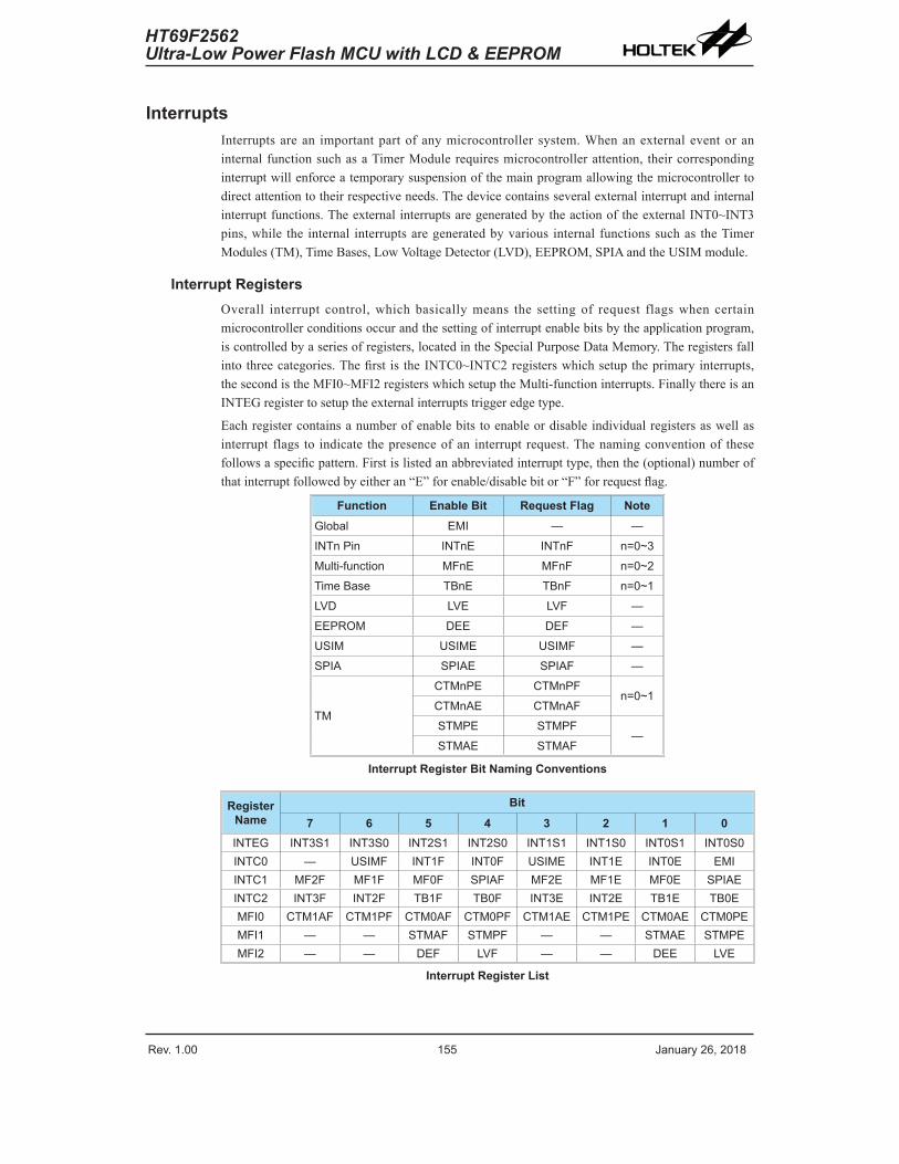
Rev. 1.00 154 ana 01 Rev. 1.00 155 ana 01
HT69F2562Ultra-Low Power Flash MCU with LCD & EEPROM
HT69F2562Ultra-Low Power Flash MCU with LCD & EEPROM
InterruptsInterruptsarean importantpartofanymicrocontroller system.WhenanexternaleventoraninternalfunctionsuchasaTimerModulerequiresmicrocontrollerattention, theircorrespondinginterruptwillenforceatemporarysuspensionofthemainprogramallowingthemicrocontrollertodirectattentiontotheirrespectiveneeds.Thedevicecontainsseveralexternalinterruptandinternalinterruptfunctions.TheexternalinterruptsaregeneratedbytheactionoftheexternalINT0~INT3pins,while the internal interruptsaregeneratedbyvarious internal functionssuchas theTimerModules(TM),TimeBases,LowVoltageDetector(LVD),EEPROM,SPIAandtheUSIMmodule.
Interrupt RegistersOverall interrupt control,whichbasicallymeans the settingof request flagswhen certainmicrocontrollerconditionsoccurandthesettingofinterruptenablebitsbytheapplicationprogram,iscontrolledbyaseriesofregisters,locatedintheSpecialPurposeDataMemory.Theregistersfallintothreecategories.Thefirst is theINTC0~INTC2registerswhichsetuptheprimaryinterrupts,thesecondistheMFI0~MFI2registerswhichsetuptheMulti-functioninterrupts.FinallythereisanINTEGregistertosetuptheexternalinterruptstriggeredgetype.
Eachregistercontainsanumberofenablebitstoenableordisableindividualregistersaswellasinterrupt flags to indicate thepresenceofan interrupt request.Thenamingconventionof thesefollowsaspecificpattern.Firstislistedanabbreviatedinterrupttype,thenthe(optional)numberofthatinterruptfollowedbyeitheran“E”forenable/disablebitor“F”forrequestflag.
Function Enable Bit Request Flag NoteGlobal EMI — —
INTn Pin INTnE INTnF n=0~3
Mlti-fnction MFnE MFnF n=0~
Time Base TBnE TBnF n=0~1
LVD LVE LVF —
EEPROM DEE DEF —
USIM USIME USIMF —
SPIA SPIAE SPIAF —
TM
CTMnPE CTMnPFn=0~1
CTMnAE CTMnAF
STMPE STMPF—
STMAE STMAF
Interrupt Register Bit Naming Conventions
Register Name
Bit
7 6 5 4 3 2 1 0INTEG INT3S1 INT3S0 INTS1 INTS0 INT1S1 INT1S0 INT0S1 INT0S0INTC0 — USIMF INT1F INT0F USIME INT1E INT0E EMIINTC1 MFF MF1F MF0F SPIAF MFE MF1E MF0E SPIAEINTC INT3F INTF TB1F TB0F INT3E INTE TB1E TB0EMFI0 CTM1AF CTM1PF CTM0AF CTM0PF CTM1AE CTM1PE CTM0AE CTM0PEMFI1 — — STMAF STMPF — — STMAE STMPEMFI — — DEF LVF — — DEE LVE
Interrupt Register List

Rev. 1.00 15 ana 01 Rev. 1.00 157 ana 01
HT69F2562Ultra-Low Power Flash MCU with LCD & EEPROM
HT69F2562Ultra-Low Power Flash MCU with LCD & EEPROM
• INTEG Register
Bit 7 6 5 4 3 2 1 0Name INT3S1 INT3S0 INTS1 INTS0 INT1S1 INT1S0 INT0S1 INT0S0R/W R/W R/W R/W R/W R/W R/W R/W R/WPOR 0 0 0 0 0 0 0 0
Bit7~6 INT3S1~INT3S0:InterruptEdgeControlforINT3Pin00:Disable01:Risingedge10:Fallingedge11:Risingandfallingedges
Bit5~4 INT2S1~INT2S0:InterruptEdgeControlforINT2Pin00:Disable01:Risingedge10:Fallingedge11:Risingandfallingedges
Bit3~2 INT1S1~INT1S0:InterruptEdgeControlforINT1Pin00:Disable01:Risingedge10:Fallingedge11:Risingandfallingedges
Bit1~0 INT0S1~INT0S0:InterruptEdgeControlforINT0Pin00:Disable01:Risingedge10:Fallingedge11:Risingandfallingedges
• INTC0 Register
Bit 7 6 5 4 3 2 1 0Name — USIMF INT1F INT0F USIME INT1E INT0E EMIR/W — R/W R/W R/W R/W R/W R/W R/WPOR — 0 0 0 0 0 0 0
Bit7 Unimplemented,readas“0”Bit6 USIMF:USIMInterruptRequestFlag
0:Norequest1:Interruptrequest
Bit5 INT1F:ExternalInterrupt1RequestFlag0:Norequest1:Interruptrequest
Bit4 INT0F:ExternalInterrupt0RequestFlag0:Norequest1:Interruptrequest
Bit3 USIME:USIMInterruptControl0:Disable1:Enable
Bit2 INT1E:ExternalInterrupt1Control0:Disable1:Enable
Bit1 INT0E:ExternalInterrupt0Control0:Disable1:Enable
Bit0 EMI:GlobalInterruptControl0:Disable1:Enable

Rev. 1.00 15 ana 01 Rev. 1.00 157 ana 01
HT69F2562Ultra-Low Power Flash MCU with LCD & EEPROM
HT69F2562Ultra-Low Power Flash MCU with LCD & EEPROM
• INTC1 Register
Bit 7 6 5 4 3 2 1 0Name MFF MF1F MF0F SPIAF MFE MF1E MF0E SPIAER/W R/W R/W R/W R/W R/W R/W R/W R/WPOR 0 0 0 0 0 0 0 0
Bit7 MF2F:Multi-functionInterrupt2RequestFlag0:Norequest1:Interruptrequest
Bit6 MF1F:Multi-functionInterrupt1RequestFlag0:Norequest1:Interruptrequest
Bit5 MF0F:Multi-functionInterrupt0RequestFlag0:Norequest1:Interruptrequest
Bit4 SPIAF:SPIAInterruptRequestFlag0:Norequest1:Interruptrequest
Bit3 MF2E:Multi-functionInterrupt2Control0:Disable1:Enable
Bit2 MF1E:Multi-functionInterrupt1Control0:Disable1:Enable
Bit1 MF0E:Multi-functionInterrupt0Control0:Disable1:Enable
Bit0 SPIAE:SPIAInterruptControl0:Disable1:Enable
• INTC2 Register
Bit 7 6 5 4 3 2 1 0Name INT3F INTF TB1F TB0F INT3E INTE TB1E TB0ER/W R/W R/W R/W R/W R/W R/W R/W R/WPOR 0 0 0 0 0 0 0 0
Bit7 INT3F:ExternalInterrupt3RequestFlag0:Norequest1:Interruptrequest
Bit6 INT2F:ExternalInterrupt2RequestFlag0:Norequest1:Interruptrequest
Bit5 TB1F:TimeBase1InterruptRequestFlag0:Norequest1:Interruptrequest
Bit4 TB0F:TimeBase0InterruptRequestFlag0:Norequest1:Interruptrequest
Bit3 INT3E:ExternalInterrupt3Control0:Disable1:Enable

Rev. 1.00 15 ana 01 Rev. 1.00 159 ana 01
HT69F2562Ultra-Low Power Flash MCU with LCD & EEPROM
HT69F2562Ultra-Low Power Flash MCU with LCD & EEPROM
Bit2 INT2E:ExternalInterrupt2Control0:Disable1:Enable
Bit1 TB1E:TimeBase1InterruptControl0:Disable1:Enable
Bit0 TB0E:TimeBase0InterruptControl0:Disable1:Enable
• MFI0 Register
Bit 7 6 5 4 3 2 1 0Name CTM1AF CTM1PF CTM0AF CTM0PF CTM1AE CTM1PE CTM0AE CTM0PER/W R/W R/W R/W R/W R/W R/W R/W R/WPOR 0 0 0 0 0 0 0 0
Bit7 CTM1AF:CTM1ComparatorAmatchinterruptrequestflag0:Norequest1:Interruptrequest
Bit6 CTM1PF:CTM1ComparatorPmatchinterruptrequestflag0:Norequest1:Interruptrequest
Bit5 CTM0AF:CTM0ComparatorAmatchinterruptrequestflag0:Norequest1:Interruptrequest
Bit4 CTM0PF:CTM0ComparatorPmatchinterruptrequestflag0:Norequest1:Interruptrequest
Bit3 CTM1AE:CTM1ComparatorAmatchinterruptcontrol0:Disable1:Enable
Bit2 CTM1PE:CTM1ComparatorPmatchinterruptcontrol0:Disable1:Enable
Bit1 CTM0AE:CTM0ComparatorAmatchinterruptcontrol0:Disable1:Enable
Bit0 CTM0PE:CTM0ComparatorPmatchinterruptcontrol0:Disable1:Enable

Rev. 1.00 15 ana 01 Rev. 1.00 159 ana 01
HT69F2562Ultra-Low Power Flash MCU with LCD & EEPROM
HT69F2562Ultra-Low Power Flash MCU with LCD & EEPROM
• MFI1 Register
Bit 7 6 5 4 3 2 1 0Name — — STMAF STMPF — — STMAE STMPER/W — — R/W R/W — — R/W R/WPOR — — 0 0 — — 0 0
Bit7~6 Unimplemented,readas“0”Bit5 STMAF:STMComparatorAmatchinterruptrequestflag
0:Norequest1:Interruptrequest
Bit4 STMPF:STMComparatorPmatchinterruptrequestflag0:Norequest1:Interruptrequest
Bit3~2 Unimplemented,readas“0”Bit1 STMAE:STMComparatorAmatchinterruptcontrol
0:Disable1:Enable
Bit0 STMPE:STMComparatorPmatchinterruptcontrol0:Disable1:Enable
• MFI2 Register
Bit 7 6 5 4 3 2 1 0Name — — DEF LVF — — DEE LVER/W — — R/W R/W — — R/W R/WPOR — — 0 0 — — 0 0
Bit7~6 Unimplemented,readas“0”Bit5 DEF:DataEEPROMinterruptrequestflag
0:Norequest1:Interruptrequest
Bit4 LVF:LVDinterruptrequestflag0:Norequest1:Interruptrequest
Bit3~2 Unimplemented,readas“0”Bit1 DEE:DataEEPROMinterruptcontrol
0:Disable1:Enable
Bit0 LVE:LVDinterruptcontrol0:Disable1:Enable
Interrupt OperationWhentheconditionsforaninterrupteventoccur,suchasaTMComparatorP,ComparatorAmatchoranEEPROMWritecycleendsetc., therelevantinterruptrequestflagwillbeset.Whethertherequestflagactuallygeneratesaprogramjumpto therelevant interruptvector isdeterminedbytheconditionoftheinterruptenablebit.Iftheenablebitissethighthentheprogramwilljumptoitsrelevantvector;iftheenablebitiszerothenalthoughtheinterruptrequestflagissetanactualinterruptwillnotbegeneratedandtheprogramwillnotjumptotherelevantinterruptvector.Theglobalinterruptenablebit,ifclearedtozero,willdisableallinterrupts.

Rev. 1.00 10 ana 01 Rev. 1.00 11 ana 01
HT69F2562Ultra-Low Power Flash MCU with LCD & EEPROM
HT69F2562Ultra-Low Power Flash MCU with LCD & EEPROM
Whenaninterruptisgenerated,theProgramCounter,whichstorestheaddressofthenextinstructiontobeexecuted,willbetransferredontothestack.TheProgramCounterwillthenbeloadedwithanewaddresswhichwillbethevalueofthecorrespondinginterruptvector.Themicrocontrollerwillthenfetchitsnextinstructionfromthisinterruptvector.Theinstructionatthisvectorwillusuallybea“JMP”whichwilljumptoanothersectionofprogramwhichisknownastheinterruptserviceroutine.Hereislocatedthecodetocontroltheappropriateinterrupt.Theinterruptserviceroutinemustbe terminatedwitha“RETI”,whichretrieves theoriginalProgramCounteraddressfromthestackandallowsthemicrocontrollertocontinuewithnormalexecutionatthepointwheretheinterruptoccurred.
Thevarious interruptenablebits, togetherwith theirassociatedrequest flags,areshownin theaccompanyingdiagramswith theirorderofpriority.Some interrupt sourceshave theirownindividualvectorwhileothersshare thesamemulti-function interruptvector.Oncean interruptsubroutineisserviced,all theother interruptswillbeblocked,as theglobal interruptenablebit,EMIbitwillbeclearedautomatically.Thiswillpreventanyfurtherinterruptnestingfromoccurring.However, ifother interruptrequestsoccurduringthis interval,althoughtheinterruptwillnotbeimmediatelyserviced,therequestflagwillstillberecorded.
Ifaninterruptrequiresimmediateservicingwhiletheprogramisalreadyinanotherinterruptserviceroutine,theEMIbitshouldbesetafterenteringtheroutine,toallowinterruptnesting.Ifthestackisfull,theinterruptrequestwillnotbeacknowledged,eveniftherelatedinterruptisenabled,untiltheStackPointerisdecremented.Ifimmediateserviceisdesired,thestackmustbepreventedfrombecomingfull.Incaseofsimultaneousrequests,theaccompanyingdiagramshowstheprioritythatisapplied.Alloftheinterruptrequestflagswhensetwillwake-upthedeviceifit isinSLEEPorIDLEMode,however topreventawake-upfromoccurringthecorrespondingflagshouldbesetbeforethedeviceisinSLEEPorIDLEMode.
Interrupt Name
Request Flags
Enable Bits
Master Enable Vector
EMI auto disabled in ISR
PriorityHigh
Low
Interrupts contained within Multi-Function Interrupts
xxE Enable Bits
xxF Request Flag, auto reset in ISR
LegendxxF Request Flag, no auto reset in ISR
INT2 Pin INT2F INT2E EMI
EMIINT3 Pin INT3F INT3E
28H
2CH
CTM1 P CTM1PF CTM1PE
04HINT0 Pin INT0F INT0E EMI
1CHM. Funct. 2 MF2F MF2E EMI
EMI 08HINT1 Pin INT1F INT1EInterrupt Name
Request Flags
Enable Bits
EMI 0CHUSIM Module USIMF USIME
EMI 10HSPIA SPIAF SPIAE
EMI 14HM. Funct. 0 MF0F MF0E
24HTime Base 1 TB1F TB1E EMI
CTM1 A CTM1AF CTM1AE
EEPROM DEE DEF
LVD LVF LVE
18HM. Funct. 1 MF1F MF1E EMI
20HTime Base 0 TB0F TB0E EMI
CTM0 P CTM0PF CTM0PE
CTM0 A CTM0AF CTM0AE
STM P STMPF STMPE
STM A STMAF STMAE
Interrupt Structure

Rev. 1.00 10 ana 01 Rev. 1.00 11 ana 01
HT69F2562Ultra-Low Power Flash MCU with LCD & EEPROM
HT69F2562Ultra-Low Power Flash MCU with LCD & EEPROM
External InterruptTheexternal interruptsarecontrolledbysignal transitionsonthepinsINT0~INT3.Anexternalinterruptrequestwill takeplacewhentheexternalinterruptrequestflags,INT0F~INT3F,areset,whichwilloccurwhenatransition,whosetypeischosenbytheedgeselectbits,appearsontheexternal interruptpins.Toallowtheprogramtobranchtoitsrespectiveinterruptvectoraddress,theglobal interruptenablebit,EMI,andrespectiveexternal interruptenablebit, INT0E~INT3E,mustfirstbeset.Additionally thecorrect interruptedgetypemustbeselectedusingtheINTEGregistertoenabletheexternalinterruptfunctionandtochoosethetriggeredgetype.Astheexternalinterruptpinsarepin-sharedwithI/Opins,theycanonlybeconfiguredasexternalinterruptpinsiftheirexternalinterruptenablebitinthecorrespondinginterruptregisterhasbeensetandtheexternalinterruptpinisselectedbythecorrespondingpin-sharedfunctionselectionbits.Thepinmustalsobesetupasaninputbysettingthecorrespondingbitintheportcontrolregister.
Whentheinterrupt isenabled, thestackisnotfullandthecorrect transitiontypeappearsontheexternalinterruptpin,asubroutinecall totheexternalinterruptvector,will takeplace.Whentheinterrupt isserviced, theexternal interrupt request flags, INT0F~INT3F,willbeautomaticallyresetandtheEMIbitwillbeautomaticallyclearedtodisableotherinterrupts.Notethatanypull-highresistorselectionsontheexternalinterruptpinswillremainvalidevenifthepinisusedasanexternalinterruptinput.TheINTEGregisterisusedtoselectthetypeofactiveedgethatwilltriggertheexternalinterrupt.Achoiceofeitherrisingorfallingorbothedgetypescanbechosentotriggeranexternalinterrupt.NotethattheINTEGregistercanalsobeusedtodisabletheexternalinterruptfunction.
Multi-function InterruptWithin thedevice there are severalMulti-function interrupts.Unlike theother independentinterrupts, theseinterruptshavenoindependentsource,butratherareformedfromotherexistinginterruptsources,namelytheTMinterrupts,LVDinterrupandEEPROMwriteoperationinterrupt.
AMulti-functioninterruptrequestwilltakeplacewhenanyoftheMulti-functioninterruptrequestflagsMFnFareset.TheMulti-function interrupt flagswillbesetwhenanyof their includedfunctionsgenerateaninterruptrequestflag.Toallowtheprogramtobranchtoitsrespectiveinterruptvectoraddress,whentheMulti-functioninterruptisenabledandthestackisnotfull,andeitheroneoftheinterruptscontainedwithineachofMulti-functioninterruptoccurs,asubroutinecalltooneoftheMulti-functioninterruptvectorswilltakeplace.Whentheinterruptisserviced,therelatedMulti-FunctionrequestflagwillbeautomaticallyresetandtheEMIbitwillbeautomaticallyclearedtodisableotherinterrupts.
However, itmustbenoted that, although theMulti-function Interrupt request flagswill beautomaticallyresetwhen the interrupt isserviced, therequest flagsfromtheoriginalsourceoftheMulti-function interruptswillnotbeautomaticallyresetandmustbemanuallyresetby theapplicationprogram.
Timer Module InterruptsTheCompactandStandardtypeTMseachhastwointerrupts,onecomesfromthecomparatorAmatchsituationandtheothercomesfromthecomparatorPmatchsituation.AlloftheTMinterruptsarecontainedwithintheMulti-functionInterrupts.ForalloftheTMtypestherearetwointerruptrequestflagsandtwoenablecontrolbits.ATMinterruptrequestwill takeplacewhenanyoftheTMrequestflagsareset,asituationwhichoccurswhenaTMcomparatorPorAmatchsituationhappens.

Rev. 1.00 1 ana 01 Rev. 1.00 13 ana 01
HT69F2562Ultra-Low Power Flash MCU with LCD & EEPROM
HT69F2562Ultra-Low Power Flash MCU with LCD & EEPROM
Toallowtheprogramtobranchtoitsrespectiveinterruptvectoraddress,theglobalinterruptenablebit,EMI,respectiveTMInterruptenablebit,andrelevantMulti-functionInterruptenablebit,MFnE,mustfirstbeset.Whentheinterruptisenabled,thestackisnotfullandaTMcomparatormatchsituationoccurs,asubroutinecalltotherelevantMulti-functionInterruptvectorlocations,willtakeplace.WhentheTMinterruptisserviced,theEMIbitwillbeautomaticallyclearedtodisableotherinterrupts.However,onlytherelatedMFnFflagwillbeautomaticallycleared.AstheTMinterruptrequestflagswillnotbeautomaticallycleared,theyhavetobeclearedbytheapplicationprogram.
LVD InterruptTheLowVoltageDetector Interrupt iscontainedwithin theMulti-function Interrupt.AnLVDInterruptrequestwill takeplacewhentheLVDInterruptrequest flag,LVF, isset,whichoccurswhentheLowVoltageDetectorfunctiondetectsalowpowersupplyvoltage.Toallowtheprogramtobranchtoitsrespectiveinterruptvectoraddress,theglobalinterruptenablebit,EMI,LowVoltageInterruptenablebit,LVE,andassociatedMulti-functioninterruptenablebit,mustfirstbeset.Whentheinterruptisenabled,thestackisnotfullandalowvoltageconditionoccurs,asubroutinecalltotheMulti-functionInterruptvector,willtakeplace.WhentheLowVoltageInterruptisserviced,theEMIbitwillbeautomaticallyclearedtodisableotherinterrupts,howeveronlytheMulti-functioninterruptrequestflagwillbealsoautomaticallycleared.AstheLVFflagwillnotbeautomaticallycleared,ithastobeclearedbytheapplicationprogram.
EEPROM InterruptTheEEPROMInterrupt iscontainedwithin theMulti-functionInterrupt.AnEEPROMInterruptrequestwill takeplacewhen theEEPROMInterrupt request flag,DEF, is set,whichoccurswhenanEEPROMWritecycleends.Toallowtheprogramtobranchto itsrespectiveinterruptvectoraddress,theglobalinterruptenablebit,EMI,andEEPROMInterruptenablebit,DEE,andassociatedMulti-functioninterruptenablebit,mustfirstbeset.Whentheinterruptisenabled,thestackisnotfullandanEEPROMWritecycleends,asubroutinecall totherespectiveEEPROMInterruptvectorwill takeplace.When theEEPROMInterrupt isserviced, theEMIbitwillbeautomaticallyclearedtodisableotherinterrupts,howeveronlytheMulti-functioninterruptrequestflagwillbealsoautomaticallycleared.AstheDEFflagwillnotbeautomaticallycleared,ithastobeclearedbytheapplicationprogram.
USIM InterruptTheUniversalSerialInterfaceModuleInterrupt,alsoknownastheUSIMinterrupt,willtakeplacewhentheUSIMInterruptrequestflag,USIMF,isset.AstheUSIMinterfacecanoperateinthreemodeswhichareSPImode,I2CmodeandUARTmode, theUSIMFflagcanbesetbydifferentconditionsdependingontheselectedinterfacemode.
IftheSPIorI2Cmodeisselected,theUSIMinterruptcanbetriggeredwhenabyteofdatahasbeenreceivedortransmittedbytheUSIMSPIorI2Cinterface,oranI2Cslaveaddressmatchoccurs,oranI2Cbustime-outoccurs.IftheUARTmodeisselected,severalindividualUARTconditionsincludingatransmitterdataregisterempty,transmitteridle,receiverdataavailable,receiveroverrun,addressdetectandanRXpinwake-up,cangenerateaUSIMinterruptwiththeUSIMFflagbitsethigh.
Toallowtheprogramtobranchtoitsrespectiveinterruptvectoraddress,theglobalinterruptenablebit,EMI,andtheUniversalSerialInterfaceModuleInterruptenablebit,USIME,mustfirstbeset.Whentheinterruptisenabled,thestackisnotfullandanyoftheabovedescribedsituationsoccurs,asubroutinecalltotherespectiveInterruptvector,willtakeplace.Whentheinterruptisserviced,theUniversalSerialInterfaceModuleInterruptflag,USIMF,willbeautomaticallycleared.TheEMIbitwillalsobeautomaticallyclearedtodisableotherinterrupts.

Rev. 1.00 1 ana 01 Rev. 1.00 13 ana 01
HT69F2562Ultra-Low Power Flash MCU with LCD & EEPROM
HT69F2562Ultra-Low Power Flash MCU with LCD & EEPROM
Note that if theUSIMinterrupt is triggeredbytheUARTinterface,after the interrupthasbeenserviced,theUUSRregisterflagswillonlybeclearedwhencertainactionsaretakenbytheUART,thedetailsofwhicharegivenintheUARTsection.
SPIA Interface InterruptAnSPIAInterruptrequestwilltakeplacewhentheSPIAInterruptrequestflag,SPIAF,isset,whichoccurswhenabyteofdatahasbeenreceivedor transmittedbytheSPIAinterface.Toallowtheprogramtobranchtoitsrespectiveinterruptvectoraddress, theglobal interruptenablebit,EMI,andtheSerialInterfaceInterruptenablebit,SPIAE,mustfirstbeset.Whentheinterruptisenabled,thestackisnotfullandabyteofdatahasbeentransmittedorreceivedbytheSPIAinterface,asubroutinecalltotherespectiveInterruptvector,willtakeplace.WhentheSPIAInterfaceInterruptisserviced, theSPIAFflagwillbeautomaticallycleared, theEMIbitwillalsobeautomaticallyclearedtodisableotherinterrupts.
Time Base InterruptsThefunctionoftheTimeBaseInterruptsistoprovideregulartimesignalintheformofaninternalinterrupt.Theyarecontrolledbytheoverflowsignalsfromtheirrespectivetimerfunctions.Whenthesehappens their respective interrupt request flags,TB0ForTB1Fwillbeset.Toallowtheprogramtobranchtotheirrespectiveinterruptvectoraddresses,theglobalinterruptenablebit,EMI,andTimeBaseenablebits,TB0EorTB1E,mustfirstbeset.Whentheinterruptisenabled,thestackisnotfullandtheTimeBaseoverflows,asubroutinecall totheirrespectivevectorlocationswilltakeplace.Whentheinterruptisserviced,therespectiveinterruptrequestflag,TB0ForTB1F,willbeautomaticallycleared,theEMIbitwillalsobeautomaticallyclearedtodisableotherinterrupts.
ThepurposeoftheTimeBaseInterruptistoprovideaninterruptsignalatfixedtimeperiods.Itsclocksource,fPSC0orfPSC1,originatesfromtheinternalclocksourcefLXT/8andthenpassesthroughadivider,thedivisionratioofwhichisselectedbyprogrammingtheappropriatebitsintheTB0CandTB1Cregisterstoobtainlongerinterruptperiodswhosevalueranges.
Prescaler 0fPSC0 fPSC0/28 ~ fPSC0/215 M
UX
MUX
TB0[2:0]
TB1[2:0]
Time Base 0 Interrupt
Time Base 1 Interrupt
TB0ON
TB1ON
Prescaler 1fPSC1 fPSC1/28 ~ fPSC1/215
fLXT/8 PSC0EN
PSC1EN
Time Base Interrupts

Rev. 1.00 14 ana 01 Rev. 1.00 15 ana 01
HT69F2562Ultra-Low Power Flash MCU with LCD & EEPROM
HT69F2562Ultra-Low Power Flash MCU with LCD & EEPROM
• PSCnR Register (n=0~1)
Bit 7 6 5 4 3 2 1 0Name — — — — — — — PSCnENR/W — — — — — — — R/WPOR — — — — — — — 0
Bit7~1 Unimplemented,readas"0"Bit0 PSCnEN:Prescalernclockenablecontrol
0:Disable1:Enable
ThisPSCnENbitisthePrescalernclockenable/disablecontrolbit.WhenthePrescaleclockisdisabled,itcanreduceextrapowerconsumption.PrescalernclockissourcedfromtheLXToscillatoroutputfrequencyoffLXT/8.
• TB0C Register
Bit 7 6 5 4 3 2 1 0Name TB0ON — — — — TB0 TB01 TB00R/W R/W — — — — R/W R/W R/WPOR 0 — — — — 0 0 0
Bit7 TB0ON:TimeBase0Control0:Disable1:Enable
Bit6~3 Unimplemented,readas“0”Bit2~0 TB02~TB00:SelectTimeBase0Time-outPeriod
000:28/fPSC0001:29/fPSC0010:210/fPSC0011:211/fPSC0100:212/fPSC0101:213/fPSC0110:214/fPSC0111:215/fPSC0
• TB1C Register
Bit 7 6 5 4 3 2 1 0Name TB1ON — — — — TB1 TB11 TB10R/W R/W — — — — R/W R/W R/WPOR 0 — — — — 0 0 0
Bit7 TB1ON:TimeBase1Control0:Disable1:Enable
Bit6~3 Unimplemented,readas“0”Bit2~0 TB12~TB10:SelectTimeBase1Time-outPeriod
000:28/fPSC1001:29/fPSC1010:210/fPSC1011:211/fPSC1100:212/fPSC1101:213/fPSC1110:214/fPSC1111:215/fPSC1

Rev. 1.00 14 ana 01 Rev. 1.00 15 ana 01
HT69F2562Ultra-Low Power Flash MCU with LCD & EEPROM
HT69F2562Ultra-Low Power Flash MCU with LCD & EEPROM
Interrupt Wake-up FunctionEachof the interruptfunctionshas thecapabilityofwakingupthemicrocontrollerwhenin theSLEEPorIDLEMode.Awake-upisgeneratedwhenaninterruptrequestflagchangesfromlowtohighandisindependentofwhethertheinterruptisenabledornot.Therefore,eventhoughthedeviceisintheSLEEPorIDLEModeanditssystemoscillatorstopped,situationssuchasexternaledgetransitionsontheexternalinterruptpinsoralowpowersupplyvoltagemaycausetheirrespectiveinterruptflagtobesethighandconsequentlygenerateaninterrupt.Caremustthereforebetakenifspuriouswake-upsituationsaretobeavoided.Ifaninterruptwake-upfunctionistobedisabledthenthecorrespondinginterruptrequestflagshouldbesethighbeforethedeviceenterstheSLEEPorIDLEMode.Theinterruptenablebitshavenoeffectontheinterruptwake-upfunction.
Programming ConsiderationsBydisablingtherelevantinterruptenablebits,arequestedinterruptcanbepreventedfrombeingserviced,however,oncean interrupt request flag is set, itwill remain in thiscondition in theinterruptregisteruntilthecorrespondinginterruptisservicedoruntiltherequestflagisclearedbytheapplicationprogram.
Whereacertain interrupt iscontainedwithinaMulti-function interrupt, thenwhenthe interruptservice routine isexecuted,asonly theMulti-function interrupt request flags,MFnF,willbeautomaticallycleared, the individual request flag for the functionneeds tobeclearedby theapplicationprogram.
It isrecommendedthatprogramsdonotusethe“CALL”instructionwithintheinterruptservicesubroutine.Interruptsoftenoccurinanunpredictablemannerorneedtobeservicedimmediately.Ifonlyonestackisleftandtheinterruptisnotwellcontrolled,theoriginalcontrolsequencewillbedamagedonceaCALLsubroutineisexecutedintheinterruptsubroutine.
Everyinterrupthasthecapabilityofwakingupthemicrocontrollerwhenit isinSLEEPorIDLEMode,thewakeupbeinggeneratedwhentheinterruptrequestflagchangesfromlowtohigh.IfitisrequiredtopreventacertaininterruptfromwakingupthemicrocontrollerthenitsrespectiverequestflagshouldbefirstsethighbeforeenterSLEEPorIDLEMode.
AsonlytheProgramCounter ispushedontothestack, thenwhentheinterrupt isserviced, if thecontentsof theaccumulator,statusregisterorotherregistersarealteredbythe interruptserviceprogram,theircontentsshouldbesavedto thememoryat thebeginningof the interruptserviceroutine.Toreturnfromaninterruptsubroutine,eitheraRETorRETIinstructionmaybeexecuted.TheRETIinstructioninadditiontoexecutingareturntothemainprogramalsoautomaticallysetstheEMIbithightoallowfurtherinterrupts.TheRETinstructionhoweveronlyexecutesareturntothemainprogramleavingtheEMIbitinitspresentzerostateandthereforedisablingtheexecutionoffurtherinterrupts.

Rev. 1.00 1 ana 01 Rev. 1.00 17 ana 01
HT69F2562Ultra-Low Power Flash MCU with LCD & EEPROM
HT69F2562Ultra-Low Power Flash MCU with LCD & EEPROM
Low Voltage Detector – LVDThedevicehasaLowVoltageDetectorfunction,alsoknownasLVD.Thisenabledthedevicetomonitorthepowersupplyvoltage,VDD,andprovideawarningsignalshoulditfallbelowacertainlevel.Thisfunctionmaybeespeciallyusefulinbatteryapplicationswherethesupplyvoltagewillgraduallyreduceasthebatteryages,asitallowsanearlywarningbatterylowsignaltobegenerated.TheLowVoltageDetectoralsohasthecapabilityofgeneratinganinterruptsignal.
LVD RegisterTheLowVoltageDetectorfunctioniscontrolledusingasingleregisterwiththenameLVDC.Fourbitsinthisregister,VLVD3~VLVD0,areusedtoselectoneofsixteenfixedvoltagesbelowwhichalowvoltageconditionwillbedetermined.AlowvoltageconditionisindicatedwhentheLVDObitisset.IftheLVDObitislow,thisindicatesthattheVDDvoltageisabovethepresetlowvoltagevalue.TheLVDENbit isusedtocontrol theoverallon/offfunctionof thelowvoltagedetector.Settingthebithighwillenablethelowvoltagedetector.Clearingthebittozerowillswitchofftheinternallowvoltagedetectorcircuits.Asthelowvoltagedetectorwillconsumeacertainamountofpower,itmaybedesirabletoswitchoffthecircuitwhennotinuse,animportantconsiderationinpowersensitivebatterypoweredapplications.
• LVDC Register
Bit 7 6 5 4 3 2 1 0Name — — LVDO LVDEN VLVD3 VLVD VLVD1 VLVD0R/W — — R R/W R/W R/W R/W R/WPOR — — 0 0 0 0 0 0
Bit7~6 Unimplemented,readas“0”Bit5 LVDO:LVDOutputFlag
0:NoLowVoltageDetect1:LowVoltageDetect
Bit4 LVDEN:LowVoltageDetectorControl0:Disable1:Enable
Bit3~0 VLVD3~VLVD0:SelectLVDVoltage0000:1.8V0001:1.9V0010:2.0V0011:2.1V0100:2.2V0101:2.3V0110:2.4V0111:2.5V1000:2.6V1001:2.7V1010:2.8V1011:2.9V1100:3.0V1101:3.3V1110:3.6V1111:4.0V

Rev. 1.00 1 ana 01 Rev. 1.00 17 ana 01
HT69F2562Ultra-Low Power Flash MCU with LCD & EEPROM
HT69F2562Ultra-Low Power Flash MCU with LCD & EEPROM
LVD OperationTheLowVoltageDetectorfunctionoperatesbycomparingthepowersupplyvoltage,VDD,withapre-specifiedvoltagelevelstoredintheLVDCregister.Thishasarangeofbetween1.8Vand4.0V.Whenthepowersupplyvoltage,VDD,fallsbelowthispre-determinedvalue,theLVDObitwillbesethighindicatingalowpowersupplyvoltagecondition.WhenthedeviceisintheSLEEPmode,thelowvoltagedetectorwillbedisabledevenif theLVDENbit ishigh.AfterenablingtheLowVoltageDetector,atimedelaytLVDSshouldbeallowedforthecircuitrytostabilisebeforereadingtheLVDObit.NotealsothatastheVDDvoltagemayriseandfallratherslowly,atthevoltagenearsthatofVLVD,theremaybemultiplebitLVDOtransitions.
VDD
LVDEN
LVDO
VLVD
tLVDS
LVD Operation
TheLowVoltageDetectoralsohasitsowninterruptwhichiscontainedwithinoneoftheMulti-functioninterrupts,providinganalternativemeansoflowvoltagedetection,inadditiontopollingtheLVDObit.TheinterruptwillonlybegeneratedafteradelayoftLVDaftertheLVDObithasbeensethighbyalowvoltagecondition.Inthiscase,theLVFinterruptrequestflagwillbeset,causinganinterrupttobegeneratedifVDDfallsbelowthepresetLVDvoltage.Thiswillcausethedevicetowake-upfromtheIDLEMode,however if theLowVoltageDetectorwakeupfunctionisnotrequiredthentheLVFflagshouldbefirstsethighbeforethedeviceenterstheIDLEMode.
Configuration OptionsConfigurationoptionsrefertocertainoptionswithintheMCUthatareprogrammedintothedeviceduringtheprogrammingprocess.Duringthedevelopmentprocess,theseoptionsareselectedusingtheHT-IDEsoftwaredevelopment tools.Astheseoptionsareprogrammedintothedeviceusingthehardwareprogrammingtools,once theyareselectedtheycannotbechangedlaterusingtheapplicationprogram.Alloptionsmustbedefinedforpropersystemfunction,thedetailsofwhichareshowninthetable.
No. Options
1
HIRC feqenc selection:1. 4MHz. MHz3. 1MHz
Note:When theHIRChasbeenconfiguredata frequencyshownin this table, theHIRC1andHIRC0bitsshouldalsobesetuptoselectthesamefrequencytoachievetheHIRCfrequencyaccuracyspecifiedintheA.C.Characteristics.

Rev. 1.00 1 ana 01 Rev. 1.00 19 ana 01
HT69F2562Ultra-Low Power Flash MCU with LCD & EEPROM
HT69F2562Ultra-Low Power Flash MCU with LCD & EEPROM
Application Circuits
LCD Power Source from External
PA0~7
XT1
XT2
VDD
VSS
RES
VDD
LCDPanel
COM0~COM3
C1
C2
V1
32768Hz
C1
C2
V2
SEG0~SEG31
LCD Power source
PLCD
PB0~7
Key Matrix Input
PC0~3
I2CSPIUART
VMAX LCD maximum voltage
100kΩ
0.1μF
0.1μF
0.1μF
0.1μF
0.1μF
LCD Power Source from Internal Regulator
XT1
XT2
VDD
VSS
100kΩ
0.1μF
0.1μF RES
VDD
LCDPanel
COM0~COM3
C1
C2
V1
32768Hz
C1
C2
V2
SEG0~SEG31
0.1μF
0.1μF
0.1μF
PLCD
Key Matrix Input
0.1μF
PA0~7PB0~7PC0~3
I2CSPIUART
VMAX LCD maximum voltage

Rev. 1.00 1 ana 01 Rev. 1.00 19 ana 01
HT69F2562Ultra-Low Power Flash MCU with LCD & EEPROM
HT69F2562Ultra-Low Power Flash MCU with LCD & EEPROM
Instruction Set
IntroductionCentral to thesuccessfuloperationofanymicrocontroller is its instructionset,whichisasetofprograminstructioncodesthatdirectsthemicrocontrollertoperformcertainoperations.InthecaseofHoltekmicrocontroller,acomprehensiveandflexiblesetofover60instructionsisprovidedtoenableprogrammerstoimplementtheirapplicationwiththeminimumofprogrammingoverheads.
Foreasierunderstandingofthevariousinstructioncodes, theyhavebeensubdividedintoseveralfunctionalgroupings.
Instruction TimingMostinstructionsareimplementedwithinoneinstructioncycle.Theexceptionstothisarebranch,call,or tablereadinstructionswheretwoinstructioncyclesarerequired.Oneinstructioncycleisequalto4systemclockcycles,thereforeinthecaseofan8MHzsystemoscillator,mostinstructionswouldbeimplementedwithin0.5μsandbranchorcall instructionswouldbeimplementedwithin1μs.Although instructionswhichrequireonemorecycle to implementaregenerally limited totheJMP,CALL,RET,RETIandtablereadinstructions, it is important torealize thatanyotherinstructionswhichinvolvemanipulationoftheProgramCounterLowregisterorPCLwillalsotakeonemorecycletoimplement.AsinstructionswhichchangethecontentsofthePCLwill implyadirect jumptothatnewaddress,onemorecyclewillberequired.Examplesofsuchinstructionswouldbe“CLRPCL”or“MOVPCL,A”.Forthecaseofskipinstructions,itmustbenotedthatiftheresultofthecomparisoninvolvesaskipoperationthenthiswillalsotakeonemorecycle,ifnoskipisinvolvedthenonlyonecycleisrequired.
Moving and Transferring DataThe transferofdatawithin themicrocontrollerprogram isoneof themost frequentlyusedoperations.MakinguseofseveralkindsofMOVinstructions,datacanbetransferredfromregisterstotheAccumulatorandvice-versaaswellasbeingabletomovespecificimmediatedatadirectlyintotheAccumulator.Oneofthemostimportantdatatransferapplicationsistoreceivedatafromtheinputportsandtransferdatatotheoutputports.
Arithmetic OperationsTheabilitytoperformcertainarithmeticoperationsanddatamanipulationisanecessaryfeatureofmostmicrocontrollerapplications.WithintheHoltekmicrocontrollerinstructionsetarearangeofaddandsubtract instructionmnemonicstoenablethenecessaryarithmetictobecarriedout.Caremustbe taken toensurecorrecthandlingofcarryandborrowdatawhenresultsexceed255foradditionandless than0forsubtraction.Theincrementanddecrement instructionssuchasINC,INCA,DECandDECAprovideasimplemeansofincreasingordecreasingbyavalueofoneofthevaluesinthedestinationspecified.

Rev. 1.00 170 ana 01 Rev. 1.00 171 ana 01
HT69F2562Ultra-Low Power Flash MCU with LCD & EEPROM
HT69F2562Ultra-Low Power Flash MCU with LCD & EEPROM
Logical and Rotate OperationThestandardlogicaloperationssuchasAND,OR,XORandCPLallhavetheirowninstructionwithintheHoltekmicrocontroller instructionset.Aswiththecaseofmost instructionsinvolvingdatamanipulation, datamust pass through theAccumulatorwhichmay involve additionalprogrammingsteps. Inall logicaldataoperations, thezero flagmaybeset if the resultof theoperationiszero.AnotherformoflogicaldatamanipulationcomesfromtherotateinstructionssuchasRR,RL,RRCandRLCwhichprovideasimplemeansofrotatingonebitrightorleft.Differentrotateinstructionsexistdependingonprogramrequirements.Rotateinstructionsareusefulforserialportprogrammingapplicationswheredatacanberotatedfromaninternalregister intotheCarrybitfromwhereitcanbeexaminedandthenecessaryserialbitsethighorlow.Anotherapplicationwhichrotatedataoperationsareusedistoimplementmultiplicationanddivisioncalculations.
Branches and Control TransferProgrambranchingtakestheformofeitherjumpstospecifiedlocationsusingtheJMPinstructionor toa subroutineusing theCALL instruction.Theydiffer in the sense that in thecaseofasubroutinecall, theprogrammustreturn to the instruction immediatelywhenthesubroutinehasbeencarriedout.Thisisdonebyplacingareturninstruction“RET”inthesubroutinewhichwillcausetheprogramtojumpbacktotheaddressrightaftertheCALLinstruction.InthecaseofaJMPinstruction,theprogramsimplyjumpstothedesiredlocation.ThereisnorequirementtojumpbacktotheoriginaljumpingoffpointasinthecaseoftheCALLinstruction.Onespecialandextremelyusefulsetofbranchinstructionsaretheconditionalbranches.Hereadecisionisfirstmaderegardingtheconditionofacertaindatamemoryor individualbits.Dependingupon theconditions, theprogramwillcontinuewiththenextinstructionorskipoveritandjumptothefollowinginstruction.These instructionsare thekey todecisionmakingandbranchingwithin theprogramperhapsdeterminedbytheconditionofcertaininputswitchesorbytheconditionofinternaldatabits.
Bit OperationsTheabilitytoprovidesinglebitoperationsonDataMemoryisanextremelyflexiblefeatureofallHoltekmicrocontrollers.Thisfeature isespeciallyusefulforoutputportbitprogrammingwhereindividualbitsorportpinscanbedirectlysethighorlowusingeitherthe“SET[m].i”or“CLR[m].i”instructionsrespectively.Thefeatureremovestheneedforprogrammerstofirstreadthe8-bitoutputport,manipulatetheinputdatatoensurethatotherbitsarenotchangedandthenoutputtheportwiththecorrectnewdata.Thisread-modify-writeprocessistakencareofautomaticallywhenthesebitoperationinstructionsareused.
Table Read OperationsDatastorage isnormally implementedbyusing registers.However,whenworkingwith largeamountsoffixeddata, thevolumeinvolvedoftenmakesit inconvenienttostorethefixeddataintheDataMemory.Toovercomethisproblem,HoltekmicrocontrollersallowanareaofProgramMemorytobesetupasatablewheredatacanbedirectlystored.Asetofeasytouseinstructionsprovides themeansbywhich this fixeddatacanbereferencedandretrievedfromtheProgramMemory.
Other OperationsInaddition to theabovefunctional instructions,a rangeofother instructionsalsoexistsuchasthe“HALT”instructionforPower-downoperationsand instructions tocontrol theoperationoftheWatchdogTimerfor reliableprogramoperationsunderextremeelectricorelectromagneticenvironments.Fortheirrelevantoperations,refertothefunctionalrelatedsections.

Rev. 1.00 170 ana 01 Rev. 1.00 171 ana 01
HT69F2562Ultra-Low Power Flash MCU with LCD & EEPROM
HT69F2562Ultra-Low Power Flash MCU with LCD & EEPROM
Instruction Set SummaryTheinstructionsrelated to thedatamemoryaccess in thefollowingtablecanbeusedwhenthedesireddatamemoryislocatedinDataMemorysector0.
Table Conventionsx:Bitsimmediatedatam:DataMemoryaddressA:Accumulatori:0~7numberofbitsaddr:Programmemoryaddress
Mnemonic Description Cycles Flag AffectedArithmeticADD A[m] Add Data Memo to ACC 1 Z C AC OV SCADDM A[m] Add ACC to Data Memo 1Note Z C AC OV SCADD Ax Add immediate data to ACC 1 Z C AC OV SCADC A[m] Add Data Memo to ACC with Ca 1 Z C AC OV SCADCM A[m] Add ACC to Data memo with Ca 1Note Z C AC OV SCSUB Ax Sbtact immediate data fom the ACC 1 Z C AC OV SC CZSUB A[m] Sbtact Data Memo fom ACC 1 Z C AC OV SC CZSUBM A[m] Sbtact Data Memo fom ACC with eslt in Data Memo 1Note Z C AC OV SC CZSBC Ax Sbtact immediate data fom ACC with Ca 1 Z C AC OV SC CZSBC A[m] Sbtact Data Memo fom ACC with Ca 1 Z C AC OV SC CZSBCM A[m] Sbtact Data Memo fom ACC with Ca eslt in Data Memo 1Note Z C AC OV SC CZDAA [m] Decimal adjst ACC fo Addition with eslt in Data Memo 1Note CLogic OperationAND A[m] Logical AND Data Memo to ACC 1 ZOR A[m] Logical OR Data Memo to ACC 1 ZXOR A[m] Logical XOR Data Memo to ACC 1 ZANDM A[m] Logical AND ACC to Data Memo 1Note ZORM A[m] Logical OR ACC to Data Memo 1Note ZXORM A[m] Logical XOR ACC to Data Memo 1Note ZAND Ax Logical AND immediate Data to ACC 1 ZOR Ax Logical OR immediate Data to ACC 1 ZXOR Ax Logical XOR immediate Data to ACC 1 ZCPL [m] Complement Data Memo 1Note ZCPLA [m] Complement Data Memo with eslt in ACC 1 ZIncrement & DecrementINCA [m] Incement Data Memo with eslt in ACC 1 ZINC [m] Incement Data Memo 1Note ZDECA [m] Decement Data Memo with eslt in ACC 1 ZDEC [m] Decement Data Memo 1Note ZRotateRRA [m] Rotate Data Memo ight with eslt in ACC 1 NoneRR [m] Rotate Data Memo ight 1Note NoneRRCA [m] Rotate Data Memo ight thogh Ca with eslt in ACC 1 CRRC [m] Rotate Data Memo ight thogh Ca 1Note CRLA [m] Rotate Data Memo left with eslt in ACC 1 NoneRL [m] Rotate Data Memo left 1Note NoneRLCA [m] Rotate Data Memo left thogh Ca with eslt in ACC 1 CRLC [m] Rotate Data Memo left thogh Ca 1Note C

Rev. 1.00 17 ana 01 Rev. 1.00 173 ana 01
HT69F2562Ultra-Low Power Flash MCU with LCD & EEPROM
HT69F2562Ultra-Low Power Flash MCU with LCD & EEPROM
Mnemonic Description Cycles Flag AffectedData MoveMOV A[m] Move Data Memo to ACC 1 NoneMOV [m]A Move ACC to Data Memo 1Note NoneMOV Ax Move immediate data to ACC 1 NoneBit OperationCLR [m].i Clea bit of Data Memo 1Note NoneSET [m].i Set bit of Data Memo 1Note NoneBranch OperationMP add mp nconditionall NoneSZ [m] Skip if Data Memo is zeo 1Note NoneSZA [m] Skip if Data Memo is zeo with data movement to ACC 1Note NoneSZ [m].i Skip if bit i of Data Memo is zeo 1Note NoneSNZ [m] Skip if Data Memo is not zeo 1Note NoneSNZ [m].i Skip if bit i of Data Memo is not zeo 1Note NoneSIZ [m] Skip if incement Data Memo is zeo 1Note NoneSDZ [m] Skip if decement Data Memo is zeo 1Note NoneSIZA [m] Skip if incement Data Memo is zeo with eslt in ACC 1Note NoneSDZA [m] Skip if decement Data Memo is zeo with eslt in ACC 1Note NoneCALL add Sbotine call NoneRET Retn fom sbotine NoneRET Ax Retn fom sbotine and load immediate data to ACC NoneRETI Retn fom intept NoneTable Read OperationTABRD [m] Read table (specific page) to TBLH and Data Memory Note NoneTABRDL [m] Read table (last page) to TBLH and Data Memo Note NoneITABRD [m] Increment table pointer TBLP first and Read table to TBLH and Data Memory Note None
ITABRDL [m] Increment table pointer TBLP first and Read table (last page) to TBLH and Data Memo Note None
MiscellaneousNOP No opeation 1 NoneCLR [m] Clea Data Memo 1Note NoneSET [m] Set Data Memo 1Note NoneCLR WDT Clea Watchdog Time 1 TO PDFSWAP [m] Swap nibbles of Data Memo 1Note NoneSWAPA [m] Swap nibbles of Data Memo with eslt in ACC 1 NoneHALT Ente powe down mode 1 TO PDF
Note:1.Forskipinstructions,iftheresultofthecomparisoninvolvesaskipthenuptothreecyclesarerequired,ifnoskiptakesplaceonlyonecycleisrequired.
2.AnyinstructionwhichchangesthecontentsofthePCLwillalsorequire2cyclesforexecution.3.Forthe“CLRWDT”instructiontheTOandPDFflagsmaybeaffectedbytheexecutionstatus.TheTOandPDFflagsareclearedafterthe“CLRWDT”instructionsisexecuted.OtherwisetheTOandPDFflagsremainunchanged.

Rev. 1.00 17 ana 01 Rev. 1.00 173 ana 01
HT69F2562Ultra-Low Power Flash MCU with LCD & EEPROM
HT69F2562Ultra-Low Power Flash MCU with LCD & EEPROM
Extended Instruction SetTheextendedinstructionsareusedtosupport thefullrangeaddressaccessfor thedatamemory.When theaccesseddatamemory is located inanydatamemorysectionsexcept sector0, theextendedinstructioncanbeusedtoaccessthedatamemoryinsteadofusingtheindirectaddressingaccesstoimprovetheCPUfirmwareperformance.
Mnemonic Description Cycles Flag AffectedArithmeticLADD A[m] Add Data Memo to ACC Z C AC OV SCLADDM A[m] Add ACC to Data Memo Note Z C AC OV SCLADC A[m] Add Data Memo to ACC with Ca Z C AC OV SCLADCM A[m] Add ACC to Data memo with Ca Note Z C AC OV SCLSUB A[m] Sbtact Data Memo fom ACC Z C AC OV SC CZLSUBM A[m] Sbtact Data Memo fom ACC with eslt in Data Memo Note Z C AC OV SC CZLSBC A[m] Sbtact Data Memo fom ACC with Ca Z C AC OV SC CZLSBCM A[m] Sbtact Data Memo fom ACC with Ca eslt in Data Memo Note Z C AC OV SC CZLDAA [m] Decimal adjst ACC fo Addition with eslt in Data Memo Note CLogic OperationLAND A[m] Logical AND Data Memo to ACC ZLOR A[m] Logical OR Data Memo to ACC ZLXOR A[m] Logical XOR Data Memo to ACC ZLANDM A[m] Logical AND ACC to Data Memo Note ZLORM A[m] Logical OR ACC to Data Memo Note ZLXORM A[m] Logical XOR ACC to Data Memo Note ZLCPL [m] Complement Data Memo Note ZLCPLA [m] Complement Data Memo with eslt in ACC ZIncrement & DecrementLINCA [m] Incement Data Memo with eslt in ACC ZLINC [m] Incement Data Memo Note ZLDECA [m] Decement Data Memo with eslt in ACC ZLDEC [m] Decement Data Memo Note ZRotateLRRA [m] Rotate Data Memo ight with eslt in ACC NoneLRR [m] Rotate Data Memo ight Note NoneLRRCA [m] Rotate Data Memo ight thogh Ca with eslt in ACC CLRRC [m] Rotate Data Memo ight thogh Ca Note CLRLA [m] Rotate Data Memo left with eslt in ACC NoneLRL [m] Rotate Data Memo left Note NoneLRLCA [m] Rotate Data Memo left thogh Ca with eslt in ACC CLRLC [m] Rotate Data Memo left thogh Ca Note CData MoveLMOV A[m] Move Data Memo to ACC NoneLMOV [m]A Move ACC to Data Memo Note NoneBit OperationLCLR [m].i Clea bit of Data Memo Note NoneLSET [m].i Set bit of Data Memo Note None

Rev. 1.00 174 ana 01 Rev. 1.00 175 ana 01
HT69F2562Ultra-Low Power Flash MCU with LCD & EEPROM
HT69F2562Ultra-Low Power Flash MCU with LCD & EEPROM
Mnemonic Description Cycles Flag AffectedBranchLSZ [m] Skip if Data Memo is zeo Note NoneLSZA [m] Skip if Data Memo is zeo with data movement to ACC Note NoneLSNZ [m] Skip if Data Memo is not zeo Note NoneLSZ [m].i Skip if bit i of Data Memo is zeo Note NoneLSNZ [m].i Skip if bit i of Data Memo is not zeo Note NoneLSIZ [m] Skip if incement Data Memo is zeo Note NoneLSDZ [m] Skip if decement Data Memo is zeo Note NoneLSIZA [m] Skip if incement Data Memo is zeo with eslt in ACC Note NoneLSDZA [m] Skip if decement Data Memo is zeo with eslt in ACC Note NoneTable ReadLTABRD [m] Read table to TBLH and Data Memo 3Note NoneLTABRDL [m] Read table (last page) to TBLH and Data Memo 3Note NoneLITABRD [m] Increment table pointer TBLP first and Read table to TBLH and Data Memory 3Note None
LITABRDL [m] Increment table pointer TBLP first and Read table (last page) to TBLH and Data Memo 3Note None
MiscellaneousLCLR [m] Clea Data Memo Note NoneLSET [m] Set Data Memo Note NoneLSWAP [m] Swap nibbles of Data Memo Note NoneLSWAPA [m] Swap nibbles of Data Memo with eslt in ACC None
Note:1.Fortheseextendedskipinstructions,iftheresultofthecomparisoninvolvesaskipthenuptofourcyclesarerequired,ifnoskiptakesplacetwocyclesisrequired.
2.AnyextendedinstructionwhichchangesthecontentsofthePCLregisterwillalsorequirethreecyclesforexecution.

Rev. 1.00 174 ana 01 Rev. 1.00 175 ana 01
HT69F2562Ultra-Low Power Flash MCU with LCD & EEPROM
HT69F2562Ultra-Low Power Flash MCU with LCD & EEPROM
Instruction Definition
ADC A,[m] AddDataMemorytoACCwithCarryDescription ThecontentsofthespecifiedDataMemory,Accumulatorandthecarryflagareadded. TheresultisstoredintheAccumulator.Operation ACC←ACC+[m]+CAffectedflag(s) OV,Z,AC,C,SC
ADCM A,[m] AddACCtoDataMemorywithCarryDescription ThecontentsofthespecifiedDataMemory,Accumulatorandthecarryflagareadded. TheresultisstoredinthespecifiedDataMemory.Operation [m]←ACC+[m]+CAffectedflag(s) OV,Z,AC,C,SC
ADD A,[m] AddDataMemorytoACCDescription ThecontentsofthespecifiedDataMemoryandtheAccumulatorareadded. TheresultisstoredintheAccumulator.Operation ACC←ACC+[m]Affectedflag(s) OV,Z,AC,C,SC
ADD A,x AddimmediatedatatoACCDescription ThecontentsoftheAccumulatorandthespecifiedimmediatedataareadded. TheresultisstoredintheAccumulator.Operation ACC←ACC+xAffectedflag(s) OV,Z,AC,C,SC
ADDM A,[m] AddACCtoDataMemoryDescription ThecontentsofthespecifiedDataMemoryandtheAccumulatorareadded. TheresultisstoredinthespecifiedDataMemory.Operation [m]←ACC+[m]Affectedflag(s) OV,Z,AC,C,SC
AND A,[m] LogicalANDDataMemorytoACCDescription DataintheAccumulatorandthespecifiedDataMemoryperformabitwiselogicalAND operation.TheresultisstoredintheAccumulator.Operation ACC←ACC″AND″[m]Affectedflag(s) Z
AND A,x LogicalANDimmediatedatatoACCDescription DataintheAccumulatorandthespecifiedimmediatedataperformabitwiselogicalAND operation.TheresultisstoredintheAccumulator.Operation ACC←ACC″AND″xAffectedflag(s) Z
ANDM A,[m] LogicalANDACCtoDataMemoryDescription DatainthespecifiedDataMemoryandtheAccumulatorperformabitwiselogicalAND operation.TheresultisstoredintheDataMemory.Operation [m]←ACC″AND″[m]Affectedflag(s) Z

Rev. 1.00 17 ana 01 Rev. 1.00 177 ana 01
HT69F2562Ultra-Low Power Flash MCU with LCD & EEPROM
HT69F2562Ultra-Low Power Flash MCU with LCD & EEPROM
CALL addr SubroutinecallDescription Unconditionallycallsasubroutineatthespecifiedaddress.TheProgramCounterthen incrementsby1toobtaintheaddressofthenextinstructionwhichisthenpushedontothe stack.Thespecifiedaddressisthenloadedandtheprogramcontinuesexecutionfromthis newaddress.Asthisinstructionrequiresanadditionaloperation,itisatwocycleinstruction.Operation Stack←ProgramCounter+1 ProgramCounter←addrAffectedflag(s) None
CLR [m] ClearDataMemoryDescription EachbitofthespecifiedDataMemoryisclearedto0.Operation [m]←00HAffectedflag(s) None
CLR [m].i ClearbitofDataMemoryDescription BitiofthespecifiedDataMemoryisclearedto0.Operation [m].i←0Affectedflag(s) None
CLR WDT ClearWatchdogTimerDescription TheTO,PDFflagsandtheWDTareallcleared.Operation WDTcleared TO←0 PDF←0Affectedflag(s) TO,PDF
CPL [m] ComplementDataMemoryDescription EachbitofthespecifiedDataMemoryislogicallycomplemented(1′scomplement).Bitswhich previouslycontaineda1arechangedto0andviceversa.Operation [m]←[m]Affectedflag(s) Z
CPLA [m] ComplementDataMemorywithresultinACCDescription EachbitofthespecifiedDataMemoryislogicallycomplemented(1′scomplement).Bitswhich previouslycontaineda1arechangedto0andviceversa.Thecomplementedresultisstoredin theAccumulatorandthecontentsoftheDataMemoryremainunchanged.Operation ACC←[m]Affectedflag(s) Z
DAA [m] Decimal-AdjustACCforadditionwithresultinDataMemoryDescription ConvertthecontentsoftheAccumulatorvaluetoaBCD(BinaryCodedDecimal)value resultingfromthepreviousadditionoftwoBCDvariables.Ifthelownibbleisgreaterthan9 orifACflagisset,thenavalueof6willbeaddedtothelownibble.Otherwisethelownibble remainsunchanged.Ifthehighnibbleisgreaterthan9oriftheCflagisset,thenavalueof6 willbeaddedtothehighnibble.Essentially,thedecimalconversionisperformedbyadding 00H,06H,60Hor66HdependingontheAccumulatorandflagconditions.OnlytheCflag maybeaffectedbythisinstructionwhichindicatesthatiftheoriginalBCDsumisgreaterthan 100,itallowsmultipleprecisiondecimaladdition.Operation [m]←ACC+00Hor [m]←ACC+06Hor [m]←ACC+60Hor [m]←ACC+66HAffectedflag(s) C

Rev. 1.00 17 ana 01 Rev. 1.00 177 ana 01
HT69F2562Ultra-Low Power Flash MCU with LCD & EEPROM
HT69F2562Ultra-Low Power Flash MCU with LCD & EEPROM
DEC [m] DecrementDataMemoryDescription DatainthespecifiedDataMemoryisdecrementedby1.Operation [m]←[m]−1Affectedflag(s) Z
DECA [m] DecrementDataMemorywithresultinACCDescription DatainthespecifiedDataMemoryisdecrementedby1.Theresultisstoredinthe Accumulator.ThecontentsoftheDataMemoryremainunchanged.Operation ACC←[m]−1Affectedflag(s) Z
HALT EnterpowerdownmodeDescription Thisinstructionstopstheprogramexecutionandturnsoffthesystemclock.Thecontentsof theDataMemoryandregistersareretained.TheWDTandprescalerarecleared.Thepower downflagPDFissetandtheWDTtime-outflagTOiscleared.Operation TO←0 PDF←1Affectedflag(s) TO,PDF
INC [m] IncrementDataMemoryDescription DatainthespecifiedDataMemoryisincrementedby1.Operation [m]←[m]+1Affectedflag(s) Z
INCA [m] IncrementDataMemorywithresultinACCDescription DatainthespecifiedDataMemoryisincrementedby1.TheresultisstoredintheAccumulator. ThecontentsoftheDataMemoryremainunchanged.Operation ACC←[m]+1Affectedflag(s) Z
JMP addr JumpunconditionallyDescription ThecontentsoftheProgramCounterarereplacedwiththespecifiedaddress.Program executionthencontinuesfromthisnewaddress.Asthisrequirestheinsertionofadummy instructionwhilethenewaddressisloaded,itisatwocycleinstruction.Operation ProgramCounter←addrAffectedflag(s) None
MOV A,[m] MoveDataMemorytoACCDescription ThecontentsofthespecifiedDataMemoryarecopiedtotheAccumulator.Operation ACC←[m]Affectedflag(s) None
MOV A,x MoveimmediatedatatoACCDescription TheimmediatedataspecifiedisloadedintotheAccumulator.Operation ACC←xAffectedflag(s) None
MOV [m],A MoveACCtoDataMemoryDescription ThecontentsoftheAccumulatorarecopiedtothespecifiedDataMemory.Operation [m]←ACCAffectedflag(s) None

Rev. 1.00 17 ana 01 Rev. 1.00 179 ana 01
HT69F2562Ultra-Low Power Flash MCU with LCD & EEPROM
HT69F2562Ultra-Low Power Flash MCU with LCD & EEPROM
NOP NooperationDescription Nooperationisperformed.Executioncontinueswiththenextinstruction.Operation NooperationAffectedflag(s) None
OR A,[m] LogicalORDataMemorytoACCDescription DataintheAccumulatorandthespecifiedDataMemoryperformabitwise logicalORoperation.TheresultisstoredintheAccumulator.Operation ACC←ACC″OR″[m]Affectedflag(s) Z
OR A,x LogicalORimmediatedatatoACCDescription DataintheAccumulatorandthespecifiedimmediatedataperformabitwiselogicalOR operation.TheresultisstoredintheAccumulator.Operation ACC←ACC″OR″xAffectedflag(s) Z
ORM A,[m] LogicalORACCtoDataMemoryDescription DatainthespecifiedDataMemoryandtheAccumulatorperformabitwiselogicalOR operation.TheresultisstoredintheDataMemory.Operation [m]←ACC″OR″[m]Affectedflag(s) Z
RET ReturnfromsubroutineDescription TheProgramCounterisrestoredfromthestack.Programexecutioncontinuesattherestored address.Operation ProgramCounter←StackAffectedflag(s) None
RET A,x ReturnfromsubroutineandloadimmediatedatatoACCDescription TheProgramCounterisrestoredfromthestackandtheAccumulatorloadedwiththespecified immediatedata.Programexecutioncontinuesattherestoredaddress.Operation ProgramCounter←Stack ACC←xAffectedflag(s) None
RETI ReturnfrominterruptDescription TheProgramCounterisrestoredfromthestackandtheinterruptsarere-enabledbysettingthe EMIbit.EMIisthemasterinterruptglobalenablebit.Ifaninterruptwaspendingwhenthe RETIinstructionisexecuted,thependingInterruptroutinewillbeprocessedbeforereturning tothemainprogram.Operation ProgramCounter←Stack EMI←1Affectedflag(s) None
RL [m] RotateDataMemoryleftDescription ThecontentsofthespecifiedDataMemoryarerotatedleftby1bitwithbit7rotatedintobit0.Operation [m].(i+1)←[m].i;(i=0~6) [m].0←[m].7Affectedflag(s) None

Rev. 1.00 17 ana 01 Rev. 1.00 179 ana 01
HT69F2562Ultra-Low Power Flash MCU with LCD & EEPROM
HT69F2562Ultra-Low Power Flash MCU with LCD & EEPROM
RLA [m] RotateDataMemoryleftwithresultinACCDescription ThecontentsofthespecifiedDataMemoryarerotatedleftby1bitwithbit7rotatedintobit0. TherotatedresultisstoredintheAccumulatorandthecontentsoftheDataMemoryremain unchanged.Operation ACC.(i+1)←[m].i;(i=0~6) ACC.0←[m].7Affectedflag(s) None
RLC [m] RotateDataMemoryleftthroughCarryDescription ThecontentsofthespecifiedDataMemoryandthecarryflagarerotatedleftby1bit.Bit7 replacestheCarrybitandtheoriginalcarryflagisrotatedintobit0.Operation [m].(i+1)←[m].i;(i=0~6) [m].0←C C←[m].7Affectedflag(s) C
RLCA [m] RotateDataMemoryleftthroughCarrywithresultinACCDescription DatainthespecifiedDataMemoryandthecarryflagarerotatedleftby1bit.Bit7replacesthe Carrybitandtheoriginalcarryflagisrotatedintothebit0.Therotatedresultisstoredinthe AccumulatorandthecontentsoftheDataMemoryremainunchanged.Operation ACC.(i+1)←[m].i;(i=0~6) ACC.0←C C←[m].7Affectedflag(s) C
RR [m] RotateDataMemoryrightDescription ThecontentsofthespecifiedDataMemoryarerotatedrightby1bitwithbit0rotatedintobit7.Operation [m].i←[m].(i+1);(i=0~6) [m].7←[m].0Affectedflag(s) None
RRA [m] RotateDataMemoryrightwithresultinACCDescription DatainthespecifiedDataMemoryisrotatedrightby1bitwithbit0 rotatedintobit7.TherotatedresultisstoredintheAccumulatorandthecontentsofthe DataMemoryremainunchanged.Operation ACC.i←[m].(i+1);(i=0~6) ACC.7←[m].0Affectedflag(s) None
RRC [m] RotateDataMemoryrightthroughCarryDescription ThecontentsofthespecifiedDataMemoryandthecarryflagarerotatedrightby1bit.Bit0 replacestheCarrybitandtheoriginalcarryflagisrotatedintobit7.Operation [m].i←[m].(i+1);(i=0~6) [m].7←C C←[m].0Affectedflag(s) C

Rev. 1.00 10 ana 01 Rev. 1.00 11 ana 01
HT69F2562Ultra-Low Power Flash MCU with LCD & EEPROM
HT69F2562Ultra-Low Power Flash MCU with LCD & EEPROM
RRCA [m] RotateDataMemoryrightthroughCarrywithresultinACCDescription DatainthespecifiedDataMemoryandthecarryflagarerotatedrightby1bit.Bit0replaces theCarrybitandtheoriginalcarryflagisrotatedintobit7.Therotatedresultisstoredinthe AccumulatorandthecontentsoftheDataMemoryremainunchanged.Operation ACC.i←[m].(i+1);(i=0~6) ACC.7←C C←[m].0Affectedflag(s) C
SBC A,[m] SubtractDataMemoryfromACCwithCarryDescription ThecontentsofthespecifiedDataMemoryandthecomplementofthecarryflagare subtractedfromtheAccumulator.TheresultisstoredintheAccumulator.Notethatifthe resultofsubtractionisnegative,theCflagwillbeclearedto0,otherwiseiftheresultis positiveorzero,theCflagwillbesetto1.Operation ACC←ACC−[m]−CAffectedflag(s) OV,Z,AC,C,SC,CZ
SBC A, x SubtractimmediatedatafromACCwithCarryDescription Theimmediatedataandthecomplementofthecarryflagaresubtractedfromthe Accumulator.TheresultisstoredintheAccumulator.Notethatiftheresultofsubtractionis negative,theCflagwillbeclearedto0,otherwiseiftheresultispositiveorzero,theCflag willbesetto1.Operation ACC←ACC-[m]-CAffectedflag(s) OV,Z,AC,C,SC,CZ
SBCM A,[m] SubtractDataMemoryfromACCwithCarryandresultinDataMemoryDescription ThecontentsofthespecifiedDataMemoryandthecomplementofthecarryflagare subtractedfromtheAccumulator.TheresultisstoredintheDataMemory.Notethatifthe resultofsubtractionisnegative,theCflagwillbeclearedto0,otherwiseiftheresultis positiveorzero,theCflagwillbesetto1.Operation [m]←ACC−[m]−CAffectedflag(s) OV,Z,AC,C,SC,CZ
SDZ [m] SkipifdecrementDataMemoryis0Description ThecontentsofthespecifiedDataMemoryarefirstdecrementedby1.Iftheresultis0the followinginstructionisskipped.Asthisrequirestheinsertionofadummyinstructionwhile thenextinstructionisfetched,itisatwocycleinstruction.Iftheresultisnot0theprogram proceedswiththefollowinginstruction.Operation [m]←[m]−1 Skipif[m]=0Affectedflag(s) None
SDZA [m] SkipifdecrementDataMemoryiszerowithresultinACCDescription ThecontentsofthespecifiedDataMemoryarefirstdecrementedby1.Iftheresultis0,the followinginstructionisskipped.TheresultisstoredintheAccumulatorbutthespecified DataMemorycontentsremainunchanged.Asthisrequirestheinsertionofadummy instructionwhilethenextinstructionisfetched,itisatwocycleinstruction.Iftheresultisnot0, theprogramproceedswiththefollowinginstruction.Operation ACC←[m]−1 SkipifACC=0Affectedflag(s) None

Rev. 1.00 10 ana 01 Rev. 1.00 11 ana 01
HT69F2562Ultra-Low Power Flash MCU with LCD & EEPROM
HT69F2562Ultra-Low Power Flash MCU with LCD & EEPROM
SET [m] SetDataMemoryDescription EachbitofthespecifiedDataMemoryissetto1.Operation [m]←FFHAffectedflag(s) None
SET [m].i SetbitofDataMemoryDescription BitiofthespecifiedDataMemoryissetto1.Operation [m].i←1Affectedflag(s) None
SIZ [m] SkipifincrementDataMemoryis0Description ThecontentsofthespecifiedDataMemoryarefirstincrementedby1.Iftheresultis0,the followinginstructionisskipped.Asthisrequirestheinsertionofadummyinstructionwhile thenextinstructionisfetched,itisatwocycleinstruction.Iftheresultisnot0theprogram proceedswiththefollowinginstruction.Operation [m]←[m]+1 Skipif[m]=0Affectedflag(s) None
SIZA [m] SkipifincrementDataMemoryiszerowithresultinACCDescription ThecontentsofthespecifiedDataMemoryarefirstincrementedby1.Iftheresultis0,the followinginstructionisskipped.TheresultisstoredintheAccumulatorbutthespecified DataMemorycontentsremainunchanged.Asthisrequirestheinsertionofadummy instructionwhilethenextinstructionisfetched,itisatwocycleinstruction.Iftheresultisnot 0theprogramproceedswiththefollowinginstruction.Operation ACC←[m]+1 SkipifACC=0Affectedflag(s) None
SNZ [m].i SkipifDataMemoryisnot0Description IfthespecifiedDataMemoryisnot0,thefollowinginstructionisskipped.Asthisrequiresthe insertionofadummyinstructionwhilethenextinstructionisfetched,itisatwocycle instruction.Iftheresultis0theprogramproceedswiththefollowinginstruction.Operation Skipif[m].i≠0Affectedflag(s) None
SNZ [m] SkipifDataMemoryisnot0Description IfthespecifiedDataMemoryisnot0,thefollowinginstructionisskipped.Asthisrequiresthe insertionofadummyinstructionwhilethenextinstructionisfetched,itisatwocycle instruction.Iftheresultis0theprogramproceedswiththefollowinginstruction.Operation Skipif[m]≠0Affectedflag(s) None
SUB A,[m] SubtractDataMemoryfromACCDescription ThespecifiedDataMemoryissubtractedfromthecontentsoftheAccumulator.Theresultis storedintheAccumulator.Notethatiftheresultofsubtractionisnegative,theCflagwillbe clearedto0,otherwiseiftheresultispositiveorzero,theCflagwillbesetto1.Operation ACC←ACC−[m]Affectedflag(s) OV,Z,AC,C,SC,CZ

Rev. 1.00 1 ana 01 Rev. 1.00 13 ana 01
HT69F2562Ultra-Low Power Flash MCU with LCD & EEPROM
HT69F2562Ultra-Low Power Flash MCU with LCD & EEPROM
SUBM A,[m] SubtractDataMemoryfromACCwithresultinDataMemoryDescription ThespecifiedDataMemoryissubtractedfromthecontentsoftheAccumulator.Theresultis storedintheDataMemory.Notethatiftheresultofsubtractionisnegative,theCflagwillbe clearedto0,otherwiseiftheresultispositiveorzero,theCflagwillbesetto1.Operation [m]←ACC−[m]Affectedflag(s) OV,Z,AC,C,SC,CZ
SUB A,x SubtractimmediatedatafromACCDescription TheimmediatedataspecifiedbythecodeissubtractedfromthecontentsoftheAccumulator. TheresultisstoredintheAccumulator.Notethatiftheresultofsubtractionisnegative,theC flagwillbeclearedto0,otherwiseiftheresultispositiveorzero,theCflagwillbesetto1.Operation ACC←ACC−xAffectedflag(s) OV,Z,AC,C,SC,CZ
SWAP [m] SwapnibblesofDataMemoryDescription Thelow-orderandhigh-ordernibblesofthespecifiedDataMemoryareinterchanged.Operation [m].3~[m].0↔[m].7~[m].4Affectedflag(s) None
SWAPA [m] SwapnibblesofDataMemorywithresultinACCDescription Thelow-orderandhigh-ordernibblesofthespecifiedDataMemoryareinterchanged.The resultisstoredintheAccumulator.ThecontentsoftheDataMemoryremainunchanged.Operation ACC.3~ACC.0←[m].7~[m].4 ACC.7~ACC.4←[m].3~[m].0Affectedflag(s) None
SZ [m] SkipifDataMemoryis0Description IfthecontentsofthespecifiedDataMemoryis0,thefollowinginstructionisskipped.Asthis requirestheinsertionofadummyinstructionwhilethenextinstructionisfetched,itisatwo cycleinstruction.Iftheresultisnot0theprogramproceedswiththefollowinginstruction.Operation Skipif[m]=0Affectedflag(s) None
SZA [m] SkipifDataMemoryis0withdatamovementtoACCDescription ThecontentsofthespecifiedDataMemoryarecopiedtotheAccumulator.Ifthevalueiszero, thefollowinginstructionisskipped.Asthisrequirestheinsertionofadummyinstruction whilethenextinstructionisfetched,itisatwocycleinstruction.Iftheresultisnot0the programproceedswiththefollowinginstruction.Operation ACC←[m] Skipif[m]=0Affectedflag(s) None
SZ [m].i SkipifbitiofDataMemoryis0Description IfbitiofthespecifiedDataMemoryis0,thefollowinginstructionisskipped.Asthisrequires theinsertionofadummyinstructionwhilethenextinstructionisfetched,itisatwocycle instruction.Iftheresultisnot0,theprogramproceedswiththefollowinginstruction.Operation Skipif[m].i=0Affectedflag(s) None

Rev. 1.00 1 ana 01 Rev. 1.00 13 ana 01
HT69F2562Ultra-Low Power Flash MCU with LCD & EEPROM
HT69F2562Ultra-Low Power Flash MCU with LCD & EEPROM
TABRD [m] Readtable(specificpage)toTBLHandDataMemoryDescription Thelowbyteoftheprogramcode(specificpage)addressedbythetablepointerpair (TBLPandTBHP)ismovedtothespecifiedDataMemoryandthehighbytemovedtoTBLH.Operation [m]←programcode(lowbyte) TBLH←programcode(highbyte)Affectedflag(s) None
TABRDL [m] Readtable(lastpage)toTBLHandDataMemoryDescription Thelowbyteoftheprogramcode(lastpage)addressedbythetablepointer(TBLP)ismoved tothespecifiedDataMemoryandthehighbytemovedtoTBLH.Operation [m]←programcode(lowbyte) TBLH←programcode(highbyte)Affectedflag(s) None
ITABRD [m] IncrementtablepointerlowbytefirstandreadtabletoTBLHandDataMemoryDescription Incrementtablepointerlowbyte,TBLP,firstandthentheprogramcodeaddressedbythe tablepointer(TBHPandTBLP)ismovedtothespecifiedDataMemoryandthehighbyte movedtoTBLH.Operation [m]←programcode(lowbyte) TBLH←programcode(highbyte)Affectedflag(s) None
ITABRDL [m] Incrementtablepointerlowbytefirstandreadtable(lastpage)toTBLHandDataMemoryDescription Incrementtablepointerlowbyte,TBLP,firstandthenthelowbyteoftheprogramcode (lastpage)addressedbythetablepointer(TBLP)ismovedtothespecifiedDataMemoryand thehighbytemovedtoTBLH.Operation [m]←programcode(lowbyte) TBLH←programcode(highbyte)Affectedflag(s) None
XOR A,[m] LogicalXORDataMemorytoACCDescription DataintheAccumulatorandthespecifiedDataMemoryperformabitwiselogicalXOR operation.TheresultisstoredintheAccumulator.Operation ACC←ACC″XOR″[m]Affectedflag(s) Z
XORM A,[m] LogicalXORACCtoDataMemoryDescription DatainthespecifiedDataMemoryandtheAccumulatorperformabitwiselogicalXOR operation.TheresultisstoredintheDataMemory.Operation [m]←ACC″XOR″[m]Affectedflag(s) Z
XOR A,x LogicalXORimmediatedatatoACCDescription DataintheAccumulatorandthespecifiedimmediatedataperformabitwiselogicalXOR operation.TheresultisstoredintheAccumulator.Operation ACC←ACC″XOR″xAffectedflag(s) Z

Rev. 1.00 14 ana 01 Rev. 1.00 15 ana 01
HT69F2562Ultra-Low Power Flash MCU with LCD & EEPROM
HT69F2562Ultra-Low Power Flash MCU with LCD & EEPROM
Extended Instruction DefinitionTheextendedinstructionsareusedtodirectlyaccessthedatastoredinanydatamemorysections.
LADC A,[m] AddDataMemorytoACCwithCarryDescription ThecontentsofthespecifiedDataMemory,Accumulatorandthecarryflagareadded. TheresultisstoredintheAccumulator.Operation ACC←ACC+[m]+CAffectedflag(s) OV,Z,AC,C,SC
LADCM A,[m] AddACCtoDataMemorywithCarryDescription ThecontentsofthespecifiedDataMemory,Accumulatorandthecarryflagareadded. TheresultisstoredinthespecifiedDataMemory.Operation [m]←ACC+[m]+CAffectedflag(s) OV,Z,AC,C,SC
LADD A,[m] AddDataMemorytoACCDescription ThecontentsofthespecifiedDataMemoryandtheAccumulatorareadded. TheresultisstoredintheAccumulator.Operation ACC←ACC+[m]Affectedflag(s) OV,Z,AC,C,SC
LADDM A,[m] AddACCtoDataMemoryDescription ThecontentsofthespecifiedDataMemoryandtheAccumulatorareadded. TheresultisstoredinthespecifiedDataMemory.Operation [m]←ACC+[m]Affectedflag(s) OV,Z,AC,C,SC
LAND A,[m] LogicalANDDataMemorytoACCDescription DataintheAccumulatorandthespecifiedDataMemoryperformabitwiselogicalAND operation.TheresultisstoredintheAccumulator.Operation ACC←ACC″AND″[m]Affectedflag(s) Z
LANDM A,[m] LogicalANDACCtoDataMemoryDescription DatainthespecifiedDataMemoryandtheAccumulatorperformabitwiselogicalAND operation.TheresultisstoredintheDataMemory.Operation [m]←ACC″AND″[m]Affectedflag(s) Z
LCLR [m] ClearDataMemoryDescription EachbitofthespecifiedDataMemoryisclearedto0.Operation [m]←00HAffectedflag(s) None
LCLR [m].i ClearbitofDataMemoryDescription BitiofthespecifiedDataMemoryisclearedto0.Operation [m].i←0Affectedflag(s) None

Rev. 1.00 14 ana 01 Rev. 1.00 15 ana 01
HT69F2562Ultra-Low Power Flash MCU with LCD & EEPROM
HT69F2562Ultra-Low Power Flash MCU with LCD & EEPROM
LCPL [m] ComplementDataMemoryDescription EachbitofthespecifiedDataMemoryislogicallycomplemented(1′scomplement).Bitswhich previouslycontaineda1arechangedto0andviceversa.Operation [m]←[m]Affectedflag(s) Z
LCPLA [m] ComplementDataMemorywithresultinACCDescription EachbitofthespecifiedDataMemoryislogicallycomplemented(1′scomplement).Bitswhich previouslycontaineda1arechangedto0andviceversa.Thecomplementedresultisstoredin theAccumulatorandthecontentsoftheDataMemoryremainunchanged.Operation ACC←[m]Affectedflag(s) Z
LDAA [m] Decimal-AdjustACCforadditionwithresultinDataMemoryDescription ConvertthecontentsoftheAccumulatorvaluetoaBCD(BinaryCodedDecimal)value resultingfromthepreviousadditionoftwoBCDvariables.Ifthelownibbleisgreaterthan9 orifACflagisset,thenavalueof6willbeaddedtothelownibble.Otherwisethelownibble remainsunchanged.Ifthehighnibbleisgreaterthan9oriftheCflagisset,thenavalueof6 willbeaddedtothehighnibble.Essentially,thedecimalconversionisperformedbyadding 00H,06H,60Hor66HdependingontheAccumulatorandflagconditions.OnlytheCflag maybeaffectedbythisinstructionwhichindicatesthatiftheoriginalBCDsumisgreaterthan 100,itallowsmultipleprecisiondecimaladdition.Operation [m]←ACC+00Hor [m]←ACC+06Hor [m]←ACC+60Hor [m]←ACC+66HAffectedflag(s) C
LDEC [m] DecrementDataMemoryDescription DatainthespecifiedDataMemoryisdecrementedby1.Operation [m]←[m]−1Affectedflag(s) Z
LDECA [m] DecrementDataMemorywithresultinACCDescription DatainthespecifiedDataMemoryisdecrementedby1.Theresultisstoredinthe Accumulator.ThecontentsoftheDataMemoryremainunchanged.Operation ACC←[m]−1Affectedflag(s) Z
LINC [m] IncrementDataMemoryDescription DatainthespecifiedDataMemoryisincrementedby1.Operation [m]←[m]+1Affectedflag(s) Z
LINCA [m] IncrementDataMemorywithresultinACCDescription DatainthespecifiedDataMemoryisincrementedby1.TheresultisstoredintheAccumulator. ThecontentsoftheDataMemoryremainunchanged.Operation ACC←[m]+1Affectedflag(s) Z

Rev. 1.00 1 ana 01 Rev. 1.00 17 ana 01
HT69F2562Ultra-Low Power Flash MCU with LCD & EEPROM
HT69F2562Ultra-Low Power Flash MCU with LCD & EEPROM
LMOV A,[m] MoveDataMemorytoACCDescription ThecontentsofthespecifiedDataMemoryarecopiedtotheAccumulator.Operation ACC←[m]Affectedflag(s) None
LMOV [m],A MoveACCtoDataMemoryDescription ThecontentsoftheAccumulatorarecopiedtothespecifiedDataMemory.Operation [m]←ACCAffectedflag(s) None
LOR A,[m] LogicalORDataMemorytoACCDescription DataintheAccumulatorandthespecifiedDataMemoryperformabitwise logicalORoperation.TheresultisstoredintheAccumulator.Operation ACC←ACC″OR″[m]Affectedflag(s) Z
LORM A,[m] LogicalORACCtoDataMemoryDescription DatainthespecifiedDataMemoryandtheAccumulatorperformabitwiselogicalOR operation.TheresultisstoredintheDataMemory.Operation [m]←ACC″OR″[m]Affectedflag(s) Z
LRL [m] RotateDataMemoryleftDescription ThecontentsofthespecifiedDataMemoryarerotatedleftby1bitwithbit7rotatedintobit0.Operation [m].(i+1)←[m].i;(i=0~6) [m].0←[m].7Affectedflag(s) None
LRLA [m] RotateDataMemoryleftwithresultinACCDescription ThecontentsofthespecifiedDataMemoryarerotatedleftby1bitwithbit7rotatedintobit0. TherotatedresultisstoredintheAccumulatorandthecontentsoftheDataMemoryremain unchanged.Operation ACC.(i+1)←[m].i;(i=0~6) ACC.0←[m].7Affectedflag(s) None
LRLC [m] RotateDataMemoryleftthroughCarryDescription ThecontentsofthespecifiedDataMemoryandthecarryflagarerotatedleftby1bit.Bit7 replacestheCarrybitandtheoriginalcarryflagisrotatedintobit0.Operation [m].(i+1)←[m].i;(i=0~6) [m].0←C C←[m].7Affectedflag(s) C
LRLCA [m] RotateDataMemoryleftthroughCarrywithresultinACCDescription DatainthespecifiedDataMemoryandthecarryflagarerotatedleftby1bit.Bit7replacesthe Carrybitandtheoriginalcarryflagisrotatedintothebit0.Therotatedresultisstoredinthe AccumulatorandthecontentsoftheDataMemoryremainunchanged.Operation ACC.(i+1)←[m].i;(i=0~6) ACC.0←C C←[m].7Affectedflag(s) C

Rev. 1.00 1 ana 01 Rev. 1.00 17 ana 01
HT69F2562Ultra-Low Power Flash MCU with LCD & EEPROM
HT69F2562Ultra-Low Power Flash MCU with LCD & EEPROM
LRR [m] RotateDataMemoryrightDescription ThecontentsofthespecifiedDataMemoryarerotatedrightby1bitwithbit0rotatedintobit7.Operation [m].i←[m].(i+1);(i=0~6) [m].7←[m].0Affectedflag(s) None
LRRA [m] RotateDataMemoryrightwithresultinACCDescription DatainthespecifiedDataMemoryisrotatedrightby1bitwithbit0 rotatedintobit7.TherotatedresultisstoredintheAccumulatorandthecontentsofthe DataMemoryremainunchanged.Operation ACC.i←[m].(i+1);(i=0~6) ACC.7←[m].0Affectedflag(s) None
LRRC [m] RotateDataMemoryrightthroughCarryDescription ThecontentsofthespecifiedDataMemoryandthecarryflagarerotatedrightby1bit.Bit0 replacestheCarrybitandtheoriginalcarryflagisrotatedintobit7.Operation [m].i←[m].(i+1);(i=0~6) [m].7←C C←[m].0Affectedflag(s) C
LRRCA [m] RotateDataMemoryrightthroughCarrywithresultinACCDescription DatainthespecifiedDataMemoryandthecarryflagarerotatedrightby1bit.Bit0replaces theCarrybitandtheoriginalcarryflagisrotatedintobit7.Therotatedresultisstoredinthe AccumulatorandthecontentsoftheDataMemoryremainunchanged.Operation ACC.i←[m].(i+1);(i=0~6) ACC.7←C C←[m].0Affectedflag(s) C
LSBC A,[m] SubtractDataMemoryfromACCwithCarryDescription ThecontentsofthespecifiedDataMemoryandthecomplementofthecarryflagare subtractedfromtheAccumulator.TheresultisstoredintheAccumulator.Notethatifthe resultofsubtractionisnegative,theCflagwillbeclearedto0,otherwiseiftheresultis positiveorzero,theCflagwillbesetto1.Operation ACC←ACC−[m]−CAffectedflag(s) OV,Z,AC,C,SC,CZ
LSBCM A,[m] SubtractDataMemoryfromACCwithCarryandresultinDataMemoryDescription ThecontentsofthespecifiedDataMemoryandthecomplementofthecarryflagare subtractedfromtheAccumulator.TheresultisstoredintheDataMemory.Notethatifthe resultofsubtractionisnegative,theCflagwillbeclearedto0,otherwiseiftheresultis positiveorzero,theCflagwillbesetto1.Operation [m]←ACC−[m]−CAffectedflag(s) OV,Z,AC,C,SC,CZ

Rev. 1.00 1 ana 01 Rev. 1.00 19 ana 01
HT69F2562Ultra-Low Power Flash MCU with LCD & EEPROM
HT69F2562Ultra-Low Power Flash MCU with LCD & EEPROM
LSDZ [m] SkipifdecrementDataMemoryis0Description ThecontentsofthespecifiedDataMemoryarefirstdecrementedby1.Iftheresultis0the followinginstructionisskipped.Asthisrequirestheinsertionofadummyinstructionwhile thenextinstructionisfetched,itisatwocycleinstruction.Iftheresultisnot0theprogram proceedswiththefollowinginstruction.Operation [m]←[m]−1 Skipif[m]=0Affectedflag(s) None
LSDZA [m] SkipifdecrementDataMemoryiszerowithresultinACCDescription ThecontentsofthespecifiedDataMemoryarefirstdecrementedby1.Iftheresultis0,the followinginstructionisskipped.TheresultisstoredintheAccumulatorbutthespecified DataMemorycontentsremainunchanged.Asthisrequirestheinsertionofadummy instructionwhilethenextinstructionisfetched,itisatwocycleinstruction.Iftheresultisnot0, theprogramproceedswiththefollowinginstruction.Operation ACC←[m]−1 SkipifACC=0Affectedflag(s) None
LSET [m] SetDataMemoryDescription EachbitofthespecifiedDataMemoryissetto1.Operation [m]←FFHAffectedflag(s) None
LSET [m].i SetbitofDataMemoryDescription BitiofthespecifiedDataMemoryissetto1.Operation [m].i←1Affectedflag(s) None
LSIZ [m] SkipifincrementDataMemoryis0Description ThecontentsofthespecifiedDataMemoryarefirstincrementedby1.Iftheresultis0,the followinginstructionisskipped.Asthisrequirestheinsertionofadummyinstructionwhile thenextinstructionisfetched,itisatwocycleinstruction.Iftheresultisnot0theprogram proceedswiththefollowinginstruction.Operation [m]←[m]+1 Skipif[m]=0Affectedflag(s) None
LSIZA [m] SkipifincrementDataMemoryiszerowithresultinACCDescription ThecontentsofthespecifiedDataMemoryarefirstincrementedby1.Iftheresultis0,the followinginstructionisskipped.TheresultisstoredintheAccumulatorbutthespecified DataMemorycontentsremainunchanged.Asthisrequirestheinsertionofadummy instructionwhilethenextinstructionisfetched,itisatwocycleinstruction.Iftheresultisnot 0theprogramproceedswiththefollowinginstruction.Operation ACC←[m]+1 SkipifACC=0Affectedflag(s) None
LSNZ [m].i SkipifDataMemoryisnot0Description IfthespecifiedDataMemoryisnot0,thefollowinginstructionisskipped.Asthisrequiresthe insertionofadummyinstructionwhilethenextinstructionisfetched,itisatwocycle instruction.Iftheresultis0theprogramproceedswiththefollowinginstruction.Operation Skipif[m].i≠0Affectedflag(s) None

Rev. 1.00 1 ana 01 Rev. 1.00 19 ana 01
HT69F2562Ultra-Low Power Flash MCU with LCD & EEPROM
HT69F2562Ultra-Low Power Flash MCU with LCD & EEPROM
LSNZ [m] SkipifDataMemoryisnot0Description IfthecontentofthespecifiedDataMemoryisnot0,thefollowinginstructionisskipped.As thisrequirestheinsertionofadummyinstructionwhilethenextinstructionisfetched,itisa twocycleinstruction.Iftheresultis0theprogramproceedswiththefollowinginstruction.Operation Skipif[m]≠0Affectedflag(s) None
LSUB A,[m] SubtractDataMemoryfromACCDescription ThespecifiedDataMemoryissubtractedfromthecontentsoftheAccumulator.Theresultis storedintheAccumulator.Notethatiftheresultofsubtractionisnegative,theCflagwillbe clearedto0,otherwiseiftheresultispositiveorzero,theCflagwillbesetto1.Operation ACC←ACC−[m]Affectedflag(s) OV,Z,AC,C,SC,CZ
LSUBM A,[m] SubtractDataMemoryfromACCwithresultinDataMemoryDescription ThespecifiedDataMemoryissubtractedfromthecontentsoftheAccumulator.Theresultis storedintheDataMemory.Notethatiftheresultofsubtractionisnegative,theCflagwillbe clearedto0,otherwiseiftheresultispositiveorzero,theCflagwillbesetto1.Operation [m]←ACC−[m]Affectedflag(s) OV,Z,AC,C,SC,CZ
LSWAP [m] SwapnibblesofDataMemoryDescription Thelow-orderandhigh-ordernibblesofthespecifiedDataMemoryareinterchanged.Operation [m].3~[m].0↔[m].7~[m].4Affectedflag(s) None
LSWAPA [m] SwapnibblesofDataMemorywithresultinACCDescription Thelow-orderandhigh-ordernibblesofthespecifiedDataMemoryareinterchanged.The resultisstoredintheAccumulator.ThecontentsoftheDataMemoryremainunchanged.Operation ACC.3~ACC.0←[m].7~[m].4 ACC.7~ACC.4←[m].3~[m].0Affectedflag(s) None
LSZ [m] SkipifDataMemoryis0Description IfthecontentsofthespecifiedDataMemoryis0,thefollowinginstructionisskipped.Asthis requirestheinsertionofadummyinstructionwhilethenextinstructionisfetched,itisatwo cycleinstruction.Iftheresultisnot0theprogramproceedswiththefollowinginstruction.Operation Skipif[m]=0Affectedflag(s) None
LSZA [m] SkipifDataMemoryis0withdatamovementtoACCDescription ThecontentsofthespecifiedDataMemoryarecopiedtotheAccumulator.Ifthevalueiszero, thefollowinginstructionisskipped.Asthisrequirestheinsertionofadummyinstruction whilethenextinstructionisfetched,itisatwocycleinstruction.Iftheresultisnot0the programproceedswiththefollowinginstruction.Operation ACC←[m] Skipif[m]=0Affectedflag(s) None

Rev. 1.00 190 ana 01 Rev. 1.00 191 ana 01
HT69F2562Ultra-Low Power Flash MCU with LCD & EEPROM
HT69F2562Ultra-Low Power Flash MCU with LCD & EEPROM
LSZ [m].i SkipifbitiofDataMemoryis0Description IfbitiofthespecifiedDataMemoryis0,thefollowinginstructionisskipped.Asthisrequires theinsertionofadummyinstructionwhilethenextinstructionisfetched,itisatwocycle instruction.Iftheresultisnot0,theprogramproceedswiththefollowinginstruction.Operation Skipif[m].i=0Affectedflag(s) None
LTABRD [m] Readtable(currentpage)toTBLHandDataMemoryDescription Thelowbyteoftheprogramcode(currentpage)addressedbythetablepointer(TBLP)is movedtothespecifiedDataMemoryandthehighbytemovedtoTBLH.Operation [m]←programcode(lowbyte) TBLH←programcode(highbyte)Affectedflag(s) None
LTABRDL [m] Readtable(lastpage)toTBLHandDataMemoryDescription Thelowbyteoftheprogramcode(lastpage)addressedbythetablepointer(TBLP)ismoved tothespecifiedDataMemoryandthehighbytemovedtoTBLH.Operation [m]←programcode(lowbyte) TBLH←programcode(highbyte)Affectedflag(s) None
LITABRD [m] IncrementtablepointerlowbytefirstandreadtabletoTBLHandDataMemoryDescription Incrementtablepointerlowbyte,TBLP,firstandthentheprogramcodeaddressedbythe tablepointer(TBHPandTBLP)ismovedtothespecifiedDataMemoryandthehighbyte movedtoTBLH.Operation [m]←programcode(lowbyte) TBLH←programcode(highbyte)
Affectedflag(s) None
LITABRDL [m] Incrementtablepointerlowbytefirstandreadtable(lastpage)toTBLHandDataMemoryDescription Incrementtablepointerlowbyte,TBLP,firstandthenthelowbyteoftheprogramcode (lastpage)addressedbythetablepointer(TBLP)ismovedtothespecifiedDataMemoryand thehighbytemovedtoTBLH.Operation [m]←programcode(lowbyte) TBLH←programcode(highbyte)Affectedflag(s) None
LXOR A,[m] LogicalXORDataMemorytoACCDescription DataintheAccumulatorandthespecifiedDataMemoryperformabitwiselogicalXOR operation.TheresultisstoredintheAccumulator.Operation ACC←ACC″XOR″[m]Affectedflag(s) Z
LXORM A,[m] LogicalXORACCtoDataMemoryDescription DatainthespecifiedDataMemoryandtheAccumulatorperformabitwiselogicalXOR operation.TheresultisstoredintheDataMemory.Operation [m]←ACC″XOR″[m]Affectedflag(s) Z

Rev. 1.00 190 ana 01 Rev. 1.00 191 ana 01
HT69F2562Ultra-Low Power Flash MCU with LCD & EEPROM
HT69F2562Ultra-Low Power Flash MCU with LCD & EEPROM
Package Information
Note that thepackage informationprovidedhere is for consultationpurposesonly.As thisinformationmaybeupdatedatregularintervalsusersareremindedtoconsulttheHoltekwebsiteforthelatestversionofthePackage/CartonInformation.
Additionalsupplementaryinformationwithregardtopackagingislistedbelow.Clickontherelevantsectiontobetransferredtotherelevantwebsitepage.
• PackageInformation(includeOutlineDimensions,ProductTapeandReelSpecifications)
• TheOperationInstructionofPackingMaterials
• Cartoninformation

Rev. 1.00 19 ana 01 Rev. 1.00 193 ana 01
HT69F2562Ultra-Low Power Flash MCU with LCD & EEPROM
HT69F2562Ultra-Low Power Flash MCU with LCD & EEPROM
64-pin LQFP (7mm×7mm) Outline Dimensions
SymbolDimensions in inch
Min. Nom. Max.
A — 0.354 BSC —
B — 0.7 BSC —
C — 0.354 BSC —
D — 0.7 BSC —
E — 0.01 BSC —
F 0.005 0.007 0.009
G 0.053 0.055 0.057
H — — 0.03
I 0.00 — 0.00
0.01 0.04 0.030
K 0.004 — 0.00
α 0° — 7°
SymbolDimensions in mm
Min. Nom. Max.
A — 9.0 BSC —
B — 7.0 BSC —
C — 9.0 BSC —
D — 7.0 BSC —
E — 0.4 BSC —
F 0.13 0.1 0.3
G 1.35 1.40 1.45
H — — 1.0
I 0.05 — 0.15
0.45 0.0 0.75
K 0.09 — 0.0
α 0° — 7°

Rev. 1.00 19 ana 01 Rev. 1.00 193 ana 01
HT69F2562Ultra-Low Power Flash MCU with LCD & EEPROM
HT69F2562Ultra-Low Power Flash MCU with LCD & EEPROM
80-pin LQFP (10mm×10mm) Outline Dimensions
SymbolDimensions in inch
Min. Nom. Max.A ― 0.47 BSC ―B ― 0.394 BSC ―C ― 0.47 BSC ―D ― 0.394 BSC ―E ― 0.015 BSC ―F 0.007 0.009 0.011G 0.053 0.055 0.057H ― ― 0.03I 0.00 ― 0.00 0.01 0.04 0.030K 0.004 ― 0.00α 0° ― 7°
SymbolDimensions in mm
Min. Nom. Max.A — 1.00 BSC —B — 10.00 BSC —C — 1.00 BSC —D — 10.00 BSC —E ― 0.40 BSC ―F 0.13 0.1 0.3G 1.35 1.40 1.45H ― ― 1.0I 0.05 — 0.15 0.45 0.0 0.75K 0.09 ― 0.0α 0° ― 7°

Rev. 1.00 194 ana 01 Rev. 1.00 PB ana 01
HT69F2562Ultra-Low Power Flash MCU with LCD & EEPROM
HT69F2562Ultra-Low Power Flash MCU with LCD & EEPROM
Copight© 018 b HOLTEK SEMICONDUCTOR INC.
The infomation appeaing in this Data Sheet is believed to be accate at the time of pblication. Howeve Holtek assmes no esponsibilit aising fom the se of the specifications described. The applications mentioned herein are used solely fo the ppose of illstation and Holtek makes no waant o epesentation that sch applications will be sitable withot fthe modification no ecommends the se of its podcts fo application that ma pesent a isk to hman life de to malfnction o othewise. Holtek's podcts ae not athoized fo se as citical components in life sppot devices o sstems. Holtek eseves the ight to alte its products without prior notification. For the most up-to-date information, please visit o web site at http://www.holtek.com/en/.