Ballistic two-dimensional lateral heterojunction bipolar ...
date post
19-Dec-2015Category
view
243download
0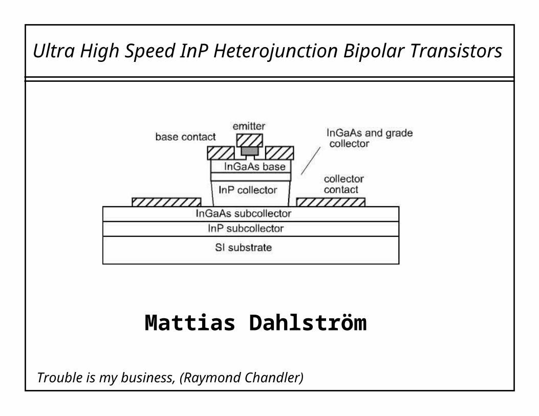
Ultra High Speed InP Heterojunction Bipolar Transistors
Mattias Dahlström
Trouble is my business, (Raymond Chandler)
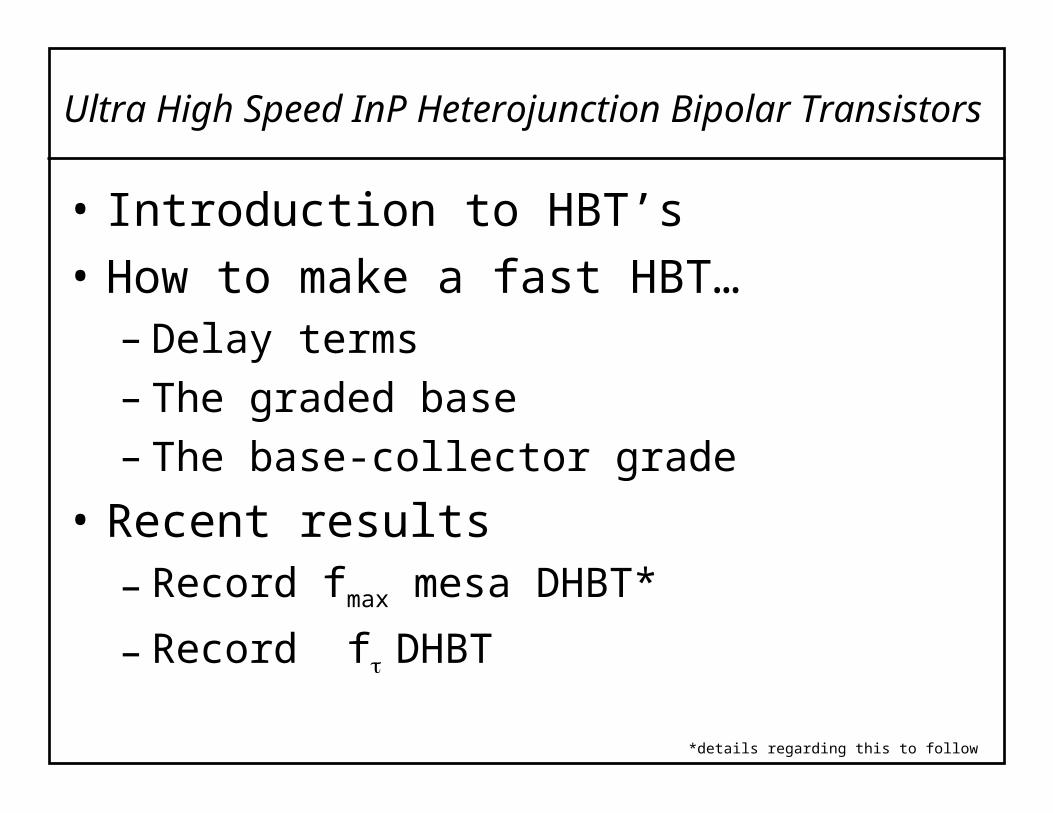
Ultra High Speed InP Heterojunction Bipolar Transistors
• Introduction to HBT’s
• How to make a fast HBT…– Delay terms– The graded base– The base-collector grade
• Recent results– Record fmax mesa DHBT*
– Record f DHBT
*details regarding this to follow

The transistor
0
5
10
15
20
25
30
0
1
2
3
4
5
6
7
0 0.5 1 1.5 2 2.5
J (A/um
2 )I C (
mA
)V
CE (V)
Ib in 200 A steps
Schematic of an HBT Typical common-emittercharacteristics
Small change in base current large change in collector current

InP lattice structure
Nearest neighbor: 2.5 ALattice constant:5.86 A
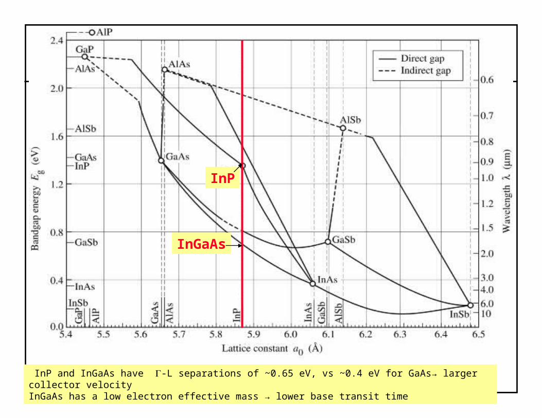
InP and InGaAs have -L separations of ~0.65 eV, vs ~0.4 eV for GaAs→ larger collector velocityInGaAs has a low electron effective mass → lower base transit time
InGaAs
InP

Objectives and approachObjectives:fast HBTs → mm-wave power, 160 Gb fiber opticsdesired: 440 GHz ft & fmax, 10 mA/m2, Ccb/Ic<0.5 ps/Vbetter manufacturability than transferred-substrate HBTsimproved performance over transferred-substrate HBTs
Approach:
narrow base mesa → moderately low Ccb
very low base contact resistance required, and good alignment → carbon base doping, good base contact process
high ft through high current density, thin layers
bandgap engineering: small device transit time with wide bandgap emitter and collector
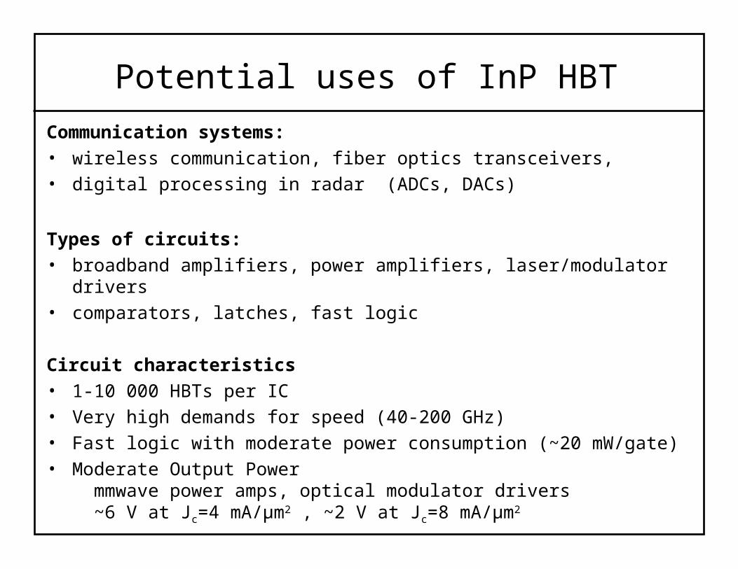
Potential uses of InP HBT
Communication systems:• wireless communication, fiber optics transceivers, • digital processing in radar (ADCs, DACs)
Types of circuits:• broadband amplifiers, power amplifiers, laser/modulator drivers• comparators, latches, fast logic
Circuit characteristics • 1-10 000 HBTs per IC• Very high demands for speed (40-200 GHz)• Fast logic with moderate power consumption (~20 mW/gate)• Moderate Output Power
mmwave power amps, optical modulator drivers ~6 V at Jc=4 mA/μm2 , ~2 V at Jc=8 mA/μm2
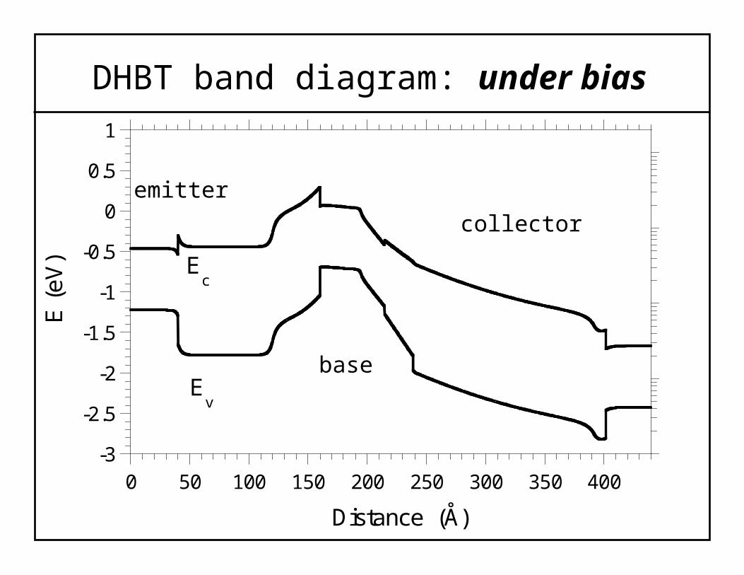
DHBT band diagram: under bias
-3
-2.5
-2
-1.5
-1
-0.5
0
0.5
1
0 50 100 150 200 250 300 350 400
E (
eV)
Distance (Å)
Ec
Ev
base
emitter
collector
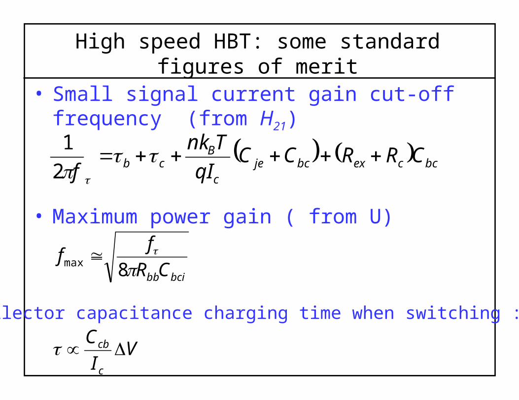
High speed HBT: some standard figures of merit
• Small signal current gain cut-off frequency (from H21)
• Maximum power gain ( from U)
bccexbcjec
Bcb CRRCC
qI
Tnk
f
2
1
bcibbCR
ff
8max
VI
C
c
cb
•Collector capacitance charging time when switching :
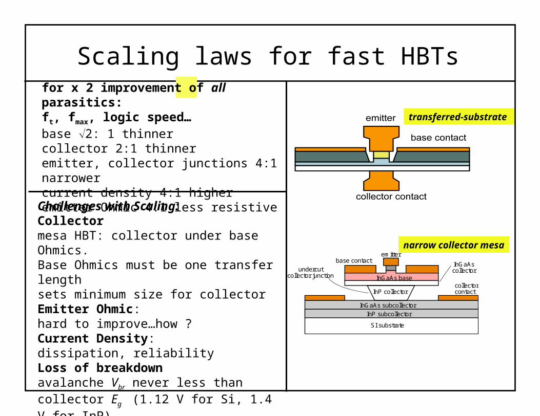
Scaling laws for fast HBTsfor x 2 improvement of all parasitics: ft, fmax, logic speed…base 2: 1 thinnercollector 2:1 thinneremitter, collector junctions 4:1 narrowercurrent density 4:1 higheremitter Ohmic 4:1 less resistive
Challenges with Scaling:Collector mesa HBT: collector under base Ohmics. Base Ohmics must be one transfer lengthsets minimum size for collector Emitter Ohmic: hard to improve…how ?Current Density: dissipation, reliabilityLoss of breakdownavalanche Vbr never less than collector Eg (1.12 V for Si, 1.4 V for InP) ….sufficient for logic, insufficient for power
emitterbase contact
collectorcontact
SI substrate
InGaAs subcollector
InP collector
InGaAscollector
InP subcollector
InGaAs base
undercutcollector junction
narrow collector mesa
transferred-substrate
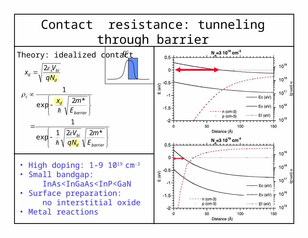
Contact resistance: tunneling through barrier
• High doping: 1-9 1019 cm-3
• Small bandgap: InAs<InGaAs<InP<GaN• Surface preparation: no interstitial oxide• Metal reactions
Theory: idealized contact
barrierd
bi
barrier
d
c
Em
qNV
Emx
*221exp
1
*2exp
1
d
bisd qN
Vx
2
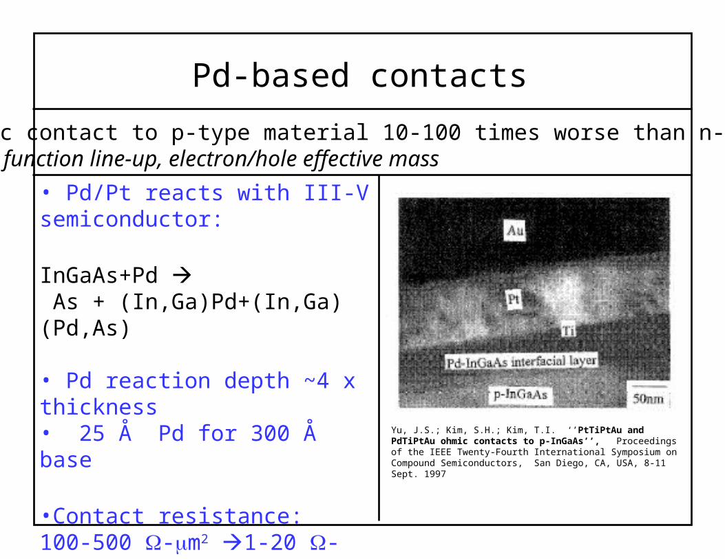
Pd-based contacts
• Pd/Pt reacts with III-V semiconductor:
InGaAs+Pd As + (In,Ga)Pd+(In,Ga)(Pd,As)
• Pd reaction depth ~4 x thickness• 25 Å Pd for 300 Å base
•Contact resistance: 100-500 -m2 1-20 -m2
from TLM and RF-extraction
Ohmic contact to p-type material 10-100 times worse than n-type.Work function line-up, electron/hole effective mass
Yu, J.S.; Kim, S.H.; Kim, T.I. ‘’PtTiPtAu and PdTiPtAu ohmic contacts to p-InGaAs’’, Proceedings of the IEEE Twenty-Fourth International Symposium on Compound Semiconductors, San Diego, CA, USA, 8-11 Sept. 1997

Emitter resistance
bccexbcjec
Bcb CRRCC
qI
Tnk
f
2
1
ee
ecex WL
R ,

Emitter resistance: grades removed
At degenerate doping levels grades are not necessary
-1.2
-0.8
-0.4
0
0.4
1012
1013
1014
1015
1016
1017
1018
1019
0 50 100 150 200 250 300 350 400
E (
eV)
n (cm-3
)
Distance (Å)
Ec
Ev
electrons
-1.6
-1.2
-0.8
-0.4
0
1015
1016
1017
1018
1019
0 50 100 150 200 250 300 350 400
E (
eV)
n (cm-3
)
Distance (Å)
Ec
Ev
electrons Contact resistance:50 m2 25 m2 15 m2
High doping 3 1019 cm-3
No InGaAs-InP grade necessary at very high doping
Thin undepleted n- emitter
Small emitter area increases Rex
InGaAscap layer InP
emitter
light doping
heavy doping

Base resistance
bcibbCR
ff
8max
Rbb is a critical parameter for fmax, and in npn HBT the base contact resistance dominates.Rbb is minimized through high base doping and improved base contact metallization, small undercut Wgap, and long emitter Le
eesspread
egapsgap
ecscontb
spreadgapcontbbb
LWR
LWR
LR
RRRR
12
2
2,
,
TLM measurement
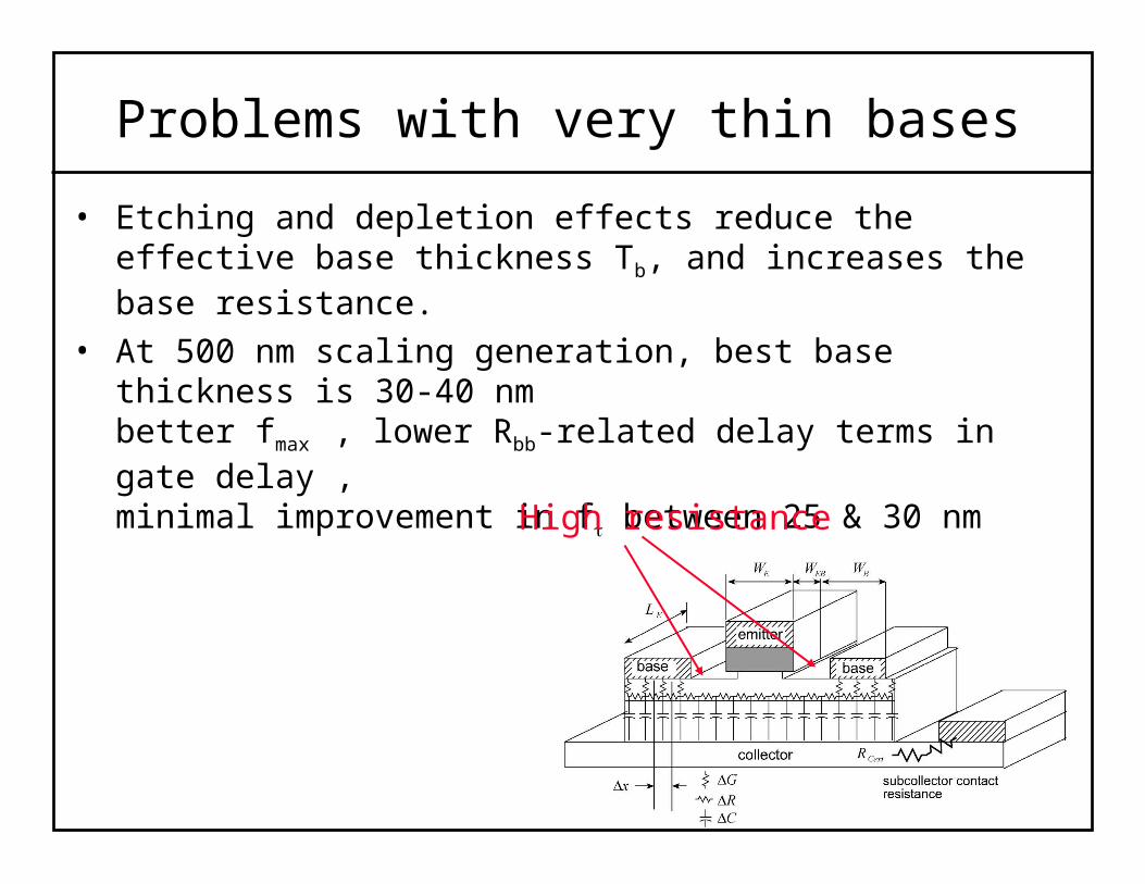
Problems with very thin bases
• Etching and depletion effects reduce the effective base thickness Tb, and increases the base resistance.
• At 500 nm scaling generation, best base thickness is 30-40 nmbetter fmax , lower Rbb-related delay terms in gate delay ,minimal improvement in f between 25 & 30 nm
High resistance

Increase of sheet resistance with thin base layers
A 51~
intrinsic,extrinsic, bb TTT-1
-0.5
0
0.5
1
1012
1013
1014
1015
1016
1017
1018
1019
1020
0 50 100 150 200 250 300
E (
eV) p (cm
-3 )
Distance (Å)
Ec
Ev
InGaAs base doped 6 1019 cm-3, surface pinned at 0.18 eV.
Surface depletion decreases base thickness 40 Å.
d
bisd qN
Vx
2 extrinsic,
intrinsic,intrinsic,extrinsic,
b
bbb R
RTT
Rb,extrinsic=800-1000 Ω/sqRb,intrinsic=600-750 Ω/sq
A 17~
intrinsic,extrinsic, bb TTT
Base protected by E/B grade(contacts diffused through 160 Å grade)
Surface depletionWet etching
Base surface exposed :
T~
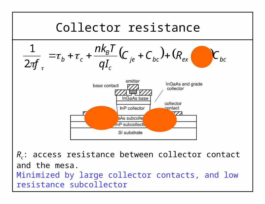
Collector resistance
bccexbcjec
Bcb CRRCC
qI
Tnk
f
2
1
Rc: access resistance between collector contact and the mesa. Minimized by large collector contacts, and low resistance subcollector
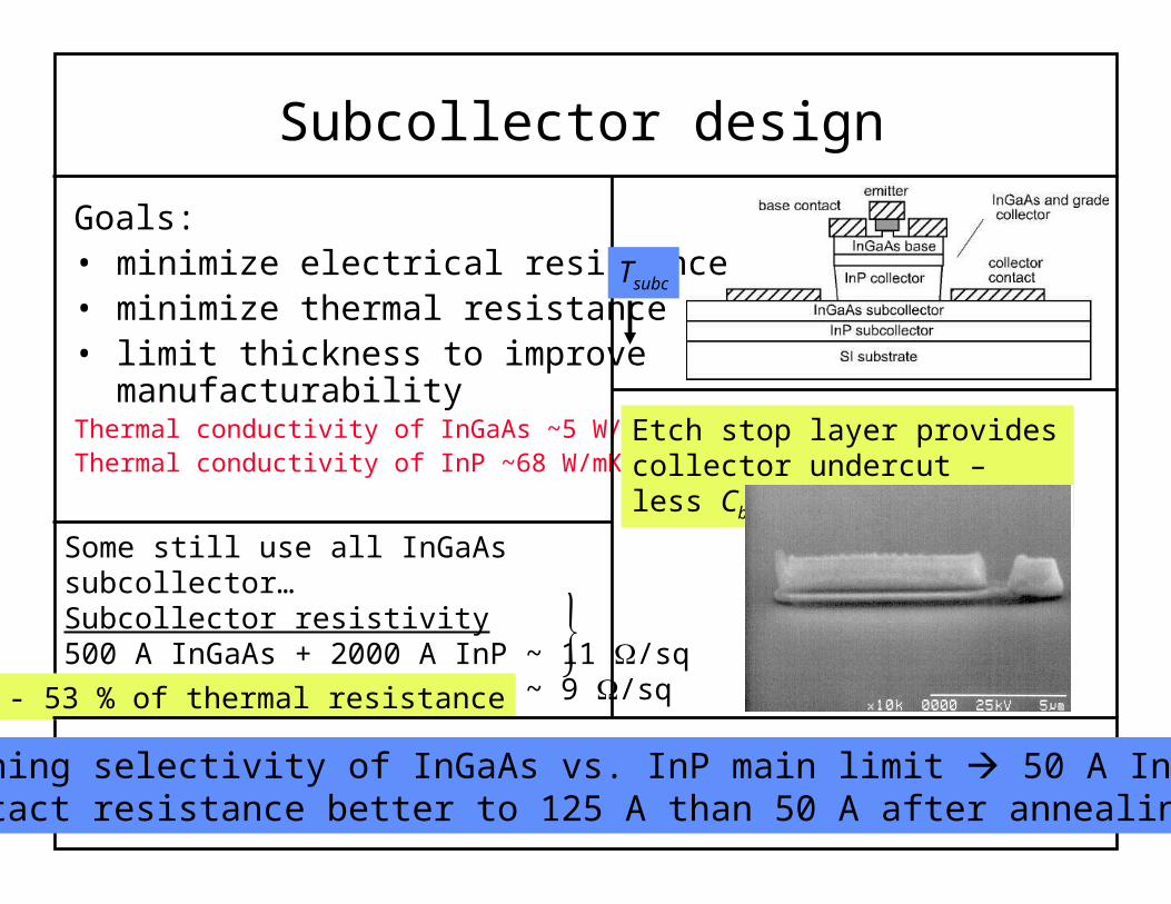
Subcollector design
Some still use all InGaAs subcollector…Subcollector resistivity500 A InGaAs + 2000 A InP ~ 11 /sq125 A InGaAs + 3000 A InP ~ 9 /sq
Etching selectivity of InGaAs vs. InP main limit 50 A InGaAsContact resistance better to 125 A than 50 A after annealing
Goals: • minimize electrical resistance • minimize thermal resistance• limit thickness to improve
manufacturabilityThermal conductivity of InGaAs ~5 W/mKThermal conductivity of InP ~68 W/mK
Tsubc
Etch stop layer provides collector undercut – less Cbc
- 53 % of thermal resistance

Base-emitter capacitance
bccexbcjec
Bcb CRRCC
qI
Tnk
f
2
1
Cje is the junction capacitance between the emitter and baseCje corresponds to ~100 Å depletion thickness
Minimized by shrinking the emitter area at fixed or at increasing current Ic
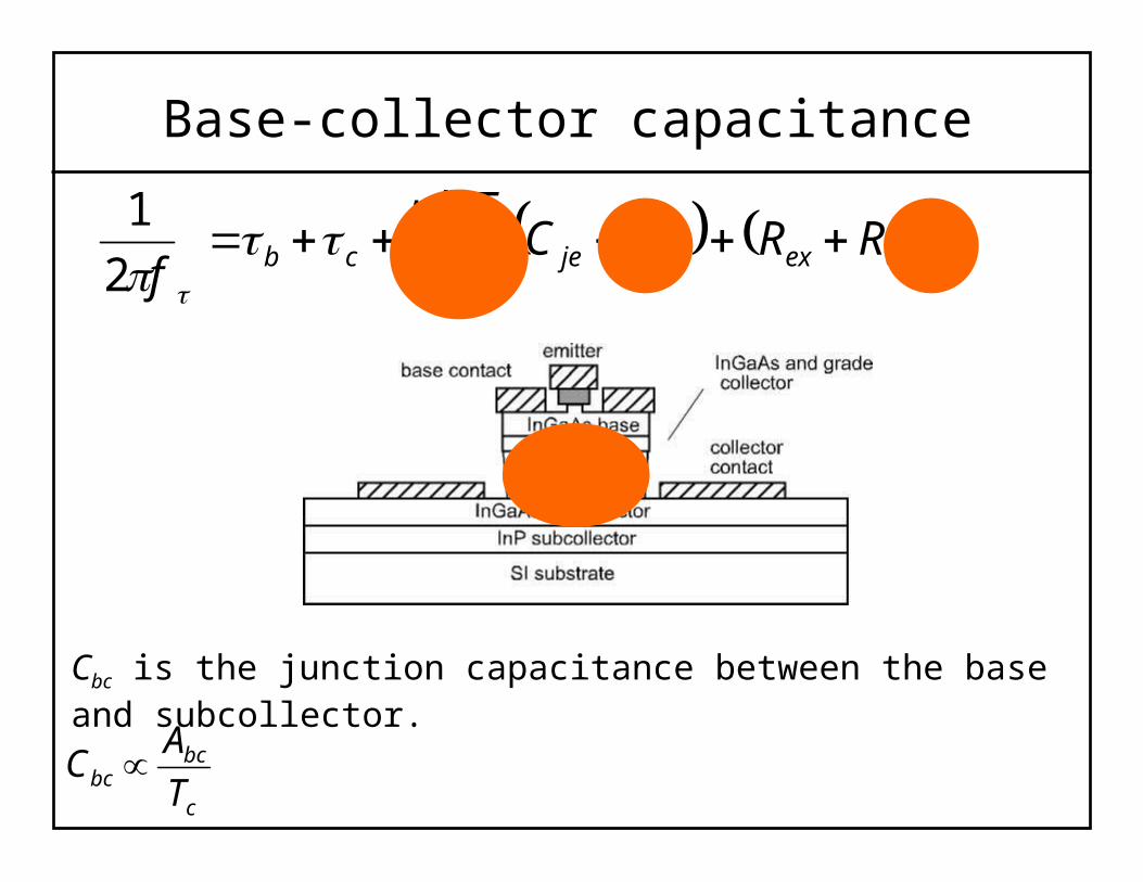
Base-collector capacitance
bccexbcjec
Bcb CRRCC
qI
Tnk
f
2
1
Cbc is the junction capacitance between the base and subcollector.
c
bcbc T
AC

Base-collector capacitance
c
bcbc T
AC
Tc = 3000 A 2150 A 1500 A
Abc must be kept small:• narrow emitter• narrow base contacts• undercut of base contacts
• implant or regrowth
Breakdown limits thickness
Thickness (A) Breakdown (V)
2150 7.5
1500 4-5
Collector thickness reduced due to speed requirements:
Ccb increases !
yinstabilit thermal
heating,by ndestructio
J highat decreases
ingby tunnell limited
collectors Very thin
/
collectors Thin
:collectorsThick
,
br
br
InPgapbr
cbr
V
V
qEV
TV

Theory of the base
If gain is limited by Auger recombination in the base:
22
,2
ba
baseeRB
TN
TAk
basen
bb D
T
,
2
2
is 100-250 fs)(calcb
is 10-50 • Decreasing increases . • High Na and Tb for low s decreases• Grade gives 30-50 % improvement
b
babasehs TNq ,
1
The base sheet resistance:
The base transit time:
ps is 400-900 /sq
Base Transit Time
dzdxznzD
zN
xN
xndx
J
Q bbb T
x iz
a
T
a
i
T
c
bb
)()(
)(
)(
)(2
0
2
0
)N - (N D )N-N D (
e D eN e N )N e D e N e
a1i11a1i11
) WN WD - D - W(-N1
)(-D a1
)(-Di1i1
)D - W(-D1
)D - W(-Da1
)D - W(-D
int,
ba1b12bi1222b12b12b1
b
bT
bi
i
a
baexit Tn
xn
xN
TN
02
2
)(
)(
)(
)(
)N-)(N(Tnv
)e- (e )(TN
a1i1b2is
)N-(N)N-TN-NT(Nba
a2i2a2ba1i2bi1
exit
Fitting of relevant parameters of the form )()( BAzexf
With doping as
)( 21 aa NzNa eN
Intrinsic carrier concentration )(2 21 ii NzN
i en
Diffusivity
)( 21 DzDeD
Kroemer’s double integral:Drift-Diffusion equation for base current:
Exit term
Solution used for evaluation of the base transit time:
2bT
exitb vT Ballistic injection: bT
qdx
dqJ n
nn
0pJ

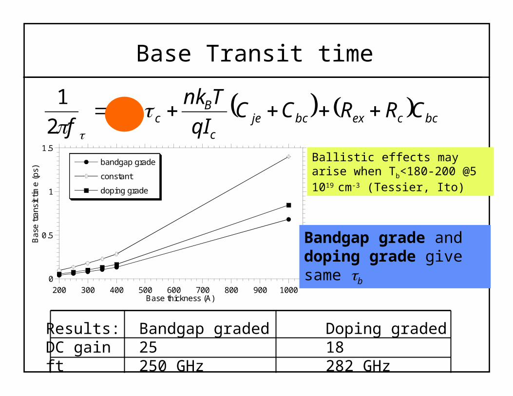
Base grading
Graded bandgap Graded doping
Doping 8 5 1019 cm-3Change in In:Ga ratioInAs: Eg=0.36 eVGaAs: Eg=1.43 eV

Base grading: induced electric field
Induced electric field accelerates electrons towardscollector – decreases base transit time and increases gain
Limits: strain Limits: Bandgap narrowing, needs degenerate doping

The effect of degenerate doping
Evidence: Observed Vbe increase Von ~ φbi , increases with Ev
Nb=4 1019cm30.75 VNb=8 1019cm30.83 Vfor graded base-emitter
Strong variation in Fermi-level with doping at high doping levels

Base bandgap narrowing
Model after V. Pavlanovski
Bandgap grade
Doping grade
BGN provides an electric field opposing the doping-induced field.
~1:5 in magnitude
0
0.5
1
1.5
200 300 400 500 600 700 800 900 1000
Base transit time
bandgap grade
constant
doping grade
Ba
se tr
ans
it tim
e (
ps)
Base thickness (A)
Base Transit time
Ballistic effects may arise when Tb<180-200 @5 1019 cm-3 (Tessier, Ito)
Results: Bandgap graded Doping gradedDC gain 25 18ft 250 GHz 282 GHz
bccexbcjec
Bcb CRRCC
qI
Tnk
f
2
1
Bandgap grade and doping grade give same b
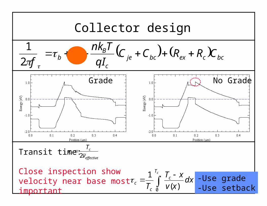
Collector design
Transit time:
Close inspection show velocity near base most important
effective
cc v
T
2
Grade No Grade
dxxv
xT
Tc
T
cc
c
)(
1
0
-Use grade
-Use setback
bccexbcjec
Bcb CRRCC
qI
Tnk
f
2
1

-2
-1.5
-1
-0.5
0
0.5
1
0 50 100 150 200
E (
eV)
Distance (Å)
Ev
Ec
-2
-1.5
-1
-0.5
0
0.5
1
1.5
0 50 100 150 200
E (
eV)
Distance (Å)
Ev
Ec
Base-collector grade
Early grade designs:• Too coarse• No setback layer
Recent grade designs:• 15 A period• 200 A setback layer
Gain: 7f: 128 GHz (Tc=3000 A)Jkirk: 1.3 mA/μm2
Gain: 27f: 282 GHz (Tc=2150 A)Jkirk: 4 mA/μm2

InAlAs/InGaAs super lattice
• Why super lattice?– MBE is more suited for super lattice than
quaternaries.– InP/InGaAs gives poor quality material due to
phosphorous-arsenic intermixing
• MOCVD growth → InGaAsP grade
• GaAsSb base needs no grade

• Quantum well trapping• Electron/hole in the InGaAs well• 500 meV InAlAs potential barrier
A rough approximation: the infinite potential well.
....3,2,1....2 2
222
nma
nEn
If En> 500 meV (InGaAs/InAlAs potential) no electron confinement ~31 A is the maximum allowed InGaAs width by this model
Quantum mechanical trapping in grade

The delta-doping
grade
cr
Tq
ETN
2
H. Kroemer : a conduction band difference can be offset with a grade and a delta-doping
With this choice the conduction band will be smooth
No delta-doping Delta-dopingVbc=0.3 V Vbc=0.3 V

The setback layer
• An InGaAs layer beneath the base – Margin for Base dopant diffusion– Increases Electron speed at SL
SetbackVbc=0.3 V
No setbackVbc=0.3 V

Collector design: doping
2max,
min,
)(2
dopingcollector allowable maximum thespecifies This
ECL)in Volts 0.0 (e.g. specified minimum someat
)(low collector depletedfully a want illdesigner wCircuit
CqT
VN
V
C
cbd
cb
cb
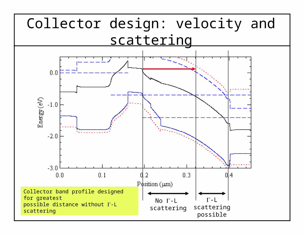
Collector design: velocity and scattering
No -L scattering
-L scatteringpossible
Collector band profile designed for greatestpossible distance without -L scattering

Collector under current (simulation)
-2
-1.5
-1
-0.5
0
0.5
0 100 200 300 400
J=0mAJ=1mAJ=2mAJ=3mAJ=4mAJ=5mAJ=6mAJ=7mAJ=8mA
E (
eV
)
Position (A)
Nc reduced by Jc/q/vsat
Current blocking
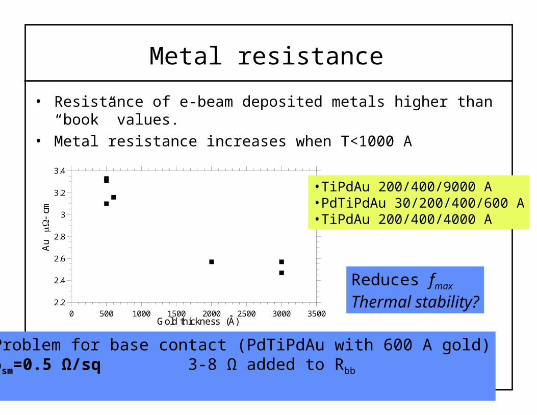
Metal resistance
• Resistance of e-beam deposited metals higher than “book” values.
• Metal resistance increases when T<1000 A
2.2
2.4
2.6
2.8
3
3.2
3.4
0 500 1000 1500 2000 2500 3000 3500
Au
cm
Gold thickness (Å)
Problem for base contact (PdTiPdAu with 600 A gold)sm=0.5 Ω/sq 3-8 Ω added to Rbb
•TiPdAu 200/400/9000 A•PdTiPdAu 30/200/400/600 A•TiPdAu 200/400/4000 A
Reduces fmax
Thermal stability?

Results
• 2150 A collector high fmax, high Vbr,CEO
IPRM 2002, Electron Device Letters, Jul. 2003; M. Dahlström et al, ''Ultra-Wideband DHBTs using a Graded Carbon-Doped
InGaAs Base''
• 1500 A collector high f, high fmax , high Jc
Submitted to DRC 2003; M. Dahlstrom, Z. Griffith et al.,“InGaAs/InP DHBT’s with ft and fmax over 370 GHz using Graded
Carbon-Doped Base”
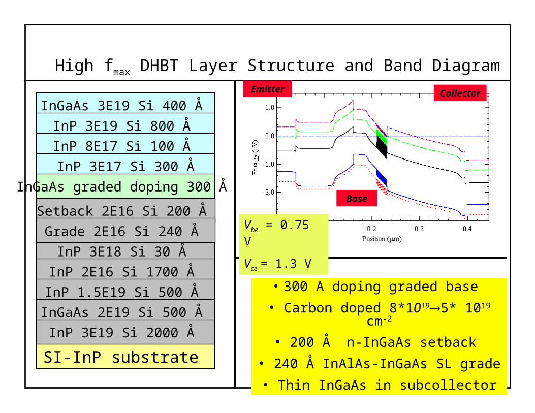
InGaAs 3E19 Si 400 Å
InP 3E19 Si 800 Å
InP 8E17 Si 100 Å
InP 3E17 Si 300 Å
InGaAs graded doping 300 Å
Setback 2E16 Si 200 Å
InP 3E18 Si 30 Å
InP 2E16 Si 1700 Å
SI-InP substrate
Grade 2E16 Si 240 Å
InP 1.5E19 Si 500 Å
InGaAs 2E19 Si 500 Å
InP 3E19 Si 2000 Å
• 300 A doping graded base
• Carbon doped 8*10195* 1019 cm-2
• 200 Å n-InGaAs setback
• 240 Å InAlAs-InGaAs SL grade
• Thin InGaAs in subcollector
High fmax DHBT Layer Structure and Band Diagram
Vbe = 0.75 V
Vce = 1.3 V
Emitter Collector
Base

InGaAs 3E19 Si 400 Å
InP 3E19 Si 800 Å
InP 8E17 Si 100 Å
InP 5E17 Si 400 Å
InGaAs graded doping 300 Å
Setback 3E16 Si 200 Å
InP 3E18 Si 30 Å
InP 3E16 Si 1030 Å
SI-InP substrate
Grade 3E16 Si 240 Å
InP 1.5E19 Si 500 Å
InGaAs 2E19 Si 125 Å
InP 3E19 Si 3000 Å
• Thinner InP collector
•Collector doping increased to 3 1016 cm-3
• Thinner InGaAs in subcollector
•Thicker InP subcollector
High f DHBT Layer Structure and Band Diagram
Vbe = 0.75 V
Vce = 1.3 V
Emitter Collector
Base

Results: DC
0
2
4
6
8
10
0 0.5 1 1.5 2 2.5
J c (m
A/
m2 )
Vce
(V)
Ajbe
=0.6 x 7 m2
Vcb
= 0 V
Ib step
= 0.4 mA
0
1
2
3
4
5
0 0.5 1 1.5 2 2.5 3
I C (
mA
)
VCE
(V)
emitter junction area: 0.44 m x 7.4 mIB step = 50 uA
0
0.5
1
1.5
2
2.5
3
0 1 2 3 4 5 6 7 8
High fmax DHBT High f DHBT
Gain: 23-28nb/nc: 1.05/1.44Vbr,CEO: 7 V
Gain: 8-10nb/nc: 1.04/1.55Vbr,CEO:4 V
No evidence of current blocking or trapping

Results: RF
0
5
10
15
20
25
30
1010 1011 1012
Gai
n (
dB)
Frequency (Hz)
f=282 GHz
fmax
=400 GHzU
H21
Ajbe
= 0.54 x 7.6 um2
Ic = 15 mA
J = 3.6 mA/um2 , Vce
= 1.7 V
High fmax DHBT High f DHBT
0
5
10
15
20
25
30
1010 1011 1012
Ga
ins
(dB
)
Frequency (Hz)
ft= 370 GHz
fmax
=375 GHzU
H21
MAG/MSG
Ajbe
= 0.6 x 7 um2
Ic = 30 mA
J = 7.2 mA/um2 , Vce
= 1.3V
• Highest fmax for mesa HBT • Highest f for mesa DHBT• Highest (f, fmax) for any HBT• High current density

Results: Base width dependence
260
270
280
290
300
310
320
330
f t (G
Hz)
Wb=0.3 m W
b=0.5 m W
b=1.0 m
Je=5.9 mA/m
2
Je=7.2 mA/m
2
260
270
280
290
300
310
320
f max
(G
Hz)
Wb=0.3 m W
b=0.5 m W
b=1.0 m
Je=5.9 mA/m
2
Je=7.2 mA/m
2
Emitter junction 0.6 x 7 m, Vce=1.3 VTb=300 A. Tc=1500 A
bcibbCR
ff
8max
bccexbcjec
Bcb CRRCC
qI
Tk
f
2
1
f maxf
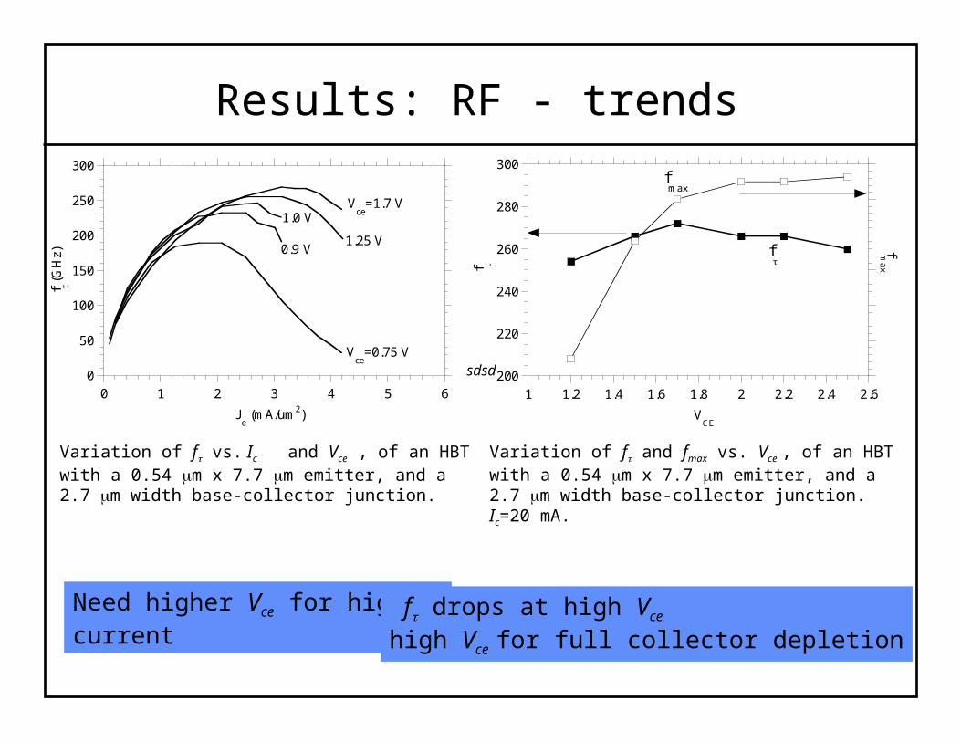
Results: RF - trends
0
50
100
150
200
250
300
0 1 2 3 4 5 6
f t (G
Hz)
Je (mA/um2)
0.9 V
1.0 VV
ce=1.7 V
Vce
=0.75 V
1.25 V
200
220
240
260
280
300
1 1.2 1.4 1.6 1.8 2 2.2 2.4 2.6
f t
fmax
VCE
f
fmax
Variation of f vs. Ic and Vce , of an HBT with a 0.54 m x 7.7 m emitter, and a 2.7 m width base-collector junction.
Variation of f and fmax vs. Vce , of an HBT with a 0.54 m x 7.7 m emitter, and a 2.7 m width base-collector junction. Ic=20 mA.
sdsd
Need higher Vce for high current f drops at high Vce
high Vce for full collector depletion

Results: evolution
100
150
200
250
300
350
400
DHBT3 DHBT6 DHBT9 DHBT18
f t (G
Hz)
f fmax
100
150
200
250
300
350
400
450
DHBT3 DHBT6 DHBT9 DHBT18
f max
(G
Hz)Final grade
Old grade
New grade
0
1 105
2 105
3 105
4 105
5 105
6 105
7 105
8 105
DHBT3 DHBT6 DHBT9 DHBT18
J opt (
mA
/um
2)
DHBT 19B
Strong improvement in f and Jopt
Jopt
f and fmax > 200 GHz at Jc >10 mA/m2
Tc =1500 A

Capacitance vs. current
16
16.5
17
17.5
18
18.5
0 1 2 3 4 5 6 7 8
Ccb
(fF
)
Je (mA/um2)
Vce
=1.5 V
Vce
=1.3 V
Emitter junction 0.5x7.6 umTc= 1500 A, Nc=3 1016 cm-3
DHBT 20Graded emitter base junction
DHBT 17Abrupt emitter base junction
Emitter junction 0.54x7.6 um and 0.34x7.6 um. Tc= 2150 A, Nc=2 1016 cm-3
2max
1
ckirk T
JJ
10
11
12
13
14
15
16
0 1 2 3 4 5 6
Ccb
(fF
)
Je (mA/um2)
Vce
=1.5 V
Vce
=1.7 V
Vce
=1.7 V
Jmax~3 mA/m2 Jmax~6.5 mA/m2
48 % Jmax~3.2 mA/m2 for Tc=2150 A

Area dependence on capacitance reduction
0
5
10
15
20
25
30
0.1 0.15 0.2 0.25 0.3 0.35 0.4
CC
B r
ed
uct
ion
(%
)
Emitter to basemesa ratio
Vce
=1.5-1.7 V
DHBT 17
DHBT 17
DHBT 18
DHBT 19
DHBT 20DHBT 20
DHBT 19
DHBT 20
DHBT 19
DHBT 20DHBT 20
We
BB
C
E
Wbc
bc
e
W
Wratio
Ccb from Y-parametersat 5 GHz
Vce=1.3 V
Vce=1.5 V
Extrapolating with linear fit gives 55 % for r=1
Ccb is reduced where the current flows reduce extrinsic base

Max current density vs. emitter size
The current at which Ccb increases (Jmax) as a function of emitter width for two different HBT
3
4
5
6
7
8
0.2 0.4 0.6 0.8 1 1.2 1.4
Emitter width (m)
Vce
=1.5 V
Tc=1500 A
J C
(m
A/u
m2)
Vce
=1.7 V
Tc=2150 A
• Narrow emitters have higher critical current density• Not necessarily higher ft (due to Rex) - Current spreading
200
220
240
260
280
300
2 2.5 3 3.5 4 4.5 5 5.5 6
f t (G
Hz)
Je (mA/um2)
We=0.5 m
We=0.7 m
We=0.6 m

Calculation of current spreading
cc
r v
xJqN
dx
d )(1E
e
c
de
eee
LT
xLW
LWJxJ
2
)(
1
22
21ln2
21ln
2
d
e
dd
e
de
d
e LW
LL
W
LW
L
W
VV
TqNvJ bcbi
c
rcckirk 2
2
• Poisson’s equation with depth dependant current J(x)
• Solving double integral provides Kirk threshold correction term
• J now has emitter width dependencecced DL ,
ee WL
0)0( xE
at Jkirk
Lateral diffusion
One-dimension
Kirk condition

Summary of delay terms
Tau_ec 503.65 fs
RexCcb 31.4 fs 6.1 %RexClay 11.27 fs 2.2 %tau_f 385.62 fs 75.3 %
kT/qI times Cje 48 fs 9.4 %kT/qI times Ccb 26 fs 5.1 %kT/qI times Clayout 9 fs 1.8 %
SUM 512 fs 100.0 %
ft_corr 311 GHz Rex-related 8.3 %ft_meas 316 GHz

Emitter heat sinking
Emitter interconnect metal 2 μm to 7 μm
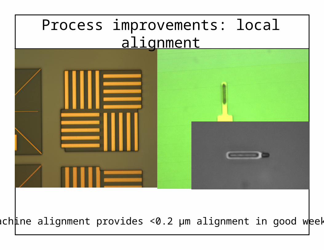
Process improvements: local alignment
Machine alignment provides <0.2 μm alignment in good weeks

Process improvements: lift-off
• Improved hardening of top resist surface• 0.4 x 8 μm emitters, ~1 μm thick

What to do in the future: short term
• Have new material with InAs rich emitter cap less Rex increased f
• Doping grade and combined grade less b increased f ?
• Small scale circuits by Z. Griffith and others• Write paper on Kirk effect / collector current spreading
Hålls me slåttern

What to do in the future: long term
• Need a more SiGe like processing technology– Lift-off– Isolation – Emitter regrowth
• Work on HBT design– Emitter design– Base grade
• See circuits come out …
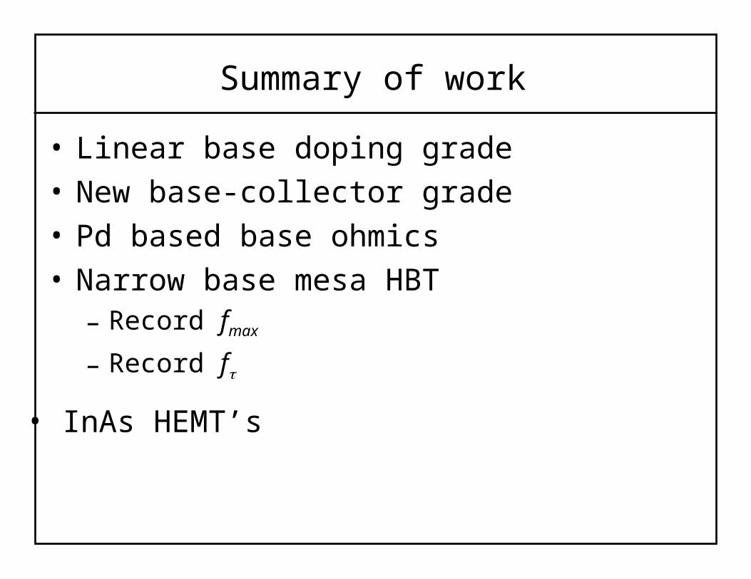
Summary of work
• Linear base doping grade
• New base-collector grade
• Pd based base ohmics
• Narrow base mesa HBT– Record fmax
– Record f
• InAs HEMT’s
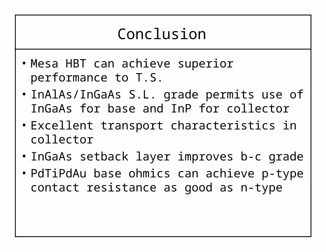
Conclusion
• Mesa HBT can achieve superior performance to T.S.
• InAlAs/InGaAs S.L. grade permits use of InGaAs for base and InP for collector
• Excellent transport characteristics in collector
• InGaAs setback layer improves b-c grade
• PdTiPdAu base ohmics can achieve p-type contact resistance as good as n-type

in case of questions

Results: base-collector capacitance
0
10
20
30
40
50
60
70
0 1 2 3 4 5
Ccb
(fF
)
Je (mA/um2)
0.75 V
Vce
=1.7 V
1.1 V1.25 V
1.0 V
0.9 V
Full depletion
Variation of Ccb vs. Ic and Vce. Note that
Vbe=0.85-0.90 volts over the same bias range.

Hole mobility extraction
• With measured base sheet resistance and doping level the base hole mobility can be estimated
30
40
50
60
70
80
90
CBe
SHBT DHBT9 MHBT1 DHBT18 DHBT219 DHBT220
uh (
cm2 /
Vs)
30
40
50
60
70
80
90
2 1019 6 1019 1 1020 1.4 1020
Ba
se h
ole
mob
ility
(cm
2 / V
s)
Base doping cm-3
bbhs TNq
1
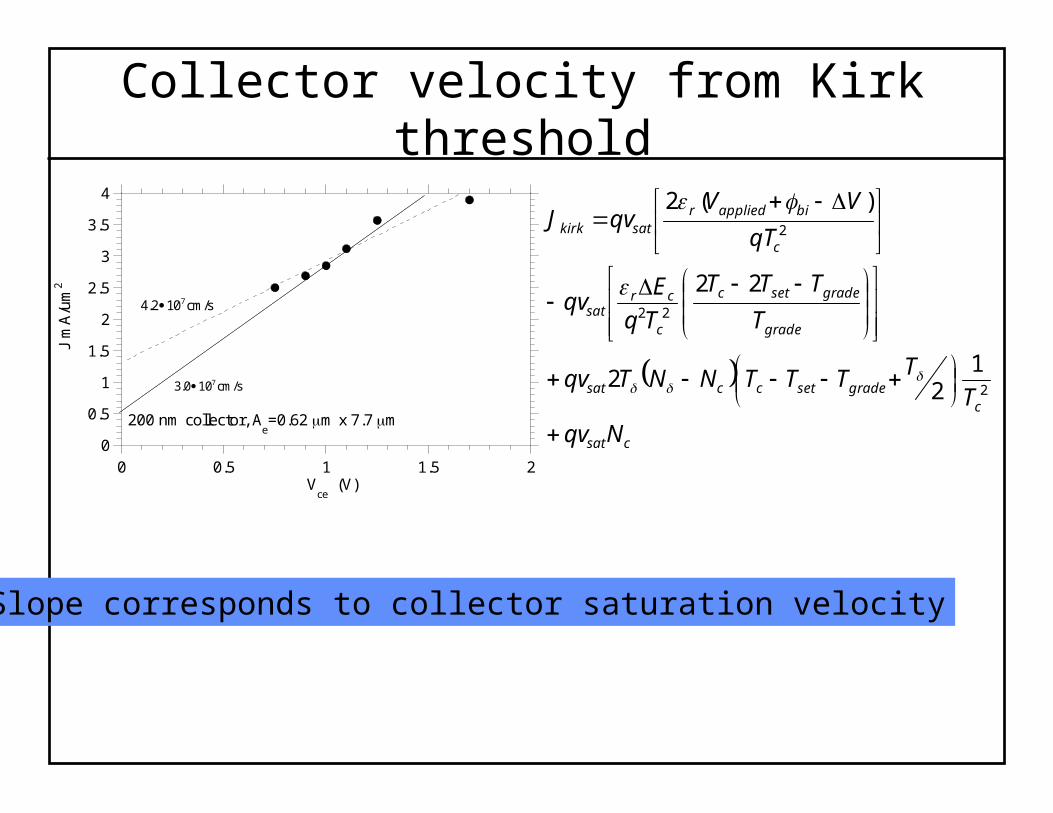
Collector velocity from Kirk threshold
0
0.5
1
1.5
2
2.5
3
3.5
4
0 0.5 1 1.5 2
J m
A/u
m2
Vce
(V)
200 nm collector, Ae=0.62 m x 7.7 m
cm/s102.4 7
cm/s100.3 7
csat
cgradesetccsat
grade
gradesetc
c
crsat
c
biappliedrsatkirk
Nqv
TTTTTNNTqv
T
TTT
Tq
Eqv
qT
VVqvJ
2
22
2
122
22
)(2
Slope corresponds to collector saturation velocity

Collector velocity from bc
0
100
200
300
400
500
600
0 1000 2000 3000
t c (fs
)
Tc (A)
sat
cc v
T
2
slopedTd
Tv
c
cc
csat
1
2
11
2
1
2
m/s1005.3
m/s1046.45
5
satv
m/s1005.3 5satv

InP-InGaAs and InP-GaAsSb
Base-collector grades necessary
Grades not necessary
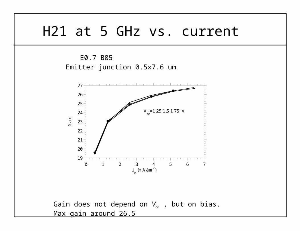
H21 at 5 GHz vs. current
19
20
21
22
23
24
25
26
27
0 1 2 3 4 5 6 7
Ga
in
Je (mA/um2)
Vce
=1.25 1.5 1.75 V
Emitter junction 0.5x7.6 umE0.7 B05
Gain does not depend on Vce , but on bias.Max gain around 26.5
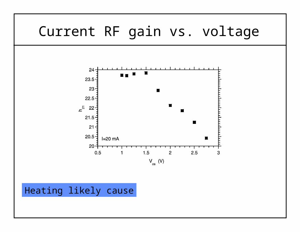
Current RF gain vs. voltage
Heating likely cause

Results: Gummel
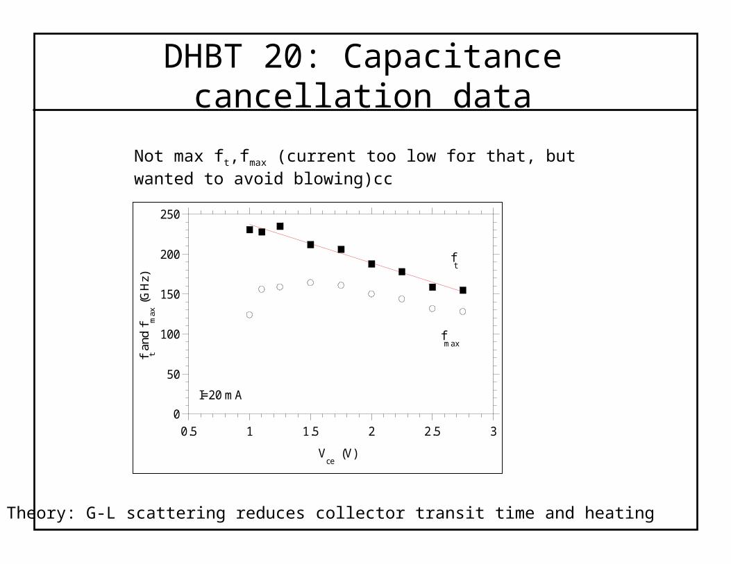
DHBT 20: Capacitance cancellation data
0
50
100
150
200
250
0.5 1 1.5 2 2.5 3
f t and
fm
ax (
GH
z)
Vce
(V)
I=20 mA
ft
fmax
Not max ft,fmax (current too low for that, but wanted to avoid blowing)cc
Theory: G-L scattering reduces collector transit time and heating

Capacitance cancellation
Previous slide CE
ec
CB
c
VV
f2
1ec
CB
cc
c
Ere,cb dV
dI
T
AC
0
2 10-13
4 10-13
6 10-13
8 10-13
1 10-12
1.2 10-12
0.5 1 1.5 2 2.5 3
t ec
Vce
(V)
I=20 mA
4/I fF/A
4 fF reduction from ft vs. Vce relation, very close to measured
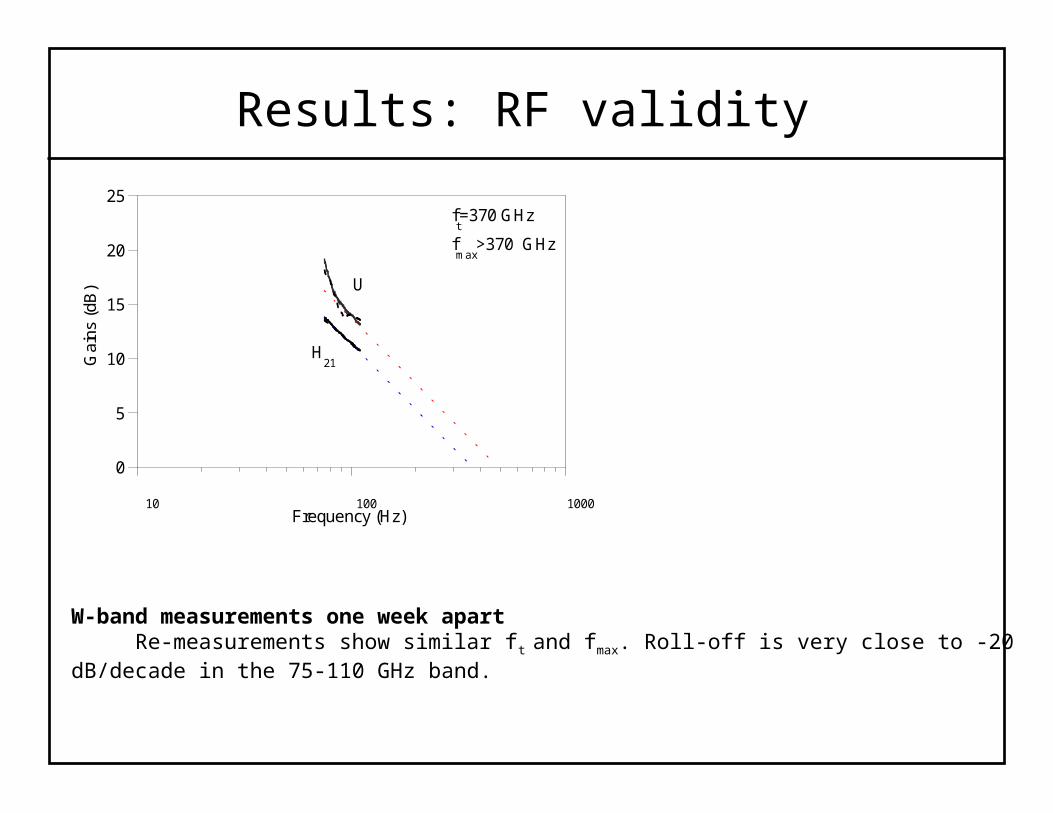
Results: RF validity
0
5
10
15
20
25
10 100 1000
Gai
ns (
dB)
Frequency (Hz)
ft=370 GHz
fmax
>370 GHz
U
H21
W-band measurements one week apart Re-measurements show similar ft and fmax. Roll-off is very close to -20 dB/decade in the 75-110 GHz band.

Resistance vs. doping
InGaAs and InP n-type doping : 1-3 1019 cm-3
InGaAs p-type doping 1.2 1020 cm-3: no p-InP with C doping
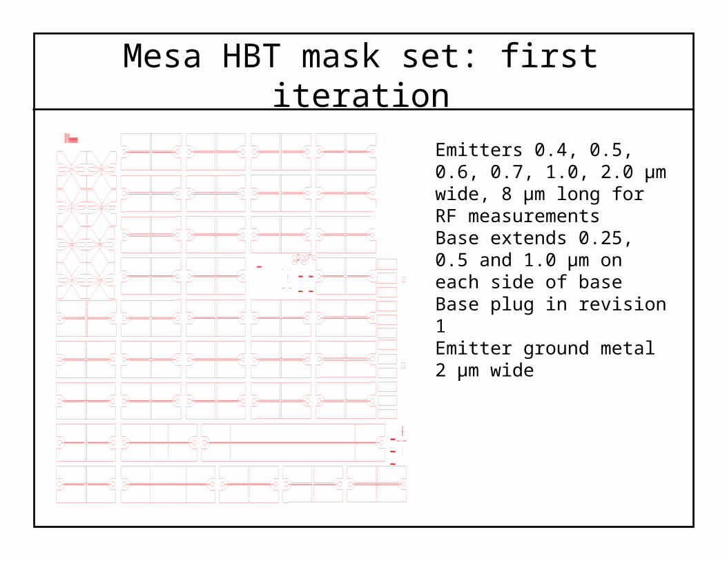
Mesa HBT mask set: first iteration
Emitters 0.4, 0.5, 0.6, 0.7, 1.0, 2.0 μm wide, 8 μm long for RF measurementsBase extends 0.25, 0.5 and 1.0 μm on each side of baseBase plug in revision 1Emitter ground metal 2 μm wide

Mesa HBT mask set: second iteration
Emitters 0.4, 0.5, 0.6, 0.7, 1.0, 2.0 μm wide, 8 μm long for RF measurementsBase extends 0.35, 0.5 and 1.0 μm on each side of baseBase plug now on smaller tennis-racquet handleEmitter ground metal extended to 7 μm width

RF measurements: CPW structure
230 m 230 m
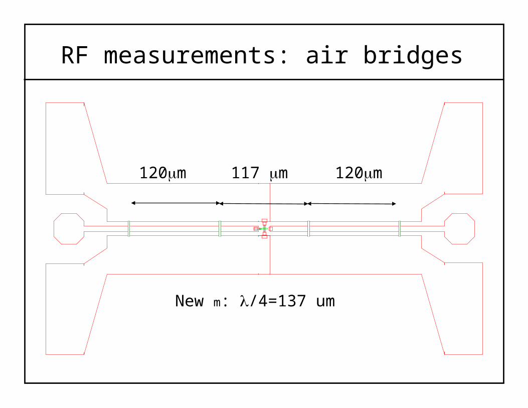
RF measurements: air bridges
120m
New m: /4=137 um
117 m 120m

RF measurements: calibration
• LRL calibration using on wafer Open, Zero-length through line, and delay line
• OLTS used to check U in DC-50 GHz band
• Probe pads separated by 460 m to reduce p-p coupling
• RF environment not ideal, need: thinning, air bridges, vias for parasitic mode suppression
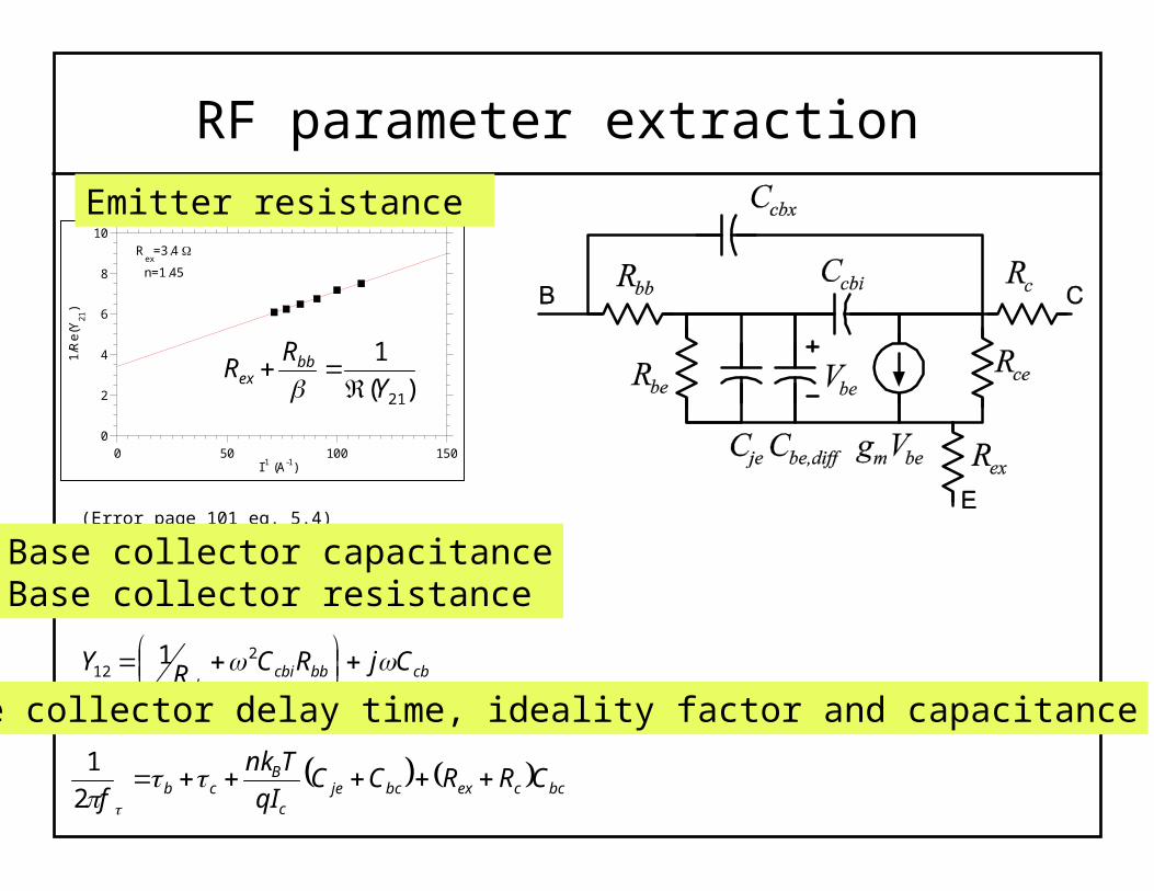
RF parameter extraction
0
2
4
6
8
10
0 50 100 150
1/R
e(Y
21)
I-1 (A-1)
Rex
=3.4
n=1.45
)(
1
21Y
RR bb
ex
Emitter resistance
(Error page 101 eq. 5.4)
cbbbcbicb
CjRCRY
2
121
Base collector capacitanceBase collector resistance
Base collector delay time, ideality factor and capacitance
bccexbcjec
Bcb CRRCC
qI
Tnk
f
2
1

I
VC
.
• Switching speed limited by output capacitance
How do we get speed improvement
Design Specifications set ΔV and RL sets I
Reduce C by decreasing AC
Increase in J since I fixed J limited by Kirk Effect Increase in J increase dissipated power density
Formula simplisticinsight

Can we measure Rth (Method of Lui et al )
0.50 0.520.48 0.54
0.002
0.004
0.006
0.008
0.000
0.010
VBE
IC.i
VBE
I_DCSRC2Idc=IB
L8E7B21X1
I_ProbeIC V_DC
SRC1Vdc=VCE
Ramp IB for different VCE
Measure VBE and IC
CCE
BET IV
VR
Depends on current density
2 3 4 5 6
x 10-3
1000
2000
3000
4000
5000
PAve
RT
Large uncertainty in values. Fitting regression curves helps to reduce error

Validation of Model
0
5
10
15
20
25
30
35
40
-0.2 0 0.2 0.4 0.6 0.8 1 1.2
centerEdge
Tem
per
atu
re R
ise
(K)
Distance from substrate (m)
SC ES C B E E Metal
Caused by Low K
of InGaAs
Max T in Collector
Ave Tj (Base-Emitter) =26.20°CMeasured Tj=26°CGood agreement.
Advice Limit InGaAs Increase size of emitter arm

Ultra High Speed InP Heterojunction Bipolar Transistors
Why this title?
• Some recent conference results show transistor f of 130 GHz…
• InP is a brittle semiconductor with a metallic luster. We mix it with GaAs and AlAs. Use Si and C as dopants
• Heterojunction: contains junctions of different materials

DHBT carrier profile
1015
1016
1017
1018
1019
1020
0 50 100 150 200 250 300 350 400-3
-2.5
-2
-1.5
-1
-0.5
0
0.5
1
N (cm
-3)
Distance (Å)
Base Collector
electrons
Emitter Subcollector
holes
quick comment that this is unbiased....under bias both DR will fill with E