Ultra-Configurable Multiple-Function Gate With 3-State Output
24
See mechanical drawings for dimensions. DCT PACKAGE (TOP VIEW) DCU PACKAGE (TOP VIEW) YZP PACKAGE (BOTTOM VIEW) 1 V CC 8 OE 2 7 A Y 3 6 B D 4 5 GND C 3 6 D B 8 1 V CC OE 5 GND 4 C 2 7 Y A GND 5 4 C 3 6 D B 2 7 Y A 8 V CC 1 OE SN74LVC1G99 www.ti.com SCES609G – SEPTEMBER 2004 – REVISED NOVEMBER 2013 Ultra-Configurable Multiple-Function Gate With 3-State Output Check for Samples: SN74LVC1G99 1FEATURES DESCRIPTION The SN74LVC1G99 device is operational from 1.65 V 2• Available in Texas Instruments to 5.5 V. NanoFree™ Package The SN74LVC1G99 device features configurable • Supports 5-V V CC Operation multiple functions with a 3-state output. The output is • Inputs Accept Voltages to 5.5 V disabled when the output-enable (OE) input is high. • Supports Down Translation to V CC When OE is low, the output state is determined by 16 patterns of 4-bit input. The user can choose logic • Max t pd of 6.7 ns at 3.3 V functions, such as MUX, AND, OR, NAND, NOR, • Low Power Consumption, 10-μA Max I CC XOR, XNOR, inverter, and buffer. All inputs can be • ±24-mA Output Drive at 3.3 V connected to V CC or GND. • Offers Nine Different Logic Functions in a This device functions as an independent inverter, but Single Package because of Schmitt action, it has different input • I off Supports Live Insertion, Partial-Power- threshold levels for positive-going (V T+ ) and negative- Down Mode, and Back-Drive Protection going (V T– ) signals. • Input Hysteresis Allows for Slow Input To ensure the high-impedance state during power up Transition Time and Better Noise Immunity at or power down, OE should be tied to V CC through a Input pullup resistor; the minimum value of the resistor is determined by the current-sinking capability of the • Latch-Up Performance Exceeds 100 mA Per driver. JESD 78, Class II This device is fully specified for partial-power-down • ESD Protection Exceeds JESD 22 applications using I off . The I off circuitry disables the – 2000-V Human-Body Model (A114-A) outputs, preventing damaging current backflow – 200-V Machine Model (A115-A) through the device when it is powered down. – 1000-V Charged-Device Model (C101) NanoFree™ package technologies are a major breakthrough in IC packaging concepts, using the die as the package. 1 Please be aware that an important notice concerning availability, standard warranty, and use in critical applications of Texas Instruments semiconductor products and disclaimers thereto appears at the end of this data sheet. 2NanoFree is a trademark of Texas Instruments. PRODUCTION DATA information is current as of publication date. Copyright © 2004–2013, Texas Instruments Incorporated Products conform to specifications per the terms of the Texas Instruments standard warranty. Production processing does not necessarily include testing of all parameters.
Transcript of Ultra-Configurable Multiple-Function Gate With 3-State Output

See mechanical drawings for dimensions.
DCT PACKAGE(TOP VIEW)
DCU PACKAGE(TOP VIEW)
YZP PACKAGE(BOTTOM VIEW)
1 VCC8OE
2 7A Y
3 6B D
4 5GND C
3 6 DB
81 VCCOE
5GND 4 C
2 7 YA
GND 54 C
3 6 DB
2 7 YA
8 VCC1OE
SN74LVC1G99
www.ti.com SCES609G –SEPTEMBER 2004–REVISED NOVEMBER 2013
Ultra-Configurable Multiple-Function Gate With 3-State OutputCheck for Samples: SN74LVC1G99
1FEATURES DESCRIPTIONThe SN74LVC1G99 device is operational from 1.65 V
2• Available in Texas Instrumentsto 5.5 V.NanoFree™ PackageThe SN74LVC1G99 device features configurable• Supports 5-V VCC Operationmultiple functions with a 3-state output. The output is• Inputs Accept Voltages to 5.5 V disabled when the output-enable (OE) input is high.
• Supports Down Translation to VCC When OE is low, the output state is determined by 16patterns of 4-bit input. The user can choose logic• Max tpd of 6.7 ns at 3.3 Vfunctions, such as MUX, AND, OR, NAND, NOR,• Low Power Consumption, 10-µA Max ICC XOR, XNOR, inverter, and buffer. All inputs can be
• ±24-mA Output Drive at 3.3 V connected to VCC or GND.• Offers Nine Different Logic Functions in a This device functions as an independent inverter, butSingle Package because of Schmitt action, it has different input• Ioff Supports Live Insertion, Partial-Power- threshold levels for positive-going (VT+) and negative-
Down Mode, and Back-Drive Protection going (VT–) signals.• Input Hysteresis Allows for Slow Input To ensure the high-impedance state during power up
Transition Time and Better Noise Immunity at or power down, OE should be tied to VCC through aInput pullup resistor; the minimum value of the resistor is
determined by the current-sinking capability of the• Latch-Up Performance Exceeds 100 mA Perdriver.JESD 78, Class IIThis device is fully specified for partial-power-down• ESD Protection Exceeds JESD 22applications using Ioff. The Ioff circuitry disables the– 2000-V Human-Body Model (A114-A)outputs, preventing damaging current backflow
– 200-V Machine Model (A115-A) through the device when it is powered down.– 1000-V Charged-Device Model (C101) NanoFree™ package technologies are a major
breakthrough in IC packaging concepts, using the dieas the package.
1
Please be aware that an important notice concerning availability, standard warranty, and use in critical applications ofTexas Instruments semiconductor products and disclaimers thereto appears at the end of this data sheet.
2NanoFree is a trademark of Texas Instruments.PRODUCTION DATA information is current as of publication date. Copyright © 2004–2013, Texas Instruments IncorporatedProducts conform to specifications per the terms of the TexasInstruments standard warranty. Production processing does notnecessarily include testing of all parameters.

A2
B3
C
7
D6
Y5
OE1
SN74LVC1G99
SCES609G –SEPTEMBER 2004–REVISED NOVEMBER 2013 www.ti.com
These devices have limited built-in ESD protection. The leads should be shorted together or the device placed in conductive foamduring storage or handling to prevent electrostatic damage to the MOS gates.
Function TableINPUTS OUTPUT
OE D C B A YL L L L L LL L L L H HL L L H L LL L L H H HL L H L L LL L H L H LL L H H L HL L H H H HL H L L L HL H L L H LL H L H L HL H L H H LL H H L L HL H H L H HL H H H L LL H H H H LH H or L H or L H or L H or L Z
Logic Diagram (Positive Logic)
2 Submit Documentation Feedback Copyright © 2004–2013, Texas Instruments Incorporated
Product Folder Links: SN74LVC1G99

Input Y
OE
SN74LVC1G99
www.ti.com SCES609G –SEPTEMBER 2004–REVISED NOVEMBER 2013
Function Selection TablePRIMARY FUNCTION COMPLEMENTARY FUNCTION PAGE
3-state buffer 33-state inverter 33-state 2-in-1 data selector MUX 43-state 2-in-1 data selector MUX, inverted out 43-state 2-input AND 3-state 2-input NOR, both inputs inverted 53-state 2-input AND, one input inverted 3-state 2-input NOR, one input inverted 53-state 2-input AND, both inputs inverted 3-state 2-input NOR 53-state 2-input NAND 3-state 2-input OR, both inputs inverted 63-state 2-input NAND, one input inverted 3-state 2-input OR, one input inverted 63-state 2-input NAND, both inputs inverted 3-state 2-input OR 63-state 2-input XOR 73-state 2-input XNOR 3-state 2-input XOR, one input inverted 7
3-State Buffer Functions Available
FUNCTION OE A B C DInput H or L L LH or L Input H L
L H Input L3-state buffer L H L Input H
H H or L L InputH or L L H Input
L L H or L Input
Copyright © 2004–2013, Texas Instruments Incorporated Submit Documentation Feedback 3
Product Folder Links: SN74LVC1G99

Input 1
Input 2
A/B
YInput 1
Input 2
A/B
Y
Input Y
OE
SN74LVC1G99
SCES609G –SEPTEMBER 2004–REVISED NOVEMBER 2013 www.ti.com
3-State Inverter Functions Available
FUNCTION OE A B C DInput H or L L H
X Input H HL H Input H
3-state buffer L H L Input LH H or L L Input
H or L H H InputH H H or L Input
3-State MUX Functions Available
FUNCTION OE A B C D3-state 2-to-1, data selector MUX Input 1 Input 2 Input 1 or Input 2 L3-state 2-to-1, data selector MUX Input 2 Input 1 Input 2 or Input 1 L
L3-state 2-to-1, data selector MUX, inverted out Input 1 Input 2 Input 1 or Input 2 H3-state 2-to-1, data selector MUX, inverted out Input 2 Input 1 Input 2 or Input 1 H
4 Submit Documentation Feedback Copyright © 2004–2013, Texas Instruments Incorporated
Product Folder Links: SN74LVC1G99
Input 1Y
Input 2
Input 1Y
Input 2
OEOE
Input 1Y
Input 2
Input 1Y
Input 2
OEOE
Input 1Y
Input 2
Input 1
Y
Input 2
OEOE
Input 1Y
Input 2
Input 1Y
Input 2
OEOE
SN74LVC1G99
www.ti.com SCES609G –SEPTEMBER 2004–REVISED NOVEMBER 2013
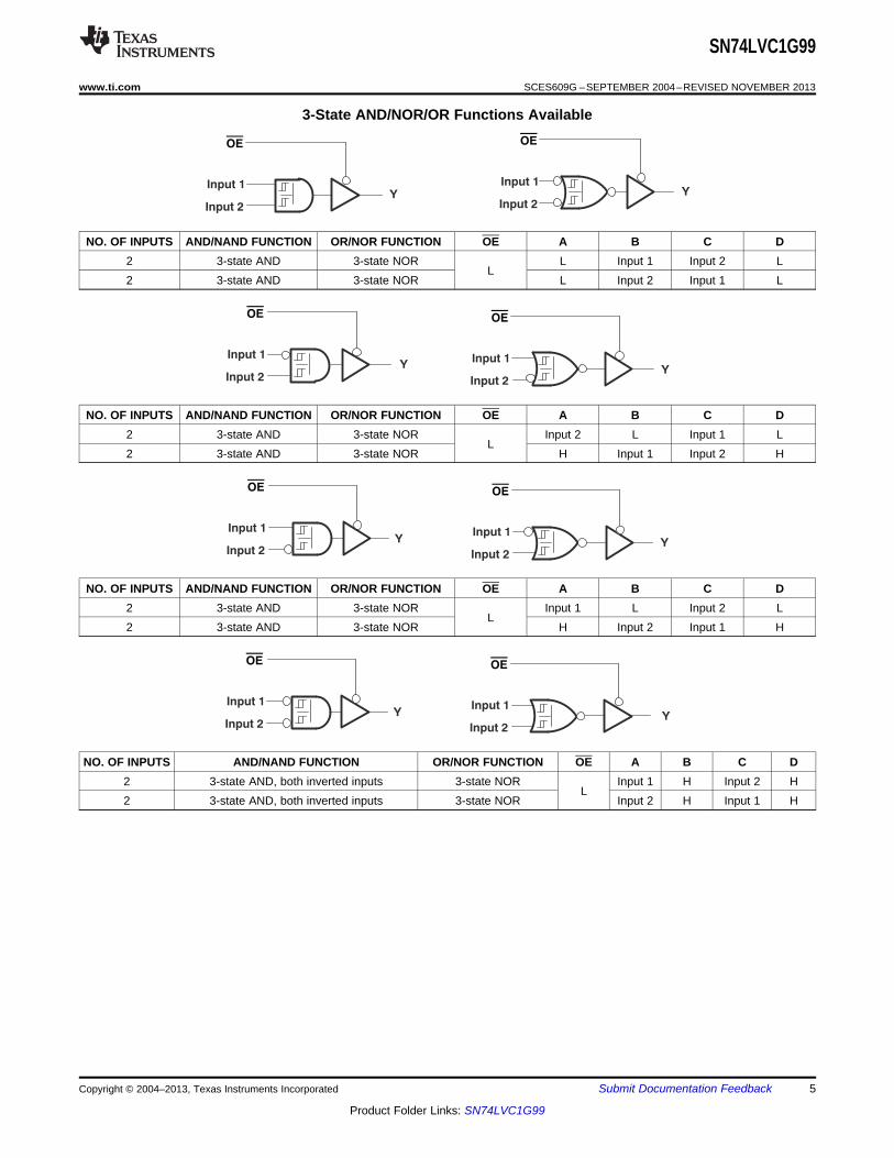
3-State AND/NOR/OR Functions Available
NO. OF INPUTS AND/NAND FUNCTION OR/NOR FUNCTION OE A B C D2 3-state AND 3-state NOR L Input 1 Input 2 L
L2 3-state AND 3-state NOR L Input 2 Input 1 L
NO. OF INPUTS AND/NAND FUNCTION OR/NOR FUNCTION OE A B C D2 3-state AND 3-state NOR Input 2 L Input 1 L
L2 3-state AND 3-state NOR H Input 1 Input 2 H
NO. OF INPUTS AND/NAND FUNCTION OR/NOR FUNCTION OE A B C D2 3-state AND 3-state NOR Input 1 L Input 2 L
L2 3-state AND 3-state NOR H Input 2 Input 1 H
NO. OF INPUTS AND/NAND FUNCTION OR/NOR FUNCTION OE A B C D2 3-state AND, both inverted inputs 3-state NOR Input 1 H Input 2 H
L2 3-state AND, both inverted inputs 3-state NOR Input 2 H Input 1 H
Copyright © 2004–2013, Texas Instruments Incorporated Submit Documentation Feedback 5
Product Folder Links: SN74LVC1G99

Input 1Y
Input 2
Input 1
Y
Input 2
OEOE
Input 1Y
Input 2
Input 1
Y
Input 2
OEOE
Input 1Y
Input 2
Input 1
Y
Input 2
OEOE
Input 1Y
Input 2
Input 1Y
Input 2
OE OE
SN74LVC1G99
SCES609G –SEPTEMBER 2004–REVISED NOVEMBER 2013 www.ti.com
3-State NAND/OR Functions Available
NO. OF INPUTS AND/NAND FUNCTION OR/NOR FUNCTION OE A B C D2 3-state NAND 3-state OR L Input 1 Input 2 H
L2 3-state NAND 3-state OR L Input 2 Input 1 H
NO. OF INPUTS AND/NAND FUNCTION OR/NOR FUNCTION OE A B C D2 3-state NAND 3-state OR Input 2 L Input 1 H
L2 3-state NAND 3-state OR H Input 1 Input 2 L
NO. OF INPUTS AND/NAND FUNCTION OR/NOR FUNCTION OE A B C D2 3-state NAND 3-state OR Input 1 L Input 2 H
L2 3-state NAND 3-state OR H Input 2 Input 1 L
NO. OF INPUTS AND/NAND FUNCTION OR/NOR FUNCTION OE A B C D2 3-state NAND 3-state OR Input 1 H Input 2 L
L2 3-state NAND 3-state OR Input 2 H Input 1 L
6 Submit Documentation Feedback Copyright © 2004–2013, Texas Instruments Incorporated
Product Folder Links: SN74LVC1G99

Input 1
YInput 2
OE
Input 1
YInput 2
OE
Input 1
YInput 2
OE
Input 1Y
Input 2
OE
SN74LVC1G99
www.ti.com SCES609G –SEPTEMBER 2004–REVISED NOVEMBER 2013
3-State XOR/XNOR Functions Available
FUNCTION OE A B C DInput 1 H or L L Input 2Input 2 H or L L Input 1H or L Input 1 H Input 2
3-state XOR LH or L Input 2 H Input 1
L H Input 1 Input 2L H Input 2 Input 1
FUNCTION OE A B C D3-state XOR L H L Input 1 Input 2
FUNCTION OE A B C D3-state XOR L H L Input 1 Input 2
FUNCTION OE A B C D3-state XNOR H L Input 1 Input 2
L3-state XNOR H L Input 2 Input 1
Copyright © 2004–2013, Texas Instruments Incorporated Submit Documentation Feedback 7
Product Folder Links: SN74LVC1G99

SN74LVC1G99
SCES609G –SEPTEMBER 2004–REVISED NOVEMBER 2013 www.ti.com
Absolute Maximum Ratings (1)
over operating free-air temperature range (unless otherwise noted)MIN MAX UNIT
VCC Supply voltage range –0.5 6.5 VVI Input voltage range (2) –0.5 6.5 VVO Voltage range applied to any output in the high-impedance or power-off state (2) –0.5 6.5 VVO Voltage range applied to any output in the high or low state (2) (3) –0.5 VCC + 0.5 VIIK Input clamp current VI < 0 –50 mAIOK Output clamp current VO < 0 –50 mAIO Continuous output current ±50 mA
Continuous current through VCC or GND ±100 mADCT package 220
θJA Package thermal impedance (4) DCU package 227 °C/WYZP package 102
Tstg Storage temperature range –65 150 °C
(1) Stresses beyond those listed under "absolute maximum ratings" may cause permanent damage to the device. These are stress ratingsonly, and functional operation of the device at these or any other conditions beyond those indicated under "recommended operatingconditions" is not implied. Exposure to absolute-maximum-rated conditions for extended periods may affect device reliability.
(2) The input and output negative voltage ratings may be exceeded if the input and output current ratings are observed.(3) The value of VCC is provided in the recommended operating conditions table.(4) The package thermal impedance is calculated in accordance with JESD 51-7.
Recommended Operating Conditions (1)
MIN MAX UNITOperating 1.65 5.5
VCC Supply voltage VData retention only 1.5
VI Input voltage 0 5.5 VVO Output voltage 0 VCC V
VCC = 1.65 V –4VCC = 2.3 V –8
IOH High-level output current –16 mAVCC = 3 V
–24VCC = 4.5 V –32VCC = 1.65 V 4VCC = 2.3 V 8
IOL Low-level output current 16 mAVCC = 3 V
24VCC = 4.5 V 32VCC = 1.8 V ± 0.15 V, 2.5 V ± 0.2 V 20
Δt/Δv Input transition rise or fall rate VCC = 3.3 V ± 0.3 V 10 ns/VVCC = 5 V ± 0.5 V 5
(1) All unused inputs of the device must be held at VCC or GND to ensure proper device operation. Refer to the TI application report,Implications of Slow or Floating CMOS Inputs, literature number SCBA004.
8 Submit Documentation Feedback Copyright © 2004–2013, Texas Instruments Incorporated
Product Folder Links: SN74LVC1G99

SN74LVC1G99
www.ti.com SCES609G –SEPTEMBER 2004–REVISED NOVEMBER 2013
Electrical Characteristicsover recommended operating free-air temperature range (unless otherwise noted)
–40°C to 85°C –40°C to 125°CPARAMETER TEST CONDITIONS VCC UNIT
MIN TYP (1) MAX MIN TYP (1) MAX
1.65 V 0.79 1.26 0.79 1.26
2.3 V 1.11 1.66 1.11 1.66VT+ Positive-going input 3 V 1.5 1.97 1.5 1.97 Vthresholdvoltage 4.5 V 2.16 2.84 2.16 2.84
5.5 V 2.61 3.43 2.61 3.43
1.65 V 0.39 0.72 0.39 0.72
2.3 V 0.58 0.97 0.58 0.97VT– Negative-going input 3 V 0.84 1.24 0.84 1.24 Vthresholdvoltage 4.5 V 1.41 1.89 1.41 1.89
5.5 V 1.87 2.39 1.87 2.39
1.65 V 0.37 0.72 0.37 0.72
2.3 V 0.48 0.87 0.48 0.87ΔVT Hysteresis 3 V 0.56 0.97 0.56 0.97 V(VT+ – VT–)
4.5 V 0.71 1.14 0.71 1.14
5.5 V 0.71 1.21 0.71 1.21
1.65 VIOH = –100 µA to VCC – 0.1 VCC – 0.1
5.5 V
IOH = –4 mA 1.65 V 1.2 1.2VOH VIOH = –8 mA 2.3 V 1.9 1.9
IOH = –16 mA 2.4 2.43 V
IOH = –24 mA 2.3 2.3
IOH = –32 mA 4.5 V 3.8 3.8
1.65 VIOL = 100 µA to 0.1 0.1
5.5 V
IOL = 4 mA 1.65 V 0.45 0.45VOL VIOL = 8 mA 2.3 V 0.3 0.3
IOL = 16 mA 0.4 0.43 V
IOL = 24 mA 0.55 0.55
IOL = 32 mA 4.5 V 0.55 0.55
0 V toII VI = 5.5 V or GND ±5 ±5 µA5.5 V
Ioff VI or VO = 5.5 V 0 V ±10 ±10 µA
1.65 VIOZ VO = VCC or GND to ±10 ±10 µA
5.5 V
1.65 VICC VI = 5.5 V or GND, IO = 0 to 10 10 µA
5.5 V
3 V toΔICC One input at VCC – 0.6 V, Other inputs at VCC or GND 500 500 µA5.5 V
Ci VI = VCC or GND 3.3 V 3.5 3.5 pF
Co VO = VCC or GND 3.3 V 6 6 pF
(1) TA = 25°C
Copyright © 2004–2013, Texas Instruments Incorporated Submit Documentation Feedback 9
Product Folder Links: SN74LVC1G99

SN74LVC1G99
SCES609G –SEPTEMBER 2004–REVISED NOVEMBER 2013 www.ti.com
Switching Characteristicsover recommended operating free-air temperature range, CL = 15 pF (unless otherwise noted) (see Figure 1)
SN74LVC1G99–40°C to 85°C
FROM TOPARAMETER VCC = 1.8 V VCC = 2.5 V VCC = 3.3 V VCC = 5 V UNIT(INPUT) (OUTPUT) ± 0.15 V ± 0.2 V ± 0.3 V ± 0.5 V
MIN MAX MIN MAX MIN MAX MIN MAX
A 4.5 30.1 2.5 11.3 1.8 7.5 1.3 4.8
B 4.4 28.3 2.4 10.8 1.8 7.2 1.3 4.7tpd Y ns
C 4.4 29.1 2.4 11.7 1.9 7.6 1.3 5
D 4.3 25.1 2.4 10.2 1.7 6.7 1.3 4.5
ten OE Y 3.4 24.7 2.1 10 1.3 5.8 1 3.8 ns
tdis OE Y 4 15.5 2.7 7.5 3.5 7 2 5.5 ns
Switching Characteristicsover recommended operating free-air temperature range, CL = 30 pF or 50 pF (unless otherwise noted) (see Figure 2)
SN74LVC1G99–40°C to 85°C
FROM TOPARAMETER VCC = 1.8 V VCC = 2.5 V VCC = 3.3 V VCC = 5 V UNIT(INPUT) (OUTPUT) ± 0.15 V ± 0.2 V ± 0.3 V ± 0.5 V
MIN MAX MIN MAX MIN MAX MIN MAX
A 4.6 30.8 2.6 11.7 2.4 8.4 1.8 5.5
B 4.6 28.9 2.6 11.3 2.3 8.2 1.8 5.4tpd Y ns
C 4.4 29.8 2.5 12.3 2.5 8.6 1.8 5.7
D 4.3 25.7 2.5 10.7 2.4 7.6 1.6 5.2
ten OE Y 4.2 25.2 2.4 11.3 2 7 1.7 4.7 ns
tdis OE Y 3.7 15 2 5.8 2.1 5.6 1 4.5 ns
Switching Characteristicsover recommended operating free-air temperature range (unless otherwise noted) (see Figure 2)
SN74LVC1G99–40°C to 125°C
FROM TOPARAMETER VCC = 1.8 V VCC = 2.5 V VCC = 3.3 V VCC = 5 V UNIT(INPUT) (OUTPUT) ± 0.15 V ± 0.2 V ± 0.3 V ± 0.5 V
MIN MAX MIN MAX MIN MAX MIN MAX
A 4.6 32.8 2.6 13.7 2.4 10.4 1.8 6.9
B 4.6 30.9 2.6 13.3 2.3 10.2 1.8 6.8tpd Y ns
C 4.4 31.8 2.4 14.3 2.5 10.6 1.8 7.2
D 4.3 27.7 2.5 12.7 2.4 9.5 1.6 6.5
ten OE Y 4.2 27.2 2.4 13.3 2.0 9.0 1.7 6.0 ns
tdis OE Y 3.7 17.0 2.0 7.3 2.1 7.4 1.0 5.6 ns
Operating CharacteristicsTA = 25°C
VCC = 1.8 V VCC = 2.5 V VCC = 3.3 V VCC = 5 VPARAMETER TEST CONDITIONS UNIT
TYP TYP TYP TYPCpd Power dissipation capacitance f = 10 MHz 19 20 22 27 pF
10 Submit Documentation Feedback Copyright © 2004–2013, Texas Instruments Incorporated
Product Folder Links: SN74LVC1G99

thtsu
From OutputUnder Test
C
(see Note A)L
LOAD CIRCUIT
S1
VLOAD
Open
GND
RL
Data Input
Timing Input
0 V
0 V0 V
tW
Input
0 VInput
OutputWaveform 1
S1 at V
(see Note B)LOAD
OutputWaveform 2
S1 at GND(see Note B)
VOL
VOH
0 V
»0 V
Output
Output
t /tPLH PHL Open
TEST S1
OutputControl
VM
VM VM
VM
VM
1.8 V 0.15 V±
2.5 V 0.2 V±
3.3 V 0.3 V±
5 V 0.5 V±
1 MW
1 MW
1 MW
1 MW
VCC RL
2 × VCC
2 × VCC
6 V
2 × VCC
VLOAD CL
15 pF
15 pF
15 pF
15 pF
0.15 V
0.15 V
0.3 V
0.3 V
VD
3 V
VI
VCC/2
VCC/2
1.5 V
VCC/2
VM
£2 ns
£2 ns
£2.5 ns
£2.5 ns
INPUTS
RL
t /tr f
VCC
VCC
VCC
VLOADt /tPLZ PZL
GNDt /tPHZ PZH
VOLTAGE WAVEFORMSENABLE AND DISABLE TIMES
LOW- AND HIGH-LEVEL ENABLING
VOLTAGE WAVEFORMSPROPAGATION DELAY TIMES
INVERTING AND NONINVERTING OUTPUTS
NOTES: A. C includes probe and jig capacitance.
B. Waveform 1 is for an output with internal conditions such that the output is low, except when disabled by the output control.Waveform 2 is for an output with internal conditions such that the output is high, except when disabled by the output control.
C. All input pulses are supplied by generators having the following characteristics: PRR 10 MHz, Z = 50 .
D. The outputs are measured one at a time, with one transition per measurement.E. t and t are the same as t .
F. t and t are the same as t .
G. t and t are the same as t .
H. All parameters and waveforms are not applicable to all devices.
L
O
PLZ PHZ dis
PZL PZH en
PLH PHL pd
£ W
VOLTAGE WAVEFORMSPULSE DURATION
VOLTAGE WAVEFORMSSETUP AND HOLD TIMES
VI
VI
VI
VM
VM
V /2LOAD
tPZL tPLZ
tPHZtPZH
V – VOH D
V + VOL D
VM
VM VM
VM
VOL
VOH
VI
VI
VOH
VOL
VM
VM
VM
VM
tPLH tPHL
tPLHtPHL
SN74LVC1G99
www.ti.com SCES609G –SEPTEMBER 2004–REVISED NOVEMBER 2013
Parameter Measurement Information
Figure 1. Load Circuit and Voltage Waveforms
Copyright © 2004–2013, Texas Instruments Incorporated Submit Documentation Feedback 11
Product Folder Links: SN74LVC1G99

thtsu
From OutputUnder Test
C
(see Note A)L
LOAD CIRCUIT
S1
VLOAD
Open
GND
RL
Data Input
Timing Input
0 V
0 V0 V
tW
Input
0 VInput
OutputWaveform 1
S1 at V
(see Note B)LOAD
OutputWaveform 2
S1 at GND(see Note B)
VOL
VOH
0 V
»0 V
Output
Output
TEST S1
t /tPLH PHL Open
OutputControl
VM
VM VM
VM
VM
1.8 V 0.15 V±
2.5 V 0.2 V±
3.3 V 0.3 V±
5 V 0.5 V±
1 kW
500 W
500 W
500 W
VCC RL
2 × VCC
2 × VCC
6 V
2 × VCC
VLOAD CL
30 pF
30 pF
50 pF
50 pF
0.15 V
0.15 V
0.3 V
0.3 V
VD
3 V
VI
VCC/2
VCC/2
1.5 V
VCC/2
VM
£2 ns
£2 ns
£2.5 ns
£2.5 ns
INPUTS
RL
t /tr f
VCC
VCC
VCC
VLOADt /tPLZ PZL
GNDt /tPHZ PZH
VOLTAGE WAVEFORMSENABLE AND DISABLE TIMES
LOW- AND HIGH-LEVEL ENABLING
VOLTAGE WAVEFORMSPROPAGATION DELAY TIMES
INVERTING AND NONINVERTING OUTPUTS
NOTES: A. C includes probe and jig capacitance.
B. Waveform 1 is for an output with internal conditions such that the output is low, except when disabled by the output control.Waveform 2 is for an output with internal conditions such that the output is high, except when disabled by the output control.
C. All input pulses are supplied by generators having the following characteristics: PRR 10 MHz, Z = 50 .
D. The outputs are measured one at a time, with one transition per measurement.E. t and t are the same as t .
F. t and t are the same as t .
G. t and t are the same as t .
H. All parameters and waveforms are not applicable to all devices.
L
O
PLZ PHZ dis
PZL PZH en
PLH PHL pd
£ W
VOLTAGE WAVEFORMSPULSE DURATION
VOLTAGE WAVEFORMSSETUP AND HOLD TIMES
VI
VI
VI
VM
VM
V /2LOAD
tPZL tPLZ
tPHZtPZH
V – VOH D
V + VOL D
VM
VM VM
VM
VOL
VOH
VI
VI
VOH
VOL
VM
VM
VM
VM
tPLH tPHL
tPLHtPHL
SN74LVC1G99
SCES609G –SEPTEMBER 2004–REVISED NOVEMBER 2013 www.ti.com
Parameter Measurement Information (continued)
Figure 2. Load Circuit and Voltage Waveforms
12 Submit Documentation Feedback Copyright © 2004–2013, Texas Instruments Incorporated
Product Folder Links: SN74LVC1G99

SN74LVC1G99
www.ti.com SCES609G –SEPTEMBER 2004–REVISED NOVEMBER 2013
REVISION HISTORY
Changes from Revision E (October 2007) to Revision F Page
• Changed document template from TIMS format to DocZone format. .................................................................................. 1• Changed 3-State Mux graphic to fix labeling error. .............................................................................................................. 4
Changes from Revision F (April 2011) to Revision G Page
• Updated document to new TI data sheet format. ................................................................................................................. 1• Updated Features. ................................................................................................................................................................ 1• Added ESD warning. ............................................................................................................................................................ 2• Updated operating temperature range. ................................................................................................................................. 8
Copyright © 2004–2013, Texas Instruments Incorporated Submit Documentation Feedback 13
Product Folder Links: SN74LVC1G99
PACKAGE OPTION ADDENDUM
www.ti.com 13-Jun-2014
Addendum-Page 1
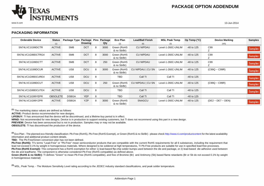
PACKAGING INFORMATION
Orderable Device Status(1)
Package Type PackageDrawing
Pins PackageQty
Eco Plan(2)
Lead/Ball Finish(6)
MSL Peak Temp(3)
Op Temp (°C) Device Marking(4/5)
Samples
SN74LVC1G99DCTR ACTIVE SM8 DCT 8 3000 Green (RoHS& no Sb/Br)
CU NIPDAU Level-1-260C-UNLIM -40 to 125 C99Z
SN74LVC1G99DCTRG4 ACTIVE SM8 DCT 8 3000 Green (RoHS& no Sb/Br)
CU NIPDAU Level-1-260C-UNLIM -40 to 125 C99Z
SN74LVC1G99DCTT ACTIVE SM8 DCT 8 250 Green (RoHS& no Sb/Br)
CU NIPDAU Level-1-260C-UNLIM -40 to 125 C99Z
SN74LVC1G99DCUR ACTIVE US8 DCU 8 3000 Green (RoHS& no Sb/Br)
CU NIPDAU | CU SN Level-1-260C-UNLIM -40 to 125 (C99Q ~ C99R)
SN74LVC1G99DCURE4 ACTIVE US8 DCU 8 TBD Call TI Call TI -40 to 125
SN74LVC1G99DCUT ACTIVE US8 DCU 8 250 Green (RoHS& no Sb/Br)
CU NIPDAU | CU SN Level-1-260C-UNLIM -40 to 125 (C99Q ~ C99R)
SN74LVC1G99DCUTE4 ACTIVE US8 DCU 8 TBD Call TI Call TI -40 to 125
SN74LVC1G99YEPR OBSOLETE DSBGA YEP 8 TBD Call TI Call TI -40 to 125
SN74LVC1G99YZPR ACTIVE DSBGA YZP 8 3000 Green (RoHS& no Sb/Br)
SNAGCU Level-1-260C-UNLIM -40 to 125 (DE2 ~ DE7 ~ DEN)
(1) The marketing status values are defined as follows:ACTIVE: Product device recommended for new designs.LIFEBUY: TI has announced that the device will be discontinued, and a lifetime-buy period is in effect.NRND: Not recommended for new designs. Device is in production to support existing customers, but TI does not recommend using this part in a new design.PREVIEW: Device has been announced but is not in production. Samples may or may not be available.OBSOLETE: TI has discontinued the production of the device.
(2) Eco Plan - The planned eco-friendly classification: Pb-Free (RoHS), Pb-Free (RoHS Exempt), or Green (RoHS & no Sb/Br) - please check http://www.ti.com/productcontent for the latest availabilityinformation and additional product content details.TBD: The Pb-Free/Green conversion plan has not been defined.Pb-Free (RoHS): TI's terms "Lead-Free" or "Pb-Free" mean semiconductor products that are compatible with the current RoHS requirements for all 6 substances, including the requirement thatlead not exceed 0.1% by weight in homogeneous materials. Where designed to be soldered at high temperatures, TI Pb-Free products are suitable for use in specified lead-free processes.Pb-Free (RoHS Exempt): This component has a RoHS exemption for either 1) lead-based flip-chip solder bumps used between the die and package, or 2) lead-based die adhesive used betweenthe die and leadframe. The component is otherwise considered Pb-Free (RoHS compatible) as defined above.Green (RoHS & no Sb/Br): TI defines "Green" to mean Pb-Free (RoHS compatible), and free of Bromine (Br) and Antimony (Sb) based flame retardants (Br or Sb do not exceed 0.1% by weightin homogeneous material)
(3) MSL, Peak Temp. - The Moisture Sensitivity Level rating according to the JEDEC industry standard classifications, and peak solder temperature.

PACKAGE OPTION ADDENDUM
www.ti.com 13-Jun-2014
Addendum-Page 2
(4) There may be additional marking, which relates to the logo, the lot trace code information, or the environmental category on the device.
(5) Multiple Device Markings will be inside parentheses. Only one Device Marking contained in parentheses and separated by a "~" will appear on a device. If a line is indented then it is a continuationof the previous line and the two combined represent the entire Device Marking for that device.
(6) Lead/Ball Finish - Orderable Devices may have multiple material finish options. Finish options are separated by a vertical ruled line. Lead/Ball Finish values may wrap to two lines if the finishvalue exceeds the maximum column width.
Important Information and Disclaimer:The information provided on this page represents TI's knowledge and belief as of the date that it is provided. TI bases its knowledge and belief on informationprovided by third parties, and makes no representation or warranty as to the accuracy of such information. Efforts are underway to better integrate information from third parties. TI has taken andcontinues to take reasonable steps to provide representative and accurate information but may not have conducted destructive testing or chemical analysis on incoming materials and chemicals.TI and TI suppliers consider certain information to be proprietary, and thus CAS numbers and other limited information may not be available for release.
In no event shall TI's liability arising out of such information exceed the total purchase price of the TI part(s) at issue in this document sold by TI to Customer on an annual basis.
OTHER QUALIFIED VERSIONS OF SN74LVC1G99 :
• Automotive: SN74LVC1G99-Q1
NOTE: Qualified Version Definitions:
• Automotive - Q100 devices qualified for high-reliability automotive applications targeting zero defects
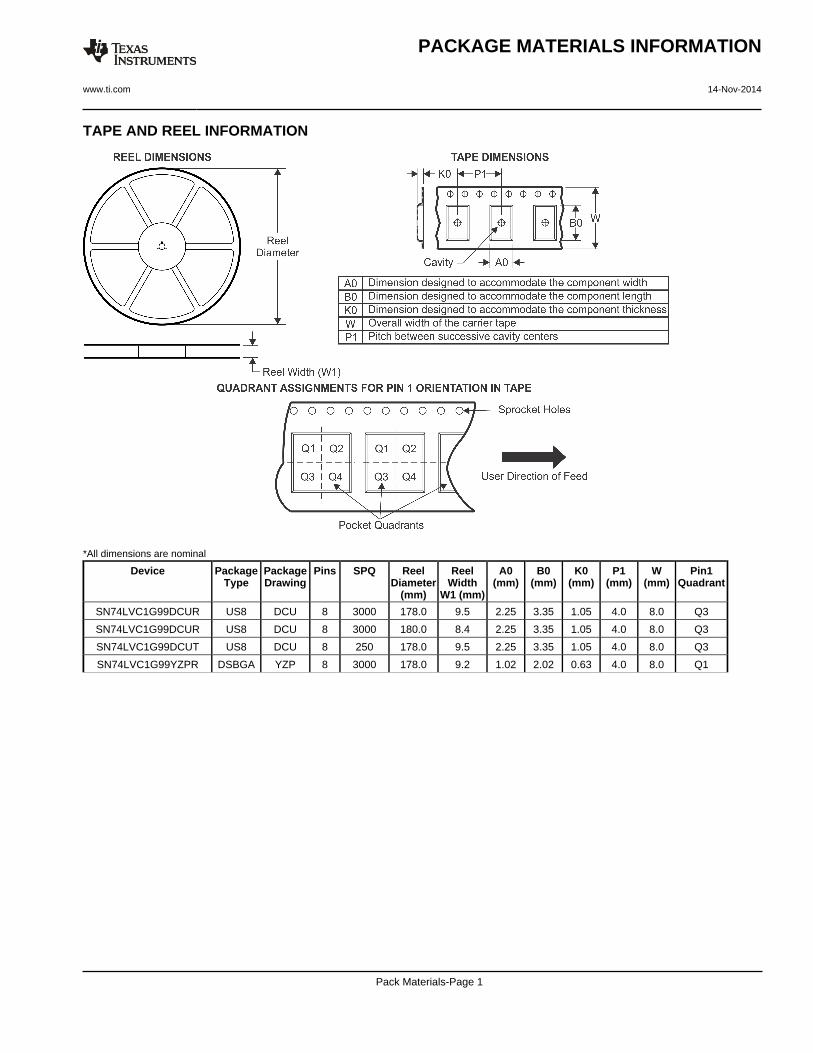
TAPE AND REEL INFORMATION
*All dimensions are nominal
Device PackageType
PackageDrawing
Pins SPQ ReelDiameter
(mm)
ReelWidth
W1 (mm)
A0(mm)
B0(mm)
K0(mm)
P1(mm)
W(mm)
Pin1Quadrant
SN74LVC1G99DCUR US8 DCU 8 3000 178.0 9.5 2.25 3.35 1.05 4.0 8.0 Q3
SN74LVC1G99DCUR US8 DCU 8 3000 180.0 8.4 2.25 3.35 1.05 4.0 8.0 Q3
SN74LVC1G99DCUT US8 DCU 8 250 178.0 9.5 2.25 3.35 1.05 4.0 8.0 Q3
SN74LVC1G99YZPR DSBGA YZP 8 3000 178.0 9.2 1.02 2.02 0.63 4.0 8.0 Q1
PACKAGE MATERIALS INFORMATION
www.ti.com 14-Nov-2014
Pack Materials-Page 1

*All dimensions are nominal
Device Package Type Package Drawing Pins SPQ Length (mm) Width (mm) Height (mm)
SN74LVC1G99DCUR US8 DCU 8 3000 202.0 201.0 28.0
SN74LVC1G99DCUR US8 DCU 8 3000 202.0 201.0 28.0
SN74LVC1G99DCUT US8 DCU 8 250 202.0 201.0 28.0
SN74LVC1G99YZPR DSBGA YZP 8 3000 220.0 220.0 35.0
PACKAGE MATERIALS INFORMATION
www.ti.com 14-Nov-2014
Pack Materials-Page 2

MECHANICAL DATA
MPDS049B – MAY 1999 – REVISED OCTOBER 2002
POST OFFICE BOX 655303 • DALLAS, TEXAS 75265
DCT (R-PDSO-G8) PLASTIC SMALL-OUTLINE PACKAGE
ÇÇÇÇÇÇÇÇÇÇÇÇÇÇÇÇÇÇÇÇ
0,600,20
0,25
0° – 8°
0,15 NOM
Gage Plane
4188781/C 09/02
4,25
5
0,300,15
2,903,752,70
8
4
3,152,75
1
0,100,00
1,30 MAX
Seating Plane
0,10
M0,130,65
PIN 1INDEX AREA
NOTES: A. All linear dimensions are in millimeters.B. This drawing is subject to change without notice.C. Body dimensions do not include mold flash or protrusionD. Falls within JEDEC MO-187 variation DA.


D: Max =
E: Max =
1.918 mm, Min =
0.918 mm, Min =
1.858 mm
0.858 mm


IMPORTANT NOTICETexas Instruments Incorporated and its subsidiaries (TI) reserve the right to make corrections, enhancements, improvements and otherchanges to its semiconductor products and services per JESD46, latest issue, and to discontinue any product or service per JESD48, latestissue. Buyers should obtain the latest relevant information before placing orders and should verify that such information is current andcomplete. All semiconductor products (also referred to herein as “components”) are sold subject to TI’s terms and conditions of salesupplied at the time of order acknowledgment.TI warrants performance of its components to the specifications applicable at the time of sale, in accordance with the warranty in TI’s termsand conditions of sale of semiconductor products. Testing and other quality control techniques are used to the extent TI deems necessaryto support this warranty. Except where mandated by applicable law, testing of all parameters of each component is not necessarilyperformed.TI assumes no liability for applications assistance or the design of Buyers’ products. Buyers are responsible for their products andapplications using TI components. To minimize the risks associated with Buyers’ products and applications, Buyers should provideadequate design and operating safeguards.TI does not warrant or represent that any license, either express or implied, is granted under any patent right, copyright, mask work right, orother intellectual property right relating to any combination, machine, or process in which TI components or services are used. Informationpublished by TI regarding third-party products or services does not constitute a license to use such products or services or a warranty orendorsement thereof. Use of such information may require a license from a third party under the patents or other intellectual property of thethird party, or a license from TI under the patents or other intellectual property of TI.Reproduction of significant portions of TI information in TI data books or data sheets is permissible only if reproduction is without alterationand is accompanied by all associated warranties, conditions, limitations, and notices. TI is not responsible or liable for such altereddocumentation. Information of third parties may be subject to additional restrictions.Resale of TI components or services with statements different from or beyond the parameters stated by TI for that component or servicevoids all express and any implied warranties for the associated TI component or service and is an unfair and deceptive business practice.TI is not responsible or liable for any such statements.Buyer acknowledges and agrees that it is solely responsible for compliance with all legal, regulatory and safety-related requirementsconcerning its products, and any use of TI components in its applications, notwithstanding any applications-related information or supportthat may be provided by TI. Buyer represents and agrees that it has all the necessary expertise to create and implement safeguards whichanticipate dangerous consequences of failures, monitor failures and their consequences, lessen the likelihood of failures that might causeharm and take appropriate remedial actions. Buyer will fully indemnify TI and its representatives against any damages arising out of the useof any TI components in safety-critical applications.In some cases, TI components may be promoted specifically to facilitate safety-related applications. With such components, TI’s goal is tohelp enable customers to design and create their own end-product solutions that meet applicable functional safety standards andrequirements. Nonetheless, such components are subject to these terms.No TI components are authorized for use in FDA Class III (or similar life-critical medical equipment) unless authorized officers of the partieshave executed a special agreement specifically governing such use.Only those TI components which TI has specifically designated as military grade or “enhanced plastic” are designed and intended for use inmilitary/aerospace applications or environments. Buyer acknowledges and agrees that any military or aerospace use of TI componentswhich have not been so designated is solely at the Buyer's risk, and that Buyer is solely responsible for compliance with all legal andregulatory requirements in connection with such use.TI has specifically designated certain components as meeting ISO/TS16949 requirements, mainly for automotive use. In any case of use ofnon-designated products, TI will not be responsible for any failure to meet ISO/TS16949.Products ApplicationsAudio www.ti.com/audio Automotive and Transportation www.ti.com/automotiveAmplifiers amplifier.ti.com Communications and Telecom www.ti.com/communicationsData Converters dataconverter.ti.com Computers and Peripherals www.ti.com/computersDLP® Products www.dlp.com Consumer Electronics www.ti.com/consumer-appsDSP dsp.ti.com Energy and Lighting www.ti.com/energyClocks and Timers www.ti.com/clocks Industrial www.ti.com/industrialInterface interface.ti.com Medical www.ti.com/medicalLogic logic.ti.com Security www.ti.com/securityPower Mgmt power.ti.com Space, Avionics and Defense www.ti.com/space-avionics-defenseMicrocontrollers microcontroller.ti.com Video and Imaging www.ti.com/videoRFID www.ti-rfid.comOMAP Applications Processors www.ti.com/omap TI E2E Community e2e.ti.comWireless Connectivity www.ti.com/wirelessconnectivity
Mailing Address: Texas Instruments, Post Office Box 655303, Dallas, Texas 75265Copyright © 2014, Texas Instruments Incorporated