ULSI Process Integration II - Princeton University
17
ULSI PROCESS INTEGRATION II
Transcript of ULSI Process Integration II - Princeton University

ULSI PROCESS INTEGRATION II
ULSI PROCESS INTEGRATION II
Proceedings ofthe International Symposium
Editors
C. L. Claeys
IMEC
Leuven, Belgium
F. Gonzalez
Micron Technology, Inc.
Boise, Idaho, USA
J. Murota
Tohoku University
Sendai, Japan
K. Saraswat
Stanford University
Stanford, California, USA
ELECTRONICS DIVISION
Proceedings Volume 2001-2
THE ELECTROCHEMICAL SOCIETY, INC.
65 South Main St., Pennington, NJ 08534-2839, USA
Copyright 2001 by The Electrochemical Society, Inc.
All rights reserved.
This book has been registered with Copyright Clearance Center, Inc.
For further information, please contact the Copyright Clearance Center,
Salem, Massachusetts.
Published by:
The Electrochemical Society, Inc.
65 South Main Street
Pennington, New Jersey 08534-2839, USA
Telephone 609.737.1902
Fax 609.737.2743
e-mail: [email protected]
Web: http://www.electrochem.org
Library of Congress Catalogue Number: 00-112102
ISBN 1-56677-308-3
Printed in the United States of America
CONFERENCE CHAIRMEN
Cor Claeys
IMEC,
Leuven, Belgium
Fernando Gonzalez
Micron Technology, Inc.
Boise, ID, U.S.A.
Junichi Murota
Tohoku University
Aoba-Ku, Sendai, Japan
Khrisna Saraswat
Stanford University
Stanford, CA, U.S.A.
TECHICAL PROGRAM COMMITTEE
Varian
U.S.A.
Hisayo Sasaki Momose
TOSHIBA Corp
Yokohama, Japan
Gary I
IBM Microelectronics
Hopewell Junction, NY, U.S.A.
Osaka University
Suita, Osaka, Japan
T.
Lucent Technologies
Murray Hill, NJ, U.S.A.
NEC Corporation
Shimokuzawa, Sagamihara, Japan
Richard Fair
Duke University
Durham, NC, U.S.A.
Carl Osburn
North Carolina State University
Raleigh, NC, U.S.A.
Mart Graef
Philips Research
Eindhoven, The Netherlands
Hiroshi Onoda
Oki Electronic Industry Co. Ltd.
Hachioji, Tokyo, Japan
Yoshio Homma
Hitachi Ltd.
Kokubunji, Japan
Nobuo Sasaki
Fujitsu Laboratories Ltd.,
Morinosato-Wakamiya, Atsugi,
Hiroshi Iwai
Tokyo Institute of Technology
Yo!
Krishna Shenai
University of Illinois
Chicago, IL, U.S.A.
Hisham Massoud
Duke University
Durham, NC, U.S.A.
Shi-Chung Sun
Wafertech
Comas, WA, U.S.A.
Mitsubishi Electric Co.
Itami, Hyogo, Japan
Shigeaki Zaima
Nagoya University
Chikusa-ku, Nagoya, Japan
This One
AA6W-W5X-HSUH
PREFACE
The first international Symposium on ULSI Process was initially organized in
Honolulu, Hawaii in 1999. The following Proceedings Volume contains papers that
were presented at the second international symposium on ULSI Process Integration,
held in Washington D.C. on March 24-31, 2001 as part of the 199th Meeting of the
Electrochemical Society. The symposium was well rounded with a collection of 52
papers within 56 presentations. The presentations of the enclosed papers were
scheduled Monday through Thursday which covered the entire length of the
conference with a wide range of process integration and IC device applications.
The main focus of the ULSI Process Integration symposium was to provide an
international forum on topics related to the interrelationships and interactions between
multi-process steps. The unit process applications are taken a step further by
considering the overall effects to the whole applied process. The single process steps
were studied in the context of the formation of an electrical device. The program
focused on recent innovations in ULSI scaling of devices, on transistor process
technology, on defect impacts on process integration and on novel processes.
The ULSI Process Integration Symposium was sponsored by the Electronics
Division of the Electrochemical Society and by the Electron Devices Society of the
IEEE. The symposium was international in scope and included authors Belgium,
France, Germany, India, Japan, Korea, Singapore and United States. This proceedings
contains 52 papers, including 5 keynote speakers, 28 invited speakers and 19
contributing speakers. The symposium consisted of seven sections focusing on
Process Integration and Device Scaling, Process Integration and Device
Performance, Process Integration of Si-Ge Technologies, FEOL Process
Integration of Transistor Devices, Process Integration and Defect Interactions,
Process Integration in Circuit Applications, Substrate Integration Using SOI, and
FEOL Process Integration and Unit Processes.
The Process Integration function has been a crucial engineering activity to the
semiconductor development. Process Integration has used many unit process within a
multi-process sequence to make them function properly within the ULSI electrical
device. The process and device scaling highlighted in the keynote address by Dr. Iwai
outlined the future problems in scaling below 100 nm feature size. He cited the
process integration of some new materials and some novel devices that are needed to
enable the ULSI devices below the sub 100 nm level. In the Full process integration
section, Dr. Ishitani discussed the role of different photolithography techniques that
would be useful in the 0. 1 urn devices. The FEOL process integration section focused
primarily on the gate stack and transistor integration like Dr. Huffs key note
presentation that gave an excellent picture of the issues in the gate stack formation.
The talk on "Silicon Germanium Trends on Process Integration" by Dr. Kasper
summarized the roadmap of the SiGe development. The role of defects in integration
from silicon metals to dislocations were highlighted by the section on Defects and
Process Integration. Substrate Integration emphasis was focused on SOI tpoics.
Finally, unit process development that may represent good concepts for future process
integration were reviewed in the last section.
v
The DIELECTRIC SCIENCE AND TECHNOLOGY DIVISION T.D.
CALLINAN AWARD ADDRESS on the "Evolution of the Metallization Concepts
for Applications in the Integrated Circuits" was given by S.P. Murarka from
Rensselaer Polytechnic Institute and is included in the Proceedings.
The organizers would like to thank the members of the technical program
committee and all the authors for the on-time submission of their manuscripts. The
invited speakers are acknowledged for making this symposium possible by sharing their
perspectives and insights and by putting considerable effort in the preparation of the
camera-ready manuscripts. We want to acknowledge the contribution of the Session
chairmen in chairing the sessions. We also thank the staff of the Electrochemical
Society for their support.
November 2000 C.L.Claeys
F. Gonzalez
J.Murota
K. Saraswat
vt
Technologies for Large-Area Electronics on Deformable Substrates
J.C. Sturm, P.I. Hsu, M. Huang, H. Gleskova, S. Miller, A. Darhuber, S. Wagner, Z. Suo,
and S. Troian
Center for Photonics and Optoelectronic Materials (POEM), Princeton University,
Princeton, NJ 08544 USA
609-258-5610, 609-258-1954, [email protected]
Abstract
For large-area electronics to have an increasingly large-impact on consumer
applications, flexible substrate technology and lower cost patterning technologies must be
developed. In this paper, the mechanics of rolling and deforming thin foil substrates in
two and three dimensions are discussed. The impact of such deformations on
semiconductor devices and materials are presented. The effects of cylindrical
deformation can be mitigated by using thin substrates, but spherical deformation requires
device islands on soft substrates. For pattern formation, the transfer of ink down to a
feature size of the order of microns has been demonstrated using a modified version of
offset printing. While there are several practical issues which must be addressed, such as
ink stability while drying, it appears possible to scale such printing to the micron scale
and below.
Introduction
The conventional goal of the semiconductor industry is to make things small.
However, there is an emerging market for large-area electronics, or "macroelectronics,"
where the product must be large by definition. These applications are generally driven by
real world interfaces such as flat panel displays, large-area sensor arrays (e.g. X-ray
imaging plates), MEMS arrays, etc. Current generations of these products are made on
glass substrates using amorphous or polycrystalline semiconductor technology (typically
amorphous or polycrystalline silicon). For future products, it is highly desirable that they
be lightweight, flexible, and rugged. Furthermore, the drastic reduction of cost per unit
area of these products is difficult as long as they are made with standard photolithography
and etching. This paper will discuss two issues: novel substrate approaches and the
mechanics to develop flexible and even three-dimensional surfaces, and the scaling of
offset printing technology to small feature sizes.
Reliable and Deformable Substrates
Cylindrical Deformation
The most common amorphous silicon (a-Si) TFT's are made on glass substrates
with a maximum process temperature of 300 - 350 °C. For lightweight flexible
electronics, over the past few years many groups have developed a-Si TFT's on plastic
(e.g. polyimide) substrates with a maximum process temperature of 110-200 °C [1-6], or
506 Electrochemical Society Proceedings Volume 2001-2

even on stainless steel foil substrates (e.g 3 - 200 u,m thick) [7,8]. For processing on
stainless steel foil substrates, a planarizing and insulating oxide must first be deposited,
but after that step processing is much more straightforward for a-Si TFT's than that on
plastic. For example, there are no concerns about outgassing in vacuum systems,
shrinkage (as with plastic), allowable process temperature, etc. Polysilicon TFT's with
process temperatures of 950 °C have been successfully fabricated on steel foils [8]. The
results described in the rest of this section of the paper are from amorphous silicon (a-Si)
TFT's with a bottom gate, back-channel etch structure. After conventional fabrication on
flat substrates, individual transistors were stressed mechanically by deforming the
substrate in a cylindrical shape by bending it around a small diameter metal cylinder,
whose radius was varied as low as 0.5 mm (Fig. 1).
When a thin film substrate is cylindrically deformed, the inside surface of the foil is
in compression and the outside surface is in tension. If the mechanical stiffness of the
TFT layers on the surface is small compared to that of the substrate [9], it is well known
that for a radius of curvature p, the magnitude of the strain 8 on the two surfaces is
e = t/2p (1)
where t is the thickness of the foil. In the middle of the foil is a so-called "neutral plane"
where the strain is zero. Note that the strain in the surface layers, which will lead to
failure of the devices made in these layers, can be reduced simply by reducing the
substrate thickness. Because of the relatively small strains caused in these experiments
(typically < 0.01), there was relatively little plastic flow in the substrates during
deformation. The TFT's on both the stainless steel and polyimide substrates were
measured both after fabrication and after being released from the cylindrical deformation.
For TFT's on 25-nm stainless steel substrates, there was little change in their parameters
for bending down to radii of 2.5 mm, corresponding to a surface strain of 0.5% [10]. For
tighter radii of curvature, the TFT's failed before a noticeable shift in their characteristics
was observed, with a typical failure mode being delamination of the TFT structure from
the passivating oxide on the steel.
TFT's were also fabricated on 25-nm polyimide (Kapton E) substrates. In this case,
the soft plastic substrate is "compliant," so the neutral plane shifts towards the TFT
surface. This substantially reduces the strain in the TFT layer [11]. Fig 2 shows the
change in transistor parameters of maximum on current, leakage current, threshold
voltage, and field effect mobility in saturation after deformation, normalized by their
respective values before deformation. When the TFT's were on the inward side of the
foil, so that they were under compression, no change in characteristics was observed
when the TFT's were deformed to a radius of 0.5 mm (corresponding to a surface strain
of 2.2%) and released after one minute. When the TFT's were on the outside of the foil
(under tension), a noticeable change was already observed at a strain of 0.5% (radius of ~
2 mm). In this case the TFT film was beginning to crack, with the cracks running
perpendicular to the strain direction, presumably as a strain release mechanism (Fig. 3).
Up to a strain of 0.5%, however, no change in device characteristics was observed.
Electrochemical Society Proceedings Volume 2001-2 507
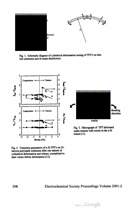
Fig. 1. Schematic diagram of cylindrical deformation testing of TFT's on thin
foil substrates and of strain distribution.
Compression * Tension
-3 -2 -1 1
. " . i - .
; Compression .* ■ *. Tension
A. ...IK
▲
?
5
— 1 lending^ a a Ci/
cracks
Fig. 3. Micrograph of TFT deformed
under tension with cracks in the a-Si
island [11].
Strain (%)
Fig. 2. Transistor parameters of a-Si TFT's on 25-
micron polyimide substrates after one minute of
cylindrical deformation and release, normalized to
their values before deformation [11].
508 Electrochemical Society Proceedings Volume 2001-2
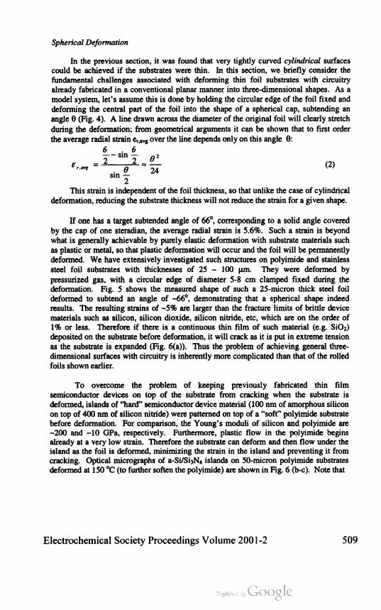
Spherical Deformation
In the previous section, it was found that very tightly curved cylindrical surfaces
could be achieved if the substrates were thin. In this section, we briefly consider the
fundamental challenges associated with deforming thin foil substrates with circuitry
already fabricated in a conventional planar manner into three-dimensional shapes. As a
model system, let's assume this is done by holding the circular edge of the foil fixed and
deforming the central part of the foil into the shape of a spherical cap, subtending an
angle 8 (Fig. 4). A line drawn across the diameter of the original foil will clearly stretch
during the deformation; from geometrical arguments it can be shown that to first order
the average radial strain er,aVg over the line depends only on this angle 9:
6 . 6— -sin — „ 2
E = 2 L „ t- (2)
sin —
2
This strain is independent of the foil thickness, so that unlike the case of cylindrical
deformation, reducing the substrate thickness will not reduce the strain for a given shape.
If one has a target subtended angle of 66°, corresponding to a solid angle covered
by the cap of one steradian, the average radial strain is 5.6%. Such a strain is beyond
what is generally achievable by purely elastic deformation with substrate materials such
as plastic or metal, so that plastic deformation will occur and the foil will be permanently
deformed. We have extensively investigated such structures on polyimide and stainless
steel foil substrates with thicknesses of 25 - 100 u,m. They were deformed by
pressurized gas, with a circular edge of diameter 5-8 cm clamped fixed during the
deformation. Fig. 5 shows the measured shape of such a 25-micron thick steel foil
deformed to subtend an angle of ~66°, demonstrating that a spherical shape indeed
results. The resulting strains of -5% are larger than the fracture limits of brittle device
materials such as silicon, silicon dioxide, silicon nitride, etc, which are on the order of
1% or less. Therefore if there is a continuous thin film of such material (e.g. SiO2>
deposited on the substrate before deformation, it will crack as it is put in extreme tension
as the substrate is expanded (Fig. 6(a)). Thus the problem of achieving general three-
dimensional surfaces with circuitry is inherently more complicated than that of the rolled
foils shown earlier.
To overcome the problem of keeping previously fabricated thin film
semiconductor devices on top of the substrate from cracking when the substrate is
deformed, islands of "hard" semiconductor device material (100 nm of amorphous silicon
on top of 400 nm of silicon nitride) were patterned on top of a "soft" polyimide substrate
before deformation. For comparison, the Young's moduli of silicon and polyimide are
~200 and -10 GPa, respectively. Furthermore, plastic flow in the polyimide begins
already at a very low strain. Therefore the substrate can deform and then flow under the
island as the foil is deformed, minimizing the strain in the island and preventing it from
cracking. Optical micrographs of a-Si/Si3N4 islands on 50-micron polyimide substrates
deformed at 150 °C (to further soften the polyimide) are shown in Fig. 6 (b-c). Note that
Electrochemical Society Proceedings Volume 2001-2 509

deformed
initial foi
20 40 60 80
Field of view (degree)
(b)
6.0 cm
Fig. 5. Stainless steel foil after deformation by
gas pressure, and measured shape of height vs.
radius.
Fig.4. (a) Schematic diagram of foil
deformation into a spherical cap, and ( b)
average radial strain across the foil after
deformation as a function of the field of view
e).
100 urn
(a)
Fig. 6. Micrographs after spherical deformation to -65° field of view of (a)
unpatterned 0.5 micron of Si02 on 25-nm stainless steel foil, (b) 400 nm Si3N4/100
nm a-Si on 50-um polyimide foil patterned to a ~120-um island, and (c) the same
layer structure as (b) patterned to a -75-u,m island.
510 Electrochemical Society Proceedings Volume 2001-2

Fig.7. Yield of device islands
without cracks after deformation
to -65° field of view, as a
function of island size. The
island stack was 400 nm
Si3N„/100 nm a-Si on 50-um
polyimide foil.
Island slze(um)
small islands (-70 microns across in this example) survive without cracking, while larger
islands (e.g. 150 microns) accumulate more strain and do crack [12]. Fig. 7 further
confirms this trend by showing the "yield" of crack-free islands after deformation as a
function of island size. Islands of size < 50 microns have nearly 100% yield, while for
sizes of 80 microns or larger the yield is near zero. Comparing the experimental results
to modeling, one finds that the islands begin to fail when the highest strain in them is
about -0.5 - 0.7% [12]. Note that the intermediate yield for intermediate sizes implies
some variation in substrate parameters (causing a variation in the island strain), or a
variation in the strain at which the islands crack, implying a failure mechanism related to
defects or imperfections. This is under further investigation.
Offset printing of UV-curable polymers
The microelectronics industry is continuously pushing to reduce the minimum
feature size of electronic devices. While this trend has drastically reduced the cost per
feature, the cost per unit area of substrate has not been reduced. For large area
electronics, the inherently large nature of the product does not allow one to reduce the
cost by shrinking as in the conventional microelectronics industry. Therefore many
groups are today exploring printing techniques such as gravure and offset printing, screen
printing, inkjet-printing and micro-contact printing for lithography or direct deposition of
patterned semiconductor- or polymer-based TFTs and LEDs [13-23]. The central goal of
this work is to reduce the cost of pattern formation of electronic products over large
areas.
The ultimate in low cost is conventional wet-printing, as used in newsprint,
magazines, etc. Therefore we have tried to scale conventional offset printing down to the
micron size range. This wet printing technique involves transferring liquid inks from a
flat and chemically patterned surface onto an unpatterned target substrate [24-27]. As
suggested by Fig. 8, there are four technological issues that arise in this process: (1)
fabrication of printing plates, (2) deposition and distribution of ink on the plates for
pattern definition, (3) rheological and surface control of ink patterns during printing, and
(4) rapid stabilization of printed patterns.
Electrochemical Society Proceedings Volume 2001-2 511
► l urn tun <
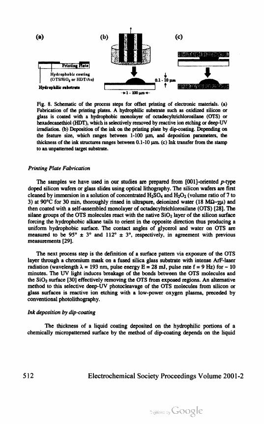
Fig. 8. Schematic of the process steps for offset printing of electronic materials, (a)
Fabrication of the printing plates. A hydrophilic substrate such as oxidized silicon or
glass is coated with a hydrophobic monolayer of octadecyltrichlorosilane (OTS) or
hexadecanethiol (HDT), which is selectively removed by reactive ion etching or deep-UV
irradiation, (b) Deposition of the ink on the printing plate by dip-coating. Depending on
the feature size, which ranges between 1-100 nm, and deposition parameters, the
thickness of the ink structures ranges between 0.1-10 um. (c) Ink transfer from the stamp
to an unpatterned target substrate.
Printing Plate Fabrication
The samples we have used in our studies are prepared from [001]-oriented p-type
doped silicon wafers or glass slides using optical lithography. The silicon wafers are first
cleaned by immersion in a solution of concentrated H2SO4 and H2O2 (volume ratio of 7 to
3) at 90°C for 30 min, thoroughly rinsed in ultrapure, deionized water (18 MQ-xn) and
then coated with a self-assembled monolayer of octadecyltrichlorosilane (OTS) [28]. The
silane groups of the OTS molecules react with the native SiO2 layer of the silicon surface
forcing the hydrophobic alkane tails to orient in the opposite direction thus producing a
uniform hydrophobic surface. The contact angles of glycerol and water on OTS are
measured to be 95° ± 3° and 112° ± 3°, respectively, in agreement with previous
measurements [29].
The next process step is the definition of a surface pattern via exposure of the OTS
layer through a chromium mask on a fused silica glass substrate with intense ArF-laser
radiation (wavelength X = 193 nm, pulse energy E = 28 mJ, pulse rate f = 9 Hz) for ~ 10
minutes. The UV light induces breakage of the bonds between the OTS molecules and
the Si02 surface [30] effectively removing the OTS from exposed regions. An alternative
method to this selective deep-UV photocleavage of the OTS molecules from silicon or
glass surfaces is reactive ion etching with a low-power oxygen plasma, preceded by
conventional photolithography.
Ink deposition by dip-coating
The thickness of a liquid coating deposited on the hydrophilic portions of a
chemically micropatterned surface by the method of dip-coating depends on the liquid
512 Electrochemical Society Proceedings Volume 2001-2

properties like viscosity, surface tension and density, as well as the pattern size, geometry
and orientation [25]. Since the liquid micropatterns must eventually be transferred onto a
secondary target surface, pattern fidelity between the designed chemical pattern and the
liquid microstructures formed by dip-coating is essential, as is a uniform coating
thickness across structures of varying size and shape. In an effort to understand the
parameters, which control the deposited liquid film thickness, we have derived a
hydrodynamic model for the maximum film height deposited on vertically oriented
hydrophilic strips on a hydrophobic plane [25]. The predictions of this model, which
significantly differ from the traditional analysis for dip-coating of homogeneous surfaces,
agree remarkably well with experimental results obtained in our laboratory.
Viscosity n = 0.975 Pa s
Surface tension y = 0.063 N/in
Velocity (nm/s)
?
3,
cS
. \y
a
Velocity V - 40 um/s
1 20 40 60 80
Azimuthal ortentation<p (deg.)
Fig. 9. (a) Thickness of liquid coated line as a function of plate withdrawal speed V. The
solid line represents a power-law relation h ~ Vp with p = 0.33, as predicted by the
theoretical model, (b) Thickness of liquid coated line as a function of dipped line
orientation. Note nearly cosntant thickness up to a 45° angle.
Figure 9(a) shows the coating thickness h on narrow hydrophilic lines as a function of
the speed of withdrawal V during dip-coating of glycerol [CsHsfOH^]. The coating
thickness increases with increasing withdrawal velocity according to h ~ Vp with P =
0.33. The theoretical model predicts an exponent of p = 1/3. Fig. 9(b) shows the
dependence of the coating thickness h on the azimuthal orientation tp of hydrophilic lines.
As can be seen, h does not vary much for tilt angles tp < 45°. Thus, the pattern orientation
does not influence the entrained film thickness up to an angle of 45 degrees, which means
patterns of a wide range of orientation will be coated with the same thickness.
Aspects of ink transfer
When liquid is transferred to a non-porous substrate and the separation of the
plates becomes small, the liquid is squeezed between the plates beyond the boundaries of
the hydrophilic regions [26]. Therefore, the spacing of the printing plates must be
controlled and maintained above a certain minimum value. A suitable solution is to place
rigid spacer elements on the printing plate, which mechanically impede too close a
contact between stamp and target surface. These spacers must be hydrophobic or they
Electrochemical Society Proceedings Volume 2001-2 513

will attract ink during the deposition process. The spacer thickness must be tuned such
that the contact line on the target substrate matches the designed pattern on the stamp as
closely as possible.
Since contact between the stamp and target plates leads to a redistribution of liquid,
the required spacer thickness depends on the pattern geometry. Two limiting cases are
straight, long lines, and circular pads. For lines the redistribution of ink occurs only in the
direction transverse to the channels, while for the circular pads, the ink spreads radially
in-plane. Assuming identical ink profile heights for circles and lines, the plate separation
required to maintain registry of designed and printed dimensions is about 25% smaller for
circles than for lines [26].
Two examples of printed microstructures are depicted below. Fig. 10(a) shows a UV-
curable polymer that has been deposited on a U-shaped pattern of a printing plate. Fig.
10(b) depicts the printed pattern after transfer onto a glass substrate (mirror image) [27].
The linewidth is about 60 um. Fig. 10(c) shows a polymer line printed with a solution of
the polymer in a solvent. The width of the line is about 10 um. These examples
demonstrate that offset printing is a viable technique for direct pattern transfer with
resolution capabilities far below 100 um.
Fig. 10. (a) UV-curable polymer deposited on a U-shaped pattern on a printing plate and
(b) pattern after transfer to a glass surface. The width of the lines is about 60 urn. (c)
Polymer line (printed as a solution) after solvent evaporation. The separation between the
labels "5" and "6" is about 50 u,m.
The mechanics of creating rolled and arbitrary three dimensional electronic
surfaces after fabricating electronics in a conventional planar fashion on thin foil
substrates has been discussed. Rolling can be achieved without damaging electronics on
substrate surfaces by reducing the thickness of the substrate and using compliant
substrates. For arbitrary shapes such as spherical caps, thin substrates are not sufficient
to reduce the strain in the device materials, and alternate approaches like islands on soft
substrates are required. To develop low cost patterning technologies, the scaling of offset
printing has been investigated. Making and inking masks is now fundamentally
514 Electrochemical Society Proceedings Volume 2001-2

understood. Solutions are being developed for practical issues associated with the
transfer of the ink.
This work was supported by the DARPA Molecular Level Printing and High
Definition Display programs, NSF, and NJCST.
References
1. D. B. Thomasson, M. Bonse, J. R. Huang, C. R. Wronski, and T. N. Jackson, Tech.
Dig. Int. Elect. Dev. Mtg., 253-256 (1998).
2. G.N. Parsons, C.S. Yang, C.B. Arthur, T.M. Klein, and L. Smith, Mat. Res. Soc.
Symp. Proc 508, 19(1998).
3. H. Gleskova, S. Wagner, and Z. Suo, Mat. Res. Soc. Proc. Symp. 508, 73 (1998).
4. A. Constant, S. G. Burns, H. Shanks, A. Constant, C. Gruber, D. Schmidt, A. Landin,
and F. Olympie, Proc. Electrochem. Soc. 96-23, 382 (1997).
5. S.D. Theiss, P.G. Carey, P.M. Smith, P. Wickboldt, T.W. Sigmon, Y.J. Tung, and T-
J. King, Tech. Dig. Int. Elec. Dev. Mtg, 257-260 (1998).
6. A. Sazonov, A. Nathan, D. Striakhilev, J. Non-Crystalline Solids, 266-269, p. 1329-
1324 (2000).
7. S.D. Theiss and S. Wagner, IEEE Elec. Dev. Lett. 17, 578-580 (1996).
8. M. Wu, K. Pangal, J.C. Sturm, and S. Wagner, Appl. Phys. Letters 75, 2244-2246
(1999).
9. Z. Suo, E.Y. Ma, H. Gleskova and S. Wagner, App. Phys. Lett. 74, 1 177 (1999).
10. E. Y. Ma, S. D. Theiss, M. H. Lu, C. C. Wu, J. C. Sturm, and S. Wagner, Tech. Dig.
Int. Elect. Dev. Mtg., 535-538 (1997).
11. H. Gleskova, S. Wagner and Z. Suo, Appl. Phys. Lett. 75, 3011-3013 (1999).
12. P-H 1 Hsu, M. Huang, S. Wagner, Z. Suo, and J.C. Sturm, Proc. Symp. Mat. Res.
Soc, Spring 2000.
13. E. Kaneko, Electrochem. Soc. Proc. 96-23, 8 (1996).
14. Y. Mikami et al., IEEE Transact. Electr. Dev. 41, 306 (1994).
15. H. Asada, H. Hayama, Y. Nagae, S. Okazaki, Y. Akimoto, T. Saito, Conference
Record of the 1991, Int. Display Research Conference, p. 227 (1991)
16. F. Garnier, R. Hajlaoui, A. Yassar, P. Srivastava, Science 265, 1684 (1994).
17. B. A. Ridley, B. Nivi, J. M. Jacobson, Science 286, 746 (1999).
18. T.-X. Liang, W. Z. Sun, L.-D. Wang, Y. H. Wang, H.-D. Li, IEEE Transact.
Components.Packaging and Manufacturing Technology B19, 423 (1996).
19. Z. Bao, Y. Feng, A. Dodabalapur, V. R. Raju, A. Lovinger, Chem. Mater. 9, 1299
(1999).
20. J. A. Rogers, Z. Bao, A. Makhija, P. Braun, Adv. Mater. 11, 741 (1999).
21. Z. Bao, Adv. Mater. 12, 227 (2000).
22. T. R. Hebner, C. C. Wu, D. Marcy, M. H. Lu, J. C. Sturm, Appl. Phys. Lett. 72, 519
(1998).
23. J. Bharathan, Y. Yang, Appl. Phys. Lett. 72, 2660 (1998).
24. A. A. Darhuber, S. M. Troian, S. M. Miller, S. Wagner, J. Appl. Phys. 87, 7768
(2000).
Electrochemical Society Proceedings Volume 2001-2 515

25. A. A. Darhuber, S. M. Troian, J. M. Davis, S. M. Miller, S. Wagner, J. Appl. Phys.
(2000), in press.
26. A. A. Darhuber, S. M. Miller, S. M. Troian, S. Wagner, Mat. Res. Soc. Proc. 624, in
press.
27. A. A. Darhuber, S. M. Troian, S. Wagner, to be published.
28. J. B. Brzoska, L Ben Azouz and F. Rondelez, Langmuir 10, 4367 (1994).
29. S. R. Wasserman, G. M. Whitesides, L M. Tidswell, B. M. Ocko, P. S. Pershan and J.
D. Axe, J. Am. Chem. Soc. Ill, 5852 (1989).
30. C. S. Dulcey, J. H. Georger, V. Krauthamer, D. A. Stenger, T. L. Fare and J. M.
Calvert, Science 252, 551 (1991).
516 Electrochemical Society Proceedings Volume 2001-2