Ullllll111 lllll III I IIIII lllll lll~ll~~ll~~il€¦ · III I IIIII lllll 1 lll~ll~~ll~~il ' (12)...
19
Source of Acquisition NASA Washington, D. C. I I l l 11 U l l l l l l 111 lllll lllll US006943621B IIIII III I IIIII lllll 1 lll~ll~~ll~~ ' (12) United States Patent (io) Patent No.: Us 6,943,621 B1 Shuler, Jr. (45) Date of Patent: Sep. 13,2005 AUTO-ROUTABLE, CONFIGURABLE, DAISY CHAINABLE DATA ACQUISITION SYSTEM Inventor: Robert L. Shuler, Jr., Friendswood, TX (US) Assignee: The United States of America as represented by the Administrator of the National Aeronautics and Space Administration, Washington, DC (US) Subject to any disclaimer, the term of this patent is extended or adjusted under 35 U.S.C. 154(b) by 87 days. Notice: Appl. No.: 10/443,234 Filed: May 21, 2003 Int. CL7 .................................................. H03F V14 U.S. Cl. ...................... 330/51; 330/124 R; 330/295 Field of Search ........................ 330/51, 53, 124 R, 330/295 References Cited US. PATENT DOCUMENTS 4,451,826 A 5/1984 Fasching 4,546,343 A 10/1985 Higgins et al. 4,750,111 A 611988 4,928,246 A 5/1990 5,272,476 A 12/1993 5,745,846 A * 4/1998 5,973,568 A * 10/1999 6,026,094 A 2/2000 6,292,053 B1 * 9/2001 6,378,018 B1 4/2002 6,460,172 B1 10/2002 6,529,715 B1 * 3/2003 6,553,437 B1 4/2003 6,720,812 B2 4/2004 6,724,220 B1 4/2004 6,775,304 B1 8/2004 2003/0074505 AI 4/2003 Crosby, Jr. et al. Crawley et al. McArthur et al. Myer et al. ................. 330/126 Shapiro et al. ............. 330/295 Blaner Ke .............................. 330/51 Tsem et al. lnsenser F m et al. Kitko et al. ................ 330/295 Aswell et ai. Turner et al. Snyder et al. Andreas et ai. Ngo * cited by examiner Primary Examiner-Khanh V. Nguyen (74) Attorney, Agent, or Firm-Theodore U. Ro (57) ABSTRACT A method and apparatus for an acquisition system includes a plurality of sensor input signal lines. At least one of the plurality of sensor input signal lines operatively connects to at least one of a plurality of amplifier circuits. At least one of the plurality of amplifier circuits operatively connects to at least one of a plurality of filter circuits. 24 Claims, 10 Drawing Sheets IMINN https://ntrs.nasa.gov/search.jsp?R=20060009014 2020-05-01T09:57:11+00:00Z
Transcript of Ullllll111 lllll III I IIIII lllll lll~ll~~ll~~il€¦ · III I IIIII lllll 1 lll~ll~~ll~~il ' (12)...

Source of Acquisition NASA Washington, D. C. I Ill11 Ullllll111 lllll lllll US006943621B IIIII III I IIIII lllll 1 lll~ll~~ll~~il '
(12) United States Patent (io) Patent No.: U s 6,943,621 B1 Shuler, Jr. (45) Date of Patent: Sep. 13,2005
AUTO-ROUTABLE, CONFIGURABLE, DAISY CHAINABLE DATA ACQUISITION SYSTEM
Inventor: Robert L. Shuler, Jr., Friendswood, TX (US)
Assignee: The United States of America as represented by the Administrator of the National Aeronautics and Space Administration, Washington, DC (US)
Subject to any disclaimer, the term of this patent is extended or adjusted under 35 U.S.C. 154(b) by 87 days.
Notice:
Appl. No.: 10/443,234
Filed: May 21, 2003
Int. CL7 .................................................. H03F V14 U.S. Cl. ...................... 330/51; 330/124 R; 330/295 Field of Search ........................ 330/51, 53, 124 R,
330/295
References Cited
US. PATENT DOCUMENTS
4,451,826 A 5/1984 Fasching 4,546,343 A 10/1985 Higgins et al.
4,750,111 A 611988 4,928,246 A 5/1990 5,272,476 A 12/1993 5,745,846 A * 4/1998 5,973,568 A * 10/1999 6,026,094 A 2/2000 6,292,053 B1 * 9/2001 6,378,018 B1 4/2002 6,460,172 B1 10/2002 6,529,715 B1 * 3/2003 6,553,437 B1 4/2003 6,720,812 B2 4/2004 6,724,220 B1 4/2004 6,775,304 B1 8/2004
2003/0074505 AI 4/2003
Crosby, Jr. et al. Crawley et al. McArthur et al. Myer et al. ................. 330/126 Shapiro et al. ............. 330/295 Blaner Ke .............................. 330/51 Tsem et al. lnsenser F m et al. Kitko et al. ................ 330/295 Aswell et ai. Turner et al. Snyder et al.
Andreas et ai. Ngo
* cited by examiner
Primary Examiner-Khanh V. Nguyen (74) Attorney, Agent, or Firm-Theodore U. Ro
(57) ABSTRACT
A method and apparatus for an acquisition system includes a plurality of sensor input signal lines. At least one of the plurality of sensor input signal lines operatively connects to at least one of a plurality of amplifier circuits. At least one of the plurality of amplifier circuits operatively connects to at least one of a plurality of filter circuits.
24 Claims, 10 Drawing Sheets
IMINN
https://ntrs.nasa.gov/search.jsp?R=20060009014 2020-05-01T09:57:11+00:00Z

U.S. Patent Sep. 13,2005 Sheet 1 of 10 US 6,943,621 B1
h
U.S. Patent Sep. 13,2005 Sheet 2 of 10
1 1
US 6,943,621 B1
I
0 0 0 0
0
e . . . 0 . 0 .
. . . e

U.S. Patent Sep. 13,2005 Sheet 3 of 10 US 6,943,621 B1
ARfFL CVNIKOL
Figure 3
DATA IN
IMTA OW
DATA IN
DATA
DA IA IN
DNA OUT
DA IA IN
DATA Our
I
DAt
U.S. Patent Sep. 13,2005 Sheet 4 of 10 US 6,943,621 B1
I I I I 1 1 1 1 1 1 ,
* Figure 4

U S . Patent Sep. 13,2005
J
Sheet 5 of 10 US 6,943,621 B l
1

U.S. Patent Sep. 13,2005 Sheet 6 of 10 US 6,943,621 B1
c
'PLUS
Figure 6
.

U.S. Patent Sep. 13,2005
8 h
I
Sheet 7 of 10 US 6,943,621 B1

US. Patent Sep. 13,2005 Sheet 8 of 10 US 6,943,621 B1
1 I LOAD SEL
I I -
LDNXT
LOADB
Figure 8

U.S. Patent Sep. 13,2005 Sheet 9 of 10 US 6,943,621 B1

U.S. Patent Sep. 13,2005 Sheet 10 of 10 US 6,943,621 B1
0 0 0 ¶-
I
n
US 6,943,621 B1 1 2
AUTO-ROUTABLE, CONFIGURABLE, DAISY CHAINABLE DATA ACQUISITION SYSTEM
The arrangement of the data acquisition system (100) allows multiplc sensor input signal lines (VIN1, VIN2, VIN3P, VIN3N, VIN4P. VIN4N) to be reccivcd and allows scvcral different types of input signal lines (i.e., single ended
s and diffcrcntial) to be rcccived. In this example, a design tradcoff has been made to favor the number and typcs of input signal lincs by reducing the number of filter circuits (l12).
Whcn a signal from a particular sensor input signal linc is 10 dcsircd, a dclay may result because the multiplexer (110)
may nccd to sclcct a diffcrcnt output signal line (103, 105, 107, or 109) and the filter circuit (112) may need to settle
A dah acquisition system may be used to obtain, and bcforc an aCCUratC S i g d is OUtpUt On the VOUT Signal h C . possibly rccord, information about an environment. Infor- Also, only onc scnsor input signal linc(s), or channel, may mation obtaincd from thc cnvironment by the data acquisi- l 5 be output at any givcn timc. tion systcm may bc uscd to adjust a system operating in or With respect to a design of thc data acquisition systcm controlling that cnvironmcnt. Typically, onc or morc sensors (loo), thc output signal lincs (103, 105, 107, 109) are all are used to sense a condition of the environment. A signal routed to the multiplcxcr (110). The routing may requirc gcncratcd by thc onc or more sensors may nccd to bc hand layout and routing because an analog signal may be amplified andor filtercd by the data acquisition system for 2o susceptiblc to noise created by adjacent signal lines in the propcr opcration. routing. Also, if thc data acquisition system (100) is dis-
In SOmc environments, information from a large number posed on a monolithic integrated circuit, and additional of sensors is dcsirablc. Each sensor typically requires ampli. monolithic integrated circuits NC added, more channcls may fication andor filtcring. As the number of sensors increases, bc amplificd and filtcred; however, additional circuitry, so docs the required number of amplifier circuits and/or filter 25 external of the monolithic integrated circuits, may bc circuits. Evcntually, a design tradeoff may be required rcquircd to acquire the signals from the Plurality of VOUT bctwecn a physical size of the data acquisition system and a Signal lines. numbcr of amplifier circuits, a complcxity of a design of thc amplificr circuits, a number of filtcr circuits, and a com- 3o plcxity of a design of the filter circuits. According to onc aspcct of one or more embodimcnts of
The numbcr of amplifier circuits and/or the number of the prescnt invention, the present invention relates to a data filter circuits may be shared by several sensors at thc acquisition system comprising a plurality of sensor input expense of rcducing a speed and/or an availability at which signal lines; a plurality of amplifier circuits whcre at least a particular scnsor signal may be acquired. The complcxity 3s one of the plurality of amplificr circuits operatively connects of thc design of thc amplificr circuits andor filter circuits to at lcast onc of the plurality of sensor input signal lincs; may bc limited such that more amplifier circuits andor filter and a plurality of filtcr circuits where at least one of the circuits fit within a monolithic integrated circuit andor the plurality of filtcr circuits is an analog, multiple pole filter data acquisition system. Additionally, one or morc multi- circuit and whcrc at lcast one of the plurality of filter circuits plcxcrs may bc uscd to select betwccn several amplificr 4o opcrativcly connccts to at least one of the plurality of circuits and/or filter circuits in a data acquisition systcm. amplifier circuits.
FIG. 1 shows a schematic diagram of an typical data According to onc aspect of one or more embodiments of acquisition systcm (100). The exemplary data acquisition thc prescnt invention, the prescnt invention relates to a data systcm (100) includcs a plurality of sensor input signal lines acquisition systcm comprising a first integrated circuit com- (VINl, VIN2, VIN3P, VIN3N, VIN4P, VIN4N). The sensor 45 prising a plurality of sensor input signal lines, a daisy input signal lincs (VIN1, VIN2) arc single ended sensor chained input control signal line, a daisy chained output input signal lines. Thc sensor input signal lines (VIN3P, control signal linc, an input signal line, an output signal line, VlN3N, VIN4P. VIN4N) arc differential sensor input signal and a control signal line; and a sccond integrated circuit lincs. Thc sensor input signal lines VIN3P and VIN3N are comprising a plurality of scnsor input signal lines, a daisy positivc and ncgativc scnsor input signal lines, respectively, 50 chaincd input control signal line, a daisy chained output from a sensor, The sensor input signal lines VIN4P and control signal line, an input signal line, an output signal linc, VIN4N arc positivc and ncgativc sensor input signal lines, and a control signal line where thc daisy chained output rcspcctivcly, from another sensor. control signal line of the first integrated circuit operatively
Thc plurality of sensor input signal lines (VIN1, VIN2, connects to the daisy chained input control signal line of the VINJP, VIN3N, VINIP, VIN4N) NC amplified by amplifier 5s sccond integrated circuit whcre thc output signal linc of the circuits (102, 104, 106, 108). Each single ended sensor input sccond intcgratcd circuits operatively connects to the input signal linc (VIN1, V1N2) is amplified by an amplifier circuit signal linc of the first integrated circuit where thc control (102, 104, rcspectivcly). Each diffcrcntial sensor input sig- signal linc opcrativcly connccts to both the first integrated nal linc (VIN3P and VIN3N, VIN4P and VIN4N) is ampli- circuit and thc sccond intcgratcd circuit and whcre thc input ficd by a diffcrcntial amplifier circuit (106, 108, 60 signal linc of thc first integrated circuit is responsive to at rcspcctivcly). An output signal line (103, 105, 107, 109) least onc of thc plurality of sensor input signal lincs of the from cach amplificr circuit (102, 104, 106, 108) is rcccivcd sccond intcgratcd circuit dcpcndcnt on the daisy chained by a multiplexer (110). The multiplcxcr (110) sclccts onc of output control signal line of the first integrated circuit. the output signal lincs (103,105,107,109) to be rcccivcd by According to onc aspcct of one or morc embodiments of a filtcr circuit (112). Thc filtcr circuit (112) filters thc 65 thc prcscnt invcntion, the present invention relates to a amplificd sensor input signal line selected by the multiplcxer mcthod of acquiring data comprising inputting a plurality of (110) and outputs a signal on a VOUT signal line. ScnSOr signals; amplifying the plurality of sensor signals to
ORIGIN OF THE INVENTION Thc invention dcscribcd herein was ma& by employee(s)
of United states G~~~~~~~~ and may be manufactured and uscd by or for thc Govemmcnt of the United States of America for governmental purposes without the payment of any royalties thcrcon or thcrcfor.
BACKGROUND OF INVENTION
SUMMARY OF INVENTION
US 6,943,621 B1 3
produce a plurality of amplified sensor signals; filtering the plurality of amplified sensor signals where the filtering uses a plurality of analog, multiple pole filter circuits and where the filtering produces a first filtered, amplified sensor signal, a second filtered, amplified sensor signal, and a third filtered, amplified sensor signal; a first selecting between the first filtered, amplified sensor signal and an input signal dispose on an integrated circuit input signal line to output a first output signal; a second selecting between the second filtered, amplified sensor signal and a first signal dependent on the first output signal to output a second output signal; a third selecting between the third filtered, amplified sensor signals and a second signal dependent on the second output signal to output a third output signal; and operatively connecting the third output signal to an integrated circuit output signal line.
According to one aspect of one or more embodiments of the present invention, the present invention relates to a data acquisition system comprising means for inputting a plural- ity of sensor signals; means for amplifying the plurality of sensor signals to produce a plurality of amplified sensor signals; means for filtering the plurality of amplified sensor signals to produce a plurality of filtered, amplified sensor signals; means for selecting one of the plurality of filtered, amplified sensor signals from a first integrated circuit to produce a selected filtered, amplified sensor signal; means for daisy chaining the selected filtered, amplified sensor signal to a second integrated circuit; and means for output- ting the selected filtered, amplified sensor signal from the second integrated circuit.
According to one aspect of one or more embodiments of the present invention, the present invention relates to a data acquisition system comprising a first integrated circuit com- prising means for inputting a sensor signal for at least three channels; and means for filtering each of the at least three channels where the means for filtering comprises one or more poles and where each of the at least three channels is dependent on at least one of the means for filtering.
Other aspects and advantages of the invention will be apparent from the following description and the appended claims.
BRIEF DESCRIfTION OF DRAWINGS
FIG. 1 shows a schematic diagram of a typical data acquisition system.
FIG. 2 shows a schematic diagram of a data acquisition system in accordance with an embodiment of the present invention. FIG. 3 shows a schematic diagram of a data acquisition
system in accordance with an embodiment of the present invention.
4 FIG. 9 shows a schematic diagram of a filter circuit in
accordance with an embodiment of the present invention. FIG. 10 shows a schematic diagram of a filter circuit with
pole frequency control memory and an output multiplexing 5 switch in accordance with an embodiment of the present
invention.
DETAILED DESCRIPTION In the following detailed description of the invention,
10 numerous specific details are set forth in order to provide a more thorough understanding of the invention. However, it will be apparent to one of ordinary skill in the art that the invention may be practiced without these specific details. In other inslances, well-known features have not been
Embodiments of the present invention relate to a data acquisition system arranged so that a plurality of monolithic integrated circuits may be used. In one or more embodiments, each monolithic integrated circuit includes a
*O plurality of channels where each channel supports at least one sensor input signal line. Each channel includes at least one filter where the filter has one or more poles.
An output signal line from one of the filter circuits of a first monolithic integrated circuit may be daisy chained to an
25 input signal line of a second monolithic integrated circuit. Furthermore, an output control signal on an output control signal line of the second monolithic integrated circuit may be daisy chained to an input control signal line of the first monolithic integrated circuit.
One of ordinary skill in the art will understand that a daisy chained signal may be received by a first circuit, and an output signal of the first circuit may be received by a second circuit where the output signal of the first circuit effectively controls a similar functionality as the signal received by the
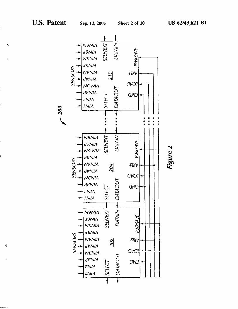
35 first circuit. In other words, a signal is not directly routed to a plurality of circuits. Instead, a signal is received by a first circuit that then controls a similar functionality of a second circuit, possibly dependent on a state of the first circuit. FIG. 2 shows a schematic diagram of a data acquisition
system (200) in accordance with an embodiment of the present invention. The data acquisition system (200) includes a plurality of monolithic integrated circuits (202, 204, 210).
Each monolithic integrated circuits (202, 204, 210) is similarly arranged.
Each monolithic integrated circuits (202, 204, 210) includes a plurality of sensor input signal lines (VIN1, VIN2, VIN3P, VIN3N, VIN4P, VIN4N, VINSP, VINSN,
50 VIN6P, VINQN). The sensor input signal lines (VIN1, VIN2) are single ended sensor input signal lines. The sensor input signal lines (VIN3P, VIN3N, VIN4P, VIN4N, VINSP, VINSN VIN6P, VINQN) are differential sensor input signal
15 described in detail to avoid obscuring the invention.
30
4o
45
FIG. 4 shows a schematic diagram of a control circuit in
FIG. 5 shows a schematic diagram of a two-stage differ-
lines, The input signal lines VIN3P, VIN&, VIN~P,
input signal lines VIN3N, VIN4N, VINSN, and VINQN are I I G g d l l v G LCIIJUI Illpur > ,pa l 'l,,L.Y, L L J p b r r "U,, l l W I L l VI.* "1
dance with an embodiment of the present invention. more sensors. Each single ended Sensor input signal line (VIN1, VIN2)
amplifier circuit in accordance with an embodiment of the 60 and differential sensor input signal lines (VIN3P and present invention. VIN3N, VIN4P and VIN4N, VINSP and VINSN, VIN6P and
FW. 7 shows a schematic diagram of a second differential VIN6N) are amplified by an amplifier circuit and filtered by amplifier circuit with conversion to a single ended output in a filter circuit. Each filter circuit may be an analog, multiple accordance with an embodiment of the present invention. pole filter circuit. In other words, each channel is amplified
amplifier circuit in accordance with an embodiment of the Monolithic integrated circuit (202) receives a SELECT present invention. signal disposed on a daisy chained input control signal line.
accordance with an embodiment of the present invention. 55 and VINQp are positive input signal lines and
,.-+:-l ---l:C-- -:--..:e ... :+l. --:- nn-trnl rn-mnn) in orrnr- ----A:..- - -_-__: _-.. , -:---l I:--" r,.e..-,.t:..~l., Tr,- nnP nr L l I U a l a r l l p l l ~ ' L L L L Y I L w.111 ~ L U L , I " L . U " . ....'---- ', ... -----
FIG. 6 shows a schematic diagram Of a first differential
FIG. 8 shows a schematic diagram of a single ended 65 and filtered.

US 6,943,621 B1 5 6
The SELECT signal may sclect a filtcrcd, amplified sensor Each singlc ended sensor input signal line (VINl, VIN2) signal (or channel) from one of the plurality of scnsor input and diKcrcntial sensor input signal lines (VIN3P and signal lincs to bc output on a DATAOUT output signal linc. VIN3N, VIN4P and VIN4N, VIN5P and VINSN, VIN6P and FuflhCmorC, the SELECT signal may bc daisy chained on VIN6N) arc amplified by an amplifier circuit (302,304,306, the monolithic intcgrated circuit (202) as a SELNEXT signal 5 308, 310, 312). The amplifier circuit (312) receives a GO disposed on a daisy chained output control signal line. The control signal from the control circuit (370). ne SEL daisy chained output control signal line of the monolithic control signal output from the amplifier circuit (312) is integrated circuit (202) may operatively conncct to a daisy as a GO control signal by thC amplifier circuit chaincd input control signal linc of thc monolithic integrated (310), GO control signal and SEL control signal arc circuit (204).
10 daisy chaincd bctween each of the amplifier circuits (302, The SELECT signal may sclect a filtcrcd, amplified 304, 306, 308, 310, 312), sensor signal (or channel) from onc of the plurality of sensor
input signal lincs on thc monolithic intcgratcd circuit (204) 10 be output on a DATAOUT output signal linc of the circuits (302,304,306,308,310,312) and the daisy chaincd monolithic intcgratcd circuit (204). Thc DATAOUT output GO control signal and SEL control signal sclect one channcl signal line of thc monolithic intcgratcd circuit (204) may be l 5 to respond to commands. Accordingly, a selected channcl daisy chaincd to a DATAIN input signal linc of the mono- may adjust gain values for thc amplifier circuits (306, 308, lithic integrated circuit (202). Accordingly, the DATAOUT 310, 312). Also, the selccted channel may output an output output signal linc of the monolithic intcgratcd circuit (202) signal on a DATAOUT output signal Iinc. Furthermorc, thc carries an amplified, filtered sensor signal originated on the control circuits (370) outputs a SELNEXT signal that may monolithic integrated circuit (204). 20 also bc uscd as a SELECT signal received by a control
One of ordinary skill in thc art, having bencfit of this circuit in another, similarly arrangcd data acquisition system disclosure, will undcrstand that a plurality of similarly (300). arranged monolithic integrated circuits may be daisy Gain signals (G2, G5, G20, and GHI) are output from chained so that a daisy chained control signal (c.g., SELECT
lines, and daisy chain an amplified, filtcrcd sensor signal through the plurality of similarly mang@ monolithic inte. grated circuits to a desired output signal linc.
A calibration signal CAL is connected to each of thc signal lincs CMD, LOAD, and PWRSAVE, may conncct to 30 amplifier Circuits (302, 304. 306, 308, 3107 312). ThC each of the plurality of monolithic intcgratcd circuits (202, calibration signal CAL may bc used to allow an offset 204,210). Also, an analog referencc voltagc potential AREF voltagc potcntial on at least onc of the plurality of sensor on an analog control signal linc may connect to each of the input signal lines (VIN1, VIN2, VIN3P, VIN3N, VIN4P, plurality of monolithic integrated circuits (202, 204, 210). VIN4N VINSP, VINSN, VIN6P. VlNQN) to bc calibrated. Accordingly, some control signal lincs may not be daisy 35 Thc olTsct voltagc potcntial may bc calibrated using a chained between the plurality of monolithic intcgratcd cir- sclccted amplifier circuits (302,304,306,308,310, or 312). cuits (202, 204, 210). A calibration for all of the plurality of sensor input signal
One of ordinary skill in the art, having benefit of this h c s (VIN1, VIN2, VIN3P, VIN3N, VIN4P, VIN4N, VINSP, disclosure, will understand that a single monolithic intc- VINSN, VIN6R VIN6N) may Occur by calibrating each of grated circuit (202, 204, or 210) may bc used in a data 40 the amplifier circuits (302,3O4,306,308,310,312) in tum. acquisition systcm. Furthermorc, a largc number of mono- Each amplifier circuits (302,304, 306, 308, 310, 312) lithic integratcd circuit (202,204,210) may be used dcpcnd- outputs an output signal VOUT rcsponsivc to thc scnsor ing on a number of scnsor signal lines desired. Thc mono- input signal lincs (VIN1, VIN2, VIN3P, VIN3N, VIN4P, lithic integrated circuit (202,204, 210) may includc CMOS VINJN, VIN5P, VINSN, VINBP, VINQN). The output signal transistors. 45 VOUT from each of the amplificr circuits (302, 304, 306,
system (300) in accordancc with an embodiment of the (322,324,326,328,330,332). T h C f i k r circuits (322,324, present invcntion. The exemplary data acquisition system 3267 328,330,332) filler the output signal VOUT from each (300) may be disposed on a single monolithic integrated of thc amplifier circuits (302,304, 306,308,310,312). Thc circuit. Also, thc data acquisition system (300) may usc 50 f i h circuits (322, 324, 326. 328, 3307 332) outputs an discrctc componcnts. Furthermore, thc data acquisition sys- output Signal VOUT 10 the sccond of two filtcr circuits (342, tem (300) may bc disposcd on a plurality of monolithic 34,346,348,350, 352). A cutom frcqucncy of the sccond integrated circuits. of two filtcr circuits (342, 344, 346, 348, 350, 352) is T ~ c cxcmplary data acquisition system (300) includes a controkd by the signal SLOW gcncratcd by the control
control circuit (370) that controls various functionalitics 55 circuit (370). A gain of the amplificr circuits (302,304,306, within othcr circuits in the data acquisition system (300). A 308* 310. 312) and/or a cutoff frequency of any of thc filtcr plurality of ScnSor input signal lines (VIN1, VIN2, V[N3P, (322. 324, 326, 328, 330, 332, 342, 3 4 , 346, 348, VIN3N, VIN4P, VIN4N, VINSP, VINSN, VINfjp, VIN6N). 350* 352) may bc controkd by a control mcmoV that may mc scnsorinput signal lines (VIN1, ~ 1 ~ 2 ) arc single cndcd bc hated at anywhere within or cxtcmal 10 thC data SCnSOr input signal lincs. Thc sensor input signal lines 60 acquisition system (300). (VINJP, VIN3N. VIN4P, VIN4N. VINSP, VlN5N VINBP, Thc combincd first of two filtcr circuits (322, 324, 326, VIN6N) arc diffcrcntial sensor input signal lints. Thc sensor 3283330,332) and the sccond of two filtcr circuits (342,344, input signal lincs VIN3P, VIN4P, VINsp, and VlN6P are 346, 348, 350, 352), respcctivcly, providc an analog, mul- positivc scnsor input signal lincs and SCnsor input signal t iPlC Pole filtcr circuit for each of the channels. lincs VINJN, VIN4N, VIN5N. and VIN6N arc ncgalivc 65 In onc or more embodiments of the prcscnt invention, sensor input signal lines, respectively, from onc or more each channel is amplified and filtcred. One channel may be sensors. output at any given time. Each of the second of two filler
SELECT signal rcccivcd tach of the
control circuit (370). The gain signals (G2, G5, G20, and
circuits (306, 308, 310, 312). Amplifier circuits (302, 304)
signal) may sclcct least One Of many input signal 25 CHI) control an amount of gain by the amplifier
havc a fixed unity gain. Other control signal lines, for example, digital control
HG. 3 shows a schematic diagram of an data acquisition 308, 310, 312) is rcceivcd by the first Of two filtcr circuits
US 6,943,621 B1 7
circuits (342, 344, 346, 348, 350, 352) includes a DATAIN input signal line and a DATAOUT output signal line. Depen- dent on the control circuit (370), one of the channels may be selected. For any channel that is not selected, the signal received on the DATAIN input signal line is output on the DATAOUT output signal line. Furthermore, the DATAIN input signal line operatively connected to the filter circuit (342) may be provided by another, similarly arranged data acquisition system (300).
For the channel that is selected, a filtered output signal from the second of two filter circuits (342, 344, 346, 348, 350, or 352) is output on the DATAOUT output signal line. Accordingly, the DATAOUT output signal line from the filter circuit (352) canies the filtered output signal from any selected channel. The DATAOUT output signal may be provided to another, similarly arranged data acquisition system (300).
One of ordinary skill in the art, having benefit of this disclosure, will understand that each of the second of two filter circuits (342, 344, 346, 348, 350, 352) may include a switch circuit (Le., output multiplexing switch). The switch circuit in each of the second of two filter circuits (342,344, 346,348,350,352) may select between the DATAIN input signal line and a local filtered output signal. Aplurality of the second of two filter circuits (342, 344, 346, 348, 350, 352) may be arranged so that one filtered output signal is selected and the other of the second of two filter circuits (342, 344, 346, 348, 350, 352) transport the filtered output signal to a desired output signal line (e.g., DATAOUT output signal line). The switch circuit in each of the second of two filter circuits (342,344,346,348,350,352) may be responsive to a daisy chained control signal line (e.g.. SEL control signal line).
One of ordinary skill in the art, having benefit of this disclosure, will understand that the data acquisition system (300) may be arranged to have a switch circuit (i.e., output multiplexing switch) that selects a filter circuit output and/or an amplifier circuit output.
In one or more embodiments of the present invention, each channel is active. Accordingly, the amplifier circuits (302, 304, 306, 308, 310, 312) are not switched, which reduces noise. Because noise and analog circuit effects are considered, at least one of the amplifier circuits (302, 304, 306, 308, 310, 312) and/or at least one of the filter circuits (322,324,326,328,330,332,342,344,346,348,350,352) may be auto-routed.
In a typical analog circuit design, matching between analog circuit elements is critical for proper operation of the analog circuit. In one or more embodiments of the present invention, bias signals (e.g., BIAS, NBIAS) are transmitted as voltages. Accordingly, current mirrors, and other analog bias circuits, may be distributed across the data acquisition system (300). Furthermore, parts of a current mirror, and other analog bias circuits, may be split and distributed across the data acquisition system (300). Accordingly, it is practical tinar at ieasr one of tine ampiifier circuits (302,3% 3% 3%. 310, 312) and/or at least one of the filter circuits (322, 324, 326, 328, 330, 332, 342,344,346,348, 350,352) may be auto-routed.
The data acquisition system (300) may include CMOS transistors. Other signal lines that are shown, but not described in FIG. 3, will become apparent as other figures are described.
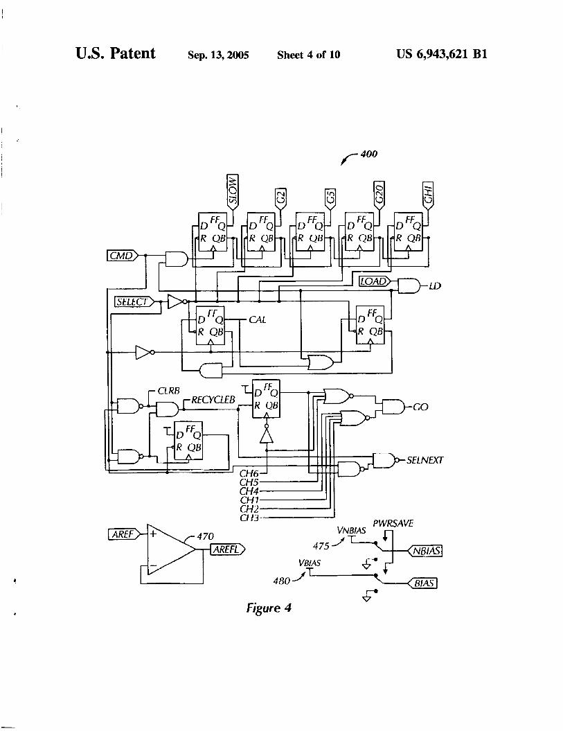
FIG. 4 shows a schematic diagram of a control circuit (400) in accordance with an embodiment of the present invention. The exemplary control circuit (400) may be used
8 as the control circuit (370) shown in FIG. 3. The control circuit (400) receives a LOAD signal, SELECT signal, CMD signal, PWRSAVE signal, and AREF signal. The LOAD signal, SELECT signal, CMD signal, and PWR-
5 SAVE signal are digital signals that may remain at a fixed logic state or user controlled using a number of digital pulses. The AREF signal is an analog reference signal.
The LOAD signal, for example, may be fixed at a logic high state. The SELECT signal and CMD signal may have
10 a number of logical high pulses at user selected times to input commands to the control circuit (400). For example, dependent on a logic circuit arrangement, the following table of input signals may have the listed results.
15
Operation Command
Master Clear Recycle IO Start
20 Select channel N Load
After Channel Select
Number of CMD Read channel
Two SELECT pulses while CMD high CMD pulse while SELECT high N S E L E n pulses from Recycle or Master Clear Transfer command register to selected channel (may be fixed at a logical high)
25 pulses = 1 Number of CMD Read offset voltage potential (calibration)
~~
pulses = 2 Number of CMD pulses = 3+
Gain = 1 , 2, 5 , 10, 20,40, 100, 200, u, u, u, u, 400, u, u, u (u = undefined) (First CMD pulse activates filter (SLOW active), next CMD pulse sets gain = 2 (SLOW inactive), next CMD pulse sets gain = 2 (SLOW active), next CMD pulse sets gain = 5 (SLOW inactive), next CMD pulse sets gain = 5 (SLOW active), etc.)
30
35 In one or more embodiments of the present invention, after the control circuit (400) is cleared, a channel may be selected. Channels are selected dependent on signals carried by a SELECT signal line (shown in FIG. 3) routed to all the amplifier circuits (302, 304, 306, 308,310, 312) and daisy
40 chaining the GO signal and SEL control signal between the amplifier circuits (302,304,306,308,310,312). The initial GO signal is shown in FIG. 4.
If a number of SELECT signals exceeds a number of 45 channels within the data acquisition system (300 shown in
FIG. 3), the SELNEXT signal may select a channel in a next, similarly arranged data acquisition system (300 shown in FIG. 3). The SEL control signal from each channel is received by the control circuit (400) as signals CH1, CH2,
5o CH3, CH4, CH5, and CH6. When the CH6 transitions to an active state, the next SELECT signal causes the SELNEXT signal to become active. The SELNEXT signal acts as the SELECT signal for the next, similarly arranged data acqui- sition system (300 shown in FIG. 3).
In one or more embodiments of the present invention, after the control circuit (400) is cleared and a channel
to the control circuit (400). The CMD signal is used to clock two flip flops, which active a calibration signal CAL on the
60 second pulse. The calibration signal CAL allows an offset voltage potential on at least one of the plurality of sensor input signal lines (VIN1, VIN2, VIN3P, VIN3N, VIN4P, VIN4N, VINSP, VINSN, VINQP, VIN6N shown in FIG. 3) to be calibrated. A third pulse of the CMD signal deactivates
In one or more embodiments of the present invention, the CMD signal may continue to be pulsed after calibration. The
55
selecizd, the CME SigEd may bc i;u!scd :G inpl;: COT"T2EL?dS
65 the calibration signal CAL.

US 6,943,621 B1 9 10
third CMD signal pulse causcs the SLOW signal to become active, which changes a cutor frequency of the sclcctcd filter circuit (342,344,346,348,350, or 352) shown in FIG. 3. The fourth CMD signal pulse causes thc SLOW signal to becomc inactivc and increases a dcfault gain of unity to a 5 gain of two for the amplifier circuits (306, 308, 310, 312) shown in FIG, 3, The fifth CMD signal pulse causes thc
of two for thc arnplificr circuits (306,308,310,312) shown in FIG, 3. Thc sixth CMD signal pulse signal to become inactive and incrcascs gain of two to a gain
in FIG. 3. The above pattern continucs according to the logic shown in FIG. 4. The gain may bc switchcd dependent on a
differential amplifier circuits (550, 560). Each of the differ- cntial amplifier circuits (550,560) may provide a portion of any final gain achicvcd by the differential amplifier circuits (550, 560).
Flip flop (502) maintains a local state for a selection circuitry. The flip flop (502) also Propagates the daisy chained SEL control Signal fmm one amplifier circuit (302,
304, 306, 308, 310, 312). flops (5047 5067 '08, 510) the SLOW l o maintain a local statc for the gain control memory circuitry.
a gain Other
Start command if thc channel is selected and programmed with a
FIG. 6 shows a schematic diagram of a first diffcrcntial amplifier circuit (600) in accordance with an embodiment of
fier circuit (600) may be used as the diEerentia1 amplifier
SLOW signa] to become active again and maintains the gain 304, 306, 308,310, 312) to another amp1ificr circuit (302,
flip 5067 508' 510) may of five for thc circuits (306, 308, 310, 3.2) shown lhan a dcPault unity gain a Master Or Recycle
gain,
uscr command. 15
In One Or mort Of present the present invention, The exemplary first differential ampli- SELECT signal pulses Occur while the CMD
signal is logic high, a CLRB signal is pulsed, which rcscts (550) shown in FIG. 5, all the gain scttings in thc amplifier circuits (306,308,310, 2o first differential amplifier circuit (600) includes a
plurality of switchcs that arc controlled by gain signals (G2, 312). Also, i f the CMD signal PUISCS while the SELECT signal (35, and (320). The gain signals (G2, G5, and G20) may be
is logic high, thc flip flops within the control circuit (400) arc operatively connected to gain signals external of thc first and a RECYCLEB signal is transmitted lo reset hC differential amplifier circuit (600) that represent different
selcct logic within thc amplificr circuits (302,304,306,308, 25 gain values than implied by the labels, The plurality of 310, 312). switches dcterminc which resistors, and conscqucntly which
An analog rcfcrcnce voltage potential AREF on an analog resistor values, arc operatively connected to operational control signal Iinc is buffered in the control circuit (400) by amplifiers (602,604). A gain ofthe first differential amplifier a Unity gain operational amplifier (470) to generate a local circuit (600) is rcsponsive to the resistor values detcrmincd analog rcfcrcncc voltage potential AREFL. The PWRSAVE 3o by thc plurality of switches. A BIAS signal and NBlAS
signal bctwcen a voltage Source (475,4801, rcspcctively, and reference voltagc (e%, a ground voltage potential). SelCc- FIG. 7 shows a schematic diagram of a second differential lively switching to the reference voltage reduces the power amplifier circuit with conversion to a single ended output consumed by circuits operativcly conncctcd to the NBIAS 35 (700) in accordance with an of thc prcscnt signal and the BlAS signal. invention. The exemplary second differential arnplificr cir-
Onc or ordinary skill in thc art will understand that thc cuit with conversion to a single ended output (700) may be control circuit (400) and control signal lines providc one or used as the differential amplifier circuit (560) shown in FIG. many possible arrangements. A control circuit that operates 5. The second differential amplifier circuit with conversion in a different manncr but achieves an equivalent function- 40 to a single ended output (700) includes a plurality of ality should be construed to be within the scope of thc switches that are controlled by gain signals (G2, GS, and present invention. Furthermore, digital signals may be active G20). The gain signals (G2, G5, and G20) may be opcra- as either a logic high or logic low signal. Circuits may be Lively connected to gain signals external of the second designcd that function as above using an oppositc state. differential amplificr circuit with conversion to a singlc Furthermore. diffcrcnt circuitry may be dcsigncd that opcr- 45 ended output (700) that rcprcsent different gain values than ales in a differcnt manner but achieves an equivalent func- implied by the labels. The plurality of switchcs dctcrminc tionality. The different circuitry should be construed to be which resistors, and consequently which resistor values. arc within thc scope of thc prescnt invention, operatively connectcd to operational amplifiers (702,704). A FIG. 5 shows a schematic diagram of a two-stage differ- gain of the second differcntial amplifier circuit with conver-
ential amplificr circuit with gain control memory (500) in 50 sion to a single ended output (700) is responsive to thc accordancc with an embodimcnt of the present invention. resistor values determined by the plurality of switches. The cxcmplary two-stage differential amplifier circuit with The second differential amplifier circuit with conversion gain control mcmory (500) may bc uscd as the amplifier to a single ended output (700) converts a differcntial input to circuit (306, 308,310,312) shown in FIG. 3. A calibration a single ended output VOUT using operational amplifier signal CAL may bc uscd to allow an offsct voltagc potential 5 5 (706). The singlc ended output VOUT is reprcscntative of on at lcast onc of thc plurality of scnsor input signal lincs the output signal VOUT shown in the arnplificr circuits (306, (VIN3P. VINJN, VIN4P. VIN4N. VINSP, VINSN, VIN6P, 308,310,312) shown in FIG. 3 and the differential amplifier VlN6N shown in FIG. 3) to bc calibrated. The calibration circuit (560) shown in FIG. 5. A local analog referencc signal CAL sclccts whcthcr a switch circuit connccts at lcast voltage potential AREFL is operatively connected to an onc of thc plurality of scnsor input signal lincs (VIN3P, 60 input terminal of the operational amplifier (706). The local VIN3N, VIN4P. VIN4N, VIN5P, VINSN. VIN6P, VIN6N analog reference voltage potential AREFL may be used a shown in FIG. 3) or a local analog rcfcrcncc voltagc mcms to adjust an offset voltage potential of the differential potcntial AREFL to thc inputs of a diffcrcntial amplificr amplifier circuit (500) shown in FIG. 5. A BIAS signal and circuit (550). NBlAS signal provide a bias signal to the operational
nects to a second differential amplificr circuit (560). Gain FIG. 8 shows a schematic diagram of a single ended signals (G2, G5. (320, and CHI) arc distributed between the amplifier circuit (800) in accordance with an embodiment of
signal sclcctivcly switches XI NBlAS signal and a BIAS signal provide a bias signal to the operational amplifiers (602, 604).
The difkrcntial amplifier circuit (550) operatively con- 65 amplifiers (702, 704, 706).

US 6,943,621 B1 11 12
the present invention. The exemplary single ended amplifier A calibration signal CAL may be used to allow an offset circuit (800) may be used as the amplifier circuit (302,304) voltage potential on at least one of the plurality of sensor shown in FIG. 3. A calibration signal CAL may be used to input signal lines (VIN1, VIN2, VIN3P, VIN3N, VIN4P, allow an offset voltage Potential on at least one of the VININ, VINSP, VINSN, VINQP, VINCN shown in FIG. 3) plurality of sensor input signal lines (VIN1, VIN2 shown in to be calibrated, FlG. 3) to be calibrated. The calibration signal CAL selects skill in the art, having benefit of this whether a switch circuit connects at least one of the plurality disclosure, will undersland that a channel supports at least of sensor input signal lines (VIN1, V1N2 shown in FIG. 3) one input signal line and the channel may include an or a local analog reference voltage potential AREFL to the input of a single ended amplifier circuit (784). amplifier circuit and/or a filter circuit. The amplifier circuit
10 may be a single ended, multiple ended, or differential The single ended circuit (784) outputs a VOUT signal to a subsequent stage in a channel. For example, the single amplifier circuit. The amplifier circuit may have one or more ended amplifier circuit (800) may operatively connect to a stages and One Or more amp1ifiers. Each may filter circuit (322, 324) shown in FIG. 3. provide a gain, which includes a unity gain or attenuation.
Flip flop (782) maintains a local state for a selection The filter circuit may have one or more poles and one or circuitry. The flip flop (7822) also propagates the daisy 15 more stages. The filter circuit may include passive and/or chained SEL control signal from one circuit (302, active circuit elements. Furthermore, a channel may have
304, 306,308, 310, 312). circuit(s) in an arrangement such that the filter circuit(s) and amplifier circuit(s) may be in any order. In other words, a One or ordinary skill in the art will understand that the single ended amplifier circuit (800) may also include a gain 20 filter circuit may precede an amplifier circuit, and vice versa. Also, filter circuits and amplifier circuits may be inter- control memory circuitry. For example, the single ended spersed between each other and/or grouped together. Also, a amplifier circuit (800) may be arranged to respond to a gain multiplexing switch may bc used to select a filter circuit control memory circuitry similar to that shown in FIG. 5.
Accordingly, a gain of the single ended amplifier circuit output and/or an amplifier circuit output. Further, a multi- 25 plexer may be used to provide a “many-to-one” connection (800) may be adjusted and/or user controlled and selected. between several circuits to a single circuit. FIG. 9 shows a schematic diagram of a filter circuit (900)
One of ordinary skill in the art, having benefit of this in accordance with an embodiment of the present invention. The filter circuit (900) may be used as the filter disclosure, will understand that sensors may sense a vary of circuit (322, 324, 326, 328, 330, 332) shown in HG, 3, The different physical characteristics that include, but arc not filter circuit (900) includes a fixed cutoff frequency filter 30 limited to, temperature, weight, force, acceleration, position,
any physical characteristic (e.g.. a signal carried by a radio amplifier (802). The operational amplifier (802) is opera- tively connected to an NBIAS signal and a BIAS signal. The frequency)‘ BIAS signal and NBIAS signal provide a bias signal to the 35 operational amplifier (802). disclosure, will understand that a control signal that controls
voltage potential on at least one of the plurality of circuits or directly connected to the plurality of circuits. A input signal lines (VIN1, vm2, circuit includes a group of circuit elements on an integrated VIN4N, VINsP, VINSN, VINQP, VIN6N shown in FIG. 3) 4o circuit, an entire integrated circuit, and/or a plurality of
integrated circuits. The circuits may include, but are not to be calibrated. limited to, CMOS transistor(s), bipolar junction FIG. 10 shows a schematic diagram of a filter circuit with transistor(s), a combination of CMOS transistor(s) and bipo- pole frequency control memory and an output multiplexing lar junction transistor(s), gallium based transistors, other
present invention. The exemplary filter circuit with pole 45 circuits, and passive components including frequency control memory and the output multiplexing switch (1OOO) may be used as the filter circuit (342, 344, integrated passive components‘
polc frequency control memory and the output multiplexing more of the following. In one or more embodiments, each switch (1000) includes a filter circuit operatively connected 50 channel is amplified and filtered. Accordingly, delays asso- to a unity gain operational amplifier (902). ne filter circuit ciated with switching shared amplifier circuits and/or filter has a cutoff frequency that may be switched dependent on a circuits is not required. user command. A flip flop maintains a state of the filter In one or more embodiments, because a daisy chained circuit’s cutoff frequency (i,e., pole frequency control control signal line is used, fewer routing lines are required memory). 55 to be routed to a plurality of circuits. Accordingly, a data
???e operational amplifier (9!)2) is operatively connected acquisition system may be smaller. more Cir-
to an NBIAS signal and a BLAS signal. ne BIAS signal iuiis *&h :: fixe:! and NBIAS signal provide a bias signal to the operational size. amplifier (902). The filter circuit (1000) includes a switch In one or more embodiments, because a daisy chained circuit (i.e., output multiplexing switch) that selects between 60 input signal line and output signal line are used, fewer an output signal line of the operational amplifier (902) and routing lines are required to be routed to a plurality of a DATAIN signal line on which to output a signal on a circuits. Accordingly, a data acquisition system may be DATAOUT output signal line. The DATAIN signal line may smaller. Furthermore, more circuits may be used in a data be operatively connected to another filter circuit (342, 344, acquisition system with a fixed size. 346, 348, 350, 352) shown in FIG. 3. Thc switch circuit is 65 In one or more embodiments, because data acquisition dependent on the SEL control signal, which is dependent on system is arranged to have a daisy chained control system a user command. and a daisy chained input signal line and output signal line,
One of
304, 306, 308, 310, 312) to another amplifier circuit (302, one or more circuit(s) One Or more
circuit operatively connected to a unity gain operational radio frequency, specmm~ energy* and signals carried by
an antenna may be a sensor’ One of ordinary skill in the art, having benefit of this
A calibration signal CAL may be used to allow an offset a plurality Of circuits may be daisy between the
VIN3N, vIN4p,
switch ( 1 m ) in accordance with an embodiment of *e Group III-Iv materials, all optic- circuits, electro-optical and
346, 348,350, 352) shown in HG, 3, The filter circuit with Advantages of the present invention may One or
b~ “sed ii; ii diitii acql;isi:i~

US 6,943,621 B1 13 14
multiple similarly arranged monolithic intcgrated circuits may be daisy chained. Accordingly, thc data acquisition system may be expandable to accommodate a desired num- bcr of sensor input signal lines.
In one or more embodiments, an analog, multiple pole 5
filler circuit is used in contrast to a singlc pole filter circuit. Furthermore, at least one analog, multiple pole filter circuit is used per channcl. Also, an amplifier circuit is used per channel. Accordingly, offset voltagc potcntial calibration and gains may controlkd and channel basis.
In one or embodiments, bccausc a non-switching amplifier circuit design is used, noisc is advantageously reduced. A reduced noisc design, along with consideration for analog circuit effects, allows at least one of thc amplifier 15 circuits and/or at least onc of the filter circuits to be auto-routed. Furthermore, in a typical analog circuit design, matching between analog circuit clcments is critical for propcr circuit. In One Or more embodiments of the present invcntion, bias signals (C.P.7 2o BIAS, NBIAS) are transmitted as voltages. Accordingly, current mirrors, and other analog bias circuit, may be distributed across a data acquisition system. Also, parts of analog bias circuits may be split and distributed across the data acquisition systcm. Accordingly, i t is practical that at 25 least a part of the analog circuits may bc auto-routed.
In one or more embodiments, a data acquisition system
CMOS transistor may be rclatively small. Accordingly, the data acquisition system may be relatively small or more 30 circuits may be used in the data acquisition system with a fixed size.
In one or more embodiments, becausc a daisy chained control system is used, a controller docs not need to know 35 a number of channels available on each monolithic inte- grated circuit. If a controller simply knows a total number of channels, a single or plural number of integrated circuits may be used. Each integrated circuit may have a different numbcr of channels. Accordingly, the control system is 4o simplificd. Furthermorc, additional channels may be added with a minimum of added complcxity. Also, channels that are accessed morc often may be located earlier in the daisy chain to reduce thc number of control pulses required to access those channels.
While the invention has been described with respect to a limitcd number of embodiments, those skilled in the art, having benefit of this disclosure, will appreciate that other embodiments can be devised which do not depart from the scope of the invention as disclosed herein. Accordingly, the 5o filter circuits is auto-muted. scope of the invention should be limited only by the attached claims.
3. Thc data acquisition system of claim 1, further com-
an input signal line; a first output signal line; a second output signal line; a first switch circuit; and a second switch circuit,
prising:
at least one of the plurality of circuits opcrativcly connects to a first filtcrcd output signal line,
whcrcin at least onc of the plurality of filter circuits operatively connccts to a sccond filtercd output signal line,
wherein the first switch circuit opcrativcly connects the first output signal line to at least onc sclectcd from the first filtcred output signal line and the input signal line, and
whcrcin the second switch circuit opcrativcly connects the second output signal line to at least one sclcctcd from the second filtered output signal line and thc first output signal line.
data acquisition system of claim 3, further com-
On a per lo
Of the
4, prising:
a third output signal line; and a third switch circuit,
may include CMOS transistors, A manufactured size of a wherein at least one Of the plurality of filtcr Circuits operatively connects to a third filtercd output signal line, and
wherein the third switch circuit operatively connects the third output signal line to at least one sclectcd from the third filtcred output signal line and thc second output signal line.
5. The data acquisition system of claim 4, further com-
a daisy chained control signal line, wherein a state of the first switch circuit, the second switch circuit, and the third switch circuit is dependent on the daisy chained control signal line.
6. The data acquisition system of claim 1, further com-
a plurality of control signal lines, wherein at least one line of the plurality of control signal lines is daisy chained between at least two of the plurality of amplifier circuits.
data acquisition system of claim 1, wherein one of the plurality of amplifier circuits and one of the plurality of
8. The data acquisition system of claim 1, wherein at least one of the plurality of amplifier circuits has a user selectable
9. The data acquisition system of claim 1, wherein the 55 data acquisition system is arranged to allow an ofTsct voltage
potential on at least onc of thc plurality of sensor input Signal lines to be calibrated.
10. The data acquisition system of claim 1, whcrcin thc data acquisition system comprises CMOS transistors.
11. A data acquisition system, comprising: a first integrated circuit, comprising:
a plurality of sensor input signal lines, a daisy chained input control signal linc, a daisy chained output control signal linc, an input signal line, an output signal line, and a control signal line; and
PrisiW
prising:
45
7.
What is claimed is: gain. 1. A data acquisition system, comprising: a plurality of sensor input signal Iincs; a plurality of amplifier circuits, whcrcin at least one ofthe
plurality of amplificr circuits operatively connects to at least onc of thc plurality of sensor input signal lines; and
a plurality of filter circuits, wherein each of the plurality 60 of amplificr circuits opcrativcly connects to a different one of thc plurality of filter circuits, and whercin at least onc of thc plurality of filter circuits is an analog, multiple pole filtcr circuit.
2. The data acquisition system of claim 1, whercin each of 65 the plurality of amplifier circuits operatively connects to at least one of the plurality of filter circuits.
US 6,943,621 B1 15 16
a second integrated circuit, Comprising: a third selecting between the third filtered, amplified sensor signals and a second signal dependent on the second output signal to output a third output signal; and
operatively connecting the third output signal to an inte-
16. The method of acquiring data of claim 15, further
controlling the first selecting, the second selecting, and the third selecting dependent on a user command.
17. The method of acquiring data of claim 16, wherein the controlling is dependent on a number of digital pulses.
comprising:
15 command.
a plurality of sensor input signal lines, a daisy chained input control signal line, a daisy chained output control signal line, an input signal line, 5 grated circuit output signal line. an output signal line, and a control signal line, comprising:
wherein the daisy chained output control signal line ofthe first integrated circuit operatively connects to the daisy chained input control signal line of the second inte- 10
grated circuit,
circuit operatively connects to the input signal line of the first integrated circuit,
wherein the control signal line operatively connects to both the first integrated circuit and the second inte- grated circuit, and
wherein the input signal line of the first integrated circuit is responsive to at least one of the plurality of sensor 7n
wherein the output signal line of the second integrated 18. The method of acquiring data of claim 159
controlling a gain of the amplifying dependent on a user
19. The method of acquiring data of claim 18, wherein the
20. The method of acquiring data of claim 15, further controlling is dependent on a number of digital pulses.
comprising: _ _
input- signal lines of the sccond -integrated circuit dependent on the daisy chained output control signal line of the first integrated circuit.
12. The data acquisition system of claim 11, wherein the first integrated circuit and the second integrated circuit 25 comprise CMOS transistors.
13. The data acquisition system of claim 11, the first integrated circuit and the second integrated circuit, further comprise:
an amplifier circuit, wherein the amplifier circuit opera- tively connects to at least one of the plurality of sensor input signal lines; and
a filter circuit, wherein the filter circuit is an analog, multiple pole filter circuit, and wherein the filter circuit operatively connects to the amplifier circuit.
14. The data acquisition system of claim 13, wherein the amplifier circuit has a user selectable gain, and wherein a gain of the amplifier circuit is dependent on the control signal line.
15. A method of acquiring data, comprising: inputting a plurality of sensor signals; amplifying the plurality of sensor signals to produce a
plurality of amplified sensor signals; filtering the plurality of amplified sensor signals, wherein
the filtering uses a plurality of analog, multiple pole filter circuits, and wherein the filtering produces a first filtered, amplified sensor signal, a second filtered, amplified sensor signal, and a third filtered, amplified sensor signal;
a first selecting betwccn the first filtered, amplified sensor signal and an input signal dispose on an integrated circuit input signal line to output a first output signal;
a second selecting between the second filtered, amplified sensor signal and a first signal dependent on the first 0i;:pu; sigii.: to output a sccond output signal;
30
35
40
45
calibrating an offset voltage potential of at least one of the plurality of sensor signals dependent on a user com- mand.
21. A data acquisition system, comprising: means for inputting a plurality of sensor signals; means for amplifying the plurality of sensor signals to
produce a plurality of amplified sensor signals; means for filtering the plurality of amplified sensor sig-
nals to produce a plurality of filtered, amplified sensor signals;
means for selecting one of the plurality of filtered, ampli- fied sensor signals from a first integrated circuit to produce a selected filtered, amplified sensor signal;
means for daisy chaining the selected filtered, amplified sensor signal to a second integrated circuit; and
means for outputting the selected filtered, amplified sen- sor signal from the second integrated circuit.
22. A data acquisition systcm, comprising: a first integrated circuit, comprising:
means for inputting a sensor signal for at least three channels; and
a plurality of means for filtering at least three channels, each of the at least three channels corresponding with a different one of the plurality of means for filtering, and wherein each of the plurality of means for filtering comprises one or more poles.
23. The data acquisition system of claim 22, further comprising:
means for amplifying each of the at least three channels. 24. The data acquisition system of claim 22, further
a second integrated circuit, wherein the second integrated circuit is dependent on a daisy chained control signal line output by the first integrated circuit.
50
comprising:
55 * * * * *