
ubm_edn_201207
64
DIGIKEY.COM/NEW NEW PRODUCTS ADDED DAILY Dissecting the Intel 710 Enterprise SSD Pg 22 EDN.comment Pg 10 Isolation has come a long way, baby! Pg 20 Design Ideas Pg 46 Supply Chain Pg 52 Tales from the Cube Pg 58 JULY 2012 www.edn.com Issue 13 IMAGE SENSORS EVOLVE TO ADDRESS EMERGING EMBEDDED VISION NEEDS EMERGING EMBEDDED- VISION NEEDS Page 32 Advanced power switches boost microhybrid emissions gains Page 27 Applying the interrupt features of MEMS accelerometers Page 42
Transcript of ubm_edn_201207

DIGIKEY.COM/NEW
NEWPRODUCTS
ADDED DAILY
012412_NPAD_EDN_US_snipe.indd 1 1/24/12 1:52 PM
Dissecting the Intel 710 Enterprise SSD Pg 22
eDn.comment Pg 10
Isolation has come a long way, baby! Pg 20
Design ideas Pg 46
supply chain Pg 52
tales from the cube Pg 58
JULY 2012 www.edn.com
Issue 13
image sensors evolve to aDDress
EmErging EmbEddEd vision nEEdsEmErging EmbEddEd- vision nEEds Page 32
advanced power switches boost
microhybrid emissions gains
Page 27
applying the interrupt
features of memsaccelerometers
Page 42


YOUR IDEAS. OUR LOW COST, LOW POWER SOLUTIONS. IT’S GO TIME. At Lattice, we’re helping our customers create the world’s most
innovative products. Our FPGA and programmable power management solutions
are low cost and low power, so you can build the product you need within the time
and budget you want. We’re 100% committed to getting your ideas off the ground
quickly, easily and affordably. Because after all, your ideas inspired our products
in the first place. So keep innovating. We’re ready.
©2012 Lattice Semiconductor Corporation. All rights reserved. Lattice Semiconductor Corporation, L (& design), Lattice (& design) and speci� c product designations are either registered trademarks or trademarks of Lattice Semiconductor Corporation or its subsidiaries, in the United States and/or other countries. Other marks are used for identi� cation purposes only, and may be trademarks of other parties.
TM
Scan this to learn more about our low cost, low power FPGA solutions.
latticesemi.com/go

WWW.COILCRAFT.COM
®
The path of least resistance is through our new high efficiency XAL/ XFL inductors
Compared to competitive parts, current zips right through our new XAL/XFL inductors.
Their DC resistance is signifi-cantly lower than other inductors of the same size. So your batteries last longer and your power supply runs cooler.
They easily handle large peak current, and their soft saturation
characteristics often let you use a smaller size part without fear of overloading during transients.Built from a uniquely formulated material, XAL/XFL parts do not have the same thermal aging prob-lems as some competitive parts.
See all the advantages of these new high efficiency inductors.Visit coilcraft.com/xal.
Electrons prefer Coilcraft
Competitors’ 4.7uH inductors have much higher DCR per mm3
than Coilcraft’s XAL5030.
38% higher DCR
126% higher DCR
48% higher DCR

contents
Cover image: thinkstoCk
image sensors evolve to address emerging embedded-vision needs
32As technology progresses from elementary image capture to more robust image analy-sis, interpretation, and response, semicon-
ductor suppliers and their optics partners are respond-ing with improved image-sensor subsystems.
by Brian Dipert, Embedded Vision Alliance, and Eric Gregori and Shehrzad Qureshi, BDTI
July 2012
D e s i g n i D e a s46 Simple automatic-shutoff circuit uses few components
48 Inverting level-shift circuit has negative potential
49 Single hex-inverter IC makes four test gadgets
▶ Submit your own Design Idea to [email protected].
EDN120510DI5293 Fig 1.eps DIANE
S D
Q1SI4435
R110M
R21k
C110 μF
D19.1V
G+
VOUT
ON
VBATTERY=9V TO 24V
JuLY 2012 | EDN 5[ www.edn.com ]
applying the interrupt features of mems accelerometers
42Understand how to implement reliable and robust interrupt-based applications using MEMS-based
accelerometers.by Jay Esfandyari, Gang Xu, and Paolo Bendiscioli,
STMicroelectronics
advanced power switches boost microhybrid emissions gains
27Packaging and circuit integration deliver
improved performance for start-stop automotive applications.
by Masashi Sekine and Jifeng Qin,
International Rectifier Corp

With local support all over the world,we’re fl uent in technology.
Mouser and Mouser Electronics are registered trademarks of Mouser Electronics, Inc.
mouser.com | The Newest Products for Your Newest Designs®
mouser.comDistributing semiconductors and electroniccomponents for design engineers.
Authorized Distributor
Texas, California, New Jersey USA
Upplands-Väsby SWEDEN
Brive-La-Gaillarde FRANCE
Hong Kong, Shanghai CHINA
Jalisco MEXICO
Brno CZECH REPUBLIC
Eindhoven THE NETHERLANDS
Bangkok THAILAND
Buckinghamshire UNITED KINGDOM
Raanana ISRAEL
Munich GERMANY
SINGAPORE
Barcelona SPAIN
Bengaluru INDIA
Assago-MI ITALY
Taipei TAIWAN
Mouser delivers the components you need, on-time. And with local Technical Support and Customer Service Experts in 19 locations around the world, you’ll fi nd the newest components to launch your new design seamlessly.

EDN® (ISSN# 0012-7515) is published semimonthly (January–June) and monthly (July–December) by UBM Electronics, 600 Community Drive, Manhasset, NY 11030-3825. Periodicals postage paid at Manhasset, NY, and at additional mailing offices. SUBSCRIPTIONS—Free to qualified subscribers as defined on the subscription card. Rates for nonqualified subscriptions, including all issues: US, $150 one year; $250 two years; $300 three years. Except for special issues where price changes are indicated, single copies are available for $10 US and $15 foreign. For telephone inquiries regarding subscriptions, call 847-559-7597. E-mail: [email protected]. CHANGE OF ADDRESS—Notices should be sent promptly to EDN, PO Box 3609, Northbrook, IL 60065-3257. Please provide old mailing label as well as new address. Allow two months for change. NOTICE—Every precaution is taken to ensure accuracy of content; however, the publishers cannot accept responsibility for the correctness of the information supplied or advertised or for any opinion expressed herein. POSTMASTER—Send address changes to EDN, PO Box 3609, Northbrook, IL 60065-3257. CANADA POST: Publications Mail Agreement 40612608. Return undeliverable Canadian addresses to APC, PO Box 503, RPO West BVR CRE, Rich Hill. ON L4B 4R6. Copyright 2012 by UBM. All rights reserved. Reproduction in whole or part without written permission is prohibited. Volume 57, Number 13 (Printed in USA).
contents
departments & Columns
July 2012
54
pulse 12 Scope enhancements simplify
serial-bus debugging
14 Multicore evaluation modules jump-start designs on TMS320C665x KeyStone-based DSPs
14 Microcontrollers target budget applications
16 GaN-on-GaN breakthrough LED boosts MR16 performance
16 Hibernate capability aids power management
19 PWM controllers enable smaller, greener power adapters up to 40W
Dilbert 14
U L T R A M I N I A T U R ESURFACE MOUNTDC-DC ConverterTransformers &Power Inductors
or send directfor FREE PICO Catalog
Call toll free 800-431-1064in NY call 914-738-1400
Fax 914-738-8225PICO Electronics,Inc.143 Sparks Ave. Pelham, N.Y. 10803-18889
E Mail: [email protected]
Transformers can be used forself-saturating or linear switching applications. The Inductors are ideal fornoise, spike and power filtering applications in Power Supplies, DC-DCConverters and Switching Regulators.
See full Catalog immediately
www.picoelectronics.com
Delivery-Stock to one weekfor sample quantities
• Transformers have input voltages of 5V, 12V, 24V, and48V. Output voltages to 500V
• All units can be supplied withhigher or lower secondaryvoltages at the same powerlevels
• Transformers can be used forself-saturating or linearswitching applications
• MIL-PRF-27(+1300C) (Class V 1550C available)
• Inductors have split windings• Schematics and part list
provided with transformers
[ www.edn.com ]
58
8 EDN online: Join the conversation; Content; Engineering Community
10 EDN.comment: Lasting impact of good engineering
20 Baker’s Best: Isolation has come a long way, baby!
22 Teardown: Dissecting the Intel 710 Enterprise SSD
24 Mechatronics in Design: Engineering education upheaval
52 Supply Chain: Questions linger on anti-counterfeit rules; Medical to fall under ROHS scope in 2012; Contract manufacturers capitalize on shift to ultrabooks
54 Product Roundup: Components and Packaging
58 Tales from the Cube: This one really takes the cake— and the schematics

online
EnginEEring communityOpportunities to get involved and show your smarts
Join thE convErsationComments, thoughts, and opinions shared by EDN’s community
contEntCan’t-miss content on EDN.com
What’s your favorite joke about engineers?Who says engineers don’t have a sense of humor? In late June, EDN asked its audience for their favorite joke about engineers or engineering. Nearly 100 jokes and comments have been posted so far, each one providing a good laugh. Check them out, and share your own, at www.edn.com/4375942.
FundamEntals oF usB audioTake a look at the USB Audio standard for digital audio and how it works, what to watch out for, and how to use USB Audio for high-fidelity multichannel input and output.
www.edn.com/4376143
In response to “A virtual analog computer for your desktop,” a technical article by Arthur Glazar at www.edn.com/4376400, antolin.agatep_#3 comments:“The point is not about tools, but in the methodologies that are being presented; that is, analog computers were used in solving for ‘analytical’ solutions to differential equations, which required the ‘programmer’ to understand the phenomena in differential or Laplace transform representation. Over many years ... the analog computer approach has fallen into disuse. But its foundations are solid and do rival the digital computer approach.
“Think of operational amplifiers when you think of analog computers. That’s one of their most popular uses. But I have to say, as I’ve also studied analog circuits and design, that this methodology is far from dead.”
In response to “Hearing aids hacked,” posted in the Serious Fun blog at www.edn.com/4376762, AlisonKeen comments:“I think there is merit in what these hackers are talking about. As someone who’s worn hearing aids for a
long time, it is frustrating to talk an audiologist through endless small adjustments that could be done at home ... [via] appropriately set-up software with appropriate hard-code limits.
“To put it into perspective, imagine if you could hook your glasses up to the computer and adjust the focus using some software. The excitement of being able to tinker and make the world clearer is a good incentive for something like this.
“Connecting in to your hearing aids is a good thing. ... If you have to wear the things, why not get the most out of them?”
EDN invites all of its readers to constructively and creatively comment on our content. You’ll find the opportunity to do so at the bottom of each article and blog post.
8 Edn | JuLY 2012 [ www.edn.com ]
disclEss consolE gaming: thE timEs thEy arE a-changin’With the trend toward cloud-based processing and/or downloadable delivery and away from physical media for gaming already in play, recent moves by Sony have one engineer curious about its PlayStation design strategy.
www.edn.com/4375555

brand directorPatrick Mannion, 1-631-543-0445;
executive editor Rich Pell, Consumer
1-516-474-9568 [email protected]
Managing editorAmy Norcross
Contributed technical articles1-781-734-8970;
Managing editor, onlineSuzanne Deffree
Electronic Business, Distribution1-631-266-3433;
Senior technical editorMargery Conner
Design Ideas, Power Sources, Components, Green Engineering
1-805-461-8242; [email protected]
Senior technical editorSteve Taranovich
Analog, Systems Design1-631-413-1834;
deSign ideaS contributing editor
Glen Chenier, [email protected]
chief copy editorDiana Scheben, 1-631-983-7693;
aSSociate editorJessica MacNeil, 1-212-600-3243;
coluMniStSHoward Johnson, PhD, Signal Consulting
Bonnie Baker, Texas InstrumentsPallab Chatterjee, SiliconMap
Kevin C Craig, PhD, Marquette University
contributing technical editorSDan Strassberg [email protected]
Brian Bailey [email protected] Cravotta,
vice preSident/deSign directorGene Fedele
creative directorDavid Nicastro
art directorGiulia Fini-Gulotta
productionAdeline Cannone, Production Manager
Laura Alvino, Production ArtistYoshihide Hohokabe, Production Artist
Diane Malone, Production Artist
EDN EuropEGraham Prophet, Editor
Reed [email protected]
EDN AsiAHuang Hua
Operations General [email protected]
Grace WuAssociate Publisher
[email protected] Nanda
Executive [email protected]
EDN ChiNAHuang Hua, Operations General Manager
[email protected] Wu, Associate Publisher
[email protected] Lu, Executive [email protected]
EDN JApANMasaya Ishida, Publisher
[email protected] Nishisaka, Editor
ubM electronicS ManageMent teaM
Paul Miller, Chief Executive Officer, UBM Technology
Kathy Astromoff, Chief Executive Officer, UBM ElectronicsBrent Pearson, Chief Information Officer
David Blaza, Senior Vice PresidentKaren Field, Senior Vice President, ContentJean-Marie Enjuto, Vice President, Finance
Barbara Couchois, Vice President, Partner Services and Operations
Felicia Hamerman, Vice President, Marketing
Amandeep Sandhu, Director of Audience Engagement
and AnalyticsFor a complete list of editorial contacts, see http://ubmelectronics.com/editorial-contacts
EMULATIONTECHNOLOGY, INC
www.emulation.com1-800-232-7837
Fully automated or manually operated solutions to test any lead pitch & IC package
Quick TurnLow NRE
Custom Test Fixtures
Significantly reduce your socket & labor costs with these multiple
IC test and burn-in solutions.
Multi-Cavity Sockets
QuickOn/Off Lid
Easy Knobconfiguration
Easy Screw - Lid removed to show detail.
Lead pitches as low as 0.4mm, up to 125,000 insertions.Compression, SMT, &Thru-Hole PCB Mounting
[ www.edn.com ] JULY 2012 | edn 9

BY patrick mannion, Brand director
e d n . c o m m e n t
10 EDN | July 2012 [ www.edn.com ]
That book became a source of both comfort and humor at the scene. It was all my son wanted, and whenever someone tried to take it from him to make him lie down or examine him, he wouldn’t let it go. In the end, he had to surrender it; but in the ambulance he reached up with both hands to take it from the officer who was handing it back to him, and he clutched it to his chest like a priest cradling the Gospels. I’ll never shake that image.
They say you can tell a lot by what a person holds dear. So what does it say about me that, even as I counted my blessings, I felt a pang of grief when we arrived home later that evening and I saw the chasm where my car used to be?
I’m generally not too attached to things, but everyone knows I liked that car. It was a 2002 Maxima SE that I’d bought new with a view toward keeping it until its last gasp. I chose it because it had a good engine. Nissan had been hell-bent on making a name for itself
in quality, and ’02 was the last year of that model, so all the bugs had long been worked out.
Ten years and 124,000 miles later, not a single part on that car had failed. Every button was intact; every moving part worked on cue. There had been no wiring problems, no engine trouble, and no sensor issues. I knew that every time I turned the ignition, the engine would start. The Nissan was reliable, trustworthy, and well engineered. It was the perfect car, serving me well even unto its demise.
Eyewitnesses to the accident said I was “lucky” to have been able to slow down the car before impact; I credit the car’s braking and good tires. The crash nearly flipped the SUV, but the Nissan’s front took the hit as designed: The airbags deployed, and the crumple zone sacrificed itself.
Meanwhile, we have a fridge— one of those Kenmore stainless-steel behemoths—that we bought new about
five years ago. Every year, we have to call Sears to fix the same water line. We know the repair guy by name.
My colleague Rich Nass recently complained about his own fridge heater breaking. “Who puts a heater in a freez-er?” he exclaimed. It’s just one more thing to fail.
I’m happy we came away relatively unscathed. I’m going to miss my car, though—not just because it was my car, but because it was one of the best examples of solid engineering I’ve had the pleasure to own.
Hats off to Nissan and to the engi-neers and designers who made that car. Thank you for keeping my son and me intact.EDN
Contact me at [email protected].
Lasting impact of good engineering
I had a nasty accident earlier this month that totaled my car but spared me and my passenger: my 11-year-old son, who was in the rear seat reading a book when we crashed. Everyone’s OK, and the insurance companies will do their necessaries, but how do you mourn a great piece of engineering and thank the people behind it?
The crash was a split-second event. I had been driving along doing 45 to 50 mph when, out of nowhere, a red SUV appeared in front of me, its driver attempting a U-turn to go in my direction. I had nowhere to go; both lanes were blocked. Stopping was the only option. Screech, bang, smoke, fumes, fear, curb, witnesses, police, ambulance, neck braces, stretchers, and suddenly my son and I were lying side by side, blinkered and staring at the ceiling of an ambulance. I tried to reach my wife on a cell phone that, predictably, didn’t work when I most needed it. My son clenched the Harry Potter book he’d been reading for the third time.
Eyewitnesses to the accident said I was “lucky” to have been able to slow down the car before impact; I credit the car’s braking and good tires.
JoiN ThE coNvErsaTioNAny recommendations for a solid, utility car with a bit of oomph? Should I buy a used car or a new one? To comment, go to www.edn.com/4389916.

Features• +3.6V to +16V Operating Input (+20V OV Protection)• Fast-Charging, Flexible 4A Switch-Mode Architecture
•TurboCharge™* current-multiplier cuts charge time by 30%-60%•TurboCharge+™* auto-float voltage control (AFVC) further reduces charge time by compensating for internal battery impedances•CurrentPath™ with dual outputs for system/battery (SMB349) supports instant-on with dead/missing battery•FlexCharge/FlexCharge+™* auto power source detection (APSD/AIVD) per USB2.0/3.0/BC1.2 to detect USB or AC/DC source +5V to +16V•OptiCharge™* auto input current limit (AICL) detects and adapts to source current limit to maximize available power
• I2C Programmable Parameters and Functions with NV Configuration• SafeCharge™ safety features support JEITA/IEEE1725
• Battery and IC over-voltage/current/temperature protection• Trickle charge for deeply-discharged cells• Safety timers and fault monitors/reporting
• Tiny 3.2 x 3.0 CSP and 52mm2/1.2mm z-height solution size
* Patent granted or pending
Finally! Charge Big Batteries Fast With4A Chip-Scale Li-Ion Charger ICs
Flexible USB/AC Input from +3.6V to +16V, Tiny Solution Size, I2C Programmable Parameters and Built-In Safety – Ideal for Tablets and Smartphones
Industry’s Highest System Efficiency
Applications• Tablets• Smartphones• E-Readers• UltraBooks• Battery “JuicePacks”• Portable Gaming• Portable Digital Video
All chargers have Battery Thermal Protection & JEITA Support, IC Thermal Protection, Auto Input Current Limit, Safety or Watchdog Timers, Programmable Charging Parameters, I2C Interface, USB On-The-Go, TurboCharge™ Mode*
Handheld Device
USB2.0/3.0500mA/900mA
4.35V-5.5V
AC/DC Chargerup to 3500mA
4.5V-16V (20V OVP)
I2C (optional)
Syst
em
SMB349Li- Ion
Charging Currentup to 4A
USB
System Outputup to 4A
GN
DV
B US
D-
D+
ID
USB-OTG/HDMI/MHL
5.0V @ 900mAOTG/LBR/HDMI/MHL
~1200 mA
USB Input100/500 /700-3500 mA
"Ideal Diode " Current
Total Sys. Output>4A
SMB349 SMB359 SMB347 SMB137C SMB346 SMB136CInput Voltage Range (V)* 4.35 to 16 (20) 4.35 to 16 (20) 4.35 to 6.2 (20) 4.35 to 6.0 (18) 4.35 to 6.2 (20) 4.35 to 6.0 (18)# of Inputs/Outputs 1/2 1/1 2/2 2/2 2/2 1/2Maximum Charge Current (mA) 4000 4000 2500 1500 1250 1500Maximum Input Current (mA) 3500 3500 2500 1500 2500 1500CurrentPath™ Control √ √ √ √ √Charge Current Voltage Output √ √ √ √Low-Battery Recovery Mode √ √Automatic Power Source Detection ** rev 1.2 rev 1.2 rev 1.1/1.2 rev 1.2 rev 1.1/1.2 rev 1.2
Package 3.2x3.0 CSP-49 5x5 QFN-40
3.2x3.0 CSP-49 5x5 QFN-40 3.0x2.5 CSP-30 3.0x2.5 CSP-30 3.0x2.5 CSP-30 3.0x2.5 CSP-30
Solution Size (mm2) 52 52 32 38 32 35
For more information see:www.summitmicro.com/SMB349

As serial-bus standards have become faster and more complex, debug-ging has become a productivity
issue. Firmware and software updates for several Tektronix digital and mixed-signal oscilloscope families reduce both serial-bus-test complexity and debug time, addressing such standards as PCIe, CAN/LIN, MIL-STD-1553B, and Media Oriented System Transport.
As signal complexity rises—for example, as multilane serial buses become common-place—capturing unique events with an oscil-loscope requires increasingly flexible trigger systems. Tektronix Visual Trigger lets you use a mouse or touchscreen to create highly customizable shapes that closely match the waveform of interest. A “mark all trigger events” feature enables search and capture of an acquisition’s complex behaviors. For greater analysis depth, a custom interface to Matlab data-analysis software provides advanced plotting and filter capabilities. You can install and run Matlab on the scopes, thereby eliminating the need to transmit raw
data to a separate computer for analysis.Concern about crosstalk is rising along
with bus speeds. The software helps Tek-tronix-oscilloscope users identify crosstalk in their designs without resorting to bit-error-rate testing. An algorithm in the DPOjet jitter- and eye-diagram-analysis tool correctly identifies crosstalk-induced jitter as bounded uncor-related jitter; thus you can use real-time oscil-loscopes to measure total jitter and separate crosstalk or intersignal interference from other forms of jitter. Using Microsoft Visual Studio, you can customize DPOjet measurements.
The new version of DPOjet is available now. Firmware updates for DPO (digital-phosphor oscilloscope)/MSO (mixed-signal oscillo-scope) 5000 series, DPO7000C, and DPO/DSA (digital signal analyzer)/MSO70000C/D series oscilloscopes are available free at the Tektronix Web site. Before they can accept the updated firmware, however, many older instruments require Windows 7 installation, for which you must return the instrument to Tektronix. In the United States, the mini-mum charge for that is $692; the exact cost depends on what hardware must be replaced.
—by Dan Strassberg▷Tektronix Inc,www.tektronix.com.
Scope enhancements simplify serial-bus debugging
talkback
000
109
8
7 6 5
43
2
1
pulseINNOVatIONS & INNOVatORS
[ www.edn.com ]
“The optimist says the glass is half full, and the pessimist says the glass is half empty. The engineer looks at them both and says, ‘The glass is twice as big as it needs to be.’” —commenter sparky_, in response to a blog post asking readers to share their favorite engineering joke, at www.edn.com/4375942. add your own joke.
You can now upgrade scopes in Tektronix’s 5000, 7000, and 70000 series with firmware that greatly improves their serial-bus debugging capabilities. For owners of newer instruments—those that are already running Windows 7—the upgrade is free, requiring only a download and installation.
12 EDN | July 2012

>> Find out how LabVIEW can make you better at ni.com/labview/better 800 453 6202
©2010 National Instruments. All rights reserved. LabVIEW, National Instruments, NI, and ni.com are trademarks of National Instruments. Other product and company names listed are trademarks or trade names of their respective companies. 2811
NI LabVIEW
NamePeter Simonsen
Job TitleDesign Engineer,Embedded Software
Area of ExpertiseRenewable Energy
LabVIEW Helped MePerform real-worldsimulations with total control of the application
Latest ProjectDevelop a test architecturefor verifi cation of wind turbine control systems
SIMULATELabVIEW makes me better because I can
real-world systems
Multicore evaluation modules jump-start designs on TMS320C665x KeyStone-based DSPs
The 32-bit STM32 F0 microcontrollers from STMicroelectronics use
an ARM Cortex-M0 processor architecture, which lets devel-opers break the price and per-formance limitations of older, 8- and 16-bit devices.
Built-in RAM-parity check-ing improves real-time perform-ance and helps achieve Class B safety-standards compat-ibility in home appliances. An
integrated clock-security sys-tem enhances reliability, and advanced timing helps over-come common motor-control design challenges. The MCU integrates hardware touch-sensing control, a 12-bit ADC with 1M-sample/sec conver-sion, a 12-bit DAC, and two tightly coupled programma-ble analog comparators. A consumer-electronics control module allows connections to
home multimedia devices using industry-standard protocols.
The MCU has a 1 5.3-μA stop mode and a 2.8-μA standby mode with the real-time clock running, extending battery life. Other features include an SPI with support for a programma-ble date frame as large as 16 bits and a baud rate as high as 18 Mbps, and an I2C port sup-porting communication speeds up to 1 Mbps.
The STM32 F0 offers embed-ded-memory densities of 16 to 64 kbytes of flash and 4 to 8 kbytes of SRAM, along with UFQFPN32, LQFP48, and LQFP64 package options. Another 20-pin version in 16-kbyte flash configuration and extension to 128-kbyte flash in a 100-pin package will soon become available. Pro-grammable analog- and digital-noise filtering ensures robust communications, and a 6-Mbps USART supports multiple clock-input options.
A developer kit, including a prototype board, plugs directly into a PC’s USB port; demon-stration code and sample firm-ware support the kit. The kit sells for $7.99; the STM32 F0 sells for 95 cents (1000).
—by Fran Granville▷STMicroelectronics,www.st.com.
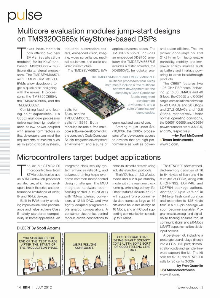
T exas Instruments is now offering two new E V M s ( e v a l u a t i o n
modules) for its KeyStone-based TMS320C665x mul-ticore digital signal proces-sors. The TMDSEVM6657L a n d T M D S E V M 6 6 5 7 L E EVMs allow developers to get a quick start designing with the newest TI proces-sors: the TMS320C6654, the TMS320C6655, and the TMS320C6657.
Combining fixed- and float-ing-point capabil it ies, TI’s C665x multicore processors deliver real-time high perform-ance at low power coupled with smaller form factors so that developers can meet the requirements of markets such as mission-critical systems,
industrial automation, tes-ters, embedded vision, imag-ing, video surveillance, medi-cal equipment, and audio and video infrastructure.
The TMDSEVM6657L EVM
sells for $349, and the TMDSEVM6657LE sells for $549. Both modules include a free multi-core software development kit, the company’s Code Composer Studio integrated development environment, and a suite of
application/demo codes. The TMDSEVM6657L includes an embedded XDS100 emu-lator; the TMDSEVM6657LE includes a faster emulator, the XDS560V2, for quicker pro-
gram load and ease of use.Starting at just under $30
(10,000), the C665x proces-sors offer developers access to devices that are high-per-formance as well as power-
and space-efficient. The low power consumpt ion and 21×21-mm form factor enable portability, mobility, and low-power energy sources such as battery and interface pow-ering to drive breakthrough products.
The C6657 features two 1.25-GHz DSP cores, deliver-ing up to 80 GMACs and 40 Gflops; the C6655 and C6654 single-core solutions deliver up to 40 GMACs and 20 Gflops and 27.2 GMACs and 13.6 Gflops, respectively. Under normal operating conditions, the C6657, C6655, and C6654 power numbers are at 3.5, 2.5, and 2W, respectively.
—by Toni McConnel▷Texas Instruments,www.ti.com.
14 EDN | July 2012 [ www.edn.com ]
pulse
The TMDSEVM6657L and TMDSEVM6657LE multicore processors from Texas
Instruments include a free multicore software development kit, the
company’s Code Composer Studio integrated
development environment, and a suite of application/
demo codes.
DILBERT By Scott Adams
Microcontrollers target budget applications

Strange stories from the call logs of Analog Devices
To Learn More About Multiple Op Amps
http://dn.hotims.com/41007-100
A: That’s a great question. Actually, there’s quite a bit to it, from the perspectives of both the user and the IC designer. Multiple op amps (duals, triples, quads, and even the occasional octal) are very popular with customers who use many op amps in their circuits, and for good reason. Multiple op amps offer the advantages of less board area, reduced cost, and better matching. As for electrical performance, this cuts both ways, and we’ll talk about it in a minute.
In many cases, multiple op amps are a very close approximation to the single amplifier. As you can imagine, there must be some redundancy the IC designer can take advantage of with two “duplicate” amplifiers, right? Yes, you’re right; one example is the op amp’s bias circuitry. Instead of duplicating the bias circuit for each op amp, it is often modified to accommodate all amplifiers, reducing complexity, die area, and cost. Reduced die area has a direct impact on the size and cost of the packaged op amps; it also lowers board cost (smaller board), assembly cost (one insertion), and inventory cost (one part vs. many). The amplifiers share a common piece of silicon, so they track extremely well, providing another advantage.
There are a few things to watch out for, however. Multiple op amps dissipate more
power per package. Since the supply current is multiplied by the number of op amps, the power dissipation will increase; this can result in higher junction tempera-tures. As alluded to, multiples present challenges to the silicon designer as well. One of the issues with multiples is the layout. Compromises must be made, which can result in degradation in some electrical performance. Optimized for flow, size, and performance, the die layout can affect parameters such as offset voltage and drift. Also, due to tighter quarters, crosstalk can become an issue, especially at high frequencies. A few of ADI’s high-speed amplifiers and differential amplifiers are offered with two separate die in a single package, however, providing excellent crosstalk performance and additional design freedom.
In summary, multiple op amps are a great choice when a circuit calls for several op amps, and for good reason: lower costs, smaller PCB area, easier inventory manage-ment, and better electrical performance.
Dual Op Amps and Double Agents: They may not always appear to be who they say they are…
Q: Are dual op amps just duplicates of the single version of the op amp? Do they offer the same performance?
SPONSORED BY
Have a question
involving a perplex-
ing or unusual analog
problem? Submit
your question to:
www.analog.com/
askjohn
For Analog Devices’ Technical Support, Call 800-AnalogD
R A Q ’ sS p e c i a l a d v e r t i S i n g S e c t i o n
Contributing Writer
John Ardizzoni is a
Technical Product
Manager at Analog
Devices in the High
Speed Linear group.
John joined Analog
Devices in 2002, he
received his BSEE
from Merrimack Col-
lege in N. Andover, MA
and has over 30 years
experience in the
electronics industry.
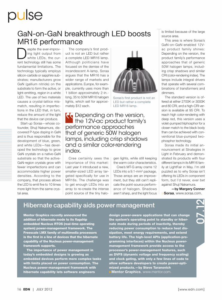
Despite the ever-improv-ing light output from white LEDs, the cur-
rent technology still has some fundamental limitations. The technology typically employs silicon-carbide or sapphire sub-strates; manufacturers grow GaN (gallium nitride) on the substrate to form the active, or light-emitting, region in a white LED. The use of two materials causes a crystal-lattice mis-match, resulting in imperfec-tions in the LED that, in turn, reduce the amount of the light that the device can produce.
Start-up Soraa—whose co-founder, Shuji Nakamura, dis-covered P-type doping in GaN and is thus responsible for the development of blue, green, and white LEDs—has devel-oped the technology to grow GaN crystals on a native-GaN substrate so that the active-GaN-region crystals grow with fewer imperfections and can accommodate higher power densities. According to the company, that process allows the LED to emit five to 10 times more light from the same crys-tal area.
The company’s first prod-uct is not an LED but rather a complete LED MR16 lamp. Although pol i t ic ians have focused on the demise of the incandescent A-lamp, Soraa argues that the MR16 has a wider range of markets and applications. Europe, for exam-ple, currently uses more than 1 billion approximately 2-in.-long, 35 to 50W MR16 halogen lights, which sell for approxi-mately $12 each.
Cree certain ly sees the importance of this market: Last year it introduced a new, smaller-sized LED array tar-geted specifically for use in MR16s. The challenge was to get enough LEDs into an array to re-create the intense point source of the tiny halo-
gen lights, while still keeping the warm color characteristics.
Cree’s MT-G array crams 12 LEDs into a 9.1-mm2 package. Those arrays are an improve-ment, but they still can’t repli-cate the point-source perform-ance of halogen. Shadows aren’t sharp, and the light focus
is limited because of the large source area.
This area is where Soraa’s GaN-on-GaN-enabled 12V-ac product family shines: Depending on the version, the product family’s performance approaches that of generic 50W halogen lamps, includ-ing crisp shadows and similar CRI (color-rendering index). The lamps include integral drivers that operate with several com-binations of transformers and dimmers.
The standard version is of- fered at either 2700K or 3000K and 80 CRI, and a high-CRI ver-sion is available at 95 CRI. To reach high color-rendering with deep red, this version uses a violet-pumped triphosphor for a closer match to the black body than can be achieved with con-ventional blue-pumped two-phosphor technology.
Soraa made its initial an- nouncement at Strategies in Light in February and demon-strated its products with four different lamps in its MR16 fam-ily at LightFair in May. I’m still puzzled as to why Soraa isn’t offering its LEDs in component form, but I’d never, ever bet against Shuji Nakamura.
—by Margery Conner▷Soraa, www.soraa.com.
pulseGaN-on-GaN breakthrough LED boosts MR16 performance
Soraa’s first product is not an LED but rather a complete LED MR16 lamp.
Hibernate capability aids power management07
.12
Mentor Graphics recently announced the addition of hibernate mode to its flagship embedded Nucleus RTOS (real-time operatingsystem) power-management framework. The Freescale i.MX family of multimedia processors is the first in a line of devices that the hibernate capability of the Nucleus power-management framework supports.
The importance of power management in today’s embedded designs is growing as embedded devices perform more complex tasks with limits placed on power consumption. The Nucleus power-management framework with hibernate capability lets software engineers
design power-aware applications that can change the system’s operating point to standby or hiber-nate mode during periods of inactivity, thereby reducing power consumption to reduce heat dis-sipation, meet energy requirements, and extend battery life. The high-level APIs (application-pro-gramming interfaces) within the Nucleus power-management framework provide access to the processor’s power-management features, such as DVFS (dynamic voltage and frequency scaling) and clock gating, with only a few lines of code to allow software developers to create power-opti-mized products.—by Steve Taranovich▶Mentor Graphics, www.mentor.com.
16 EDN | JulY 2012 [ www.edn.com ]
Depending on the version, the 12V-ac product family’s
performance approaches that of generic 50W halogen lamps, including crisp shadows and a similar color-rendering index.

Infi niiVision 2000 & 3000 X-Series
From extreme value to extreme performance.
Whether you need the fastest real-time oscilloscope on earth with the highest measurement accuracy anywhere, or something a little more basic, Agilent oscilloscopes outperform in every category. That’s why discerning engineers have made Agilent the fastest growing oscilloscope company in the world since 1997. Like you, we’re working on what’s next.
That’s thinking ahead. That’s Agilent.
See the fastest real-time scope
www.agilent.com/find/90000QSeriesSee the 90000 Q-Series http://goo.gl/ngThk
New Infi niium 90000 Q-SeriesThe fastest real-time oscilloscope with 63 GHz bandwidth
© Agilent Technologies, Inc. 2012
Infi niium 90000 Q-Series
u.s. 1-800-829-4444 canada 1-877-894-4414

© 2012 EDN.com is a registered trademark of UBM plc
Now Enhanced & Interactive
EXPERT CONTENT | DESIGN CENTERS | TOOLS & LEARNING | COMMUNITY
You turn to us for the resources, ideas, & solutions you trust.
Now get even more with the new EDN.com.

Rotary Position Sensor Provides HighResolution Angle Detection
The AK7401 rotary position sensor is a highly accurate Hall-Effect IC that detects angular position of a spinning shaft. It features 12-bit angular resolution, with an accuracy less than ±2.0°, independent of the air gap between the sensor IC and the magnet. The PWM output frequency and polarity can be controlled via a 3-wire serial interface. The AK7401 is offered in an automotive quality grade, specifi ed over a temperature range of -40°C to +150°C. It will be AEC-Q100 and TS16949 compliant in 2013.
For more information visit our website at:http://www.akm.comContact our technical support staff at:1-888-AKMSEMI (256-7364)E-mail: [email protected]
Features: - Magnetic fi eld range: 20mT to 70mT - Angle detection resolution: 12-bits (0.088°) - Accuracy of angle detection: ±2.0° - PWM output: push/pull or open drain, ± polarity - PWM frequency range: 225 to 250Hz, 450 to 550Hz, 900 to 1100Hz - Current consumption: 8mA (power supply range is 4.0 to 5.5V) - Package: 8-pin SOP
Air Gap Does Not Effect Accuracy
Typical Applications: Steering wheel position sensor Pedal position sensor Throttle position sensor
Benefi ts: Contact-less sensor Air gap does not effect detection Single chip simplifies design
ReverseVoltage
Protection OvervoltageProtection
Voltage Regulator
Power OnReset Diagnostic
PWM
SerialInterface
HallElement
(X)
HallElement
(Y)
ChopperSw
itch
HallDrive
VSS
SIN/SOUT
SCLK
CS
INT (X)
INT (Y)
AngleDetection
EEPROM
Pre-Amp
VDD
Driven by VCORE
TEST1 TEST2
OUT
Rotary Position Sensor
The new PrimAccurate iW1699 and iW1760 digital PWM (pulse-width modulation) controllers from iWatt
Inc allow power-adapter designers to meet stringent emerging global energy regulations for ac/dc power adapters— which require them to consume less than 100 mW of standby power—while enabling a lower bill-of-materials cost and smaller overall adapter size.
The iW1699 is optimized for applica-tions up to 12W, with ultralow standby power, of less than 30 mW, to address the needs of smartphone and media-tablet applications. The iW1760 is designed for applications requiring higher power, up to 40W, with less than 50 mW of standby power, including set-top boxes, home-net-working devices, and a range of household appliances.
The iW1699 and iW1760 PWM control-lers build on iWatt’s iW1691 digital con-troller but enable lower standby power and added design flexibility. Both new parts use the company’s patented PrimAccurate primary-side control, which uses proprietary digital algorithms to eliminate the need for a secondary side regulator and optical feedback isolator, thereby reducing the overall solution size and improving reliability. PrimAccurate technology enables accu-rate control of the output over a range of
PWM controllers enable smaller, greener power adapters up to 40W
The iW1699 and iW1760 digital PWM (pulse-width modulation) controllers from iWatt allow power-adapter designers to meet stringent global energy regulations for ac/dc power adapters at a lower cost and a smaller size.
pulse
operating conditions and ensures tight load and line regulation, along with full protec-tion from fault conditions, without costly additional components.
The iW1699 and iW1760 PWM con-trollers are available now in production quantities. They come in a standard, low-cost, eight-lead small-outline IC package. In sample volumes, the iW1699 and the iW1760 are available for 30 cents (1000).
—by Toni McConnel▷iWatt, www.iwatt.com
[ www.edn.com ]

BY BONNIE BAKER
B A K E R ’ S B E S T
[ www.edn.com ]
Analog input/output, instrumenta-tion, motion control, and other sensor interfaces often use a single-channel, isolated signal chain. These isolation channels separate the sensor circuitry in the factory floor’s harsh environment from the signal-processing stage in the noise-free control-room environment.
You can use analog isolation amplifi-ers, isolated power supplies, digital cou-plers, or optocouplers for your galvanic-isolation requirements. The isolation barriers for these isolator circuits are constructed using capacitive, magnetic, or optoelectric technologies.
The single-channel, isolated temper-
ature-measurement circuit in Figure 1 uses a capacitive-coupled analog isola-tion amplifier. In this circuit, an RTD (resistance-temperature detector) con-verts temperature into a resistive value. A 100-µA current source converts the RTD resistance value to a voltage. The INA114 instrumentation amplifier gains the RTD/100-µA voltage and can-cels the RTD wire resistances, RL. The gain from the instrumentation amplifier matches the input-voltage range of the isolation amplifier.
The precision isolation amplifier uses duty-cycle modulation to transmit the instrumentation amplifier’s output
signal across a capacitive isolation bar-rier. The isolation amplifier is able to achieve a maximum of 1500V of gal-vanic isolation. This isolation device has an input-signal bandwidth of approximately 50 kHz, with a minimum power-supply requirement of ±4V. It is packaged in a 28-pin PDIP or SOIC.
An alternative design uses ADCs (Figure 2, available with the online version of this article at www.edn.com/4376379). The ADS1247 ADC has two internal current sources, a PGA (programmable-gain amplifier), and a delta-sigma modulator. The current sources convert the RTD resistance to voltage and cancel the effects of the three wire resistances. The PGA boosts the RTD input signal, and the converter produces a digital output signal.
The ISO7241 and ISO7221 digital isolators transmit the analog-to-digital configuration and conversion results across the isolation barrier. The isola-tors in Figure 2 use internal capacitive isolation-barrier techniques to transmit the digital signal across the barrier with eight- and 16-pin packages.
It is difficult to say which isola-tion strategy will fit your application. You can apply these analog or digital isolation strategies to any signals that require galvanic isolation in the circuit using a variety of sensors that measure such quantities as temperature, pres-sure, and current.
Isolation amplifiers may be a fit because of your interest in remaining in the analog domain. They do, however, have higher power-supply requirements. Alternatively, you may prefer digital isolators because your signal eventually will convert to the digital domain.EDN
RefeRence1 Kugelstadt, Thomas, “Industrial data-acquisition interfaces with digital isolators,” Analog Applications Journal, Texas Instruments, 3Q11, http://bit.ly/MQjbpq.
Bonnie Baker is a senior applications engi-neer at Texas Instruments and author of A Baker’s Dozen: Real Analog Solutions for Digital Designers.
Isolation has come a long way, baby!
Industrial-circuit-design engineers use galvanic-isolation techniques to address safety issues, legal regulations, and ground-plane problems. If you have galvanic isolation in your circuit, you can exchange information and power between two points while preventing actual current flow. Galvanic isolation offers two main benefits. First, it protects people and equipment from potentially dangerous current and voltage surges.
Second, it prevents unintentional ground loops from interfering with sig-nals from data links and other interconnections.
20 EDN | JuLY 2012
Figure 1 This single-channel, isolated temperature-sensor circuit uses a capacitive-coupled analog isolation amplifier.
EDN1207BONNIE Fig 2.eps DIANE
RCOMP
RG
RL
RL
RL
RTD
VP1 VP1
VP1
VP2
VM2
VOUT
VM1
−
+
3
2
1
INA114
REF
REF200100 μA
ISO124ISOLATIONAMPLIFIER
ISOLATIONBARRIER


Read more about the Intel 710 Enterprise SSD at www.edn.com/4390180.
EDN partner UBM TechInsights publishes even more teardowns here: www.ubmtechinsights.com/teardowns.
WANT MORE?T E A R D O W N TAREK ALHAJJ • UBM TECHINSIGHTS
The main points of interest for Intel’s 200-Gbyte 710 Enterprise SSD (solid-state drive) are that the design emphasis was mostly on endurance, reliability, and power efficiency. Also of note is the use of MLC (multilevel cell) NAND flash
for primary storage. Intel refers to this implementation of MLC NAND in SSD design as HET (High Endurance Technology). According to Intel, HET comprises Intel-developed firmware, the Intel controller, and high-cycling NAND. The technology combines NAND silicon enhancements and unique SSD NAND management techniques to extend the write endurance of MLC-based SSDs for optimized endurance and performance. Intel HET firmware enhancements include optimized error-avoidance techniques, write-amplification reduction algorithms, and system-level error management beyond the normal industry ECC (error-correction code) standards.
SLC (single-level cell) flash is often the more desirable choice for enterprise SSDs, a consequence of the margin for error in reading a bit from a cell being very low while the endurance remains quite high. MLC flash, on the other hand, has occurrences of higher bit errors and suffers from
Dissecting the Intel 710 Enterprise SSD
+
+
22 EDN | JULY 2012 [ www.edn.com ]
Twenty MT29F16B08CCME1 NAND MLC ICs, mirrored on the front and the back of the board, make up the storage of the 200-Gbyte version of the Intel 710. Each NAND flash device package contains two stacked 64-Gbit, 25-nm L74A NAND flash dice, making up 128 Gbits per package. The total flash capacity is actually 320 Gbytes, so a high level of overprovisioning was implemented.
www.ubmtechinsights.com/teardowns.www.ubmtechinsights.com/teardowns.
the perception that it has much lower endurance. Efforts are being made, however, to use MLC flash in enter-prise SSDs because they can provide more storage and reduce the cost of production.
Through HET implementation, Intel has thought of a way to attain MLC flash with higher reliability by exploit-ing the fact that not all MLC flash chips in a batch have the same characteristics. Some have higher read margins and improved retention quality than others, and an under-standing of these characteristics is what makes up Intel’s use of MLC NAND flash as HET in the Intel 710 SSD.
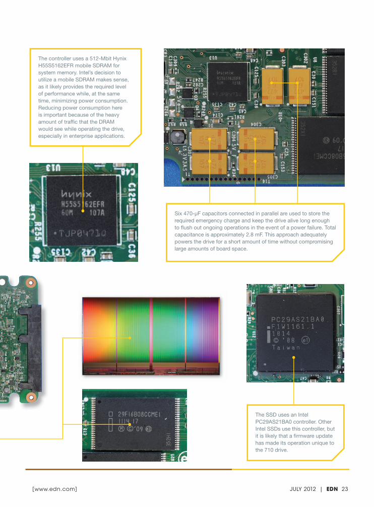
The controller uses a 512-Mbit Hynix H55S5162EFR mobile SDRAM for system memory. Intel’s decision to utilize a mobile SDRAM makes sense, as it likely provides the required level of performance while, at the same time, minimizing power consumption. Reducing power consumption here is important because of the heavy amount of traffic that the DRAM would see while operating the drive, especially in enterprise applications.
The SSD uses an Intel PC29AS21BA0 controller. Other Intel SSDs use this controller, but it is likely that a firmware update has made its operation unique to the 710 drive.
Six 470-µF capacitors connected in parallel are used to store the required emergency charge and keep the drive alive long enough to flush out ongoing operations in the event of a power failure. Total capacitance is approximately 2.8 mF. This approach adequately powers the drive for a short amount of time without compromising large amounts of board space.
[ www.edn.com ] JULY 2012 | EDN 23

MECHATRONICS IN DESIGNMECHATRONICS
DE
FE
NS
E S
YS
TE M
S C O N S U M E R P R O D U C T S MA
N
UF
AC
TU
RI N
G
ControlSystems
Software ElectronicSystems
MechanicalSystems
Digital ControlSystems
ControlElectronics
MechanicalCAD
Electro-mechanics
MA
TE
RI
AL
S P
RO
CE
SS
I NG
A U T O M O T I V E A E R O S P A C E ME
DI C
AL
XE
RO
GR
AP
HY
mechatronics
FRESH IDEAS ON INTEGRATING MECHANICAL SYSTEMS, ELECTRONICS, CONTROL SYSTEMS, AND SOFTWARE IN DESIGN
It is being talked about everywhere. “Harvard, MIT to Partner to Offer Free Online Courses,” The Boston Globeheralded on May 3. “The Campus Tsunami,” David Brooks
of The New York Times proclaimed on the same day. Stanford University president John Hennessy, interviewed in the May 2012 IEEE Spectrum, foresees “the death of the lecture hall as university education moves online.” The cover story of the summer 2012 ASEE Prism magazine reports a rekindling of the debate on the necessity of a master’s degree for engi-neers; meanwhile, the ASEE has just released its 2012 report, “Innovation with Impact.” It is clear that the industry warn-ing “innovate or perish” applies to education as well, and it is time for action, not just talk.
I have heard it said that it is easier to move a cemetery than it is to change an engineering curriculum. Engineering schools for which that is true might soon be buried in those cemeteries. If information is a commodity—as I believe it now is—and if all engineering schools do is deliver traditional course content in a lecture format, then those schools will cease to exist, because that type of education has little impact on student learning and performance.
In engineering design, adding a sophisticated controller to a poor-ly designed physical system will never get it to offer outstanding performance. Similarly, tradition-al course content, even if the best lecturers in the world deliver it online, is still just information—a commodity. The problem is not the delivery method; the problem is the content of the delivery.
Engineering content must be rebundled and integrated with a balance between theo-ry and industry best practices. Information thus becomes knowl-edge, which is not a commodity. Such knowledge stimulates stu-dents and transforms them into
critically thinking problem solvers, yielding a competitive advantage in the global economy.
Though the challenges for engineering education are being talked about everywhere, the only way to solve them is to change the culture, rejecting silos and comfort zones and instilling ownership. Until engineering education is viewed as an equal partner with engineering research in achieving innovation, that change will not happen.
A new concept for graduate-level education is emerging that could be applied to undergraduate education as well (Figure 1). It involves the creation of integrated, one-credit fundamental modules, delivered online. Such a structure works well for practicing engineers who must take courses part-time and who often find it easier to devote five weeks of intense effort to learning while working, instead of the typical 15 weeks of protracted study.
Once the modules have been completed, four three-credit online systems courses are taken that build on the modules. These stimulating, relevant, rewarding courses bridge fun-
damentals with actual practice. A six-credit onsite culminating experience completes the degree requirements.
The key is the integration and balance of theory with industry best practices. Such content does not exist in any one place; it must be gathered and integrated. Innovative industry leaders with passion will lead the way.
I am collaborating now with just such a leader to create a pro-gram in the area of fluid-power systems and control. Tom Price, president of Price Engineering, recognizes the value of this approach for his company, its workforce, his customers, and the United States. We need more industry leaders willing to step up and do the same.EDN
Engineering education upheavalInformation is a commodity; balancing and integrating information are not.
24 EDN | JULY 2012 [ www.edn.com ]
Figure 1 A new education concept comprises the creation of integrated one-credit fundamental modules, delivered online. The structure works well for practicing engineers who must take courses part-time and who often find it easier to devote five weeks of intense effort while working, instead of the typical 15 weeks of study.
By Kevin C Craig, PhD
INTEGRATION
SIX-CREDITONSITE
CULMINATINGEXPERIENCE
FOUR THREE-CREDITONLINE COURSES
12 ONE-CREDITONLINE MODULES
BALANCETHEORY
UNIVERSITYACADEMIC
RIGOR
INDUSTRYBEST
PRACTICES
PRACTICE
EDN1207MECH Fig 1.eps

Your FIRST CHOICEfor Performance
for more information call 1.800.981.8699 or visit us at www.irf.com
BVDSS Package
Max. RDS(on) @
Part Numbers4.5V(mΩ)
2.5V(mΩ)
-20VPQFN 2x2 31 53 IRLHS2242
SOT-23 54 95 IRLML2244
20V
PQFN 2x2 11.7 15.5 IRLHS6242
SOT-23 21 27 IRLML6244
Dual PQFN 2x2 45 62 IRLHS6276
30V
PQFN 2x2 16 20 IRLHS6342
TSOP-6 17.5 22 IRLTS6342
SOT-23 29 37 IRLML6344
Dual PQFN 2x2 63 82 IRLHS6376
Features
• Available in both N & P Channel for simple design
• Latest silicon technology offering low RDS(on) for increased battery life
• 2.5V drive capable available for 1-cell Li-Ion Battery Applications
• PQFN package offers high power density reducing system size
Applications
• DC Load Switch
• Battery Protection
• DC-DC Converter
• Screen Backlight Boost Converter
Small Power MOSFETs Designed for Handheld Devices
Gate Drive - 4.5V Optimized, 2.5V Capable, 12V Maximum
BVDSS Package
Max. RDS(on) @
Part Numbers10V(mΩ)
4.5V(mΩ)
-30V
PQFN 2x2 37 60 IRFHS9301
SOT-23 64 103 IRLML9301
Dual PQFN 2x2 170 290 IRFHS9351
25VPQFN 2x2 13 21 IRFHS8242
SOT-23 24 41 IRFML8244
30V
PQFN 2x2 16 25 IRFHS8342
TSOP-6 19 29 IRFTS8342
SOT-23 27 40 IRLML0030
Gate Drive - 10V Optimized, 4.5V Capable, 20V maximum
up to 2 A
up to 4 A
up to 7 A
up to 10 A
PQFN 2x2 Dual
SOT-23
TSOP-6
PQFN 2x2
up to 7 A
up to 10 A
Extend Battery Life With IR's Benchmark MOSFETs
THE POWER MANAGEMENT LEADER

www.caplugs.com • 1-888-CAPLUGS
You make the connection. We provide the protection.Protect your connectors, pins and leads from dust, moisture and impact damage with our full line of caps and plugs. Choose from hundreds of styles and sizes that are in-stock and ready to ship.
• Wide range of materials
• Certified to meet MIL/NAS specs
• Comprehensive custom capabilities
If we don’t have it, we’ll make it. We have a team of design engineers and in-house tool room dedicated to the development and production
of custom parts to meet our customers’ specific needs.
Visit us at www.caplugs.com or contact a technical sales specialist at 1.888.CAPLUGS.
We’ve got everything covered.SM

ima
gE
: iS
TO
CK
an
d S
hu
TT
Er
ST
OC
K
A utomotive start-stop operation, which reduces idling by shutting down a car’s engine when the car momentarily stops, is a simple concept that can go a long way toward improving fuel econ-omy and cutting emissions. The ICE (internal-combustion engine) system remained the pre-
dominant technology for vehicle propulsion among the roughly 80 million cars produced worldwide in 2011. Global trends, however, are conspiring to shift the balance toward alterna-tives. On one hand, the price of gasoline has skyrocketed; on the other, legislation governing emission standards is becoming more stringent worldwide.
Packaging and circuit integration deliver imProved Performance for start-stoP automotive aPPlications.
By masashi sekine and Jifeng Qin • international rectifier corP
July 2012 | EDN 27[ www.edn.com ]
AdvAnced power switches boost microhybriD EmissioNs gaiNs

28 EDN | JuLY 2012 [ www.edn.com ]
In Europe, vehicle carbon-dioxide emissions are subject to a voluntary agreement between the European Union and automakers, but legislation has been pushed because overall perform-ance remains way off the voluntary goal. Meanwhile, the Euro 6 standard, which requires substantial reductions in oxides of nitrogen emissions, will be phased in over the next few years. These developments ratchet up the challenges confronting automakers as they work to conform to evolving standards.
Clearly, reducing fuel consumption is one key to meeting the stringent new requirements. Toward that end, the market will boom in the next 10 years for HEVs (hybrid-electric vehicles) of all configurations—micro, mild, full, and plug-in—as well as for full EVs. Adoption of HEVs and EVs will be critical for meeting carbon-dioxide emissions targets for 2020.
Research firm Yole Développement predicts that combined HEV/EV demand will increase this decade at a compound annual rate of 31% to reach 50 million cars in 2020, or about 50% of all cars produced that year (Figure 1).
Analysts expect microhybrid vehicles to account for most of that volume.
Hybrid typesThe major difference between micro-hybrid systems and full- or plug-in-hybrid systems is that microhybrids lack an electric powertrain to propel the vehicle. Rather, the microhybrid’s start-stop system shuts down and restarts the ICE to reduce the amount of time the engine spends idling, such as when a car is sitting at a traffic light or in a traffic jam. The mild hybrid has a regenera-tive braking system in addition to the start-stop feature. Fuel-economy gains from these technologies are typically in the range of 5% to 10% compared with conventional vehicles’ fuel-economy numbers (Table 1).
Various start-stop systems are avail-able. One is the super starter, which uses a rugged dc starter plus a battery-
management system. With a low, $80 average cost to the end user, super start-ers hold an estimated two-thirds of the total market for start-stop systems. Car manufacturers adopting the technology include BMW.
Another start-stop system is the BAS (belt-driven alternator starter), featuring a dc-ac inverter with average power typi-cally in the 1.5- to 3-kW range. Such systems are virtually silent and offer an engine-restart time as low as 400 msec. With an estimated end-user price of approximately $300, BAS systems are found in many midpriced vehicles.
Finally, for conditions of extreme cold that can compromise the operation of conventional start-stop systems, a dual-battery solution or a dc-dc boost solution can be used to maintain the bus voltage.
two batteriesIn a typical dual-battery technology, when the ICE is running, power switch Q1remains on so that the load
at a GLaNCe↘ Stopping the internal-combus-tion engine when a vehicle is not moving is a cost-effective method of cutting fuel use and emissions.
↘ Start-stop can be accomplished with dual batteries or with a battery and boost converter that stores energy in an inductor.
↘ Specialized battery power switches are available that discon-nect the starter and main battery from the auxiliary electrical systems during engine start.
Figure 1 HEV/EV demand is forecast to increase 31% annually through 2020 (courtesy Yole Développement, August 2011).
UNITS (M)
2009 2010 2011 2012 2013 2014 2015 2016 2017 2018 2019 2020
MICROMILD HYBRID EV
PLUG-IN HYBRID
FULL HYBRID
MILD HYBRIDMICROHYBRID
EDN120712DF Fig 1.eps DIANE
0
5
10
15
20
25
30
35
40
45
50
55
60
TAblE 1 HEV typEs by function
FunctionMicrohybrid/
micromild hybrid Full hybrid Plug-in hybrid
Start-stop Yes Yes Yes
Regenerative braking Yes (micromild only) Yes Yes
Electric drive No Yes Yes
Recharge on grid No No Yes
Fuel savings (%) 5 to 10 25 to 40 50 to 100

is fully supplied by the main battery as well as an alternator (Figure 2). When the vehicle stops, the ICE turns off, and the main battery becomes the only source of power supply to the load. At engine restart, the main-battery voltage must supply a transient current as high as 1000A to the starter motor, resulting in a transient-voltage drop at the main-battery terminal to as low as 6V.
To prevent the power-electronics circuit from shutting down due to the battery-cranking transient event, a controller sends a turnoff signal to Q1 to disconnect the main battery from the load. The auxiliary battery then supplies power to the load and maintains the battery voltage. After the engine restarts successfully and the alternator resumes operation, Q1is turned on and the system reenters vehicle running mode.
Power switch Q1 and the control-ler are also used as a part of a reverse battery-protection circuit. If the main battery is connected in reverse polar-ity, Q1 stays off because no signal is coming from the controller. It protects circuitry on the load by terminating the reverse-current-flow path.
Dc-Dc boostA similar configuration uses a dc-dc boost converter instead of an auxiliary battery (Figure 3). At engine restart, bypass switch Q1 disconnects the main battery from the load, and a dc-dc con-verter supplies a boosted voltage to the load during the cranking period.
The dc-dc boost converter compris-es one inductor, two power switches (Q2 and Q3), and one output capaci-tor. All energy is stored at the inductor when Q2 turns on. Q3 would be off at that time. The inductor then transfers the energy to the load through Q3 when Q2 is off. The voltage on the main bat-tery and the voltage on the load termi-nal determine the duty cycle of Q2. A PWM controller operates this type of synchronous dc-dc boost converter in continuous-conduction mode to main-tain the voltage on the load terminal.
MicrohybriD exaMpleFor the battery switch, International Rectifier’s AUIRF1324S-7P surface-mount MOSFET delivers a maximum on-state resistance as low as 1 mΩ and an output current up to 240A. For
through-hole packaging requirements, the company offers the AUIRF1324L in a conventional TO-262 with a maxi-mum on-state resistance of 1.65 mΩ.
The wide-lead, TO-262-packaged AUIRF1324WL power MOSFET can reduce the maximum on-state resis-tance by roughly 20%. Wider-lead packages mean more areas fit the inter-nal wirebonds at the MOSFET’s source terminal. The lower on-state resis-tance and the improved wirebonding
inside the package collectively yield an approximately 30% increase in the maximum-drain-current rating.
All MOSFETs in the 24V 1324 family are suitable candidates for bat-tery-switch applications. IR also offers 40V automotive-grade MOSFETs with an on-state resistance as low as 1.25 mΩ. These products are suited for dc-dc-converter applications.
The AUIR3240S, an automotive-grade high-side MOSFET driver, drives
JULY 2012 | EDN 29[ www.edn.com ]
www.isipkg.com 805.482.2870 [email protected] and Manufactured in the U.S.A.
Reduce your concept-to-production cycle time with our multi-discipline design teams and vertically-integrated manufacturing.
You don’t need cell-phone production volumes to miniaturize & cost reduce your next designusing the latest packaging technologies.
3D & Advanced PackagingCost Effective at Any Quantity
Quick-Turn, On-Shore Capabilities
Stacked Die
Chip on Board
Hybrid Assembly
Package in Package
Package on Package
Optical-Die Packaging
System in Package
Multi-Chip Module
3D Packaging
Flip Chip

30 EDN | JULY 2012 [ www.edn.com ]
EDN120712DF Fig 3.eps DIANE
STARTER
ALTERNATOR
CONTROLLER
CONTROLLER
Q1
Q2
Q3
_
+VBATTERY
VBATTERY
VLOAD
VLOADRLOAD
14V
14V
6V
GATE Q1
GATE Q2
GATE Q3
EDN120712DF Fig 2.eps DIANE
STARTER ALTERNATOR CONTROLLER
Q1
_
+_
+VBATTERY
VBATTERY
VLOAD
VAUXILIARYVLOAD
RLOAD
14V
14V
6V
GATE Q1
Figure 2 Dual-battery switch technology in the microhybrid system uses an auxiliary battery to provide high starting currents for start-stop operations. During start, Q1 disconnects the main battery from the power-electronics circuit, to which the auxiliary battery then supplies the correct voltage.
Figure 3 The dc-dc boost converter topology in a microhybrid system stores energy in the converter inductor. Here the boost con-verter (dotted box) functions as the auxiliary battery in the dual-battery system.
EDN120712DF Fig 4.eps DIANE
NTC
NTC EN
RS NTC
RIN
R NTC
/IN
VDG IN
AUIR3240S
GND
100 nF
500 μH
GATE
VCC
SW
RS
RS
CURRENT MEASUREMENT
NTC
LOADSMAIN BATTERY
Figure 4 The dual-battery system can use the board-net stabilizer in the high-ly integrated AUIR3240S power-switch high-side MOSFET driver. The power switch disconnects the starter and bat-tery from auxiliary systems when the engine is started.
the battery power switch for start-stop applications (Figure 4). The highly integrated boost converter was designed specifically for start-stop systems, which require a board-net stabilizer that uses a power switch to disconnect the starter and main battery from the auxiliary electrical systems during engine start. The AUIR3240S can drive several MOSFETs in parallel to achieve very low on-state resistance, with current consumption of less than 50 μA. The device provides 15V on the output, with a wide input voltage of 4 to 36V. The AUIR3240S also features diagnostics on the output current and a thermal sensor interface for a robust design.
Continued development of micro-hybrid start-stop systems requires solu-tions for reducing the cranking voltage drop, integrating more electronics into the starter and furthering the evolu-tion of battery technologies. Power-electronics vendors and automakers are putting the components in place to make the necessary advancements.EDN
AcknowledgmentThis article originally appeared on EDN’s sister site, Automotive Designline, www.eetimes.com/4373749.
Authors’ b iogrAphiesMasashi Sekine is an appli-cations and technical mar-keting engineer in the Auto-motive Product business unit of International Recti-fier (El Segundo, CA). He
supports field activities related to MOS-FET-based automotive applications as well as product specifications and definitions. Sekine holds a bachelor of science degree in electrical engineering from Tokyo Institute of Technology and has 10 years of experi-ence in power electronics.
Jifeng Qin is a product man-ager in the Automotive Product business unit of In-ternational Rectifier. He holds a bachelor of science degree in electrical engineer-
ing from Zhejiang University (Hangzhou, Zhejiang, China) and a master’s degree in electrical engineering from North Carolina State University. Qin has more than five years of experience in circuit design, appli-cation, and marketing, and he holds seven US patents.
[ www.edn.com ]
ProtoMat® Benchtop PCB Prototyping MachineWhat would your day look like tomorrow if you couldcut yourself free from the board house and producetrue, industrial quality PCBs right at your desk?LPKF’s ProtoMat benchtop prototyping systems arehelping thousands of engineers around the worldtake their development time from days and weeks to minutes and hours. In today’s race to market, it’s like having a time machine.
www.lpkfusa.com/pcb1-800-345-LPKF
“You can’t beat an LPKF systemfor prototyping. We do up tothree iterations of a designwithin a day.”
Leonard WeberAgilent
9:00 AM
Your circuit design isdone and you’re readyto make a prototype.
11:48 AM
Why not try a differentapproach before youhead to lunch? 1:03 PM
Your second board isready to test.
3:14 PM
After a few tweaks,you’re ready to makeyour finished board.
4:09 PM
Your finished board isready to go.
5:00 PM
Nice work. You justshaved weeks off yourdevelopment schedule.
10:05 AM
Your first board isready to test.
microhybrid start-stop systems require solutions for reduc-ing the cranking voltage drop.

32 EDN | JuLY 2012 [ www.edn.com ]
Image sensors evolve to address
EmErging EmbEddEd-
vision nEEds

JULY 2012 | EDN 33
BY BRIAN DIPERT • EMBEDDED VISION ALLIANCE, AND ERIC GREGORI AND SHEHRZAD QURESHI • BDTI
Look at the systems you’re designing, or more generally at the devices that surround your life, and you’re likely to see a camera—or a few—staring back at you. Image sensors and their paired image processors are an increasingly common presence in a diversity
of electronic products.It’s nearly impossible to purchase a laptop com-
puter without a bezel-mount camera, for example, and a rising percentage of all-in-one desktop PCs, dedicated computer displays, and even televisions now include them as well. Smartphones and tablets, too, frequently feature image sensors, often located on both the front and back panels, and sometimes even arranged in “stereo” configurations for 3-D image cap-ture. You’ll even find cameras embedded in portable multimedia players and mounted in cars.
AS TECHNOLOGY PROGRESSES
FROM ELEMENTARY IMAGE CAPTURE
TO MORE ROBUST IMAGE ANALYSIS,
INTERPRETATION, AND RESPONSE,
SEMICONDUCTOR SUPPLIERS
AND THEIR OPTICS PARTNERS ARE
RESPONDING WITH IMPROVED
IMAGE-SENSOR SUBSYSTEMS.
IMA
GE
(S):
TH
INK
ST
OC
K
[ www.edn.com ]

ApplicAtion AbundAnceThe fundamental justification for including a camera in a design is often to enable elementary image capture, notably for still photography, videogra-phy, and videoconferencing. Given that the imaging building blocks are already in place, however, software and system developers are also leveraging them for more evolved purposes, such as discern-ing meaning from the content and tak-ing appropriate action in response to the interpreted information.
In the vehicle use case, for example, an advanced analytics system doesn’t just “dumbly” display the rearview cam-era’s captured video feed on an LCD but also warns the driver when it detects an object behind the vehicle. Advanced implementations might go so far as to slam on the brakes to preclude impact.
Additional cameras, mounted both inside the vehicle and in various loca-tions around it, alert the driver to—and, in advanced implementations, take active measures to avoid—unintended lane transitions and collisions with objects ahead. They can also discern road signs’ meanings and consequently alert the driver to excessive speed or potentially dangerous roadway condi-tions. The cameras further can mini-mize driver distraction by enabling gesture-interface control of the radio and other vehicle subsystems, and they can snap a dozing, texting, or otherwise multitasking driver back to full atten-tion to the road.
Smartphones, tablets, computers, and televisions employ front-mounted image sensors for diverse purposes. They can alert a user who is sitting too close to or too far away from the display, or whose posture is poor. They can ensure that the display backlight stays on as long as a person is positioned in front of the display, and, conversely, they can auto-power down the display when the person steps away. Gesture interfaces play an increasingly important role in these and other consumer-electronics
applications, such as game consoles, supplementing—if not supplanting—such traditional mechanisms as button and key presses or trackpad or mouse swipes and clicks.
A forward-facing camera can moni-tor respiration, by measuring chest rise-and-fall cadence, and heart rate, by detecting the minute, cyclical vari-ance in facial color caused by blood flow. It can monitor eyeball drift to warn a user who has had too much to drink. It can identify an authorized user who appears in front of a system, auto-matically logging in that person and loading account-specific programs and settings. A rear-mount camera, mean-while, can employ augmented reality to supplement the conventional view of an object or scene with additional information.
These examples typify embedded vision, a burgeoning application cat-egory that extends to dedicated-func-tion devices such as surveillance sys-tems and manufacturing-line inspection equipment. In some cases, computers running PC operating systems histori-cally handled the vision-analytics task, although such approaches were costly, bulky, high-power, and unreliable. In other situations, any or all of those same
factors made it inherently impractical to implement vision functionality.
Now, with the increased perform-ance, decreased cost, and reduced power consumption of processors, image sensors, memories, and other semiconductor devices, developers are evaluating embedded-vision capabili-ties for a diversity of system form fac-tors and price points. That activity has also prompted the need for increasingly robust imaging subsystems (see sidebar “Focus: the fourth dimension,” avail-able online at http://bit.ly/PPlwEe).
RAnge veRsus ResolutionFor many years, a “more megapixels is better” mentality fueled the consumer digital-camera market, whose con-stituent image sensors—by virtue of their high volumes and consequently low prices—also find homes in many embedded-vision systems. In recent times, however, the limitations of such a simplistic selection strategy have become progressively more apparent.
For one thing, consumers increas-ingly realize that unless they’re printing wall-sized enlargements or doing tight crops of a source photo, they don’t need high-resolution images, which take up significantly more storage space than their lower-resolution precursors. For another, the noisy and otherwise arti-fact-filled images that modern cameras generate reveal the lithography-driven downside of the increasing-resolution trend.
Sensors must remain small in over-all dimensions to remain cost-effec-tive—a critical attribute in consumer-electronics systems. As manufacturers shoehorn an increasing number of pixels onto sensors, individual pixel dimensions must therefore predictably shrink. Smaller pixels collect fewer photons in a given amount of time, thereby leading to decreased light sen-sitivity. That phenomenon not only degrades a camera’s low-light perform-ance but also adversely affects the sys-tem’s dynamic range. Postprocessing can only partially compensate for that compromise, and then often only with motion artifacts and other trade-offs (see Part 2 of this article, “HDR pro-cessing for embedded vision,” available online at www.edn.com/4375325).
Ironically, embedded-vision-focused applications tend to have lower resolu-
34 EDN | JuLY 2012 [ www.edn.com ]
At A glAnce↘ With the increased performance, decreased cost, and reduced power consumption of processors, image sensors, memories, and other semi-conductor devices, developers are evaluating embedded-vision capa-bilities for a diversity of system form factors and price points.
↘ A conventional image-sensor-based design can support many embedded-vision implementations, but for depth-cognizant require-ments, a 3-D image-sensor subsys-tem is often necessary.
↘ Common methods for depth mapping are stereo sensor arrays, which “bolt” together two cameras; structured light, which projects a predetermined light pattern onto a scene for analysis; and time of flight, which derives range from the time it takes for projected light to travel from the source to the object and back to the sensor.
oNliNE ExclusivEPart 2 of this article, available exclusively online, discusses HDR processing for embedded vision. Read it at www.edn.com/4375325.

Promoting the real benefi ts of authorized sourcingwww.eciaonline.org • www.carltonbates.com

tion requirements than does general-purpose photography. The infrared- and visible-light image sensors in Microsoft Corp’s Kinect, for example, are VGA (640×480-pixel) resolution models, and the vision peripheral passes only along QVGA (320×240-pixel) depth-map images to the connected game console or PC.
Given the plethora of available pixels in modern sensors, some sup-pliers leverage the surplus to improve both light sensitivity and color accu-racy by migrating beyond the conven-tional Bayer RGB-pattern filter-array approach (Figure 1). Additional—and altered—filter colors are claimed to enhance full-spectrum per-pixel inter-polation results, whereas monochrome, or filterless, pixels let in even more light, at the trade-off of dispensing with color discernment (Reference 1).
Leica Camera AG’s latest digital still camera takes filter alteration to the extreme, capturing only black-and-white images by virtue of its filterless monochrome image sensor (Figure 2a). Reviewers, however, espouse the sharp-ness of the camera’s photographs even at high ISO settings.
Meanwhile, Nokia Corp’s 808 PureView smartphone embeds a 41M-pixel image sensor but by default outputs 8M-pixel or lower-resolution images (Figure 2b and Reference 2). By combining multiple pixels in vari-ably sized clusters depending on the digital zoom setting, the 808 PureView dispenses with the need for a complex, costly, and bulky optical zoom structure and multiplies the effective per-image-pixel photon-collection capability for improved low-light performance.
Sony Corp has pioneered a sensor-design technique called backside illu-mination (Figure 2c). Implementation specifics aside, the technique routes the interpixel wiring behind the pixels’ photodiodes to improve a sensor’s per-pixel fill factor—the percentage of total area devoted to light collection—and therefore its low-light capabilities.
DEPTH DISCERNMENTA conventional image-sensor-based design can support many embedded-vision implementations. It can, for example, assist in interpreting elemen-tary gestures, as well as tackle rudi-mentary facial-detection and -recog-
nition tasks, and it is often adequate for optical-character-recognition func-tions. It might not, however, cleanly detect elaborate gestures that incorpo-rate movement toward or away from the camera (3-D), as opposed to ges-tures strictly in the vertical and hori-zontal planes (2-D). More generally, it cannot fully discern the entirety—that is, the depth—of an object; for example, it cannot easily distinguish between a person’s face and a photo-graph of that person. For such depth-cognizant requirements, a 3-D image-sensor subsystem is often necessary (Reference 3).
Regardless of the specific 3-D sensor implementation, the common output is the depth map, an image matrix in which each pixel-data entry—which is sometimes additionally color-coded for human-interpretation purposes—represents the distance between the sensor and a point in front of the sensor (Figure 3). Each depth-map frame commonly mates with a corre-sponding frame captured by a conven-tional 2-D image sensor, with the two frames parallax-corrected relative to each other because they source from
36 EDN | JULY 2012 [ www.edn.com ]
Figure 1 The Bayer sensor pattern, named after a Kodak imaging scientist, remains the predominant filter-array scheme used in digital imaging applications (a). More modern approaches increase the number of green-spectrum pixels in a random pattern for enhanced detail in this all-important portion of the visible-light spectrum (b), leverage subtractive colors—at the trade-off of greater required postprocessing—in order to improve the filters’ light-transmission capabilities (c), and even add filterless mono-chrome pixels to the mix (d).
(a)
(d)
(b) (c)
A CONVEN-TIONAL IMAGE-SENSOR-BASED DESIGN CAN ASSIST IN INTER-PRETING ELEMEN-TARY GESTURES.

DC to 2 GHz
Stanford Research SystemsTel: 408-744-9040
www.thinkSRS.com
RF Signal Generator
... $3900
Model SG382
Aff ordable RF Signal Generators
... only from SRS !
• DC to 2GHz sine waves• AM, FM, ΦM, PM & sweeps• Excellent phase noise• Ethernet, GPIB & RS-232• Unbeatable price
Introducing a new line of a� ordable RF signal generators from SRS!
Why pay two or three times as much for an instrument from Agilent? The SG382 o� ers a wide frequency range of DC to 2 GHz, performs full octave frequency sweeps, and comes loaded with all the performance and features you’ll need.
SG382 third_prim_red_CMYK.indd 1 1/4/2012 12:09:48 PMSRS RESIZE.indd 1 7/11/12 11:39 AM
separate cameras in separate locations. One common method of discerning
depth is by means of a stereo sensor array, which arranges two image sensors in a configuration reminiscent of a pair of eyes. As with the human brain and eyes, an imaging SOC processes the sen-sors’ differing-perspective viewpoints of an object to assess the distance between the object and the sensor array. It’s pos-sible to extend the concept beyond two sensors in multiview-geometry applica-tions. The dual-sensor approach is often the lowest-cost, lowest-power-consump-
tion, smallest-form-factor option, and it’s particularly attractive if the sensors are already present in the design for 3-D still-image photography and video capture.
One stereo-imaging implementation is the discrete “binocular” approach, achieved by “bolting” together two cameras. Although this version of the concept may be the most straightfor-ward from a hardware standpoint, the required software support is more com-plex. By way of analogy, two motor-cycles linked together with a common
FRONT-ILLUMINATED STRUCTURE
BACK-ILLUMINATED STRUCTURE
INCIDENT LIGHT
2.2 μM
M1M2
METAL WIRING
METAL WIRING
BACK SIDE
SI SUBSTRATE
SI SURFACERED GREEN
LENSESCOLOR FILTER
METAL WIRING
MICROLENSESCOLOR FILTERS
METAL INTERCONNECTS
PHOTOSENSITIVELAYER
SUBSTRATE
LIGHT-RECEIVING SURFACE
COLOR FILTER
ON-CHIP LENS
ON-CHIP LENS
SUBSTRATEPHOTO-DIODE
PHOTODIODE
PHOTODIODE
Figure 2 Leica’s M Monochrom will set you back $8000 or so and captures only black-and-white images, but reviewers rave about the camera’s sharpness and low-light performance (a). The Nokia 808 PureView smartphone packs an enormous, 41M-pixel image sensor, which it uses to implement digital zoom and clustered-pixel photon-collection capabilities (b). A Sony-pioneered sensor-design technique called backside illumination routes the interpixel wiring behind the photodiodes, thereby improving the per-pixel fill-factor ratio (c).
(a)
(c)
(b)
[ www.edn.com ]

38 EDN | JuLY 2012 [ www.edn.com ]
(a)
(b)
(c)
(d)
Stay connected and informed with EDN on LinkedIn, Facebook, and Twitter.
EDN ’s Electronics Design Network group is the essential LinkedIn group for the full spectrum of information needed by design engineers, engineering managers, and upper management through each phase of the design cycle, from product-concept development to the manufacturing of electronics.
Become a fan of EDN on Facebook and join in discussions with your peers, keep track of industry events, and stay on top of news and trends.
Follow EDN on Twitter for real-time news updates, technical analysis, and quick tweets on our blogs, editors, and opportunities.
➜ To join, log on to LinkedIn and type in “EDN’s Electronics Design Network” under “Groups.”
➜ To join, go to Facebook and type in“EDN: Voice of the Engineer.”
➜ @EDNmagazine
Stay connected and informed with Stay connected and informed with EDN on EDN on EDN
Want to know what is important to your
peers right now? Have an opinion
you want to get off your chest?
How about a pesky design question that
another engineer may be able to answer?
Thousands of engineers and executives are already exchanging ideas with fellow EDN readers through LinkedIn, Facebook, and Twitter. Join the conversation!
EDN_1105042 Print Ad Social Media0.5H.indd 1 6/9/11 11:11 AM
Figure 3 Regardless of the specific 3-D camera technique employed, they all out-put a depth map of objects they discern (a). A device such as the HTC EVO 3-D smartphone, whose stereo sensor array is primarily intended to capture 3-D still and video images, can also be used for 3-D embedded-vision purposes (b). Microsoft’s Kinect (c) harnesses the structured-light method of discerning depth by projecting a known infrared-light pattern in front of it and then analyzing the shape and orienta-tion of the ellipses that it sees (d).

axle do not make a car. The cameras require calibration for robust image registration, and their frames must be synchronized if—as is commonly the case—either the camera array or the subject is moving.
Alternatively, it’s possible to com-bine two image sensors in a unified SOC or multidie package, output-ting a combined data stream over one bus. The advantages of the fully integrated approach include improved control and frame synchronization. The tighter integration improves cali-bration, which in turn yields better stereo-imaging results, manifested as increased depth perception and faster image processing.
Projection aPProachesStructured light, the second common 3-D sensor scheme and the technology used in Microsoft’s Kinect, projects a predetermined pattern of light onto a scene for the purpose of analysis. The structured-light method’s 3-D sensor scheme uses a projector to create the light pattern and a camera to sense the result.
In the case of the Kinect, the projec-tor employs infrared light. Kinect uses an astigmatic lens with different focal lengths in the x and y directions. An infrared laser behind the lens projects an image comprising a large number of dots that transform into ellipses, whose particular shape and orientation in each case depend on the object’s distance from the lens.
Advantages of the structured-light approach include its finely detailed resolution and its high accuracy, nota-bly in dimly illuminated environments where visible-light spectrum-focused image sensors might struggle to capture adequate images. Structured-light soft-ware algorithms are also comparatively simple compared with the stereo sensor approach, although the concomitant point-cloud processing can be compu-tationally expensive, approaching that of stereo vision.
Conversely, the structured-light technique’s reliance on infrared light, at least as manifested in the Kinect, means the technology will have issues operating outdoors, where ambient infrared illumination in sunlight will destructively interfere with the light coming from the projector. The projec-
tor is also costly and bulky, consumes substantial power, and generates a large amount of heat; indeed, Kinect con-tains a fan specifically for this reason (Reference 4). The necessary custom projector lens adds to the total bill-of-materials cost.
Time of flight is the third common method of implementing a 3-D sensor. As with structured light, a time-of-flight camera contains an image sen-sor, a lens, and an active illumination source. With time of flight, however, the camera derives range, or distance, from the time it takes for projected light to travel from the transmission source to the object and back to the image sensor (Reference 5). The illu-mination source is typically either a pulsed laser or a modulated beam, depending on the image-sensor type that the design uses.
Image sensors that integrate digital time counters typically combine with pulsed laser beams, as do shutter-inclu-sive range-gated sensors. In the latter case, the shutter opens and closes at the same rate with which the projector emits the pulsed beam. The amount of light each image-sensor pixel “sees” is therefore related to the distance the pulse traveled, hence the distance from the sensor to the object. Time-of-flight designs that include image sensors with phase detectors conversely use modulated-beam sources. The strength of the beam varies over time, and so measuring the incoming light’s phase indirectly derives the time-of-flight distance.
Time-of-flight cameras are common in automotive applications, such as pedestrian detection and driver assis-tance, and are equally prevalent in robotics products. They also have a long and storied history in military, defense, and aerospace implementa-tions. The required image-processing software tends to be simpler, and there-fore more real-time-amenable, than the requisite software for stereo cam-era setups, although the time-of-flight technique’s susceptibility to ambient-
Stanford Research SystemsTel: 408-744-9040
www.thinkSRS.com
DC to 4 GHz
RF Signal Generator
... $4600
Model SG384
Versatile RF Signal Generators
... only from SRS !
• DC to 4 GHz sine waves• AM, FM, ΦM, PM & sweeps• Excellent phase noise• Standard OCXO timebase• Square wave outputs
When it comes to versatility, the SG384 Signal Generator delivers!
The SG384 o� ers 1 µHz resolution from DC to 4 GHz, performs full octave frequency sweeps, and comes equipped with an OCXO timebase.
Its low phase noise and excellent frequency stability allow the SG384 to produce very pure output sine waves.
Options include I/Q modulation inputs, square wave clock outputs, a frequency doubler, and an atomic rubidium timebase.
SG384 third_prim_green_CMYK.indd 1 1/4/2012 12:13:03 PMSRS RESIZE.indd 3 7/11/12 11:39 AM
Join The conversaTionTo comment on this article, go to www.edn.com/4375300.
[ www.edn.com ]

Get current, without the hassle.
Design News is a registered trademark of UBM plc © 2012
REGISTER AT
DesignNews.com/dkcec
With Digi-Key’s Continuing Education Center, catch up to 180 days of free,
interactive courses engineered by Design News, starting January 2012.
Build your engineering know how. Take one or all. It’s your choice.
Tracks include: Microcontrollers Basic, Microcontrollers Advanced, MEMS Sensor
Technology, Lighting, Embedded Internet and Cloud, Wirelesss, and Power.
@DigiKeyCEC
Digi-Key Continuing Education Center
FOLLOW US

illumination interference and multiple reflections somewhat complicates the algorithms.
Frame rates for time-of-flight approaches can be quite high—upward of 60 frames per second, a speed that’s difficult to achieve with stereo imager setups—but the comparative resolu-tion is usually lower. And, as with the structured-light technique, the required time-of-flight light projector translates into cost, power consump-tion (and heat dissipation), size, and weight downsides.
AlliAnce, design successEmbedded-vision technology has the potential to enable electronic prod-ucts that are more intelligent and responsive, and thus more valuable to users, than ever before. The tech-nology can add helpful features to existing products, and it can provide significant new markets for hardware, software, semiconductor, and systems manufacturers.
The Embedded Vision Alliance, a worldwide organization of technology developers and providers, was formed last summer to provide engineers with the tools necessary to speed the trans-formation of this potential into reality. The mission of the alliance is to provide practical education, information, and insights to help engineers incorporate embedded-vision capabilities into prod-ucts (see sidebar “The Embedded Vision Alliance,” available online at http://bit.ly/M0GxrI).EDN
RefeRences1 Embedded Vision Alliance, “Selecting and Designing with an Image Sensor: The Tradeoffs You’ll Need to Master,” http://bit.ly/LcEdRf.2 Embedded Vision Alliance, “Nokia’s 808 PureView: A Technical Article and Several Videos For You,” March 5, 2012, http://bit.ly/LxiOln.3 Embedded Vision Alliance, “March 2012 Embedded Vision Alliance Summit Technology Trends Presentation on Image Sensors,” http://bit.ly/Nfctdn.4 Ifixit, “Microsoft Kinect Teardown,” http://bit.ly/LcEy6y.5 Embedded Vision Alliance, “Time of Flight: Samsung’s New RGB Image Sensor Also Has Depth Sight,” March 1, 2012, http://bit.ly/N5abtU.
AuthoRs’ b iogRAphiesBrian Dipert is editor-in-chief of the Embedded Vi-sion Alliance. He is also a senior analyst at BDTI, a source of analysis, advice, and engineering for embed-
ded processing technology and applica-tions, and editor-in-chief of InsideDSP, BDTI’s online newsletter dedicated to dig-ital-signal-processing technology. Dipert has a bachelor’s degree in electrical engi-neering from Purdue University (West Lafayette, IN). He began his career at Magnavox Electronics Systems (Fort Wayne, IN), and subsequently spent eight years at Intel Corp (Folsom, CA) as well as 14 years at EDN.
Eric Gregori is a senior soft-ware engineer and embed-ded-vision specialist with BDTI. He is a robot enthu-siast and has more than 17 years of embedded-firm-
ware design experience. Gregori’s special-ties are computer vision; artificial intelli-gence; and programming for the Windows Embedded CE, Linux, and Android op-erating systems. He created the Robot Vi-sion Toolkit and developed the RobotSee Interpreter. Gregori is working toward his master’s degree in computer science. He holds 10 patents in industrial automation and control.
Shehrzad Qureshi is a senior engineer with BDTI and principal of Medallion So-lutions LLC. He has a master’s degree in computer engineering from Santa
Clara University in California and a bachelor of science degree in computer sci-ence from the University of California, Davis. He is an inventor or co-inventor on eight US-issued patents and has more pending. Qureshi earlier in his career was director of software engineering and act-ing director of IT at Restoration Robotics; before that, he was the software manager at biotech start-up Labcyte. He has held individual-contributor positions at Ac-curay Oncology, where he worked in med-ical imaging, and Applied Signal Technol-ogy, where he worked on classified signals-intelligence defense programs. Qureshi is the author of Embedded Image Pro-cessing on the TMS320C6000 DSP (Springer, 2005).
jULY 2012 | EDN 41[ www.edn.com ]Stanford Research Systems
Tel: 408-744-9040 www.thinkSRS.com
DC to 6 GHz
RF Signal Generator
... $5900
Model SG386
High Performance RF Sources
... only from SRS !
• DC to 6 GHz sine waves• Versatile modulation• −116 dB/Hz phase noise (1 GHz, 20 kHz o� set)
• ±0.002 ppm stability• Unbelievable value
The SG386’s price to performance ratio is truly remarkable. Its unique design architecture, OCXO timebase, and low phase noise allow you to generate the most stable, spurious-free sine waves possible — and it sells for about 1/3 the price of competitive instruments.
The SG386 comes loaded with features including modulation functions and computer interfaces. Options include square wave clock outputs, analog I/Q inputs, a frequency doubler, and an atomic rubidium clock.
SG386 third_prim_blu_CMYK.indd 1 1/4/2012 11:49:00 AMSRS RESIZE.indd 2 7/11/12 11:39 AM

Most of the latest three-axis digital micro-electromechanical-system accelerometers on the market can generate interrupts for a number of applications. Some of the appli-cations, including screen rotation, wake-up, free-fall, and single- and double-click
recognition, are popular, and designers have implemented them in various devices.
A digital MEMS accelerometer usually has one or two interrupt-output pins that can be interfaced with the I/O pins of an external host processor. You can configure the accelerometer to monitor acceleration or motion in the back-ground or simply to stay in low-power, sleep mode while the host processor performs other tasks. When the accelerometer detects an interrupt, the host processor can then wake up to check whether the interrupt needs to be served.
Data-reaDy interruptYou can configure a digital MEMS accelerometer to generate a signal to indicate when a new set of measurement data is available for reading. The data-ready bit in the status register of the accelerometer, which is accessible to users, usually represents this signal. You can route the signal to an inter-
rupt pin by enabling the data-ready interrupt bit in one of the control registers, and you can set its polarity to active-low or active-high through the edge-level bit in another control register. By default, the interrupt pin is active-high when the accelerometer powers up.
The data-ready interrupt signal goes high when a new set of acceleration data has been generated in the data registers of the accelerometer. The interrupt goes low when the system has read the high bytes of the data registers of all enabled axes. If the system has not read the high bytes during one output-data-rate period, then the data-ready interrupt will remain high, and the overrun bit in the status register becomes one. In this case, data overrun has occurred, and the system has overwritten the previous data samples.
You can use the data-ready interrupt feature to synchronize continuous data acquisition and prevent data loss. By default, the interrupt pin is a push-pull topology, which can be tied directly to a host-processor I/O port that has an interrupt function. When new data is not ready, the host processor can perform other tasks or simply stay in sleep mode.
Once the data-ready interrupt occurs, the host processor can wake up at the rising edge of the I/O port to enter the interrupt-service subroutine and then read and process the
acceleration data. That action can help reduce the overall system power consumption because it relieves the host processor of the task of continu-ing to poll the data-ready bit in the status register. During accelerometer evaluation, you can use the data-ready interrupt to check the frequency of the interrupt signal’s waveform at different output-data rates by using an oscilloscope.
Free-Fall interruptAccelerometer designers widely use the devices’ free-fall interrupt feature in hard-disk-protection applications. When, for example, a laptop computer is falling, the laptop computer’s embedded acceler-ometer can generate an interrupt so that the hard drive can park the magnetic head of the disk in a safe place to prevent mechanical damage to the disk.
Designers of medical systems can also integrate the accelerometer’s free-fall interrupt with a MEMS
Applying the interrupt features of MEMS accelerometers
By Jay Esfandyari, GanG Xu, and Paolo BEndiscioli • sTMicroElEcTronics
UndErStAnd how to iMplEMEnt rEliAblE And robUSt intErrUpt-bASEd ApplicAtionS USing MEMS-bASEd AccElEroMEtErS.
Figure 1 the accelerometer’s evaluation board and its windows demo software capture the device’s raw data and the interrupt signal.
42 EDN | JuLY 2012 [ www.edn.com ]

42V, 2.5A Synchronous Step-Down Regulator with 2.5µA Quiescent CurrentDesign Note 504
Hua (Walker) Bai
07/12/504
Figure 1. LT8610 12V to 3.3V Application Achieves High Effi ciency
Introduction
The LT®8610 and LT8611 are 42V, 2.5A synchronous step-down regulators that meet the stringent high input voltage and low output voltage requirements of automotive, industrial and communications applica-tions. To minimize external components and solution size, the top and bottom power switches are integrated in a synchronous regulator topology, including internal compensation. The regulator consumes only 2.5μA quiescent current from the input source even while regulating the output.
High Effi ciency Synchonous Operation
Replacing an external Schottky diode with an internal synchronous power switch not only minimizes the solu-tion size, but also increases effi ciency and reduces power dissipation. The effi ciency improvement is signifi cant in low output voltage applications where the voltage drop of the Schottky diode represents a relatively large portion of the output voltage. Figure 1 shows a 12V to 3.3V circuit. Figure 2 shows the effi ciency of this circuit reaching 94%, which is 5% to 10% higher than a comparable nonsynchronous circuit.
Short-Circuit Robustness Using Small Inductors
The LT8610 and LT8611 are specifi cally designed to minimize solution size by allowing inductor size to be selected based on the output load requirements of the application, rather than the maximum current limits of the IC. During overload or short-circuit conditions, the LT8610 and LT8611 safely tolerate operation with satu-rated inductors through the use of a high speed peak-current mode architecture and a robust switch design. For example, an application that requires a maximum of 1.5A should use an inductor that has an RMS rating of >1.5A and a saturation current rating of >1.9A. This fl exibility allows the user to avoid oversize inductors for applications requiring less than maximum output current.
Current Sense and Monitoring with the LT8611
The LT8611 includes a fl exible current control and monitor loop using the ISN, ISP, IMON and ICTRL pins. The ISP and ISN pins connect to an external sense resistor that may be in series with the input or output of the LT8611 or in series with other system currents. The current limit loop functions by limiting the LT8611 output current such that the voltage between the ISP
L, LT, LTC, LTM, Linear Technology, the Linear logo and μModule are registered trademarks of Linear Technology Corporation. All other trademarks are the property of their respective owners.
BSTVIN
EN/UV
PG
SYNC
INTVCC
TR/SS
RT
SWLT8610
GNDPGND
BIAS
dn504 F01
FB
0.1μF
VOUT3.3V2.5A
4.7μF
VIN3.8V TO 42V
1μF
10nF
4.7pF
L14.7μH
1M
412k
fSW = 700kHz
60.4k
C147μF
L1: HCM0703-4R7, COILTRONICSC1: GRM32ER71A476K, MURATA
Figure 2. Effi ciency of the 12V to 3.3V Application (Circuit Shown in Figure 1)
LOAD CURRENT (A)
0
EFF
ICIE
NC
Y (
%)
100
85
95
90
80
dn504 F02
2.51.0 2.00.5 1.5
VO = 5V
VO = 3.3V

© LINEAR TECHNOLOGY CORPORATION 2012
dn504f LT/AP 0712 196K • PRINTED IN THE USA
Linear Technology Corporation1630 McCarthy Blvd., Milpitas, CA 95035-7417 (408) 432-1900 ● FAX: (408) 434-0507 ● www.linear.com
Figure 3. Short-Circuit Current is Well Regulated at 42V with the LT8611
Figure 5. LT8610/LT8611 Dropout Performance
Figure 4. LT8611 Running at 2MHz Reduces Solution Size, Avoids AM Band, and Still Allows High Duty Cycle
and ISN pins does not exceed 50mV. The ICTRL pin allows the user to control this limit between 0mV and 50mV by applying 0V to 1V to the ICTRL pin. The IMON pin outputs a ground-referenced voltage that is 20 • (ISP – ISN), which allows easy monitoring and may be used as an input to an A/D.
The LT8611 current sense and monitoring functionality may be used to limit short-circuit current or to create constant-current, constant-voltage (CCCV) supplies. Figure 3 shows well controlled current during a short-circuit event. The LT8611 can also be combined with a microcontroller with A/D and D/A to create sophisticated power systems. Typical apps include maximum power point tracking (MPPT) for solar charging and program-mable LED current source.
Low Dropout Operation
As the input voltage decreases toward the programmed output voltage, the LT8610 and LT8611 maintain regula-tion by skipping switch-off times and decreasing the switching frequency up to a maximum duty cycle of 99.8%. If the input voltage decreases further, the output voltage remains 450mV below the input voltage (at 2A load). The boost capacitor is charged during dropout conditions, maintaining high effi ciency. Figure 5 shows the dropout performance.
Data Sheet Download
www.linear.com
For applications help,
call (408) 432-1900, Ext. 3513
BSTVIN
EN/UVON OFF
SYNC
IMON
ICTRL
INTVCC
TR/SS
RT
SW
LT8611
μP
OPTIONAL
GNDPGND
ISP
BIAS
ISN
PG
dn504 F04
FB
0.1μF
VOUT5V2A
C147μF
4.7μF
VIN5.4V TO 42V
0.1μF
1μF
10pF
L13.3μH
0.025Ω
1M
243k18.2k
dn504 F03
5W20V/DIV
INDUCTORCURRENT1A/DIV
dn504 F05
VIN = 1V/DIVVO = 1V/DIV
VSW = 2V/DIV
IL = 500mA/DIVWide Input Range Operation at 2MHz
It is well known that higher switching frequencies allow for smaller solution sizes. In fact, a 2MHz switching frequency is often used in automotive applications to avoid the AM band and minimize solution footprint.
High switching frequencies, though, come with some trade-offs, including reduced ability to handle wide input voltage range commonly found in automotive and industrial environments. However, the LT8610 and LT8611 minimize these restrictions by allowing both high switching frequencies and high conversion ratios. This is due to their low minimum on-times (50ns typi-cal) and low dropout, resulting in a wide input range, even at 2MHz. Figure 4 shows a 5V, 2A, 2MHz circuit that can accept 5.4V to 42V inputs. The circuit has a 2A output current limit.
Conclusion
LT8610 and LT8611 are 42V, 2.5A synchronous step-down regulators that offer 2.5μA quiescent current, high effi ciency, fault robustness and constant current (LT8611 only), constant voltage operation in small packages. This combination of features makes them ideal for the harsh environment commonly found in automotive and industrial applications.

DN490 F01
20WLEDPOWER
VIN_SENSE
VIN DCM
FB
VREF
CTRL2
CTRL1
GATE
SENSE
VINTVCC
GND
LT3799
FAULTFAULT COMP+CT COMP–
C10560μF× 2
BR1: DIODES, INC. HD06D1: CENTRAL SEMICONDUCTOR CMR1U-06MD2, D3: DIODES INC. BAV20WD4: CENTRAL SEMICONDUCTOR CMR1U-02MZ1: FAIRCHILD SMBJ170AZ2: CENTRAL SEMICONDUCTOR CMZ5937BT1: COILCRAFT JA4429-ALM1: FAIRCHILD FDPF15N65
C44.7pFC5
10μF
C82.2nF
4:1:1
C7, 0.1μF
R1620Ω
R620ΩD2
D4
Z1
D1
RS0.05Ω
R4499k
R3499k R8
100k
R7100k
R1200Ω
R53.48k
R154.99k
R4100k
CTRL3
C30.22μF
90VTO 270V
AC
C20.1μF
C60.1μF
R940.2k
R1632.4k
R1015.4k
100kNTC
R18100k
C94.7μF
R132k
C10.068μF
BR1L133mH
L2750μH
D3
Z2M1
1A
Offl ine LED Lighting Simplifi ed: High Power Factor, Isolated LED Driver Needs No Opto-Isolators and is TRIAC Dimmer Compatible – Design Note 490
Wei Gu
05/11/490
Figure 1. TRIAC Dimmable 20W Offl ine LED Driver Using the LT3799
IntroductionAs environmental concerns over traditional lighting in-crease and the price of LEDs decreases, high power LEDs are fast becoming a popular lighting solution for offl ine applications. In order to meet the requirements of offl ine lighting—such as high power factor, high effi ciency, isola-tion and TRIAC dimmer compatibility—prior LED drivers used many external discrete components, resulting in cumbersome solutions. The LT®3799 solves complexity, space and performance problems by integrating all the required functions for offl ine LED lighting.
The LT3799 controls an isolated fl yback converter in critical conduction (boundary) mode, suitable for LED applications requiring 4W to over 100W of LED power. Its novel current sensing scheme delivers a well-regulated output current to the secondary side without using an
opto-coupler. Its unique bleeder circuit makes the LED driver compatible with TRIAC dimmers without additional components. Open- and shorted-LED protection ensures long term reliability.
No-Opto OperationFigure 1 shows a complete LED driver solution. The LT3799 senses the output current from the primary side switch current waveform. For a fl yback converter operating in boundary mode, the equation for the output current is:
IOUT = 0.5 • IPK • N • (1 – D)
IPK is the peak switch current, N is the primary to second-ary turns ratio and D is the duty cycle. The IC regulates L, LT, LTC, LTM, Linear Technology, the Linear logo and μModule are registered trademarks of Linear Technology Corporation. All other trademarks are the property of their respective owners.

© LINEAR TECHNOLOGY CORPORATION 2011
dn490f LT/AP 0511 226K • PRINTED IN THE USALinear Technology Corporation1630 McCarthy Blvd., Milpitas, CA 95035-7417 (408) 432-1900 ● FAX: (408) 434-0507 ● www.linear.com
Figure 2. MOSFET Gate Signal and VIN
Figure 3. Output Open-Circuit Event
Figure 4. Output Short-Circuit Event
the output current by adjusting the peak switch current and the duty cycle through a novel feedback control. Unlike other primary side sensing methods that need to know input power and output voltage information, this new scheme provides much better output current regula-tion since the accuracy is barely affected by transformer winding resistance, switch RDS(ON), output diode forward voltage drop and LED cable voltage drop.
High Power Factor, Low HarmonicsBy forcing the line current to follow the applied sine-wave voltage, the LT3799 achieves high power factor and complies with IEC61000-3-2, Class C lighting equip-ment Harmonics Requirement. A power factor of one is achieved if the current drawn is proportional to the input voltage. The LT3799 modulates the peak switch current with a scaled version of the input voltage. This technique provides power factors of 0.97 or greater. A low bandwidth feedback loop keeps the output current regulated without distorting the input current.
TRIAC Dimmer CompatibleWhen the TRIAC dimmer is in the off state, it’s not com-pletely off. There is considerable leakage current fl owing through its internal fi lter to the LED driver. This current charges up the input capacitor of the LED driver, causing random switching and LED fl icker. Prior solutions added a bleeder circuit, including a large, expensive high volt-age MOSFET. The LT3799 eliminates the need for this MOSFET or any other extra components by utilizing the transformer primary winding and the main switch as the bleeder circuit. As shown in Figure 2, the MOSFET gate signal is high and the MOSFET is on when the TRIAC is off, bleeding off the leakage current and keeping the input voltage at 0V. As soon as the TRIAC turns on, the MOSFET seamlessly changes back into a normal power delivery device.
Open- and Shorted-LED ProtectionThe LED voltage is constantly monitored through the transformer third winding. The third winding voltage is proportional to the output voltage when the main switch is off and the output diode is conducting current. In the event of overvoltage or open-LED, the main switch turns off and the capacitor at the CT pin discharges. The circuit enters hiccup mode as shown in Figure 3.
In a shorted LED event, the IC runs at minimum frequency before the VIN pin voltage drops below the UVLO threshold
as the third winding can’t provide enough power to the IC. The IC then enters its start-up sequence as shown in Figure 4.
CTRL Pins and Analog DimmingThe LT3799’s output can be adjusted through multiple CTRL pins. For example, the output current would follow a DC control voltage applied to any CTRL pin for analog dimming. Overtemperature protection and line brownout protection can also be easily implemented using these CTRL pins.
ConclusionThe LT3799 is a complete offl ine LED driver solution featuring standard TRIAC dimming, active PFC and well-regulated LED current with no opto-coupler. This high performance and feature-rich IC greatly simplifi es and shrinks offl ine LED driver solutions.
Data Sheet Download
www.linear.comFor applications help,
call (408) 432-1900, Ext. 3565
2ms/DIVDN490 F02
VIN100V/DIV
VGATE5V/DIV
100ms/DIVDN490 F03
VOUT20V/DIV
VSW100V/DIV
100ms/DIVDN490 F04
IOUT2A/DIV
VSW100V/DIV
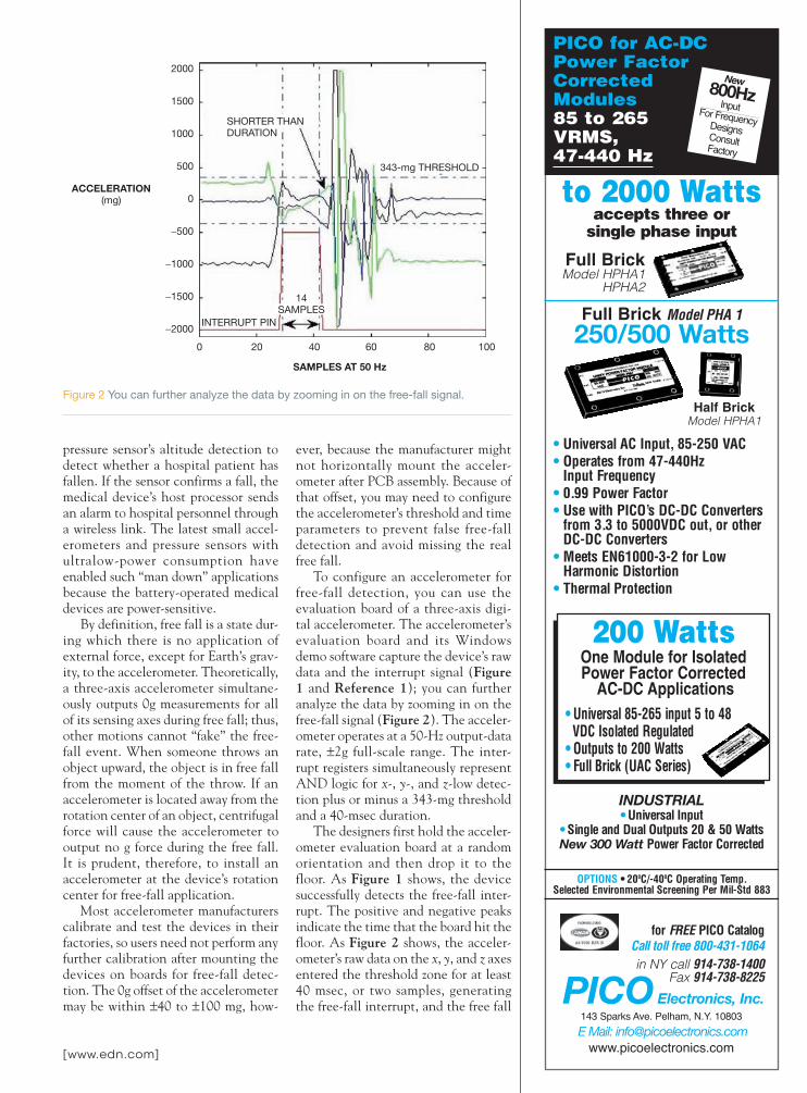
to 2000 Wattsaccepts three or
single phase input
Full BrickModel HPHA1
HPHA2
Full Brick Model PHA 1
250/500 Watts
Half BrickModel HPHA1
• Universal AC Input, 85-250 VAC• Operates from 47-440Hz
Input Frequency• 0.99 Power Factor• Use with PICO’s DC-DC Converters
from 3.3 to 5000VDC out, or other DC-DC Converters
• Meets EN61000-3-2 for Low Harmonic Distortion
• Thermal Protection
200 WattsOne Module for IsolatedPower Factor Corrected
AC-DC Applications• Universal 85-265 input 5 to 48
VDC Isolated Regulated• Outputs to 200 Watts• Full Brick (UAC Series)
INDUSTRIAL• Universal Input
• Single and Dual Outputs 20 & 50 WattsNew 300 Watt Power Factor Corrected
OPTIONS • 200C/-400C Operating Temp.Selected Environmental Screening Per Mil-Std 883
for FREE PICO CatalogCall toll free 800-431-1064in NY call 914-738-1400
Fax 914-738-8225PICOElectronics, Inc.143 Sparks Ave. Pelham, N.Y. 10803E Mail: [email protected]
www.picoelectronics.com
PICO for AC-DCPower FactorCorrectedModules85 to 265VRMS,47-440 Hz
New800HzInputFor FrequencyDesignsConsultFactory
pressure sensor’s altitude detection to detect whether a hospital patient has fallen. If the sensor confirms a fall, the medical device’s host processor sends an alarm to hospital personnel through a wireless link. The latest small accel-erometers and pressure sensors with ultralow-power consumption have enabled such “man down” applications because the battery-operated medical devices are power-sensitive.
By definition, free fall is a state dur-ing which there is no application of external force, except for Earth’s grav-ity, to the accelerometer. Theoretically, a three-axis accelerometer simultane-ously outputs 0g measurements for all of its sensing axes during free fall; thus, other motions cannot “fake” the free-fall event. When someone throws an object upward, the object is in free fall from the moment of the throw. If an accelerometer is located away from the rotation center of an object, centrifugal force will cause the accelerometer to output no g force during the free fall. It is prudent, therefore, to install an accelerometer at the device’s rotation center for free-fall application.
Most accelerometer manufacturers calibrate and test the devices in their factories, so users need not perform any further calibration after mounting the devices on boards for free-fall detec-tion. The 0g offset of the accelerometer may be within ±40 to ±100 mg, how-
ever, because the manufacturer might not horizontally mount the acceler-ometer after PCB assembly. Because of that offset, you may need to configure the accelerometer’s threshold and time parameters to prevent false free-fall detection and avoid missing the real free fall.
To configure an accelerometer for free-fall detection, you can use the evaluation board of a three-axis digi-tal accelerometer. The accelerometer’s evaluation board and its Windows demo software capture the device’s raw data and the interrupt signal (Figure 1 and Reference 1); you can further analyze the data by zooming in on the free-fall signal (Figure 2). The acceler-ometer operates at a 50-Hz output-data rate, ±2g full-scale range. The inter-rupt registers simultaneously represent AND logic for x-, y-, and z-low detec-tion plus or minus a 343-mg threshold and a 40-msec duration.
The designers first hold the acceler-ometer evaluation board at a random orientation and then drop it to the floor. As Figure 1 shows, the device successfully detects the free-fall inter-rupt. The positive and negative peaks indicate the time that the board hit the floor. As Figure 2 shows, the acceler-ometer’s raw data on the x, y, and z axes entered the threshold zone for at least 40 msec, or two samples, generating the free-fall interrupt, and the free fall
Figure 2 You can further analyze the data by zooming in on the free-fall signal.
ACCELERATION(mg)
SAMPLES AT 50 Hz
2000
1500
1000
500
0
−500
−1000
−1500
−2000
0
INTERRUPT PIN
20 40 60 80 100
SHORTER THAN DURATION
343-mg THRESHOLD
14SAMPLES
[ www.edn.com ]
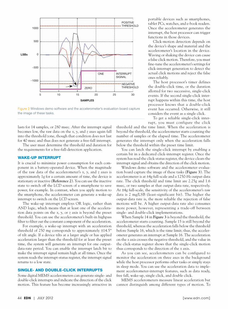
44 EDN | JuLY 2012 [ www.edn.com ]
lasts for 14 samples, or 280 msec. After the interrupt signal becomes low, the raw data on the x, y, and z axes again fall into the threshold zone, though that condition does not last for 40 msec and thus does not generate a free-fall interrupt.
The user must determine the threshold and duration for the requirements for a free-fall-detection application.
Wake-up interruptIt is crucial to minimize power consumption for each com-ponent in a battery-operated device. When the magnitude of the raw data of the accelerometer’s x, y, and z axes is approximately 1g for a certain amount of time, the device is stationary or inactive (Reference 2). You can use the inactive state to switch off the LCD screen of a smartphone to save power, for example. In contrast, when you apply motion to the smartphone, the accelerometer can generate a wake-up interrupt to switch on the LCD screen.
The wake-up interrupt employs OR logic, rather than AND logic, which means that at least one of the accelera-tion data points on the x, y, or z axis is beyond the preset threshold. You can use the accelerometer’s built-in highpass filter to filter out the constant component of the acceleration.
For example, a wake-up interrupt with an acceleration threshold of 250 mg corresponds to approximately ±14.5° of tilt angle. If a device tilts at a larger angle or has applied acceleration larger than the threshold for at least the preset time, the system will generate an interrupt for one output-data-rate period. You can enable the interrupt latch bit to make the interrupt signal remain high at all times. Once the system reads the interrupt-status register, the interrupt signal returns to a low state.
Single- and double-click interruptSSome digital MEMS accelerometers can generate single- and double-click interrupts and indicate the direction of the click motion. This feature has become increasingly attractive in
portable devices such as smartphones, tablet PCs, watches, and e-book readers. Once the accelerometer generates the interrupt, the host processor can trigger functions in those devices.
Click-motion detection depends on the device’s shape and material and the accelerometer’s location in the device. Waving or shaking the device can cause a false click motion. Therefore, you must fine-tune the accelerometer’s settings for click-interrupt generation to detect the actual click motions and reject the false ones reliably.
The host processor’s timer defines the double-click time, or the duration allotted for two successive, single-click events. If the second single-click inter-rupt happens within this time, the host processor knows that a double-click event has occurred. Otherwise, it still considers the event as a single click.
To get a reliable single-click inter-rupt, you must configure the click
threshold and the time limit. When the acceleration is beyond the threshold, the accelerometer starts counting the number of samples or the elapsed time. The accelerometer generates the interrupt only when the acceleration falls below the threshold within the preset time limit.
You can latch the single-click interrupt by enabling a certain bit in a dedicated click-interrupt register. Once the system has read the click-status register, the device clears the interrupt signal and obtains the direction of the click motion.
Windows demo software and the accelerometer evalua-tion board capture the image of these tasks (Figure 3). The accelerometer is at ±4g full-scale and a 1250-Hz output-data rate. The click threshold and time limit are 2.25g and 1.6 msec, or two samples at that output-data rate, respectively. At ±4g full-scale, the sensitivity of the accelerometer’s raw data is 2 mg/LSB (least-significant bit). The higher the output-data rate is, the more reliable the rejection of false motions will be. A higher output-data rate also consumes more power, however, representing a trade-off between single- and double-click implementations.
When Sample 14 in Figure 3 is beyond the threshold, the accelerometer starts counting. Sample 15 is still beyond the threshold, whereas the acceleration falls below the threshold before Sample 16, which is the time limit; thus, the acceler-ometer generates an interrupt at Sample 16. The acceleration on the x axis crosses the negative threshold, and the value in the click-status register shows that the single-click motion thus corresponds to the direction of the x axis.
As you can see, accelerometers can be configured to monitor the acceleration on three axes in the background while the host processor performs other tasks or simply stays in sleep mode. You can use the acceleration data to imple-ment accelerometer-interrupt features, such as data ready, free fall, wake-up, single click, and double click.
MEMS accelerometers measure linear acceleration but cannot distinguish among different types of motion. To
LSBs
SAMPLES
1000
500
0
−500
−1000
5 10 15 20 25 30
POSITIVE THRESHOLD
NEGATIVE THRESHOLD
ONE
ZERO
INTERRUPT SIGNAL
Figure 3 Windows demo software and the accelerometer’s evaluation board capture the image of these tasks.

implement reliable and robust inter-rupt-based applications, including screen rotation, position orientation, and single- and double-click detec-tion, the host processor must read and process the accelerometer’s raw data using the requirements of each application.
Future MEMS accelerometers will have more built-in advanced features and computing capabilities to generate those interrupts reliably and to offload data processing from the external host processor.EDN
AcknowledgmentThis article originally appeared on EDN’s sister site, Planet Analog, www.eetimes.com/4233325.
RefeRences 1 “STEVAL-MKI022V1: MEMS 3-axis ±2g/±4g/±8g smart digital output eval-uation board based on nano acceler-ometer LIS331DLH,” STMicroelectron-ics, http://bit.ly/KWZ58e. 2 “AN3182: Tilt measurement using a low-g 3-axis accelerometer,” STMicro-electronics, April 2010, http://bit.ly/JuxoEo.
AuthoRs’ b iogRAphiesJay Esfandyari is a MEMS-product-mar-keting engineer at STMicroelectronics. He is the author of many papers and articles on MEMS technologies, products, and ap-plications. Esfandyari holds master’s and doctorate degrees in electrical engineer-ing from the University of Technology of Vienna (Austria). You can reach him at [email protected].
Gang Xu, senior application engineer at STMicroelectronics, has more than 10 years of experience in the application of MEMS accelerometers, gyroscopes, and magnetometers. He received a doctorate in electrical engineering from Shanghai Jiao Tong University (Shanghai) in 1996.
Paolo Bendiscioli is an application manag-er for the motion-MEMS division of STMi-croelectronics and has more than 10 years of experience in the applications of MEMS accelerometers, gyroscopes, and magnetom-eters. He is responsible for the application-development and customer-technical-sup-port teams. Bendiscioli received a degree in electronics engineering from the University of Pavia (Italy) in 1997.
[ www.edn.com ]
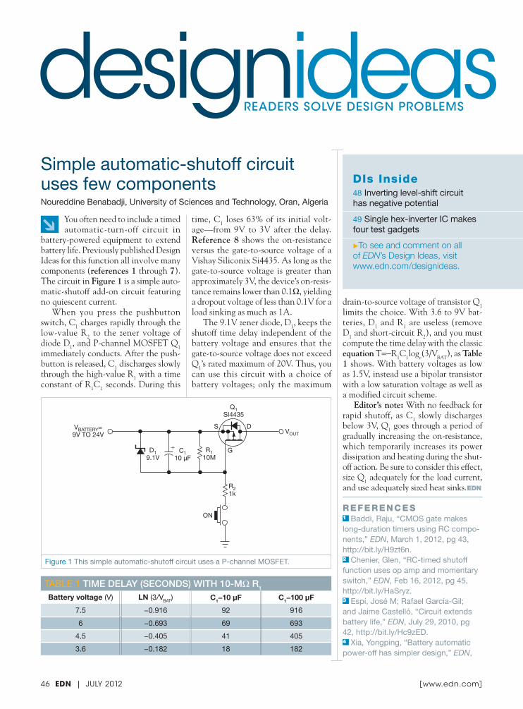
↘ You often need to include a timed automatic-turn-off circuit in
battery-powered equipment to extend battery life. Previously published Design Ideas for this function all involve many components (references 1 through 7). The circuit in Figure 1 is a simple auto-matic-shutoff add-on circuit featuring no quiescent current.
When you press the pushbutton switch, C1 charges rapidly through the low-value R2 to the zener voltage of diode D1, and P-channel MOSFET Q1 immediately conducts. After the push-button is released, C1 discharges slowly through the high-value R1 with a time constant of R1C1 seconds. During this
time, C1 loses 63% of its initial volt-age—from 9V to 3V after the delay. Reference 8 shows the on-resistance versus the gate-to-source voltage of a Vishay Siliconix Si4435. As long as the gate-to-source voltage is greater than approximately 3V, the device’s on-resis-tance remains lower than 0.1Ω, yielding a dropout voltage of less than 0.1V for a load sinking as much as 1A.
The 9.1V zener diode, D1, keeps the shutoff time delay independent of the battery voltage and ensures that the gate-to-source voltage does not exceed Q1’s rated maximum of 20V. Thus, you can use this circuit with a choice of battery voltages; only the maximum
drain-to-source voltage of transistor Q1limits the choice. With 3.6 to 9V bat-teries, D1 and R1 are useless (remove D1 and short-circuit R2), and you must compute the time delay with the classic equation T=−R1C1loge(3/VBAT), as Table 1 shows. With battery voltages as low as 1.5V, instead use a bipolar transistor with a low saturation voltage as well as a modified circuit scheme.
Editor’s note: With no feedback for rapid shutoff, as C1 slowly discharges below 3V, Q1 goes through a period of gradually increasing the on-resistance, which temporarily increases its power dissipation and heating during the shut-off action. Be sure to consider this effect, size Q1 adequately for the load current, and use adequately sized heat sinks.EDN
RefeRences1 Baddi, Raju, “CMOS gate makes long-duration timers using RC compo-nents,” EDN, March 1, 2012, pg 43, http://bit.ly/H9zt6n.2 Chenier, Glen, “RC-timed shutoff function uses op amp and momentary switch,” EDN, Feb 16, 2012, pg 45, http://bit.ly/HaSryz.3 Espí, José M; Rafael García-Gil; and Jaime Castelló, “Circuit extends battery life,” EDN, July 29, 2010, pg 42, http://bit.ly/Hc9zED.4 Xia, Yongping, “Battery automatic power-off has simpler design,” EDN,
Simple automatic-shutoff circuit uses few componentsNoureddine Benabadji, University of Sciences and Technology, Oran, Algeria
DIs Inside48 Inverting level-shift circuit has negative potential
49 Single hex-inverter IC makes four test gadgets
▶To see and comment on all of EDN’s Design Ideas, visit www.edn.com/designideas.
readerS SOLVe deSIGN PrOBLeMSdesignideas
46 EDN | JULY 2012 [ www.edn.com ]
EDN120510DI5293 Fig 1.eps DIANE
S D
Q1SI4435
R110M
R21k
C110 μF
D19.1V
G+
VOUT
ON
VBATTERY=9V TO 24V
Figure 1 This simple automatic-shutoff circuit uses a P-channel MOSFET.
TABlE 1 Time delay (SecondS) wiTh 10-mΩ R1
Battery voltage (V) LN (3/VBAT) C1=10 μF C1=100 μF
7.5 −0.916 92 916
6 −0.693 69 693
4.5 −0.405 41 405
3.6 −0.182 18 182

Hardware prototyping doesn’t have to be hard. With Maxim’s new design tools, you can quickly add analog and mixed-signal functions to your FPGA reference platform without having to solder a single pin. Snap on peripherals using a Pmod™ port. Or plug in a module to power it all. With the right tools, everything is easier.
Tools for FPGA Design• 15 Pmod-compatible peripheral modules are available-buy individually, or buy the
full collection for $89.95
° Bitstream allows use in any port without HDL recoding for plug-and-play ease
° Sample C code is included to give you a head start on customization
• Compact power modules provide all the rails you need to power your FPGA design
© 2012 Maxim Integrated Products, Inc. All rights reserved. Innovation Delivered, Maxim, and the Maxim logo are trademarks or registered trademarks of Maxim Integrated Products, Inc., in the United States and other jurisdictions throughout the world. Pmod is a trademark of Digilent, Inc. All other company names may be trade names or trademarks of their respective owners.
Get the tools you need today.www.maxim-ic.com/FPGA-Design
Plug-and-Play FPGA Design ToolsQuickly add power, signal chain, and other functions to your design
www.em.avnet.com/maxim
™DIRECTwww.maxim-ic.com/shop www.digikey.com/maxim www.mouser.com/maximic

March 31, 2005, pg 80, http://bit.ly/bLJNgb.5 Gimenez, Miguel, “Scheme provides automatic power-off for bat-teries,” EDN, May 13, 2004, pg 92,
http://bit.ly/aUdD3s.6 Xia, Yongping, “Timer automatically shuts off,” EDN, Aug 17, 2000, pg 128, http://bit.ly/GRefMO.7 Elias, Kamil, “Timer provides power-
off function,” EDN, May 22, 1997, http://bit.ly/MlbQxg.8 “Si4435BDY P-Channel 30-V (D-S) MOSFET,” Vishay Siliconix, May 4, 2009, http://bit.ly/HaWjiZ.
↘ Digital-system designs require you to consider many core volt-
ages. Memory operates at 1.8V, I2C and FPGA devices operate at 3.3V, micro-controllers operate at 5V, and charge-coupled-device image sensors operate at −9 to 8V. Clocks for each device must suit their operating voltages.
You can use the level-shift circuit in Figure 1 to adjust an input clock signal to the proper logic-high and logic-low voltage levels, including negative volt-ages. This property is handy for devices that need a negative voltage, such as a charge-coupled-device sensor. Although the circuit’s output clock is 180°-inverted relative to the input clock, that inversion does not affect the function of the device.
The level-shift circuit comprises
fast-switching transistors Q1 and Q2. The user chooses level-shift high and level-shift low, which are dc-bias voltag-es and which connect to the transistor emitters, to match the desired output high- and low-logic levels. C1, R1, D1, C2, R2, and D2 keep the base voltages of Q1 and Q2 close to that of their emitters.
Because memory and charge-cou-pled-device sensors usually have high-fre-quency clocks, you can choose C1 and C2 to prevent low-frequen-cy-noise pass-through. The circuit in Figure 1 uses a 20-MHz sig-nal for measurements (Table 1) and thus uses
a value of 100 pF for C1 and C2. When the input voltage’s clock is low, Q1 turns on and Q2 turns off, driving the output voltage’s clock to the level shift’s high potential. When the input voltage’s clock is high, Q1 turns off and Q2 turns on, driving the output voltage’s clock to the level shift’s low potential, even when that potential is negative relative to ground.
Because of the circuit’s high switch-ing speeds, keep component leads as short as possible to minimize induc-tance. This caveat is especially true for C3 through C6’s leads to their respective transistor emitters and to the ground plane or the output ground return.EDN
Inverting level-shift circuit has negative potentialChun-Fu Lin and Shir-Kuan Lin, National Chiao Tung University,Hsinchu, Taiwan; and Hui-Shun Huang, Jyi-Jinn Chang, and Tai-Shan Liao, National Applied Research Laboratories, Hsinchu, Taiwan
designideas
48 EDN | JULY 2012 [ www.edn.com ]
EDNDI5260 Fig 1.eps DIANE
Q1
Q2
R33
R43
R12.2k
R53
VOUTPUTCLOCKVINPUTCLOCK
MMBT3640
MMBT2369
C1100 pF100V
C31000 pF
50V
C40.1 μF50V
D1HSMS2805
C2100 pF100V
R22.2k
D2HSMS2805
C51000 pF
50V
C60.1 μF50V
LEVELSHIFTHIGH
LEVELSHIFTLOW
0V
Figure 1 This simple and fast level-shift circuit can adjust an input clock to both positive and negative voltage levels.
TABLE 1 Input and output clocksHigh/low level shift
(V)Input clock
(V)Output clock
(V)
3.3/0 0/5 3.3/0
20/10 0/5 20/10
−5/−10 0/5 −5/−10
2/−4 0/5 2/−4

↘ This Design Idea describes a simple way that you can use one
hex-inverter package of an unbuffered HD14069UB CMOS (Reference 1) to make four test gadgets: a logic probe with well-defined logic-voltage win-dows and with an input impedance of approximately 1 MΩ; a continuity tes-ter whose upper limiting resistance can be tens of ohms to tens of megohms; a single or train pulse injector or a modest signal generator; and a high-impedance audio probe. You can assemble these gadgets using the six inverter gates of a 4069, two or three transistors, and a few passive components.
In a two-gate CMOS/TTL-com-patible probe, the resistor network comprising R1 through R4 biases the inverter’s inputs (Figure 1). Because of the gates’ high input impedance, R1through R4 can have values of approxi-mately 100 kΩ to 1 MΩ. The probe’s source/sink current is small at the probe tip because of the high resistances of R1 through R4; as a result, the probe tip essentially does not affect the logic-voltage level at the test point. Knowing
the gates’ input threshold voltage, you can calculate the required values of resistors R1 through R4.
The upper gate detects logic zero, and the lower gate detects logic one. Set an upper limit to the logic-zero voltage and calculate the values of R1 and R2. Arbitrarily select R1=1 MΩ and seek a value for R2 such that the voltage at the input of the upper gate is just the threshold voltage. Thus, R2=R1(VT−VL)/(VS−VT), where VT is the threshold volt-age, VL is the logic-zero voltage, and VSis the supply voltage. Similarly, set a lower limit on the logic-one voltage VTand seek a value for R4 in terms of R3. By appropriately selecting R3, keeping in mind the quiescent biasing of the gates to keep both the LEDs off in the probe’s suspended condition, you can obtain the value of R4: R4=R3VT/(VH−VT).
The following equation calcu-lates the probe current: IP=[−(V−VI)(R3+R4)+VI(R1+R2)]/(R1+R2)(R3+R4), where IP is the probe current and VI is the probe-tip voltage. It thus follows that the probe impedance for any voltage at the probe tip is greater than 1 MΩ. For
packages of 4069 that exhibit a larger threshold voltage, such as 3V, you can help reduce it by including a diode fol-lowed by a 10-kΩ load resistor to ground in the positive supply rail to the chip.
Developers often use continuity testers (Figure 2 and Reference 2) as elementary test gadgets; such testers are indispensable on a work bench. One of the 4069’s gates, with its high input impedance and with a threshold voltage for the transition of the output of the gate, allows you to build the continuity tester with an upper limit on the resis-tance of the test circuit. The total of the resistance between the probes and the resistance in the switching arrangement forms a voltage-divider network, produc-ing a voltage at the input of the gate. When the two resistances are equal, the voltage at the gate input is half the supply voltage. The transition threshold voltage of the gate is also nearly half the supply voltage; therefore, the selected resistor in the switching branch sets the approxi-mate threshold-continuity resistance.
A useful alternative arrangement is to have a variable resistor in place of the switchable resistors. This approach allows you to set the threshold-continu-ity resistance arbitrarily by adjusting this resistor after including the desired resis-tance between the probe tips and observ-ing the LED’s glow. The variable resistor
Single hex-inverter IC makes four test gadgetsRaju Baddi, Tata Institute of Fundamental Research, Pune, India
EDN120621DI5295 Fig 1.eps DIANE
470
R1
R2
470R3
R4
+
Figure 1 You can make a logic probe TTL/CMOS-compatible using just two gates from a single unit of an HD14069UB hex inverter. The suggested values for threshold and supply voltages are 2.5 and 5V, respectively; those for R1, R2, R3, and R4 are 1 MΩ, 680 kΩ, 200 kΩ, and 1 MΩ, respectively.
EDN120621DI5295 Fig 2.eps DIANE
470
1k
2k
4.7k
6.8k
10k
10M
1M
100k
56k
20k
+
1 TO 2k
Figure 2 This single-gate continuity tester has an adjustable detection threshold.
JULY 2012 | EDN 49[ www.edn.com ]
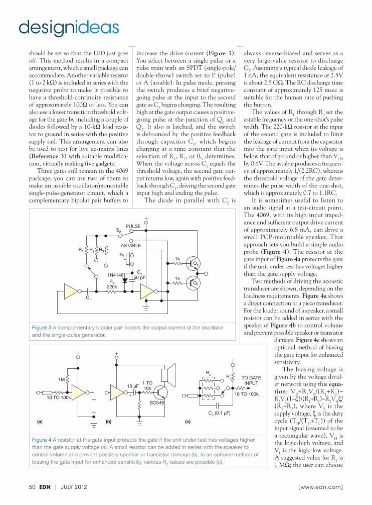
should be set so that the LED just goes off. This method results in a compact arrangement, which a small package can accommodate. Another variable resistor (1 to 2 kΩ) is included in series with the negative probe to make it possible to have a threshold-continuity resistance of approximately 100Ω or less. You can also use a lower transition threshold volt-age for the gate by including a couple of diodes followed by a 10-kΩ load resis-tor to ground in series with the positive supply rail. This arrangement can also be used to test for live ac-mains lines (Reference 3) with suitable modifica-tion, virtually making five gadgets.
Three gates still remain in the 4069 package; you can use two of them to make an astable oscillator/monostable single-pulse-generator circuit, which a complementary bipolar pair buffers to
increase the drive current (Figure 3). You select between a single pulse or a pulse train with an SPDT (single-pole/double-throw) switch set to P (pulse) or A (astable). In pulse mode, pressing the switch produces a brief negative-going pulse at the input to the second gate as C2 begins charging. The resulting high at the gate output causes a positive-going pulse at the junction of Q1 and Q2. It also is latched, and the switch is debounced by the positive feedback through capacitor C1, which begins charging at a time constant that the selection of R1, R2, or R3 determines. When the voltage across C1 equals the threshold voltage, the second gate out-put returns low, again with positive feed-back through C1, driving the second gate input high and ending the pulse.
The diode in parallel with C2 is
always reverse-biased and serves as a very large-value resistor to discharge C2. Assuming a typical diode leakage of 1 nA, the equivalent resistance at 2.5V is about 2.5 GΩ. The RC discharge time constant of approximately 125 msec is suitable for the human rate of pushing the button.
The values of R1 through R3 set the astable frequency or the one-shot’s pulse width. The 220-kΩ resistor at the input of the second gate is included to limit the leakage of current from the capacitor into the gate input when its voltage is below that of ground or higher than VDDby 0.6V. The astable produces a frequen-cy of approximately 1/(2.2RC), whereas the threshold voltage of the gate deter-mines the pulse width of the one-shot, which is approximately 0.7 to 1.1RC.
It is sometimes useful to listen to an audio signal at a test-circuit point. The 4069, with its high input imped-ance and sufficient output drive current of approximately 6.8 mA, can drive a small PCB-mountable speaker. That approach lets you build a simple audio probe (Figure 4). The resistor at the gate input of Figure 4a protects the gate if the unit under test has voltages higher than the gate supply voltage.
Two methods of driving the acoustic transducer are shown, depending on the loudness requirements. Figure 4a shows a direct connection to a piezo transducer. For the louder sound of a speaker, a small resistor can be added in series with the speaker of Figure 4b to control volume and prevent possible speaker or transistor
damage. Figure 4c shows an optional method of biasing the gate input for enhanced sensitivity.
The biasing voltage is given by the voltage divid-er network using this equa-tion: VB=R2VS/(R1+R2)−R2VL(1−ξ)/(R1+R2)−R2VHξ/(R1+R2), where VS is the supply voltage, ξ is the duty cycle (TH/(TH+TL)) of the input signal (assumed to be a rectangular wave), VH is the logic-high voltage, and VL is the logic-low voltage. A suggested value for R1 is 1 MΩ; the user can choose
EDN120621DI5295 Fig 3.eps DIANE
R4220k
R1 R2 R3
C1
S1
S2
C250 pF
Q1
ASTABLE
1k
Q2
1k
PULSE
+
1N4148
EDN120621DI5295 Fig 4.eps DIANE
1M
+
10 TO 100k
(a)
+
+
(b)
BC549
1 TO10k10 µF
+
CC (0.1 µF)
10 TO 100k
TO GATEINPUT
R1
R2
(c)
Figure 3 A complementary bipolar pair boosts the output current of the oscillator and the single-pulse generator.
Figure 4 A resistor at the gate input protects the gate if the unit under test has voltages higher than the gate supply voltage (a). A small resistor can be added in series with the speaker to control volume and prevent possible speaker or transistor damage (b). In an optional method of biasing the gate input for enhanced sensitivity, various R2 values are possible (c).
designideas
50 EDN | JULY 2012 [ www.edn.com ]
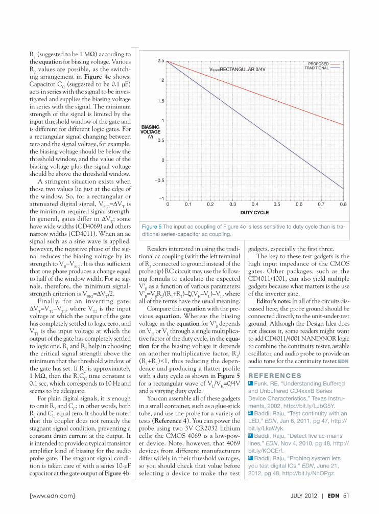
JULY 2012 | EDN 51[ www.edn.com ]
R2 (suggested to be 1 MΩ) according to the equation for biasing voltage. Various R2 values are possible, as the switch-ing arrangement in Figure 4c shows. Capacitor CC (suggested to be 0.1 μF) acts in series with the signal to be inves-tigated and supplies the biasing voltage in series with the signal. The minimum strength of the signal is limited by the input threshold window of the gate and is different for different logic gates. For a rectangular signal changing between zero and the signal voltage, for example, the biasing voltage should be below the threshold window, and the value of the biasing voltage plus the signal voltage should be above the threshold window.
A stringent situation exists when those two values lie just at the edge of the window. So, for a rectangular or attenuated digital signal, VSIG=ΔVT is the minimum required signal strength. In general, gates differ in ΔVT; some have wide widths (CD4069) and others narrow widths (CD4011). When an ac signal such as a sine wave is applied, however, the negative phase of the sig-nal reduces the biasing voltage by its strength to VB−VSIG. It is thus sufficient that one phase produces a change equal to half of the window width. For ac sig-nals, therefore, the minimum signal-strength criterion is VSIG=ΔVT/2.
Finally, for an inverting gate, ΔVT=VT2–VT1, where VT2 is the input voltage at which the output of the gate has completely settled to logic zero, and VT1 is the input voltage at which the output of the gate has completely settled to logic one. R1 and R2 help in choosing the critical signal strength above the minimum that the threshold window of the gate has set. If R2 is approximately 1 MΩ, then the R2CC time constant is 0.1 sec, which corresponds to 10 Hz and seems to be adequate.
For plain digital signals, it is enough to omit R2 and CC; in other words, both R2 and CC equal zero. It should be noted that this coupler does not remedy the stagnant signal condition, preventing a constant drain current at the output. It is intended to provide a typical transistor amplifier kind of biasing for the audio probe gate. The stagnant signal condi-tion is taken care of with a series 10-µF capacitor at the gate output of Figure 4b.
Readers interested in using the tradi-tional ac coupling (with the left terminal of R2 connected to ground instead of the probe tip) RC circuit may use the follow-ing formula to calculate the expected V'B as a function of various parameters: V'B=VSR2/(R1+R2)–ξ(VH–VL)–VL, where all of the terms have the usual meaning.
Compare this equation with the pre-vious equation. Whereas the biasing voltage in the equation for V'B depends on VH or VL through a single multiplica-tive factor of the duty cycle, in the equa-tion for the biasing voltage it depends on another multiplicative factor, R2/(R1+R2)<1, thus reducing the depen-dence and producing a flatter profile with a duty cycle as shown in Figure 5 for a rectangular wave of VL/VH=0/4V and a varying duty cycle.
You can assemble all of these gadgets in a small container, such as a glue-stick tube, and use the probe for a variety of tests (Reference 4). You can power the probe using two 3V CR2032 lithium cells; the CMOS 4069 is a low-pow-er device. Note, however, that 4069 devices from different manufacturers differ widely in their threshold voltages, so you should check that value before selecting a device to make the test
gadgets, especially the first three. The key to these test gadgets is the
high input impedance of the CMOS gates. Other packages, such as the CD4011/4001, can also yield multiple gadgets because what matters is the use of the inverter gate.
Editor’s note: In all of the circuits dis-cussed here, the probe ground should be connected directly to the unit-under-test ground. Although the Design Idea does not discuss it, some readers might want to add CD4011/4001 NAND/NOR logic to combine the continuity tester, astable oscillator, and audio probe to provide an audio tone for the continuity tester.EDN
RefeRences1 Funk, RE, “Understanding Buffered and Unbuffered CD4xxxB Series Device Characteristics,” Texas Instru-ments, 2002, http://bit.ly/LJbG5Y.2 Baddi, Raju, “Test continuity with an LED,” EDN, Jan 6, 2011, pg 47, http://bit.ly/LkaWyk. 3 Baddi, Raju, “Detect live ac-mains lines,” EDN, Nov 4, 2010, pg 48, http://bit.ly/KOCErf.4 Baddi, Raju, “Probing system lets you test digital ICs,” EDN, June 21, 2012, pg 48, http://bit.ly/NhOPgz.
BIASINGVOLTAGE
(V)
DUTY CYCLE
VSIG=RECTANGULAR 0/4VPROPOSED
TRADITIONAL
2
1.5
1
0.5
0
–0.5
–10 0.1 0.2 0.3 0.4 0.5 0.6 0.7 0.8
2.5
Figure 5 The input ac coupling of Figure 4c is less sensitive to duty cycle than is tra-ditional series-capacitor ac coupling.

T he US government is expected in Septem-ber to start issuing reg-
ulations to carry out the anti-counterfeiting provision in the 2012 National Defense Autho-rization Act. A Senate Armed Services Committee investi-gation that found more than 1,800 instances of counterfeit electronics in the DOD (Depart-ment of Defense) supply chain prompted the provision.
Under the provision’s terms, contractors can’t charge the DOD for remediating problems related to counterfeit parts. The DOD and its contractors must buy electronic components from OCMs (original-component manufacturers), their autho-rized distributors, or “trusted suppliers” wherever possible, and contractors must establish policies to “eliminate” counter-
feit electronic parts from the supply chain.
Henry Livingston, an engi-neering fellow and techni-cal director at BAE Systems and one of the speakers at a recent symposium on counter-feit electronics, identified several aspects of the provision that will likely prove challenging. The term “eliminate,” for example, is definitive but might be difficult to achieve in practice, he said.
The provision is unclear regarding responsibility for remedial costs. It doesn’t define what a remedy is or how much responsibility a company must assume for costs. The provision does not focus on where the component enters the supply chain, and it lacks requirements for independent distributors or OCMs to help support the iden-tification of counterfeits.
Nothing in the provision addresses what contractors are supposed to do with coun-terfeits they discover. The logi-cal decision would be to return them for a refund, but counter-feit parts should not be put back into the supply chain, where they can then be sold to others.
The government was ex- pected to define several terms and offer guidance on how sup-pliers should report counterfeits. As of June 27, however, there had been no word. By the end of September, the DOD is sup-posed to propose regulations that outline specific contractor responsibilities. Without those details, companies can’t accu-rately assess how well they’ll be able to meet the require-ments.—by Tam HarbertThis story was originally posted by EBN: http://bit.ly/P3OAaw.
G R E E N U P D AT E
000
109
8
7 65
43
2
1
MEDICAL TO fALL UNDEr rOHS SCOpE IN 2014If you think rOHS is in your rearview mirror, think again. A significant electronics market is going to feel the impact of the rOHS directive within the next few years and maybe caught unprepared.
Medical devices will fall under the scope of the rOHS directive starting in 2014, according to Gary Nevison of Newark/Element14. Medical devices have so far been exempt from rOHS because of the critical nature of the devices and the necessary use of hazardous materials, such as lead, to protect users from radiation. The sale of noncompliant devices into the European Union won’t be halted until 2019.
The manufacture of medical devices is still
a very tightly held business. It is highly regu-lated, and it is difficult to quality for the various approvals required by law. Medical-electronics companies have also been slow to outsource manufacturing, preferring to retain quality control in-house. Now that medical devices will fall under rOHS, that sector will likely ex-perience many of the same issues the broader industry has encountered in interpreting and implementing the directive’s requirements.
Medical equipment companies can continue to ask for exemptions to the rule.—by Barbara Jorgensen, EBN community editorThis story was originally posted by EBN:http://bit.ly/LWb11u.
supplychainLinking design and resources
Questions linger on anti-counterfeit rules
[www.edn.com]52 EDN | JuLY 2012
OUTLOOK
CONTrACT MANUfACTUrErS CApITALIzE ON SHIfT TO ULTrABOOkS With their main businessin notebook pCs under pressure, ODMs (original-design manufacturers) are adding new capabilities that will allow them to capitalize on the soaring sales of ultrabooks, according to research firm IHS.
“ODMs now are hoping to jump in on the action on ultrabooks, predicted to be the next big growth sector in computing, by securing the casings for anticipated future ultrabook orders,” says Thomas J Dinges, CfA, senior principal analyst for EMS and ODM research at IHS.
Casing companies sell metal cases that serve as the frames of electronic devices. To date, Taiwan-based Compal Electronics Inc has invested tens of millions of dollars in joint ventures with casing suppliers in China to support the needs of its notebook customers. Overall, the major notebook ODMs will attempt to pro-cure up to 10,000 machines in 2012 for their casing-manufacturing operations and joint ventures.
With the production of ultrabooks expected to ramp up and Apple’s sales continuing to grow, casing supplies will remain tight for the near term, IHS believes.
—by Amy Norcross

Flexibility.You think about innovation, we think about the rest.
Our team of engineers has the right mix of technical skills and application experience to give you the support you need – throughout the design chain. Extensive technical support, FPGA design, and world-class training. That’s what the No. 1 in design support can do to help you focus on what you do best and successfully compete in the global market. Our solutions bend to meet your needs.
What can we do for you? www.avnetexpress.com
Design Chain sOlUtiOns FROM aVnet
accelerating your success!™1 800 332 8638 | www.avnetexpress.com | @avnetdesignwire

Components and paCkaging
Vishay panel potentiometer targets low-profile, low-weight equipment
↘ The Sfernice P16S potentiometer features a unique knob driving that incor-porates a cermet or conductive-plastic potentiometer. Mounting hardware
and terminals are placed on the panel’s back side, providing for a minimum clear-ance and use in small, low-profile, low-weight equipment. The power rating is 1W at 40°C. TCR is ±150 ppm/°C typical, and dielectric strength is 2.5 kVRMS. The P16S is available in a 7-mm bushing length with a 16-mm knob diameter and a temperature range of −40 to +125°C. Samples are available now, as are production quantities, with lead times of eight to 10 weeks for larger orders. Pricing starts at $6 per piece (1000) for US delivery.Vishay Intertechnology, www.vishay.com
↘ The ASRM2 mini antisurge axial-leaded resistor has a voltage
rating of 4 kV, with an overload voltage rating of 5 kV, and is rated for 2W of continuous power. The ASR series is designed to handle high-voltage pulses of up to 10 kV, depending on size and resis-tance value, for thousands of pulse events. The ASR has a flameproof coat-ing per UL94 V-0 and is ROHS-
compliant. The ASR/ASRM is designed as a suitable surge resistor for many power supplies, CRTs and other display types, small motor controls, security systems, industrial automation and con-trol, snubbers, power-supply primary-side discharge
productroundupresistors, and LED lighting. The series is suited for high-voltage applications, including medical devices, plasma cut-ters, welding equipment, personal-protec-tion devices, power- and phone-distribu-tion protection, and instrumentation. Pricing varies with size and resistance value, ranging from 5 cents to 12 cents each in full-reel quantities.Stackpole Electronics, www.seielect.com
NXP MOSFETs have tin-plated, solderable side pads
↘ The PMPB11EN and PMPB20EN 30V N-channel MOSFETs are
housed in a 2×2-mm low-profile DFN (discrete flat no-lead) package with tin-plated, solderable side pads. The side pads offer optical soldering inspection and a better quality of sol-der connection compared with convention-al leadless pack-ages. The MOS-FETs are the first of more than 20 devices housed in the DFN-2020MD-6 (SOT1220) package. Both devices have a maximum drain current of >10A and very low drain-to-source on-resistance values of 12 mΩ typical and 16.5 mΩ typical at 10V for reduced conduction losses, enabling lower power consumption and longer battery life. Measuring 0.6 mm in height, the DFN2020 MOSFETs are thinner than most 2×2-mm products and thus are
suited for ultra-small load switch-es, power converters, and charger switches in portable applica-
tions such as smartphones and tablets. Eight times smaller than standard SO8 packages, the DFN2020 offers compara-
ble thermal resistance and can
54 EDN | JuLY 2012 [ www.edn.com ]
Stackpole axial-leaded resistor features 2W power rating
NIC Components Corp.
NIC’s Has Enhanced its Performance Passive Lineup
Having what You NeedFor Your Future
Designs & Applications
Visit NICcomp.com to search NIC’s Entire Offering!
Hybrid Electrolytic CapacitorsLowESR Capacitors
Long Life, High Voltage Capacitors
RF Ceramic CapacitorsSMT Film Capacitors
Thin Film ResistorsCurrent Sensing Resistors
SMT Circuit Protection
Power InductorsRF Chip InductorsEMI Suppression
NIC Components Focuses on thePerformance
Passives You Will Need...
30303030Years of Service
QuickBUILDER
DesignKITS
Search, Cross, & Design With
View Parts by Reference Design With
[ www.edn.com ]
replace many larger MOSFET packages with the same drain-to-source-on-resis-tance-value range. Pricing starts at 20 cents (10,000) for the PMPB11EN and 16 cents (10,000) for the PMPB20EN.NXP Semiconductors, www.nxp.com
Cellergy CLC supercapacitors offer small footprint
↘ The CLC series of supercapaci-tors offers low leakage current
with its small-footprint (12×12.5-mm) product. Heights range from 2.4 to 3.6 mm. The maximum leakage current is 1.5 μA for single-cell and 3 μA for dou-
ble-cell con-f i gu ra t ions . Used with bat-teries to deliv-er energy to the load, the supercapaci-t o r s t a r g e t such applica-
tions as RFID tags, wireless alarms, medical systems, low-power transmit-ters, and remote controls. They are offered with 3.5, 4.2, and 5.5V nominal voltages; ESR values from 300 to 720 mΩ; and capacitance values from 10 to 25 mF. The price for the 12×12.5-mm-packaged devices is $1.70 (5000). Standard lead time is four to six weeks; availability is expected by July 30.Cellergy, www.cellergycap.com
Fairchild P-Channel MOSFETs minimize board space in mobile devices
↘ The FDZ661PZ and FDZ663P P-channel, 1.5V-specif ied
PowerTrench 0.8×0.8-mm WL-CSP MOSFETs feature state-of-the-art fine pitch and minimize board space and drain-to-source on-resistance for a min-iature form factor. Packaging occupies 0.64 mm2 of PCB area, less than 16% of the area of a 2×2-mm CSP. The ultralow profile has a height of less than 0.4 mm when mounted to the PCB. The devic-es are suitable for use in battery-manage-ment and load-switch functions in mobile applications. The ROHS-compliant MOSFETs offer a gate-to-source voltage as low as −1.5V. They are priced at 26 cents (1000). Fairchild Semiconductor,www.fairchildsemi.com
Littelfuse Micro3 blade fuses address tight spaces
↘ The Micro3 line of blade fuses combines two individual fused
circuits into a single subminiature body.
Company Page
Advanced Power Electronics Corp USA 56
Agilent Technologies 17, C-3
AKM Semiconductor Inc 19
Analog Devices 15
Avnet 53
Caplugs 26
Carlton-Bates 35
Coilcraft 4
Digi-Key Corp C-1, C-2
Emulation Technology 9
Epcos 21
Hapro Inc 57
Interconnect Systems Inc 29
Company Page
International Rectifier 25
Ironwood Electronics 57
Lattice Semiconductor 3
Linear Technology 42A–42B, C-4
LPKF 31
Maxim Integrated Products 47
Mouser Electronics 6
National Instruments 13
NIC Components Corp 55
Pico Electronics Inc 7, 43
RF Monolithics Inc 45
Stanford Research Systems 37, 39, 41
Summit Microelectronics 11
UBM EDN 19, 40, 57
EDN provides this index as an additional service. The publisher assumes no liability for errors or omissions.
ADvERT ISER INDEx

Less than 15-mm wide, the fuses offer the same 5-mm terminal spacing and electrical perfor-mance as single-fuse solutions. Each fuse is rated for high temperature (under hood) oper-
ation, with an operating tempera-ture range from −40 to more than +125°C. The fuses also offer tighter overload tolerances and are available in four current rat-
ings from 5 to 15A, with a 32V-dc rating and standard 2.8-mm terminals. The products allow for more circuits in a small space, decreasing harness weight and maximizing area. Pricing depends on volume; the devices are in production now.Littelfuse, www.littelfuse.com
AVX TCJ high-voltage capacitors maintain 20% recommended voltage derating
↘ The TCJ series SMDs (surface-mount devices) are the industry’s first 63 and 75V single-anode tantalum polymer
capacitors, according to the vendor. The capacitors deliver high
capacitance, high voltage, and low ESR values in a small case size. Available in 1-μF/63V, 4.7-μF/63V, 10-μF/63V, 4.7-μF/75V, and 6.8-μF/75V rated voltages, they maintain 20% recom-mended voltage derat-ing, extending the usable voltage range. The TCJ series capac-itors maintain high reliability, exceeding 1% per 1000 hours at 85°C and full-rated voltage. They are suit-ed for high-voltage applications, including ac/dc converters supplying circuits in LCD TVs, base stations, rectifiers, switching hubs, and router and line filters, as well as LED power drivers in PC monitors and LED TVs. The TCJ series is free of piezo issues related to the use of MLCC ceramic capacitors in circuits such as backlight con-trollers in LCD monitors and displays. The high-voltage tanta-lum capacitors also reduce the number of parts required because of their lower ESR, increasing layout flexibility. Lead time for the series is 10 weeks. Contact the company for prices.AVX Corp, www.avx.com
Temp-Flex microwave coaxial cables provide fast signal speed
↘ Microwave coaxial cables designed for high-band-width applications are available with a solid-core
fluoropolymer-resin dielectric (low loss) or air-enhanced design with a fluoropolymer-resin layer applied over dual monofilaments (ultralow loss) around the center conduc-tor for increased signal speed. The cables provide phase stability, impedance tolerance of 50 to ±1Ω, tight time-delay tolerance, an FEP alternative to PTFE and ePTFE, bandwidth potential to 110 GHz, and stability under dynamic conditions. All cable sizes have a helically wrapped, silver-plated copper and flat-wire shield and braid to achieve superior shielding effectiveness. Standard solid-core construction coaxial cable delivers 70% VOP (velocity of propagation); the air-enhanced design achieves 85% to 88% VOP and improved insertion loss at high frequencies. The standard-product family comes in 047, 086, and 141 sizes; prices are based on volume with a six-week lead time.Temp-Flex LLC, www.tempflex.com
productroundup
56 EDN | JuLY 2012 [ www.edn.com ]
July 2012 | EDN 57
HAPRO ElectronicsTel: +1-516-794-40 80 · www.hameg.us
1GHz /3 GHz Spectrum AnalyzerHMS1000 | HMS1010 | HMS3000 | HMS3010 with Tracking Generator
from
$ 3,765
¸̧RoHS
product martThis advertising is for new and current products.
[ www.edn.com ]
Vishay VJ MLCCs feature Q factor of 2000
↘ The VJ HIFREQ series of high-frequency RF and microwave
surface-mount MLCCs features high self-resonance; a high Q factor, of 2000; and a low dissipation factor, of <0.05%. The devices are optimized for filter and matching networks and for amplifier and dc blocking circuits. They are offered in 0402, 0603, and 0805 case sizes with working voltages from 25 to 250V dc. The capacitors have wide capacitance ranges, from 1 pF to 1.5 nF, and tight tolerances, to ±0.1 pF; an aging rate of 0% per decade; and an operating tem-perature range of −55 to +125°C. Pricing starts at 6 cents per unit.Vishay Intertechnology,www.vishay.com
Reprints can be used in:
• Trade Show Handouts
• Media Kits
• Point-of-Purchase Displays
• Direct Mail Campaigns
Create a powerful statement for your product, service or companythrough professionally designed marketing materials utilizing editorialcontent from EDN.
Contact Wright’s Media to discuss how we can customize these materials to enhance your current marketing campaign.
U.S. copyright laws protect against unauthorized use of published content.
Call today
877- 652-5295
and allow our
reprint coordinator
to assist you with
some proven
marketing ideas.
REPRINTSEPRINTSPLAQUESPOSTERS
Customize Your Reprints!
82389_EDN_halfhoriz:Layout 1 10/26/11 12:13 PM Page 1

Ta l e s f r o m T h e C u b e
[ www.edn.com ]58 EDN | JuLY 2012
I didn’t find anything wrong with the logic, but I did find a lot of poor design practices, such as marginal tim-ing, asynchronous logic, poor ground-ing, and missing signal terminations. I rewired the board, added termination resistors, strengthened ground connec-tions, and even made changes to the FPGA by opening the internal routing files and manually rerouting signals and changing logic. The board passed all tests; the next step was to redesign it.
I discovered that the DSP manufac-turer no longer supported the product and that the DRAMs were obsolete. I
suggested redesigning with newer com-ponents, and everyone agreed, even though the software engineers would need to rewrite their low-level code.
After a month redesigning the board and a month for manufacture and assembly, the new board arrived. I asked the software engineers for their new code. They said they hadn’t had time to rewrite any code because the venture backers had insisted on a completed demo by a certain date; otherwise, the backers would pull the funding. The company’s CEO told me to redesign the hardware, putting back the obsolete
bob Zeidman • Zeidman ConsulTing
Da
nie
l Va
sc
on
ce
llo
s
This one really takes the cake— and the schematics
Early in my consulting career, a start-up company con-tacted me. It had designed a system for capturing medi-cal images and sending them over a network. The prod-uct was behind schedule, so the venture-capital backers had fired the founder, and the hardware engineers had quit in solidarity. The company was left with a bunch
of software engineers and hardware that didn’t work; my job was to fix it. There was no documentation, and the original engineer had taken the schematics home and refused to return them. I had to reverse-engineer a PCB and an FPGA by observing the external signals with an oscilloscope and a logic analyzer.
components so that the current software would still run. I reluctantly complied.
By this time, the original design engineer had made friends again with management and told them my design wouldn’t work. The CEO summoned me to his office, seeking reassurance. I had worked on this design so intently, reverse-engineering it without docu-mentation, testing it, and redesigning it twice, that I gave him a guarantee: If the board didn’t work, he wouldn’t have to pay me. I added, though, that the board would have a half-dozen blue wires to correct minor problems.
The board came back on a Friday afternoon, and I started running tests. Around 8 pm, my memory tests started failing intermittently, even though all of the signals looked correct. In the DSP’s data book, I read about the built-in DRAM controller. I was using the RAS-before-CAS (row-address strobe before column-address strobe) refresh mode of the memory, but I couldn’t find that mode in the data book. It eventually sank in that the developers of this pro-cessor had designed it before that mode existed, so data just disappeared slowly.
With the company’s future and my reputation on the line, I poured myself some coffee and let ideas float around in my head until a useful one surfaced. The processor was much slower than the rest of the board’s circuitry. I had designed PAL (programmable array logic) chips into the board at several locations. I real-ized I could actually reroute the RAS and CAS signals from the DSP through the PALs, implement a state machine to create new RAS and CAS signals to the DRAM, and assert them periodically to refresh it. The DSP clock was so slow and the PALs so fast that I could slip in a refresh between normal accesses.
The reworked board consistently passed the memory tests. On Monday, I presented it to the CEO and told him I’d been wrong: “I said the board would work with a half-dozen blue wires, but I needed only four.”EDN
Bob Zeidman is president and founder of both Zeidman Consulting and Software Analysis and Forensic Engineering Corp, both in Cupertino, CA.

Get a FREE 8 GB USB drive loaded with
power product resources*
www.agilent.com/find/N6700Power
Agilent N6700 Modular Power System
• 4 mainframes–manufacturing or R&D
• 34 modules from 20 to 500 WW
• 4 performance levels–basic to precision
No matter your application, accelerate with Agilent.
Whether it’s automotive ECU, military communications, base station power amplifi ers or general purpose test, maximize manufacturing throughput and R&D productivity. With seven new high-power modules from 300 to 500 W, Agilent helps you execute a wide range of high-power setups with the performance to measure milliamps accurately, too.
Power your most demanding setups with ease.
To view application videos scan QR code
or visit http://goo.gl/sgwbK
© Agilent Technologies, Inc. 2012. *While supplies last. Terms and conditions apply. u.s. 1-800-829-4444 canada: 1-877-894-4414

VIN VOUT
12VIN to 3.3VOUT EfficiencyIN OUT Efficiency100
90
80
70
60
50
400.50 1.00 1.50 2.00 2.50
Load Current (A)
Effic
ienc
y (%
)
FSW = 700kHz
LT8610-3.3
42V, 2MHz Sync Buck
Info & Free Samples
The LT®8610/11 are our first constant frequency, ultralow quiescent current high voltage monolithic synchronous buck regulators. They consume only 2.5µA of quiescent current while regulating an output of 3.3V from a 12V input source. Their low ripple Burst Mode® operation maintains high efficiencies at low output currents while keeping output ripple below 10mVP-P. Even at >2MHz switching frequency, high step-down ratios enable compact footprints for a wide array of applications, including automotive. The LT8611 enables accurate current regulation and monitoring for driving LEDs, charging batteries or supercaps, and for controlling power dissipation during fault conditions.
www.linear.com/product/LT8610
1-800-4-LINEAR
LT8610 Demo Circuit
Features
• 3.4V to 42V Input Range
• 2.5µA IQ Regulating @ 12VIN to 3.3VOUT
• Output Ripple <10mVP–P
• 99.9% Duty Cycle for Low Dropout
• 94% Efficiency at 1A, 12VIN to 3.3VOUT
• >2MHz Operation even with High Step-down Ratios
• Accurate Input/Output Current Regulation, Limiting and Monitoring (LT8611)
2.5A Output Current, 2.5µA IQ, 94% Efficient
, LT, LTC, LTM, Linear Technology, the Linear logo and Burst Mode are registered trademarks of Linear Technology Corporation. All other trademarks are the property of their respective owners.
http://video.linear.com/114
Actual Size15mm x 18mm


