Tutorial information about Prof. Jih-Sheng (Jason) Lai - International
57
JSL 1 High-Efficiency Power Conversion for Renewable Energy and Distribution Generation Professor Jih-Sheng (Jason) Lai Future Energy Electronics Center Virginia Polytechnic Institute and State University 106 Plantation Road Blacksburg, VA 24061-0356 WWW.FEEC.ECE.VT.EDU November 2, 2009 Presentation at PEDS 2009 Taipei, Taiwan JSL 2 Outline Part A – High Efficiency DC-DC Converters 1. High-Efficiency Low-Ripple Isolated DC-DC Converter 2. Energy Management Using Bidirectional DC/DC Converter 3. High Boost Ratio DC-DC Converters Part B – High Efficiency Inverters 1. Half-Cycle Asymmetrical Unipolar PWM 2. Single-Stage Power Conversion 3. Dual Buck Converters 4. H5 Inverter 5. Isolated Single-Stage Design 6. Soft-Switching Inverters Part C – Energy Efficiency Standards
Transcript of Tutorial information about Prof. Jih-Sheng (Jason) Lai - International

JSL 1
High-Efficiency Power Conversion for Renewable Energy and Distribution
Generation
Professor Jih-Sheng (Jason) LaiFuture Energy Electronics Center
Virginia Polytechnic Institute and State University106 Plantation Road
Blacksburg, VA 24061-0356WWW.FEEC.ECE.VT.EDU
November 2, 2009
Presentation at
PEDS 2009
Taipei, Taiwan
JSL 2
Outline
Part A – High Efficiency DC-DC Converters1. High-Efficiency Low-Ripple Isolated DC-DC Converter
2. Energy Management Using Bidirectional DC/DC Converter3. High Boost Ratio DC-DC Converters
Part B – High Efficiency Inverters 1. Half-Cycle Asymmetrical Unipolar PWM
2. Single-Stage Power Conversion
3. Dual Buck Converters
4. H5 Inverter
5. Isolated Single-Stage Design
6. Soft-Switching Inverters
Part C – Energy Efficiency Standards
JSL 3
Part A – High Efficiency DC-DC Converters1. High-Efficiency Low-Ripple Isolated DC-DC Converter
2. Energy Management Using Bidirectional DC/DC Converter3. High Boost Ratio DC-DC Converters
Part B – High Efficiency Inverters1. Half-Cycle Asymmetrical Unipolar PWM
2. Single-Stage Power Conversion
3. Dual Buck Converters
4. H5 Inverter
5. Isolated Single-Stage Design
6. Soft-Switching Inverters
Part C – Energy Efficiency Standards
Outline – Part A
JSL 4
Outline – Part A-1
Part A – High Efficiency DC-DC Converters1. High-Efficiency Low-Ripple Isolated DC-DC Converter
2. Energy Management Using Bidirectional DC/DC Converter3. High Boost Ratio DC-DC Converters
Part B – High Efficiency Inverters1. Half-Cycle Asymmetrical Unipolar PWM
2. Single-Stage Power Conversion
3. Dual Buck Converters
4. H5 Inverter
5. Isolated Single-Stage Design
6. Soft-Switching Inverters
Part C – Energy Efficiency Standards

JSL 5
Why Single-Switch DC-DC Converters are Inefficient?
Forward: <50%
Flyback: <50%
iM
Half-bridge: 100% Push-pull: 100% Full-bridge: 100%
iM-pk
B
HNiM-pk
B
H
iM
Magnetizing current
0 0
iM-pk
t t
Core is fully utilized
–NiM-pk
NiM-pk
Core is half utilized
JSL 6
Half-Bridge DC/DC Converter
Low device count Low voltage device Device sees twice current Unbalance due to split capacitors High leakage due to twice transformer turns ratio
L
C R vo
+
–
D5
D6
D7
D8
vd
i2
iL
Vin
+
–
1 : nM1
M2
b
C1
a
C2
i1
10V>500A
20V>250A 400V
5 kW

JSL 7
Push-Pull DC/DC Converter
L
C R vo
+
–
D5
D6
D7
D8
vd
i2
iL
+ Simple non-isolated gate drives+ Suitable for low-voltage low-power applications– Device sees twice input voltage – need high voltage MOSFET High conduction voltage drop, low efficiency
– Center-tapped transformer Difficult to make low-voltage high-current terminations Prone to volt-second unbalance (saturation)
1:1:n
M1 M2Vin
+
–
a
b
40V20V>250A
400V5 kW
JSL 8
Full-Bridge DC/DC Converter
Most popular circuit today for high-power applications Soft switching possible
Reasonable device voltage ratings
High component count from the look
High conduction losses
L
C R vo
+
–
D5
D6
D7
D8
vd
i2
iL
Vin
+
–
1 : n
M1 M3
M2 M4
a
b
i1
20V>250A
20V>250A
400V5 kW

JSL 9
Device Voltage and Current Stresses
Device voltage stress Push-pull: 200%
Half-bridge: 100%
Full-bridge: 100%
Device current stress Half-bridge: 200%
Push-pull: 100%
Full-bridge: 100%
Output diode voltage stress Center tap: 200%
Full-bridge: 100%
JSL 10
Ripple Currents with Full-Bridge Converters
Time
0s 2ms 4ms 6ms 8ms 10msV(Vfc)
10V
20V
30V
-I(Vfc)20A
40A
60A
I(Cin)-50A
50A
100A
150A
SEL>>
I(Ld3) V(Iac)-15A
-5A
5A
15A
Source voltage
Source currentLoad step
Input capacitor current
AC load currentFilter inductor current
Load dump
330%
33%

JSL 11
Switching Waveforms with Full-Bridge Converter
Time
4.998ms 5.000ms 5.002ms 5.004ms 5.006ms 5.008ms 5.010msI(M1:d) I(M3:d)
-25A
25A50A75A
100A
SEL>>
V(M1:d)-V(M1:s) V(M1:g)-V(M1:s)-10V0V10V20V30V40V
I(Cin)-100A
-50A
0A
50A
100A
150 A
Ripple frequency = 100 kHz
Zero-voltage switching is achieved
JSL 12
A Three-Phase Bridge Converter
vin
L
Cf
+
–
Co vo
+
–
1 : n
S1 S5
S4 S2
a
c
HF ACXformer Rectifier+LC filter
D1
D4
D3
D6
iA ia
iLA
ctiv
e L
oad
Fu
el C
ell o
r ot
her
vol
tage
sou
rce
3-phase bridge inverter
S3
S6
b
D5
D2
A
B
Cn
–iC
• Hard switching • With 4 devices in parallel per switch• Efficiency 95%
20V>167A
JSL 13
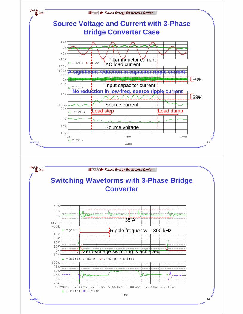
Source Voltage and Current with 3-Phase Bridge Converter Case
Time
0s 5ms 10msV(Vfc)
10V
20V
30V
-I(Vfc)20A
60A
SEL>>
I(Cin)-50A
0A
50A
100A
150AI(Ld3) V(Iac)
-15A
-5A
5A
15A
Source voltage
Source currentLoad step
Input capacitor current
AC load currentFilter inductor current
A significant reduction in capacitor ripple current
33%
80%
No reduction in low-freq. source ripple current
Load dump
JSL 14
Switching Waveforms with 3-Phase Bridge Converter
Time
4.998ms 5.000ms 5.002ms 5.004ms 5.006ms 5.008ms 5.010msI(M1:d) I(M4:d)
-25A0A25A50A75A100A
V(M1:d)-V(M1:s) V(M1:g)-V(M1:s)-10V0V10V20V30V40V
I(Cin)-50A
0A
25A
50A
SEL>> 35 A
Ripple frequency = 300 kHz
Zero-voltage switching is achieved

JSL 15
Further Expansion to Six-Phase Bridge (V6) Converter
Sou
rce
Act
ive
Lo
ad
Rectifier+LC filterSix-phase bridge converter
HF ACXformer
20V>83A
JSL 16
Key Feature of V6 DC-DC Converter Soft switching with zero-current turn-on and lagging leg zero-voltage turn-on (ZCZVS)
High efficiency operation over a wide load range with a peak efficiency of 98%
Double output voltage with transformer connected in open -Y connection reduce turns ratio and associated leakage inductance
Interleaved multiple phase operation to eliminate input high-frequency current ripple cost and size reduction on input capacitor Cin
Output DC link inductor Lo current ripple elimination cost and size reduction on inductor
Low-frequency (single-phase inverter load) ripple reduction with active dual-loop control better utilization of source energy and size and cost reduction on input capacitor Cin
91%92%93%94%
95%96%97%98%99%
0 1 2 3 4 5 6Input Power (W)
Eff
icie
ncy
Home-madetransformerCommercial
transformer
C
B
A
A. Vin = 25 V using custom-made commercial transformerB. Vin = 50 V using custom-made commercial transformerC. Vin = 50 V using in-house developed transformer

JSL 17
Waveform Comparison between Full-Bridge and V6 Converters
Full Bridge Converter V6 Converter
iL
iL
vd
vd
Secondary inductor current is ripple-less; and in principle, no dc link inductor is needed
Secondary voltage swing is eliminated with <40% voltage overshoot as compared to 250%
JSL 18
Low-Frequency AC Current Ripple Problems
Inverter AC current ripple propagates back to fuel cell Fuel cell requires a higher current handling capability Cost penalty to
fuel cell stack Ripple current can cause hysteresis losses and subsequently more fuel
consumption Cost penalty to fuel consumption State-of-the-art solutions are adding more capacitors or adding an
external active filters Size and cost penalty The solution without cost penalty is to use existing V6 converter with
active ripple cancellation technique to eliminate the ripple No penalty
Lf
Cf RA
BVdc
+
–
Sap
San Sbn
Sbp
Vo
+
–
60Hz
120Hz
AC filter LC
High-side cap.
DC-DCconverter
120Hz
Fuel Cell

JSL 19
Active Ripple Cancellation Technique
vref+–
Rv2Cv1
Cv2
Rv1
Hv
vsense
Vo
+
−RL
Gvc
+–
Vm
PWMd
Lf
Cf
Vd
iLf+–
Rcf+–
Ri2Ci1
Hi
iref
Ri1
isense
Ci2
Gic Vd = dVin
Adding a current loop to regulate the output current
iac (20A/div) 12.7A rms
iac (20A/div) 12.7A rms
iin (20A/div) 168A avg
iin (20A/div) 162A avg
iL (10A/div)iL (10A/div)
vin (10V/div) 20V avg
vin (10V/div) 20V avg
(a) Without ripple reduction (b) With ripple reduction
JSL 20
2. Energy Management Using Bidirectional DC/DC Converter
Fuel Cell, PV, or
HV Battery
LoadDC/DC
converterInverter
DC Bus
Vdc
Iac
feedbacks
Bidirectional dc/dc
converter
Vac
Vbatt• Low voltage battery or super
capacitor controlling DC bus through a bidirectional dc/dc converter.
• The main application is to help start-up and transient conditions for EV, HEV, fuel cell PCS, etc.
LV battery or super capacitor

JSL 21
Circuit Diagram of a 4-Phase Bidirectional DC-DC Converter with Coupled Inductors
• Multiphase interleaved to reduce input and output capacitor current ripples
• Coupled inductors effectively increase the inductance or reduce the core size
• Hard or soft switching can be configured depending on inductor size and switching frequency
L12
L34
S1u S2u
S2d
S3u
S4dVlow
Chigh
S4u
S1d S3d
1=0°
3=90°
2=180°
4=270°
i1
i2
i3
i4
Clow
Vhigh
JSL 22
Timing Diagram of 4-Phase Bidirectional DC-DC Converter
S1u
D D’
S1d
S3u
S2u
S2d
S3d
S4u
S4d
Ts/4
Ts/2Ts
180°
180°
complementary
complementary
complementary
complementary
90°
1.5 kW, 24-48V50 kW200-400 V

JSL 23
Test Setup of a 1.5-kW Bidirectional DC-DC Converter Using Ultra-capacitor and ABC-150
UltracapacitorPack
BidirectionalDC/DC
Converter
ABC-150Channel 2
Voltage Mode
Remote Operating
System
Data AcquisitionCard (NIDAQ)
Screw Terminal Connector Block
Test Computer (PC)
V1
+
–V2
+
–
I1 I2
• Both channels alternate between sinking and sourcing current • The magnitude of the current is based off of the power
command given to the converter.
36 V 48 V
JSL 24
Boost Mode : 1.5-kW Output Power
Input Voltage
36-V
Output Voltage
48-V
Phase Current 10.42-A
Command1.5-kW
Input Current
41.67-A
Output Voltage
Input Voltage
Input Current

JSL 25
Experimental Results of Bidirectional Charging Mode Transition Operation
Input Current
Input Current
Output Current
Output Current
Command Command
In/Out Voltages
In/Out Voltages
JSL 26
Continuous and Discontinuous Conducting Modes (CCM and DCM)
CCM operation
DTs D’Ts
iL
t
L
VV lowhigh L
VlowIpk
iL
t
L
VV lowhigh
L
Vlow
Ipk+
DCM operation
D1Ts D2Ts D3Ts
Iavg
Iavg
RDT
RDT
L ss 22 )1(2
'2
RDT
RDT
L ss 21
22 )1(
22
CCM occurs with • Larger inductance L• Smaller R (heavy load)• Higher switching frequency
DCM occurs with • Smaller inductance L• Larger R (heavy load)• Lower switching frequency
JSL 27
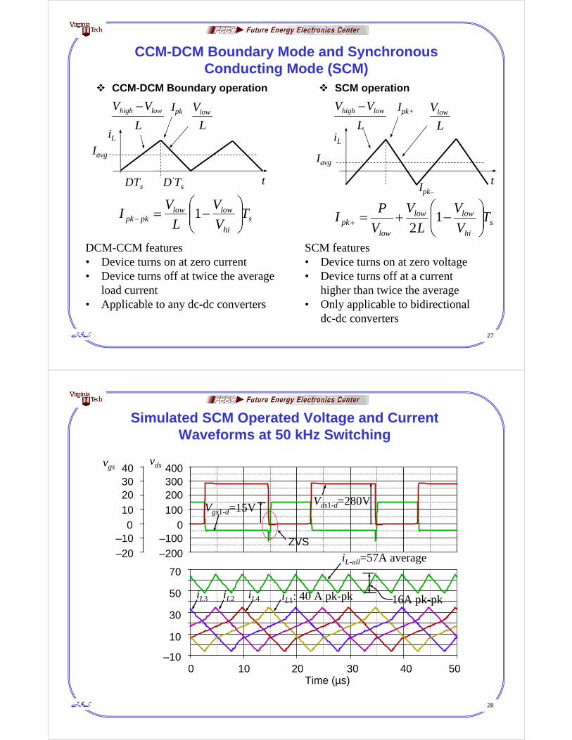
CCM-DCM Boundary Mode and Synchronous Conducting Mode (SCM)
shi
lowlowpkpk T
V
V
L
VI
1
CCM-DCM Boundary operation
shi
lowlow
lowpk T
V
V
L
V
V
PI
1
2
DTs D’Ts
iL
t
L
VV lowhigh L
VlowIpk
iL
t
L
VV lowhigh
L
VlowIpk+
Ipk–
SCM operation
DCM-CCM features • Device turns on at zero current• Device turns off at twice the average
load current• Applicable to any dc-dc converters
SCM features • Device turns on at zero voltage• Device turns off at a current
higher than twice the average• Only applicable to bidirectional
dc-dc converters
Iavg Iavg
JSL 28
Simulated SCM Operated Voltage and Current Waveforms at 50 kHz Switching
Time
9.95ms 9.96ms 9.97ms 9.98ms 9.99ms 10.00msI(RLa)-I(RLb)-I(RLc)-I(RLd) -I(RLa) -I(RLb) -I(RLc) -I(RLd)
-10A
10A20A
30A40A50A60A70A
SEL>>
1 V(M17:g) 2 V(M17:d)20V
10V
0V
10V
20V
30V
40V
-200V
0V
100V
200V
300V
400V2
>>
Vds1-d=280VVgs1-d=15V
iL-all=57A average
iL1: 40 A pk-pk 16A pk-pk
ZVS
0 5010 20 4030
0
100
200
400300
–200
–100
vds
0
10
20
4030
–20
–10
vgs
Time (µs)
10
30
70
50
–10
iL3 iL4iL2

JSL 29
Experimental SCM Operated Voltage and Current Waveforms at 50 kHz Switching
iL: 40 A pk-pk
ZVS
vds-1dvgs-1d
iL-all=57A average 16A pk-pk
iL1 iL3 iL2 iL4
+15V
–5V
280V
DTsD’Ts
Time (5µs/div)
JSL 30
Multiphase Bidirectional DC-DC Converter with Coupled Inductor and SCM Operation
Similar to DCM operation, SCM has a high peak-to-peak inductor current.
With multiphase interleaved, the current ripples cancel each other, and the total current can be significantly reduced.
Device can switch at true zero voltage conduction, thus it is better to use power MOSFET as the switching device.
Turn-off loss can be reduced with a paralleled capacitor (resonant capacitor) across the device.
Coupled inductor allows core loss reduction and increases equivalent inductance.
Overall efficiency can be very high with proper design of inductor and selection of device.

JSL 31
Efficiency of Bidirectional DC-DC Converter Operating in Synchronous Conduction Mode
97.0%
97.5%
98.0%
98.5%
99.0%
99.5%
100.0%
0 5 10 15 20 25 30 35 40 45 50
With 22-kHz frequency
Vlow = 240V, Vhigh = 400V
Power (kW)
Effi
cien
cy (
%) With 20-kHz frequency
• Use two identical 4-phase converters with regenerative connection to measure losses
• One converter operates in buck mode, and the other operates in boost mode
• The total supply power is the loss of two converters, but the output voltage and current are actual load condition.
• Measured peak efficiency exceeds 99.1% at 20 kHz switching.
JSL 32
Possible Efficiency Improvement with Variable Frequency Control
95
96
97
98
99
100
0 5 10 15 20 25 30
20kHz40kHz 30kHz50kHz18kHz
Power (W)
Effi
cien
cy (
%)
• If high efficiency at light load is desired, it is possible to vary the switching frequency.
• High frequency at light load allows much reduced peak current, thus increasing the efficiency.
• Experimental results showed that >99.2% at 50 kHz switching was achieved.

JSL 33
3. High Voltage Conversion Ratio ReboostConverters
Vo=VC1+VC2
• Non-isolated output with high boost ratio
• Suitable for low input voltages such as fuel cells and solar cells
• Significant reduction on switch voltage stress
D
Dn
V
V
in
o
1
1
Flyback
Boost
L
+
Vin
C1
Q1
D11:n
g
+
D2
C2
L+
Vin C
Q1
D11:n
gV1
+
L
C+
V2
Q1
D2
g
s
d
+
Vin
JSL 34
Reboost Converter Operating Modes
Llk1
+
Vin Co
Q1
D11:n
g
+D2
C2
Vo
LM Llk2 Llk1
+
Vin Co
Q1
D11:n
g
+D2
C2
Vo
LM Llk2 Llk1
+
Vin Co
Q1
D11:n
g
+D2
C2
Vo
LM Llk2
(a) Initially, Q1 is off, magnetizing inductor current continues circulating to supply the secondary current. The boost capacitor C2 is discharging to output capacitor Co through diode D1 and Llk2. D2 is off. Vo = VC2+n·VLM. VLk2 = n·VLM = n·Vin. Current in Llk1 reflects the current in Llk2.
(b) Switch Q1 turns on. With reverse biasing, current in D1 starts reducing. Lm is charged. Voltage across Llk2 is VLk2 = n·VLM = Vo–VC2. Since VLM = Vin, VLk2 = nVin.
(c) Current in D1 drops to 0. For non-ideal diodes, there will be a reverse recovery period. Capacitor Co has been charged by sum of voltage across Llk2 and C2. Vo=VC2+nVin. Device Q1 is fully turned on, and Lm current is increasing.
(d) Switch turns off, diode D2 is turned on, and C2 gets charged. After C2 is fully charged, diode D2 will be turned off. Current in Lk2 starts increasing until it reaches steady state.
Llk1
+
Vin Co
Q1
D11:n
g
+D2
C2
Vo
LM Llk2
(a) (d)(c)(b)

JSL 35
Derivation of Voltage Conversion Ratio for the Reboost Converter
• Assume capacitors are large enough that their voltage maintains constant during steady-state operation. Also assume the transformer windings are perfectly coupled.
• During off period (Mode-a and Mode-d), V·s of Lk2 is D’·VLk2. With V·s balance, D’·VLk2= n·D·Vin. Thus VLk2 = n·D·Vin/D’, and VC2 = Vin/D’.
• During on period (Mode-c), Vo = VC2 + nVin. With constant VC2,
ininLkCo VD
nD
D
Dn
DVVVV
'
1
''
122
D
nD
V
V
in
o
1
1The voltage conversion ratio becomes
Actual voltage conversion ratio will be slightly lower with non-perfectly coupled transformer.
JSL 36
0
5
10
15
20
25
30
35
40
0.2 0.3 0.4 0.5 0.6 0.7 0.8
Voltage Conversion Ratio of Reboost DC-DC Converter
Duty cycle
Vol
tage
con
vers
ion
ratio
n=8
n=2
n=4
Boost converter case
Reboostcases

JSL 37
Further Derivation – Recharged Boost Converter
ino VD
DnV
1
1
ino VD
nV
1
2
(a) Reboost converter:• Treat flyback as coupled-
inductor converter
(b) Recharged-boost converter: • Add D3 and C1.• when Q1 turns on, C1 is
charged through D3 and L2.
L
+
Vin
C1
Q1
D11:n
g
+
D2
C2
+
VinCoQ1
D1
g
+D2
C2
L1 L2
+
VinCoQ1
D1
g
+D2
C2
D3
C1L1 L2
JSL 38
Basic Operating Principle of Recharge-Boost Converter
(a) Initially, Q1 is off, magnetizing inductor current charges boost capacitor C2 through diode D2 and output capacitor Co through C1, L2, and D1. D3 is off. Vo = Vin+VLm+VC1+n·VLm. VC2 = Vin+VLm. VL2 = n·VLm. Current in L1 reflects the current in L2.
(b) Switch Q1 turns on. D2 is turned off. Lm is charged. Voltage across L2 is VL2 = n·VLm = Vo–VC1. Since VLm = Vin, VL2 = nVin. With reverse biasing, current in D1 starts reducing.
(c) Current in D1 drops to 0. For non-ideal diodes, there will be a reverse recovery period. Capacitor C1 is charged by sum of voltage across L2 and C2. VC1=VC2+nVin. Device Q1 is fully turned on, and Lm current is increasing.
(d) Switch turns off, diode D2 is turned on, and C2 gets charged with VC2=Vin+VLm. D3 is now reverse-biased, and its current starts reducing. Current in L2 starts reversing until it reaches 0. There will be a reverse recovery period due to non-ideal D3. After that, the mode returns to Mode (a).
+ Co
Q1
D11:n
+
D2 C2
D3
C1 Vo
Vin
Lk1 Lk2
Lm
+
L2L1
+ Co
Q1
D11:n
+
D2 C2
D3
C1 Vo
Vin
Lk1 Lk2
Lm
+
L2L1
+ Co
Q1
D11:n
+
D2 C2
D3
C1 Vo
Vin
Lk1 Lk2
Lm
+
L2L1
+ Co
Q1
D11:n
+
D2 C2
D3
C1 Vo
Vin
Lk1 Lk2
Lm
+
L1 L2
(a) (b) (d)(c)

JSL 39
Derivation of Voltage Conversion Ratio
• Assume capacitors are large enough that their voltage maintains constant during steady-state operation. Also assume the transformer windings are perfectly coupled.
• During off period (Mode-a and Mode-d), V·s of L2 is D’·VL2. With V·s balance, D’·VL2 = n·D·Vin. Thus VL2 = n·D·Vin/D’, and VLm = D·Vin/D’ VC2 = Vin + D·Vin/D’ = (1+D/D’)Vin = Vin/D’.
• During on period (Mode-c), VC1 = VC2 + nVin. With constant VC2, VC1 = (1/D’+n)Vin. • Again with VC1 being constant, under Mode-a condition, we have
''
2
')
'
1(
'
1212 D
n
DV
D
Dnn
DDVVVVV ininLCCo
D
n
V
V
in
o
1
2The voltage conversion ratio becomes
Actual voltage conversion ratio will be slightly lower with non-perfectly coupled transformer.
boost flybackrecharge+
Co
Q1
D11:n
+
D2 C2
D3
C1Vo
Vin
Lk1 Lk2
Lm
+
L1 L2
JSL 40
0
510
15
20
2530
35
4045
50
0.2 0.3 0.4 0.5 0.6 0.7 0.8
Voltage Conversion of Recharged Boost Converter
Duty cycle
Vol
tage
con
vers
ion
ratio
Boost converter case
Reboost case with n=8
Reboost case with n=4
Reboost case with n=2
Recharge boost case with n=8
Recharge boost case with n=4
Recharge boost case with n=2
JSL 41
5.980ms 5.984ms 5.988ms 5.991ms
A
A
A
A
V(M1:g) V(M1:d)
V
V
V
V
V(Vy)-V(Vx) V(Vc) V(Vo)
V
V
V
I(D3) I(D1)
A
A
A
A
V(TX1:1)-V(TX1:2) V(TX1:4)-V(TX1:3)
V
V
V
V
>>
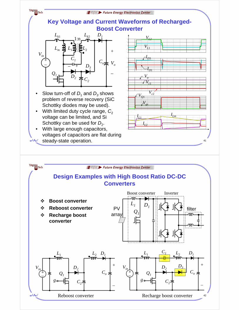
Key Voltage and Current Waveforms of Recharged-Boost Converter
Vo
Vc1
IL2
VQ1
IL1
Vgs
ID3
ID1
• Slow turn-off of D1 and D3 shows problem of reverse recovery (SiCSchottky diodes may be used).
• With limited duty cycle range, C2
voltage can be limited, and Si Schottky can be used for D2.
• With large enough capacitors, voltages of capacitors are flat during steady-state operation.
ILm
Vc2
VL1
VL2
+
Co
Q1
D11:n
+
D2 C2
D3
C1Vo
Vin
Lk1 Lk2
Lm
+
L1 L2
JSL 42
Design Examples with High Boost Ratio DC-DC Converters
Boost converter
Reboost converter
Recharge boost converter
+
VinCoQ1
D1
g
+D2
C2
D3
C1L1 L2
+
VinCoQ1
D1
g
+D2
C2
L1 L2
Reboost converter Recharge boost converter
Q1filterPV
array
D1L1
Boost converter Inverter

JSL 43
Voltage Conversion Ratio and Duty Cycle Constraint
At 10V, Gv = 200/10 = 20, at 20V, Gv = 10
At 60V, Gv = 200/60 = 3.33, 70V, Gv = 200/70 = 2.86
Assume duty cycle is limited to between 0.1 and 0.9
For boost converter case, D at 10 V needs to be 0.95 (difficult to implement)
The reboost converter with n = 8 case has the best suitable duty cycle range for the wide input voltage range case.
For recharge-boost converter with n = 0.58 case, D at 70V needs to be 0.10, not effective utilization of the switch.
PV input 70 V 60 V 20 V 10 V
Boost 0.65 0.70 0.90 0.95
Reboost (n = 8) 0.17 0.22 0.50 0.68
Recharge boost (n = 0.58) 0.10 0.21 0.742 0.87
Duty cycle at different PV voltages
JSL 44
Duty Cycle Comparison Between Boost and Reboost, and Recharge-Boost Converters
0
2
4
6
8
10
12
14
16
18
20
0 0.1 0.2 0.3 0.4 0.5 0.6 0.7 0.8 0.9 1Duty
Vo
ltag
e g
ain
recharge boost with n = 0.58
reboostwith n = 8
boost converter
Duty cycle rangeBoost: 0.65 at 70 V to 0.95 at 10 V Reboost: 0.17 at 70 V to 0.68 at 10 VRecharge boost: 0.10 at 70 V to 0.87 at 10 V
• Boost needs to be excluded due to duty cycle constraint.
• Recharge boost works in theory, but fails in actual implementation at 10 V.

JSL 45
Switch Q1 Voltage Stresses
Both reboost and recharge-boost can be designed to maintain the voltage stress of C2 to below 100 V.
+
VinCoQ1
D1
g
+D2
C2
D3
C1L1 L2
+
VinCoQ1
D1
g
+D2
C2
L1 L2Q1 voltage stress is the voltage across C2 and can be calculated as the boost converter output.
inC VD
V
1
12
a. For boost case, At 10 V input, D = 0.95, VC2 = 200 V, At 70 V input, D = 0.21, VC2 = 200 V,
b. For reboost case with n = 8, At 10 V input, D = 0.68, VC2 = 31 V, At 70 V input, D = 0.17, VC2 = 84 V,
c. For recharge boost case with n = 0.6, At 10 V input, D = 0.87, VC2 = 78 V, At 70 V input, D = 0.10, VC2 = 78 V,
Vo
Vo
JSL 46
Turns Ratio versus Voltage Stress for the ReboostCase
D
nD
V
V
in
o
1
1
36.81
in
clampod
V
VVVn
Therefore, n = 8 should allow reasonable device voltage stress (85 V) and clamping diode voltage stress (700 V).
clampinclampininclampinino nVnVVVD
nVD
DnVV
D
nDV
DV
1
1
1
1
11
1
66.7
inclamp
clamp
inclamp
o
VV
V
VV
Vn
• Assume output diode D1 stress is limited to 700 V
inclampod nVVVV 1
Higher turns ratio, less voltage stress on switch, clamping diode, and clamping capacitor, but higher voltage stress on output diode and more transformer leakage inductance.
Assume Vo = 200 V, Vin_max = 70 V, and Vclamp_max = Vin_max/(1 – D) = 85 V

JSL 47
Simulation results of Voltage stress
With turns ratio n = 8, Vin = 70 V, Vo = 200 V, simulation results agree with the calculated voltage stress of active device and output diode.
Device voltage has small overshoot during turn-off. Additional margin is needed.
(a) Switch voltage (b) Output diode voltage
JSL 48
Simulated Voltages and Device Current at 70-V Input, 100-kHz Switching
0V
200V
SEL>>
V(M1:d)
0V
50V
100V
I(M1:d)
0A
25A
50A
V(M1:d)
>
I(M1:d)
0 1 2 3Time (µs)
4 5 0 1 2 3Time (µs)
4 5
Device voltage
Device current
Output voltage
C2 voltage
(a) Reboost (b) Recharge boost
200 V80 V
85 V 80 V
19 A 44 A
85 V
• Simulation results match the calculated results• Device voltage stress is nearly the same, but the current stress in
recharge boost is much higher due to smaller duty cycle

JSL 49
Diode Current Stresses for Reboost Converter• Assume capacitors and
magnetizing inductance are large enough that capacitor voltages and magnetizing current maintain constant throughout the entire steady-state cycle.
• Average output current Io = Po/Vo = 300/200 = 1.5 A
• At 20-V input, the average input current Iin = 300/20 = 15 A
• With duty cycle D = 0.5, the primary switch current is IQ1 = Iin/D = 22.5 A.
• The output diode current during switch turn-off period is ID1 = Io/D’ = 3 A.
I(D1)
I(M1:d) I(D2) I(Cc)
• Diode D2 conducts when the switch is turned off but only in a very short period to charge the capacitor C2. The peak current of D2 is the peak switch current, or ID2-peak = Isw-peak, but the average ID2 is very small.
5–5
352515
0
–2
4
20
10
2
0
30
0 8642 10Time (µs)
ID1
IQ1
ILM
ILk1
ID2
IC2
JSL 50
Two Phases Interleaved Recharge Boost Converter
+
Vin
CoQ1
Do1
+Dc1
Cc1
L11 L12
Dr1
Cr1
Vo
Q2
Do2
Dc2
Cc2
L21 L22
Dr2
Cr2
Ci
• Multiphase interleaved operation allows ripple reduction • Current sharing among phases is good for high power applications
JSL 51
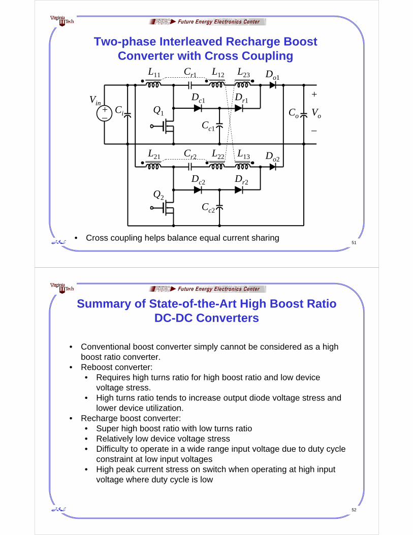
Two-phase Interleaved Recharge Boost Converter with Cross Coupling
+
Vin
CoQ1
Do1
+Dc1
Cc1
L11 L12
Dr1
Cr1
Vo
Q2
Do2
Dc2
Cc2
L21 L22
Dr2
Cr2
Ci
L23
L13
• Cross coupling helps balance equal current sharing
JSL 52
Summary of State-of-the-Art High Boost Ratio DC-DC Converters
• Conventional boost converter simply cannot be considered as a high boost ratio converter.
• Reboost converter: • Requires high turns ratio for high boost ratio and low device
voltage stress. • High turns ratio tends to increase output diode voltage stress and
lower device utilization. • Recharge boost converter:
• Super high boost ratio with low turns ratio • Relatively low device voltage stress • Difficulty to operate in a wide range input voltage due to duty cycle
constraint at low input voltages • High peak current stress on switch when operating at high input
voltage where duty cycle is low
JSL 53
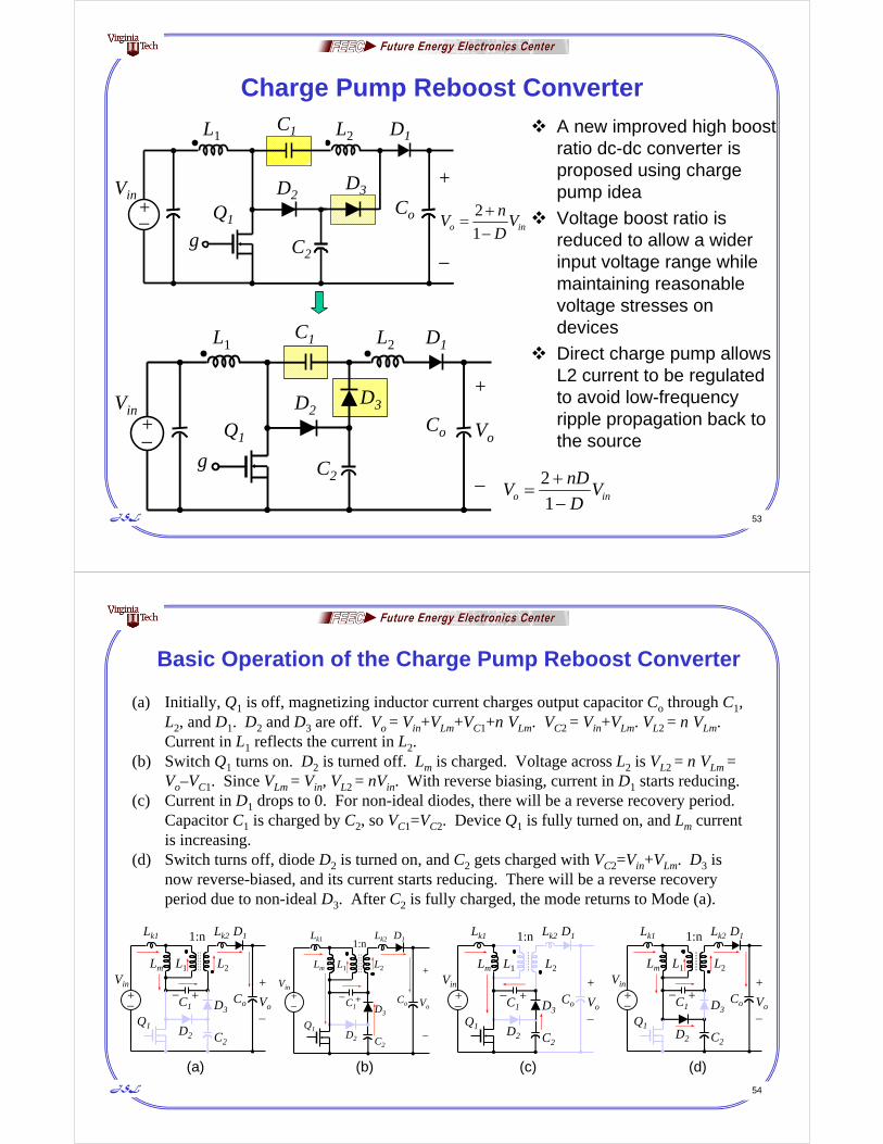
Charge Pump Reboost Converter
A new improved high boost ratio dc-dc converter is proposed using charge pump idea
Voltage boost ratio is reduced to allow a wider input voltage range while maintaining reasonable voltage stresses on devices
Direct charge pump allows L2 current to be regulated to avoid low-frequency ripple propagation back to the source
+
VinCoQ1
D1
g
+D2
C2 ino V
D
nDV
1
2
D3
C1L1 L2
+
VinCoQ1
D1
g
+D2
C2
ino VD
nV
1
2
D3
C1L1 L2
Vo
JSL 54
Basic Operation of the Charge Pump Reboost Converter
(a) Initially, Q1 is off, magnetizing inductor current charges output capacitor Co through C1, L2, and D1. D2 and D3 are off. Vo = Vin+VLm+VC1+n·VLm. VC2 = Vin+VLm. VL2 = n·VLm. Current in L1 reflects the current in L2.
(b) Switch Q1 turns on. D2 is turned off. Lm is charged. Voltage across L2 is VL2 = n·VLm = Vo–VC1. Since VLm = Vin, VL2 = nVin. With reverse biasing, current in D1 starts reducing.
(c) Current in D1 drops to 0. For non-ideal diodes, there will be a reverse recovery period. Capacitor C1 is charged by C2, so VC1=VC2. Device Q1 is fully turned on, and Lm current is increasing.
(d) Switch turns off, diode D2 is turned on, and C2 gets charged with VC2=Vin+VLm. D3 is now reverse-biased, and its current starts reducing. There will be a reverse recovery period due to non-ideal D3. After C2 is fully charged, the mode returns to Mode (a).
(a) (b) (d)(c)
L1
+ Co
Q1
D11:n
C2
D3
C1
+
Vo
D2
Vin
Lk1 Lk2
Lm
+
L2 L1
+ Co
Q1
D11:n
C2
D3
C1
+
Vo
D2
Vin
Lk1 Lk2
Lm
+
L2 L1
+ Co
Q1
D11:n
C2
D3
C1
+
Vo
D2
Vin
Lk1 Lk2
Lm
+
L2
+
Co
Q1
D11:n
+
D2 C2
D3C1 Vo
Vin
Lk1 Lk2
Lm
+
L1 L2

JSL 55
Voltage Conversion Ratio of Charge Pump ReboostConverter
• Assume capacitors are large enough that their voltage maintains constant during steady-state operation. Also assume the transformer windings are perfectly coupled.
• During off period (Mode-a and Mode-d), V·s of L2 is D’·VL2. With V·s balance, D’·VL2 = n·D·Vin. Thus VL2 = n·D·Vin/D’, and VLm = D·Vin/D’ VC2 = Vin + D·Vin/D’ = (1+D/D’)Vin = Vin/D’.
• During on period (Mode-c), VC1 = VC2 = Vin/D’. Under Mode-d condition, we have
''
2
''
1
'
1212 D
nD
DV
D
Dn
DDVVVVV ininLCCo
D
nD
V
V
in
o
1
2The voltage conversion ratio becomes
Actual voltage conversion ratio will be slightly lower with non-perfectly coupled transformer.
boost flybackcharge pump
JSL 56
Voltage Conversion Ratio and Duty Cycle Comparison
0
2
4
6
8
10
12
14
16
18
20
0 0.1 0.2 0.3 0.4 0.5 0.6 0.7 0.8 0.9 1Duty
Vo
ltag
e g
ain
recharge boost with n = 0.58
reboostwith n = 8
Charge-pump re-boost converter n = 2.7
Duty cycle range Reboost: 0.17 at 70V to 0.68 at 10 V Recharge boost: 0.10 at 70 V to 0.88 at 10 V Charge pump reboost: 0.16 at 70 V to 0.8 at 10 V (most suitable range)

JSL 57
0
2
4
6
8
10
12
0 20 40 60 80
Duty Cycle (%)
Vo
lta
ge
Ga
in (V
o /
Vin
)
Measured Gain Predicted Gain
Measured and Calculated Voltage Conversion Ratio
measured
calculated
• Measured voltage conversion ratio matches calculated one very well.
JSL 58
Measured Charge-Pump Reboost Converter Efficiency at Different Voltages
91.0
92.0
93.0
94.0
95.0
96.0
97.0
98.0
0 20 40 60 80 100 120
Eff
icie
nc
y %
% of rated load, 100% = 300W
15V 20V
25V 30V
40V 50V
60V 70V
VT test results with 100V FET, Vo = 200V, 85kHz, n = 2.7
JSL 59
Recap of Part A
A multiphase isolated DC-DC converter with peak efficiency of 98% and significant reduction on high-frequency ripples, thus allowing small-size, low-cost passive components to be used.
Low-frequency ripple is a major issue in maximum energy harness. An active cancellation technique was presented.
Super high efficiency (>99%) can be achieved with bidirectional dc-dc converter operating in synchronous conducting mode.
Different high boost ratio dc-dc converter circuits were presented to show how to design low-cost and high-efficiency converters for renewable energy such as solar panel integration applications.
JSL 60
???
Half-Time Break

JSL 61
Outline – Part B
Part A – High Efficiency DC-DC Converters1. High-Efficiency Low-Ripple Isolated DC-DC Converter
2. Energy Management Using Bidirectional DC/DC Converter3. High Boost Ratio DC-DC Converters
Part B – High Efficiency Inverters1. Half-Cycle Asymmetrical Unipolar PWM
2. Single-Stage Power Conversion
3. Dual Buck Converters
4. H5 Inverter
5. Isolated Single-Stage Design
6. Soft-Switching Inverters
Part C – Energy Efficiency Standards
JSL 62
Outline Part B-1
Part A – High Efficiency DC-DC Converters1. High-Efficiency Low-Ripple Isolated DC-DC Converter
2. Energy Management Using Bidirectional DC/DC Converter3. High Boost Ratio DC-DC Converters
Part B – High Efficiency Inverters1. Half-Cycle Asymmetrical Unipolar PWM
2. Single-Stage Power Conversion
3. Dual Buck Converters
4. H5 Inverter
5. Isolated Single-Stage Design
6. Soft-Switching Inverters
Part C – Energy Efficiency Standards

JSL 63
A Full-Bridge Inverter Circuit
JSL 64
Bipolar Sinusoidal PWM Method Vc: carrier wave vref: reference voltage
S1, S4
S2, S3
vab
vo
timeAlgorithm:
• If vref >vc, turn on upper device; otherwise, turn on lower device.
• If upper device is on then va0= vdc,; otherwise, va0= 0.• van = va0 – vdc/2;

JSL 65
Unipolar (Dual) Sinusoidal PWM Method
time
S1
S2
vab
S4
S3
vc vref-a vref-b
JSL 66
Detailed Waveforms of Unipolar PWM
0
0
Vdc
0
Vdc
0
Vdc
0
–Vdc
va0
vb0
vabSwitching frequency effectively doubled
TsVref-a
Vref-b

JSL 67
PWM Methods in Multi-Stage and Single-Stage Power Conversions
For dc voltage higher than the peak of ac output voltage, a simple dc-ac inverter can be used. However, for dc voltage lower than the peak of ac output voltage, multiple-stage (multiple high-frequency PWM stages) power conversion is needed to obtain the desired ac voltage.
It is possible to convert low-voltage dc to high-voltage ac with a single PWM stage dc-dc converter to obtain high-voltage dc and a polarity selection stage to obtain high-voltage ac.
AC/DCVin
+
–
HFPWM
DC/AC
HFXformer HF
SPWMDC/AC
VacVdc
High-frequency transformer
High-frequency switching
DC/AC inverter
AC/DCVin
+
–
HFPWM
DC/AC
Xformer LFDistri-butionDC/AC
Vac
High-frequency transformer
Low-frequency polarity selection
(b) Single-stage power conversion
(a) Multi-stage power conversion
JSL 68
A Typical Multi-Stage Power Conversion Using Voltage Source Push-Pull DC-DC Converter and Voltage
Source Full-Bridge DC-AC Inverter
dc/ac inverter
PV array ac
output
DC-DC converter
filter
Use voltage source type push-pull dc/dc converter to boost voltage
Entire module can operate independently with one PV array input and one ac output
Multiple ac module outputs can be parallel-connected to utility line

JSL 69
A Typical Multi-Stage Power Conversion Using Current Source Push-Pull DC-DC Converter and Voltage
Source Full-Bridge DC-AC Inverter
dc/ac inverter
PV array
+
–
Vdcac
output
push-pull boost converter
filter
Use current source type push-pull dc/dc converter to boost voltage
Entire module can operate independently with one PV array input and one ac output
Multiple ac module outputs can be parallel-connected to utility line
JSL 70
Single-Stage Inverter with Isolated Converter and a Matrix Converter for Low-Voltage PV Systems
Vin
+
–
HFPWM
DC/AC
Xformer
Vac
High-frequency transformer
• Low-voltage converter implements PWM • Transformer converts high-frequency low-voltage PWM to high voltage • A matrix converter or cycloconverter converts high-frequency ac to
low-frequency ac
ac output
filter
matrix converter

JSL 71
2. Basic Single-Stage Design Idea – A DC-DC Buck Converter + AC Selection Bridge
Features: High input voltage level Buck converter produces rectified SPWM Low frequency selection network produces ac SPWM output Use power MOSFET as the buck switch to reduce switching loss Use IGBT or thyristor as the low-frequency ac selection switch to
avoid reverse recovery loss
Vdc
Vac
LF distribution AC selection network
Buck stage
Filter
JSL 72
Basic Operating Modes of Buck Switch
(a) Positive cycle S1&S4on,S5on
(b) Positive cycle S1&S4on,S5 off, freewheeling
(c) Negative cycle S2&S3 on, M1 on
(d) Negative cycle S2&S3 on, M1off, freewheeling
S5 S5
S5S5
S1
S1
S1
S1
S3
S2
S2S2
S2
S3
S3 S3
S4
S4
S4
S4
• S5 is half-wave symmetrical PWM operated
• Positive cycle, S1and S4 are always on
• Negative cycle, S2 and S3 are always on
S1, S4
S5
S2, S3
vo

JSL 73
3. Dual Buck Type Inverter
Load
i1
i2
io
i2
i1
io
Features:• Use power MOSFET to reduce turn-off loss• Use ultrafast reverse recovery diode to reduce turn-on loss • No dead time and shoot-through concerns • The only issue is power flow is unidirectional, and the output current
must be in phase with the output voltage (reactive power output tends to have distorted current waveform)
Time
60ms 80ms 100ms50msI(RLa) I(RLb)
-20A
0A10A20A
SEL>>
I(RL)-20A-10A
0A10A20A
V(VaL)-200V-100V
0V100V200V vo
vo
JSL 74
Dual Buck Inverter with Dual Outputs
Load1
Load2
Load3
i1
i4
i3
i2
ia

JSL 75
Dual Boost and Dual Buck-Boost Inverters
(a) Double Boost Inverter (b) Double Buck-Boost Inverter
• Use power MOSFET to reduce turn-off loss• Use ultrafast reverse recovery diode to reduce turn-on loss • No dead time and shoot-through concerns
L1
L2
Vdc1
Vdc2
iL
vo
C
R+
–
C
iL
vo
CL1
L2
R+
–
Vdc1
Vdc2 C
JSL 76
Asymmetrical Half-Cycle Unipolar PWM
(a) Positive cycle S1 SPWM, S4 is always on
(b) Negative cycle S3 SPWM, S2 is always on
S1
S1
S1
S1
S3
S2
S2S2
S2
S3
S3 S3
S4
S4
S4
S4
S4
S1
S2
S3
vo
• Split previous buck switch S5 into two PWM operated buck switches, S1 and S3
• Positive cycle, S4 is always on, S1 runs in SPWM
• Negative cycle, S2 is always on, S3 runs in SPWM

JSL 77
4. Asymmetrical Half-Cycle Unipolar PWM Inverter with 5 Switches (H5TM Inverter)
Features:• Buck switch S5 produces rectified SPWM • IGBT’s S1 and S3 serve as low frequency selection network • MOSFET S2 operates in SPWM on negative cycle• MOSFET S4 operates in SPWM on positive cycle• Use fast recovery diode for S1 and S3 to reduce reverse recovery loss• S5 and S2 or S4 share half the DC bus voltage, allowing low-voltage switches
to be used in high voltage input
Vdc
Vac
LF selectionSPWM Buck stage
Filter
S1
S4S2
S3
S3S1
S6
S5
JSL 78
Operating Modes of H5TM Inverter
(a) Positive cycle S1, S4&S5on
(b) Positive cycle S1 on,S4and S5 off, freewheeling
(c) Negative cycle S3, S2&S5on
(d) Negative cycle S2 on, S3 and S5 off, freewheeling
S5 S5
S5S5
S1
S1
S1
S1
S2
S3
S3S3
S3
S2
S2 S2
S4
S4
S4
S4
S1
S4
S2
S3
vo
S5

JSL 79
Measured Gate Signals and Output Voltage Waveforms
S4
S3
S5
AC voltage (100 V/div)
• Experimental results verify the basic operation.
JSL 80
Measured H5 Inverter Efficiency
0.9500.955
0.9600.965
0.9700.9750.980
0.9850.990
0 1 2 3 4 5 6 7 8Power (kW)
Effi
cien
cy
• Use 2 CoolMOS parallel for S5 and S6. They are resistive element, so efficiency is high in low power region.
• Use slow IGBT but ultra fast diode, which can be replaced with SiCSchottky diode to further reduce the MOSFET turn-on loss.
Input: 420 VOutput: 240 V

JSL 81
5. Isolated Single-Stage Design
AC/DCVin
+
–
HFPWM
DC/AC
Xformer LFDistri-butionDC/AC
Vac
High-frequency transformer
Low-frequency switching inverter
• Low-voltage inverter implements symmetrical sinusoidal PWM • Transformer converts high-frequency SPWM to high voltage • Rectifier converts symmetrical SPWM to rectified SPWM • Low-frequency inverter selects the positive and negative cycles, same
as the non-isolated version
JSL 82
Enphase Active-Clamp Flyback Inverter
Q3
D2
D1
Sx2 S2
S1Sx1
Q1
Q2 Q4Q5
• Interleaved flyback converters serve as single-stage power conversion. MOSFET S1 and S2 are the main switches. Sx1and Sx2 are auxiliary switches for active clamp.
• Q1, Q2, Q3, and Q4 thyristors serve as polarity selection switches. Q1 and Q3 turn on during positive cycle. Q2 and Q4turn on during negative cycle.
• Q5 helps commutate thyristors under low dc bus voltage condition.

JSL 83
Measured Efficiency of Enphase Inverter
0.860.870.880.890.900.910.920.930.940.95
0 20 40 60 80 100 120 140 160
Power (W)
Effi
cien
cy
• Use SiC Schottky diode for D1 and D2 to reduce reverse recovery loss• Use low voltage drop thyristors as the polarity selection switch and
block reverse (high) voltage from utility• Use low conduction voltage drop CoolMOS Q5 to help turn off thyristors
at low voltage or zero voltage crossing.
JSL 84
Features of Single-Stage Power Conversion
Reduced power conversion stages with only one PWM stage needed, potentially low cost
High efficiency due to reduced PWM operation
Low frequency ripple propagates back to source without any buffer
A large capacitor bank is needed at the source to ensure maximum power tracking

JSL 85
6. Soft-Switching Inverters
Soft-Switching Basics
Zero-Voltage Switching Type Soft-Switching Inverters
Resonant Snubber Inverter
Coupled-Magnetic Type Zero-Voltage Switching Inverter
JSL 86
Issues with Device Switching
• Problems associated with conventional hard switching– High switching losses Poor
efficiency
– High dv/dt and di/dt Issues with Electromagnetic inference (EMI)
• Major switching losses– Diode reverse recovery induced turn-
on loss
– IGBT turn-off tail current induced turn-off loss
• Soft switching methods– Zero voltage switching (during turn-on)
– Zero current switching (during turn-off)
turn-on turn-off
devicepowerloss
conduction0
devicevoltage 0
devicecurrent 0
Waveforms Showing Device Switching
Behaviors

JSL 87
What’s Relationship Between Snubber and Soft-Switching?
• The traditional snubber uses Ls to limit the turn-on current rise and Cs to limit the turn-off voltage rise. Device losses were reduced, but the snubberlosses were significant. Here are some formula for loss estimation.
Ls
Cs
Llk
sdcsolks
s fVCILL
P2
3)2( 22 Snubber loss
Io
Turn-on loss slks
rdcon f
LL
tVP
)2(24
22
Ls
Cs
Vdc
Turn-off loss ss
fooff f
C
tIP
24
22
• Soft-switching is to do the same job that limits the current rise and voltage rise, but at the same time, to avoid the loss incurred in the snubbers.
JSL 88
Categories of Zero-Voltage Soft-Switching Inverters
Resonant DC Link Resonant PoleAuxiliary Switched Resonant Snubber
Ordinary Resonant Dc Link
Active-Clamp Resonant dc Link
Quasi-Resonant Dc Link
DC Rail Zero-Voltage Transition
Ordinary Resonant Pole
Clamp Mode Resonant Pole (CMRP)
Auxiliary Resonant Commutated Pole (ARCP)
Magnetic Coupled Zero-Voltage Transition
Y-Configured Resonant Snubber Inverter (Y-RSI)
-Configured Resonant Snubber Inverter ( -RSI)
Not easy to achieve 99% efficiency cost effectively

JSL 89
Auxiliary Resonant Commutated Pole (ARCP) Inverter
Lra
LrbVs
C1C3
C4 C6
Lrc
C5
C2
S1 S3 S5
S4 S6 S2Sc
Sb
SaCsp
Csn
R. DeDoncker, 1991
acmotor
Features: Standard PWM applicable Auxiliary switch sees half dc bus
voltage Small size resonant components
Disadvantages: Extra bulk energy storage capacitors Unbalanced capacitor voltages Need complicated control for zero-
voltage switching
JSL 90
Single-Phase Resonant Snubber Soft-Switching Inverter with One Inductor
Lr
Vdc
LoRo
C1
C2C4
S1
S2 S4Sr2
Sr1
ILr2
ILr1
IoIS1
IS3
D1
D2 D4
C3S3
D3
IS2
IS4Dr1
Dr2
a b

JSL 91
Operation Modes of the Single-Phase Resonant Snubber Soft Switching Inverter
S2,3 S1,4
IC1,4
Sr2
IC2,3
IS1,4
IS2,3
Io
ILr2
IC1,4
IC2,3
0
0
0
0
0
t0 t2 t3t4 t5 t6t1
Mode 0: t0 ~ t1
Lr1
VdcLoRo
S1
S2 S4Sr2
Io
S3
IS3
Dr1
Dr2Lr2
Sr1
Lr1
VdcLoRo
S1
S2 S4Sr2
ILr2
Io
S3
IS3
Dr1
Dr2Lr2
Sr1
Mode 1: t1 ~ t2
JSL 92
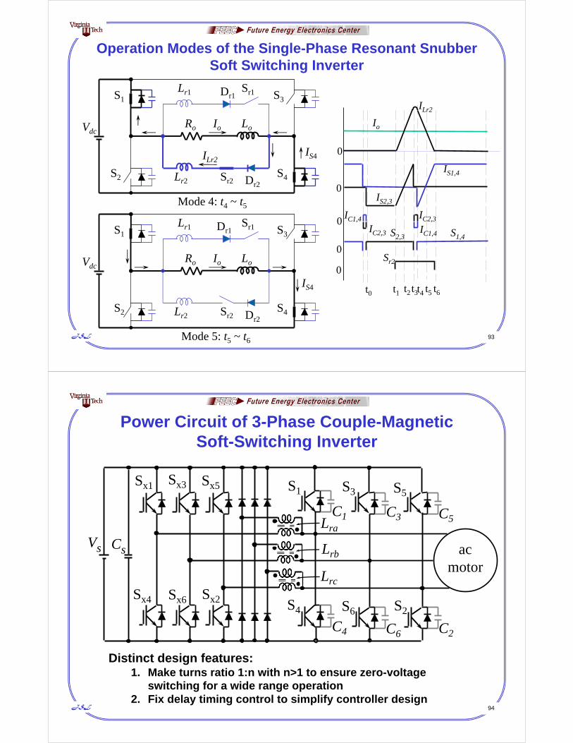
Operation Modes of the Single-Phase Resonant SnubberSoft Switching Inverter
S2,3 S1,4
IC1,4
Sr2
IC2,3
IS1,4
IS2,3
Io
ILr2
IC1,4
IC2,3
0
0
0
0
0
t0 t2 t3t4 t5 t6t1
Mode 2: t2 ~ t3
Lr1
VdcLoRo
S1
S2 S4Sr2
ILr2
Io
S3
IS3
Dr1
Dr2Lr2
Sr1
Lr1
VdcLoRo
S1
S2 S4Sr2
ILr2
Io
S3
IS3
Dr1
Dr2Lr2
Sr1
Mode 3: t3 ~ t4
JSL 93
Operation Modes of the Single-Phase Resonant SnubberSoft Switching Inverter
Mode 5: t5 ~ t6
Mode 4: t4 ~ t5
S2,3 S1,4
IC1,4
Sr2
IC2,3
IS1,4
IS2,3
Io
ILr2
IC1,4
IC2,3
0
0
0
0
0
t0 t2 t3t4 t5 t6t1
Lr1
VdcLoRo
S1
S2 S4Sr2
ILr2
Io
S3
IS4
Dr1
Dr2Lr2
Sr1
Lr1
VdcLoRo
S1
S2 S4Sr2
Io
S3
IS4
Dr1
Dr2Lr2
Sr1
JSL 94
Power Circuit of 3-Phase Couple-Magnetic Soft-Switching Inverter
CsVs acmotor
Sx3 Sx5
Sx4 Sx6 Sx2
Sx1
C1
C4
C3
S1
S4 S6 S2
S5S3
C6
C5
C2
Lra
Lrc
Lrb
Distinct design features: 1. Make turns ratio 1:n with n>1 to ensure zero-voltage
switching for a wide range operation2. Fix delay timing control to simplify controller design
JSL 95
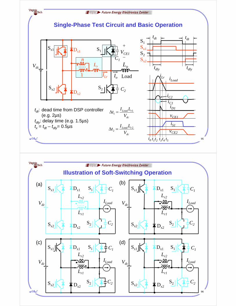
Single-Phase Test Circuit and Basic Operation
Vdc
Sx2
Sx1
C1
C2
S1
S2
Lr
Load
VCE1
ILr Io
tdt: dead time from DSP controller (e.g. 2µs)
tdly: delay time (e.g. 1.5µs)tx = tdt – tdly= 0.5µs
Dx1
Dx2
1
n
S1
Sx1
S2
Sx2
tdt
tdlytdly
tdt
t0 t1t2 t3t4
iC1
iC2
iLr
vCE1
iD1
iS1
iLoad
vCE2dc
rLoad
V
LIt 2
2
dc
rLoad
V
LIt 11
t5
Lo
JSL 96
Illustration of Soft-Switching Operation
Vdc
Sx2
Sx1 C1
C2
S1
S2
ILoad
Dx1
Dx2
Lr1
Lr2
Vdc
Sx2
Sx1 C1
C2
S1
S2
ILoad
Dx1
Dx2
Lr1
Lr2
Vdc
Sx2
Sx1 C1
C2
S1
S2
ILoad
Dx1
Dx2
Lr1
Lr2
Vdc
Sx2
Sx1 C1
C2
S1
S2
ILoad
Dx1
Dx2
Lr1
Lr2
(a)
(c)
(b)
(d)

JSL 97
Soft-Switching Operation (cont’d)
Vdc
Sx2
Sx1 C1
C2
S1
S2
ILoad
Dx1
Dx2
Lr1
Lr2
Vdc
Sx2
Sx1 C1
C2
S1
S2
ILoad
Dx1
Dx2
Lr1
Lr2
(e) (f)
JSL 98
Inverter Photo Showing DC Bus Capacitor and Coupled Magnetic Connections
DSP interface
DC bus barResonant inductor Saturable inductor

JSL 99
Experimental Verification in One Resonant Cycle
-25A
0A
25A
50A
75A
100A
125A
150A
175A
200A
iLr
ILoadiLr1
iLr2
t(.5µs/div)
iLr (100A/div)
ILoad (100A/div)
vCE (200V/div)
vGE (20V/div)
t (0.5µs/div)
JSL 100
Experimental Results of Inverter Operation at 300-V Bus 69-A Load Current
iLr (100A/div)
ILoad (100A/div)
vCE (200V/div)
vGE (20V/div)
t(500µs/div)

JSL 101
Efficiency Test Results with 100-kW Compressor
90%
91%
92%
93%
94%
95%
96%
97%
98%
99%
100%
20 30 40 50 60 70 80 90
Inverter Input Power (kW)
Effi
cien
cy
JSL 102
Efficiency Test Results with a 5-kW Adaptive Timing Zero-Voltage Switching Inverter
91%92%93%94%95%96%97%98%99%
0 1 2 3 4 5 6Output Power (kW)
Effi
cien
cy (
%)
Hard switching
Fixed timing soft switching
Adaptive timing soft switching
• Fixed timing shows poor light load efficiency, worse than hard-switching case • At 20% load (1-kW), the efficiency improvement with variable timing is >3%. • High power output (>4.5 kW), the efficiency difference becomes less visible
but both soft switching shows better efficiency than hard switching case
Resonant inductors
Resonant capacitors
DC bus capacitors
DSP board
AC output
DC input

JSL 103
Features of the Auxiliary Commutated Resonant Snubber Inverters
Main switches turn on at zero voltage or under their anti-parallel diodes conducting condition;
Main switches turn off at a slower dv/dt rate and lossless snubbing condition;
Main switches do not have over-voltage or over-current stress; Auxiliary switches conduct only in a short period as compared to the PWM
cycle; Auxiliary switches turn on and off under zero current condition; Auxiliary switches need to carry high peak current, typically higher than the
rated load current; Free wheeling diodes across the main switches do not have reverse
recovery problems because their currents are diverted by the auxiliary resonant circuitry;
Auxiliary circuit diodes need to have very fast reverse recovery characteristic to prevent the resonant current from oscillation when it is swinging down across the zero point.
JSL 104
Recap for Part B
For energy applications, single-stage inverters have been actively studied and extended to different variations of high-efficiency inverter.
High efficiency commercial inverters (SMA and Enphase) are introduced.
Dual buck, dual boost, and dual buck-boost inverters show potential for high efficiency operation.
Soft-switching shows efficiency >99% for 3-phase high-power motor drives and >98% for 1-phase 5-kW grid-tie inverter.

JSL 105
Outline – Part C
Part A – High Efficiency DC-DC Converters1. High-Efficiency Low-Ripple Isolated DC-DC Converter
2. Energy Management Using Bidirectional DC/DC Converter3. High Boost Ratio DC-DC Converters
Part B – High Efficiency Inverters1. Half-Cycle Asymmetrical Unipolar PWM
2. Single-Stage Power Conversion
3. Dual Buck Converters
4. H5 Inverter
5. Isolated Single-Stage Design
6. Soft-Switching Inverters
Part C – Energy Efficiency Standards
JSL 106
Part C. Energy Efficiency Standards
California Energy Commission (CEC)
IEC 61683:1999, First Edition, 1999-11, Photovoltaic systems – Power conditioners – Procedures for measuring efficiency.

JSL 107
Efficiency of Alternative Energy Inverters – California Energy Commission (CEC)
All inverters must meet the requirements in EMERGING RENEWABLES EMERGING RENEWABLES PROGRAM, Final Guidebook, Eighth Edition, Section C Inverters.
There are no set minimum requirements, but the conversion efficiency must be tested and reported to CEC - as defined here.
JSL 108
IEC 61683:1999, Photovoltaic Systems – Power Conditioners Procedure for Measuring Efficiency
This standard describes guidelines for measuring the efficiency of power conditioners used in standalone and utility-interactive photovoltaic systems, where the output of the power conditioner is a stable systems, where the output of the power conditioner is a stable ac voltage of constant frequency or a stable dc voltage.
The efficiency is calculated from a direct measurement of input and output power in the factory.
An isolation transformer is included where it is applicable.
China: GB/T 20514-2006 is based on IEC 61683:1999

JSL 109
CEC and IEC Weighted Efficiency Measurement
0.200.05100%
00.5375%
0.480.2150%
0.100.1230%
0.130.0520%
0.060.0410%
0.0305%
IECCEC
JSL 110
Example Efficiency Measurement Results (A High-Boost Ratio DC-DC Converter Example)

JSL 111
Measured and Weighted Efficiency Plots
JSL 112
Summary of Power Electronics Design for Energy Efficiency at Different Levels
System level – Solar MagicTM, single-stage design
Circuit topology – soft switching converter/inverter, dual buck inverter, multilevel converter
Modulation scheme – phase-shift modulation, synchronous conduction mode
Power device – SiC diode, CoolMOS, hybrid switch
Combination of above – H5 inverters
Control strategy – maximum T/A and maximum efficiency for motor drives

JSL 113
Recap
High-efficiency and high-performance dc-dc converters were discussed in three categories: multiphase isolated dc-dc, bidirectional dc-dc, and high-boost ratio dc-dc converters.
High-efficiency dc-ac inverters were introduced in three categories: Dual buck, dual boost, and dual buck-boost inverters, Single-stage inverter for potential high-efficiency and low-
cost design Soft-switching inverters show promising efficiency for both
motor drive and energy applications.
Efficiency standards in US and Europe are introduced to show how to calculate weighted PCS efficiency.
JSL 114
???


![Deep Learning on Computer Vision Applicationsmedia.ee.ntu.edu.tw/crash_course/2018/dl/dlcv_app.pdf · Image Credit: Wei-Sheng Lai @ UC Merced [1] “Deep Laplacian Pyramid Networks](https://static.fdocuments.in/doc/165x107/602b63b29f4fb3475f365757/deep-learning-on-computer-vision-image-credit-wei-sheng-lai-uc-merced-1-aoedeep.jpg)