Tutorial for the Semi Custom Part of the Image … Design II Tutorial for the Semi Custom Part of...
24
EPFL/STI/IMM/LSM Bâtiment ELD, Station 11 CH-1015 Lausanne Switzerland Fax: +41(21)69-36959 WWW: http://lsm.epfl.ch/ VLSI Design II Tutorial for the Semi Custom Part of the Image Processing System Torsten Mähne * 22 March to 5 April 2007 Laboratoire de Systèmes Microélectroniques (LSM) Contents 1. Introduction 1 1.1. Preparation of the Project Directory .............................. 2 2. Single Port Random Access Memory (RAM) 3 3. Histogram Calculation Block 3 3.1. Session 1: Creation and Simulation of the VHDL model of the histogram block ...... 3 3.2. Session 2: Synthesis of the Gate-Level Netlist of the Histogram Block ........... 5 3.3. Session 3: Placement & Routing of the Histogram Block ................... 6 A. Single Port Random Access Memory (RAM) 6 B. Histogram Block 10 1. Introduction The goal of this tutorial is to get familiar with the Electronic Design Automation (EDA) tools used in a typical semi custom digital design flow. It is based on the tutorial [5] given in the semi-custom part of the practical laboratory for the EDA Based Design Course. It’s principal parts VHDL and Verilog simulation (Chapter 2), Logic synthesis (Chapter 3), and Standard cell placement and routing (Chapter 4) will be repeated for the histogram block as follows: Session 1 (22 March 2007): Creation of the Register Transfer Level (RTL) description in VHDL of the histogram block and its simulation with Mentor Graphics ModelSim Session 2 (29 March 2007): Logic synthesis of a gate-level netlist from the RTL description using Synopsys Design Vision * Phone: +41(21)69-36922, E-Mail: torsten.maehne@epfl.ch vlsi2_semi_custom_tutorial.tex Rev: 3, March 27, 2007 1
Transcript of Tutorial for the Semi Custom Part of the Image … Design II Tutorial for the Semi Custom Part of...

EPFL/STI/IMM/LSMBâtiment ELD, Station 11CH-1015 LausanneSwitzerlandFax: +41(21)69-36959WWW: http://lsm.epfl.ch/
VLSI Design II
Tutorial for the Semi Custom Part of the ImageProcessing System
Torsten Mähne∗
22 March to 5 April 2007Laboratoire de Systèmes Microélectroniques (LSM)
Contents1. Introduction 1
1.1. Preparation of the Project Directory . . . . . . . . . . . . . . . . . . . . . . . . . . . . . . 2
2. Single Port Random Access Memory (RAM) 3
3. Histogram Calculation Block 33.1. Session 1: Creation and Simulation of the VHDL model of the histogram block . . . . . . 33.2. Session 2: Synthesis of the Gate-Level Netlist of the Histogram Block . . . . . . . . . . . 53.3. Session 3: Placement & Routing of the Histogram Block . . . . . . . . . . . . . . . . . . . 6
A. Single Port Random Access Memory (RAM) 6
B. Histogram Block 10
1. IntroductionThe goal of this tutorial is to get familiar with the Electronic Design Automation (EDA) tools used ina typical semi custom digital design flow. It is based on the tutorial [5] given in the semi-custom partof the practical laboratory for the EDA Based Design Course. It’s principal parts VHDL and Verilogsimulation (Chapter 2), Logic synthesis (Chapter 3), and Standard cell placement and routing (Chapter 4)will be repeated for the histogram block as follows:
Session 1 (22 March 2007): Creation of the Register Transfer Level (RTL) description in VHDL of thehistogram block and its simulation with Mentor Graphics ModelSim
Session 2 (29 March 2007): Logic synthesis of a gate-level netlist from the RTL description usingSynopsys Design Vision
∗Phone: +41(21)69-36922, E-Mail: [email protected]
vlsi2_semi_custom_tutorial.tex Rev: 3, March 27, 2007 1
Session 3 (5 April 2007): Automatic placement & routing of the netlist into a layout of the histogramblock using Cadence First Encounter
The semi custom part requires good knowledge about VHDL [1]. The behavioural modelling ofAnalogue-to-Digital Converter (ADC) designed in the analogue part requires knowledge of VHDL-AMS [2].Essential information about the syntax of VHDL [6] and VHDL-AMS [7] and other electronic documentsare available from the Moodle web site (http://moodle.epfl.ch/course/view.php?id=445). The HamburgVHDL Archive [3] provides a collection of free, i.e., public-domain or shareware, VHDL documentation,models, and tools.
1.1. Preparation of the Project DirectoryAll files created by the designer or generated by EDA tools during the course of the Image ProcessingSystem (IPS) project should be organised in directory structure as described in Vachoux [5], Sections 1.2to 1.4. Follow the following steps to create the project directory after logging into immsunsrv2.epfl.chusing one of the edatpx accounts (with x = 1 . . . 10):
1. Create the project hierarchy using the create_eda_project script:
[1]edatp1@immsunsrv2-edatp1> mkdir vlsi2[2]edatp1@immsunsrv2-edatp1> cd vlsi2/[3]edatp1@immsunsrv2-vlsi2> create_eda_project IPS[4]edatp1@immsunsrv2-vlsi2> cd IPS/
2. Set-up the EDA tools to be used in the project by creating or modifying a file called edadk.confin your home directory or the top-level of your project directory (supersedes ~/edadk.conf). Theedadk.conf file should contain the following lines:
edadk.conf1 mgc msim 6.2d2 mgc ams 2006.2a3 snps syn 2005.094 cds soce 4.15 cds ic 5.1.416 cds assura 3.1.67 cds mgc_ams 2006.2a8 dk ams hk370
3. Install the AMS design kit for use with Synopsys Design Vision and Cadence First Encounter byissuing the following command from the top-level of your project directory:
[5]edatp1@immsunsrv2-IPS> ams_setup -p c35b4 -t synopsys_dc[6]edatp1@immsunsrv2-IPS> ams_setup -p c35b4 -t cadence_soce
4. Install the AMS design kit for use with Cadence IC by launching it once with the technologyoption c35b4 from the layout subdirectory LAY/:
[7]edatp1@immsunsrv2-IPS> cd LAY[8]edatp1@immsunsrv2-LAY> ams_cds -t c35b4 -m fb
When you are asked for the exact process option, select C35B4M6. Quit Cadence IC by selectingExit. . . from the File menu of the icfb.
5. Change back to the top-level of the project directory:
[9]edatp1@immsunsrv2-LAY> cd ..
Remember: All EDA tools need to be launched from the top-level of the project directory tofind their configuration files except for Cadence IC, which needs to be launched always from theLAY/ subdirectory.
2 Rev: 3, March 27, 2007 vlsi2_semi_custom_tutorial.tex
Table 1: Interface of the Random Access Memory (RAM)
(a) Generics
Name Type Default DescriptionNBITS_WORD positive 8 Bits of a wordSIZE positive 256 Number of wordsNBITS_ADDRESS positive 8 Bits of address
(b) Ports
Name Class Dir. Type Descriptionclock signal in std_logic Clock inputreset signal in std_logic Asynchronous reset (ac-
tive low)enable signal in std_logic Enable RAM operationrw_select signal in std_logic Select read ’0’ or write ’1’
modeaddress signal in std_logic_vector(NBITS_ADDRESS - 1 downto 0) Address to read from or
write todata_in signal in std_logic_vector(NBITS_WORD - 1 downto 0) Data inputdata_out signal out std_logic_vector(NBITS_WORD - 1 downto 0) Data output
2. Single Port Random Access Memory (RAM)The histogram block needs a RAM to store the number of occurrences of each gray scale value of a frame.The RAM will be created by the full-custom group during the course of the IPS project, but still thesemi-custom group needs a simulation model, which will also serve as a specification.
The interface of the RAM block consisting of generics to configure the block and the ports to communicatewith the block is given in Table 1. The behaviour of the single port RAM is implemented using asynchronous process with asynchronous active-low reset. If the RAM is enabled with enable = ’1’ andrw_select = ’0’, then a data word is read from the specified address at each positive clock edge andoutput at data_out. If the RAM is enabled with enable = ’1’ and rw_select = ’1’, then the data fromdata_in is written to the specified address at each positive clock edge. The VDHL source code of thesingle port RAM is given in Listing 1.
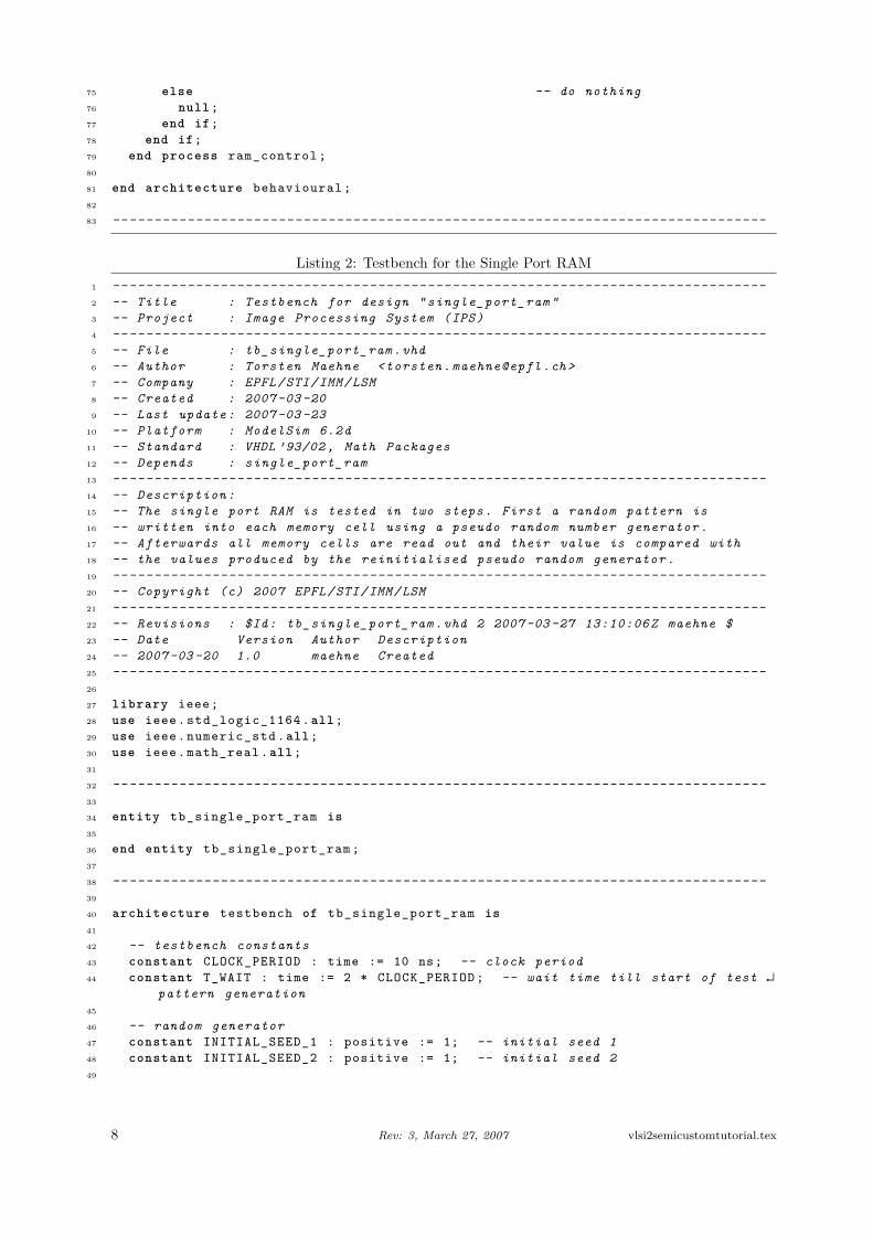
The testbench single port RAM given in Listing 2 carries out the test in two steps. First a randompattern is written into each memory cell using a pseudo random number generator. Afterwards all memorycells are read out and their value is compared with the values produced by the reinitialised pseudo randomnumber generator.
3. Histogram Calculation BlockThe histogram block calculates the histogram from the serial data read from video_in at each positiveedge of the video_clock. Its interface definition is given in Table 2. The calculation is restarted aftera frame_start has been signalled. It then calculates the histogram for the whole frame consisting ofWIDTH * HEIGHT pixels and signals its completion using the done signal. The histogram block relies on anexternal single port RAM (Section 2) to store the histogram.
3.1. Session 1: Creation and Simulation of the VHDL model of the histogramblock
The first task of this tutorial is to create the VHDL model of the histogram calculation block with theinterface from Table 2. The block shall have a asynchronous active-low reset. The histogram calculationis controlled through a synchronous Finite State Machine (FSM) (Figure 1).
vlsi2_semi_custom_tutorial.tex Rev: 3, March 27, 2007 3
Table 2: Interface of the histogram calculation block
(a) Generics
Name Type Default DescriptionWIDTH positive 320 Width of frameHEIGHT positive 240 Height of frameNBITS_PIXEL positive 8 Bits per pixelNBITS_HISTOGRAM positive 18 Bits for each histogram entry
(b) Ports
Name Class Dir. Type Descriptionclock signal in std_logic Clockreset signal in std_logic Reset (active low)frame_start signal in std_logic Frame startvideo_clock signal in std_logic Video clockvideo_in signal in std_logic_vector(NBITS_PIXEL - 1 downto 0) Digitised video sig-
naldone signal out std_logic Histogram doneread_request signal in std_logic Read request for
the histogram dataaddress signal in std_logic_vector(NBITS_PIXEL - 1 downto 0) Address to read
fromdata_out signal out std_logic_vector(NBITS_HISTOGRAM - 1 downto 0) Output for his-
togram dataram_rw_select signal out std_logic Read or write mode
select for RAMram_enable signal out std_logic Enable signal for
RAMram_address signal out std_logic_vector(NBITS_PIXEL - 1 downto 0) Address for RAMram_data_in signal in std_logic_vector(NBITS_HISTOGRAM - 1 downto 0) Data read from
RAMram_data_out signal out std_logic_vector(NBITS_HISTOGRAM - 1 downto 0) Data written to
RAMram_reset signal out std_logic Reset for RAM (ac-
tive low)
4 Rev: 3, March 27, 2007 vlsi2_semi_custom_tutorial.tex
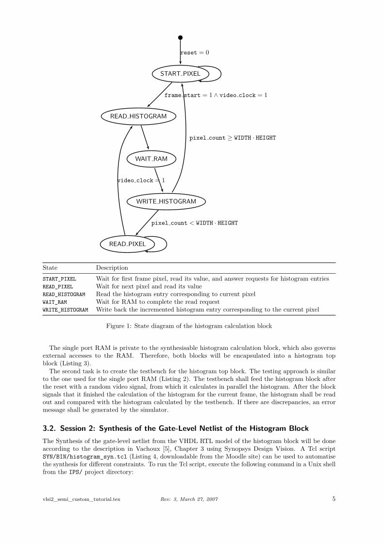
reset = 0
frame start = 1 ∧ video clock = 1
pixel count < WIDTH · HEIGHT
pixel count ≥ WIDTH · HEIGHT
video clock = 1
START PIXEL
READ PIXEL
READ HISTOGRAM
WAIT RAM
WRITE HISTOGRAM
State DescriptionSTART_PIXEL Wait for first frame pixel, read its value, and answer requests for histogram entriesREAD_PIXEL Wait for next pixel and read its valueREAD_HISTOGRAM Read the histogram entry corresponding to current pixelWAIT_RAM Wait for RAM to complete the read requestWRITE_HISTOGRAM Write back the incremented histogram entry corresponding to the current pixel
Figure 1: State diagram of the histogram calculation block
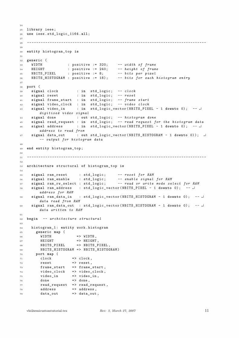
The single port RAM is private to the synthesisable histogram calculation block, which also governsexternal accesses to the RAM. Therefore, both blocks will be encapsulated into a histogram topblock (Listing 3).
The second task is to create the testbench for the histogram top block. The testing approach is similarto the one used for the single port RAM (Listing 2). The testbench shall feed the histogram block afterthe reset with a random video signal, from which it calculates in parallel the histogram. After the blocksignals that it finished the calculation of the histogram for the current frame, the histogram shall be readout and compared with the histogram calculated by the testbench. If there are discrepancies, an errormessage shall be generated by the simulator.
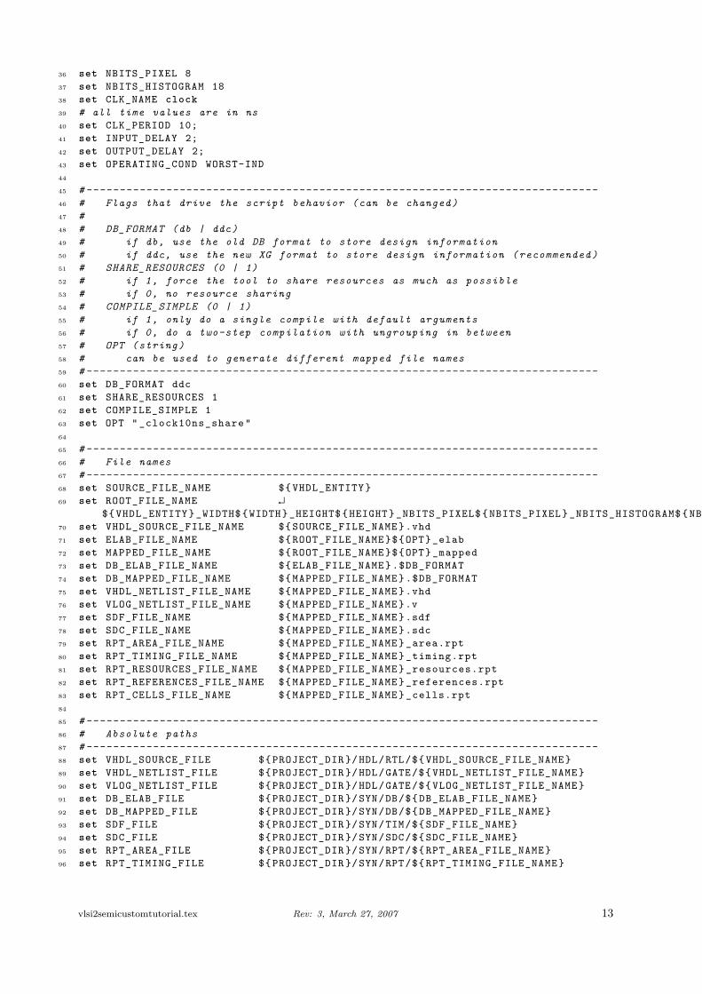
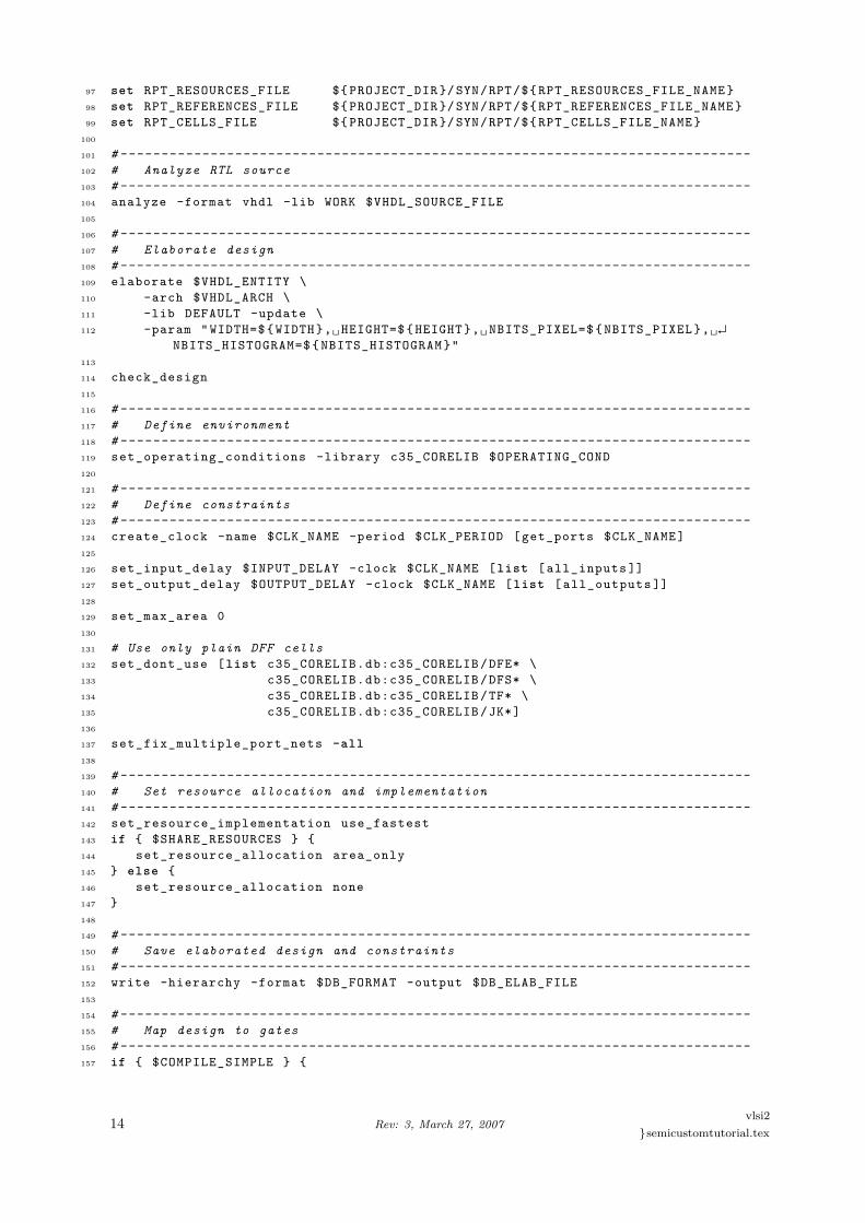
3.2. Session 2: Synthesis of the Gate-Level Netlist of the Histogram BlockThe Synthesis of the gate-level netlist from the VHDL RTL model of the histogram block will be doneaccording to the description in Vachoux [5], Chapter 3 using Synopsys Design Vision. A Tcl scriptSYN/BIN/histogram_syn.tcl (Listing 4, downloadable from the Moodle site) can be used to automatisethe synthesis for different constraints. To run the Tcl script, execute the following command in a Unix shellfrom the IPS/ project directory:
vlsi2_semi_custom_tutorial.tex Rev: 3, March 27, 2007 5

[11]edatp1@immsunsrv2-IPS> dc_shell -f SYN/BIN/histogram_syn.tcl
The Tcl script can serve as a template for synthesis scripts for other digital blocks. An introduction forthe usage of Tcl in the context of (Synopsys) EDA tools is given in Syn [4].
The post-synthesis simulation with Standard Delay Format (SDF) back annotation of the gate delays isdone according to Vachoux [5], Section 2.3 using Mentor Graphics ModelSim. A new histogram_top_syn en-tity with accompagnying testbench tb_histogram_top_syn needs to created as modified versions ofhistogram_top and tb_histogram_top, which now instantiate the synthesised histogram calculation block.The region, to which the SDF file SYN/TIM/histogram_WIDTH320_HEIGHT240_NBITS_PIXEL8_NBITS_HISTOGRAM18_clock10ns_share_mapped.sdf needs to be mapped, is dut:histogram_1 and should beentered in the SDF tab of the Start Simulation dialog of Mentor Graphics ModelSim.
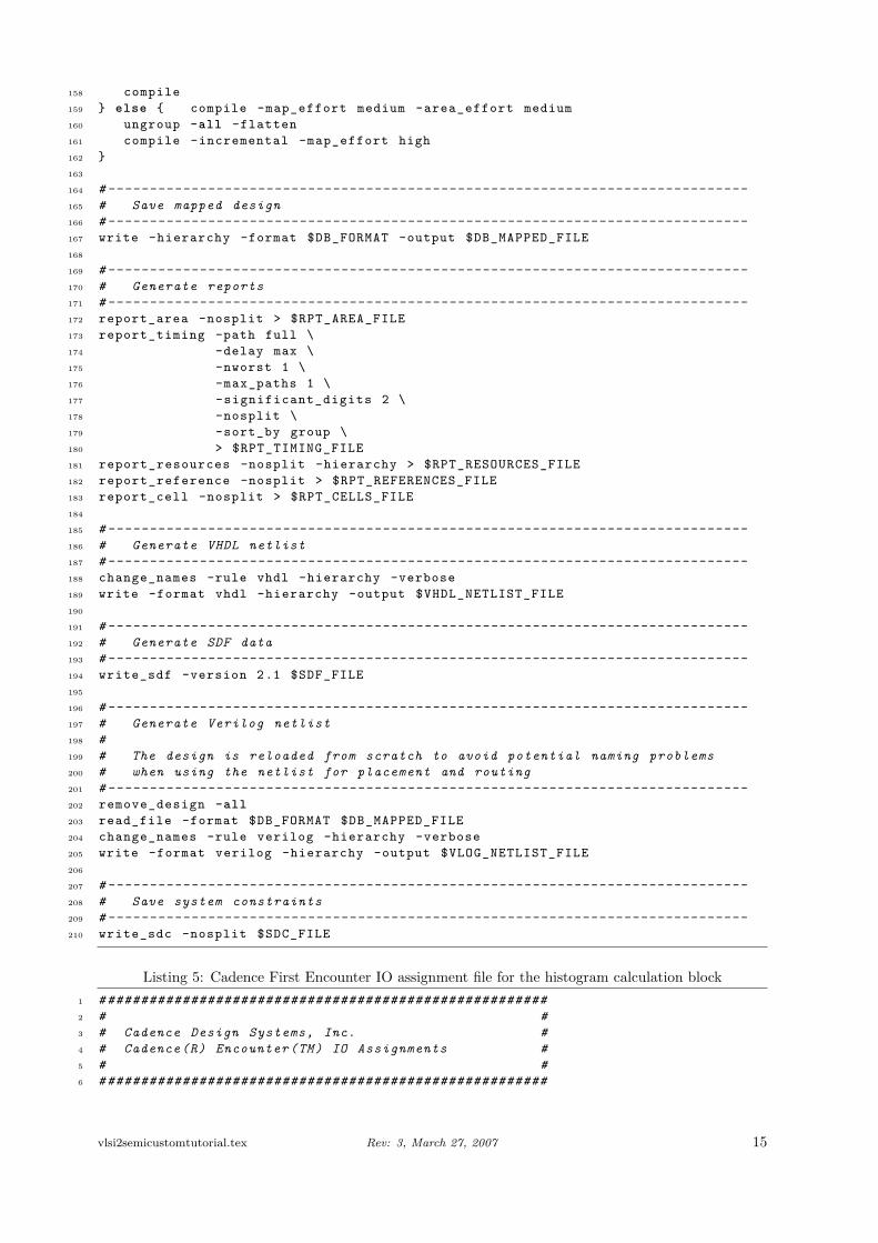
3.3. Session 3: Placement & Routing of the Histogram BlockThe placement and routing of the gate-level netlist of the histogram block will be done accordingto the description in Vachoux [5], Chapter 4 using Cadence First Encounter. A Tcl script PAR/BIN/histogram_par.tcl (Listing 6, downloadable from the Moodle site) can be used to automatise theplacement and routing. Before it can be executed, an Encounter input configuration file PAR/CONF/histogram_WIDTH320_HEIGHT240_NBITS_PIXEL8_NBITS_HISTOGRAM18.conf needs to be created usingthe Design Import. . . Dialog from the File menu of Cadence Encounter as described in Vachoux [5],Section 4.2. An IO file (Listing 5, downloadable from the Moodle site) PAR/CONF/histogram_WIDTH320_HEIGHT240_NBITS_PIXEL8_NBITS_HISTOGRAM18.io controls the placement of the pins and prevents theirplacement on one of the power ring segments, which would lead to Design Rule Checker (DRC) errors. Torun the Tcl script, execute the following command in a Unix shell from the IPS/ project directory:
[13]edatp1@immsunsrv2-IPS> encounter -log PAR/LOG/encounter -overwrite \-init PAR/BIN/histogram_par.tcl -win
The Tcl script can serve as a template for placement and routing scripts for other digital blocks.The post-placement-and-routing simulation with SDF back annotation of the gate delays is done accord-
ing to Vachoux [5], Section 2.4 using the Verilog module of the histogram block generated by Cadence FirstEncounter. A new histogram_top_par entity with accompagnying testbench tb_histogram_top_par needs tocreated as modified versions of histogram_top and tb_histogram_top, which now instantiate the placed androuted histogram calculation block. The region, to which the SDF file PAR/TIM/histogram_WIDTH320_HEIGHT240_NBITS_PIXEL8_NBITS_HISTOGRAM18_clock10ns_cts-routed.sdf needs to be mapped, isdut:histogram_1 and should be entered in the SDF tab of the Start Simulation dialog of MentorGraphics ModelSim.
A. Single Port Random Access Memory (RAM)
Listing 1: VHDL source code of the Single Port RAM1 -- -----------------------------------------------------------------------------2 -- Title : Synchronous Single Port RAM3 -- Project : Image Processing System (IPS)4 -- -----------------------------------------------------------------------------5 -- File : single_port_ram .vhd6 -- Author : Torsten Maehne <torsten . maehne@epfl .ch >7 -- Company : EPFL/STI/IMM/LSM8 -- Created : 2007 -03 -209 -- Last update : 2007 -03 -22
10 -- Platform : ModelSim 6.2d11 -- Standard : VHDL ’93/02 , Math Packages12 -- Depends :13 -- -----------------------------------------------------------------------------14 -- Description :15 -- The behaviour of the single port RAM is implemented using a synchronous16 -- process with asynchronous active -low reset. If the RAM is enabled with17 -- enable = ’1’ and rw_select = ’0’, then a data word is read from the
6 Rev: 3, March 27, 2007 vlsi2semicustomtutorial.tex
18 -- specified address at each positive clock edge and output at data_out . If the19 -- RAM is enabled with enable = ’1’ and rw_select = ’1’, then the data from20 -- data_in is written to the specified address at each positive clock edge.21 -- -----------------------------------------------------------------------------22 -- Copyright (c) 2007 EPFL/STI/IMM/LSM23 -- -----------------------------------------------------------------------------24 -- Revisions : $Id: single_port_ram .vhd 2 2007 -03 -27 13:10:06 Z maehne $25 -- Date Version Author Description26 -- 2007 -03 -20 1.0 maehne Created27 -- -----------------------------------------------------------------------------28
29 library ieee;30 use ieee.std_logic_1164.all;31 use ieee.numeric_std.all;32
33 -- -----------------------------------------------------------------------------34
35 entity single_port_ram is36
37 generic (38 NBITS_WORD : positive := 8; -- bits of a word39 SIZE : positive := 256; -- number of words40 NBITS_ADDRESS : positive := 8); -- bits of address41
42 port (43 signal clock : in std_logic; -- clock input44 signal reset : in std_logic; -- asynchronous reset ( active low)45 signal enable : in std_logic; -- enable RAM operation46 signal rw_select : in std_logic; -- select read ’0’ or write ’1’ mode47 signal address : in std_logic_vector(NBITS_ADDRESS - 1 downto 0); -- ↵
address to read from or write to48 signal data_in : in std_logic_vector(NBITS_WORD - 1 downto 0); -- data ↵
input49 signal data_out : out std_logic_vector(NBITS_WORD - 1 downto 0)); -- ↵
data output50
51 end entity single_port_ram;52
53 -- -----------------------------------------------------------------------------54
55 architecture behavioural of single_port_ram is56
57 begin -- architecture behavioural58
59 -- purpose : control the read and write process to the RAM60 -- type : sequential61 -- inputs : clock , reset , enable , rw_select , address62 -- outputs : data_out63 ram_control : process (clock , reset) is64 type word_vector is array (natural range <>) of ↵
std_logic_vector(NBITS_WORD - 1 downto 0);65 variable memory : word_vector (0 to SIZE - 1) := (others => (others => ↵
’0’)); -- memory66 begin -- process ram_fsm67 if reset = ’0’ then -- asynchronous reset ( active low)68 memory := (others => (others => ’0’));69 data_out <= (others => ’0’);70 elsif clock ’event and clock = ’1’ then -- rising clock edge71 if enable = ’1’ and rw_select = ’0’ then -- read from RAM72 data_out <= memory(to_integer(unsigned(address)));73 elsif enable = ’1’ and rw_select = ’1’ then -- write to RAM74 memory(to_integer(unsigned(address))) := data_in;
vlsi2semicustomtutorial.tex Rev: 3, March 27, 2007 7
75 else -- do nothing76 null;77 end if;78 end if;79 end process ram_control;80
81 end architecture behavioural;82
83 -- -----------------------------------------------------------------------------
Listing 2: Testbench for the Single Port RAM1 -- -----------------------------------------------------------------------------2 -- Title : Testbench for design " single_port_ram "3 -- Project : Image Processing System (IPS)4 -- -----------------------------------------------------------------------------5 -- File : tb_single_port_ram .vhd6 -- Author : Torsten Maehne <torsten . maehne@epfl .ch >7 -- Company : EPFL/STI/IMM/LSM8 -- Created : 2007 -03 -209 -- Last update : 2007 -03 -23
10 -- Platform : ModelSim 6.2d11 -- Standard : VHDL ’93/02 , Math Packages12 -- Depends : single_port_ram13 -- -----------------------------------------------------------------------------14 -- Description :15 -- The single port RAM is tested in two steps. First a random pattern is16 -- written into each memory cell using a pseudo random number generator .17 -- Afterwards all memory cells are read out and their value is compared with18 -- the values produced by the reinitialised pseudo random generator .19 -- -----------------------------------------------------------------------------20 -- Copyright (c) 2007 EPFL/STI/IMM/LSM21 -- -----------------------------------------------------------------------------22 -- Revisions : $Id: tb_single_port_ram .vhd 2 2007 -03 -27 13:10:06 Z maehne $23 -- Date Version Author Description24 -- 2007 -03 -20 1.0 maehne Created25 -- -----------------------------------------------------------------------------26
27 library ieee;28 use ieee.std_logic_1164.all;29 use ieee.numeric_std.all;30 use ieee.math_real.all;31
32 -- -----------------------------------------------------------------------------33
34 entity tb_single_port_ram is35
36 end entity tb_single_port_ram;37
38 -- -----------------------------------------------------------------------------39
40 architecture testbench of tb_single_port_ram is41
42 -- testbench constants43 constant CLOCK_PERIOD : time := 10 ns; -- clock period44 constant T_WAIT : time := 2 * CLOCK_PERIOD; -- wait time till start of test ↵
pattern generation45
46 -- random generator47 constant INITIAL_SEED_1 : positive := 1; -- initial seed 148 constant INITIAL_SEED_2 : positive := 1; -- initial seed 249
8 Rev: 3, March 27, 2007 vlsi2semicustomtutorial.tex
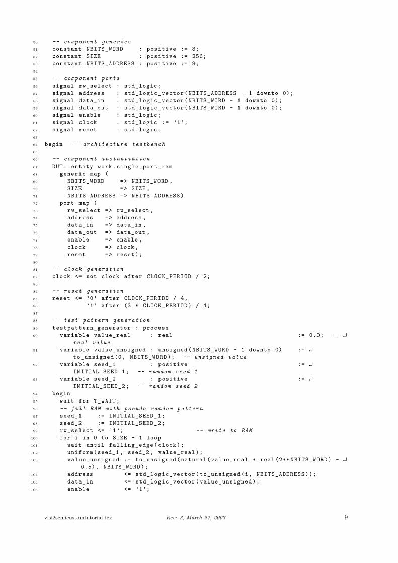
50 -- component generics51 constant NBITS_WORD : positive := 8;52 constant SIZE : positive := 256;53 constant NBITS_ADDRESS : positive := 8;54
55 -- component ports56 signal rw_select : std_logic;57 signal address : std_logic_vector(NBITS_ADDRESS - 1 downto 0);58 signal data_in : std_logic_vector(NBITS_WORD - 1 downto 0);59 signal data_out : std_logic_vector(NBITS_WORD - 1 downto 0);60 signal enable : std_logic;61 signal clock : std_logic := ’1’;62 signal reset : std_logic;63
64 begin -- architecture testbench65
66 -- component instantiation67 DUT: entity work.single_port_ram68 generic map (69 NBITS_WORD => NBITS_WORD ,70 SIZE => SIZE ,71 NBITS_ADDRESS => NBITS_ADDRESS)72 port map (73 rw_select => rw_select ,74 address => address ,75 data_in => data_in ,76 data_out => data_out ,77 enable => enable ,78 clock => clock ,79 reset => reset);80
81 -- clock generation82 clock <= not clock after CLOCK_PERIOD / 2;83
84 -- reset generation85 reset <= ’0’ after CLOCK_PERIOD / 4,86 ’1’ after (3 * CLOCK_PERIOD) / 4;87
88 -- test pattern generation89 testpattern_generator : process90 variable value_real : real := 0.0; -- ↵
real value91 variable value_unsigned : unsigned(NBITS_WORD - 1 downto 0) := ↵
to_unsigned (0, NBITS_WORD); -- unsigned value92 variable seed_1 : positive := ↵
INITIAL_SEED_1; -- random seed 193 variable seed_2 : positive := ↵
INITIAL_SEED_2; -- random seed 294 begin95 wait for T_WAIT;96 -- fill RAM with pseudo random pattern97 seed_1 := INITIAL_SEED_1;98 seed_2 := INITIAL_SEED_2;99 rw_select <= ’1’; -- write to RAM
100 for i in 0 to SIZE - 1 loop101 wait until falling_edge(clock);102 uniform(seed_1 , seed_2 , value_real);103 value_unsigned := to_unsigned(natural(value_real * real (2** NBITS_WORD) - ↵
0.5), NBITS_WORD);104 address <= std_logic_vector(to_unsigned(i, NBITS_ADDRESS));105 data_in <= std_logic_vector(value_unsigned);106 enable <= ’1’;
vlsi2semicustomtutorial.tex Rev: 3, March 27, 2007 9
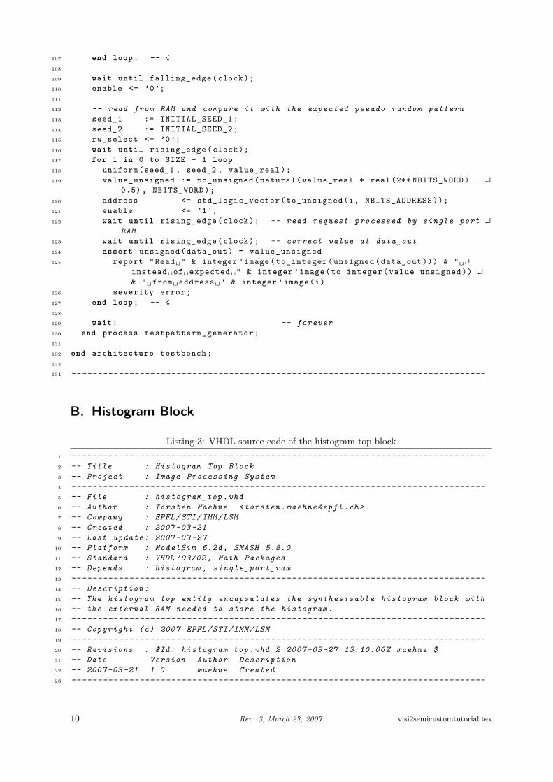
107 end loop; -- i108
109 wait until falling_edge(clock);110 enable <= ’0’;111
112 -- read from RAM and compare it with the expected pseudo random pattern113 seed_1 := INITIAL_SEED_1;114 seed_2 := INITIAL_SEED_2;115 rw_select <= ’0’;116 wait until rising_edge(clock);117 for i in 0 to SIZE - 1 loop118 uniform(seed_1 , seed_2 , value_real);119 value_unsigned := to_unsigned(natural(value_real * real (2** NBITS_WORD) - ↵
0.5), NBITS_WORD);120 address <= std_logic_vector(to_unsigned(i, NBITS_ADDRESS));121 enable <= ’1’;122 wait until rising_edge(clock); -- read request processed by single port ↵
RAM123 wait until rising_edge(clock); -- correct value at data_out124 assert unsigned(data_out) = value_unsigned125 report "Read␣" & integer ’image(to_integer(unsigned(data_out))) & "␣↵
instead␣of␣expected␣" & integer ’image(to_integer(value_unsigned)) ↵
& "␣from␣address␣" & integer ’image(i)126 severity error;127 end loop; -- i128
129 wait; -- forever130 end process testpattern_generator;131
132 end architecture testbench;133
134 -- -----------------------------------------------------------------------------
B. Histogram Block
Listing 3: VHDL source code of the histogram top block1 -- -----------------------------------------------------------------------------2 -- Title : Histogram Top Block3 -- Project : Image Processing System4 -- -----------------------------------------------------------------------------5 -- File : histogram_top .vhd6 -- Author : Torsten Maehne <torsten . maehne@epfl .ch >7 -- Company : EPFL/STI/IMM/LSM8 -- Created : 2007 -03 -219 -- Last update : 2007 -03 -27
10 -- Platform : ModelSim 6.2d, SMASH 5.8.011 -- Standard : VHDL ’93/02 , Math Packages12 -- Depends : histogram , single_port_ram13 -- -----------------------------------------------------------------------------14 -- Description :15 -- The histogram top entity encapsulates the synthesisable histogram block with16 -- the external RAM needed to store the histogram .17 -- -----------------------------------------------------------------------------18 -- Copyright (c) 2007 EPFL/STI/IMM/LSM19 -- -----------------------------------------------------------------------------20 -- Revisions : $Id: histogram_top .vhd 2 2007 -03 -27 13:10:06 Z maehne $21 -- Date Version Author Description22 -- 2007 -03 -21 1.0 maehne Created23 -- -----------------------------------------------------------------------------
10 Rev: 3, March 27, 2007 vlsi2semicustomtutorial.tex
24
25 library ieee;26 use ieee.std_logic_1164.all;27
28 -- -----------------------------------------------------------------------------29
30 entity histogram_top is31
32 generic (33 WIDTH : positive := 320; -- width of frame34 HEIGHT : positive := 240; -- height of frame35 NBITS_PIXEL : positive := 8; -- bits per pixel36 NBITS_HISTOGRAM : positive := 18); -- bits for each histogram entry37
38 port (39 signal clock : in std_logic; -- clock40 signal reset : in std_logic; -- reset41 signal frame_start : in std_logic; -- frame start42 signal video_clock : in std_logic; -- video clock43 signal video_in : in std_logic_vector(NBITS_PIXEL - 1 downto 0); -- ↵
digitised video signal44 signal done : out std_logic; -- histogram done45 signal read_request : in std_logic; -- read request for the histogram data46 signal address : in std_logic_vector(NBITS_PIXEL - 1 downto 0); -- ↵
address to read from47 signal data_out : out std_logic_vector(NBITS_HISTOGRAM - 1 downto 0)); ↵
-- output for histogram data48
49 end entity histogram_top;50
51 -- -----------------------------------------------------------------------------52
53 architecture structural of histogram_top is54
55 signal ram_reset : std_logic; -- reset for RAM56 signal ram_enable : std_logic; -- enable signal for RAM57 signal ram_rw_select : std_logic; -- read or write mode select for RAM58 signal ram_address : std_logic_vector(NBITS_PIXEL - 1 downto 0); -- ↵
address for RAM59 signal ram_data_in : std_logic_vector(NBITS_HISTOGRAM - 1 downto 0); -- ↵
data read from RAM60 signal ram_data_out : std_logic_vector(NBITS_HISTOGRAM - 1 downto 0); -- ↵
data written to RAM61
62 begin -- architecture structural63
64 histogram_1: entity work.histogram65 generic map (66 WIDTH => WIDTH ,67 HEIGHT => HEIGHT ,68 NBITS_PIXEL => NBITS_PIXEL ,69 NBITS_HISTOGRAM => NBITS_HISTOGRAM)70 port map (71 clock => clock ,72 reset => reset ,73 frame_start => frame_start ,74 video_clock => video_clock ,75 video_in => video_in ,76 done => done ,77 read_request => read_request ,78 address => address ,79 data_out => data_out ,
vlsi2semicustomtutorial.tex Rev: 3, March 27, 2007 11

80 ram_reset => ram_reset ,81 ram_enable => ram_enable ,82 ram_rw_select => ram_rw_select ,83 ram_address => ram_address ,84 ram_data_in => ram_data_in ,85 ram_data_out => ram_data_out);86
87 single_port_ram_1: entity work.single_port_ram88 generic map (89 NBITS_WORD => NBITS_HISTOGRAM ,90 SIZE => 2** NBITS_PIXEL ,91 NBITS_ADDRESS => NBITS_PIXEL)92 port map (93 clock => clock ,94 enable => ram_enable ,95 reset => ram_reset ,96 rw_select => ram_rw_select ,97 address => ram_address ,98 data_in => ram_data_out ,99 data_out => ram_data_in);
100
101 end architecture structural;102
103 -- -----------------------------------------------------------------------------
Listing 4: Synopsys DC Tcl script for the histogram calculation block1 # -----------------------------------------------------------------------------2 # Title : Synopsys DC Tcl script for the histogram calculation block3 # Project : Image Processing System4 # -----------------------------------------------------------------------------5 # File : histogram_syn.tcl6 # Author : Torsten Maehne <[email protected] >7 # Company : EPFL/STI/IMM/LSM8 # Created : 2007 -03-259 # Last update: 2007 -03-25
10 # Platform : Synopsys Design Vision 2005 .0911 # Process : AMS 0.35u CMOS (C35), Hit-Kit 3.7012 # Depends : histogram.vhd13 # -----------------------------------------------------------------------------14 # Description:15 # It is assumed that a project directory structure has already been16 # created using ’create_eda_project ’ and that this synthesis script is17 # executed from the project root directory $PROJECT_DIR18 # -----------------------------------------------------------------------------19 # Copyright (c) 2007 EPFL/STI/IMM/LSM20 # -----------------------------------------------------------------------------21 # Revisions : $Id: histogram_syn.tcl 2 2007 -03-27 13 :10:06Z maehne $22 # Date Version Author Description23 # 2007 -03-25 1.0 maehne Created on the base of addsub_syn.tcl ( vachoux )24 # -----------------------------------------------------------------------------25
26
27 set PROJECT_DIR [pwd]28
29 # -----------------------------------------------------------------------------30 # Design related information (can be changed )31 # -----------------------------------------------------------------------------32 set VHDL_ENTITY histogram33 set VHDL_ARCH behavioural34 set WIDTH 32035 set HEIGHT 240
12 Rev: 3, March 27, 2007 vlsi2semicustomtutorial.tex
36 set NBITS_PIXEL 837 set NBITS_HISTOGRAM 1838 set CLK_NAME clock39 # all time values are in ns40 set CLK_PERIOD 10;41 set INPUT_DELAY 2;42 set OUTPUT_DELAY 2;43 set OPERATING_COND WORST-IND44
45 # -----------------------------------------------------------------------------46 # Flags that drive the script behavior (can be changed )47 #48 # DB_FORMAT (db | ddc)49 # if db, use the old DB format to store design information50 # if ddc, use the new XG format to store design information ( recommended )51 # SHARE_RESOURCES (0 | 1)52 # if 1, force the tool to share resources as much as possible53 # if 0, no resource sharing54 # COMPILE_SIMPLE (0 | 1)55 # if 1, only do a single compile with default arguments56 # if 0, do a two-step compilation with ungrouping in between57 # OPT ( string )58 # can be used to generate different mapped file names59 # -----------------------------------------------------------------------------60 set DB_FORMAT ddc61 set SHARE_RESOURCES 162 set COMPILE_SIMPLE 163 set OPT "_clock10ns_share"64
65 # -----------------------------------------------------------------------------66 # File names67 # -----------------------------------------------------------------------------68 set SOURCE_FILE_NAME ${VHDL_ENTITY}69 set ROOT_FILE_NAME ↵
${VHDL_ENTITY}_WIDTH${WIDTH}_HEIGHT${HEIGHT}_NBITS_PIXEL${NBITS_PIXEL}_NBITS_HISTOGRAM${NBITS_HISTOGRAM}70 set VHDL_SOURCE_FILE_NAME ${SOURCE_FILE_NAME}.vhd71 set ELAB_FILE_NAME ${ROOT_FILE_NAME}${OPT}_elab72 set MAPPED_FILE_NAME ${ROOT_FILE_NAME}${OPT}_mapped73 set DB_ELAB_FILE_NAME ${ELAB_FILE_NAME}.$DB_FORMAT74 set DB_MAPPED_FILE_NAME ${MAPPED_FILE_NAME}.$DB_FORMAT75 set VHDL_NETLIST_FILE_NAME ${MAPPED_FILE_NAME}.vhd76 set VLOG_NETLIST_FILE_NAME ${MAPPED_FILE_NAME}.v77 set SDF_FILE_NAME ${MAPPED_FILE_NAME}.sdf78 set SDC_FILE_NAME ${MAPPED_FILE_NAME}.sdc79 set RPT_AREA_FILE_NAME ${MAPPED_FILE_NAME}_area.rpt80 set RPT_TIMING_FILE_NAME ${MAPPED_FILE_NAME}_timing.rpt81 set RPT_RESOURCES_FILE_NAME ${MAPPED_FILE_NAME}_resources.rpt82 set RPT_REFERENCES_FILE_NAME ${MAPPED_FILE_NAME}_references.rpt83 set RPT_CELLS_FILE_NAME ${MAPPED_FILE_NAME}_cells.rpt84
85 # -----------------------------------------------------------------------------86 # Absolute paths87 # -----------------------------------------------------------------------------88 set VHDL_SOURCE_FILE ${PROJECT_DIR }/HDL/RTL/${VHDL_SOURCE_FILE_NAME}89 set VHDL_NETLIST_FILE ${PROJECT_DIR }/HDL/GATE/${VHDL_NETLIST_FILE_NAME}90 set VLOG_NETLIST_FILE ${PROJECT_DIR }/HDL/GATE/${VLOG_NETLIST_FILE_NAME}91 set DB_ELAB_FILE ${PROJECT_DIR }/SYN/DB/${DB_ELAB_FILE_NAME}92 set DB_MAPPED_FILE ${PROJECT_DIR }/SYN/DB/${DB_MAPPED_FILE_NAME}93 set SDF_FILE ${PROJECT_DIR }/SYN/TIM/${SDF_FILE_NAME}94 set SDC_FILE ${PROJECT_DIR }/SYN/SDC/${SDC_FILE_NAME}95 set RPT_AREA_FILE ${PROJECT_DIR }/SYN/RPT/${RPT_AREA_FILE_NAME}96 set RPT_TIMING_FILE ${PROJECT_DIR }/SYN/RPT/${RPT_TIMING_FILE_NAME}
vlsi2semicustomtutorial.tex Rev: 3, March 27, 2007 13
97 set RPT_RESOURCES_FILE ${PROJECT_DIR }/SYN/RPT/${RPT_RESOURCES_FILE_NAME}98 set RPT_REFERENCES_FILE ${PROJECT_DIR }/SYN/RPT/${RPT_REFERENCES_FILE_NAME}99 set RPT_CELLS_FILE ${PROJECT_DIR }/SYN/RPT/${RPT_CELLS_FILE_NAME}
100
101 # -----------------------------------------------------------------------------102 # Analyze RTL source103 # -----------------------------------------------------------------------------104 analyze -format vhdl -lib WORK $VHDL_SOURCE_FILE105
106 # -----------------------------------------------------------------------------107 # Elaborate design108 # -----------------------------------------------------------------------------109 elaborate $VHDL_ENTITY \110 -arch $VHDL_ARCH \111 -lib DEFAULT -update \112 -param "WIDTH=${WIDTH},␣HEIGHT=${HEIGHT},␣NBITS_PIXEL=${NBITS_PIXEL},␣↵
NBITS_HISTOGRAM=${NBITS_HISTOGRAM}"113
114 check_design115
116 # -----------------------------------------------------------------------------117 # Define environment118 # -----------------------------------------------------------------------------119 set_operating_conditions -library c35_CORELIB $OPERATING_COND120
121 # -----------------------------------------------------------------------------122 # Define constraints123 # -----------------------------------------------------------------------------124 create_clock -name $CLK_NAME -period $CLK_PERIOD [get_ports $CLK_NAME]125
126 set_input_delay $INPUT_DELAY -clock $CLK_NAME [list [all_inputs ]]127 set_output_delay $OUTPUT_DELAY -clock $CLK_NAME [list [all_outputs ]]128
129 set_max_area 0130
131 # Use only plain DFF cells132 set_dont_use [list c35_CORELIB.db:c35_CORELIB/DFE* \133 c35_CORELIB.db:c35_CORELIB/DFS* \134 c35_CORELIB.db:c35_CORELIB/TF* \135 c35_CORELIB.db:c35_CORELIB/JK*]136
137 set_fix_multiple_port_nets -all138
139 # -----------------------------------------------------------------------------140 # Set resource allocation and implementation141 # -----------------------------------------------------------------------------142 set_resource_implementation use_fastest143 if { $SHARE_RESOURCES } {144 set_resource_allocation area_only145 } else {146 set_resource_allocation none147 }148
149 # -----------------------------------------------------------------------------150 # Save elaborated design and constraints151 # -----------------------------------------------------------------------------152 write -hierarchy -format $DB_FORMAT -output $DB_ELAB_FILE153
154 # -----------------------------------------------------------------------------155 # Map design to gates156 # -----------------------------------------------------------------------------157 if { $COMPILE_SIMPLE } {
14 Rev: 3, March 27, 2007vlsi2
}semicustomtutorial.tex
158 compile159 } else { compile -map_effort medium -area_effort medium160 ungroup -all -flatten161 compile -incremental -map_effort high162 }163
164 # -----------------------------------------------------------------------------165 # Save mapped design166 # -----------------------------------------------------------------------------167 write -hierarchy -format $DB_FORMAT -output $DB_MAPPED_FILE168
169 # -----------------------------------------------------------------------------170 # Generate reports171 # -----------------------------------------------------------------------------172 report_area -nosplit > $RPT_AREA_FILE173 report_timing -path full \174 -delay max \175 -nworst 1 \176 -max_paths 1 \177 -significant_digits 2 \178 -nosplit \179 -sort_by group \180 > $RPT_TIMING_FILE181 report_resources -nosplit -hierarchy > $RPT_RESOURCES_FILE182 report_reference -nosplit > $RPT_REFERENCES_FILE183 report_cell -nosplit > $RPT_CELLS_FILE184
185 # -----------------------------------------------------------------------------186 # Generate VHDL netlist187 # -----------------------------------------------------------------------------188 change_names -rule vhdl -hierarchy -verbose189 write -format vhdl -hierarchy -output $VHDL_NETLIST_FILE190
191 # -----------------------------------------------------------------------------192 # Generate SDF data193 # -----------------------------------------------------------------------------194 write_sdf -version 2.1 $SDF_FILE195
196 # -----------------------------------------------------------------------------197 # Generate Verilog netlist198 #199 # The design is reloaded from scratch to avoid potential naming problems200 # when using the netlist for placement and routing201 # -----------------------------------------------------------------------------202 remove_design -all203 read_file -format $DB_FORMAT $DB_MAPPED_FILE204 change_names -rule verilog -hierarchy -verbose205 write -format verilog -hierarchy -output $VLOG_NETLIST_FILE206
207 # -----------------------------------------------------------------------------208 # Save system constraints209 # -----------------------------------------------------------------------------210 write_sdc -nosplit $SDC_FILE
Listing 5: Cadence First Encounter IO assignment file for the histogram calculation block1 # #####################################################2 # #3 # Cadence Design Systems, Inc. #4 # Cadence (R) Encounter (TM) IO Assignments #5 # #6 # #####################################################
vlsi2semicustomtutorial.tex Rev: 3, March 27, 2007 15
7
8 Version: 29
10 # Syntax:11 # Pin: <pin-name > <orientation >12 # where <orientation > may be either one of:13 # n north (top)14 # e east (right)15 # s south ( bottom )16 # w west (left)17
18 Offset: 16.019 Pin: clock w20 Pin: reset w21 Pin: frame_start w22 Pin: video_clock w23 Pin: video_in [7] w24 Pin: video_in [6] w25 Pin: video_in [5] w26 Pin: video_in [4] w27 Pin: video_in [3] w28 Pin: video_in [2] w29 Pin: video_in [1] w30 Pin: video_in [0] w31 Pin: read_request w32 Pin: address [7] w33 Pin: address [6] w34 Pin: address [5] w35 Pin: address [4] w36 Pin: address [3] w37 Pin: address [2] w38 Pin: address [1] w39 Offset: 211.040 Pin: address [0] w41
42 Offset: 16.043 Pin: done e44 Pin: data_out [17] e45 Pin: data_out [16] e46 Pin: data_out [15] e47 Pin: data_out [14] e48 Pin: data_out [13] e49 Pin: data_out [12] e50 Pin: data_out [11] e51 Pin: data_out [10] e52 Pin: data_out [9] e53 Pin: data_out [8] e54 Pin: data_out [7] e55 Pin: data_out [6] e56 Pin: data_out [5] e57 Pin: data_out [4] e58 Pin: data_out [3] e59 Pin: data_out [2] e60 Pin: data_out [1] e61 Offset: 211.062 Pin: data_out [0] e63
64 Offset: 16.065 Pin: ram_reset n66 Pin: ram_enable n67 Pin: ram_rw_select n68 Pin: ram_data_in [17] n
16 Rev: 3, March 27, 2007 vlsi2semicustomtutorial.tex
69 Pin: ram_data_in [16] n70 Pin: ram_data_in [15] n71 Pin: ram_data_in [14] n72 Pin: ram_data_in [13] n73 Pin: ram_data_in [12] n74 Pin: ram_data_in [11] n75 Pin: ram_data_in [10] n76 Pin: ram_data_in [9] n77 Pin: ram_data_in [8] n78 Pin: ram_data_in [7] n79 Pin: ram_data_in [6] n80 Pin: ram_data_in [5] n81 Pin: ram_data_in [4] n82 Pin: ram_data_in [3] n83 Pin: ram_data_in [2] n84 Pin: ram_data_in [1] n85 Pin: ram_data_in [0] n86 Pin: ram_data_out [17] n87 Pin: ram_data_out [16] n88 Pin: ram_data_out [15] n89 Pin: ram_data_out [14] n90 Pin: ram_data_out [13] n91 Pin: ram_data_out [12] n92 Pin: ram_data_out [11] n93 Pin: ram_data_out [10] n94 Pin: ram_data_out [9] n95 Pin: ram_data_out [8] n96 Pin: ram_data_out [7] n97 Pin: ram_data_out [6] n98 Pin: ram_data_out [5] n99 Pin: ram_data_out [4] n
100 Pin: ram_data_out [3] n101 Pin: ram_data_out [2] n102 Pin: ram_data_out [1] n103 Offset: 218.0104 Pin: ram_data_out [0] n
Listing 6: Cadence First Encounter Tcl script for the histogram calculation block1 # -----------------------------------------------------------------------------2 # Title : Cadence Encounter Tcl script for the histogram calculation block3 # Project : Image Processing System4 # -----------------------------------------------------------------------------5 # File : histogram_par.tcl6 # Author : Torsten Maehne <[email protected] >7 # Company : EPFL/STI/IMM/LSM8 # Created : 2007 -03-259 # Last update: 2007 -03-25
10 # Platform : Cadence Encounter 5.211 # Process : AMS 0.35u CMOS (C35), Hit-Kit 3.7012 # Depends : histogram_WIDTH320_HEIGHT240_NBITS_PIXEL8_NBITS_HISTOGRAM18.v13 # histogram_WIDTH320_HEIGHT240_NBITS_PIXEL8_NBITS_HISTOGRAM18.conf14 # histogram_WIDTH320_HEIGHT240_NBITS_PIXEL8_NBITS_HISTOGRAM18.io15 # -----------------------------------------------------------------------------16 # Description:17 # It is assumed that a project directory structure has already been18 # created using ’create_eda_project ’ and that this place and route script is19 # executed from the project root directory $PROJECT_DIR20 # -----------------------------------------------------------------------------21 # Copyright (c) 2007 EPFL/STI/IMM/LSM22 # -----------------------------------------------------------------------------23 # Revisions : $Id: histogram_par.tcl 2 2007 -03-27 13 :10:06Z maehne $
vlsi2semicustomtutorial.tex Rev: 3, March 27, 2007 17
24 # Date Version Author Description25 # 2007 -03-25 1.0 maehne Created on the base of addsub_par.tcl ( vachoux )26 # -----------------------------------------------------------------------------27
28
29 set PROJECT_DIR [pwd]30
31 # -----------------------------------------------------------------------------32 # Design related information (can be changed )33 # -----------------------------------------------------------------------------34 set DESIGN histogram_WIDTH320_HEIGHT240_NBITS_PIXEL8_NBITS_HISTOGRAM1835
36 set TIM_LIBRARY C35_CORELIB37 set TIM_OC_MAX WORST-IND ;# TYPICAL | WORST | WORST-IND38 set TIM_OC_MIN BEST-IND ;# TYPICAL | BEST | BEST-IND39
40 # Floorplan settings41 #42 set FP_ASPECT_RATIO 1.043 set FP_ROW_DENSITY 0.85 ;# percent44 set FP_CORE2IO 16 ;# micron45
46 # Power ring and settings47 #48 set PR_WIDTH 4 ;# micron49 set PR_SPACING 0.6 ;# micron50 set PR_LAYER_TB MET1 ;# top and bottom layer51 set PR_LAYER_LR MET2 ;# left and right layer52
53 # Power stripe settings54 #55 set ST_NUM_SETS 1 ;# number of sets56 set ST_SPACING 1 ;# micron57 set ST_LAYER_V $PR_LAYER_LR58 set ST_WIDTH 2 ;# micron59 set ST_XOFS_R 100 ;# micron60 set ST_XOFS_L 100 ;# micron61
62 # Placement settings63 #64 set PL_EFFORT -high ;# -low | -medium | -high65
66 # Clock tree synthesis settings67 #68 set CTS_BUFFER BUF269 set CTS_INV INV070
71 # Filler cells72 #73 set FILLER_CELLS \74 "FILLRT25␣FILLRT10␣FILLRT5␣FILLRT2␣FILLRT1␣FILL25␣FILL10␣FILL5␣FILL2␣FILL1"75
76 # -----------------------------------------------------------------------------77 # Flags that drive the script behavior (can be changed )78 #79 # ADD_STRIPES (0 | 1)80 # if 1, add stripes81 # PLACE_TIMING (0 | 1)82 # if 1, do a timing driven placement83 # CLOCK_TREE (0 | 1)84 # if 1, create a clock tree85 # CTS_CREATE_SPEC (0 | 1)
18 Rev: 3, March 27, 2007 vlsi2semicustomtutorial.tex
86 # if 1, create a clock tree specification file with default values87 # ROUTE_TIMING (0 | 1)88 # if 1, do a timing driven routing89 # OPT ( string )90 # can be used to have different generated file names91 # -----------------------------------------------------------------------------92 set ADD_STRIPES 193 set PLACE_TIMING 194 set CLOCK_TREE 195 set CTS_CREATE_SPEC 096 set ROUTE_TIMING 197 set OPT "_clock10ns_cts"98
99 # -----------------------------------------------------------------------------100 # File names101 # -----------------------------------------------------------------------------102 set CONF_FILE_NAME ${DESIGN}.conf103 set IO_FILE_NAME ${DESIGN}.io104 set DESIGN_NAME ${DESIGN}${OPT}105 set SAVE_DESIGN_FP_NAME ${DESIGN_NAME}-fplan.enc106 set SAVE_DESIGN_PR_NAME ${DESIGN_NAME}-pring.enc107 set SAVE_DESIGN_PL_NAME ${DESIGN_NAME}-placed.enc108 set SAVE_DESIGN_PF_NAME ${DESIGN_NAME}-placed_filled.enc109 set SAVE_DESIGN_CT_NAME ${DESIGN_NAME}-cts.enc110 set SAVE_DESIGN_RO_NAME ${DESIGN_NAME}-routed.enc111 set TIM_RCDB_NAME ${DESIGN_NAME}.rcdb112 set SDF_FILE_NAME ${DESIGN_NAME}-routed.sdf113 set SPEF_FILE_NAME ${DESIGN_NAME}-routed.spef114 set RPT_CHECK_TA_NAME ${DESIGN_NAME}-checkta.rpt115 set RPT_REPORT_TA_NAME ${DESIGN_NAME}-ta.rpt116 set RPT_SLACK_NAME ${DESIGN_NAME}-slack.rpt117 set RPT_GATE_COUNT_NAME ${DESIGN_NAME}-gate_count.rpt118 set RPT_NOTCH_NAME ${DESIGN_NAME}-notch.rpt119 set RPT_CONN_NAME ${DESIGN_NAME}-conn.rpt120 set RPT_GEOM_NAME ${DESIGN_NAME}-geom.rpt121 set RPT_DENSITY_NAME ${DESIGN_NAME}-density.rpt122 set VLOG_NETLIST_SIM_NAME ${DESIGN_NAME}-routed.v123 set VLOG_NETLIST_LVS_NAME ${DESIGN_NAME}-routed_lvs.v124 set CTS_SPEC_NAME ${DESIGN_NAME}-spec.cts125 set CTS_RGUIDE_NAME ${DESIGN_NAME}-guide.cts126 set CTS_RPT_NAME ${DESIGN_NAME}-cts.rpt127 set GDS_FILE_NAME ${DESIGN_NAME}.gds128
129 # -----------------------------------------------------------------------------130 # Absolute paths131 # -----------------------------------------------------------------------------132 set CONF_FILE ${PROJECT_DIR }/PAR/CONF/${CONF_FILE_NAME}133 set IO_FILE ${PROJECT_DIR }/PAR/CONF/${IO_FILE_NAME}134 set SAVE_DESIGN_FP_FILE ${PROJECT_DIR }/PAR/DB/${SAVE_DESIGN_FP_NAME}135 set SAVE_DESIGN_PR_FILE ${PROJECT_DIR }/PAR/DB/${SAVE_DESIGN_PR_NAME}136 set SAVE_DESIGN_PL_FILE ${PROJECT_DIR }/PAR/DB/${SAVE_DESIGN_PL_NAME}137 set SAVE_DESIGN_PF_FILE ${PROJECT_DIR }/PAR/DB/${SAVE_DESIGN_PF_NAME}138 set SAVE_DESIGN_CT_FILE ${PROJECT_DIR }/PAR/DB/${SAVE_DESIGN_CT_NAME}139 set SAVE_DESIGN_RO_FILE ${PROJECT_DIR }/PAR/DB/${SAVE_DESIGN_RO_NAME}140 set SDF_FILE ${PROJECT_DIR }/PAR/TIM/${SDF_FILE_NAME}141 set SPEF_FILE ${PROJECT_DIR }/PAR/TIM/${SPEF_FILE_NAME}142 set TIM_RCDB_FILE ${PROJECT_DIR }/PAR/TIM/${TIM_RCDB_NAME}143 set RPT_CHECK_TA_FILE ${PROJECT_DIR }/PAR/RPT/${RPT_CHECK_TA_NAME}144 set RPT_REPORT_TA_FILE ${PROJECT_DIR }/PAR/RPT/${RPT_REPORT_TA_NAME}145 set RPT_SLACK_FILE ${PROJECT_DIR }/PAR/RPT/${RPT_SLACK_NAME}146 set RPT_GATE_COUNT_FILE ${PROJECT_DIR }/PAR/RPT/${RPT_GATE_COUNT_NAME}147 set RPT_NOTCH_FILE ${PROJECT_DIR }/PAR/RPT/${RPT_NOTCH_NAME}
vlsi2semicustomtutorial.tex Rev: 3, March 27, 2007 19
148 set RPT_CONN_FILE ${PROJECT_DIR }/PAR/RPT/${RPT_CONN_NAME}149 set RPT_GEOM_FILE ${PROJECT_DIR }/PAR/RPT/${RPT_GEOM_NAME}150 set RPT_DENSITY_FILE ${PROJECT_DIR }/PAR/RPT/${RPT_DENSITY_NAME}151 set VLOG_NETLIST_SIM_FILE ${PROJECT_DIR }/HDL/GATE/${VLOG_NETLIST_SIM_NAME}152 set VLOG_NETLIST_LVS_FILE ${PROJECT_DIR }/HDL/GATE/${VLOG_NETLIST_LVS_NAME}153 set CTS_SPEC_FILE ${PROJECT_DIR }/PAR/CTS/${CTS_SPEC_NAME}154 set CTS_RGUIDE_FILE ${PROJECT_DIR }/PAR/CTS/${CTS_RGUIDE_NAME}155 set CTS_RPT_FILE ${PROJECT_DIR }/PAR/RPT/${CTS_RPT_NAME}156 set GDS_FILE ${PROJECT_DIR }/PAR/DEX/${GDS_FILE_NAME}157 set GDS_MAP_FILE ${PROJECT_DIR }/PAR/DEX/gds2.map158
159 # -----------------------------------------------------------------------------160 # Procedures161 # -----------------------------------------------------------------------------162
163 # make_clock_tree164 #165 proc make_clock_tree create_spec {166
167 global CTS_BUFFER CTS_INV CTS_SPEC_FILE CTS_RGUIDE_FILE CTS_RPT_FILE168
169 if { $create_spec || ![file exists $CTS_SPEC_FILE] } {170 createClockTreeSpec \171 -bufFootprint $CTS_BUFFER \172 -invFootprint $CTS_INV \173 -output $CTS_SPEC_FILE174 }175 specifyClockTree -clkfile $CTS_SPEC_FILE176 ckSynthesis \177 -rguide $CTS_RGUIDE_FILE \178 -report $CTS_RPT_FILE179 optDesign -postCTS -setup -drv -outDir PAR/RPT180
181 } ;# make_clock_tree182
183 # -----------------------------------------------------------------------------184 # Load configuration file185 # -----------------------------------------------------------------------------186 loadConfig $CONF_FILE 0187 commitConfig188
189 # -----------------------------------------------------------------------------190 # Load IO file191 # -----------------------------------------------------------------------------192 loadIoFile $IO_FILE193
194 # -----------------------------------------------------------------------------195 # Set operating conditions196 # -----------------------------------------------------------------------------197 setOpCond \198 -maxLibrary $TIM_LIBRARY -max $TIM_OC_MAX \199 -minLibrary $TIM_LIBRARY -min $TIM_OC_MIN200
201 # -----------------------------------------------------------------------------202 # Set user grids203 # -----------------------------------------------------------------------------204 setPreference ConstraintUserXGrid 0.1205 setPreference ConstraintUserXOffset 0.1206 setPreference ConstraintUserYGrid 0.1207 setPreference ConstraintUserYOffset 0.1208 setPreference SnapAllCorners 1209 setPreference BlockSnapRule 2
20 Rev: 3, March 27, 2007 vlsi2semicustomtutorial.tex
210
211 # -----------------------------------------------------------------------------212 # Define global Power nets - make global connections213 # -----------------------------------------------------------------------------214 clearGlobalNets215 globalNetConnect vdd! -type pgpin -pin vdd! -inst * -module {} -verbose216 globalNetConnect gnd! -type pgpin -pin gnd! -inst * -module {} -verbose217 # globalNetConnect vdd3o! -type pgpin -pin vdd3o! -inst * -module {} -verbose218 # globalNetConnect vdd3r1 ! -type pgpin -pin vdd3r1 ! -inst * -module {} -verbose219 # globalNetConnect vdd3r2 ! -type pgpin -pin vdd3r2 ! -inst * -module {} -verbose220 # globalNetConnect gnd3o! -type pgpin -pin gnd3o! -inst * -module {} -verbose221 # globalNetConnect gnd3r! -type pgpin -pin gnd3r! -inst * -module {} -verbose222
223 # -----------------------------------------------------------------------------224 # Initialize floorplan225 # -----------------------------------------------------------------------------226 floorPlan -r $FP_ASPECT_RATIO \227 $FP_ROW_DENSITY \228 $FP_CORE2IO $FP_CORE2IO $FP_CORE2IO $FP_CORE2IO229 fit230 saveDesign $SAVE_DESIGN_FP_FILE231
232 # -----------------------------------------------------------------------------233 # Create and route power rings and power stripes234 # -----------------------------------------------------------------------------235 addRing \236 -around core \237 -nets { gnd! vdd! } \238 -width_bottom $PR_WIDTH -width_top $PR_WIDTH \239 -width_left $PR_WIDTH -width_right $PR_WIDTH \240 -spacing_bottom $PR_SPACING -spacing_top $PR_SPACING \241 -spacing_left $PR_SPACING -spacing_right $PR_SPACING \242 -layer_bottom $PR_LAYER_TB -layer_top $PR_LAYER_TB \243 -layer_left $PR_LAYER_LR -layer_right $PR_LAYER_LR \244 -center 1 \245 -tl 1 -tr 1 -bl 1 -br 1 -lt 1 -lb 1 -rt 1 -rb 1 \246 -stacked_via_bottom_layer MET1 -stacked_via_top_layer MET4 \247 -threshold 0.7248 if { $ADD_STRIPES } {249 addStripe \250 -nets { gnd! vdd! } \251 -number_of_sets $ST_NUM_SETS \252 -spacing $ST_SPACING \253 -layer $ST_LAYER_V \254 -width $ST_WIDTH \255 -xleft_offset $ST_XOFS_L256 }257 sroute \258 -jogControl { preferWithChanges differentLayer } \259 -nets { gnd! vdd! }260 saveDesign $SAVE_DESIGN_PR_FILE261
262 # -----------------------------------------------------------------------------263 # Add CAP cells264 # -----------------------------------------------------------------------------265 addEndCap -preCap ENDCAPL -postCap ENDCAPR -prefix ENDCAP266
267 # -----------------------------------------------------------------------------268 # Core cell placement269 # -----------------------------------------------------------------------------270 if { $PLACE_TIMING } {271 amoebaPlace $PL_EFFORT -timingdriven
vlsi2semicustomtutorial.tex Rev: 3, March 27, 2007 21
272 } else {273 amoebaPlace $PL_EFFORT274 }275 setDrawMode place276 saveDesign $SAVE_DESIGN_PL_FILE277
278 # -----------------------------------------------------------------------------279 # Create clock tree ( optional )280 # -----------------------------------------------------------------------------281 if { $CLOCK_TREE } {282 make_clock_tree $CTS_CREATE_SPEC283 saveDesign $SAVE_DESIGN_CT_FILE284 }285
286 # -----------------------------------------------------------------------------287 # Route design ( Nanoroute )288 # -----------------------------------------------------------------------------289 if { $ROUTE_TIMING } {290 setNanoRouteMode -quiet -timingEngine CTE291 setNanoRouteMode -quiet -routeWithTimingDriven true292 setNanoRouteMode -quiet -routeTdrEffort 0293 }294 globalDetailRoute295 optDesign -postRoute -setup -drv -outDir PAR/RPT296 saveDesign $SAVE_DESIGN_RO_FILE297 setDrawMode place298
299 # -----------------------------------------------------------------------------300 # Add filler cells301 # -----------------------------------------------------------------------------302 addFiller -cell $FILLER_CELLS -prefix FILLER303 saveDesign $SAVE_DESIGN_PF_FILE304
305 # -----------------------------------------------------------------------------306 # Verifications307 # -----------------------------------------------------------------------------308 fillNotch -report $RPT_NOTCH_FILE309 verifyConnectivity \310 -type all \311 -error 1000 \312 -warning 50 \313 -report $RPT_CONN_FILE314 verifyGeometry \315 -allowSameCellViols \316 -allowRoutingBlkgPinOverlap \317 -allowRoutingCellBlkgOverlap \318 -report $RPT_GEOM_FILE319 verifyMetalDensity \320 -detailed \321 -report $RPT_DENSITY_FILE322
323 # -----------------------------------------------------------------------------324 # Extract parasitics325 # -----------------------------------------------------------------------------326 setExtractRCMode \327 -detail \328 -rcdb $TIM_RCDB_FILE \329 -relative_c_t 0.01 \330 -total_c_t 5.0 \331 -reduce 5332 extractRC333
22 Rev: 3, March 27, 2007 vlsi2semicustomtutorial.tex
334 # -----------------------------------------------------------------------------335 # Generate RC and timing files336 # -----------------------------------------------------------------------------337 rcOut -spef $SPEF_FILE338 delayCal -sdf $SDF_FILE339
340 # -----------------------------------------------------------------------------341 # Generate reports342 # -----------------------------------------------------------------------------343 reportGateCount -outfile $RPT_GATE_COUNT_FILE344
345 # Timings346 #347 setCteReport348 setAnalysisMode -setup -async -skew -noClockTree -sequentialConstProp349 reportAnalysisMode350 buildTimingGraph351 checkTA -verbose > $RPT_CHECK_TA_FILE352 reportTA \353 -format { hpin arc cell delay arrival required slew fanout load } \354 -late \355 -max_points 10 \356 -net \357 > $RPT_REPORT_TA_FILE358
359 # -----------------------------------------------------------------------------360 # Save netlist361 # -----------------------------------------------------------------------------362 saveNetlist -excludeLeafCell $VLOG_NETLIST_SIM_FILE363 saveNetlist -physical $VLOG_NETLIST_LVS_FILE364
365 # -----------------------------------------------------------------------------366 # Save GDS2367 # -----------------------------------------------------------------------------368 streamOut $GDS_FILE \369 -mapFile $GDS_MAP_FILE \370 -libName ADDSUB \371 -structureName $DESIGN_NAME \372 -stripes $ST_NUM_SETS \373 -units 1000 \374 -mode ALL
References[1] Peter J. Ashenden. The Designer’s Guide to VHDL. The Morgan Kaufmann Series in Systems
on Silicon. Morgan Kaufmann Publishers, San Francisco, California, USA, 2 edition, 2002. ISBN1-55860-674-2.
[2] Peter J. Ashenden, Greqory D. Peterson, and Darrell A. Teegarden. The System Designer’s Guide toVHDL-AMS—Analog, Mixed-Signal, and Mixed-Technology Modeling. The Morgan Kaufmann Seriesin Systems on Silicon. Morgan Kaufmann Publishers, San Francisco, California, USA, 1 edition, 2003.
[3] The Hamburg VHDL Archive. Group Technical Aspects of Multimodal Systems (TAMS), Universityof Hamburg, Faculty of Mathematics, Informatics and Natural Sciences, Department Informatics,Group TAMS, Vogt-Kölln-Straße 30, D-22527 Hamburg, Germany, March 2007. URL http://tams-www.informatik.uni-hamburg.de/vhdl/.
[4] Using Tcl With Synopsys R© Tools. Synopsys, Inc., March 2003. Version U-2003.03.
vlsi2_semi_custom_tutorial.tex Rev: 3, March 27, 2007 23

[5] Alain Vachoux. Top-down digital design flow. Laboratoire de Systèmes Microélectroniques (LSM),Ecole Polytechnique Fédérale de Lausanne (EPFL), EPFL/STI/IMM/LSM, Bâtiment ELD, Station 11,CH-1015 Lausanne, Switzerland, November 2006. Version 3.1.
[6] Alain Vachoux. VHDL Instant. Laboratoire de Systèmes Microélectroniques (LSM), Ecole Polytech-nique Fédérale de Lausanne (EPFL), EPFL/STI/IMM/LSM, Bâtiment ELD, Station 11, CH-1015 Lau-sanne, Switzerland, November 2006. Version 3.0.
[7] Alain Vachoux. VHDL-AMS Instant. Laboratoire de Systèmes Microélectroniques (LSM), EcolePolytechnique Fédérale de Lausanne (EPFL), EPFL/STI/IMM/LSM, Bâtiment ELD, Station 11,CH-1015 Lausanne, Switzerland, March 2006. Version 3.0.
24 Rev: 3, March 27, 2007 vlsi2_semi_custom_tutorial.tex