Tutorial for MEMS microphones - st.com · 4 Revision history ... MEMS microphone portfolio ......
20
February 2017 DocID025704 Rev 2 1/20 www.st.com AN4426 Application note Tutorial for MEMS microphones Introduction This application note serves as a tutorial for MEMS microphones, providing general characteristics of these devices, both acoustic and mechanical, as well as summarizing the portfolio available from ST. MEMS microphones target all audio applications where small size, high sound quality, reliability and affordability are key requirements. ST's MEMS microphones are designed, developed and manufactured within ST, creating an industry- unique, vertically integrated supply chain. Both analog and digital-input, top and bottom-port solutions are available. Our best-in-class AOP and SNR make ST’s MEMS microphones suitable for applications that require a very high dynamic range, improving the audio experience in any environment. Matching very tight sensitivity allows optimizing beamforming and noise cancelling algorithms for multi-microphone arrays. Low power consumption allows extending battery life.
Transcript of Tutorial for MEMS microphones - st.com · 4 Revision history ... MEMS microphone portfolio ......
February 2017 DocID025704 Rev 2 1/20
www.st.com
AN4426 Application note
Tutorial for MEMS microphones
Introduction This application note serves as a tutorial for MEMS microphones, providing general characteristics of these devices, both acoustic and mechanical, as well as summarizing the portfolio available from ST.
MEMS microphones target all audio applications where small size, high sound quality, reliability and affordability are key requirements.
ST's MEMS microphones are designed, developed and manufactured within ST, creating an industry-unique, vertically integrated supply chain. Both analog and digital-input, top and bottom-port solutions are available.
Our best-in-class AOP and SNR make ST’s MEMS microphones suitable for applications that require a very high dynamic range, improving the audio experience in any environment. Matching very tight sensitivity allows optimizing beamforming and noise cancelling algorithms for multi-microphone arrays. Low power consumption allows extending battery life.
Contents AN4426
2/20 DocID025704 Rev 2
Contents 1 Mechanical specifications, construction details ........................... 4
2 Acoustic parameters ..................................................................... 11
2.1 Sensitivity ........................................................................................ 11
2.2 Directionality .................................................................................... 11
2.3 SNR ................................................................................................ 12
2.4 Dynamic range and acoustic overload point ................................... 12
2.5 Equivalent input noise ..................................................................... 13
2.6 Frequency response ....................................................................... 15
2.7 Total harmonic distortion ................................................................. 16
2.8 PSRR and PSR ............................................................................... 16
3 MEMS microphone portfolio ......................................................... 17
4 Revision history ............................................................................ 19
AN4426 List of figures
DocID025704 Rev 2 3/20
List of figures Figure 1: MEMS microphone inside package ............................................................................................. 4 Figure 2: MEMS transducer mechanical specifications .............................................................................. 4 Figure 3: Capacitance change principle ..................................................................................................... 5 Figure 4: 4 x 5 package .............................................................................................................................. 5 Figure 5: 3 x 4 metal cap package - bottom port ........................................................................................ 6 Figure 6: 3 x 4 package - top port ............................................................................................................... 6 Figure 7: 2 x 3 package - bottom port ......................................................................................................... 7 Figure 8: Faraday cage in ST’s MEMS microphones ................................................................................. 7 Figure 9: RF immunity simulation ............................................................................................................... 8 Figure 10: EMC test setup .......................................................................................................................... 8 Figure 11: RF test disturbance signal with sinusoidal pattern .................................................................... 9 Figure 12: RF immunity test results - MP34DT04 ...................................................................................... 9 Figure 13: RF test disturbance signal @ 217 Hz burst pattern ................................................................ 10 Figure 14: RF immunity of analog differential microphones ..................................................................... 10 Figure 15: Omnidirectional microphone .................................................................................................... 11 Figure 16: A-weighted filter response ....................................................................................................... 12 Figure 17: Acoustic and electrical relationship - analog ........................................................................... 13 Figure 18: Acoustic and electrical relationship - digital ............................................................................. 14 Figure 19: MP45DT02-M frequency response ......................................................................................... 15 Figure 20: MEMS microphone portfolio .................................................................................................... 17 Figure 21: MEMS microphone notation .................................................................................................... 17
Mechanical specifications, construction details AN4426
4/20 DocID025704 Rev 2
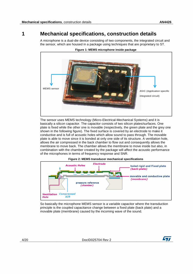
1 Mechanical specifications, construction details A microphone is a dual-die device consisting of two components, the integrated circuit and the sensor, which are housed in a package using techniques that are proprietary to ST.
Figure 1: MEMS microphone inside package
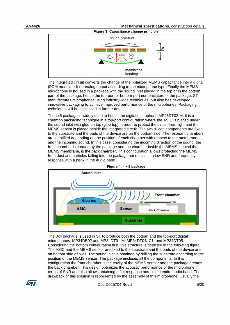
The sensor uses MEMS technology (Micro-Electrical-Mechanical Systems) and it is basically a silicon capacitor. The capacitor consists of two silicon plates/surfaces. One plate is fixed while the other one is movable (respectively, the green plate and the grey one shown in the following figure). The fixed surface is covered by an electrode to make it conductive and is full of acoustic holes which allow sound to pass through. The movable plate is able to move since it is bonded at only one side of its structure. A ventilation hole, allows the air compressed in the back chamber to flow out and consequently allows the membrane to move back. The chamber allows the membrane to move inside but also, in combination with the chamber created by the package will affect the acoustic performance of the microphones in terms of frequency response and SNR.
Figure 2: MEMS transducer mechanical specifications
So basically the microphone MEMS sensor is a variable capacitor where the transduction principle is the coupled capacitance change between a fixed plate (back plate) and a movable plate (membrane) caused by the incoming wave of the sound.
MEMS sensorASIC (Application specific
integrated circuit)
AN4426 Mechanical specifications, construction details
DocID025704 Rev 2 5/20
Figure 3: Capacitance change principle
The integrated circuit converts the change of the polarized MEMS capacitance into a digital (PDM modulated) or analog output according to the microphone type. Finally the MEMS microphone is housed in a package with the sound inlet placed in the top or in the bottom part of the package, hence the top-port or bottom-port nomenclature of the package. ST manufactures microphones using industry-wide techniques, but also has developed innovative packaging to achieve improved performance of the microphones. Packaging techniques will be discussed in further detail.
The 4x5 package is widely used to house the digital microphone MP45DT02-M. It is a common packaging technique in a top-port configuration where the ASIC is placed under the sound inlet with glue on top (glob top) in order to protect the circuit from light and the MEMS sensor is placed beside the integrated circuit. The two silicon components are fixed to the substrate and the pads of the device are on the bottom side. The resonant chambers are identified depending on the position of each chamber with respect to the membrane and the incoming sound. In this case, considering the incoming direction of the sound, the front chamber is created by the package and the chamber inside the MEMS, behind the MEMS membrane, is the back chamber. This configuration allows protecting the MEMS from dust and particles falling into the package but results in a low SNR and frequency response with a peak in the audio band.
Figure 4: 4 x 5 package
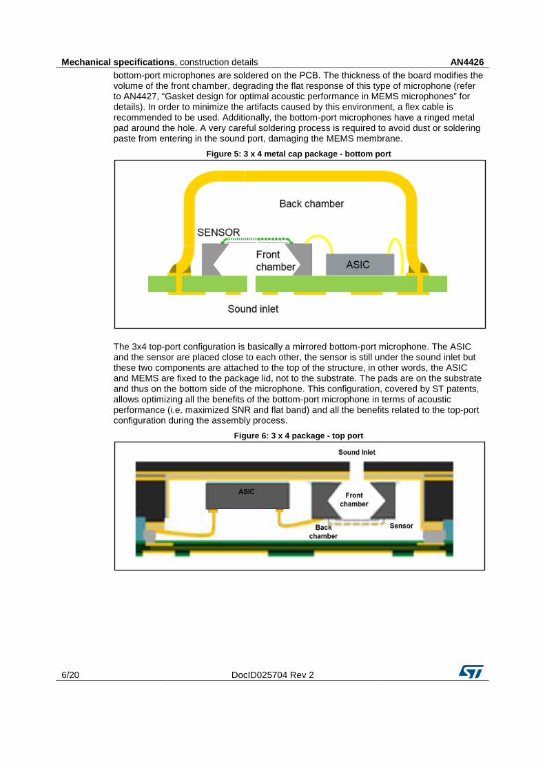
The 3x4 package is used in ST to produce both the bottom and the top-port digital microphones, MP34DB02 and MP34DT01-M, MP34DT04/-C1, and MP34DT05. Considering the bottom configuration first, this structure is depicted in the following figure. The ASIC and the MEMS sensor are fixed to the substrate and the pads of the device are on bottom side as well. The sound inlet is obtained by drilling the substrate according to the position of the MEMS sensor. The package encloses all the components. In this configuration the front chamber is the cavity of the MEMS sensor and the package creates the back chamber. This design optimizes the acoustic performance of the microphone in terms of SNR and also allows obtaining a flat response across the entire audio band. The drawback of this solution is represented by the assembly of this microphone. Usually the
Mechanical specifications, construction details AN4426
6/20 DocID025704 Rev 2
bottom-port microphones are soldered on the PCB. The thickness of the board modifies the volume of the front chamber, degrading the flat response of this type of microphone (refer to AN4427, “Gasket design for optimal acoustic performance in MEMS microphones” for details). In order to minimize the artifacts caused by this environment, a flex cable is recommended to be used. Additionally, the bottom-port microphones have a ringed metal pad around the hole. A very careful soldering process is required to avoid dust or soldering paste from entering in the sound port, damaging the MEMS membrane.
Figure 5: 3 x 4 metal cap package - bottom port
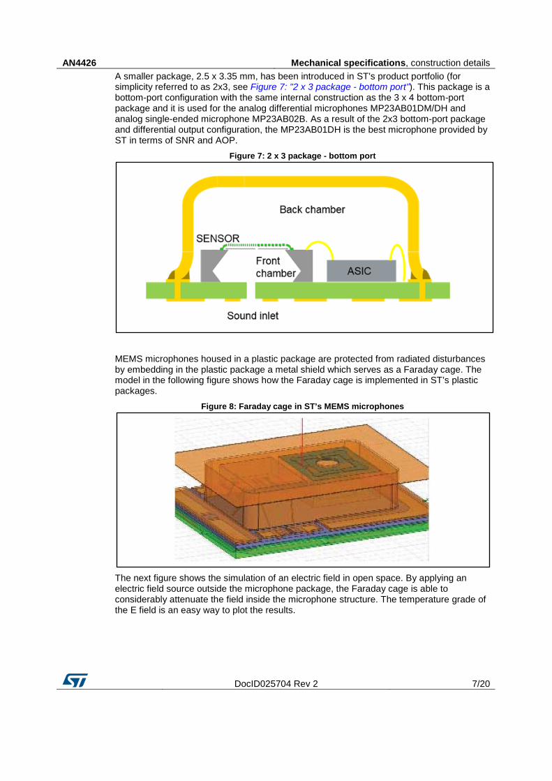
The 3x4 top-port configuration is basically a mirrored bottom-port microphone. The ASIC and the sensor are placed close to each other, the sensor is still under the sound inlet but these two components are attached to the top of the structure, in other words, the ASIC and MEMS are fixed to the package lid, not to the substrate. The pads are on the substrate and thus on the bottom side of the microphone. This configuration, covered by ST patents, allows optimizing all the benefits of the bottom-port microphone in terms of acoustic performance (i.e. maximized SNR and flat band) and all the benefits related to the top-port configuration during the assembly process.
Figure 6: 3 x 4 package - top port
AN4426 Mechanical specifications, construction details
DocID025704 Rev 2 7/20
A smaller package, 2.5 x 3.35 mm, has been introduced in ST's product portfolio (for simplicity referred to as 2x3, see Figure 7: "2 x 3 package - bottom port"). This package is a bottom-port configuration with the same internal construction as the 3 x 4 bottom-port package and it is used for the analog differential microphones MP23AB01DM/DH and analog single-ended microphone MP23AB02B. As a result of the 2x3 bottom-port package and differential output configuration, the MP23AB01DH is the best microphone provided by ST in terms of SNR and AOP.
Figure 7: 2 x 3 package - bottom port
MEMS microphones housed in a plastic package are protected from radiated disturbances by embedding in the plastic package a metal shield which serves as a Faraday cage. The model in the following figure shows how the Faraday cage is implemented in ST’s plastic packages.
Figure 8: Faraday cage in ST’s MEMS microphones
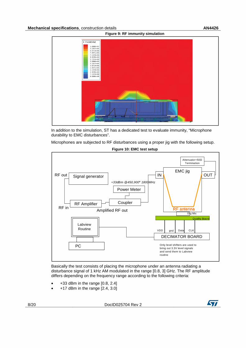
The next figure shows the simulation of an electric field in open space. By applying an electric field source outside the microphone package, the Faraday cage is able to considerably attenuate the field inside the microphone structure. The temperature grade of the E field is an easy way to plot the results.
Mechanical specifications, construction details AN4426
8/20 DocID025704 Rev 2
Figure 9: RF immunity simulation
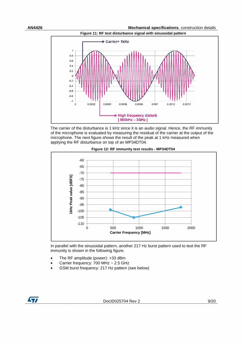
In addition to the simulation, ST has a dedicated test to evaluate immunity, “Microphone durability to EMC disturbances”.
Microphones are subjected to RF disturbances using a proper jig with the following setup. Figure 10: EMC test setup
Basically the test consists of placing the microphone under an antenna radiating a disturbance signal of 1 kHz AM modulated in the range [0.8, 3] GHz. The RF amplitude differs depending on the frequency range according to the following criteria:
• +33 dBm in the range [0.8, 2.4] • +17 dBm in the range [2.4, 3.0]
Signal generator
RF Amplifier
EMC jigIN OUTRF out
RF in
+33dBm @450,900° 1800MHz
RF antennaDig Mic
Quality Boa rd
VDD gnd Data CLK
DECIMATOR BOARD
PC
Attenuator+50ΩTermination
Amplified RF out
LabviewRoutine
Power Meter
Coupler
bring out 3.3V level signalsand send them to Labviewroutine
°
RF antenna
Quality Boa rd
Only level shifters are used to
AN4426 Mechanical specifications, construction details
DocID025704 Rev 2 9/20
Figure 11: RF test disturbance signal with sinusoidal pattern
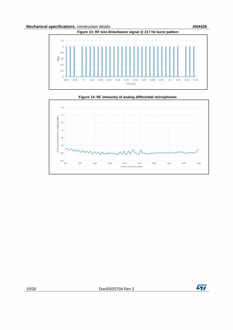
The carrier of the disturbance is 1 kHz since it is an audio signal. Hence, the RF immunity of the microphone is evaluated by measuring the residual of the carrier at the output of the microphone. The next figure shows the result of the peak at 1 kHz measured when applying the RF disturbance on top of an MP34DT04.
Figure 12: RF immunity test results - MP34DT04
In parallel with the sinusoidal pattern, another 217 Hz burst pattern used to test the RF immunity is shown in the following figure.
• The RF amplitude (power): +33 dBm • Carrier frequency: 700 MHz ~ 2.5 GHz • GSM burst frequency: 217 Hz pattern (see below)
-110
-105
-100
-95
-90
-85
-80
-75
-70
-65
-60
0 500 1000 1500 2000
1kH
zPe
akva
lue
[dB
FS]
Carrier Frequency [MHz]
Mechanical specifications, construction details AN4426
10/20 DocID025704 Rev 2
Figure 13: RF test disturbance signal @ 217 Hz burst pattern
Figure 14: RF immunity of analog differential microphones
AN4426 Acoustic parameters
DocID025704 Rev 2 11/20
2 Acoustic parameters
2.1 Sensitivity The sensitivity is the electrical signal at the microphone output to a given acoustic pressure as input. The reference of acoustic pressure is 1 Pa or 94 dBSPL @ 1 kHz. The sound pressure level, expressed in decibel, dBSPL=20*Log(P/Po) where Po = 20 µPa is the threshold of hearing. 20*Log(1Pa/20µPa) = 94 dBSPL
• For analog microphones the sensitivity is expressed in mVRMS/Pa or dBV/Pa • For digital microphones the sensitivity is expressed in dBFS
dBV ≠ dBFS. It is not correct to compare different units. As given in the above equations, dBV is in reference to 1VRMS instead of dBFS where the reference is the digital full scale.
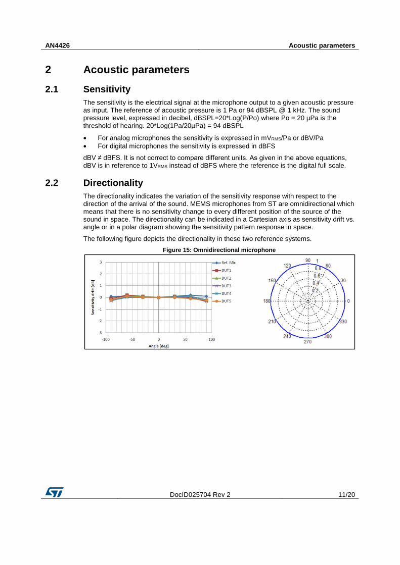
2.2 Directionality The directionality indicates the variation of the sensitivity response with respect to the direction of the arrival of the sound. MEMS microphones from ST are omnidirectional which means that there is no sensitivity change to every different position of the source of the sound in space. The directionality can be indicated in a Cartesian axis as sensitivity drift vs. angle or in a polar diagram showing the sensitivity pattern response in space.
The following figure depicts the directionality in these two reference systems. Figure 15: Omnidirectional microphone
Acoustic parameters AN4426
12/20 DocID025704 Rev 2
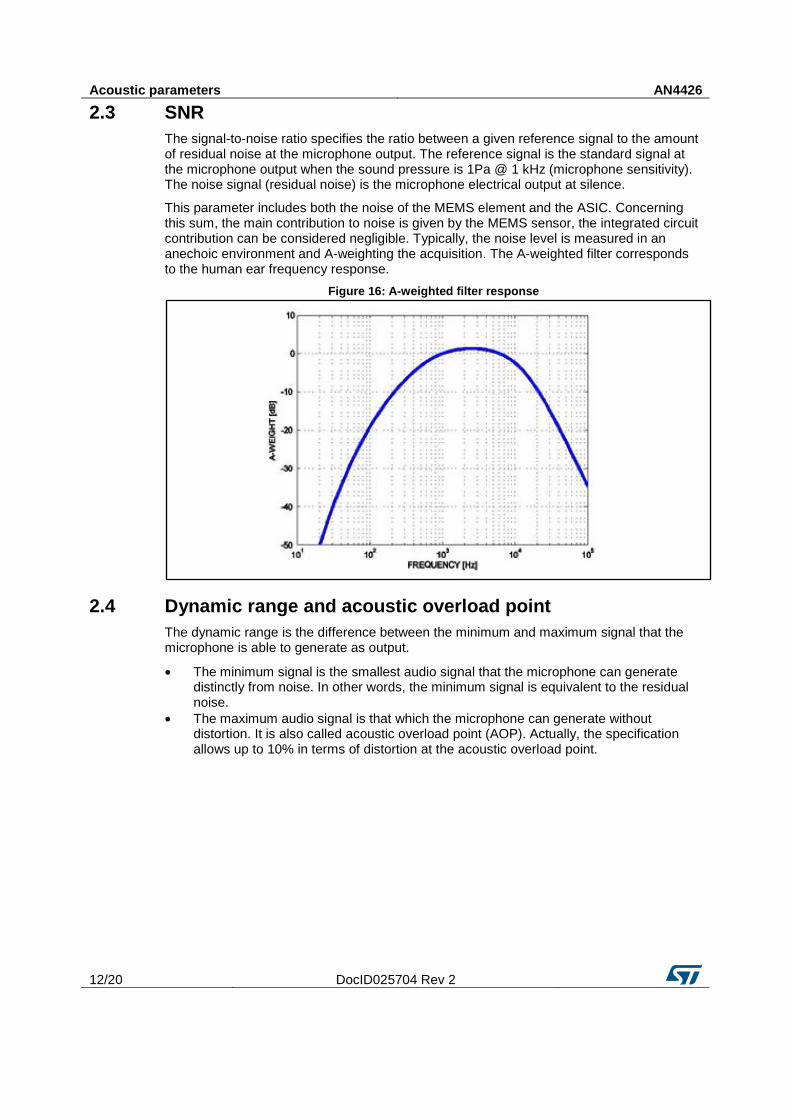
2.3 SNR The signal-to-noise ratio specifies the ratio between a given reference signal to the amount of residual noise at the microphone output. The reference signal is the standard signal at the microphone output when the sound pressure is 1Pa @ 1 kHz (microphone sensitivity). The noise signal (residual noise) is the microphone electrical output at silence.
This parameter includes both the noise of the MEMS element and the ASIC. Concerning this sum, the main contribution to noise is given by the MEMS sensor, the integrated circuit contribution can be considered negligible. Typically, the noise level is measured in an anechoic environment and A-weighting the acquisition. The A-weighted filter corresponds to the human ear frequency response.
Figure 16: A-weighted filter response
2.4 Dynamic range and acoustic overload point The dynamic range is the difference between the minimum and maximum signal that the microphone is able to generate as output.
• The minimum signal is the smallest audio signal that the microphone can generate distinctly from noise. In other words, the minimum signal is equivalent to the residual noise.
• The maximum audio signal is that which the microphone can generate without distortion. It is also called acoustic overload point (AOP). Actually, the specification allows up to 10% in terms of distortion at the acoustic overload point.
AN4426 Acoustic parameters
DocID025704 Rev 2 13/20
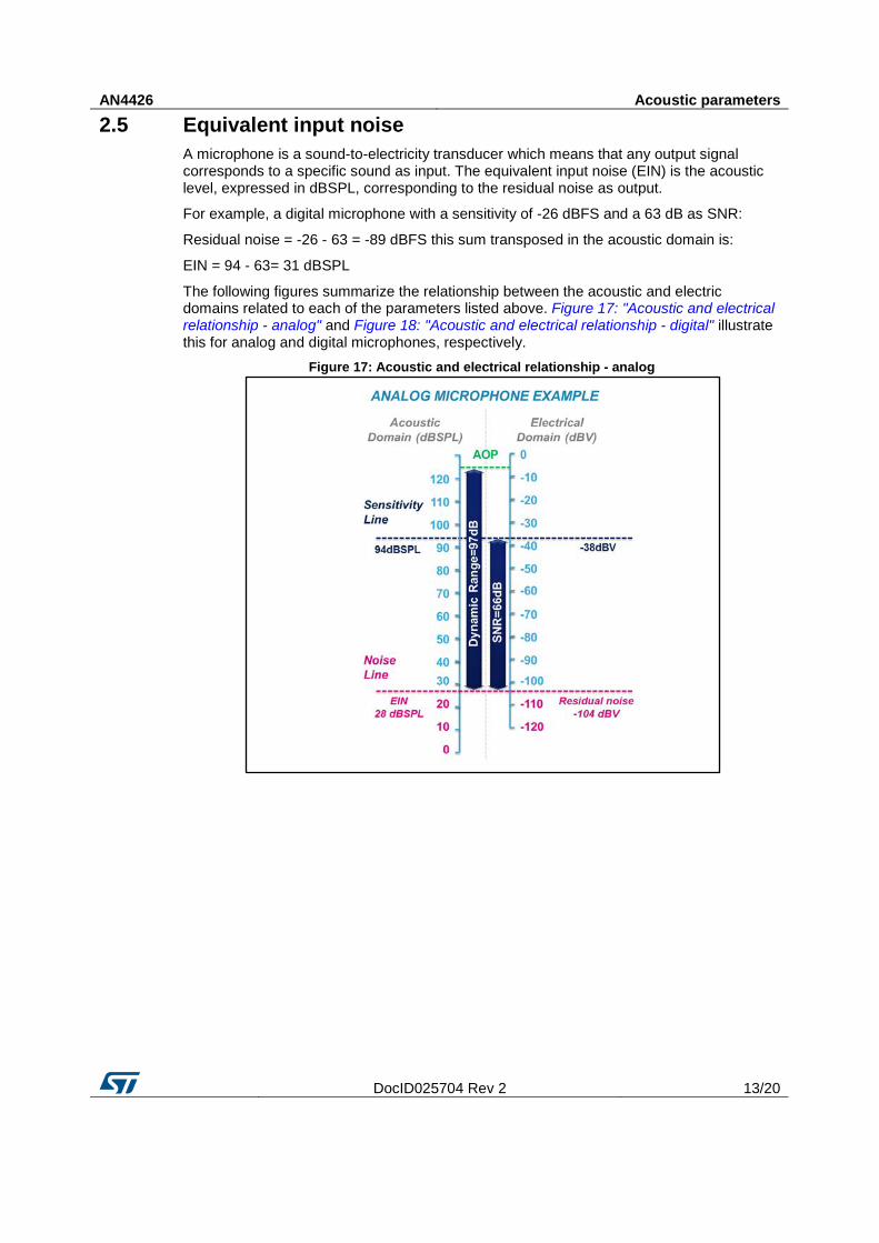
2.5 Equivalent input noise A microphone is a sound-to-electricity transducer which means that any output signal corresponds to a specific sound as input. The equivalent input noise (EIN) is the acoustic level, expressed in dBSPL, corresponding to the residual noise as output.
For example, a digital microphone with a sensitivity of -26 dBFS and a 63 dB as SNR:
Residual noise = -26 - 63 = -89 dBFS this sum transposed in the acoustic domain is:
EIN = 94 - 63= 31 dBSPL
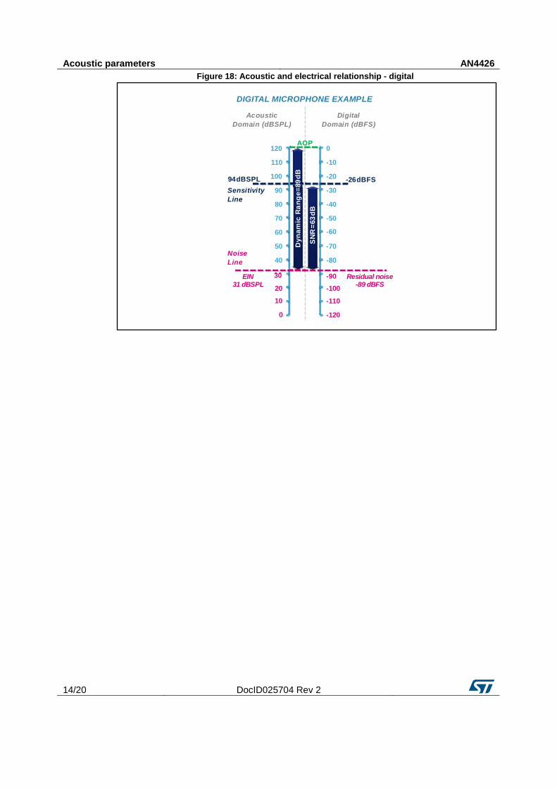
The following figures summarize the relationship between the acoustic and electric domains related to each of the parameters listed above. Figure 17: "Acoustic and electrical relationship - analog" and Figure 18: "Acoustic and electrical relationship - digital" illustrate this for analog and digital microphones, respectively.
Figure 17: Acoustic and electrical relationship - analog
Acoustic parameters AN4426
14/20 DocID025704 Rev 2
Figure 18: Acoustic and electrical relationship - digital
120
110
100
90
70
80
50
60
40
30
20
10
0 -120
-110
-100-90
-70
-80
-50
-60
-40
-30
-20
-10
0
94dBSPL
AOP
SN
R=6
3dB
-26dBFS
Dyn
amic
Ran
ge=8
9 dB
AcousticDomain (dBSPL)
DigitalDomain (dBFS)
SensitivityLine
NoiseLine
DIGITAL MICROPHONE EXAMPLE
EIN31 dBSPL
Residual noise-89 dBFS
AN4426 Acoustic parameters
DocID025704 Rev 2 15/20
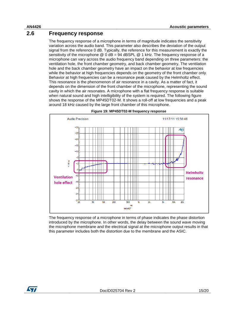
2.6 Frequency response The frequency response of a microphone in terms of magnitude indicates the sensitivity variation across the audio band. This parameter also describes the deviation of the output signal from the reference 0 dB. Typically, the reference for this measurement is exactly the sensitivity of the microphone @ 0 dB = 94 dBSPL @ 1 kHz. The frequency response of a microphone can vary across the audio frequency band depending on three parameters: the ventilation hole, the front chamber geometry, and back chamber geometry. The ventilation hole and the back chamber geometry have an impact on the behavior at low frequencies while the behavior at high frequencies depends on the geometry of the front chamber only. Behavior at high frequencies can be a resonance peak caused by the Helmholtz effect. This resonance is the phenomenon of air resonance in a cavity. As a matter of fact, it depends on the dimension of the front chamber of the microphone, representing the sound cavity in which the air resonates. A microphone with a flat frequency response is suitable when natural sound and high intelligibility of the system is required. The following figure shows the response of the MP45DT02-M. It shows a roll-off at low frequencies and a peak around 18 kHz caused by the large front chamber of this microphone.
Figure 19: MP45DT02-M frequency response
The frequency response of a microphone in terms of phase indicates the phase distortion introduced by the microphone. In other words, the delay between the sound wave moving the microphone membrane and the electrical signal at the microphone output results in that this parameter includes both the distortion due to the membrane and the ASIC.
Acoustic parameters AN4426
16/20 DocID025704 Rev 2
2.7 Total harmonic distortion THD is the measurement of the distortion affecting the electrical output signal of the microphone given an undistorted acoustic signal as input. THD+N is expressed as a ratio of the integer in a specified band of the power of the harmonics plus the power of noise and the power of the undistorted signal (fundamental).
Equation 1
𝑇𝑇𝑇𝑇𝑇𝑇 + 𝑁𝑁(%) =∑ 𝑃𝑃𝑃𝑃𝑃𝑃𝑃𝑃𝑃𝑃(𝑇𝑇𝐻𝐻𝑃𝑃𝐻𝐻𝑃𝑃𝐻𝐻𝐻𝐻𝐻𝐻𝐻𝐻) + 𝑃𝑃𝑃𝑃𝑃𝑃𝑃𝑃𝑃𝑃(𝑁𝑁𝑃𝑃𝐻𝐻𝐻𝐻𝑃𝑃)𝑁𝑁𝑛𝑛−1
𝑃𝑃𝑃𝑃𝑃𝑃𝑃𝑃𝑃𝑃(𝐹𝐹𝐹𝐹𝐻𝐻𝐹𝐹𝐻𝐻𝐻𝐻𝑃𝑃𝐻𝐻𝐹𝐹𝐻𝐻𝐹𝐹)
Typically ST indicates the THD+N measured in the (50 Hz - 4 kHz) band for a given undistorted signal 1 kHz @ 100 dBSPL.
2.8 PSRR and PSR PSRR indicates the capability of the ASIC to reject noise added to the supply voltage. To evaluate this parameter, a tone of VIN = 100 mVpk-pk @ 217 Hz (GSM switching frequency in phone applications) is added to the power supply and then the amplitude of the output is measured. The added noise can be either a square wave or sinusoidal wave. Typically the square wave is preferred since it is the worst case.
PSRR is the ratio of the residual noise amplitude at the microphone output (VOUT @ 217 Hz) to the added spurious signal on the supply voltage. It is typically expressed in dB as given in the equation below:
Equation 2
𝑃𝑃𝑃𝑃𝑃𝑃𝑃𝑃 = 20 𝑥𝑥 log (𝑉𝑉𝑂𝑂𝑂𝑂𝑂𝑂@217𝑇𝑇𝐻𝐻)(𝑉𝑉𝐼𝐼𝑁𝑁@217𝑇𝑇𝐻𝐻)
The capability of the integrated circuit to reject noise added to the supply voltage can also be expressed with another parameter that is the PSR. Basically it is simply a measurement of the output when noise of 100 mVpk-pk @ 217 Hz is superposed to the supply voltage. Consequently expressed in dB as given in the equation below:
Equation 3
𝑃𝑃𝑃𝑃𝑃𝑃 = 20 𝑥𝑥 log[𝑉𝑉𝑂𝑂𝑂𝑂𝑂𝑂@ 217𝑇𝑇𝐻𝐻]
To evaluate either the PSRR or PSR, proper sealing of the sound inlet or measurements performed in an anechoic chamber are recommended to avoid mixing the superimposed noise with that of the noise floor of the output. Finally, in the microphone datasheets PSR is commonly given instead of PSRR.
AN4426 MEMS microphone portfolio
DocID025704 Rev 2 17/20
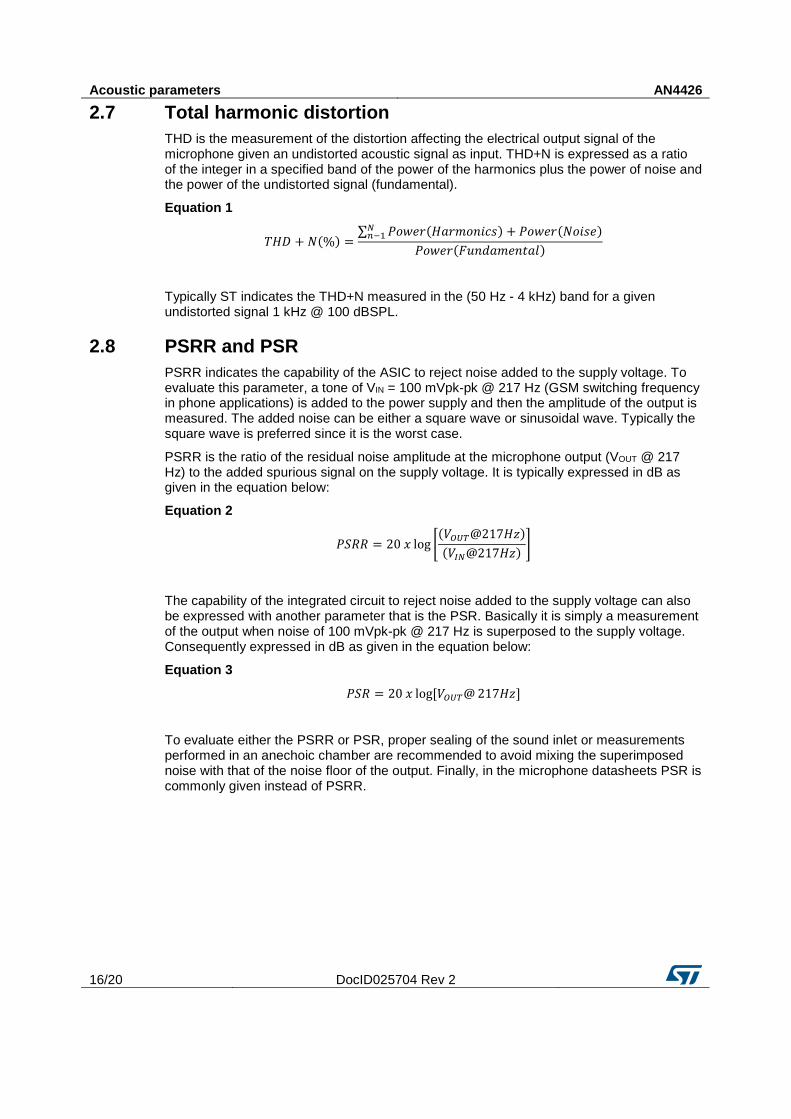
3 MEMS microphone portfolio Figure 20: MEMS microphone portfolio
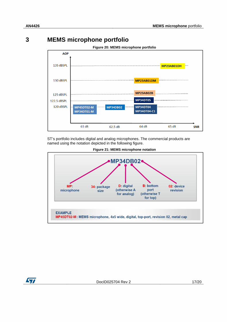
ST’s portfolio includes digital and analog microphones. The commercial products are named using the notation depicted in the following figure.
Figure 21: MEMS microphone notation
MEMS microphone portfolio AN4426
18/20 DocID025704 Rev 2
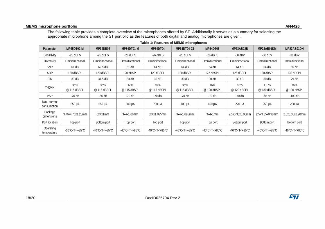
The following table provides a complete overview of the microphones offered by ST. Additionally it serves as a summary for selecting the appropriate microphone among the ST portfolio as the features of both digital and analog microphones are given.
Table 1: Features of MEMS microphones Parameter MP45DT02-M MP34DB02 MP34DT01-M MP34DT04 MP34DT04-C1 MP34DT05 MP23AB02B MP23AB01DM MP23AB01DH
Sensitivity -26 dBFS -26 dBFS -26 dBFS -26 dBFS -26 dBFS -26 dBFS -38 dBV -38 dBV -38 dBV
Directivity Omnidirectional Omnidirectional Omnidirectional Omnidirectional Omnidirectional Omnidirectional Omnidirectional Omnidirectional Omnidirectional
SNR 61 dB 62.5 dB 61 dB 64 dB 64 dB 64 dB 64 dB 64 dB 65 dB
AOP 120 dBSPL 120 dBSPL 120 dBSPL 120 dBSPL 120 dBSPL 122 dBSPL 125 dBSPL 130 dBSPL 135 dBSPL
EIN 33 dB 31.5 dB 33 dB 30 dB 30 dB 30 dB 30 dB 30 dB 29 dB
THD+N <5%
@ 115 dBSPL <5%
@ 115 dBSPL <2%
@ 115 dBSPL <5%
@ 115 dBSPL <5%
@ 115 dBSPL <6%
@ 120 dBSPL <2%
@ 120 dBSPL <10%
@ 130 dBSPL <5%
@ 130 dBSPL
PSR -70 dB -86 dB -70 dB -70 dB -70 dB -72 dB -70 dB -85 dB -100 dB
Max. current consumption 650 µA 650 µA 600 µA 700 µA 700 µA 650 µA 220 µA 250 µA 250 µA
Package dimensions 3.76x4.76x1.25mm 3x4x1mm 3x4x1.06mm 3x4x1.095mm 3x4x1.095mm 3x4x1mm 2.5x3.35x0.98mm 2.5x3.35x0.98mm 2.5x3.35x0.98mm
Port location Top port Bottom port Top port Top port Top port Top port Bottom port Bottom port Bottom port
Operating temperature -30°C<T<+85°C -40°C<T<+85°C -40°C<T<+85°C -40°C<T<+85°C -40°C<T<+85°C -40°C<T<+85°C -40°C<T<+85°C -40°C<T<+85°C -40°C<T<+85°C
AN4426 Revision history
DocID025704 Rev 2 19/20
4 Revision history Table 2: Document revision history
Date Revision Changes
09-Jan-2014 1 Initial release
14-Feb-2017 2
Updated part numbers throughout document Updated "Introduction" and Section 1: "Mechanical specifications, construction details" Updated Figure 5: "3 x 4 metal cap package - bottom port", Figure 20: "MEMS microphone portfolio", Figure 21: "MEMS microphone notation" Added Figure 7: "2 x 3 package - bottom port", Figure 13: "RF test disturbance signal @ 217 Hz burst pattern", Figure 14: "RF immunity of analog differential microphones" Updated Table 1: "Features of MEMS microphones"
AN4426
20/20 DocID025704 Rev 2
IMPORTANT NOTICE – PLEASE READ CAREFULLY
STMicroelectronics NV and its subsidiaries (“ST”) reserve the right to make changes, corrections, enhancements, modifications, and improvements to ST products and/or to this document at any time without notice. Purchasers should obtain the latest relevant information on ST products before placing orders. ST products are sold pursuant to ST’s terms and conditions of sale in place at the time of order acknowledgement.
Purchasers are solely responsible for the choice, selection, and use of ST products and ST assumes no liability for application assistance or the design of Purchasers’ products.
No license, express or implied, to any intellectual property right is granted by ST herein.
Resale of ST products with provisions different from the information set forth herein shall void any warranty granted by ST for such product.
ST and the ST logo are trademarks of ST. All other product or service names are the property of their respective owners.
Information in this document supersedes and replaces information previously supplied in any prior versions of this document.
© 2017 STMicroelectronics – All rights reserved