tut sopc introduction vhdl - Georgia Institute of...
20
Introduction to the Altera SOPC Builder Using VHDL Design This tutorial presents an introduction to Altera’s SOPC Builder software, which is used to implement a system that uses the Nios II processor on an Altera FPGA device. The system development flow is illustrated by giving step-by-step instructions for using the SOPC Builder in conjuction with the Quartus R II software to implement a simple system. The last step in the development process involves configuring the designed circuit in an actual FPGA device, and running an application program. To show how this is done, it is assumed that the user has access to the Altera DE2 Development and Education board connected to a computer that has Quartus II and Nios R II software installed. The screen captures in the tutorial were obtained using the Quartus II version 5.1; if other versions of the software are used, some of the images may be slightly different. Contents: Nios II System Altera’s SOPC Builder Integration of the Nios II System into a Quartus II Project Running the Application Program 1
-
Upload
nguyenthuan -
Category
Documents
-
view
231 -
download
8
Transcript of tut sopc introduction vhdl - Georgia Institute of...
Introduction to the Altera SOPC BuilderUsing VHDL Design
This tutorial presents an introduction to Altera’s SOPC Builder software, which is used to implement a systemthat uses the Nios II processor on an Altera FPGA device. The system development flow is illustrated by givingstep-by-step instructions for using the SOPC Builder in conjuction with the QuartusR© II software to implement asimple system.
The last step in the development process involves configuring the designed circuit in an actual FPGA device,and running an application program. To show how this is done,it is assumed that the user has access to the AlteraDE2 Development and Education board connected to a computerthat has Quartus II and NiosR© II softwareinstalled.
The screen captures in the tutorial were obtained using the Quartus II version 5.1; if other versions of thesoftware are used, some of the images may be slightly different.
Contents:Nios II SystemAltera’s SOPC BuilderIntegration of the Nios II System into a Quartus II ProjectRunning the Application Program
1
Altera’s Nios II is a soft processor, defined in a hardware description language, which can be implementedin Altera’s FPGA devices by using the QuartusR© II CAD system. To implement a useful system it is necessaryto add other funcional units such as memories, input/outputinterfaces, timers, and communications interfaces.To facilitate the implementation of such systems, it is useful to have computer-aided-design (CAD) software forimplementing a system-on-a-programmable-chip (SOPC). Altera’s SOPC Builder is the software needed for thistask.
This tutorial provides a basic introduction to Altera’s SOPC Builder, which will allow the reader to quicklyimplement a simple Nios II system on the Altera DE2 board. Fora fuller treatment of the SOPC Builder, thereader can consult theNios II Hardware Development Tutorial. A complete description of the SOPC Builder canbe found in theQuartus II Handbook Volume 4: SOPC Builder. These documents are available on the Altera website.
1 Nios II System
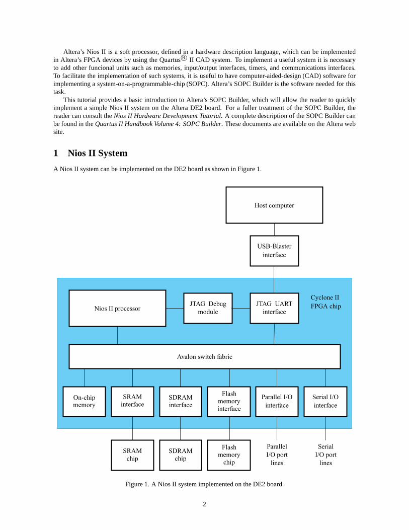
A Nios II system can be implemented on the DE2 board as shown inFigure 1.
On-chipmemory
interface
SDRAMinterface
Flashmemory
Parallel I/O
interface
Serial I/O
interface
SRAMinterface
SRAM
chip
SDRAMchip
chip
Flashmemory
Avalon switch fabric
Nios II processorJTAG UART
interface
USB-Blaster
interface
Host computer
lines
Parallel
I/O port
lines
Serial
I/O port
Cyclone II
FPGA chipJTAG Debug
module
Figure 1. A Nios II system implemented on the DE2 board.
2
The Nios II processor and the interfaces needed to connect toother chips on the DE2 board are implementedin the Cyclone II FPGA chip. These components are interconnected by means of the interconnection networkcalled the Avalon Switch Fabric. The memory blocks in the Cyclone II device can be used to provide an on-chipmemory for the Nios II processor. The SRAM, SDRAM and Flash memory chips on the DE2 board are accessedthrough the appropriate interfaces. Parallel and serial input/output interfaces provide typical I/O ports used incomputer systems. A special JTAG UART interface is used to connect to the circuitry that provides a UniversalSerial Bus (USB) link to the host computer to which the DE2 board is connected. This circuitry and the associatedsoftware is called theUSB-Blaster. Another module, called the JTAG Debug module, is provided to allow the hostcomputer to control the Nios II system. It makes it possible to perform operations such as downloading programsinto memory, starting and stopping execution, setting breakpoints, and collecting real-time execution trace data.
Since all parts of the Nios II system implemented on the FPGA chip are defined by using a hardware descrip-tion language, a knowledgeable user could write such code toimplement any part of the system. This would bean onnerous and time consuming task. Instead, one can use theSOPC Builder to implement a desired systemsimply by choosing the required components and specifying the parameters needed to make each component fitthe overall requirements of the system. In this tutorial, wewill illustrate the capability of the SOPC Builder bydesigning a very simple system. The same approach is used to design large systems.
On-chipmemory
parallel input
interface
parallel output
interface
Avalon switch fabric
Nios II processorJTAG UART
interface
USB-Blaster
interface
Host computer
Cyclone II
FPGA chip
SW7 SW0 LEDG7 LEDG0
Reset_n Clock
LEDs
JTAG Debug
module
Switches
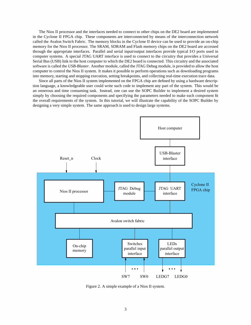
Figure 2. A simple example of a Nios II system.
3
Our example system is given in Figure 2. The system realizes atrivial task. Eight toggle switches on the DE2board,SW7− 0, are used to turn on or off the eight green LEDs,LEDG7− 0. The switches are connected to theNios II system by means of a parallel I/O interface configuredto act as an input port. The LEDs are driven by thesignals from another parallel I/O interface configured to act as an output port. To achieve the desired operation, theeight-bit pattern corresponding to the state of the switches has to be sent to the output port to activate the LEDs.This will be done by having the Nios II processor execute a program stored in the on-chip memory. Continuousoperation is required, such that as the switches are toggledthe lights change accordingly.
We will use the SOPC Builder to design the hardware depicted in Figure 2. Next, we will assign the Cyclone IIpins to realize the connections between the parallel interfaces and the switches and LEDs which act as I/O devices.Then, we will configure the FPGA to implement the designed system. Finally, we will use the software tool calledtheNios II Debug Clientto assemble, download and execute a Nios II program that performs the desired task.
Doing this tutorial, the reader will learn about:
• Using the SOPC Builder to design a Nios II-based system
• Integrating the designed Nios II system into a Quartus II project
• Implementing the designed system on the DE2 board
• Running an application program on the Nios II processor
2 Altera’s SOPC Builder
The SOPC Builder is a tool used in conjuction with the QuartusII CAD software. It allows the user to easilycreate a system based on the Nios II processor, by simply selecting the desired functional units and specifyingtheir parameters. To implement the system in Figure 2, we have to instantiate the following functional units:
• Nios II processor, which is referred to as a Central Processing Unit (CPU)
• On-chip memory, which consists of the memory blocks in the Cyclone II chip; we will specify a 4-Kbytememory arranged in 32-bit words
• Two parallel I/O interfaces
• JTAG UART interface for communication with the host computer
To define the desired system, start the Quartus II software and perform the following steps:
1. Create a new Quartus II project for your system. As shown inFigure 3, we stored our project in a directorycalledsopc_builder_tutorial, and we assigned the namelights to both the project and its top-level designentity. You can choose a different directory or project name, but be aware that the SOPC Builder softwaredoes not permit the use of spaces in file names. For example, anattempt to use a directory namesopcbuilder tutorialwould lead to an error. In your project, choose the EP2C35F672C6 chip as the target device,because this is the FPGA on the DE2 board.
2. SelectTools > SOPC Builder, which leads to the pop-up box in Figure 4. Enternios_systemas the systemname; this will be the name of the system that the SOPC Builderwill generate. Choose VHDL as the targetHDL, in which the system module will be specified. ClickOK to reach the window in Figure 5.
4
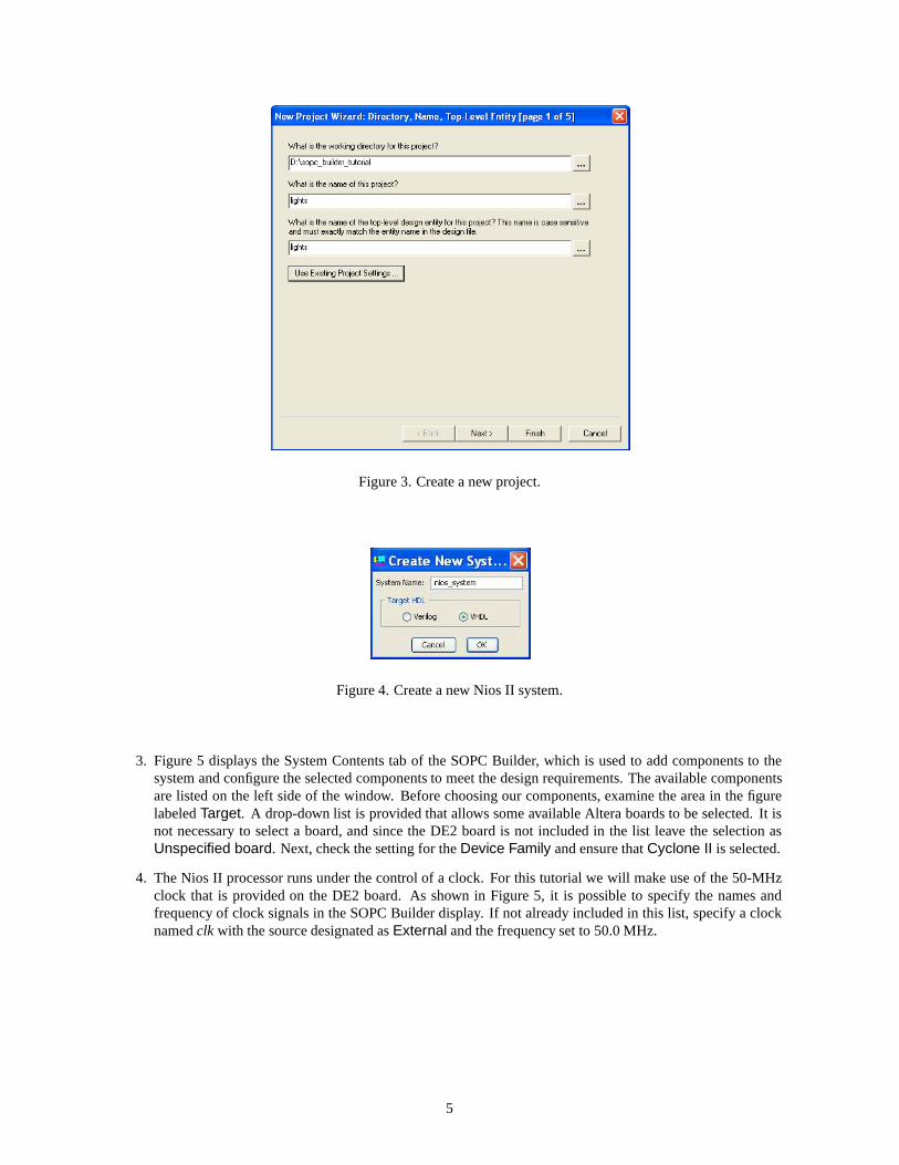
Figure 3. Create a new project.
Figure 4. Create a new Nios II system.
3. Figure 5 displays the System Contents tab of the SOPC Builder, which is used to add components to thesystem and configure the selected components to meet the design requirements. The available componentsare listed on the left side of the window. Before choosing ourcomponents, examine the area in the figurelabeledTarget. A drop-down list is provided that allows some available Altera boards to be selected. It isnot necessary to select a board, and since the DE2 board is notincluded in the list leave the selection asUnspecified board. Next, check the setting for theDevice Family and ensure thatCyclone II is selected.
4. The Nios II processor runs under the control of a clock. Forthis tutorial we will make use of the 50-MHzclock that is provided on the DE2 board. As shown in Figure 5, it is possible to specify the names andfrequency of clock signals in the SOPC Builder display. If not already included in this list, specify a clocknamedclk with the source designated asExternal and the frequency set to 50.0 MHz.
5
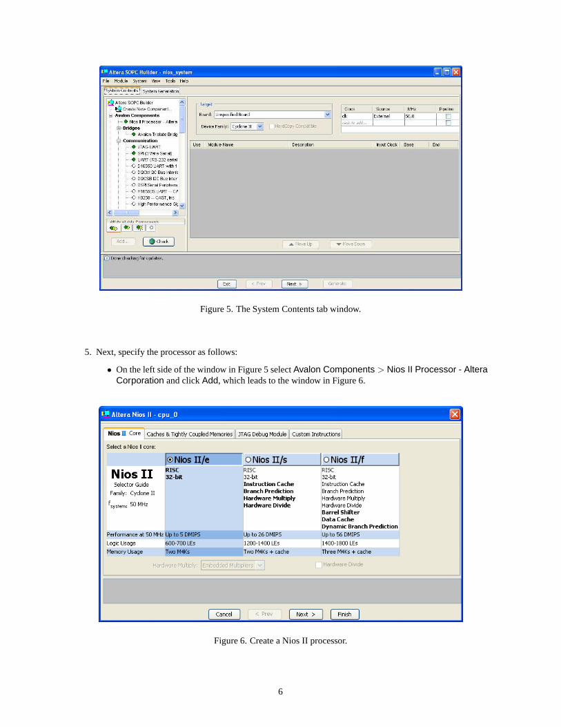
Figure 5. The System Contents tab window.
5. Next, specify the processor as follows:
• On the left side of the window in Figure 5 selectAvalon Components > Nios II Processor - AlteraCorporation and clickAdd, which leads to the window in Figure 6.
Figure 6. Create a Nios II processor.
6
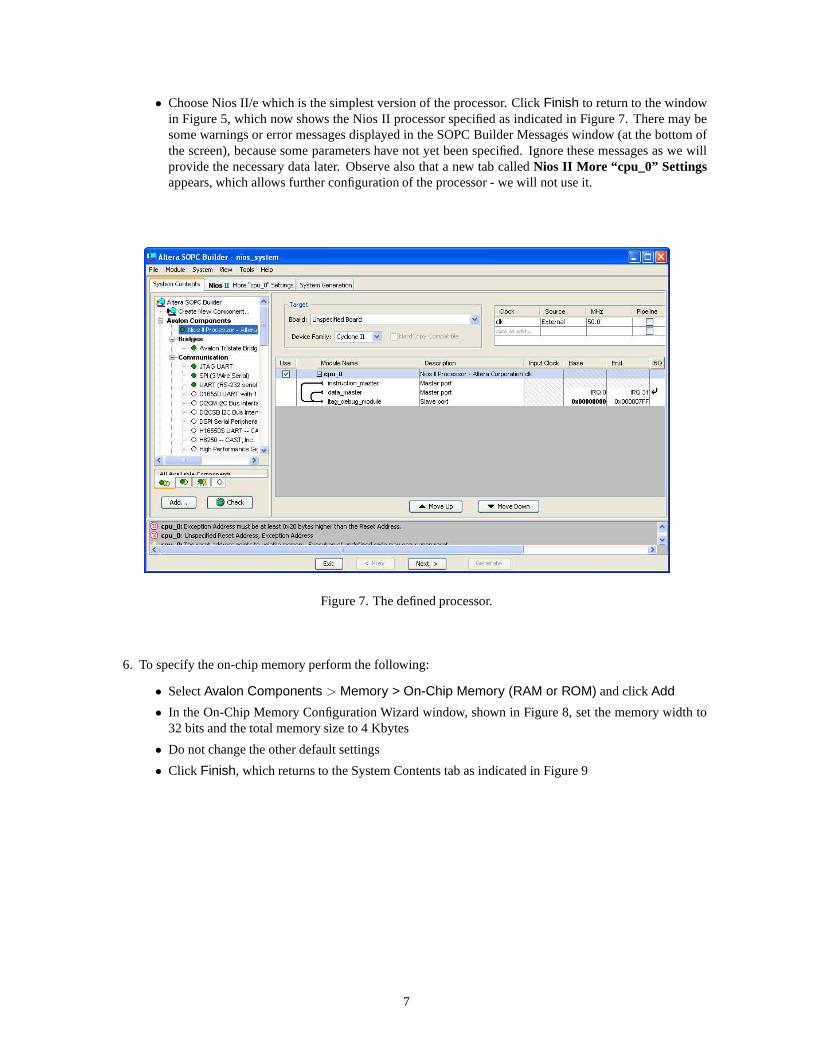
• Choose Nios II/e which is the simplest version of the processor. Click Finish to return to the windowin Figure 5, which now shows the Nios II processor specified asindicated in Figure 7. There may besome warnings or error messages displayed in the SOPC Builder Messages window (at the bottom ofthe screen), because some parameters have not yet been specified. Ignore these messages as we willprovide the necessary data later. Observe also that a new tabcalledNios II More “cpu_0” Settingsappears, which allows further configuration of the processor - we will not use it.
Figure 7. The defined processor.
6. To specify the on-chip memory perform the following:
• SelectAvalon Components > Memory > On-Chip Memory (RAM or ROM) and clickAdd
• In the On-Chip Memory Configuration Wizard window, shown in Figure 8, set the memory width to32 bits and the total memory size to 4 Kbytes
• Do not change the other default settings
• Click Finish, which returns to the System Contents tab as indicated in Figure 9
7
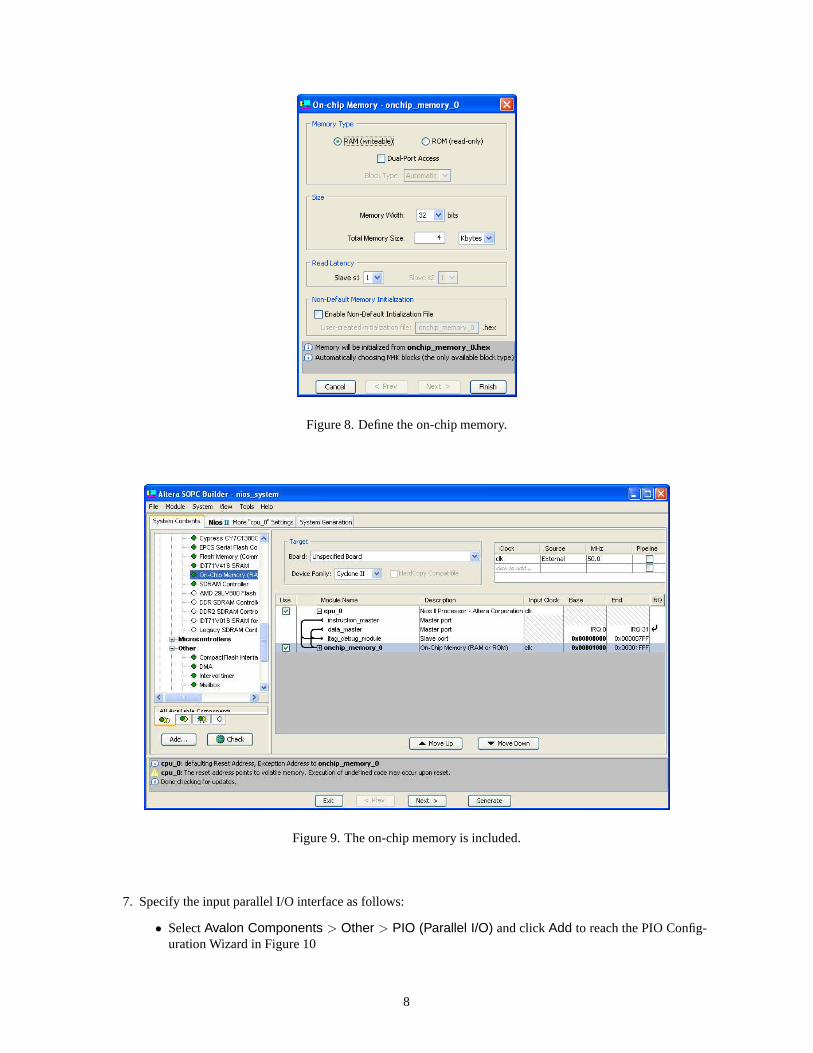
Figure 8. Define the on-chip memory.
Figure 9. The on-chip memory is included.
7. Specify the input parallel I/O interface as follows:
• SelectAvalon Components > Other > PIO (Parallel I/O) and clickAdd to reach the PIO Config-uration Wizard in Figure 10
8
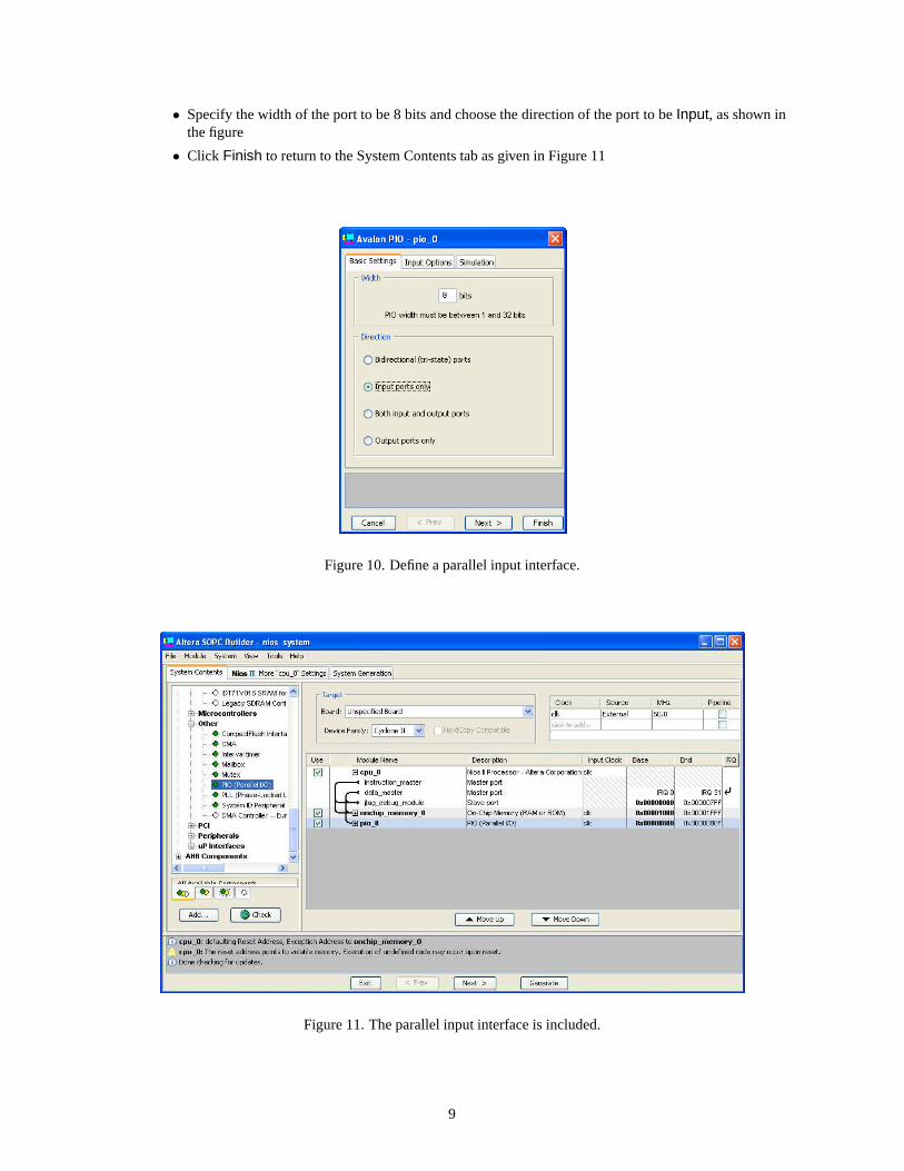
• Specify the width of the port to be 8 bits and choose the direction of the port to beInput, as shown inthe figure
• Click Finish to return to the System Contents tab as given in Figure 11
Figure 10. Define a parallel input interface.
Figure 11. The parallel input interface is included.
9

8. In the same way, specify the output parallel I/O interface:
• SelectAvalon Components > Other > PIO (Parallel I/O) and clickAdd to reach the PIO Config-uration Wizard again
• Specify the width of the port to be 8 bits and choose the direction of the port to beOutput
• Click Finish to return to the System Contents tab
9. We wish to connect to a host computer and provide a means forcommunication between the Nios II systemand the host computer. This can be accomplished by instantiating the JTAG UART interface as follows:
• SelectAvalon Components > Communication > JTAG UART and clickAdd to reach the JTAGUART Configuration Wizard in Figure 12
• Do not change the default settings
• Click Finish to return to the System Contents tab
Figure 12. Define the JTAG UART interface.
10. The complete system is depicted in Figure 13. Note that the SOPC Builder automatically chooses names forthe various components. The names are not necessarily descriptive enough to be easily associated with thetarget design, but they can be changed. In Figure 2, we use thenames Switches and LEDs for the parallelinput and output interfaces, respectively. These names canbe used in the implemented system. Right-clickon thepio_0 name and then selectRename. Change the name to Switches. Similarly, changepio_1 toLEDs.
11. The base and end addresses of the various components in the designed system can be assigned by the user,but they can also be assigned automatically by the SOPC Builder. We will choose the latter possibility. So,select the command (using the menus at the top of the SOPC Builder window)System > Auto-AssignBase Addresses, which produces the assignment shown in Figure 14.
10
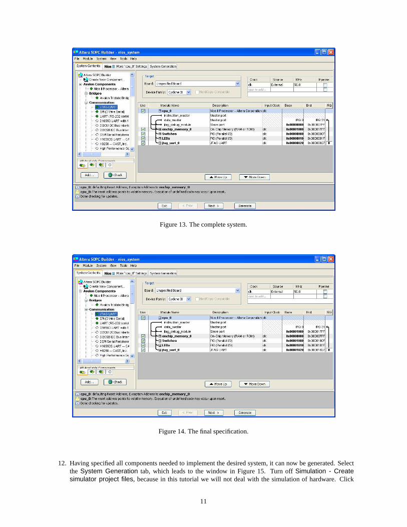
Figure 13. The complete system.
Figure 14. The final specification.
12. Having specified all components needed to implement the desired system, it can now be generated. Selectthe System Generation tab, which leads to the window in Figure 15. Turn offSimulation - Createsimulator project files, because in this tutorial we will not deal with the simulation of hardware. Click
11
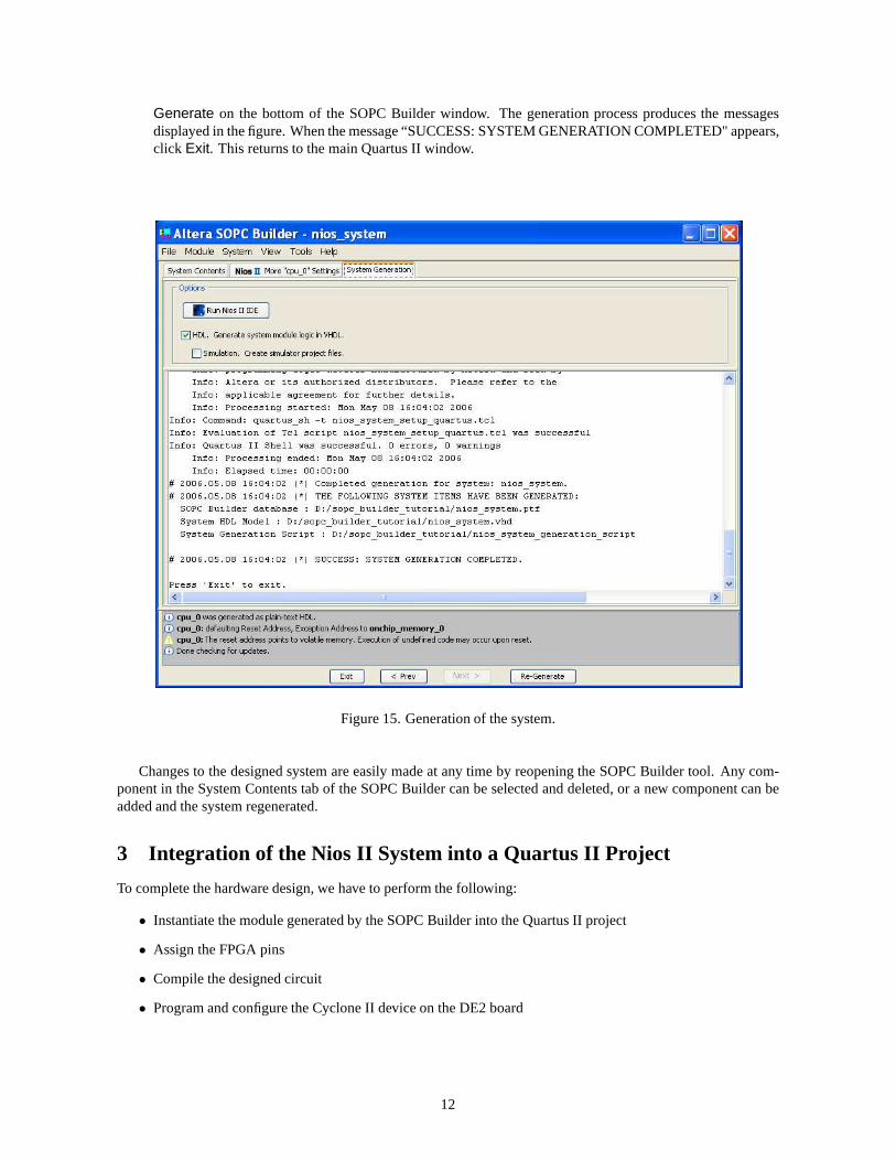
Generate on the bottom of the SOPC Builder window. The generation process produces the messagesdisplayed in the figure. When the message “SUCCESS: SYSTEM GENERATION COMPLETED" appears,click Exit. This returns to the main Quartus II window.
Figure 15. Generation of the system.
Changes to the designed system are easily made at any time by reopening the SOPC Builder tool. Any com-ponent in the System Contents tab of the SOPC Builder can be selected and deleted, or a new component can beadded and the system regenerated.
3 Integration of the Nios II System into a Quartus II Project
To complete the hardware design, we have to perform the following:
• Instantiate the module generated by the SOPC Builder into the Quartus II project
• Assign the FPGA pins
• Compile the designed circuit
• Program and configure the Cyclone II device on the DE2 board
12
3.1 Instantiation of the Module Generated by the SOPC Builder
The instantiation of the generated module depends on the design entry method chosen for the overall Quartus IIproject. We have chosen to use VHDL, but the approach is similar for both Verilog and schematic entry methods.
Normally, the Nios II module is likely to be a part of a larger design. However, in the case of our simpleexample there is no other circuitry needed. All we need to do is instantiate the Nios II system in our top-levelVHDL file, and connect inputs and outputs of the parallel I/O ports, as well as the clock and reset inputs, to theappropriate pins on the Cyclone II device.
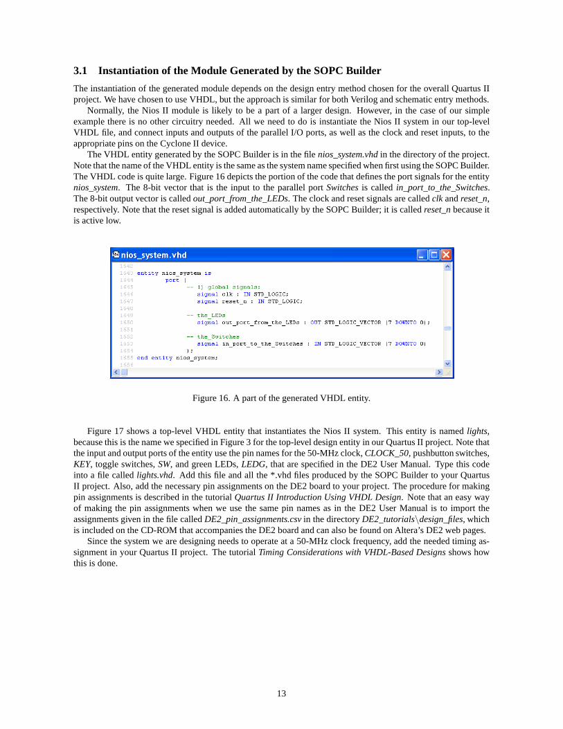
The VHDL entity generated by the SOPC Builder is in the filenios_system.vhdin the directory of the project.Note that the name of the VHDL entity is the same as the system name specified when first using the SOPC Builder.The VHDL code is quite large. Figure 16 depicts the portion ofthe code that defines the port signals for the entitynios_system. The 8-bit vector that is the input to the parallel portSwitchesis called in_port_to_the_Switches.The 8-bit output vector is calledout_port_from_the_LEDs. The clock and reset signals are calledclk andreset_n,respectively. Note that the reset signal is added automatically by the SOPC Builder; it is calledreset_nbecause itis active low.
Figure 16. A part of the generated VHDL entity.
Figure 17 shows a top-level VHDL entity that instantiates the Nios II system. This entity is namedlights,because this is the name we specified in Figure 3 for the top-level design entity in our Quartus II project. Note thatthe input and output ports of the entity use the pin names for the 50-MHz clock,CLOCK_50, pushbutton switches,KEY, toggle switches,SW, and green LEDs,LEDG, that are specified in the DE2 User Manual. Type this codeinto a file calledlights.vhd. Add this file and all the *.vhd files produced by the SOPC Builder to your QuartusII project. Also, add the necessary pin assignments on the DE2 board to your project. The procedure for makingpin assignments is described in the tutorialQuartus II Introduction Using VHDL Design. Note that an easy wayof making the pin assignments when we use the same pin names asin the DE2 User Manual is to import theassignments given in the file calledDE2_pin_assignments.csvin the directoryDE2_tutorials\design_files, whichis included on the CD-ROM that accompanies the DE2 board and can also be found on Altera’s DE2 web pages.
Since the system we are designing needs to operate at a 50-MHzclock frequency, add the needed timing as-signment in your Quartus II project. The tutorialTiming Considerations with VHDL-Based Designsshows howthis is done.
13
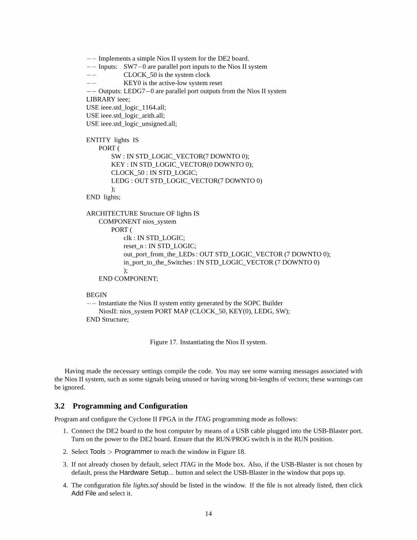
−− Implements a simple Nios II system for the DE2 board.−− Inputs: SW7−0 are parallel port inputs to the Nios II system−− CLOCK_50 is the system clock−− KEY0 is the active-low system reset−− Outputs: LEDG7−0 are parallel port outputs from the Nios II systemLIBRARY ieee;USE ieee.std_logic_1164.all;USE ieee.std_logic_arith.all;USE ieee.std_logic_unsigned.all;
ENTITY lights ISPORT (
SW : IN STD_LOGIC_VECTOR(7 DOWNTO 0);KEY : IN STD_LOGIC_VECTOR(0 DOWNTO 0);CLOCK_50 : IN STD_LOGIC;LEDG : OUT STD_LOGIC_VECTOR(7 DOWNTO 0));
END lights;
ARCHITECTURE Structure OF lights ISCOMPONENT nios_system
PORT (clk : IN STD_LOGIC;reset_n : IN STD_LOGIC;out_port_from_the_LEDs : OUT STD_LOGIC_VECTOR (7 DOWNTO 0);in_port_to_the_Switches : IN STD_LOGIC_VECTOR (7 DOWNTO 0));
END COMPONENT;
BEGIN−− Instantiate the Nios II system entity generated by the SOPC Builder
NiosII: nios_system PORT MAP (CLOCK_50, KEY(0), LEDG, SW);END Structure;
Figure 17. Instantiating the Nios II system.
Having made the necessary settings compile the code. You maysee some warning messages associated withthe Nios II system, such as some signals being unused or having wrong bit-lengths of vectors; these warnings canbe ignored.
3.2 Programming and Configuration
Program and configure the Cyclone II FPGA in the JTAG programming mode as follows:
1. Connect the DE2 board to the host computer by means of a USB cable plugged into the USB-Blaster port.Turn on the power to the DE2 board. Ensure that the RUN/PROG switch is in the RUN position.
2. SelectTools > Programmer to reach the window in Figure 18.
3. If not already chosen by default, select JTAG in the Mode box. Also, if the USB-Blaster is not chosen bydefault, press theHardware Setup... button and select the USB-Blaster in the window that pops up.
4. The configuration filelights.sofshould be listed in the window. If the file is not already listed, then clickAdd File and select it.
14
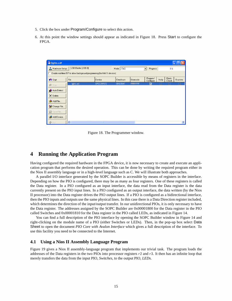
5. Click the box underProgram/Configure to select this action.
6. At this point the window settings should appear as indicated in Figure 18. PressStart to configure theFPGA.
Figure 18. The Programmer window.
4 Running the Application Program
Having configured the required hardware in the FPGA device, it is now necessary to create and execute an appli-cation program that performs the desired operation. This can be done by writing the required program either inthe Nios II assembly language or in a high-level language such as C. We will illustrate both approaches.
A parallel I/O interface generated by the SOPC Builder is accessible by means of registers in the interface.Depending on how the PIO is configured, there may be as many as four registers. One of these registers is calledthe Data register. In a PIO configured as an input interface, the data read from the Data register is the datacurrently present on the PIO input lines. In a PIO configured as an output interface, the data written (by the NiosII processor) into the Data register drives the PIO output lines. If a PIO is configured as a bidirectional interface,then the PIO inputs and outputs use the same physical lines. In this case there is a Data Direction register included,which determines the direction of the input/output transfer. In our unidirectional PIOs, it is only necessary to havethe Data register. The addresses assigned by the SOPC Builder are 0x00001800 for the Data register in the PIOcalled Switches and 0x00001810 for the Data register in the PIO called LEDs, as indicated in Figure 14.
You can find a full description of the PIO interface by openingthe SOPC Builder window in Figure 14 andright-clicking on the module name of a PIO (either Switches or LEDs). Then, in the pop-up box selectDataSheet to open the documentPIO Core with Avalon Interfacewhich gives a full description of the interface. Touse this facility you need to be connected to the Internet.
4.1 Using a Nios II Assembly Language Program
Figure 19 gives a Nios II assembly-language program that implements our trivial task. The program loads theaddresses of the Data registers in the two PIOs into processor registersr2 andr3. It then has an infinite loop thatmerely transfers the data from the input PIO,Switches, to the output PIO,LEDs.
15

.include "nios_macros.s"
.equ Switches, 0x00001800
.equ LEDs, 0x00001810
.global _start_start:
movia r2, Switchesmovia r3, LEDs
loop: ldbio r4, 0(r2)stbio r4, 0(r3)br loop
Figure 19. Assembly language code to control the lights.
The program includes the assembler directive
.include "nios_macros.s"
which informs the Assembler to use the Nios II macros that specify how themovia pseudoinstructions can beassembled.
The directive
.global _start
indicates to the Assembler that the label_start is accessible outside the assembled object file. This label is thedefault label we use to indicate to the Linker program the beginning of the application program.
For a detailed explanation of the Nios II assembly language instructions see the tutorialIntroduction to theAltera Nios II Soft Processor.
Enter this code into a filelights.sand place the file into a working directory. We placed the file into thedirectorysopc_builder_tutorial\app_software. The program has to be assembled and converted into an S-Recordfile, lights.srec, suitable for downloading into the implemented Nios II system.
Altera provides themonitorsoftware, calledAltera Debug Client, for use with the DE2 board. This softwareprovides a simple means for compiling, assembling and downloading of programs into a Nios II system imple-mented on a DE2 board. It also makes it possible for the user toperform debugging tasks. A description of thissoftware is available in theAltera Debug Clienttutorial.
Open the Altera Debug Client, which leads to the window in Figure 20. This software needs to know thecharacteristics of the designed Nios II system, which are given in the ptf filenios_system.ptf. Click theNios II >Configure system... menu item to display the Nios II System Configuration window,shown in Figure 21, andperform the following steps:
1. Select theUSB-Blastercable from theCable drop-down list, which is used with DE2 board.
2. Click Browse... to display a file selection window and choose thenios_system.ptffile. Note that this file isin the design directorysopc_builder_tutorial.
3. Click Load.
4. The Altera Debug Client also needs to know where to load theapplication program. In our case, this is thememory block in the FPGA device. The SOPC Builder assigned the nameonchip_memory_0to this block.As shown in Figure 21, the Debug Client has already selected the correct memory device.
5. Having provided the necessary information, clickOk to confirm the system configuration.
16

Next, the source filelights.sneeds to be specified. Click theNios II > Configure program... menu item todisplay the Nios II Program Configuration window in Figure 22and perform the following steps:
1. Click Add... to display a file selection window and choose thelights.sfile. Note that this file is in thedirectorysopc_builder_tutorial\app_software.
2. Click Ok to confirm the program configuration.
Next, to assemble and download thelight.sprogram, click theActions > Compile & Load menu item. TheAltera Debug Client will invoke an assembler program, followed by a linker program. The commands used toinvoke these programs, and the output they produce, can be viewed in theInfo & Errors window of the DebugClient window. After the program has been downloaded onto the board, the program is displayed in theDisas-sembly window of the Debug Client as illustrated in Figure 23. Observe thatmovia is apseudoinstructionwhichis implemented as two separate instructions.
Click theActions > Continue menu item to execute the program. With the program running, you can nowtest the design by turning the switches,SW7 to SW0 on and off; the LEDs should respond accordingly.
The Debug Client allows a number of useful functions to be performed in a simple manner. They include:
• single stepping through the program
• examining the contents of processor registers
• examining the contents of the memory
• setting breakpoints for debugging purposes
• disassembling the downloaded program
A description of this software and all of its features is available in theAltera Debug Clienttutorial.
17
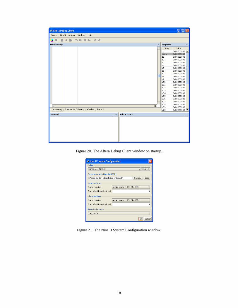
Figure 20. The Altera Debug Client window on startup.
Figure 21. The Nios II System Configuration window.
18
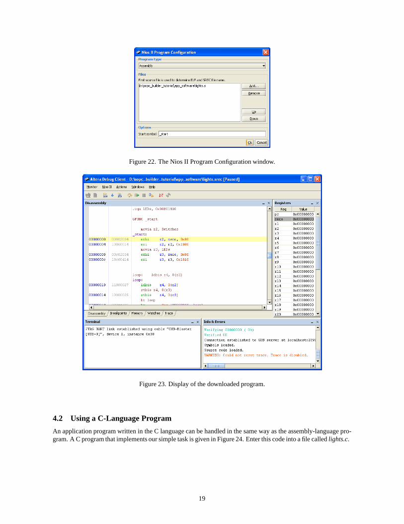
Figure 22. The Nios II Program Configuration window.
Figure 23. Display of the downloaded program.
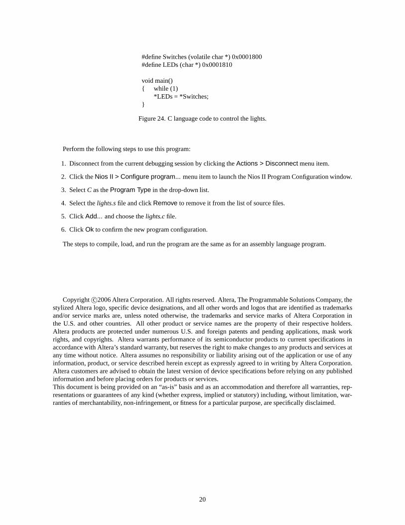
4.2 Using a C-Language Program
An application program written in the C language can be handled in the same way as the assembly-language pro-gram. A C program that implements our simple task is given in Figure 24. Enter this code into a file calledlights.c.
19
#define Switches (volatile char *) 0x0001800#define LEDs (char *) 0x0001810
void main(){ while (1)
*LEDs = *Switches;}
Figure 24. C language code to control the lights.
Perform the following steps to use this program:
1. Disconnect from the current debugging session by clicking theActions > Disconnect menu item.
2. Click theNios II > Configure program... menu item to launch the Nios II Program Configuration window.
3. SelectC as theProgram Type in the drop-down list.
4. Select thelights.sfile and clickRemove to remove it from the list of source files.
5. Click Add... and choose thelights.cfile.
6. Click Ok to confirm the new program configuration.
The steps to compile, load, and run the program are the same asfor an assembly language program.
Copyright c©2006 Altera Corporation. All rights reserved. Altera, The Programmable Solutions Company, thestylized Altera logo, specific device designations, and allother words and logos that are identified as trademarksand/or service marks are, unless noted otherwise, the trademarks and service marks of Altera Corporation inthe U.S. and other countries. All other product or service names are the property of their respective holders.Altera products are protected under numerous U.S. and foreign patents and pending applications, mask workrights, and copyrights. Altera warrants performance of itssemiconductor products to current specifications inaccordance with Altera’s standard warranty, but reserves the right to make changes to any products and services atany time without notice. Altera assumes no responsibility or liability arising out of the application or use of anyinformation, product, or service described herein except as expressly agreed to in writing by Altera Corporation.Altera customers are advised to obtain the latest version ofdevice specifications before relying on any publishedinformation and before placing orders for products or services.This document is being provided on an “as-is” basis and as an accommodation and therefore all warranties, rep-resentations or guarantees of any kind (whether express, implied or statutory) including, without limitation, war-ranties of merchantability, non-infringement, or fitness for a particular purpose, are specifically disclaimed.
20