tuning of microtoroid resonators - arXiv · High bandwidth on-chip capacitive tuning of microtoroid...
11
High bandwidth on-chip capacitive tuning of microtoroid resonators Christopher G. Baker * , Christiaan Bekker, David L. McAuslan, Eoin Sheridan, and Warwick P. Bowen Queensland Quantum Optics Laboratory, University of Queensland, Brisbane, Queensland 4072, Australia * [email protected] Abstract: We report on the design, fabrication and characterization of silica microtoroid based cavity opto-electromechanical systems (COEMS). Electrodes patterned onto the microtoroid resonators allow for rapid capacitive tuning of the optical whispering gallery mode resonances while maintaining their ultrahigh quality factor, enabling applications such as efficient radio to optical frequency conversion, optical routing and switching applications. © 2016 Optical Society of America OCIS codes: (220.4880) Optomechanics; 130.7405 (Wavelength conversion devices); 250.3140 (Integrated optoelectronic circuits) 230.3120 (Integrated optics devices); 230.4000 (Microstructure fabrication) References and links 1. G. Anetsberger, R. Rivi` ere, A. Schliesser, O. Arcizet, and T. J. Kippenberg, “Ultralow-dissipation optomechanical resonators on a chip,” Nature Photonics 2, 627–633 (2008). 2. J. Rosenberg, Q. Lin, and O. Painter, “Static and dynamic wavelength routing via the gradient optical force,” Nat Photon 3, 478–483 (2009). 3. G. I. Harris, D. L. McAuslan, E. Sheridan, Y. Sachkou, C. Baker, and W. P. Bowen, “Laser cooling and control of excitations in superfluid helium,” Nature Physics advance online publication (2016). 4. E. Verhagen, S. Delglise, S. Weis, A. Schliesser, and T. J. Kippenberg, “Quantum-coherent coupling of a me- chanical oscillator to an optical cavity mode,” Nature 482, 63–67 (2012). 5. E. Gil-Santos, C. Baker, D. T. Nguyen, W. Hease, C. Gomez, A. Lemaitre, S. Ducci, G. Leo, and I. Favero, “High-frequency nano-optomechanical disk resonators in liquids,” Nature Nanotechnology 10, 810–816 (2015). 6. K. Lee, T. McRae, G. Harris, J. Knittel, and W. Bowen, “Cooling and Control of a Cavity Optoelectromechanical System,” Phys. Rev. Lett. 104, 123604 (2010). 7. C. Errando-Herranz, F. Niklaus, G. Stemme, and K. B. Gylfason, “Low-power microelectromechanically tunable silicon photonic ring resonator add–drop filter,” Optics letters 40, 3556–3559 (2015). 8. H. Lee, T. Chen, J. Li, K. Y. Yang, S. Jeon, O. Painter, and K. J. Vahala, “Chemically etched ultrahigh-Q wedge- resonator on a silicon chip,” Nat Photon 6, 369–373 (2012). 9. F. Vollmer and S. Arnold, “Whispering-gallery-mode biosensing: label-free detection down to single molecules,” Nature methods 5, 591–596 (2008). 10. S. Forstner, E. Sheridan, J. Knittel, C. L. Humphreys, G. A. Brawley, H. Rubinsztein-Dunlop, and W. P. Bowen, “Ultrasensitive Optomechanical Magnetometry,” Adv. Mater. 26, 6348–6353 (2014). 11. P. DelHaye, A. Schliesser, O. Arcizet, T. Wilken, R. Holzwarth, and T. Kippenberg, “Optical frequency comb generation from a monolithic microresonator,” Nature 450, 1214–1217 (2007). 12. E. Gil-Santos, C. Baker, A. Lemaitre, C. Gomez, S. Ducci, G. Leo, and I. Favero, “High-precision spectral tuning of micro and nanophotonic cavities by resonantly enhanced photoelectrochemical etching,” arXiv:1511.06186 [physics] (2015). ArXiv: 1511.06186. 13. E. J. Klein, D. H. Geuzebroek, H. Kelderman, G. Sengo, N. Baker, and A. Driessen, “Reconfigurable optical add-drop multiplexer using microring resonators,” IEEE Photonics Technology Letters 17, 2358–2360 (2005). 14. M. Zhang, G. S. Wiederhecker, S. Manipatruni, A. Barnard, P. McEuen, and M. Lipson, “Synchronization of Micromechanical Oscillators Using Light,” Physical Review Letters 109, 233906 (2012). arXiv:1605.07281v1 [physics.optics] 24 May 2016
Transcript of tuning of microtoroid resonators - arXiv · High bandwidth on-chip capacitive tuning of microtoroid...
High bandwidth on-chip capacitivetuning of microtoroid resonators
Christopher G. Baker∗, Christiaan Bekker, David L. McAuslan, EoinSheridan, and Warwick P. Bowen
Queensland Quantum Optics Laboratory, University of Queensland, Brisbane, Queensland4072, Australia
Abstract: We report on the design, fabrication and characterization ofsilica microtoroid based cavity opto-electromechanical systems (COEMS).Electrodes patterned onto the microtoroid resonators allow for rapidcapacitive tuning of the optical whispering gallery mode resonances whilemaintaining their ultrahigh quality factor, enabling applications such asefficient radio to optical frequency conversion, optical routing and switchingapplications.
© 2016 Optical Society of America
OCIS codes: (220.4880) Optomechanics; 130.7405 (Wavelength conversion devices);250.3140 (Integrated optoelectronic circuits) 230.3120 (Integrated optics devices); 230.4000(Microstructure fabrication)
References and links1. G. Anetsberger, R. Riviere, A. Schliesser, O. Arcizet, and T. J. Kippenberg, “Ultralow-dissipation optomechanical
resonators on a chip,” Nature Photonics 2, 627–633 (2008).2. J. Rosenberg, Q. Lin, and O. Painter, “Static and dynamic wavelength routing via the gradient optical force,” Nat
Photon 3, 478–483 (2009).3. G. I. Harris, D. L. McAuslan, E. Sheridan, Y. Sachkou, C. Baker, and W. P. Bowen, “Laser cooling and control
of excitations in superfluid helium,” Nature Physics advance online publication (2016).4. E. Verhagen, S. Delglise, S. Weis, A. Schliesser, and T. J. Kippenberg, “Quantum-coherent coupling of a me-
chanical oscillator to an optical cavity mode,” Nature 482, 63–67 (2012).5. E. Gil-Santos, C. Baker, D. T. Nguyen, W. Hease, C. Gomez, A. Lemaitre, S. Ducci, G. Leo, and I. Favero,
“High-frequency nano-optomechanical disk resonators in liquids,” Nature Nanotechnology 10, 810–816 (2015).6. K. Lee, T. McRae, G. Harris, J. Knittel, and W. Bowen, “Cooling and Control of a Cavity Optoelectromechanical
System,” Phys. Rev. Lett. 104, 123604 (2010).7. C. Errando-Herranz, F. Niklaus, G. Stemme, and K. B. Gylfason, “Low-power microelectromechanically tunable
silicon photonic ring resonator add–drop filter,” Optics letters 40, 3556–3559 (2015).8. H. Lee, T. Chen, J. Li, K. Y. Yang, S. Jeon, O. Painter, and K. J. Vahala, “Chemically etched ultrahigh-Q wedge-
resonator on a silicon chip,” Nat Photon 6, 369–373 (2012).9. F. Vollmer and S. Arnold, “Whispering-gallery-mode biosensing: label-free detection down to single molecules,”
Nature methods 5, 591–596 (2008).10. S. Forstner, E. Sheridan, J. Knittel, C. L. Humphreys, G. A. Brawley, H. Rubinsztein-Dunlop, and W. P. Bowen,
“Ultrasensitive Optomechanical Magnetometry,” Adv. Mater. 26, 6348–6353 (2014).11. P. DelHaye, A. Schliesser, O. Arcizet, T. Wilken, R. Holzwarth, and T. Kippenberg, “Optical frequency comb
generation from a monolithic microresonator,” Nature 450, 1214–1217 (2007).12. E. Gil-Santos, C. Baker, A. Lemaitre, C. Gomez, S. Ducci, G. Leo, and I. Favero, “High-precision spectral tuning
of micro and nanophotonic cavities by resonantly enhanced photoelectrochemical etching,” arXiv:1511.06186[physics] (2015). ArXiv: 1511.06186.
13. E. J. Klein, D. H. Geuzebroek, H. Kelderman, G. Sengo, N. Baker, and A. Driessen, “Reconfigurable opticaladd-drop multiplexer using microring resonators,” IEEE Photonics Technology Letters 17, 2358–2360 (2005).
14. M. Zhang, G. S. Wiederhecker, S. Manipatruni, A. Barnard, P. McEuen, and M. Lipson, “Synchronization ofMicromechanical Oscillators Using Light,” Physical Review Letters 109, 233906 (2012).
arX
iv:1
605.
0728
1v1
[ph
ysic
s.op
tics]
24
May
201
6
15. D. Armani, T. Kippenberg, S. Spillane, and K. Vahala, “Ultra-high-q toroid microcavity on a chip,” Nature 421,925–928 (2003).
16. D. Armani, B. Min, A. Martin, and K. J. Vahala, “Electrical thermo-optic tuning of ultrahigh-q microtoroidresonators,” Applied physics letters 85, 5439–5441 (2004).
17. K. D. Heylman and R. H. Goldsmith, “Photothermal mapping and free-space laser tuning of toroidal opticalmicrocavities,” Applied Physics Letters 103, 211116 (2013).
18. W. Bogaerts, P. De Heyn, T. Van Vaerenbergh, K. De Vos, S. Kumar Selvaraja, T. Claes, P. Dumon, P. Bienstman,D. Van Thourhout, and R. Baets, “Silicon microring resonators,” Laser & Photonics Reviews 6, 47–73 (2012).
19. M. Pollinger, D. OShea, F. Warken, and A. Rauschenbeutel, “Ultrahigh-q tunable whispering-gallery-mode mi-croresonator,” Physical review letters 103, 053901 (2009).
20. M. Sumetsky, Y. Dulashko, and R. Windeler, “Super free spectral range tunable optical microbubble resonator,”Optics letters 35, 1866–1868 (2010).
21. L. Yang, D. Armani, and K. Vahala, “Fiber-coupled erbium microlasers on a chip,” Applied physics letters 83,825–826 (2003).
22. T. Kippenberg, S. Spillane, D. Armani, and K. Vahala, “Ultralow-threshold microcavity raman laser on a micro-electronic chip,” Optics letters 29, 1224–1226 (2004).
23. H. Jung, K. Y. Fong, C. Xiong, and H. X. Tang, “Electrical tuning and switching of an optical frequency combgenerated in aluminum nitride microring resonators,” Optics Letters 39, 84 (2014).
24. S. A. Miller, Y. Okawachi, S. Ramelow, K. Luke, A. Dutt, A. Farsi, A. L. Gaeta, and M. Lipson, “Tunablefrequency combs based on dual microring resonators,” Opt. Express 23, 21527–21540 (2015).
25. C. Baker, W. Hease, D.-T. Nguyen, A. Andronico, S. Ducci, G. Leo, and I. Favero, “Photoelastic coupling ingallium arsenide optomechanical disk resonators,” Opt. Express 22, 14072–14086 (2014).
26. W. P. Bowen and G. J. Milburn, Quantum optomechanics (CRC Press, 2015).27. A. Pitanti, J. M. Fink, A. H. Safavi-Naeini, J. T. Hill, C. U. Lei, A. Tredicucci, and O. Painter, “Strong opto-
electro-mechanical coupling in a silicon photonic crystal cavity,” Opt. Express 23, 3196–3208 (2015).28. S. Abdulla, L. Kauppinen, M. Dijkstra, M. de Boer, E. Berenschot, H. Jansen, R. de Ridder, and G. Krijnen,
“Tuning a racetrack ring resonator by an integrated dielectric MEMS cantilever,” Optics Express 19, 15864(2011).
29. M. Winger, T. D. Blasius, T. P. Mayer Alegre, A. H. Safavi-Naeini, S. Meenehan, J. Cohen, S. Stobbe, andO. Painter, “A chip-scale integrated cavity-electro-optomechanics platform,” Opt. Express 19, 24905–24921(2011).
30. T. Bagci, A. Simonsen, S. Schmid, L. G. Villanueva, E. Zeuthen, J. Appel, J. M. Taylor, A. Srensen, K. Usami,A. Schliesser, and E. S. Polzik, “Optical detection of radio waves through a nanomechanical transducer,” Nature507, 81–85 (2014).
31. D. T. Nguyen, C. Baker, W. Hease, S. Sejil, P. Senellart, A. Lemaitre, S. Ducci, G. Leo, and I. Favero, “Ultrahighq-frequency product for optomechanical disk resonators with a mechanical shield,” Applied Physics Letters 103,241112 (2013).
32. X. Jiang, Q. Lin, J. Rosenberg, K. Vahala, and O. Painter, “High-Q double-disk microcavities for cavity optome-chanics,” Optics Express 17, 20911–20919 (2009).
33. R. W. Andrews, R. W. Peterson, T. P. Purdy, K. Cicak, R. W. Simmonds, C. A. Regal, and K. W. Lehnert, “Bidi-rectional and efficient conversion between microwave and optical light,” Nature Physics 10, 321–326 (2014).
34. P. Slade and E. Taylor, “Electrical breakdown in atmospheric air between closely spaced (0.2 m-40 m) electricalcontacts,” IEEE Transactions on Components and Packaging Technologies 25, 390–396 (2002).
1. Introduction
High optical quality factor (Q) cavities, and in particular whispering gallery mode (WGM) res-onators are broadly used optical components. Due to the combination of high Q and low modevolume, they are a platform of choice for a wide range of applications including optomechanics[1, 2, 3, 4, 5], optoelectromechanics [6], optical add-drop filters [7], on-chip lasers [8], bio- andmagnetic sensing [9, 10] and frequency comb generation [11]. The ability to spectrally tunethe WGM resonances of these resonators, preferably in a reversible fashion, is of great interestfor many of these applications. This tunability can for instance be used to overcome microfab-rication induced size variability [12] or temperature associated frequency drifts, lessening theneed for bulky and expensive tunable laser sources. It also permits optical switching, reconfig-urable optical routing [13] and is required for any kind of on-chip network of interacting highQ resonators [14].
Silica is a particularly advantageous material for on- and off-chip photonics thanks to its ex-
tremely low optical absorption, low susceptibility to two-photon absorption and associated freecarrier absorption, and the absence of lossy surface states requiring passivation. In particularsilica microtoroids [15] and silica wedge resonators [8] set the benchmark for the highest op-tical Q resonators achievable on a chip, with Q values reaching almost 1 billion [8]. However,silica resonators are difficult to tune due to the absence of free carrier injection schemes andvanishing linear electro-optic coefficient. Two main approaches have been employed thus far:heat-based and strain-based methods. Heat-based tuning [16, 17] relies on changing the size andrefractive index of the material with temperature, and, while allowing for large frequency shifts,suffers from several drawbacks. First, owing to silica’s low thermo-optic and thermal expan-sion coefficients, high temperatures are required for large wavelength shifts, requiring typicallytens of milliwatts of power expenditure [18] and precluding cryogenic or biological applica-tions. Furthermore this tuning method is inherently slow, with modulation rates constrained tothe kHz range for microtoroids [16, 17]. Strain coupling, whereby the resonator is subjectedto stress and deformed, thus changing its effective size and optical resonance frequencies hasbeen demonstrated on silica bottle resonators [19, 20] but not for integrated on-chip resonators.
Here we propose and experimentally demonstrate an efficient strain coupling approach totune the high Q resonances of on-chip WGM resonators, based upon capacitive actuation. Goldelectrodes are patterned upon the top surface of the device to be tuned. When a bias voltageis applied, the attractive capacitive force between the electrodes strains the device and shiftsthe position of its optical resonances. Our approach presents several advantages. First it al-lows for very fast electrical tuning of the resonances reaching up to the tens of MHz range,several orders of magnitude faster than previously demonstrated schemes, while maintainingthe ultra-high Q nature of the resonances. Moreover, capacitive tuning requires minimal powerexpenditure as there is no current flow between the electrodes in the steady state. This enablesdense arrays of tuneable microresonators to be combined on a single chip, with low power con-sumption compatible with packaged devices and without the risk of thermal crosstalk betweenneighbouring devices. Finally, we present numerical simulations of a new design based uponinterdigitated electrodes which significantly improves upon the performance of the current de-vices. Our approach could have applications for silica microtoroid and microdisk based erbiumlasers [21], Raman and Brillouin lasers [22, 8] as well as tuneable and switchable frequencycombs [23, 24].
2. Device design and fabrication
2.1. Design
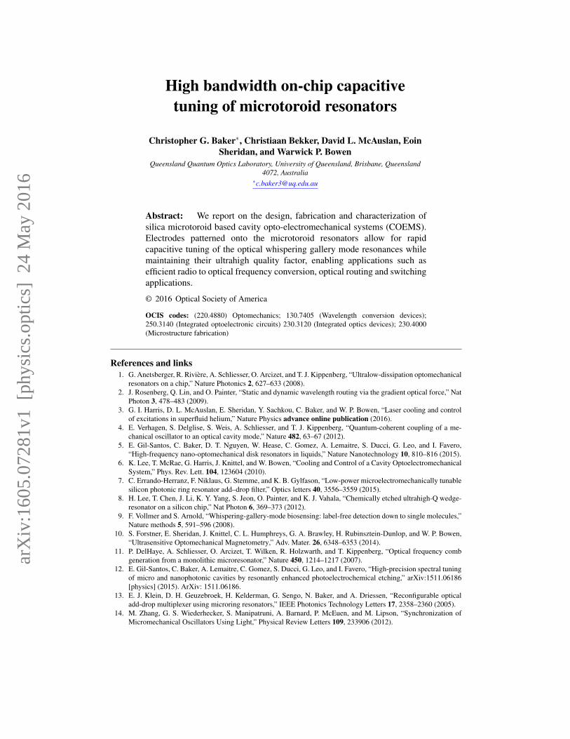
Figure 1(a) shows a schematic top view of the designed device. It consists of a reflown silicamicrotoroid resonator [15], in which a circular slot of width g has been etched out, in orderto allow for greater mechanical compliance. Gold electrodes are patterned on either side ofthis slot to enable capacitive actuation. Upon the application of a bias voltage between theelectrodes through the contact pads P1 and P2, the attractive capacitive force strains the mi-crotoroid resulting in an effective reduction in the microtoroid cavity length and an associatedfrequency shift of the microtoroid whispering gallery resonances. The outer portion of the sil-ica microtoroid is mechanically supported by a single anchor which also serves to connect theouter electrode to the contact pad P1. The position of this anchor is marked by an asterisk inFigure 1(a). Even with a single narrow anchor, the sag of the outer portion of the microtoroidis minimal as confirmed by finite element method (FEM) simulations.
d
R Rp
g
50 um
(a) (b)
*
P1
P2
Fig. 1. Microtoroid based COEMS. (a) Schematic top view of the microtoroid COEMSdisplaying the relevant dimensions: microtoroid major radius R, microtoroid minor diam-eter d, electrode gap g and undercut silicon pedestal radius Rp. The gold electrodes havea nominal width of 5 microns. (b) Optical microscope side-view of a fabricated device.This image was obtained by combining 10 individual images taken at different focus toovercome the shallow depth of field (focus stacking).
2.2. Modeling
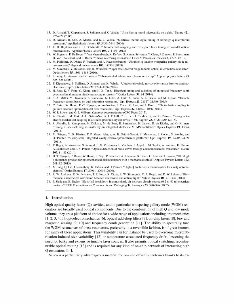
The application of a bias voltage V between the electrodes leads to an attractive capacitive forceFcap:
Fcap =12
dC (x)dx×V 2 (1)
Here x is a displacement and C (x) is the position dependent capacitance formed by the twocapacitor plates, see Fig. 2(a). The value of C (x) for our device is extracted from FEM simula-tions and plotted as a function of the gap between the electrodes in the top panel of Fig. 2(b).The associated force Fcap/V 2 given by Eq. (1) is plotted in the lower panel. The capacitive forceleads to a deformation of the outer ring ∆x and a shift in the WGM resonance frequencies ∆ω0given by:
∆ω0 = gom∆x = gomFcap
k' 1
2kω0
RdC (x)
dxV 2 ≡ αV 2 (2)
where gom ' ω0R is the optomechanical coupling term [25, 26], R the major radius of the mi-
crotoroid, and k = meff Ω2M the effective stiffness of the slotted microtoroid which links the
effective change in radius of the cavity to the applied force. α is the optical tunability of thestructure [27]. With our nominal fabrication parameters (R' 60 microns after reflow, electrodewidth of 5 microns, gap g of 2 to 3 microns), our modeling predicts a tunability α/2π in therange of 3 to 4 kHz/V2.
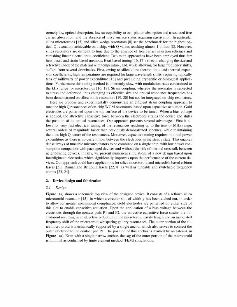
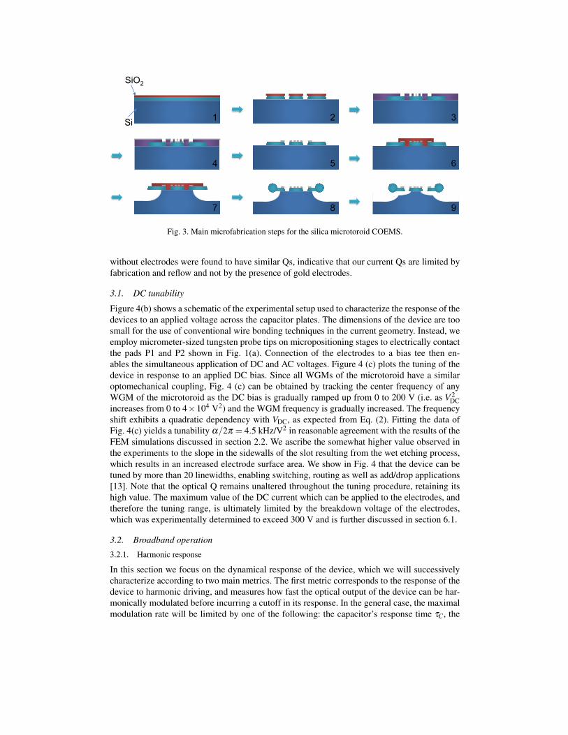
2.3. Fabrication
Figure 3 outlines the main microfabrication steps. Starting from a silicon wafer with a 2 micronthick SiO2 thermal oxide, slotted disks are patterned with standard photolithography using pos-itive resist (AZ 1518 - red layer), followed by a wet buffered oxide etchant (BOE) etch (steps 1and 2). The position of the electrodes is defined in step 3, using a mask aligner and negative liftoff resist (AZ nLOF 2020 - purple). Next a 10 nm thick tungsten adhesion layer and 100 nm
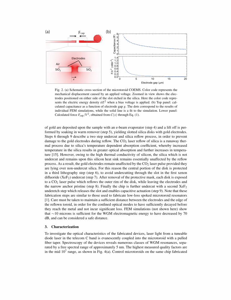
(a) (b)Fcap
Air
SiO2
Electrodes
SiO2
x
0123456
Cap
acita
nce(fF
)
0 5 10 15 200.00.20.40.60.81.01.21.4
Electrode gap (μm)
F /V
2(n
N/V
2 )
Fig. 2. (a) Schematic cross section of the microtoroid COEMS. Color code represents themechanical displacement caused by an applied voltage. Zoomed in view shows the elec-trodes positioned on either side of the slot etched in the silica. Here the color code repre-sents the electric energy density εE2 when a bias voltage is applied. (b) Top panel: cal-culated capacitance as a function of electrode gap g. The dots correspond to the results ofindividual FEM simulations, while the solid line is a fit to the simulation. Lower panel:Calculated force Fcap/V 2, obtained from C(x) through Eq. (1).
of gold are deposited upon the sample with an e-beam evaporator (step 4) and a lift off is per-formed by soaking in warm remover (step 5), yielding slotted silica disks with gold electrodes.Steps 6 through 9 describe a two step undercut and silica reflow process, in order to preventdamage to the gold electrodes during reflow. The CO2 laser reflow of silica is a runaway ther-mal process due to silica’s temperature dependent absorption coefficient, whereby increasedtemperature in the silica results in greater optical absorption and further increases in tempera-ture [15]. However, owing to the high thermal conductivity of silicon, the silica which is notundercut and remains upon this silicon heat sink remains essentially unaffected by the reflowprocess. As a result, the gold electrodes remain unaffected by the CO2 laser pulse provided theyare lying over non-undercut silica. For this reason the central portion of the disk is protectedin a third lithography step (step 6), to avoid undercutting through the slot in the first xenondifluoride (XeF2) undercut (step 7). After removal of the protective mask, each disk is exposedto a CO2 laser pulse which reflows the outer rim of the disk, while leaving the electrodes andthe narrow anchor pristine (step 8). Finally the chip is further undercut with a second XeF2underetch step which releases the slot and enables capacitive actuation (step 9). Note that thesefabrication steps are similar to those used to fabricate low-loss spoked microtoroid resonators[1]. Care must be taken to maintain a sufficient distance between the electrodes and the edge ofthe reflown toroid, in order for the confined optical modes to have sufficiently decayed beforethey reach the metal and not incur significant loss. FEM simulations (not shown here) showthat ∼10 microns is sufficient for the WGM electromagnetic energy to have decreased by 70dB, and can be considered a safe distance.
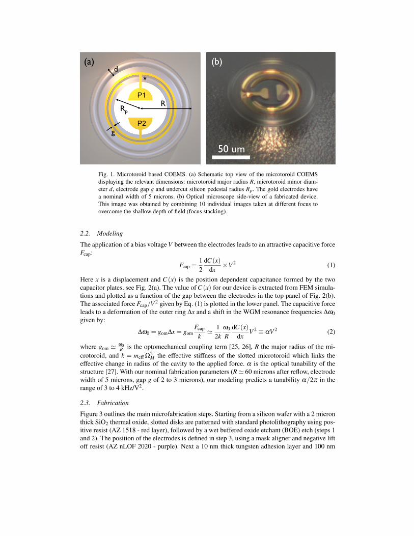
3. Characterization
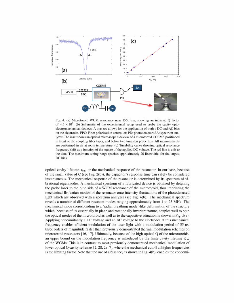
To investigate the optical characteristics of the fabricated devices, laser light from a tuneablediode laser in the telecom C band is evanescently coupled into the microtoroid with a pulledfiber taper. Spectroscopy of the devices reveals numerous classes of WGM resonances, sepa-rated by a free spectral range of approximately 5 nm. The highest measured quality factors arein the mid 107 range, as shown in Fig. 4(a). Control microtoroids on the same chip fabricated
Si
SiO2
1 2 3
4 5 6
7 8 9
Fig. 3. Main microfabrication steps for the silica microtoroid COEMS.
without electrodes were found to have similar Qs, indicative that our current Qs are limited byfabrication and reflow and not by the presence of gold electrodes.
3.1. DC tunability
Figure 4(b) shows a schematic of the experimental setup used to characterize the response of thedevices to an applied voltage across the capacitor plates. The dimensions of the device are toosmall for the use of conventional wire bonding techniques in the current geometry. Instead, weemploy micrometer-sized tungsten probe tips on micropositioning stages to electrically contactthe pads P1 and P2 shown in Fig. 1(a). Connection of the electrodes to a bias tee then en-ables the simultaneous application of DC and AC voltages. Figure 4 (c) plots the tuning of thedevice in response to an applied DC bias. Since all WGMs of the microtoroid have a similaroptomechanical coupling, Fig. 4 (c) can be obtained by tracking the center frequency of anyWGM of the microtoroid as the DC bias is gradually ramped up from 0 to 200 V (i.e. as V 2
DCincreases from 0 to 4×10⁴ V2) and the WGM frequency is gradually increased. The frequencyshift exhibits a quadratic dependency with VDC, as expected from Eq. (2). Fitting the data ofFig. 4(c) yields a tunability α/2π = 4.5 kHz/V2 in reasonable agreement with the results of theFEM simulations discussed in section 2.2. We ascribe the somewhat higher value observed inthe experiments to the slope in the sidewalls of the slot resulting from the wet etching process,which results in an increased electrode surface area. We show in Fig. 4 that the device can betuned by more than 20 linewidths, enabling switching, routing as well as add/drop applications[13]. Note that the optical Q remains unaltered throughout the tuning procedure, retaining itshigh value. The maximum value of the DC current which can be applied to the electrodes, andtherefore the tuning range, is ultimately limited by the breakdown voltage of the electrodes,which was experimentally determined to exceed 300 V and is further discussed in section 6.1.
3.2. Broadband operation
3.2.1. Harmonic response
In this section we focus on the dynamical response of the device, which we will successivelycharacterize according to two main metrics. The first metric corresponds to the response of thedevice to harmonic driving, and measures how fast the optical output of the device can be har-monically modulated before incurring a cutoff in its response. In the general case, the maximalmodulation rate will be limited by one of the following: the capacitor’s response time τC, the
0 1x10⁴ 2x10⁴ 3x10⁴ 4x10⁴
0
20
40
60
80
100
120
140
160
180
V2DC (V
2)
Freq
uenc
y sh
ift (M
Hz)
0.0
0.2
0.4
0.6
0.8
1.0
Nor
mal
ized
Tra
nsm
issi
on
Detuning (MHz)
9 MHz
(a)
(b)
(c)
COEMS
LASERFPC
PD
SA
~DC
Fig. 4. (a) Microtoroid WGM resonance near 1550 nm, showing an intrinsic Q factorof 4.5× 10⁷. (b) Schematic of the experimental setup used to probe the cavity opto-electromechanical devices. A bias tee allows for the application of both a DC and AC biason the electrodes. FPC: Fiber polarization controller; PD: photodetector; SA: spectrum ana-lyzer. The inset shows an optical microscope sideview of a microtoroid COEMS positionedin front of the coupling fiber taper, and below two tungsten probe tips. All measurementsare performed in air at room temperature. (c) Tunability curve showing optical resonancefrequency shift as a function of the square of the applied DC voltage. The red line is a fit tothe data. The maximum tuning range reaches approximately 20 linewidths for the largestDC bias.
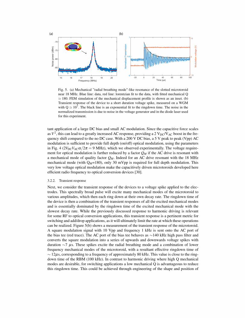
optical cavity lifetime τcav or the mechanical response of the resonator. In our case, becauseof the small value of C (see Fig. 2(b)), the capacitor’s response time can safely be consideredinstantaneous. The mechanical response of the resonator is determined by its spectrum of vi-brational eigenmodes. A mechanical spectrum of a fabricated device is obtained by detuningthe probe laser to the blue side of a WGM resonance of the microtoroid, thus imprinting themechanical Brownian motion of the resonator onto intensity fluctuations of the photodetectedlight which are observed with a spectrum analyzer (see Fig. 4(b)). The mechanical spectrumreveals a number of different resonant modes ranging approximately from 1 to 25 MHz. Themechanical mode corresponding to a ‘radial breathing mode’-like deformation of the structurewhich, because of its essentially in plane and rotationally invariant nature, couples well to boththe optical modes of the microtoroid as well as to the capacitive actuation is shown in Fig. 5(a).Applying concomitantly a DC voltage and an AC voltage to the electrodes at this mechanicalfrequency enables efficient modulation of the laser light with a modulation period of 55 ns,three orders of magnitude faster than previously demonstrated thermal modulation schemes onmicrotoroid resonators [16, 17]. Ultimately, because of the high optical Q of the microtoroids,an upper bound on the modulation frequency is introduced by the finite cavity lifetime τcavof the WGMs. This is in contrast to most previously demonstrated mechanical modulation oflower optical Q cavity schemes [2, 28, 29, 7], where the mechanical cutoff at higher frequenciesis the limiting factor. Note that the use of a bias tee, as shown in Fig. 4(b), enables the concomi-
Time (μs)-20 0 20 40 60 80 100
Nor
mal
ized
Tra
nsm
issi
on
0
0.5
1
Mod
ulat
ion
volta
ge (V
)
-10
0
10
Frequency (MHz)15 16 17 18 19 20
Noi
se p
ower
(dBm
)
-85
-80
-75
-70
(a) (b)
Fig. 5. (a) Mechanical ”radial breathing mode”-like resonance of the slotted microtoroidnear 18 MHz. Blue line: data, red line: lorentzian fit to the data, with fitted mechanical Q' 180. FEM simulation of the mechanical displacement profile is shown as an inset. (b)Transient response of the device to a short duration voltage spike, measured on a WGMwith Q ' 107. The black line is an exponential fit to the ringdown time. The noise in thenormalized transmission is due to noise in the voltage generator and in the diode laser usedfor this experiment.
tant application of a large DC bias and small AC modulation. Since the capacitive force scalesas V 2, this can lead to a greatly increased AC response, providing a 2 VDC/VAC boost in the fre-quency shift compared to the no DC case. With a 200 V DC bias, a 5 V peak to peak (Vpp) ACmodulation is sufficient to provide full depth (on/off) optical modulation, using the parametersin Fig. 4 (2VDCVACα/2π = 9 MHz), which we observed experimentally. The voltage require-ment for optical modulation is further reduced by a factor QM if the AC drive is resonant witha mechanical mode of quality factor QM . Indeed for an AC drive resonant with the 18 MHzmechanical mode (with QM=180), only 30 mVpp is required for full depth modulation. Thisvery low voltage optical modulation make the capacitively driven microtoroids developed hereefficient radio frequency to optical conversion devices [30].
3.2.2. Transient response
Next, we consider the transient response of the devices to a voltage spike applied to the elec-trodes. This spectrally broad pulse will excite many mechanical modes of the microtoroid tovarious amplitudes, which then each ring down at their own decay rate. The ringdown time ofthe device is then a combination of the transient responses of all the excited mechanical modesand is essentially dominated by the ringdown time of the excited mechanical mode with theslowest decay rate. While the previously discussed response to harmonic driving is relevantfor some RF to optical conversion applications, this transient response is a pertinent metric forswitching and add/drop applications, as it will ultimately limit the rate at which these operationscan be realized. Figure 5(b) shows a measurement of the transient response of the microtoroid.A square modulation signal with 10 Vpp and frequency 1 kHz is sent onto the AC port ofthe bias tee (red trace). The AC port of the bias tee behaves as ∼140 kHz high pass filter andconverts the square modulation into a series of upwards and downwards voltage spikes withduration ∼7 µs. These spikes excite the radial breathing mode and a combination of lowerfrequency mechanical modes of the microtoroid, with a resultant effective ringdown time of∼ 12µs, corresponding to a frequency of approximately 80 kHz. This value is close to the ring-down time of the RBM (100 kHz). In contrast to harmonic driving where high Q mechanicalmodes are desirable, for switching applications a low mechanical Q is advantageous to reducethis ringdown time. This could be achieved through engineering of the shape and position of
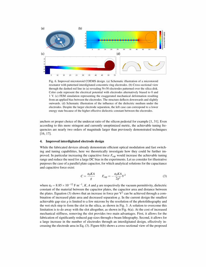
Fig. 6. Improved microtoroid COEMS design. (a) Schematic illustration of a microtoroidresonator with patterned interdigitated concentric ring electrodes. (b) Cross-sectional viewthrough the dashed red line in (a) revealing N=30 electrodes patterned over the silica disk.Color code represent the electrical potential with electrodes alternatively biased to 0 and1 V. (c) FEM simulation representing the exaggerated mechanical deformation resultingfrom an applied bias between the electrodes. The structure deflects downwards and slightlyoutwards. (d) Schematic illustration of the influence of the dielectric medium under theelectrodes. Despite the larger electrode separation, the left case can correspond to a lowerenergy state because of the higher effective dielectric constant between the electrodes.
anchors or proper choice of the undercut ratio of the silicon pedestal for example [1, 31]. Evenaccording to this more stringent and currently unoptimized metric, the achievable tuning fre-quencies are nearly two orders of magnitude larger than previously demonstrated techniques[16, 17].
4. Improved interdigitated electrode design
While the fabricated devices already demonstrate efficient optical modulation and fast switch-ing and tuning capabilities, here we theoretically investigate how they could be further im-proved. In particular increasing the capacitive force Fcap would increase the achievable tuningrange and reduce the need for a large DC bias in the experiments. Let us consider for illustrativepurposes the case of a parallel plate capacitor, for which analytical solutions for the capacitanceand capacitive force exist:
C =ε0KA
gFcap =−
ε0KA2g2 V 2 (3)
where ε0 = 8.85×10⁻¹² F m−1, K, A and g are respectively the vacuum permittivity, dielectricconstant of the material between the capacitor plates, the capacitor area and distance betweenthe plates. Equation (3) shows that an increase in force per V2 can be achieved through a com-bination of increased plate area and decreased separation g. In the current design the smallestachievable gap size g is limited to a few microns by the resolution of the photolithography andthe wet etch step to form the slot in the silica, as shown in Fig. 3. A solution to overcome thislimitation is to do away with the slot altogether, as shown in Fig. 6(a). At the cost of increasedmechanical stiffness, removing the slot provides two main advantages. First, it allows for thefabrication of significantly reduced gap sizes through e-beam lithography. Second, it allows fora large increase in the number of electrodes through an interdigitated design, effectively in-creasing the electrode area in Eq. (3). Figure 6(b) shows a cross-sectional view of the proposed
approach, with 30 electrodes of width 0.9 micron separated by 150 nm patterned on the topsurface. The capacitance calculated for this structure is 250 fF, more than 50 times larger thanin our current design. In order to take into account both the effect of the material between theelectrodes as well as the fact that the applied force is now distributed throughout the micro-toroid surface, we perform full electromechanical FEM simulations to obtain the deformationof the structure in response to an applied bias voltage. The parameters used in this simulationare summarized in Table 1. The results of this simulation, for a 1 V bias applied between theelectrodes, are shown in Fig. 6(c). Here the effect of an applied bias is to deform the structuredownwards and slightly outwards, effectively increasing the microtoroid’s radial dimensions,which is exactly the opposite effect we measured with the slotted microtoroid. This somewhatcounter-intuitive behavior can be understood by considering the stored energy inside a capacitorEcap =
12
Q2
C . For a fixed charge Q, the system will seek to minimize its potential energy throughan increase in C. As shown in Eq. (3), this can be achieved by reducing the gap g between theelectrodes -as observed previously, but can also be achieved through an increase in the effec-tive dielectric constant K of the material between the electrodes. Here the microtoroid bendsdownwards (and not upwards as would be expected from a tensile stress being applied to its topsurface), so as to maximize the amount of dielectric enclosed between the electrodes. This isshown schematically in Fig. 6 (d): provided the dielectric contribution is large enough, the low-est energy solution can actually correspond to an increase in the total separation between theelectrodes (left image). To verify this is the correct interpretation, we numerically verify thatthe downward deflection indeed corresponds to a lower energy state. Furthermore, when addinga high K dielectric coating over the electrodes, the system recovers an upward deflection. Withthe experimentally achievable parameters of Table 1, this optimized geometry provides a tun-ability of α =−0.77 MHz/V2, a more than two orders of magnitude improvement over currentperformance, with a bias on the order of 2 V sufficient to displace a high Q WGM resonance byone linewidth. Note that here most of the generated deformation is out-of-plane, and therefore
Parameter Unit ValueMicrotoroid major radius R µm 50Microtoroid minor diameter d µm 8Pedestal radius Rp µm 4Silica layer thickness µm 2Number of interdigitated electrodes N - 30Electrode width µm 0.9Electrode gap g nm 150Electrode thickness nm 200tunability α MHz/V2 -0.77
Table 1. Parameters used in the FEM simulation of the interdigitated microtoroid COEMSdesign.
not useful as it does not dispersively couple to the microtoroid WGMs. This large out-of planedeflection could however be advantageously leveraged with different resonator geometries [32].
5. Conclusion
We have developed an approach to reversibly tune the optical resonances of high Q on-chipsilica microtoroid resonators based on capacitive actuation, enabled by electrodes patterned onthe top surface of the microresonator. This method provides up to tens of MHz modulationrates, several orders of magnitude faster than previously demonstrated heat based techniques.
We additionally presented an improved design based on interdigitated electrodes that furtherimproves on current performance. These results add a new level of functionality to a matureplatform with a broad range of applications ranging from optomechanics, on chip lasers and bio-sensing to nonlinear optics. Our approach leaves the reflown silica surface intact, and thereforemaintains the high optical Q and the possibility to functionalize the silica surface. It may alsofind use in the active field of RF to optical conversion [30, 29, 27, 33].
Acknowledgments
This work was performed in part at the Queensland node of the Australian National FabricationFacility, a company established under the National Collaborative Research Infrastructure Strat-egy to provide nano and micro-fabrication facilities for Australia’s researchers. This researchwas funded through the Australian Research Council Linkage grant LP140100595. W.P.B. ac-knowledges the Australian Research Council Future Fellowship FT140100650.
6. Appendix
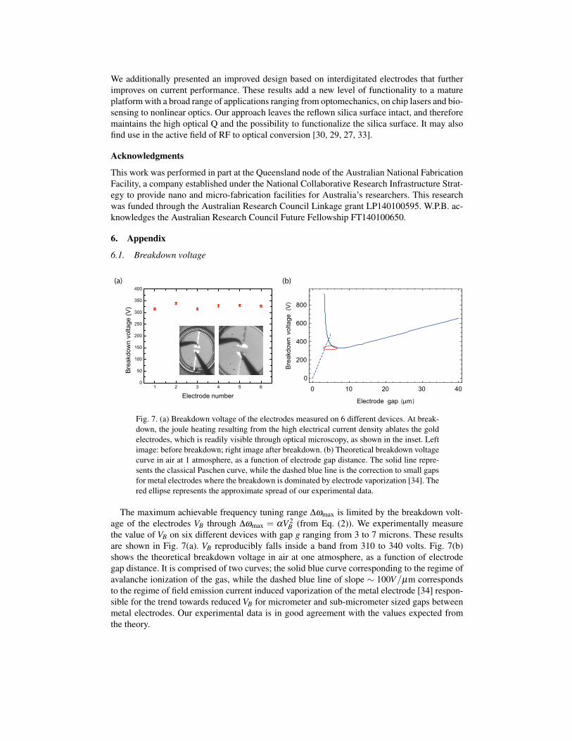
6.1. Breakdown voltage
1 2 3 4 5 60
50
100
150
200
250
300
350
400
Brea
kdow
n vo
ltage
(V)
Electrode number
(a) (b)
0 10 20 30 400
200
400
600
800
Electrode gap (μm )
Brea
kdow
nvo
ltage
(V)
Fig. 7. (a) Breakdown voltage of the electrodes measured on 6 different devices. At break-down, the joule heating resulting from the high electrical current density ablates the goldelectrodes, which is readily visible through optical microscopy, as shown in the inset. Leftimage: before breakdown; right image after breakdown. (b) Theoretical breakdown voltagecurve in air at 1 atmosphere, as a function of electrode gap distance. The solid line repre-sents the classical Paschen curve, while the dashed blue line is the correction to small gapsfor metal electrodes where the breakdown is dominated by electrode vaporization [34]. Thered ellipse represents the approximate spread of our experimental data.
The maximum achievable frequency tuning range ∆ωmax is limited by the breakdown volt-age of the electrodes VB through ∆ωmax = αV 2
B (from Eq. (2)). We experimentally measurethe value of VB on six different devices with gap g ranging from 3 to 7 microns. These resultsare shown in Fig. 7(a). VB reproducibly falls inside a band from 310 to 340 volts. Fig. 7(b)shows the theoretical breakdown voltage in air at one atmosphere, as a function of electrodegap distance. It is comprised of two curves; the solid blue curve corresponding to the regime ofavalanche ionization of the gas, while the dashed blue line of slope ∼ 100V/µm correspondsto the regime of field emission current induced vaporization of the metal electrode [34] respon-sible for the trend towards reduced VB for micrometer and sub-micrometer sized gaps betweenmetal electrodes. Our experimental data is in good agreement with the values expected fromthe theory.