Classes of Polygons Planar polygons –Simple Convex Star-shaped –Non-simple Non-planar polygons.
Tunable Resonance of Star Shaped Nanostructures
R. Diaz de Leon-Zapata1,*2, B. Mora-Ventura 2, M. Jose-Yacaman 3, and F. J. González 2 1Instituto Tecnológico de San Luis Potosí, Av. Tecnológico s/n Soledad de Graciano Sánchez, San Luis Potosí, C.P. 78376, México. 2Universidad Autónoma de San Luis Potosí, Álvaro Obregón 64, San Luis Potosí, San Luis Potosí, C.P. 78000, México. 3University of Texas at San Antonio, 1 UTSA Circle, San Antonio, TX 78249. *[email protected] Abstract: Auto assembled Ag-ZnO [1] star shaped nanostructures depicted in figure 1, presents their natural electromagnetic resonance at 60 THz [2]. In this work we present that is possible changing this value by covering it with a variable in thickness layer of gold. The analysis is performed by numerical simulations using COMSOL Multiphysics®.
Keywords: COMSOL Multiphysics®,
Nanoantennas, FEM simulation.
1. Introduction Recent advances in nano fabrication, electron microscopy imaging and near field microscopy allowed metallic structures to be defined and characterized with sizes comparable or smaller to that of visible light, wavelengths of several hundred nanometers, opened up the possibility of apply nanotechnology and nanoscience in areas with pressing needs, e.g., in sensing, imaging, energy harvesting, and disease cure and prevention, have brought revolutionary improvements.
Metallic nanostructures can convert freely propagating electromagnetic radiation into localized energy, also can control and manipulate optical fields at the nanometer scale. Modifying the geometry and material of nanostructures is possible perform a strong coupling with the magnetic and/or electric component of an incident electromagnetic wave, in which the resonant frequency is dependent on the nanostructure size and shape.
In this work we present the electromagnetic analysis of star shaped nanostructures.
Auto assembled Ag-ZnO [1] star shaped nanostructures depicted in figure 1, presents their natural electromagnetic resonance at 60 THz [2]. Since star shaped geometry showed some interesting interactions with electromagnetic field in the optical regime, it is proposed in this work to adapt the geometry to perform some numerical studies assuming a possible subsequent fabrication by the method of nanolithography, a more convenient method to perform superficial nanoantennas which is the main (but not limited to it) application purpose as will be discussed later in this work. By covering the original auto assembled Ag-ZnO structure (fig. 1) with gold (Au), it is possible to change and adjust their electromagnetic field interaction allowing the purpose of having the directional-enhancer electric field nanostructure.
Figure 1. Star shaped nanostructure.
Excerpt from the Proceedings of the 2016 COMSOL Conference in Boston

1.1 Design parameters of nanostructure for numerical simulations
Figure 2. Design parameter.
Length of arms 0.72 µm Angle 72°
Thickness 0.02 µm Width of arms 0.07 µm
Table 1. Parameter of the star shaped
nanostructures. 2. Computational Methods Using the COMSOL’s RF module [3] to solve equation 1, and applying a planar electromagnetic wave, we can find the interaction of electromagnetic field over the structure for different thickness layer of gold.
∇× ∇×𝐸 − 𝑘!!𝜀!𝐸 = 0 (1)
Equation 1 is obtained by Faraday, Ampere equations and constitutive relations.
∇×𝐻 = 𝐽 + !"!"
(2)
∇×𝐸 = − !"!"
(3)
Using constitutive relations we get:
∇×𝐻 = 𝜎𝐸 + !"#!"
(4)
∇×𝐸 = −𝜇 !"!"
(5)
To perform the simulation, it was constructed a geometry using three different domains, one of them for the star shaped nanostructure, other for covering the nanostructure with air and used as a port to generate the electromagnetic field and applying the scattering boundary condition, and the last one used as a silicon or another material substrate, scattering boundary condition and where the nanostructure is supported or placed.
In order to have a better result we used tetrahedral mesh. Figure 3 shows the mesh of the structure.
Figure 3. Mesh of the geometries
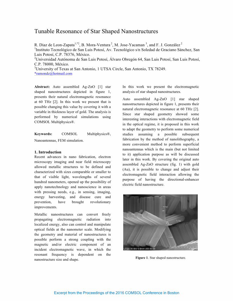
For each different thickness, must be necessary find their respective frequency of resonance where COMSOL’s capabilities are so helpful allowing to perform complex, large and repetitive amount of calculations and presenting the results in a both, qualitative (3D images representing the behavior of electromagnetic field) and quantitative (data, tables and line graphs without any other postprocessing tools or software). For a particular case of a 50 nm of thickness, figure 4 depicts the shape and intensities in their resonance frequency and figure 5 depicts the electromagnetic field intensity response as a function of frequency. As geometry is varying, some other unique properties of COMSOL were used: “Geometry Import” and “LiveLink for Autocad”.
Excerpt from the Proceedings of the 2016 COMSOL Conference in Boston
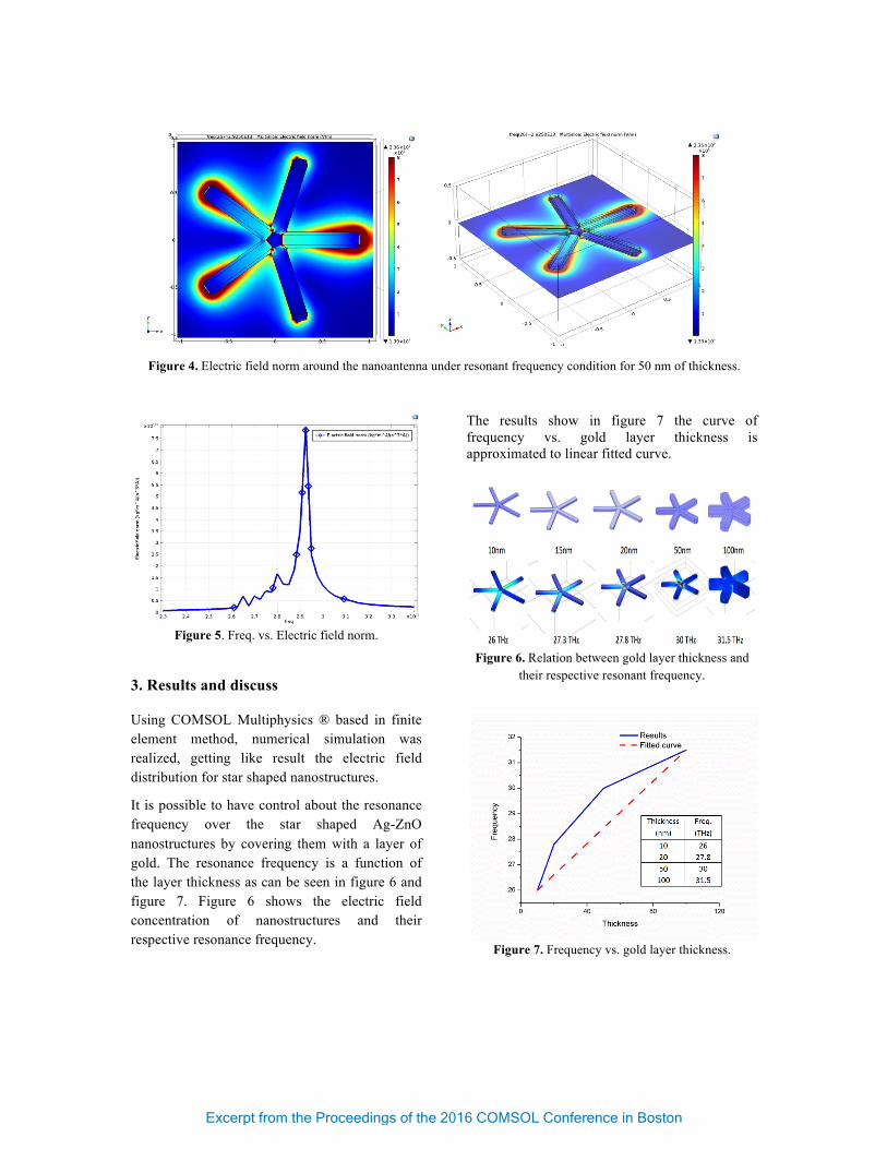
Figure 4.Electric field norm around the nanoantenna under resonant frequency condition for 50 nm of thickness.
Figure 5. Freq. vs. Electric field norm.
3. Results and discuss Using COMSOL Multiphysics ® based in finite element method, numerical simulation was realized, getting like result the electric field distribution for star shaped nanostructures.
It is possible to have control about the resonance frequency over the star shaped Ag-ZnO nanostructures by covering them with a layer of gold. The resonance frequency is a function of the layer thickness as can be seen in figure 6 and figure 7. Figure 6 shows the electric field concentration of nanostructures and their respective resonance frequency.
The results show in figure 7 the curve of frequency vs. gold layer thickness is approximated to linear fitted curve.
Figure 6.Relation between gold layer thickness and
their respective resonant frequency.
Figure 7. Frequency vs. gold layer thickness.
Excerpt from the Proceedings of the 2016 COMSOL Conference in Boston

4. Conclusions Adding a layer of gold allows the control of resonance frequency of star shaped Ag-ZnO nanostructures which can be used as THz radiation detection and/or as nanoantennas for TB/s communications which is the next step on this research.
Numeric simulation based in FEM Method is helpful to optimize the performance of nanostructures at infrared and visible radiation.
5. References 1. González F J, Ilic B, Alda J and D. B G Antenna-Coupled Infrared Detectors for Imaging Applications IEEE J. Sel. Top. Quantum Electron 11 4 (2005) 2. Gonzalez F J Wiley Enciclopedia of Electrical and Electronics Engineering, ed J Webster (USA: Wiley) pp 1-5 (2015) 3. Gonzalez F J Thermal-impedance simulations of antenna-coupled microbolometers Infrared physics & technology 4 (2005) 4. Fumeaux C, Gritz M A, Codreanu I, Schaich W L, González F J and Boreman G D Measurement of the resonant lengths of infrared dipole antennas Infrared Physics & Tecnology 10 (2000) 5. Gonzalez F J, Alda J, Simón J, Ginn J and Boreman G The effect of metal dispersion on the resonance of antennas at infrared frequencies Infrared Physics & Technology 4 (2009) 6. Reeves R C and Rowe J E Genetic Algorithms - Principles and Perspectives AGuide to GA Theory (U.S.A: Kluwer Academic Publishers) (2003) 7. Mitchell M An Introduction to Genetic Algorithms (Massachussets: Massachusetts Institute of Technology) (1999) 8. Derek L S Antenna Design Using Genetic Algorithms. In: Genetic and Evolutionary Computation Conference (GECCO), (New York, NY) (2002) 9. Goldberg D E Genetic Algorithms in Search, Optimization and Machine Learning (Boston, MA.: Kluwer Academic Publshers) (1989) 10. Rutkowski L Computational Intelligence (Berlin: Polish Scientific Publishers) (2008) 11. Feichtner T, Selig O, Kiunke M and Hecht B Evolutionary Optimization of Optical Antennas
Physical Review Letters 109 5 (2012) 12. Chakraborty S, Mukherjee U and Anchalia K Circular micro-strip(Coax feed) antenna modelling using FDTD method and design using genetic algorithms: A comparative study on different types of design techniques. In: Computer and Communication Technology (ICCCT), 2014 International Conference on, ed IEEE (Allahabad: IEEE) (2014) 13. M. Mitchel "An Introduction to Genetic Algorithms", MIT Press (1999). 14. Hahn B and Valentine D Essential Matlab (U. S. A.: Academic Press) (2013) 15. Zhong Y K, Fu S M, Ju N P, Chen P Y and Lin A Experimentally-implemented genetic algorithm (Exp-GA): toward fully optimal photovoltaics Optics Express 23 (2015) 16. Briones E, Cuadrado A, Briones J, Díaz de León R, Martínez-Antón C, McMurty S, Hehn M, Montaigne F, Alda J and González F J Seebeck nanoantennas for the detection and characterization of infrared radiation Optics Express 22 9 (2014) 18. B. Mora-ventura, R. Díaz de León, G. García Torales, J. L. Flores, J. Alda, and F. J. González. "Responsivity and resonant properties of dipole, bowtie, and spiral Seebeck nanoantennas". Journal of Photonics for Energy 6 2 (2016) 6. Acknowledgment This work was supported by the “Cátedras CONACYT” program, project 32 of “Centro Mexicano de Innovación en Energía Solar” from Fondo Sectorial CONACYT-Secretaría de Energía-Sustentabilidad Energética and by the National Laboratory program from CONACYT through the Terahertz Science and Technology National Lab (LANCYTT). R. Díaz de León-Zapata thanks Tecnológico Nacional de México for the “Licencia por Beca Comisión 2015” scholarship and the “Materiales y Dispositivos Optoelectrónicos de la Universidad Autónoma de San Luis Potosí” academic group for their support and collaboration.
Excerpt from the Proceedings of the 2016 COMSOL Conference in Boston