Tunable OTN XFP MSA Compliant DWDM 11.1Gb/s · PDF fileTunable OTN XFP MSA Compliant DWDM...
13
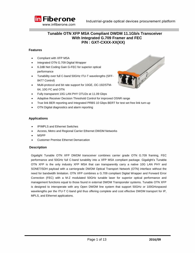
Page 1 of 13 2016/09 Tunable OTN XFP MSA Compliant DWDM 11.1Gb/s Transceiver With Integrated G.709 Framer and FEC P/N : GXT-CXXX-XX(XX) Features Compliant with XFP MSA Integrated OTN G.709 Digital Wrapper 6.2dB Net Coding Gain G-FEC for superior optical performance Tunability over full C-band 50GHz ITU-T wavelengths (SFF- 8477 Control) Multi-protocol and bit rate support for 10GE, OC-192/STM- 64, 10G FC and OTN Fully transparent 10G LAN PHY OTU2e at 11.09 Gbps Adaptive Receiver Decision Threshold Control for improved OSNR range True link BER reporting and Integrated PRBS 10 Gbps BERT for test set free link turn-up OTN Digital diagnostics and alarm reporting Applications IP/MPLS and Ethernet Switches Access, Metro and Regional Carrier Ethernet DWDM Networks MSPP Customer Premise Ethernet Demarcation Description Gigalight Tunable OTN XFP DWDM transceiver combines carrier grade OTN G.709 framing, FEC performance and 50GHz full C-band tunability into a XFP MSA compliant package. Gigalight‟s Tunable OTN XFP is the only industry XFP MSA that can transparently carry a native 10G LAN PHY and SONET/SDH payload with a carriergrade DWDM Optical Transport Network (OTN) interface without the need for bandwidth limitation. OTN XFP combines a G.709 compliant Digital Wrapper and Forward Error Correction (FEC) with a M-Z modulated 50GHz tunable laser for superior optical performance and management functions equal to those found in external DWDM Transponder systems. Tunable OTN XFP is designed to interoperate with any Open DWDM line system that support 50GHz or 100GHzspaced wavelengths per the ITU-T C-band grid thus offering complete and cost effective DWDM transport for IP, MPLS, and Ethernet applications.
Transcript of Tunable OTN XFP MSA Compliant DWDM 11.1Gb/s · PDF fileTunable OTN XFP MSA Compliant DWDM...
Page 1 of 13 2016/09
Tunable OTN XFP MSA Compliant DWDM 11.1Gb/s Transceiver With Integrated G.709 Framer and FEC
P/N : GXT-CXXX-XX(XX)
Features
Compliant with XFP MSA
Integrated OTN G.709 Digital Wrapper
6.2dB Net Coding Gain G-FEC for superior optical
performance
Tunability over full C-band 50GHz ITU-T wavelengths (SFF-
8477 Control)
Multi-protocol and bit rate support for 10GE, OC-192/STM-
64, 10G FC and OTN
Fully transparent 10G LAN PHY OTU2e at 11.09 Gbps
Adaptive Receiver Decision Threshold Control for improved OSNR range
True link BER reporting and Integrated PRBS 10 Gbps BERT for test set free link turn-up
OTN Digital diagnostics and alarm reporting
Applications
IP/MPLS and Ethernet Switches
Access, Metro and Regional Carrier Ethernet DWDM Networks
MSPP
Customer Premise Ethernet Demarcation
Description
Gigalight Tunable OTN XFP DWDM transceiver combines carrier grade OTN G.709 framing, FEC
performance and 50GHz full C-band tunability into a XFP MSA compliant package. Gigalight‟s Tunable
OTN XFP is the only industry XFP MSA that can transparently carry a native 10G LAN PHY and
SONET/SDH payload with a carriergrade DWDM Optical Transport Network (OTN) interface without the
need for bandwidth limitation. OTN XFP combines a G.709 compliant Digital Wrapper and Forward Error
Correction (FEC) with a M-Z modulated 50GHz tunable laser for superior optical performance and
management functions equal to those found in external DWDM Transponder systems. Tunable OTN XFP
is designed to interoperate with any Open DWDM line system that support 50GHz or 100GHzspaced
wavelengths per the ITU-T C-band grid thus offering complete and cost effective DWDM transport for IP,
MPLS, and Ethernet applications.

Page 2 of 13 2016/09
Tunable OTN XFP G.709 digital wrapper overhead and FEC functions are handled by the OTN Processor,
which is integrated into the XFP module. The OTN Processor provides Operations Administration and
Management (OAM) functions with G.709 alarms and Performance Management statistics.
Management
Management of the Tunable OTN XFP is provided via the XFP MSA I2C interface, which supports digital diagnostic
monitoring, alarms and loop backs to include G.709 and FEC management registers and wavelength tuning. Routers
and Switches can reap the performance gains of FEC without changes to the existing I2C interface in a management
Transparent Mode of operation, in which the Tunable OTN XFP activates the G.709 Digital Wrapper an FEC coding
without the need for specific I2C provisioning.
Tunable OTN XFP MSA Compliant DWDM 10Gb/s Transceiver with Integrated G.709 and FEC Transceiver Optical Specifications (G.709 and FEC Enabled)
Parameter Symbol Min Typical Max Units
Host Native Nominal Bit Rate 9.9533 (SONET/SDH)
10.3125 (LAN PHY)
Gbps
DWDM Line Interface Bit Rate
10.7092 (OTU2)
11.049 (OTU1e LAN PHY)
11.0957 (OTU2e LAN PHY)
Gbps
OTN Interface Bit Rate
Deviation
+/- 20 (SONET)
+/- 100 (LAN PHY) ppm
DWDM Wavelength Range λWDM 1528.38 - 1565.50 nm
Channel Spacing fSPACING 50 GHz
Laser Tuning Range fTUNE Full C-band
Wavelength Accuracy
λEOL -25 - +25 pm
Extinction Ratio ER 9 - - dB
XFI Electrical
InterfaceOUT-2
DWDM
I2C
Mgmt IntI2C Int
OTN Tx Processor
FEC Encoder
G.709 Framer/Processor
Tunable 50GHz
Laser/ M-Z
Mod
OTN Rx Processor
G.709 Framer/Processor
FEC Decoder
APD or PIN Rx

Page 3 of 13 2016/09
Side Mode Suppression Ratio SMSR 30 - - dB
Average Output Power POUT 0 - +3 dBm
Eye Mask Compliance GR-253i3/G.959.1
Receiver Operating Range @
11.1Gbps
0ps/nm Dispersion
+1400ps/nm Dispersion
PIN
(80km APD)
-28
-25
-
-
-7
-7
dBm
dBm
Receiver Operating Range @
11.1Gbps
0ps/nm Dispersion
+1400ps/nm Dispersion
PIN
(40km PIN)
-18
-16
-
-
0
-2
dBm
dBm
OSNR Requirement @
11.1Gbps
0 ps/nm
-500ps/nm to +1300ps/nm
Dispersion
-18dBm to -8dBm Input
OSNRMIN
(80km APD)
16
20
-
-
-
-
dB/
0.1nm
OSNR Requirement @
11.1Gbps
0 ps/nm
+800ps/nm Dispersion
-12dBm to -1dBm Input
OSNRMIN
(40km PIN)
15.5
19
-
-
-
-
dB/
0.1nm
Jitter Compliance - 802.3ae/GR-253i3
Operating Case Temperature TC -5 - 70 °C
Storage Temperature Tstg -40 - 85 °C

Page 4 of 13 2016/09
PRBS-31 “True Link” Pattern Generator and Checker
The OTN XFP “True Link” feature consists of a PRBS-31 Generator and Checker to allow the customer to determine
the 11Gbps channel performance without the need for costly 10GE or OC-192 payload test equipment. In the
transmit direction a PRBS-31 pattern is generated and inserted into the OTU-2 payload portion of the frame. The
OTU-2, ODU-2 and FEC data is generated and monitored normally to allow for link alarming and FEC correction
performance monitoring. A status bit it provided to the user to denote PRBS-31 pattern synchronization. In the
receive direction, the PRBS-31 payload is decoded and checked for individual bit level errors. A PRBS-31 payload
error counter is provided via the OTN XFP standard I2C interface.
The following I2C registers are used for the True Link feature:
Page Reg Bit Type Title
Description Settings
03h 183 7 R/W, SC
PRBS31 Control (Line Side)
PRBS-31 error counter reset (Self Clearing Bit)
1 = Reset PRBS-31 error counter (This bit is self clearing back to zero) 0 = Normal operation.
03h 183 5:6 R/W Reserved
03h 183 4 RO PRBS31 sync status
0 = PRBS-31 Rx pattern sync present 1 = PRBS-31 Rx pattern sync error
03h 183 2:3 R/W Reserved
03h 183 1 R/W Enable PRBS31 pattern on Rx Path
1 = Enable PRBS31 payload read in the Rx direction. If FEC enabled, PRBS31 is error corrected. If FEC is off, PRBS1 raw data is sent. 0 = Disable PRBS31 payload read in the Rx direction.
03h 183 0 R/W Enable PRBS31 pattern on Tx Path
1 = Enable PRBS31 payload insertion in the Tx direction. The Tx direction PRBS data is inserted as the payload data in the OTU2 frame. 0 = Disable PRBS31 payload insertion in the Rx direction.
Page Reg Bit Type Title
Description Settings
03h 184 7:0 RO
PRBS31 Checker
(Line Side)
PRBS31 Error Counter (MSB- 32 bit counter)
PRBS31 Error Count (MSB- 32 bit)
03h 185 7:0 RO PRBS31 Error Counter (17 to 24 of 32 bit counter)
PRBS31 Error Count (17 to 24 of 32 bit counter).
03h 186 7:0 RO PRBS31 Error Counter (8 to 16 of 32 bit counter)
PRBS31 Error Count (8 to 16 of 32 bit counter)
03h 187 7:0 RO PRBS31 Error Counter (LSB- 32 bit counter)
PRBS31 Error Count (LSB- 32 bit).

Page 5 of 13 2016/09
Link Checker Feature
The OTN XFP has the optional “Link Checker” feature, allowing the customer to proactively monitor the link
performance margin in real time locally or remotely. Link Checker provides proactive alarms to alert the customer of
a link falling below a pre-defined margin threshold, triggering an investigation of the optical layer to rectify the
degradation before the customer takes errors. The user monitors Laser Bias Current to verify the health or margin on
the OTN wavelength. The Link Checker margin can vary between 3 and 12, in which the higher the number the
higher the margin. This is illustrated in the graph below.
As seen an OTN XFP DWDM channel with a Link Checker reading of 6 or higher is operating with a good operating
margin. Between 4 and 6 the link margin is low and may be the indicator of a link problem on the DWDM system. At
4 or below traffic is affected or down on that link.
The link margin is supported through the reading of the FEC Correction Error Rate (FCER) in the XFP and displaying
that margin as the Laser Bias Current value on the router. The FEC correction error rate is averaged over a 25
second rolling window by the module software. In the case of failure or no errors being corrected, the correction error
rate is shown as 12.
The transposition of the correction error rate to laser bias current is shown below:
The FEC Correction BER can be represented as:
xx = Mantissa yy = Exponent
For example, an error correction error rate of 3x10⁻⁶
where the Mantissa xx = 3 and the Exponent yy = 6
The Laser Bias Current on the router is then shown as = yy.xx mA
Therefore a FEC Correction Error Rate (FCER) of 3x10⁻⁶
is shown as a Laser Bias current of 6.3 mA
Any error rate <10-5 will raise a Laser Bias Low Alarm in the system, which is an early warning indicator to the NOC
to proactively monitor and correct for a degraded link before errors are seen by the customer.

Page 6 of 13 2016/09
OTN XFP Loopbacks OTN XFP supports both host and line loopbacks. The host loopback is designed to loopback traffic towards the host before processing by the FEC and G.709 overhead processor in the OTN XFP module. A line loopback loops the traffic towards the OTN fiber network before processing the FEC and G.709 overhead. Both loopbacks are completed in the FEC/G.709 ASIC. All loopbacks are supported via the I2C interface. The following loopbacks are supported:
1. Host Loopback (towards host). This is referred to as the XFI loopback in the XFF MSA Rev 4.5.
2. Line Loopback (towards OTN fiber network)
OTN XFP
Laser
Modulator
Receiver/TIA
FEC Encoder/Decoder
G.709 OverheadXFI1 2
The XFP loopback settings are controlled according to the MSA XFP I2C interface using the following registers:
Table Reg Bits Type Category Register Item Feature Notes
Any 1 2 R/W Signal Conditioner
Line Side Loopback
0 = Normal Operation
1 = Loopback Module Optical Input to Output
Any 1 1 XFI Loopback
0 = Normal Operation
1 = Loopback Module XFI Input to Output

Page 7 of 13 2016/09
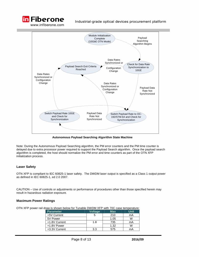
Startup Autonomous Payload Searching OTN XFP supports a payload search feature when the module is initially powered up or reset. The Payload Search feature is only valid in OTN mode and is run to select the correct payload data rate for the module if the host does not select the value in the XFP Signal Conditioner register. Since the OTN XFP contains PLLs and reference clocks centered on the exact OTN output bit rate, the module must be configured in the correct payload bit rate mode for proper operation. A module not configured correctly cannot pass traffic. The Payload Search mode works in the following steps:
1. Upon module initialization or reset completion, the module default configuration is 10GE LAN PHY (10.3125Gbps) with OTN enabled (11.1Gbps). When the module exists the initialization stage, an internal check is performed on the incoming host side data to see if the payload data rate matches the configured 10GE (10.3125Gbps) data rate.
2. If the module is not able to synchronize to the default configuration data rate of 10GE (10.3125Gbps) with the incoming host data, the module is automatically configured by the firmware to a data rate of OC-192/STM-64 (9.953Gbps) and timing synchronization is checked again.
3. If after step 2 the data rate of the incoming host data is not synchronized to the payload data rate, the module will continue switching between 10GE and OC-192/STM-64 data rates until a synchronization of payload data rate occurs. The time between switches is about 5 seconds. If no input electrical XFI signal is present on the host input side, the Payload Searching algorithm is frozen and resumed when data is detected.
4. If at any time during Step 1. through Step 3. the payload data is correctly synchronized to the module settings, the Autonomous Payload Searching loop is exited. During the Payload Searching algorithm the laser output is disabled and the module is held in a MOD_NR state. The data rate setting of the Signal Conditioner register [1.7:4] will display the OTN XFP current payload data rate setting.
The following conditions force the module to exit the Autonomous Payload Searching algorithm:
Autonomous Payload Search Exit Criteria
Condition Description Notes
Host Payload Sync to Module Settings
The host input electrical XFI data rate matches the module payload data rate configuration
Host data must be present
Signal Conditioner Register is written Lower Memory Register 1 is written
Signifies host is writing data rate value in I2C
Register
OTN Setup Register 1 is written Register [03,128] is written
Signifies host is writing OTN configuration
change, which can affect data rate
Payload Search is Disabled Register [03,192.2] is written to „0‟
Host disabled the Payload Search via I2C
The following state diagram explains the Autonomous Payload Search operation:
Page 8 of 13 2016/09
Module Initialization
Complete
(10GbE OTN Mode)
Check for Data Rate
Synchronization to
10GE
Payload
Searching
Algorithm Begins
Switch Payload Rate to OC-
192/STM-64 and Check for
Synchronization
Switch Payload Rate 10GE
and Check for
Synchronization
Payload Data
Rate Not
Synchronized
Payload Data
Rate Not
Synchronized
Payload Search Exit Criteria
Reached
Data Rates
Synchronized or
Configuration
Change
Data Rates
Synchronized or
Configuration
Change Data Rates
Synchronized or
Configuration
Change
Autonomous Payload Searching Algorithm State Machine
Note: During the Autonomous Payload Searching algorithm, the PM error counters and the PM time counter is delayed due to extra processor power required to support the Payload Search algorithm. Once the payload search algorithm is completed, the host should normalize the PM error and time counters as part of the OTN XFP initialization process.
Laser Safety OTN XFP is compliant to IEC 60825-1 laser safety. The DWDM laser output is specified as a Class 1 output power as defined in IEC 60825-1, ed 2.0 2007.
CAUTION – Use of controls or adjustments or performance of procedures other than those specified herein may result in hazardous radiation exposure. Maximum Power Ratings OTN XFP power rail draw is shown below for Tunable DWDM XFP with 70C case temperature:
Parameter Voltage Max Unit
+5V Current 5 210 mA
5V Power 1.05 W
+1.8V Current 1.8 735 mA
+1.8V Power 1.32 W
+3.3V Current 3.3 575 mA

Page 9 of 13 2016/09
+3.3V Power 1.90 W
Total Module Power 4.27 W
DOM Alarm Thresholds and I2C Locations
All Alarm Thresholds for OTN XFP are configured at the manufacturer and cannot be configured through the I2C
interface (i.e. thresholds are not provisionable).Alarm thresholds for each DOM parameter are located in the following
registers.
Threshold
Value
Register
Latched
Alarm
Threshold
Size
(Bytes)
Name
02-03 80.7 2 Transceiver Temp High Alarm
04-05 80.6 2 Transceiver Temp Low Alarm
06-07 82.7 2 Transceiver Temp High Warning
08-09 82.6 2 Transceiver Temp Low Warning
10-17 N/A 8 Reserved
18-19 80.3 2 Laser Bias Current High Alarm
20-21 80.2 2 Laser Bias Current Low Alarm
22-23 82.3 2 Laser Bias Current High Warning
24-25 82.2 2 Laser Bias Current Low Warning
26-27 80.1 2 Laser Output Power High Alarm
28-29 80.0 2 Laser Output Power Low Alarm
30-31 82.1 2 Laser Output Power High Warning
32-33 82.0 2 Laser Output Power Low Warning
34-35 81.7 2 Receive Optical Power High Alarm
36-37 81.6 2 Receive Optical Power Low Alarm
38-39 83.7 2 Receive Optical Power High Warning
40-41 83.6 2 Receive Optical Power Low Warning
N/A
86.7
N/A
5V High Alarm
86.6 5V Low Alarm
86.5 3.3V High Alarm
86.4 3.3V Low Alarm
86.3 1.8V High Alarm
86.2 1.8V Low Alarm
86.1 -5V High Alarm (Not Used)
86.0 -5V Low Alarm (Not Used)
87.7 5V High Warning
87.6 5V Low Warning
87.5 3.3V High Warning
87.4 3.3V Low Warning
87.3 1.8V High Warning
87.2 1.8V Low Warning

Page 10 of 13 2016/09
Threshold
Value
Register
Latched
Alarm
Threshold
Size
(Bytes)
Name
87.1 -5V High Warning (Not Used)
87.0 -5V Low Warning (Not Used)
Host Connector Specifications
The XFP PCB host electrical connections are shown in the figure below.

Page 11 of 13 2016/09
XFP PCB Electrical Connections
Pin No Name Logic Function Notes
1 GND Electrical Ground 1
2 VEE5 Optional -5.2V power Supply (Not used)
3 Mod_DeSel LVTTL-I Module De-select; When held low allows module to respond to 2-wire serial interface
4 Interrupt LVTTL-O Interrupt; Indicates presence of an important condition which can be read over the 2-wire serial interface
2
5 Tx_DIS LVTTL-I Transmitter Disable; Turns off transmitter laser output
6 VCC5 +5V Power Supply
7 GND Module Ground 1
8 VCC3 +3.3V Power Supply
9 VCC3 +3.3V Power Supply
10 SCL LVTTL-I/O 2-Wire Serial Interface Clock 2
11 SDA LVTTL-I/O 2-Wire Serial Interface Data Line 2
12 Mod_Abs LVTTL-O Indicates Module is not present. Grounded in the Module 2
13 Mod_NR LVTTL-O Module Not Ready; Indicating Module Operational Fault 2
14 RX_LOS LVTTL-O Receiver Loss Of Signal Indicator 2
15 GND Module Ground 1
16 GND Module Ground 1
17 RD- CML-O Receiver Inverted Data Output
18 RD+ CML-O Receiver Non-Inverted Data Output
19 GND Module Ground 1
20 VCC2 +1.8V Power Supply 3
21 P_Down/RST LVTTL-I Power down; When high, requires the module to limit power consumption. 2-Wire serial interface must be functional in the low power mode.
Reset; The falling edge initiates a complete reset of the module including the 2-wire serial interface, equivalent to a power cycle.
22 VCC2 +1.8V Power Supply 3
23 GND Module Ground 1
24 RefCLK+ PECL-I Reference Clock Non-Inverted Input, AC coupled on the host board
25 RefCLK- PECL-I Reference Clock Inverted Input, AC coupled on the host board
26 GND Module Ground 1
27 GND Module Ground 1
28 TD- CML-I Transmitter Inverted Data Input
29 TD+ CML-I Transmitter Non-Inverted Data Input
30 GND Module Ground 1
Notes: 1. Module ground pins (GND) are isolated from the module case and chassis ground within the module. 2. Shall be pulled up with 4.7K-10K ohms to a voltage between 3.15V and 3.45V on the host board.
Page 12 of 13 2016/09
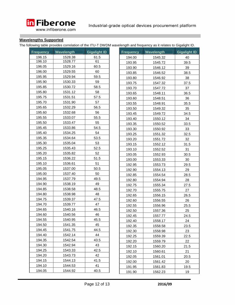
Wavelengths Supported The following table provides correlation of the ITU-T DWDM wavelength and frequency as it relates to Gigalight ID.
Frequency Wavelength Gigalight ID
196.15 1528.38 61.5
196.10 1528.77 61
196.05 1529.16 60.5
196.00 1529.55 60
195.95 1529.94 59.5
195.90 1530.33 59
195.85 1530.72 58.5
195.80 1531.12 58
195.75 1531.51 57.5
195.70 1531.90 57
195.65 1532.29 56.5
195.60 1532.68 56
195.55 1533.07 55.5
195.50 1533.47 55
195.45 1533.86 54.5
195.40 1534.25 54
195.35 1534.64 53.5
195.30 1535.04 53
195.25 1535.43 52.5
195.20 1535.82 52
195.15 1536.22 51.5
195.10 1536.61 51
195.05 1537.00 50.5
195.00 1537.40 50
194.95 1537.79 49.5
194.90 1538.19 49
194.85 1538.58 48.5
194.80 1538.98 48
194.75 1539.37 47.5
194.70 1539.77 47
194.65 1540.16 46.5
194.60 1540.56 46
194.55 1540.95 45.5
194.50 1541.35 45
194.45 1541.75 44.5
194.40 1542.14 44
194.35 1542.54 43.5
194.30 1542.94 43
194.25 1543.33 42.5
194.20 1543.73 42
194.15 1544.13 41.5
194.10 1544.53 41
194.05 1544.92 40.5
Frequency Wavelength Gigalight ID
194.00 1545.32 40
193.95 1545.72 39.5
193.90 1546.12 39
193.85 1546.52 38.5
193.80 1546.92 38
193.75 1547.32 37.5
193.70 1547.72 37
193.65 1548.11 36.5
193.60 1548.51 36
193.55 1548.91 35.5
193.50 1549.32 35
193.45 1549.72 34.5
193.40 1550.12 34
193.35 1550.52 33.5
193.30 1550.92 33
193.25 1551.32 32.5
193.20 1551.72 32
193.15 1552.12 31.5
193.10 1552.52 31
193.05 1552.93 30.5
193.00 1553.33 30
192.95 1553.73 29.5
192.90 1554.13 29
192.85 1554.54 28.5
192.80 1554.94 28
192.75 1555.34 27.5
192.70 1555.75 27
192.65 1556.15 26.5
192.60 1556.55 26
192.55 1556.96 25.5
192.50 1557.36 25
192.45 1557.77 24.5
192.40 1558.17 24
192.35 1558.58 23.5
192.30 1558.98 23
192.25 1559.39 22.5
192.20 1559.79 22
192.15 1560.20 21.5
192.10 1560.61 21
192.05 1561.01 20.5
192.00 1561.42 20
191.95 1561.83 19.5
191.90 1562.23 19

Page 13 of 13 2016/09
Frequency Wavelength Gigalight ID
191.85 1562.64 18.5
191.80 1563.05 18
191.75 1563.45 17.5
191.70 1563.86 17
191.65 1564.27 16.5
Frequency Wavelength Gigalight ID
191.60 1564.68 16
191.55 1565.09 15.5
191.50 1565.50 15
Ordering Guide The OTN XFP part number is shown below.
Part Number Examples are shown below:
Part Number Feature Description
GXT-CXXX-80A OTN XFP, Full C-band Tunable, OTN OTU2 Integrated Framer with G.975 FEC, Link Checker Feature Enabled, ITU-T Channel 16.0 Default Wavelength, APD Receiver
GXT-CXXX-00A OTN XFP, Full C-band Tunable, OTN OTU2 Integrated Framer with G.975 FEC, ITU-T Channel 16.0 Default Wavelength, APD Receiver
GXT-CXXX-80P OTN XFP, Full C-band Tunable, OTN OTU2 Integrated Framer with G.975 FEC, Link Checker Feature Enabled, ITU-T Channel 16.0 Default Wavelength, PIN Receiver
Important Notice
Performance figures, data and any illustrative material provided in this data sheet are typical and
must be specifically confirmed in writing by GIGALIGHT before they become applicable to any
particular order or contract. In accordance with the GIGALIGHT policy of continuous improvement
specifications may change without notice. The publication of information in this data sheet does not
imply freedom from patent or other protective rights of GIGALIGHT or others. Further details are
available from any GIGALIGHT sales representative.
E-mail: Business Inquiry: [email protected] Customer Support: [email protected] Account Issue: [email protected] Suggestion/advice: [email protected]