Tunable Fröhlich Polarons in Organic Single-Crystal ... polar dielectric the role of Fröhlich ......
25
Tunable Fröhlich Polarons in Organic Single-Crystal Transistors I. N. Hulea 1 , S. Fratini 2 , H. Xie 1 , C.L. Mulder 1 , N.N. Iossad 1 , G. Rastelli 2,3 , S. Ciuchi 3 , and A. F. Morpurgo 1 1 Kavli Institute of Nanoscience, Delft University of Technology, Lorentzweg 1, 2628 CJ Delft, The Netherlands 2 Laboratoire d’Etudes des Propriétés Electroniques des Solides, CNRS, BP 166 - 25, Avenue des Martyrs, F-38042 Grenoble Cedex 9, France 3 INFM-CNR SMC and Dipartimento di Fisica, Università dell’Aquila, via Vetoio, I- 67010 Coppito-L’Aquila, Italy
Transcript of Tunable Fröhlich Polarons in Organic Single-Crystal ... polar dielectric the role of Fröhlich ......
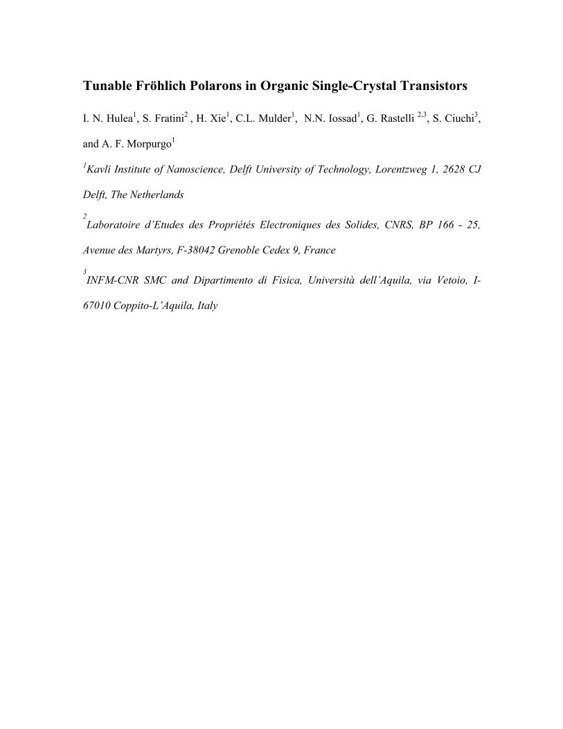
Tunable Fröhlich Polarons in Organic Single-Crystal Transistors
I. N. Hulea1, S. Fratini2 , H. Xie1, C.L. Mulder1, N.N. Iossad1, G. Rastelli 2,3, S. Ciuchi3,
and A. F. Morpurgo1
1Kavli Institute of Nanoscience, Delft University of Technology, Lorentzweg 1, 2628 CJ
Delft, The Netherlands
2
Laboratoire d’Etudes des Propriétés Electroniques des Solides, CNRS, BP 166 - 25,
Avenue des Martyrs, F-38042 Grenoble Cedex 9, France
3
INFM-CNR SMC and Dipartimento di Fisica, Università dell’Aquila, via Vetoio, I-
67010 Coppito-L’Aquila, Italy
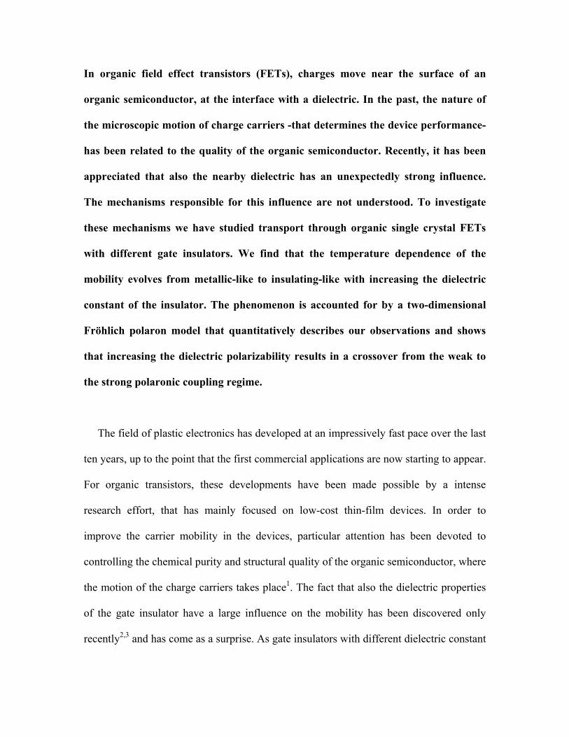
In organic field effect transistors (FETs), charges move near the surface of an
organic semiconductor, at the interface with a dielectric. In the past, the nature of
the microscopic motion of charge carriers -that determines the device performance-
has been related to the quality of the organic semiconductor. Recently, it has been
appreciated that also the nearby dielectric has an unexpectedly strong influence.
The mechanisms responsible for this influence are not understood. To investigate
these mechanisms we have studied transport through organic single crystal FETs
with different gate insulators. We find that the temperature dependence of the
mobility evolves from metallic-like to insulating-like with increasing the dielectric
constant of the insulator. The phenomenon is accounted for by a two-dimensional
Fröhlich polaron model that quantitatively describes our observations and shows
that increasing the dielectric polarizability results in a crossover from the weak to
the strong polaronic coupling regime.
The field of plastic electronics has developed at an impressively fast pace over the last
ten years, up to the point that the first commercial applications are now starting to appear.
For organic transistors, these developments have been made possible by a intense
research effort, that has mainly focused on low-cost thin-film devices. In order to
improve the carrier mobility in the devices, particular attention has been devoted to
controlling the chemical purity and structural quality of the organic semiconductor, where
the motion of the charge carriers takes place1. The fact that also the dielectric properties
of the gate insulator have a large influence on the mobility has been discovered only
recently2,3 and has come as a surprise. As gate insulators with different dielectric constant
can result in devices exhibiting mobility values differing by more than one order of
magnitude, the fundamental understanding of this effect is now crucial for further
optimization of FET devices.
Our work relies on temperature-dependent electrical transport measurements through
rubrene single-crystal FETs. In contrast to thin-film devices, recent experiments have
demonstrated that the influence of disorder on transport in these single-crystal transistors
is negligible4-6 near room-temperature. So far, however, these experiments have not yet
given precise indications as to the microscopic nature of charge carriers at
organic/dielectric interfaces. Most theories developed to describe transport in organic
crystals have considered the possibility that charge carriers behave as Holstein polarons,
i.e. quasiparticles formed by a charge carrier bound to a short-range deformation of the
molecular crystal7. The formation of Fröhlich polarons —quasiparticles consisting of a
charge carrier bound to an ionic polarization cloud in the surrounding medium— has
received much less attention, because it is not expected to occur in the bulk of organic
semiconductors. Nevertheless, in FETs, where charge carriers move at the interface with
a polar dielectric the role of Fröhlich polarons needs to be addressed8.
To address this issue, we have used rubrene single crystal FETs fabricated using
different techniques9, that enabled us to vary the dielectric constant of the gate insulator
from 1 to 25 (see Methods section). A total of more than 100 FETs were studied, in
which the gate dielectric was vacuum (g=1), parylene (g=2.9), SiO2 (g=3.9), Si
3N
4
(g=7.5), Al2O
3 (g=9.4), and Ta
2O
5 (g=25). Fig.1 (c) and (d) show two single crystal
rubrene devices. Examples of source-drain current versus gate voltage (ISD
-VG) curves
measured at different temperatures are shown in Fig. 1 (e) and (f) (all the measurements
presented in this paper have been performed along the high-mobility b-direction). From
these curves we extract the value of the carrier mobility from the linear regime, and of the
threshold voltage VTH
, by extrapolating the linear part of the ISD
-VG curve to zero current.
Measurements were performed in between 300 K and 200 K. Below this temperature the
difference between the thermal expansion of the organic material and of their supporting
substrates often causes device failure due to the formation of crack in the crystals. In the
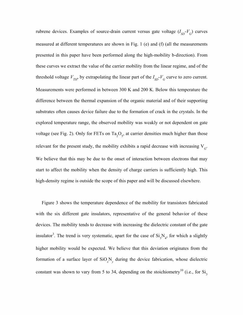
explored temperature range, the observed mobility was weakly or not dependent on gate
voltage (see Fig. 2). Only for FETs on Ta2O
5, at carrier densities much higher than those
relevant for the present study, the mobility exhibits a rapid decrease with increasing VG.
We believe that this may be due to the onset of interaction between electrons that may
start to affect the mobility when the density of charge carriers is sufficiently high. This
high-density regime is outside the scope of this paper and will be discussed elsewhere.
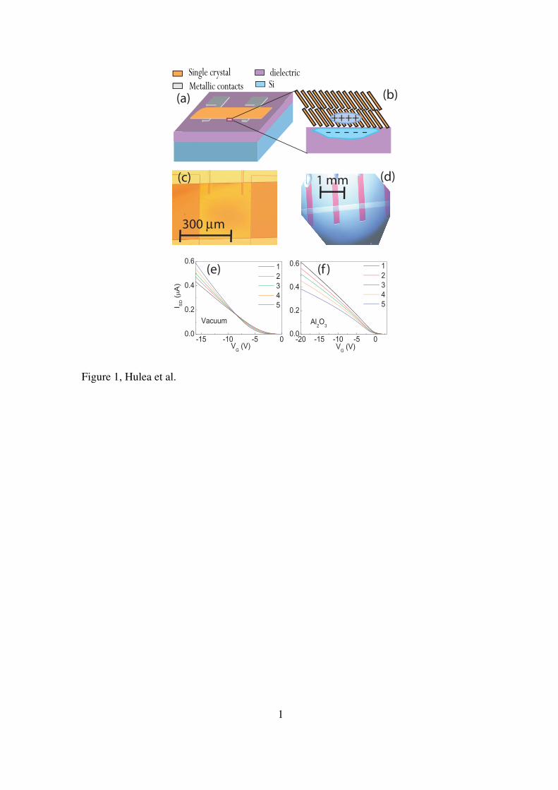
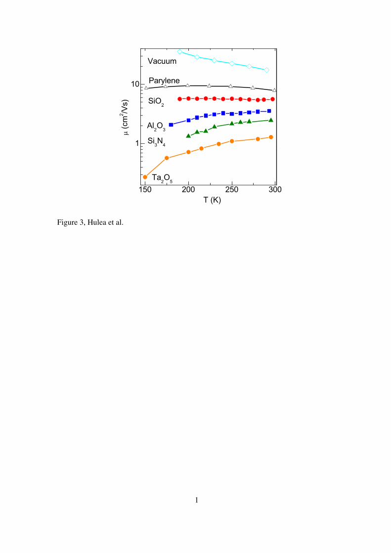
Figure 3 shows the temperature dependence of the mobility for transistors fabricated
with the six different gate insulators, representative of the general behavior of these
devices. The mobility tends to decrease with increasing the dielectric constant of the gate
insulator3. The trend is very systematic, apart for the case of Si3N
4, for which a slightly
higher mobility would be expected. We believe that this deviation originates from the
formation of a surface layer of SiOxN
y during the device fabrication, whose dielectric
constant was shown to vary from 5 to 34, depending on the stoichiometry10 (i.e., for Si3
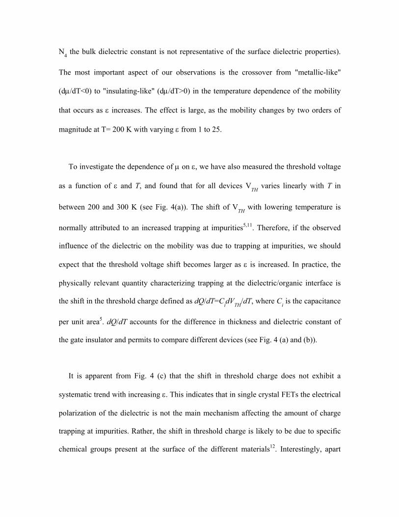
N4 the bulk dielectric constant is not representative of the surface dielectric properties).
The most important aspect of our observations is the crossover from "metallic-like"
(do/dT<0) to "insulating-like" (do/dT>0) in the temperature dependence of the mobility
that occurs as g increases. The effect is large, as the mobility changes by two orders of
magnitude at T= 200 K with varying g from 1 to 25.
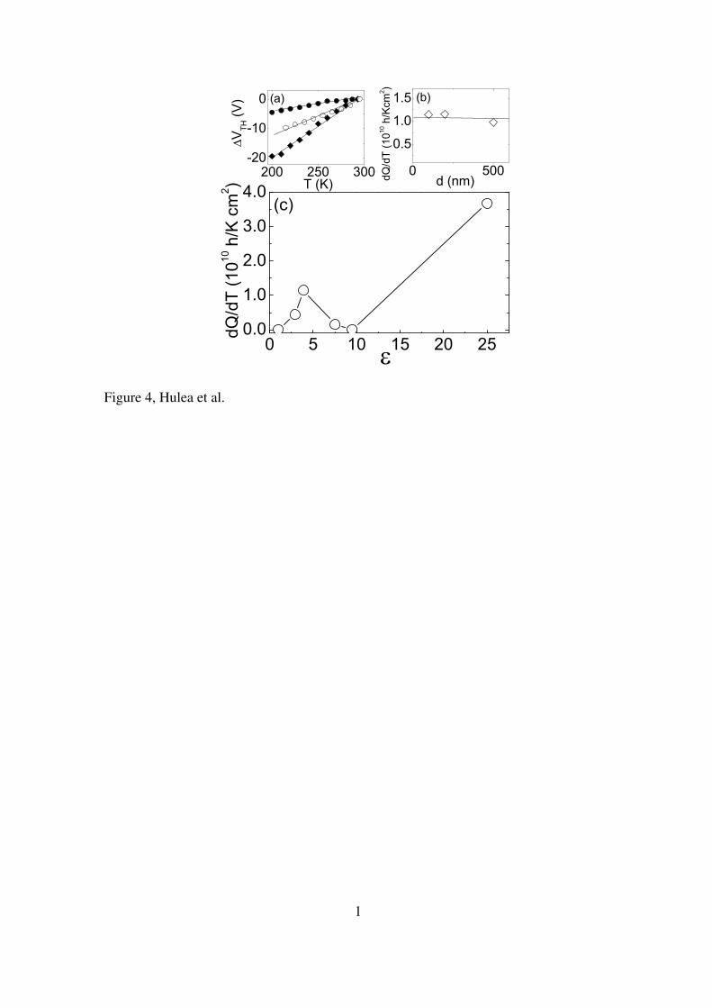
To investigate the dependence of o on g, we have also measured the threshold voltage
as a function of g and T, and found that for all devices VTH
varies linearly with T in
between 200 and 300 K (see Fig. 4(a)). The shift of VTH
with lowering temperature is
normally attributed to an increased trapping at impurities5,11. Therefore, if the observed
influence of the dielectric on the mobility was due to trapping at impurities, we should
expect that the threshold voltage shift becomes larger as g is increased. In practice, the
physically relevant quantity characterizing trapping at the dielectric/organic interface is
the shift in the threshold charge defined as dQ/dT=CidV
TH/dT, where C
i is the capacitance
per unit area5. dQ/dT accounts for the difference in thickness and dielectric constant of
the gate insulator and permits to compare different devices (see Fig. 4 (a) and (b)).
It is apparent from Fig. 4 (c) that the shift in threshold charge does not exhibit a
systematic trend with increasing g. This indicates that in single crystal FETs the electrical
polarization of the dielectric is not the main mechanism affecting the amount of charge
trapping at impurities. Rather, the shift in threshold charge is likely to be due to specific
chemical groups present at the surface of the different materials12. Interestingly, apart
from the case of Ta2O
5, the shift in threshold charge is highest for devices fabricated on
SiO2, which is one of the dielectrics most commonly used in the characterization of
organic thin film transistors. More importantly, the absence of a systematic trend between
threshold voltage and g implies that the dependence of o on g does not originate from
trapping of charge carriers. This is consistent with recent measurements of Hall effect
performed on rubrene single crystal FETs with vacuum, parylene6 and SiO2
13 gate
insulators, in which it was shown that in a range of temperatures between 200 and 300 K
the mobility obtained from FET measurements does indeed correspond to the intrinsic
(Hall) mobility. We conclude that the effect of the dielectric constant of the gate insulator
on the mobility of charge carriers is an intrinsic property of dielectric/organic interfaces.
The identification of an intrinsic dependence of the mobility on the dielectric
properties of the gate insulator suggests that the observed phenomenon originates from
the interaction of the charge carriers with their polar environment. Such an interaction is
well-known in condensed matter physics. In its essence it can be described by a Fröhlich
hamiltonian, in which free electrons interact with a dispersionless optical phonon of
characteristic frequency ys. In common inorganic semiconductors (e.g., Si or GaAs), the
effective strength of this interaction is weak due to both the low ionic polarizabilities and
the large bandwidths (low band masses) in these materials. As a consequence, the
coupling between the carriers and the polar degrees of freedom only causes a small
renormalization of the electronic properties. In organic transistors, on the other hand, the
bands are narrow (band masses are high) owing to the weak van der Waals bonding of
organic crystals, and the use of gate dielectrics with increasing ionic polarizabilities
permits to tune the strength of the interaction from the weak to the strong coupling
regime. In the latter case, the charge carriers form dielectric polarons. When the polaron
radius becomes comparable with the lattice spacing, transport close to room temperature
occurs through incoherent hopping between neighboring molecules. It follows that at
strong coupling the temperature dependence of the mobility changes from metallic-like to
thermally activated. This crossover to the strong coupling regime is the scenario that we
invoke to explain the experimental observations.
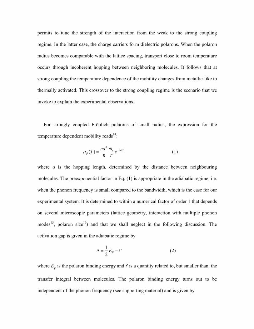
For strongly coupled Fröhlich polarons of small radius, the expression for the
temperature dependent mobility reads14:
2/( ) Ts
P
eaT
T
yo /F?
¥e (1)
where a is the hopping length, determined by the distance between neighbouring
molecules. The preexponential factor in Eq. (1) is appropriate in the adiabatic regime, i.e.
when the phonon frequency is small compared to the bandwidth, which is the case for our
experimental system. It is determined to within a numerical factor of order 1 that depends
on several microscopic parameters (lattice geometry, interaction with multiple phonon
modes15, polaron size16) and that we shall neglect in the following discussion. The
activation gap is given in the adiabatic regime by
1
'2
PE tF ? / (2)
where EP is the polaron binding energy and t' is a quantity related to, but smaller than, the
transfer integral between molecules. The polaron binding energy turns out to be
independent of the phonon frequency (see supporting material) and is given by
[BP
aE R
zd? ]yd (3)
where z is the distance between the polaron, located in the uppermost one or two
molecular layers of the crystal, and the surface of the dielectric. ( )(
s
s )
g gd
m g m g¢
¢
/?
- -
,s
is a
known parameter that quantifies the ionic polarizability of the interface, expressed in
terms of the measured dielectric constants of the gate dielectric (g g¢ ) and of rubrene
(m)17. aB=0.53Å is the Bohr radius.
In order to compare the experimental curves with Eq. 1 we isolate the part of the
temperature dependence of the mobility that is caused by the interaction of the charge
carriers with the polarizability of the dielectric. In fact, the o(T) curves measured
experimentally also include a contribution to the temperature dependence due to
mechanisms other than Fröhlich polarons, such as the coupling with the molecular
vibrations in the organic crystal. The contribution of these other effects can be
determined, as they are entirely responsible for the temperature dependence of the
mobility measured in FET in which the gate insulator is vacuum: obviously, for these
devices the polarizability of the gate dielectric does not play any role. In practice, we use
Matthiessen rule 1 1 1
( ) ( ) ( )P RT To o o? -
(P T
T as the simplest scheme to decouple the
Fröhlich contribution to the mobility )o , where oR(T) is the temperature dependent
mobility measured on FETs with vacuum as gate insulator.
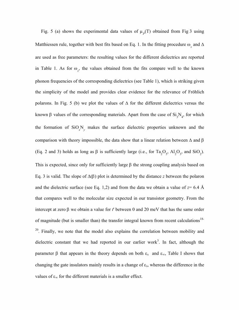
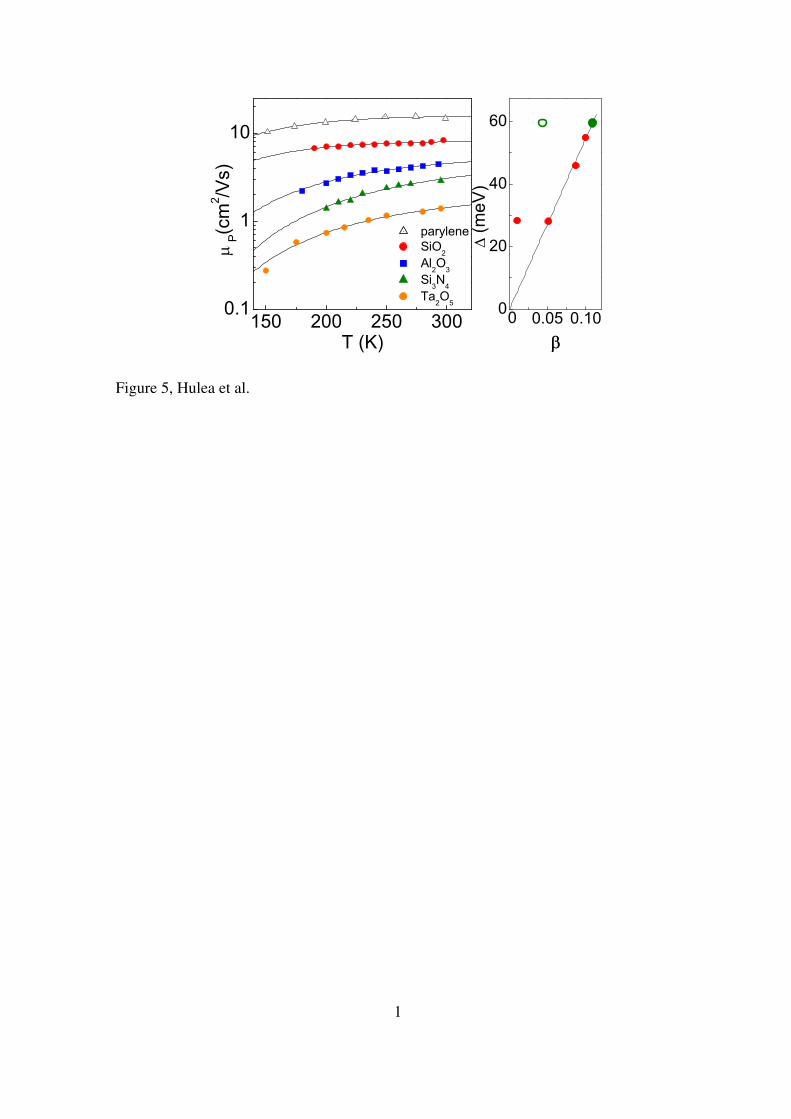
Fig. 5 (a) shows the experimental data values of oP(T) obtained from Fig 3 using
Matthiessen rule, together with best fits based on Eq. 1. In the fitting procedure ys and F
are used as free parameters: the resulting values for the different dielectrics are reported
in Table 1. As for ys, the values obtained from the fits compare well to the known
phonon frequencies of the corresponding dielectrics (see Table 1), which is striking given
the simplicity of the model and provides clear evidence for the relevance of Fröhlich
polarons. In Fig. 5 (b) we plot the values of F for the different dielectrics versus the
known d values of the corresponding materials. Apart from the case of Si3N
4, for which
the formation of SiOxN
y makes the surface dielectric properties unknown and the
comparison with theory impossible, the data show that a linear relation between F and d
(Eq. 2 and 3) holds as long as d is sufficiently large (i.e., for Ta2O
5, Al
2O
3, and SiO
2).
This is expected, since only for sufficiently large d the strong coupling analysis based on
Eq. 3 is valid. The slope of F(d) plot is determined by the distance z between the polaron
and the dielectric surface (see Eq. 1,2) and from the data we obtain a value of z= 6.4 Å
that compares well to the molecular size expected in our transistor geometry. From the
intercept at zero d we obtain a value for t' between 0 and 20 meV that has the same order
of magnitude (but is smaller than) the transfer integral known from recent calculations18-
20. Finally, we note that the model also explains the correlation between mobility and
dielectric constant that we had reported in our earlier work3. In fact, although the
parameter d that appears in the theory depends on both gs and gı, Table I shows that
changing the gate insulators mainly results in a change of gs, whereas the difference in the
values of gı for the different materials is a smaller effect.
The theoretical scenario that we have used works quantitatively because it specifically
accounts for the microscopic characteristics of the organic material -lattice periodicity
and narrow bandwidth- and of the gate dielectric -ionic polarisability and phonon
frequencies- that are all needed to give a consistent description of the experimental data.
The very good agreement between the values of ys obtained from the fits and the known
phonon frequencies of the corresponding dielectrics provides a direct demonstration of
this fact. To further validate this conclusion we have compared the experimental data to
predictions based on alternative models and found that they fail to give a consistent
interpretation. For instance, if the Fröhlich interaction is described in the usual
continuous medium approximation21, it is not possible to reproduce the thermally
activated behavior of the mobility, except at unrealistically large coupling strengths. We
have also analyzed the anti-adiabatic regime of the model discussed here, where the pre-
exponential factor does not depend on the phonon frequency ys, and found that in this
regime the results of the analysis are not internally consistent (see supplementary
material). Finding that the quality of the experimental data is sufficient to discriminate
between different microscopic models gives additional support to the conclusions
presented above.
We conclude that Fröhlich polarons are indeed formed in organic field-effect
transistors if the gate dielectric is sufficiently polar. This conclusion is important for
different reasons. First, it represents a considerable step forward in our basic
understanding of transport through organic transistors, as it identifies a microscopic
physical process that has a large influence on the device performance. Second, it shows
that dielectric/organic interfaces provide an ideal model system for the controlled study
of Fröhlich polarons, with tunable coupling. We emphasize that these conclusions have
been made possible by the high quality and reproducibility of recently developed organic
single crystal FETs. As the study of these devices has only started a few years ago, we
expect that future research on these systems will extend our fundamental knowledge of
electron transport in organic semiconductors by enabling reliable and systematic
measurements of many different quantities, such as electronic bandwidth, contact
resistance, low temperature transport. The resulting microscopic understanding will
permit to establish a solid scientific basis for the physics of organic semiconductors,
which will be crucial for future progress in the rapidly expanding field of plastic
electronics.
Methods
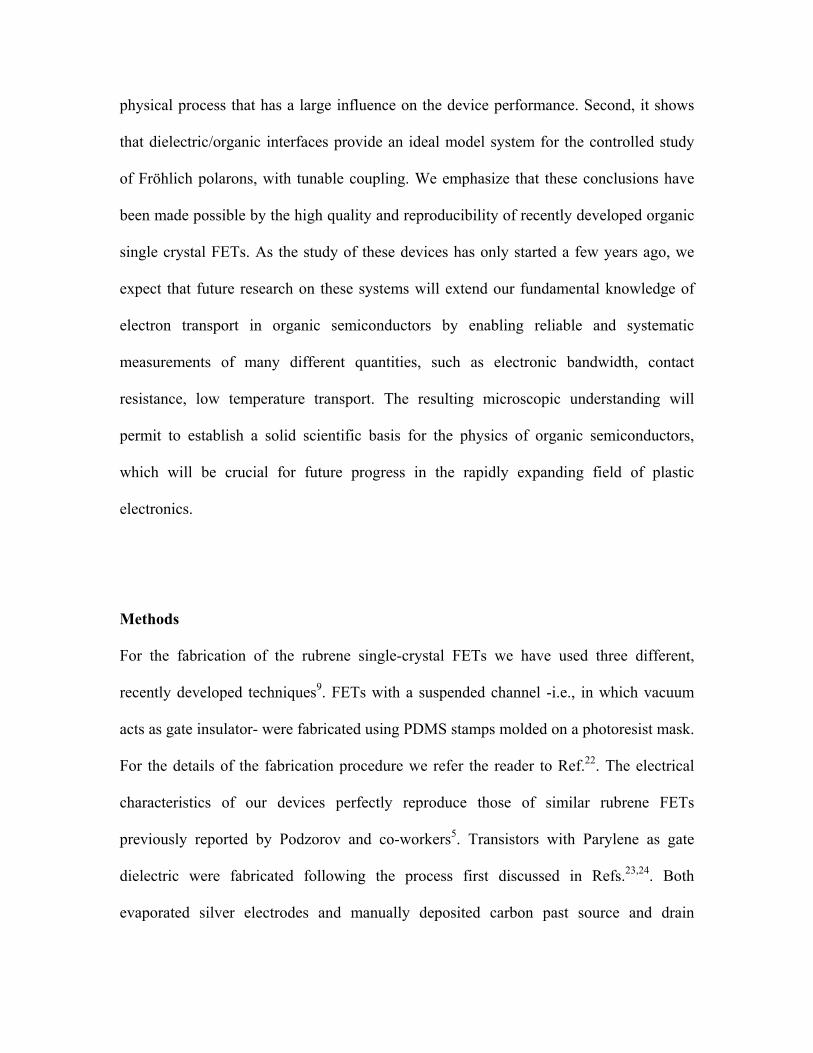
For the fabrication of the rubrene single-crystal FETs we have used three different,
recently developed techniques9. FETs with a suspended channel -i.e., in which vacuum
acts as gate insulator- were fabricated using PDMS stamps molded on a photoresist mask.
For the details of the fabrication procedure we refer the reader to Ref.22. The electrical
characteristics of our devices perfectly reproduce those of similar rubrene FETs
previously reported by Podzorov and co-workers5. Transistors with Parylene as gate
dielectric were fabricated following the process first discussed in Refs.23,24. Both
evaporated silver electrodes and manually deposited carbon past source and drain
electrodes were used in different transistors investigated. On the remaining gate
insulators, devices were fabricated by means of electrostatic bonding of very thin (\1 om
thick) rubrene crystals to substrates with a prefabricated FET circuitry, as described by de
Boer et al.25. In all cases the substrate was degenerately doped crystalline Silicon,
covered by the different insulating layers (thermally grown SiO2, chemical vapor
deposited Si3N
4, sputtered Ta
2O
5 and Al
2O
3). Source and drain contacts were made of
gold deposited by electron-beam evaporation.
For electrostatically bonded devices, the substrate surface was exposed to an Oxygen
plasma prior to the crystal bonding, which we found to be necessary to ensure device
reproducibility with this fabrication method25 . For Si3N
4 substrates this Oxygen plasma
results in oxidation of the material, so that the surface consists of SiOxN
y with an
unknown stechiometry, as discussed in the main text. In order to minimize the effect of
the oxidized surface, we have tried to fabricate single crystal FETs using a Si3N
4 gate
insulator, without performing the oxygen plasma cleaning step. For these devices,
however, we could not observe a sufficiently reproducible behavior, as expected from our
previous work on different substrates when no oxygen plasma was employed in the
substrate preparation.
The data for the mobility shown in Fig. 2 and 3 of the main text are characteristic of
high quality devices fabricated on crystals that were re-grown at least three time (starting
from rubrene molecules purchased from Sigma-Aldrich) by means of a vapor phase
transport technique commonly used form many organic semiconductors. For the device
fabrication we used in all cases needle-shaped crystals aligned along the high-mobility b-
direction (typical channel length was between 300 o m and 1 mm while the width was
typically between 50 and 150 om). Measurements of the FET electrical characteristics
were taken in the vacuum (10-7 mbar) chamber of a flow cryostat, in a two terminal
configuration with a long channel length (>300om) to exclude a possible influence of the
contact resistance. The mobility is extracted using the usual formula valid for the linear
regime. With all these precautions, the spread in mobility values measured in different
samples is rather narrow. At room temperature, as a function of gate dielectric: for
vacuum, o\ 15-20 cm2/Vs; parylene o\ 8-12 cm2/Vs; SiO2 o\ 4-7 cm2/Vs; Si
3N
4 o\ 2-3
cm2/Vs; Al2O
3 o\ 2-4 cm2/Vs; Ta
2O
5 o\ 1-1.5 cm2/Vs). The threshold voltage shift
measured in different devices when lowering the temperature was highly reproducible
(<20% differences in different devices with the same gate insulator). It is worth noting
that, contrary to the threshold voltage shift, the absolute value of the threshold voltage
can exhibit rather large variations ( 10 Volts) in different devices, and therefore it does
not provide a good measure of charge trapping due to impurities.
Acknowledgements
We gratefully acknowledge V. Podzorov for discussions and for letting us use his
temperature dependent measurements on FETs with parylene gate dielectric. We thank
R.W.I. de Boer and A.F. Stassen for contributing to the initial part of this work. Useful
discussions with J. van den Brink are also acknowledged. This work was supported by
FOM and by NWO through the Vernieuwingsimpuls 2000 program.
References
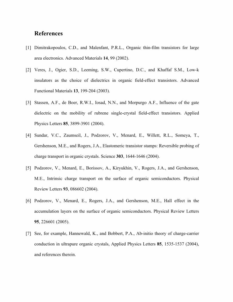
[1] Dimitrakopoulos, C.D., and Malenfant, P.R.L., Organic thin-film transistors for large
area electronics. Advanced Materials 14, 99 (2002).
[2] Veres, J., Ogier, S.D., Leeming, S.W., Cupertino, D.C., and Khaffaf S.M., Low-k
insulators as the choice of dielectrics in organic field-effect transistors. Advanced
Functional Materials 13, 199-204 (2003).
[3] Stassen, A.F., de Boer, R.W.I., Iosad, N.N., and Morpurgo A.F., Influence of the gate
dielectric on the mobility of rubrene single-crystal field-effect transistors. Applied
Physics Letters 85, 3899-3901 (2004).
[4] Sundar, V.C., Zaumseil, J., Podzorov, V., Menard, E., Willett, R.L., Someya, T.,
Gershenson, M.E., and Rogers, J.A., Elastomeric transistor stamps: Reversible probing of
charge transport in organic crystals. Science 303, 1644-1646 (2004).
[5] Podzorov, V., Menard, E., Borissov, A., Kiryukhin, V., Rogers, J.A., and Gershenson,
M.E., Intrinsic charge transport on the surface of organic semiconductors. Physical
Review Letters 93, 086602 (2004).
[6] Podzorov, V., Menard, E., Rogers, J.A., and Gershenson, M.E., Hall effect in the
accumulation layers on the surface of organic semiconductors. Physical Review Letters
95, 226601 (2005).
[7] See, for example, Hannewald, K., and Bobbert, P.A., Ab-initio theory of charge-carrier
conduction in ultrapure organic crystals, Applied Physics Letters 85, 1535-1537 (2004),
and references therein.
[8] Kirova, N., and Bussac, M.N., Self-trapping of electrons at the field-effect junction of a
molecular crystal, Physical Review B 68, 235312 (2003).
[9] de Boer, R.W.I., Gershenson, M.E., Morpurgo, A.F., and Podzorov, V., Organic single-
crystal field-effect transistors. Physica Status Solidi A 201, 1302-1331 (2004).
[10] Konofaos, N., Evangelou, E.K., Aslanoglou, X., Kokkoris, M., and Vlastou, R.,
Dielectric properties of CVD grown SiON thin films on Si for MOS microelectronic
devices. Semiconductor Science and Technology 19, 50-53 (2004).
[11] Meijer, E.J., Tanase, C., Blom, P.W.M., van Veenendaal, E., Huisman, B.H., de Leeuw
D.M., and Klapwijk, T.M., Switch-on voltage in disordered organic field-effect
transistors. Applied Physics Letters 80, 3838-3840 (2002).
[12] Chua, L.L., Zaumseil, J., Chang, J.F., Ou, E.C.W., Ho, P.K.H., Sirringhaus, H., and
Friend, R.H., General observation of n-type field-effect behaviour in organic
semiconductors. Nature 434, 194-199 (2005).
[13] Takeya, J., Tsukagoshi, K., Aoyagi, Y., Takenobu, T., and Iwasa, Y., Hall effect of quasi-
hole gas in organic single-crystal transistors. Japanese Journal of Applied Physics 44,
L1393-L1396 (2005).
[14] Austin, I.G. and Mott, N.F., Polarons in crystalline and non-crystalline materials.
Advances in Physics 50, 757 (1969).
[15] Emin, D. Semiclassical small-polaron hopping in a generalized molecular-crystal model
Phys. Rev. B 43, 11720-11724 (1991)
[16] Emin, D. Formation and hopping motion of molecular polarons. Phys. Rev. B 61, 14543-
14553 (2000)
[17] Mori, N. and Ando, T. Electron-optical-phonon interaction in single and double
heterostructures. Phys. Rev. B 40, 6175-6188 (1989)
[18] Bussac, M.N., Picon, J.D., and Zuppiroli L., The impact of molecular polarization on the
electronic properties of molecular semiconductors, Europhysics Letters 66, 392-398
(2004).
[19] da Silva Filho, D.A., Kim, E.-G., Brédas, J.-L. Transport properties in the rubrene crystal:
electronic coupling and vibrational reorganization energy. Advanced Materials 17, 1072-
1076 (2005)
[20] Houili, H. , Picon, J.D., Bussac, M.N., Zuppiroli, L. Polarization effects in the channel of
an organic field-effect transistor. Journal of Applied Physics 100, 023702 (2006)
[21] Feynman, R. P. and Hellwarth, R. W. and Iddings, C. K. and Platzman, P. M., Mobility
of Slow Electrons in a Polar Crystal, Phys. Rev. 127, 1004 (1962)
[22] Menard, E., Podzorov, V., Hur, S.H., Gaur, A., Gershenson, M.E., and Rogers, J.A.,
High-performance n- and p-type single-crystal organic transistors with free-space gate
dielectrics. Advanced Materials 16, 2097 (2004).
[23] Podzorov, V., Sysoev, S.E, Loginova, E., Pudalov, V.M., Gershenson, M.E., Single-
crystal organic field effect transistors with the hole mobility ~ 8 cm2/Vs. Applied
Physics Letters 83, 3504-3506 (2003).
[24] Podzorov, V., Pudalov, V.M., and Gershenson, M.E. Field-effect transistors on rubrene
single crystals with parylene gate insulator. Applied Physics Letters 82, 1739-1741
(2003).
[25] de Boer, R. W. I., Klapwijk, T. M., and Morpurgo A. F. Field-effect transistors on
tetracene single crystals. Applied Physics Letters 84, 296 (2004).
Captions
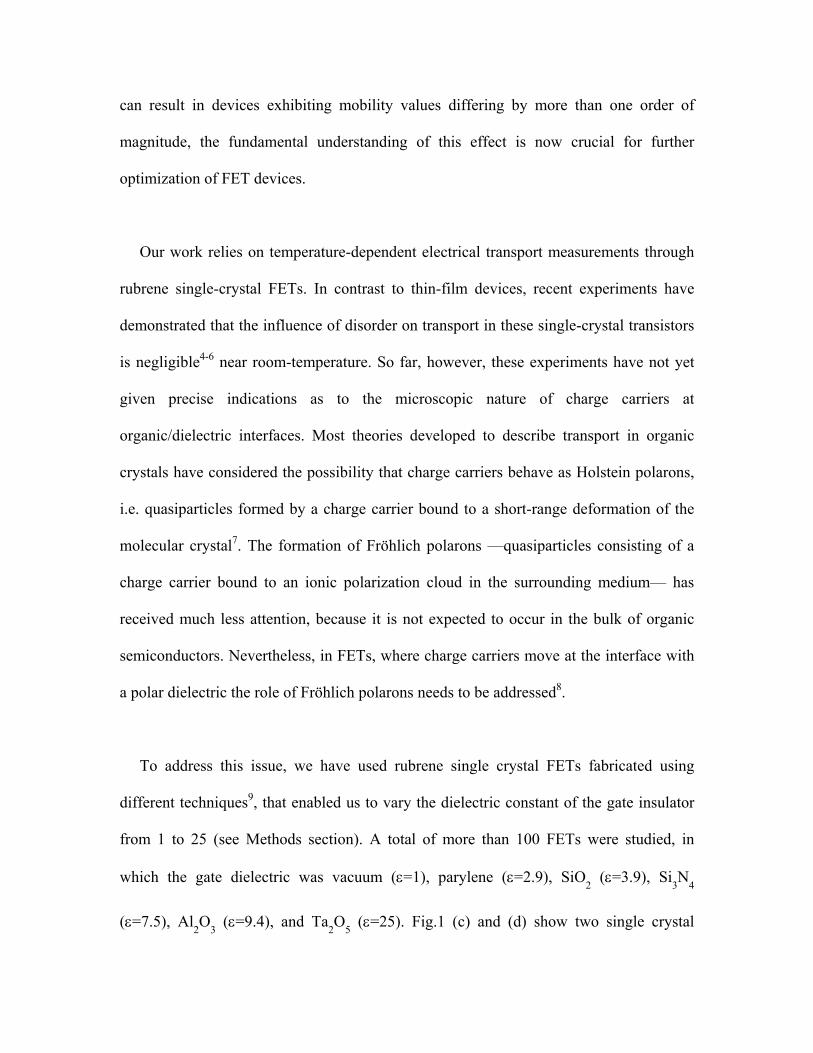
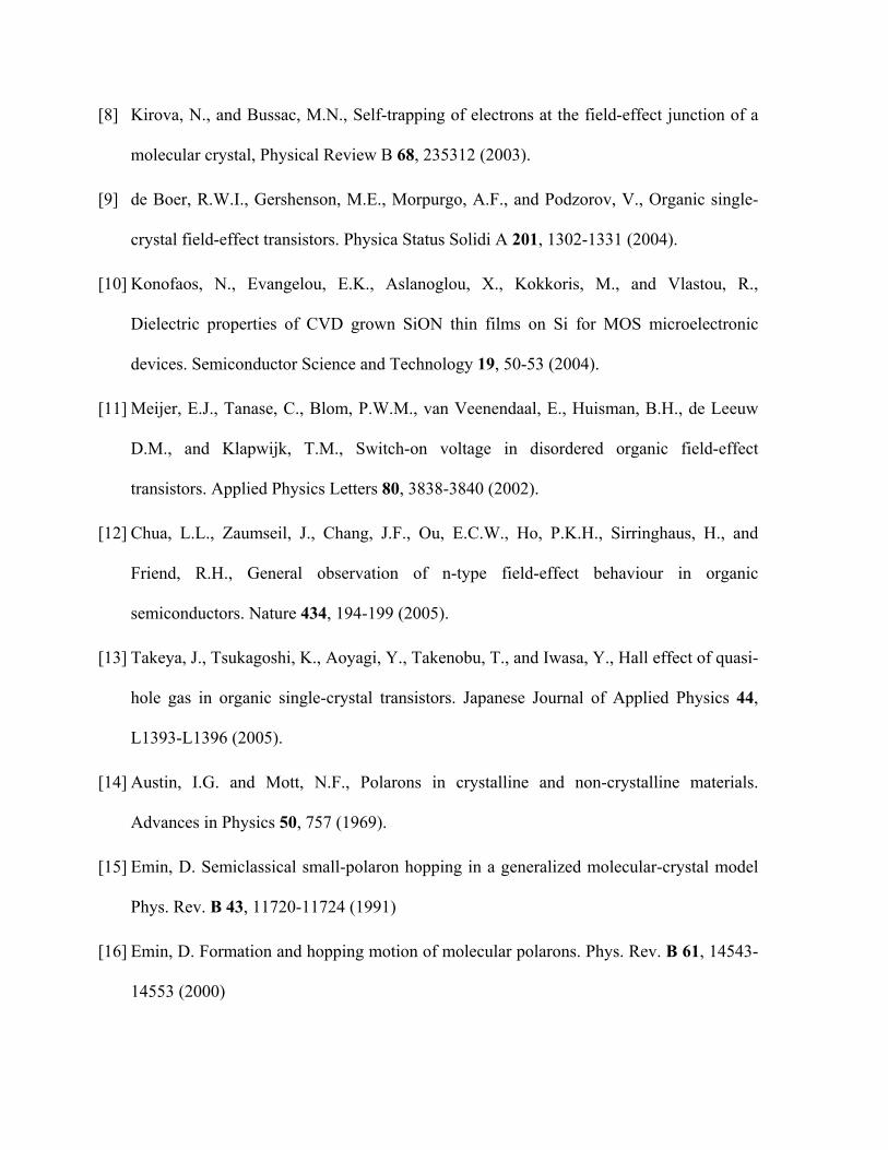
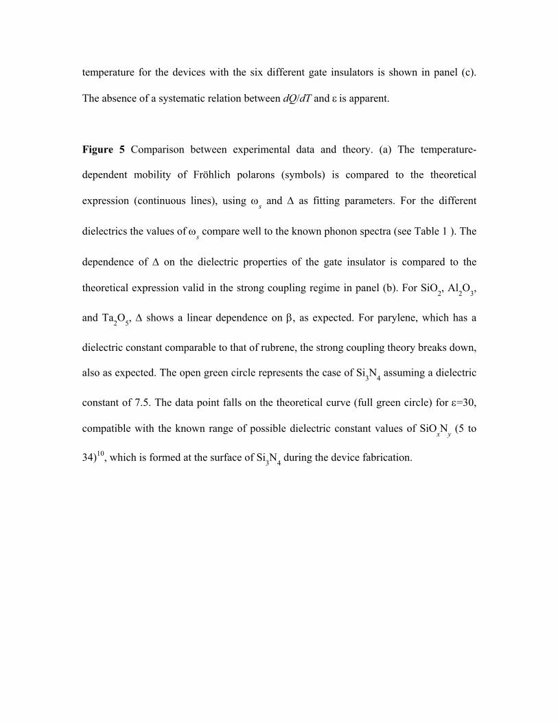
Figure 1 High-quality organic single-crystal transistors. (a) Schematic representation
of the single-crystal FETs used in our investigation. Electrostatically induced holes
moving at the dielectric/organic interface polarize the gate dielectric as illustrated in (b).
For sufficiently large coupling (i.e., dielectric constant) the hole and the induced charge
can move together, resulting in the formation of a Fröhlich polaron. Panels (c) and (d) are
optical microscope images of actual devices (the color is determined by the microscope
settings). Typical examples of the device current versus gate voltage measured at
different temperatures (1, T= 295 K; 2, T= 270 K; 3, T= 250 K; 4, T= 230 K; 5, T= 210
K) are shown in panel (e) and (f) for devices with vacuum (VSD
=5 V) and Al2O
3 (V
SD=1
V) as gate dielectric, respectively.
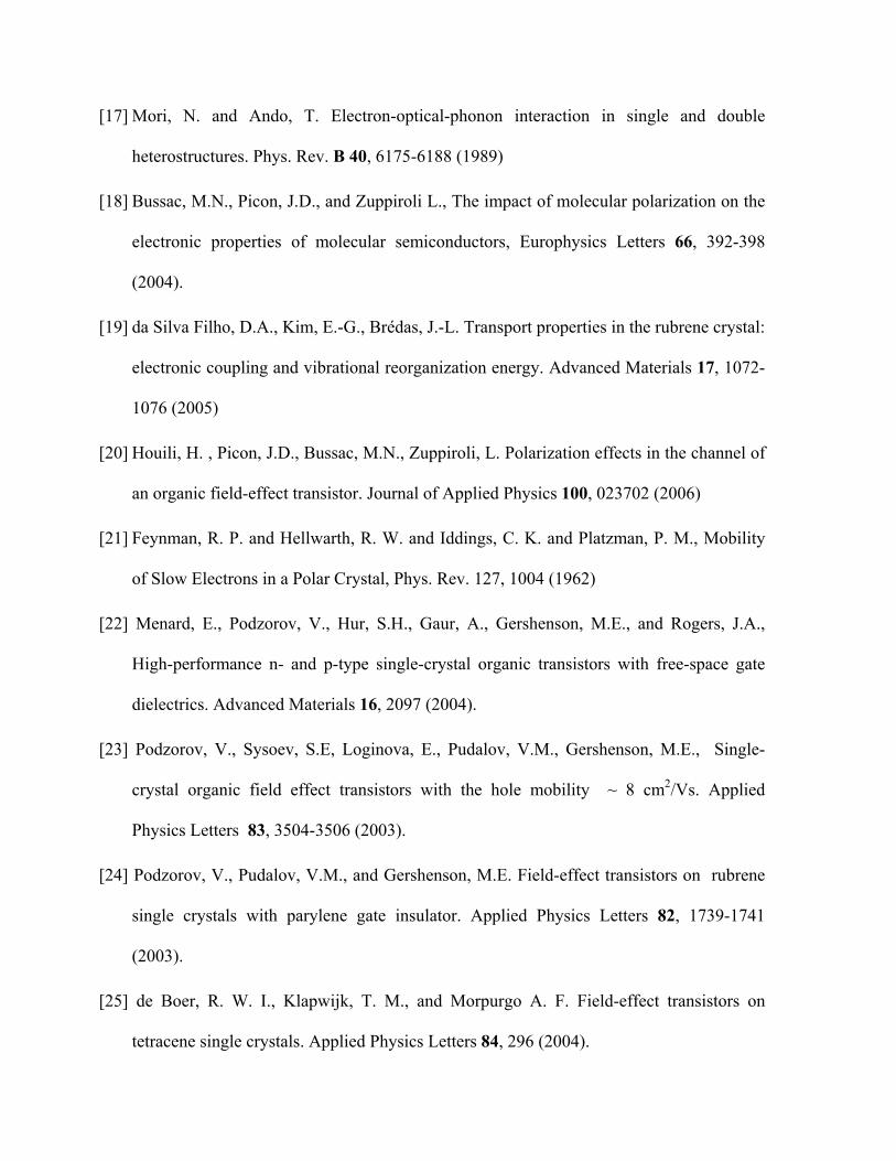
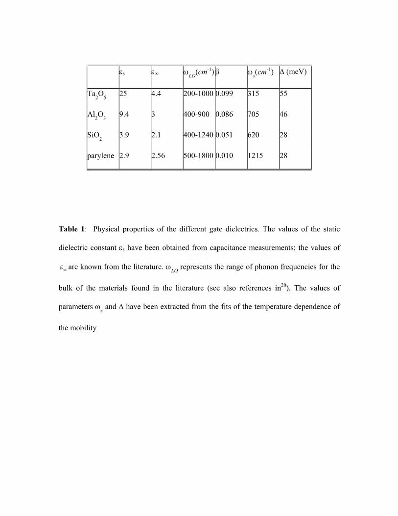
Figure 2 Gate voltage dependence of the carrier mobility. The panels show the
mobility of devices fabricated on different gate dielectrics, extracted from measurements
of the source-drain current in the linear regime. In all cases, the mobility is essentially
independent on gate voltage, which enables an easy comparison of different devices. In
all panels 1 corresponds to T= 295 K, 2 to T= 270 K, 3 to T= 250 K, 4 to T= 230 K, 5 to
T= 200 K, 6 to T= 175 K, 7 to T= 150 K. For devices with SiO2 as gate insulator, the
mobility is essentially temperature independent in the range investigated, for all values of
gate voltage.
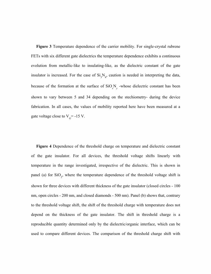
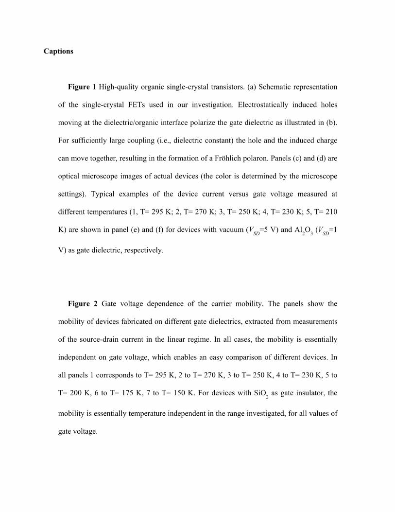
Figure 3 Temperature dependence of the carrier mobility. For single-crystal rubrene
FETs with six different gate dielectrics the temperature dependence exhibits a continuous
evolution from metallic-like to insulating-like, as the dielectric constant of the gate
insulator is increased. For the case of Si3N
4, caution is needed in interpreting the data,
because of the formation at the surface of SiOxN
y -whose dielectric constant has been
shown to vary between 5 and 34 depending on the stechiometry- during the device
fabrication. In all cases, the values of mobility reported here have been measured at a
gate voltage close to VG= -15 V.
Figure 4 Dependence of the threshold charge on temperature and dielectric constant
of the gate insulator. For all devices, the threshold voltage shifts linearly with
temperature in the range investigated, irrespective of the dielectric. This is shown in
panel (a) for SiO2, where the temperature dependence of the threshold voltage shift is
shown for three devices with different thickness of the gate insulator (closed circles - 100
nm, open circles - 200 nm, and closed diamonds - 500 nm). Panel (b) shows that, contrary
to the threshold voltage shift, the shift of the threshold charge with temperature does not
depend on the thickness of the gate insulator. The shift in threshold charge is a
reproducible quantity determined only by the dielectric/organic interface, which can be
used to compare different devices. The comparison of the threshold charge shift with
temperature for the devices with the six different gate insulators is shown in panel (c).
The absence of a systematic relation between dQ/dT and g is apparent.
Figure 5 Comparison between experimental data and theory. (a) The temperature-
dependent mobility of Fröhlich polarons (symbols) is compared to the theoretical
expression (continuous lines), using ys and F as fitting parameters. For the different
dielectrics the values of ys compare well to the known phonon spectra (see Table 1 ). The
dependence of F on the dielectric properties of the gate insulator is compared to the
theoretical expression valid in the strong coupling regime in panel (b). For SiO2, Al
2O
3,
and Ta2O
5, F shows a linear dependence on d, as expected. For parylene, which has a
dielectric constant comparable to that of rubrene, the strong coupling theory breaks down,
also as expected. The open green circle represents the case of Si3N
4 assuming a dielectric
constant of 7.5. The data point falls on the theoretical curve (full green circle) for g=30,
compatible with the known range of possible dielectric constant values of SiOxN
y (5 to
34)10, which is formed at the surface of Si3N
4 during the device fabrication.
gs gı yLO
(cm-1) d ys(cm-1) F (meV)
Ta2O
5 25 4.4 200-1000 0.099 315 55
Al2O
3 9.4 3 400-900 0.086 705 46
SiO2 3.9 2.1 400-1240 0.051 620 28
parylene 2.9 2.56 500-1800 0.010 1215 28
Table 1: Physical properties of the different gate dielectrics. The values of the static
dielectric constant gs have been obtained from capacitance measurements; the values of
g¢ are known from the literature. yLO
represents the range of phonon frequencies for the
bulk of the materials found in the literature (see also references in20). The values of
parameters ys and F have been extracted from the fits of the temperature dependence of
the mobility
Single crystalMetallic contacts
dielectricSi
300 µm
1 mm
- - - - -
++++
(a)
(c)
(b)
(d)
(f )(e)
Figure 1, Hulea et al.
1
-20 -15 -10 -5
1
2
3
4
5
-25 -20 -15 -10 -51
2
3
4
5-20 -15 -10
4
6
8
10
-30 -25 -20 -15 -10 -50
1
2
3
(b)
VG (V)
Al2O3
1 3 5 2 4
(cm
2 /Vs)
(d)
Si3N4
1 3 5 2 4
(a)
1 5
SiO2
(c)
Ta2O5
1 4 6 2 5 7
Figure 2, Hulea et al.
1
150 200 250 300
1
10
Ta2O
5
Si3N
4
Al2O
3
SiO2
Parylene
Vacuum
(cm
2 /Vs)
T (K)
Figure 3, Hulea et al.
1
0 5 10 15 20 250.0
1.0
2.0
3.0
4.00 500
0.5
1.0
1.5
200 250 300-20
-10
0
(c)
dQ/d
T (1
010 h
/K c
m2 )
d (nm)
(b)(a)
V TH (V
)
dQ/d
T (1
010 h
/Kcm
2 )
T (K)
Figure 4, Hulea et al.
1
150 200 250 3000.1
1
10
0.05 0.100
20
40
60
parylene SiO
2 Al
2O
3 Si
3N
4 Ta
2O
5
P(cm
2 /Vs)
T (K)0
(m
eV)
Figure 5, Hulea et al.
1