TSC2000 Datasheet PDF - Texas Instruments · PRODUCTION DATA information is current as of...
38
www.ti.com PRODUCTION DATA information is current as of publication date. Products conform to specifications per the terms of Texas Instruments standard warranty. Production processing does not necessarily include testing of all parameters. Copyright © 2002, Texas Instruments Incorporated Please be aware that an important notice concerning availability, standard warranty, and use in critical applications of Texas Instruments semiconductor products and disclaimers thereto appears at the end of this data sheet. FEATURES ● 4-WIRE TOUCH SCREEN INTERFACE ● RATIOMETRIC CONVERSION ● SINGLE 2.7V TO 3.6V SUPPLY ● SERIAL INTERFACE ● INTERNAL DETECTION OF SCREEN TOUCH ● PROGRAMMABLE 8-, 10-, OR 12-BIT RESOLUTION ● PROGRAMMABLE SAMPLING RATES ● DIRECT BATTERY MEASUREMENT (0.5V to 6V) ● ON-CHIP TEMPERATURE MEASUREMENT ● TOUCH-PRESSURE MEASUREMENT ● FULL POWER-DOWN CONTROL ● TSSOP-20 PACKAGE APPLICATIONS ● PERSONAL DIGITAL ASSISTANTS ● CELLULAR PHONES ● MP3 PLAYERS PDA ANALOG INTERFACE CIRCUIT DESCRIPTION The TSC2000 is a complete PDA analog interface circuit. It contains a complete 12-bit, Analog-to-Digital (A/D) resistive touch screen converter including drivers, the control to mea- sure touch pressure, and an 8-bit Digital-to-Analog (D/A) converter output for LCD contrast control. The TSC2000 interfaces to the host controller through a standard SPI™ serial interface. The TSC2000 offers programmable resolution and sampling rates from 8- to 12-bits and up to 125kHz to accommodate different screen sizes. The TSC2000 also offers two battery-measurement inputs, one of which is capable of reading battery voltages up to 6V while operating at only 2.7V. It also has an on-chip temperature sensor capable of reading 0.3°C resolution. The TSC2000 is available in a TSSOP-20 package. TSC2000 SBAS257 – FEBRUARY 2002 SPI is a registered trademark of Motorola. US Patent No. 624639. A/D Converter Internal 2.5V Reference MUX Serial Interface and Control Logic D/A Converter MISO SS SCLK MOSI DAV PENIRQ Touch Panel Drivers Temp Sensor Battery Monitor Battery Monitor X+ X– Y+ Y– V BAT1 V BAT2 Clock AUX1 AUX2 V REF ARNG A OUT ® TSC2000
Transcript of TSC2000 Datasheet PDF - Texas Instruments · PRODUCTION DATA information is current as of...

www.ti.com
PRODUCTION DATA information is current as of publication date.Products conform to specifications per the terms of Texas Instrumentsstandard warranty. Production processing does not necessarily includetesting of all parameters.
Copyright © 2002, Texas Instruments Incorporated
Please be aware that an important notice concerning availability, standard warranty, and use in critical applications ofTexas Instruments semiconductor products and disclaimers thereto appears at the end of this data sheet.
FEATURES 4-WIRE TOUCH SCREEN INTERFACE
RATIOMETRIC CONVERSION
SINGLE 2.7V TO 3.6V SUPPLY
SERIAL INTERFACE
INTERNAL DETECTION OF SCREEN TOUCH
PROGRAMMABLE 8-, 10-, OR 12-BITRESOLUTION
PROGRAMMABLE SAMPLING RATES
DIRECT BATTERY MEASUREMENT (0.5V to 6V)
ON-CHIP TEMPERATURE MEASUREMENT
TOUCH-PRESSURE MEASUREMENT
FULL POWER-DOWN CONTROL
TSSOP-20 PACKAGE
APPLICATIONS PERSONAL DIGITAL ASSISTANTS
CELLULAR PHONES
MP3 PLAYERS
PDA ANALOG INTERFACE CIRCUIT
DESCRIPTIONThe TSC2000 is a complete PDA analog interface circuit. Itcontains a complete 12-bit, Analog-to-Digital (A/D) resistivetouch screen converter including drivers, the control to mea-sure touch pressure, and an 8-bit Digital-to-Analog (D/A)converter output for LCD contrast control. The TSC2000interfaces to the host controller through a standard SPI™serial interface. The TSC2000 offers programmable resolutionand sampling rates from 8- to 12-bits and up to 125kHz toaccommodate different screen sizes.
The TSC2000 also offers two battery-measurement inputs,one of which is capable of reading battery voltages up to 6Vwhile operating at only 2.7V. It also has an on-chip temperaturesensor capable of reading 0.3°C resolution. The TSC2000 isavailable in a TSSOP-20 package.
TSC2000
SBAS257 – FEBRUARY 2002
SPI is a registered trademark of Motorola.
US Patent No. 624639.
A/D Converter
Internal 2.5VReference
MUX
SerialInterface
andControlLogic
D/A Converter
MISO
SS
SCLK
MOSI
DAV
PENIRQ
Touch PanelDrivers
Temp Sensor
Battery Monitor
Battery Monitor
X+X–Y+Y–
VBAT1
VBAT2
Clock
AUX1
AUX2
VREF
ARNG
AOUT
®TSC2000

2www.ti.com
TSC2000SBAS257
ABSOLUTE MAXIMUM RATINGS(1)
VDD to GND ........................................................................... –0.3V to +6VDigital Input Voltage to GND ................................... –0.3V to VDD + 0.3VOperating Temperature Range ...................................... –40°C to +105°CStorage Temperature Range ......................................... –65°C to +150°CJunction Temperature (TJ Max) .................................................... +150°CTSSOP Package
Power Dissipation .................................................... (TJ Max – TA)/θJA
θJA Thermal Impedance .......................................................... 93°C/WLead Temperature, Soldering
Vapor Phase (60s) ............................................................ +215°CInfrared (15s) ..................................................................... +220°C
NOTE: (1) Stresses above those listed under “Absolute Maximum Ratings”may cause permanent damage to the device. Exposure to absolute maximumconditions for extended periods may affect device reliability.
INTEGRAL SPECIFIEDLINEARITY PACKAGE TEMPERATURE PACKAGE ORDERING TRANSPORT
PRODUCT ERROR (LSB) PACKAGE-LEAD DESIGNATOR(1) RANGE MARKING NUMBER(2) MEDIA, QUANTITY
TSC2000IPW ±2 TSSOP-20 PW –40°C to +85°C TSC2000I TSC2000IPW Rails, 70
" " " " " " TSC2000IPWR Tape and Reel, 2000
NOTES: (1) For the most current specifications and package information, refer to our web site at www.ti.com. (2) Models labeled with “R” indicates large quantitytape and reel.
PIN CONFIGURATION
Top View TSSOP
PIN DESCRIPTIONPIN NAME DESCRIPTION
1 VDD Power Supply
2 X+ X+ Position Input
3 Y+ Y+ Position Input
4 X– X– Position Input
5 Y– Y– Position Input
6 GND Ground
7 VBAT1 Battery Monitor Input 1
8 VBAT2 Battery Monitor Input 2
9 VREF Voltage Reference Input/Output
10 NC No Connection
11 SCLK Serial Clock Input
12 SS Slave Select Input (Active LOW). Data will not beclocked in to MOSI unless SS is LOW. When SS isHIGH, MISO is high impedance.
13 MOSI Serial Data Input. Data is clocked in at SCLK fallingedge.
14 DAV Data Available (Active LOW)
15 MISO Serial Data Output. Data is clocked out at SCLKfalling edge. High impedance when SS is HIGH.
16 PENIRQ Pen Interrupt
17 AOUT Analog Output Current from D/A Converter
18 ARNG D/A Converter Analog Output Range Set
19 AUX2 Auxiliary A/D Converter Input 2
20 AUX1 Auxiliary A/D Converter Input 1
ELECTROSTATICDISCHARGE SENSITIVITY
This integrated circuit can be damaged by ESD. TexasInstruments recommends that all integrated circuits be handledwith appropriate precautions. Failure to observe proper han-dling and installation procedures can cause damage.
ESD damage can range from subtle performance degrada-tion to complete device failure. Precision integrated circuitsmay be more susceptible to damage because very smallparametric changes could cause the device not to meet itspublished specifications.
+VDD
X+
Y+
X–
Y–
GND
VBAT1
VBAT2
VREF
NC
AUX1
AUX2
ARNG
AOUT
PENIRQ
MISO
DAV
MOSI
SS
SCLK
1
2
3
4
5
6
7
8
9
10
20
19
18
17
16
15
14
13
12
11
TSC2000

3www.ti.com
TSC2000SBAS257
PARAMETER CONDITIONS MIN TYP MAX UNITS
AUXILIARY ANALOG INPUTInput Voltage Range 0 +VREF VInput Capacitance 25 pFInput Leakage Current ±1 µA
BATTERY MONITOR INPUTInput Voltage Range VBAT1 0.5 6.0 VInput Voltage Range VBAT2 0.5 3.0 VInput Capacitance 25 pFInput Leakage Current ±1 µAAccuracy –3 +3 %
TEMPERATURE MEASUREMENTTemperature Range –40 +85 °CTemperature Resolution 0.3 °CAccuracy ±2 °C
A/D CONVERTERResolution Programmable: 8-, 10-, or 12-Bits 12 BitsNo Missing Codes 12-Bit Resolution 11 BitsIntegral Linearity ±2 LSBOffset Error ±6 LSBGain Error Excluding Reference Error ±6 LSBNoise 30 µVrmsPower-Supply Rejection 80 dB
D/A CONVERTEROutput Current Range Set by Resistor from ARNG to GND 650 µAResolution 8 BitsIntegral Linearity ±2 LSB
VOLTAGE REFERENCEVoltage Range Internal 2.5V 2.45 2.5 2.55 V
Internal 1.25V 1.225 1.25 1.275 VReference Drift 20 ppm/°CExternal Reference Input Range 1.0 VDD VCurrent Drain External Reference 20 µA
DIGITAL INPUT/OUTPUTInternal Clock Frequency 8 MHzLogic Family CMOSLogic Levels: VIH IIH = +5µA 0.7VDD V
VIL IIL = +5µA –0.3 0.3VDD VVOH IOH = 2 TTL Loads 0.8VDD VVOL IOL = 2 TTL Loads 0.4 V
POWER-SUPPLY REQUIREMENTSPower-Supply Voltage, +VDD Specified Performance 2.7 3.6 VQuiescent Current See Note (1) 1.25 2.3 mA
See Note (2) 500 µAPower Down 3 µA
TEMPERATURE RANGESpecified Performance –40 +85 °C
NOTES: (1) AUX1 conversion, no averaging, no REF power down, 50µs conversion. (2) AUX1 conversion, no averaging, external reference, 50µs conversion.
ELECTRICAL CHARACTERISTICSAt –40°C to +85°C, +VDD = +2.7V, internal VREF = +2.5V, conversion clock = 2MHz, 12-bit mode, unless otherwise noted.
TSC2000IPW

4www.ti.com
TSC2000SBAS257
TIMING DIAGRAMAll specifications typical at –40°C to +85°C, +VDD = +2.7V.
ttd
tLag
tdis
tLead
tsck
twsck
twsck
thitsu
tho
ta
tv
trtf
SS
SCLK
MSB OUT
MSB IN LSB IN
LSB OUTBIT 6 ... 1
BIT 6 ... 1
MISO
MOSI
PARAMETER CONDITIONS MIN TYP MAX UNITS
SCLK Period tsck 30 nsEnable Lead Time tLead 15 nsEnable Lag Time tLag 15 nsSequential Transfer Delay ttd 30 nsData Setup Time tsu 10 nsData Hold Time (inputs) thi 10 nsData Hold Time (outputs) tho 0 nsSlave Access Time ta 15 nsSlave DOUT Disable Time tdis 15 nsDataValid tv 10 nsRise Time tr 30 nsFall Time tf 30 ns
TIMING CHARACTERISTICS(1)(2)
At –40°C to +85°C, +VDD = +2.7V, VREF = +2.5V, unless otherwise noted.
TSC2000
NOTES: (1) All input signals are specified with tr = tf = 5ns (10% to 90% of VDD) and timed from a voltage level of (VIL + VIH)/2. (2) See timing diagram below.

5www.ti.com
TSC2000SBAS257
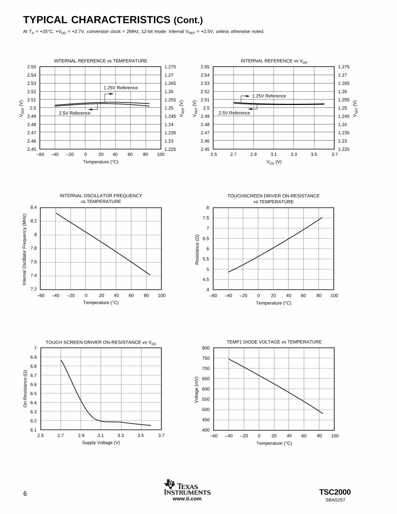
TYPICAL CHARACTERISTICSAt TA = +25°C, +VDD = +2.7V, conversion clock = 2MHz, 12-bit mode. Internal VREF = +2.5V, unless otherwise noted.
CONVERSION SUPPLY CURRENT vs TEMPERATURE(AUX1 Conversion, No Averaging,
No REF Power-Down, 20µs Conversion)
0–60 100–40 –20 20
Temperature (°C)
I DD (
mA
)
2
1.95
1.9
1.85
1.8
1.7540 60 80
POWER-DOWN SUPPLY CURRENT vs TEMPERATURE
0–60 100–40 –20 20
Temperature (°C)
I DD (
nA)
7
6
5
4
3
2
1
040 60 80
POWER-DOWN SUPPLY CURRENT vs SUPPLY VOLTAGE
2.92.5 3.73.1
Supply Voltage (V)
Pow
er-D
own
Cur
rent
(nA
)
0.12
0.11
0.1
0.09
0.08
0.07
0.063.3 3.52.7
INTERNAL OSCILLATOR FREQUENCY vs VDD
3.12.5 3.72.7 3.3
VDD (V)
Inte
rnal
Osc
illat
or F
requ
ency
(M
Hz)
8.3
8.25
8.2
8.15
8.1
8.05
8
7.95
7.9
7.85
7.83.52.9
CHANGE IN GAIN ERROR vs TEMPERATURE
0–60 100–40 –20 20
Temperature (°C)
Cha
nge
in G
ain
Err
or (
LSB
)
0.5
0.4
0.3
0.2
0.1
0
–0.1
–0.2
–0.3
–0.4
–0.5
40 60 80
CHANGE IN OFFSET ERROR vs TEMPERATURE
0–60 100–40 –20 20
Temperature (°C)
Cha
nge
in O
ffset
(LS
B)
40 60 80
0.5
0.4
0.3
0.2
0.1
0
–0.1
–0.2
–0.3
–0.4
–0.5
6www.ti.com
TSC2000SBAS257
TYPICAL CHARACTERISTICS (Cont.)At TA = +25°C, +VDD = +2.7V, conversion clock = 2MHz, 12-bit mode. Internal VREF = +2.5V, unless otherwise noted.
INTERNAL REFERENCE vs TEMPERATURE
20 40–60 100–40 –20 0 60 80
Temperature (°C)
VR
EF (
V)
2.55
2.54
2.53
2.52
2.51
2.5
2.49
2.48
2.47
2.46
2.45
VR
EF (
V)
1.275
1.27
1.265
1.26
1.255
1.25
1.245
1.24
1.235
1.23
1.225
2.5V Reference
1.25V Reference
INTERNAL REFERENCE vs VDD
3.3 3.52.5 3.72.7 2.9 3.1
VDD (V)
VR
EF (
V)
2.55
2.54
2.53
2.52
2.51
2.5
2.49
2.48
2.47
2.46
2.45
VR
EF (
V)
1.275
1.27
1.265
1.26
1.255
1.25
1.245
1.24
1.235
1.23
1.225
2.5V Reference
1.25V Reference
INTERNAL OSCILLATOR FREQUENCYvs TEMPERATURE
0–60 100–40 –20 20
Temperature (°C)
Inte
rnal
Osc
illat
or F
requ
ency
(M
Hz)
8.4
8.2
8
7.8
7.6
7.4
7.240 60 80
TOUCHSCREEN DRIVER ON-RESISTANCEvs TEMPERATURE
0–60 100–40 –20 20
Temperature (°C)
Res
ista
nce
(Ω)
8
7.5
7
6.5
6
5.5
5
4.5
440 60 80
TOUCH SCREEN DRIVER ON-RESISTANCE vs VDD
3.12.5 3.72.7 3.3
Supply Voltage (V)
On-
Res
ista
nce
(Ω)
7
6.9
6.8
6.7
6.6
6.5
6.4
6.3
6.2
6.13.52.9
TEMP1 DIODE VOLTAGE vs TEMPERATURE
0–60 100–40 –20 20
Temperature (°C)
Vol
tage
(m
V)
800
750
700
650
600
550
500
450
40040 60 80

7www.ti.com
TSC2000SBAS257
TYPICAL CHARACTERISTICS (Cont.)At TA = +25°C, +VDD = +2.7V, conversion clock = 2MHz, 12-bit mode. Internal VREF = +2.5V, unless otherwise noted.
900
800
700
600
500
Vol
tage
(m
V)
Temperature (°C)
–60 –40 –20 0 20 40 60 80 100
TEMP2 DIODE VOLTAGE vs TEMPERATURE TEMP1 DIODE VOLTAGE vs VDD
3.12.5 3.72.7 3.3
VDD (V)
TE
MP
1 V
olta
ge (m
V)
612.0
611.8
611.6
611.4
611.2
611.0
610.8
610.6
610.4
610.2
610.03.52.9
TEMP2 DIODE VOLTAGE vs VDD
3.12.5 3.72.7 3.3
VDD (V)
Tem
p2 V
olta
ge (m
V)
740
738
736
734
732
730
728
726
724
722
7203.52.9
DAC OUTPUT CURRENT vs TEMPERATURE
0–60 100–40 –20 20
Temperature (°C)
DA
C O
utpu
t Cur
rent
(m
A)
1
0.95
0.9
0.85
0.8
0.75
0.7
0.65
0.640 60 80
DAC MAX CURRENT vs VDD
3.12.5 3.72.7 3.3
VDD (V)
DA
C O
utpu
t Cur
rent
(mA
)
0.91
0.905
0.9
0.895
0.89
0.885
0.88
0.8753.52.9

8www.ti.com
TSC2000SBAS257
FIGURE 1. Typical Circuit Configuration.
OVERVIEWThe TSC2000 is an analog interface circuit for human inter-face devices. A register-based architecture eases integrationwith microprocessor-based systems through a standard SPIbus. All peripheral functions are controlled through the reg-isters and onboard state machines.
The TSC2000 consists of the following blocks (refer to theblock diagram on the front page):
• Touch Screen Interface
• Battery Monitors
• Auxiliary Inputs
• Temperature Monitor
• Current Output D/A Converter
Communication to the TSC2000 is via a standard SPI serialinterface. This interface requires that the Slave Select signal bedriven LOW to communicate with the TSC2000. Data is thenshifted into or out of the TSC2000 under control of the hostmicroprocessor, which also provides the serial data clock.
Control of the TSC2000 and its functions is accomplished bywriting to different registers in the TSC2000. A simple com-mand protocol is used to address the 16-bit registers. Reg-isters control the operation of the A/D converter and D/Aconverter.
The result of measurements made will be placed in theTSC2000’s memory map and may be read by the host at anytime. Three signals are available from the TSC2000 to indicatethat data is available for the host to read. The DAV outputindicates that an A/D conversion has completed and that datais available. The PENIRQ output indicates that a touch hasbeen detected on the touch screen. A typical application of theTSC2000 is shown in Figure 1.
+
Auxiliary Input
Auxiliary Input
Pen Interrupt Request
Serial Data Out
Data Available
Serial Data In
Slave Select
Serial Clock
1µF to
10µF(Optional)
+2.7V to +3.3V
Touch Screen
0.1µF
+VDD
X+
Y+
X–
Y–
GND
VBAT1
VBAT2
VREF
NC
AUX1
AUX2
ARNG
AOUT
PENIRQ
MISO
DAV
MOSI
SS
SCLK
1
2
3
4
5
6
7
8
9
10
20
19
18
17
16
15
14
13
12
11
TSC2000
+1µF to
10µF(Optional)
0.1µF
MainBattery
SecondaryBattery
LCD Contrast
VoltageRegulator
RRNG

9www.ti.com
TSC2000SBAS257
FIGURE 2. 4-Wire Touch Screen Construction.
FIGURE 3. Pressure Measurement.
OPERATION—TOUCH SCREEN
A resistive touch screen works by applying a voltage acrossa resistor network and measuring the change in resistance ata given point on the matrix where a screen is touched by aninput stylus, pen, or finger. The change in the resistance ratiomarks the location on the touch screen.
The TSC2000 supports the resistive 4-wire configurations(see Figure 1). The circuit determines location in two coordi-nate pair dimensions, although a third dimension can beadded for measuring pressure.
THE 4-WIRE TOUCH SCREEN COORDINATEPAIR MEASUREMENT
A 4-wire touch screen is constructed as shown in Figure 2.It consists of two transparent resistive layers separated byinsulating spacers.
The 4-wire touch screen panel works by applying a voltageacross the vertical or horizontal resistive network. The A/Dconverter converts the voltage measured at the point thepanel is touched. A measurement of the Y-position of thepointing device is made by connecting the X+ input to a dataconverter chip, turning on the Y+ and Y– drivers, anddigitizing the voltage seen at the X+ input. The voltagemeasured is determined by the voltage divider developed atthe point of touch. For this measurement, the horizontalpanel resistance in the X+ lead does not affect the conver-sion due to the high input impedance of the A/D converter.
Voltage is then applied to the other axis, and the A/Dconverter converts the voltage representing the X-position onthe screen. This provides the X- and Y-coordinates to theassociated processor.
Measuring touch pressure (Z) can also be done with theTSC2000. To determine pen or finger touch, the pressure ofthe “touch” needs to be determined. Generally, it is notnecessary to have very high performance for this test, there-
fore, the 8-bit resolution mode is recommended (however,calculations will be shown with the 12-bit resolution mode).There are several different ways of performing this measure-ment. The TSC2000 supports two methods. The first methodrequires knowing the X-plate resistance, measurement of theX-position, and two additional cross panel measurements (Z2
and Z1) of the touch screen, as seen in Figure 3. UsingEquation 1 will calculate the touch resistance:
R RX-Position
4096ZZ
–1TOUCH X-Plate2
1=
• (1)
The second method requires knowing both the X-plate andY-plate resistance, measurement of X-position and Y-posi-tion, and Z1. Using Equation 2 will also calculate the touchresistance: (2)
R RX-Position
40964096
Z–1 R
Y-Position4096TOUCH X-Plate
1-Plate=
−• •Y
When the touch panel is pressed or touched, and the driversto the panel are turned on, the voltage across the touch panelwill often overshoot and then slowly settle (decay) down to astable DC value. This is due to mechanical bouncing whichis caused by vibration of the top layer sheet of the touchpanel when the panel is pressed. This settling time must beaccounted for, or else the converted value will be in error.Therefore, a delay must be introduced between the time thedriver for a particular measurement is turned on, and the timemeasurement is made.
Conductive Bar
InsulatingMaterial(Glass)
SilverInk
Transparent Conductor (ITO)Bottom Side
Transparent Conductor (ITO)Top Side
X+
X–
Y+
Y–
ITO = Indium Tin Oxide
X-Position
Measure X-Position
Measure Z1-Position
Touch
X+ Y+
X– Y–
Z1-Position
Touch
X+ Y+
Y–X–
Measure Z2-Position
Z2-Position
Touch
X+ Y+
Y–X–

10www.ti.com
TSC2000SBAS257
FIGURE 4. Simplified Diagram of the Analog Input Section.
In some applications, external capacitors may be requiredacross the touch screen for filtering noise picked up by thetouch screen; i.e., noise generated by the LCD panel orback-light circuitry. The value of these capacitors will providea low-pass filter to reduce the noise, but will cause anadditional settling time requirement when the panel is touched.
Several solutions to this problem are available in the TSC2000.A programmable delay time is available which sets the delaybetween turning the drivers on and making a conversion.This is referred to as the Panel Voltage Stabilization time,and is used in some of the modes available in the TSC2000.In other modes, the TSC2000 can be commanded to turn onthe drivers only without performing a conversion. Time canthen be allowed before a conversion is started.
The TSC2000 touch screen interface can measure position (Xand Y) and pressure (Z). Determination of these coordinatesis possible under three different modes of the A/D converter:conversion controlled by the TSC2000, initiated by detection ofa touch; conversion controlled by the TSC2000, initiated by thehost responding to the PENIRQ signal; or conversion com-pletely controlled by the host processor.
A/D CONVERTER
The analog inputs of the TSC2000 are shown in Figure 4. Theanalog inputs (X, Y, and Z touch panel coordinates, batteryvoltage monitors, chip temperature, and auxiliary inputs) areprovided via a multiplexer to the Successive ApproximationRegister (SAR) A/D converter. The A/D converter architectureis based on capacitive redistribution architecture which inher-ently includes a sample-and-hold function.
Converter
–REF
+REF+IN
–IN
VBAT1
AUX1
BatteryOn
AUX2
GND
2.5VReference
Ref ON/OFF
X+
X–
+VDD
TEMP1
Y+
Y–
VREF
TEMP0
7.5kΩ
VBAT2
2.5kΩ
2.5kΩ
BatteryOn
2.5kΩ

11www.ti.com
TSC2000SBAS257
FIGURE 5. Ideal Input Voltages and Output Codes.
FIGURE 6. PENIRQ Functional Block Diagram.
A unique configuration of low on-resistance switches allowsan unselected A/D converter input channel to provide powerand an accompanying pin to provide ground for driving thetouch panel. By maintaining a differential input to the con-verter and a differential reference input architecture, it ispossible to negate errors caused by the driver switch on-resistances.
The A/D converter is controlled by an A/D Converter ControlRegister. Several modes of operation are possible, depend-ing upon the bits set in the control register. Channel selec-tion, scan operation, averaging, resolution, and conversionrate may all be programmed through this register. Thesemodes are outlined in the sections below for each type ofanalog input. The results of conversions made are stored inthe appropriate result register.
Data Format
The TSC2000 output data is in Straight Binary format, asshown in Figure 5. This figure shows the ideal output code forthe given input voltage and does not include the effects ofoffset, gain, or noise.
Reference
The TSC2000 has an internal voltage reference that can beset to 1.25V or 2.5V, through the Reference Control Register.
The internal reference voltage is only used in the single-ended mode for battery monitoring, temperature measure-ment, and for utilizing the auxiliary inputs. Optimal touchscreen performance is achieved when using a ratiometricconversion, thus all touch screen measurements are doneautomatically in the differential mode. An external referencecan also be applied to the VREF pin, and the internal refer-ence can be turned off.
Variable Resolution
The TSC2000 provides three different resolutions for the A/Dconverter: 8-, 10-, or 12-bits. Lower resolutions are oftenpractical for measurements such as touch pressure. Perform-
ing the conversions at lower resolutions reduces the amount oftime it takes for the A/D converter to complete its conversionprocess, which lowers power consumption.
Conversion Clock and Conversion Time
The TSC2000 contains an internal 8MHz clock, which is usedto drive the state machines inside the device that perform themany functions of the part. This clock is divided down toprovide a clock to run the A/D converter. The division ratio forthis clock is set in the A/D Converter Control Register. Theability to change the conversion clock rate allows the user tochoose the optimal value for resolution, speed, and power. Ifthe 8MHz clock is used directly, the A/D converter is limited to8-bit resolution; using higher resolutions at this speed will notresult in accurate conversions. Using a 4MHz conversionclock is suitable for 10-bit resolution; 12-bit resolution requiresthat the conversion clock run at 1MHz or 2MHz.
Regardless of the conversion clock speed, the internal clockwill run nominally at 8MHz. The conversion time of theTSC2000 is dependent upon several functions. While theconversion clock speed plays an important role in the time ittakes for a conversion to complete, a certain number ofinternal clock cycles is needed for proper sampling of thesignal. Moreover, additional times, such as the Panel VoltageStabilization time, can add significantly to the time it takes toperform a conversion. Conversion time can vary dependingupon the mode in which the TSC2000 is used. Throughoutthis data sheet, internal and conversion clock cycles will beused to describe the times that many functions take. Inconsidering the total system design, these times must betaken into account by the user.
Touch Detect
The pen interrupt (PENIRQ) output function is detailed inFigure 6. While in the power-down mode, the Y– driver is ONand connected to GND and the PENIRQ output is connectedto the X+ input. When the panel is touched, the X+ input is
Out
put C
ode
0V
FS = Full-Scale Voltage = VREF(1)
1LSB = VREF(1)/4096
FS – 1LSB
11...111
11...110
11...101
00...010
00...001
00...000
1LSB
NOTES: (1) Reference voltage at converter: +REF – (–REF). See Figure 4. (2) Input voltage at converter, after multiplexer: +IN – (–IN). See Figure 4.
Input Voltage(2) (V)
VDDVDD
50kΩ
ON
Y+ or X+ Drivers On,or TEMP1, TEMP2
Measurements Activated.
Y+
X+
Y–
HIGH Except when TEMP1,
TEMP2 Activated
PENIRQ
TEMP2TEMP1
TEMPDIODE
12www.ti.com
TSC2000SBAS257
MSB LSBBIT 15 BIT 14 BIT 13 BIT 12 BIT 11 BIT 10 BIT 9 BIT 8 BIT 7 BIT 6 BIT 5 BIT 4 BIT 3 BIT 2 BIT 1 BIT 0
R/W PG3 PG2 PG1 PG0 ADDR5 ADDR4 ADDR3 ADDR2 ADDR1 ADDR0 X X X X X
TABLE I. TSC2000 Command Word.
PG3 PG2 PG1 PG0 PAGE ADDRESSED
0 0 0 0 0
0 0 0 1 1
0 0 1 0 Reserved
0 0 1 1 Reserved
0 1 0 0 Reserved
0 1 0 1 Reserved
0 1 1 0 Reserved
0 1 1 1 Reserved
1 0 0 0 Reserved
1 0 0 1 Reserved
1 0 1 0 Reserved
1 0 1 1 Reserved
1 1 0 0 Reserved
1 1 0 1 Reserved
1 1 1 0 Reserved
1 1 1 1 Reserved
TABLE II. Page Addressing.
pulled to ground through the touch screen and PENIRQoutput goes LOW due to the current path through the panelto GND, initiating an interrupt to the processor. During themeasurement cycles for the X- and Y-positions, the X+ inputwill be disconnected from the PENIRQ pull-down transistor toeliminate any leakage current from the pull-up resistor to flowthrough the touch screen, thus causing no errors.
In modes where the TSC2000 needs to detect if the screenis still touched (for example, when doing a PENIRQ-initiatedX, Y, and Z conversion), the TSC2000 must reset the driversso that the 50kΩ resistor is connected again. Due to the highvalue of this pull-up resistor, any capacitance on the touchscreen inputs will cause a long delay time, and may preventthe detection from occurring correctly. To prevent this, theTSC2000 has a circuit which allows any screen capacitanceto be “precharged”, so that the pull-up resistor doesn’t haveto be the only source for the charging current. The timeallowed for this precharge, as well as the time needed tosense if the screen is still touched, can be set in theConfiguration Control register.
This illustrates the need to use the minimum capacitor valuespossible on the touch screen inputs. These capacitors maybe needed to reduce noise, but too large a value will increasethe needed precharge and sense times, as well as panelvoltage stabilization time.
DIGITAL INTERFACEThe TSC2000 communicates through a standard SPI bus.The SPI allows full-duplex, synchronous, serial communica-tion between a host processor (the master) and peripheraldevices (slaves). The SPI master generates the synchroniz-ing clock and initiates transmissions. The SPI slave devicesdepend on a master to start and synchronize transmissions.
A transmission begins when initiated by a master SPI. Thebyte from the master SPI begins shifting in on the slaveMOSI pin under the control of the master serial clock. As thebyte shifts in on the MOSI pin, a byte shifts out on the MISOpin to the master shift register.
The idle state of the serial clock for the TSC2000 is LOW,which corresponds to a clock polarity setting of 0 (typicalmicroprocessor SPI control bit CPOL = 0). The TSC2000interface is designed so that with a clock phase bit setting of1 (typical microprocessor SPI control bit CPHA = 1), themaster begins driving its MOSI pin and the slave beginsdriving its MISO pin on the first serial clock edge. The SS pinshould idle HIGH between transmissions. The TSC2000 willonly interpret command words which are transmitted after thefalling edge of SS.
TSC2000 COMMUNICATION PROTOCOL
The TSC2000 is entirely controlled by registers. Reading andwriting these registers is accomplished by the use of a 16-bitcommand, which is sent prior to the data for that register. Thecommand is constructed as shown in Table I.
The command word begins with a R/W bit, which specifiesthe direction of data flow on the serial bus. The following fourbits specify the page of memory this command is directed to,as shown in Table II. The next six bits specify the registeraddress on that page of memory to which the data isdirected. The last five bits are reserved for future use.

13www.ti.com
TSC2000SBAS257
ADDR REGISTER
00 X01 Y02 Z1
03 Z2
04 Reserved05 BAT106 BAT207 AUX108 AUX209 TEMP10A TEMP20B DAC0C Reserved0D Reserved0E Reserved0F Reserved10 ZERO11 Reserved12 Reserved13 Reserved14 Reserved15 Reserved16 Reserved17 Reserved18 Reserved19 Reserved1A Reserved1B Reserved1C Reserved1D Reserved1E Reserved1F Reserved
PAGE 0: DATA REGISTERS PAGE 1: CONTROL REGISTERS
ADDR REGISTER
00 ADC01 Reserved02 DACCTL03 REF04 RESET05 CONFIG06 Reserved07 Reserved08 Reserved09 Reserved0A Reserved0B Reserved0C Reserved0D Reserved0E Reserved0F Reserved10 Reserved11 Reserved12 Reserved13 Reserved14 Reserved15 Reserved16 Reserved17 Reserved18 Reserved19 Reserved1A Reserved1B Reserved1C Reserved1D Reserved1E Reserved1F Reserved
TABLE III. TSC2000 Memory Map.
FIGURE 7. Write and Read Operation of TSC2000 Interface.
Write Operation Read Operation
Command Word Command WordData
Data Data
SS
SCLK
MOSI
MISO
To read all the first page of memory, for example, the hostprocessor must send the TSC2000 the command 8000H—thisspecifies a read operation beginning at Page 0, Address 0. Theprocessor can then start clocking data out of the TSC2000. TheTSC2000 will automatically increment its address pointer to theend of the page; if the host processor continues clocking dataout past the end of a page, the TSC2000 will simply send backthe value FFFFH.
Likewise, writing to Page 1 of memory would consist of theprocessor writing the command 0800H, which would specify awrite operation, with PG0 set to 1, and all the ADDR bits setto 0. This would result in the address pointer pointing at thefirst location in memory on Page 1. See the TSC2000 MemoryMap section for details of register locations. Figure 7 shows anexample of a complete data transaction between the hostprocessor and the TSC2000.
TSC2000 MEMORY MAP
The TSC2000 has several 16-bit registers which allow controlof the device as well as providing a location for results from theTSC2000 to be stored until read by the host microprocessor.These registers are separated into two pages of memory in theTSC2000: a Data page (Page 0) and a Control page (Page 1).The memory map is shown in Table III.

14www.ti.com
TSC2000SBAS257
RESETADDR REGISTER VALUE
PAGE (HEX) NAME D15 D14 D13 D12 D11 D10 D9 D8 D7 D6 D5 D4 D3 D2 D1 D0 (HEX)
0 00 X 0 0 0 0 R11 R10 R9 R8 R7 R6 R5 R4 R3 R2 R1 R0 00000 01 Y 0 0 0 0 R11 R10 R9 R8 R7 R6 R5 R4 R3 R2 R1 R0 00000 02 Z1 0 0 0 0 R11 R10 R9 R8 R7 R6 R5 R4 R3 R2 R1 R0 00000 03 Z2 0 0 0 0 R11 R10 R9 R8 R7 R6 R5 R4 R3 R2 R1 R0 00000 04 Reserved 0 0 0 0 0 0 0 0 0 0 0 0 0 0 0 0 00000 05 BAT1 0 0 0 0 R11 R10 R9 R8 R7 R6 R5 R4 R3 R2 R1 R0 00000 06 BAT2 0 0 0 0 R11 R10 R9 R8 R7 R6 R5 R4 R3 R2 R1 R0 00000 07 AUX1 0 0 0 0 R11 R10 R9 R8 R7 R6 R5 R4 R3 R2 R1 R0 00000 08 AUX2 0 0 0 0 R11 R10 R9 R8 R7 R6 R5 R4 R3 R2 R1 R0 00000 09 TEMP1 0 0 0 0 R11 R10 R9 R8 R7 R6 R5 R4 R3 R2 R1 R0 00000 0A TEMP2 0 0 0 0 R11 R10 R9 R8 R7 R6 R5 R4 R3 R2 R1 R0 00000 0B DAC X X X X X X X X D7 D6 D5 D4 D3 D2 D1 D0 007F0 0C Reserved 1 1 1 1 1 1 1 1 1 1 1 1 1 1 1 1 FFFF0 0D Reserved 1 1 1 1 1 1 1 1 1 1 1 1 1 1 1 1 FFFF0 0E Reserved 1 1 1 1 1 1 1 1 1 1 1 1 1 1 1 1 FFFF0 0F Reserved 1 1 1 1 1 1 1 1 1 1 1 1 1 1 1 1 FFFF0 10 ZERO 0 0 0 0 0 0 0 0 0 0 0 0 0 0 0 0 00000 11 Reserved 1 1 1 1 1 1 1 1 1 1 1 1 1 1 1 1 FFFF0 12 Reserved 1 1 1 1 1 1 1 1 1 1 1 1 1 1 1 1 FFFF0 13 Reserved 1 1 1 1 1 1 1 1 1 1 1 1 1 1 1 1 FFFF0 14 Reserved 1 1 1 1 1 1 1 1 1 1 1 1 1 1 1 1 FFFF0 15 Reserved 1 1 1 1 1 1 1 1 1 1 1 1 1 1 1 1 FFFF0 16 Reserved 1 1 1 1 1 1 1 1 1 1 1 1 1 1 1 1 FFFF0 17 Reserved 1 1 1 1 1 1 1 1 1 1 1 1 1 1 1 1 FFFF0 18 Reserved 1 1 1 1 1 1 1 1 1 1 1 1 1 1 1 1 FFFF0 19 Reserved 1 1 1 1 1 1 1 1 1 1 1 1 1 1 1 1 FFFF0 1A Reserved 1 1 1 1 1 1 1 1 1 1 1 1 1 1 1 1 FFFF0 1B Reserved 1 1 1 1 1 1 1 1 1 1 1 1 1 1 1 1 FFFF0 1C Reserved 1 1 1 1 1 1 1 1 1 1 1 1 1 1 1 1 FFFF0 1D Reserved 1 1 1 1 1 1 1 1 1 1 1 1 1 1 1 1 FFFF0 1E Reserved 1 1 1 1 1 1 1 1 1 1 1 1 1 1 1 1 FFFF0 1F Reserved 1 1 1 1 1 1 1 1 1 1 1 1 1 1 1 1 FFFF1 00 ADC PSM STS AD3 AD2 AD1 AD0 RS1 RS0 AV1 AV0 CL1 CL0 PV2 PV1 PV0 x 40001 01 Reserved 0 1 0 0 0 0 0 0 0 0 0 0 0 0 0 0 40001 02 DACCTL DPD 0 0 0 0 0 0 0 0 0 0 0 0 0 0 0 80001 03 REF X X X X X X X X X X X INT DL1 DL0 PND RFV 00021 04 RESET 1 0 1 1 1 0 1 1 X X X X X X X X FFFF1 05 CONFIG 1 1 1 1 1 1 1 1 1 1 PR2 PR1 PR0 SN2 SN1 SN0 FFC01 06 Reserved 1 1 1 1 1 1 1 1 1 1 1 1 1 1 1 1 FFFF1 07 Reserved 1 1 1 1 1 1 1 1 1 1 1 1 1 1 1 1 FFFF1 08 Reserved 1 1 1 1 1 1 1 1 1 1 1 1 1 1 1 1 FFFF1 09 Reserved 1 1 1 1 1 1 1 1 1 1 1 1 1 1 1 1 FFFF1 0A Reserved 1 1 1 1 1 1 1 1 1 1 1 1 1 1 1 1 FFFF1 0B Reserved 1 1 1 1 1 1 1 1 1 1 1 1 1 1 1 1 FFFF1 0C Reserved 1 1 1 1 1 1 1 1 1 1 1 1 1 1 1 1 FFFF1 0D Reserved 1 1 1 1 1 1 1 1 1 1 1 1 1 1 1 1 FFFF1 0E Reserved 1 1 1 1 1 1 1 1 1 1 1 1 1 1 1 1 FFFF1 0F Reserved 1 1 1 1 1 1 1 1 1 1 1 1 1 1 1 1 FFFF1 10 Reserved 0 0 0 0 0 0 0 0 0 0 0 0 0 0 0 0 00001 11 Reserved 1 1 1 1 1 1 1 1 1 1 1 1 1 1 1 1 FFFF1 12 Reserved 1 1 1 1 1 1 1 1 1 1 1 1 1 1 1 1 FFFF1 13 Reserved 1 1 1 1 1 1 1 1 1 1 1 1 1 1 1 1 FFFF1 14 Reserved 1 1 1 1 1 1 1 1 1 1 1 1 1 1 1 1 FFFF1 15 Reserved 1 1 1 1 1 1 1 1 1 1 1 1 1 1 1 1 FFFF1 16 Reserved 1 1 1 1 1 1 1 1 1 1 1 1 1 1 1 1 FFFF1 17 Reserved 1 1 1 1 1 1 1 1 1 1 1 1 1 1 1 1 FFFF1 18 Reserved 1 1 1 1 1 1 1 1 1 1 1 1 1 1 1 1 FFFF1 19 Reserved 1 1 1 1 1 1 1 1 1 1 1 1 1 1 1 1 FFFF1 1A Reserved 1 1 1 1 1 1 1 1 1 1 1 1 1 1 1 1 FFFF1 1B Reserved 1 1 1 1 1 1 1 1 1 1 1 1 1 1 1 1 FFFF1 1C Reserved 1 1 1 1 1 1 1 1 1 1 1 1 1 1 1 1 FFFF1 1D Reserved 1 1 1 1 1 1 1 1 1 1 1 1 1 1 1 1 FFFF1 1E Reserved 1 1 1 1 1 1 1 1 1 1 1 1 1 1 1 1 FFFF1 1F Reserved 1 1 1 1 1 1 1 1 1 1 1 1 1 1 1 1 FFFF
NOTE: X = Don’t Care.
TABLE IV. Register Summary for TSC2000.
TSC2000 CONTROL REGISTERSThis section will describe each of the registers that wereshown in the memory map of Table III. The registers aregrouped according to the function they control. Note that in
the TSC2000, bits in control registers may refer to slightlydifferent functions depending upon if you are reading theregister or writing to it. A summary of all registers and bitlocations is shown in Table IV.

15www.ti.com
TSC2000SBAS257
TABLE VII. STS Bit Operation.
STS
READ/WRITE VALUE DESCRIPTION
Read 0 Converter is BusyRead 1 Conversions are Complete, Data is AvailableWrite 0 Normal OperationWrite 1 Stop Conversion and Power Down
A/D3 A/D2 A/D1 A/D0 FUNCTION
0 0 0 0 Invalid. No registers will be updated. This is the default state after a reset.0 0 0 1 Touch screen scan function: X and Y coordinates converted and the results returned to X and Y data registers.
Scan continues until either the pen is lifted or a stop bit is sent.0 0 1 0 Touch screen scan function: X, Y, Z1, and Z2 coordinates converted and the results returned to X, Y, Z1, and Z2
data registers. Scan continues until either the pen is lifted or a stop bit is sent.0 0 1 1 Touch screen scan function: X coordinate converted and the results returned to X data register.0 1 0 0 Touch screen scan function: Y coordinate converted and the results returned to Y data register.0 1 0 1 Touch screen scan function: Z1 and Z2 coordinates converted and the results returned to Z1 and Z2 data registers.0 1 1 0 Battery Input 1 converted and the results returned to the BAT1 data register.0 1 1 1 Battery Input 2 converted and the results returned to the BAT2 data register.1 0 0 0 Auxiliary Input 1 converted and the results returned to the AUX1 data register.1 0 0 1 Auxiliary Input 2 converted and the results returned to the AUX2 data register.1 0 1 0 A temperature measurement is made and the results returned to the temperature measurement 1 data register.1 0 1 1 Port scan function: Battery Input 1, Battery Input 2, Auxiliary Input 1, and a Auxiliary Input measurements are made
and the results returned to the appropriate data registers.1 1 0 0 A differential temperature measurement is made and the results returned to the temperature measurement 2 data
register.1 1 0 1 Turn on X+, X– drivers.1 1 1 0 Turn on Y+, Y– drivers.1 1 1 1 Turn on Y+, X– drivers.
TABLE VIII. A/D Converter Function Select.
PSM
READ/WRITE VALUE DESCRIPTION
Read 0 No Screen Touch DetectedRead 1 Screen Touch DetectedWrite 0 Conversions Controlled by HostWrite 1 Conversions Controlled by TSC2000
TABLE V. PSM Bit Operation.
MSB LSBBIT 15 BIT 14 BIT 13 BIT 12 BIT 11 BIT 10 BIT 9 BIT 8 BIT 7 BIT 6 BIT 5 BIT 4 BIT 3 BIT 2 BIT 1 BIT 0
PSM STS AD3 AD2 AD1 AD0 RS1 RS0 AV1 AV0 CL1 CL0 PV2 PV1 PV0 X
TABLE VI. A/D Converter Control Register.
RS1 RS0 FUNCTION
0 0 12-Bit Resolution. Power up and reset default.
0 1 8-Bit Resolution
1 0 10-Bit Resolution
1 1 12-Bit Resolution
TABLE IX. A/D Converter Resolution Control.
TSC2000 A/D CONVERTER CONTROL REGISTER(PAGE 1, ADDRESS 00H)
The A/D converter in the TSC2000 is shared between all thedifferent functions. A control register determines which inputis selected, as well as other options. The result of theconversion is placed in one of the result registers in Page 0of memory, depending upon the function selected.
The A/D Converter Control Register controls several aspectsof the A/D converter. The register is formatted as shown inTable VI.
Bit 15: PSM—Pen Status/Control Mode. Reading this bitallows the host to determine if the screen is touched. Writingto this bit determines the mode used to read coordinates:host controlled, or under control of the TSC2000 respondingto a screen touch. When reading, the PENSTS bit indicatesif the pen is down or not. When writing to this register, this bitdetermines if the TSC2000 controls the reading of coordi-nates, or if the coordinate conversions are host-controlled.The default state is host-controlled conversions (0).
Bit 14: STS—A/D Converter Status. When reading this bitindicates if the converter is busy, or if conversions arecomplete and data is available. Writing a 0 to this bit willcause touch screen scans to continue until either the pen is
lifted or the process is stopped. Continuous scans or conver-sions can be stopped by writing a 1 to this bit. This willimmediately halt a conversion (even if the pen is still down)and cause the A/D converter to power down. The defaultstate is continuous conversions, but if this bit is read after areset or power-up, it will read 1.
Bits [13:10]: AD3–AD0—A/D Converter Function SelectBits. These bits control which input is to be converted, andwhat mode the converter is placed in. These bits are thesame whether reading or writing. A complete listing of howthese bits are used is shown in Table VIII.
Bits[9:8]: RS1, RS0—Resolution Control. The A/D converterresolution is specified with these bits. A description of thesebits is shown in Table IX. These bits are the same whetherreading or writing.

16www.ti.com
TSC2000SBAS257
AV1 AV0 FUNCTION
0 0 None0 1 4 Data Averages1 0 8 Data Averages1 1 16 Data Averages
TABLE X. A/D Conversion Averaging Control.
CL1 CL0 FUNCTION
0 0 8MHz Internal Clock Rate—8-Bit Resolution Only0 1 4MHz Internal Clock Rate—10-Bit Resolution Only1 0 2MHz Internal Clock Rate.1 1 1MHz Internal Clock Rate.
TABLE XI. A/D Converter Clock Control.
MSB LSBBIT 15 BIT 14 BIT 13 BIT 12 BIT 11 BIT 10 BIT 9 BIT 8 BIT 7 BIT 6 BIT 5 BIT 4 BIT 3 BIT 2 BIT 1 BIT 0
DPD X X X X X X X X X X X X X X X
TABLE XIII. D/A Converter Control Register.
MSB LSBBIT 15 BIT 14 BIT 13 BIT 12 BIT 11 BIT 10 BIT 9 BIT 8 BIT 7 BIT 6 BIT 5 BIT 4 BIT 3 BIT 2 BIT 1 BIT 0
X X X X X X X X X X X INT DL1 DL0 PDN RFV
TABLE XV. Reference Register.
PV2 PV1 PV0 FUNCTION
0 0 0 0µs Stabilization Time0 0 1 100µs Stabilization Time0 1 0 500µs Stabilization Time0 1 1 1ms Stabilization Time1 0 0 5ms Stabilization Time1 0 1 10ms Stabilization Time1 1 0 50ms Stabilization Time1 1 1 100ms Stabilization Time
TABLE XII. Panel Voltage Stabilization Time Control.
DPD
VALUE DESCRIPTION
0 D/A Converter is Powered and Operational1 D/A Converter is Powered Down
TABLE XIV. DPD Bit Operation.
INT
VALUE DESCRIPTION
0 External Reference Selected1 Internal Reference Selected
TABLE XVI. INT Bit Operation.
Bits[7:6]: AV1, AV0 = Converter Averaging Control. Thesetwo bits allow you to specify the number of averages theconverter will perform, as shown in Table X. Note that whenaveraging is used, the STS bit and the DAV output willindicate that the converter is busy until all conversionsnecessary for the averaging are complete. The default statefor these bits is 00, selecting no averaging. These bits are thesame whether reading or writing.
Bits[5:4]: CL1, CL0 = Conversion Clock Control. These twobits specify the internal clock rate which the A/D converter useswhen performing a single conversion, as shown in Table XI.These bits are the same whether reading or writing.
Bits [3:1]: PV2 – PV0 = Panel Voltage Stabilization Timecontrol. These bits allow you to specify a delay time from thetime a pen touch is detected to the time a conversion isstarted. This allows you to select the appropriate settling timefor the touch panel used. Table XII shows the settings ofthese bits. The default state is 000, indicating a 0ms stabili-zation time. These bits are the same whether reading orwriting.
Bit 0: This bit is not used, and is a “don’t care” when writing.It will always read as a zero.
D/A CONVERTER CONTROL REGISTER(PAGE 1, ADDRESS 02H)
The single bit in this register controls the power down controlof the on-board D/A converter. This register is formatted asshown in Table XIII.
Bit 15: DPD = D/A Converter Power Down. This bit controlswhether the D/A converter is powered up and operational, orpowered down. If the D/A converter is powered down, theAOUT pin will neither sink nor source current.
REFERENCE REGISTER(PAGE 1, ADDRESS 03H)
The TSC2000 has a register to control the operation of theinternal reference. This register is formatted as shown inTable XV.
Bit 4: INT = Internal Reference Mode. If this bit is written toa 1, the TSC2000 will use its internal reference; if this bit isa zero, the part will assume an external reference is beingsupplied. The default state for this bit is to select an externalreference (0). This bit is the same whether reading or writing.
Bits [3:2]: DL1, DL0 = Reference Power-Up Delay. Whenthe internal reference is powered up, a finite amount of timeis required for the reference to settle. If measurements aremade before the reference has settled, these measurementswill be in error. These bits allow for a delay time for measure-ments to be made after the reference powers up, therebyassuring that the reference has settled. Longer delays will benecessary depending upon the capacitance present at theREF pin (see Typical Characteristics).
See Table XVII for the delays. The default state for these bitsis 00, selecting a 0ms delay. These bits are the samewhether reading or writing.

17www.ti.com
TSC2000SBAS257
DL1 DL0 DELAY TIME
0 0 0µs0 1 100µs1 0 500µs1 1 1000µs
TABLE XVII. Reference Power-Up Delay Settings.
PDN
VALUE DESCRIPTION
0 Internal Reference is Powered at All Times1 Internal Reference is Powered Down Between Conversions
TABLE XVIII. PDN Bit Operation.
INT PDN REFERENCE BEHAVIOR
0 0 External Reference Used, Internal Reference Powered Down
0 1 External Reference Used, Interenal Reference Powered Down
1 0 Internal Reference Used, Always Powered Up1 1 Internal Reference Used, Will Power Up During Conversions
and Then Power Down
TABLE XIX. Reference Behavior Possibilities.
MSB LSBBIT 15 BIT 14 BIT 13 BIT 12 BIT 11 BIT 10 BIT 9 BIT 8 BIT 7 BIT 6 BIT 5 BIT 4 BIT 3 BIT 2 BIT 1 BIT 0
X X X X X X X X X X PRE2 PRE1 PRE0 SNS2 SNS1 SNS0
TABLE XXI. Configuration Control Register.
PRE[2:0]
PRE2 PRE1 PRE0 TIME
0 0 0 20µs0 0 1 84µs0 1 0 276µs0 1 1 340µs1 0 0 1.044ms1 0 1 1.108ms1 1 0 1.300ms1 1 1 1.364ms
TABLE XXII. Precharge Times.
SNS[2:0]
SNS2 SNS1 SNS0 TIME
0 0 0 32µs0 0 1 96µs0 1 0 544µs0 1 1 608µs1 0 0 2.080ms1 0 1 2.144ms1 1 0 2.592ms1 1 1 2.656ms
TABLE XXIII. Sense Times.
RFV
VALUE DESCRIPTION
0 1.25V Reference Voltage1 2.5V Reference Voltage
TABLE XX. RFV Bit Operation.
Bit 1: PDN = Reference Power Down. If a 1 is written to thisbit, the internal reference will be powered down betweenconversions. If this bit is a zero, the internal reference will bepowered at all times. The default state is to power down theinternal reference, so this bit will be a 1. This bit is the samewhether reading or writing.
Note that the PDN bit, in concert with the INT bit, creates afew possibilities for reference behavior. These are detailed inTable XIX.
Bit 0: RFV = Reference Voltage control. This bit selects theinternal reference voltage, either 1.25V or 2.5V. The defaultvalue is 1.25V. This bit is the same whether reading or writing.
TSC2000 CONFIGURATION CONTROL REGISTER(PAGE 1, ADDRESS 05H)
This control register controls the configuration of the prechargeand sense times for the touch detect circuit. The register isformatted as shown in Table XXI.
Bits [5:3]: PRE[2:0] = Precharge Time Selection Bits. Thesebits set the amount of time allowed for precharging any pincapacitance on the touch screen prior to sensing if a screentouch is happening.
Bits [2:0]: SNS[2:0] = Sense Time Selection Bits. These bitsset the amount of time the TSC2000 will wait to sense ascreen touch between coordinate axis conversions in
PENIRQ-controlled mode.

18www.ti.com
TSC2000SBAS257
MSB LSBBIT 15 BIT 14 BIT 13 BIT 12 BIT 11 BIT 10 BIT 9 BIT 8 BIT 7 BIT 6 BIT 5 BIT 4 BIT 3 BIT 2 BIT 1 BIT 0
1 0 1 1 1 0 1 1 X X X X X X X X
TABLE XXIV. Reset Register.
MSB LSBBIT 15 BIT 14 BIT 13 BIT 12 BIT 11 BIT 10 BIT 9 BIT 8 BIT 7 BIT 6 BIT 5 BIT 4 BIT 3 BIT 2 BIT 1 BIT 0
X X X X X X X X D7 D6 D5 D4 D3 D2 D1 D0
TABLE XXVI. D/A Converter Register.
RESET REGISTER(PAGE 1, ADDRESS 04H)
The TSC2000 has a special register, the RESET register, whichallows a software reset of the device. Writing the code BBXXH,as shown in Table XXIV, to this register will cause the TSC2000to reset all its registers to their default, power-up values.
Writing any other values to this register will do nothing.Reading this register or any reserved register will result inreading back all 1’s, or FFFFH.
TSC2000 DATA REGISTERSThe data registers of the TSC2000 hold data results fromconversions or keypad scans, or the value of the D/A converteroutput current. All of these registers default to 0000H upon reset,except the D/A converter register, which is set to 0080H,representing the midscale output of the D/A converter.
X, Y, Z1, Z2, BAT1, BAT2, AUX1, AUX2, TEMP1,AND TEMP2 REGISTERS
The results of all A/D conversions are placed in the appropri-ate data register, see Tables III and VIII. The data format ofthe result word, R, of these registers is right-justified, asshown in Table XXV.
D/A CONVERTER DATA REGISTER(PAGE 0, ADDRESS 0BH)
The data to be written to the D/A converter is written into theD/A converter data register, which is formatted as shown inTable XXVI.
ZERO REGISTER(PAGE 0, ADDRESS 10H)
This is a reserved data register, but instead of reading all 1’s(FFFFH), when read will return all 0’s (0000H).
OPERATION—TOUCH SCREEN MEASUREMENTS
As noted previously in the discussion of the A/D converter,several operating modes can be used, which allow greatflexibility for the host processor. These different modes willnow be examined.
Conversion Controlled by TSC2000 Initiated atTouch Detect
In this mode, the TSC2000 will detect when the touch panel istouched and cause the PENIRQ line to go LOW. At the sametime, the TSC2000 will start up its internal clock. It will then turnon the Y-drivers, and after a programmed Panel VoltageStabilization time, power up the A/D converter and convert theY-coordinate. If averaging is selected, several conversionsmay take place; when data averaging is complete, the Y-coordinate result will be stored in the Y-register.
If the screen is still touched at this time, the X-drivers will beenabled, and the process will repeat, but instead measuringthe X-coordinate and storing the result in the X-register.
If only X- and Y-coordinates are to be measured, then theconversion process is complete. See Figure 8 for a flowchartfor this process. The time it takes to go through this processdepends upon the selected resolution, internal conversionclock rate, averaging selected, panel voltage stabilizationtime, and precharge and sense times.
TABLE XXV. Result Data Format.
MSB LSBBIT 15 BIT 14 BIT 13 BIT 12 BIT 11 BIT 10 BIT 9 BIT 8 BIT 7 BIT 6 BIT 5 BIT 4 BIT 3 BIT 2 BIT 1 BIT 0
0 0 0 0 R11 R10 R9 R8 R7 R6 R5 R4 R3 R2 R1 R0MSB LSB

19www.ti.com
TSC2000SBAS257
FIGURE 8. X- and Y-Coordinate Touch Screen Scan, Initiated by Touch.
ScreenTouch
Issue InterruptPENIRQ
Go to Host-ControlledConversion
Touch Screen ScanX and Y
PENIRQ Initiated
Done Done
No
No
Yes
Yes
Yes
No
No
Yes
Is DataAveraging Done
Is ScreenTouched
Is Panel VoltageStabilization Done
Turn On Drivers: Y+, Y–
Start Clock
Store Y-Coordinates inY-Register
Power Down A/D Converter
Power Up A/D Converter
Reset PENIRQ andScan Trigger
Turn Off Clock
Convert Y-Coordinates
Is PSM = 1
No
Yes
No
Is ScreenTouched
Is DataAveraging Done
No
Yes
Yes
Is Panel VoltageStabilization Done
Convert X-Coordinates
Turn On Drivers: X+, X–
Power Up A/D Converter
Store X-Coordinates inX-Register
Reset PENIRQ andScan Trigger
Power Down A/D Converter
Turn Off Clock
Issue Data Available
The time needed to get a complete X/Y-coordinate readingcan be calculated by:
(3)
t 2.5 s + 2 t + t + t 2N N1
fsCOORDINATE PVS PRE SNS AVG BITS
CONV= ( ) + • + µ
µ 4 4.
where,
tCOORDINATE = time to complete X/Y-coordinate reading
tPVS = Panel Voltage Stabilization time, see Table XII
tPRE = precharge time, see Table XXII
tSNS = sense time, see Table XXIII
NAVG = number of averages, see Table X; for no averag-ing, NAVG = 1
NBITS = number of bits of resolution, see Table IX
fCONV = A/D converter clock frequency, see Table XI
If the pressure of the touch is also to be measured, theprocess will continue in the same way, but measuring the Z1
and Z2 values, and placing them in the Z1 and Z2 registers,see Figure 9. As before, this process time depends upon thesettings described above. The time for a complete X, Y, Z1,and Z2 coordinate reading is given by:
(4)
t 4.75 s + 3 t + t + t 4N N1
fsCOORDINATE PVS PRE SNS AVG BITS
CONV= µ ( ) + • + µ
4 4.

20www.ti.com
TSC2000SBAS257
FIGURE 9. X-, Y-, and Z-Coordinate Touch Screen Scan, Initiated by Touch.
ScreenTouch
Issue InterruptPENIRQ
Go to Host-ControlledConversion
Touch Screen ScanX, Y, and Z
PENIRQ Initiated
Done
No
No
Yes
Yes
Yes
No
No
Yes
Is DataAveraging Done
Is ScreenTouched
Is Panel VoltageStabilization Done
Turn On Drivers: Y+, Y–
Start Clock
Store Y-Coordinates inY-Register
Power Down A/D Converter
Power Up A/D Converter
Reset PENIRQ andScan Trigger
Turn Off Clock
Done
Reset PENIRQ andScan Trigger
Turn Off Clock
Convert Y-Coordinates
Is PSM = 1
No
Yes
Is Panel VoltageStabilization Done
Convert Z1-Coordinates
Turn On Drivers: Y+, X–
Power Up A/D Converter
No
Yes
Is DataAveraging Done
Done
No
Yes
No
Is ScreenTouched
Is DataAveraging Done
Yes
Convert Z2-Coordinates
Store Z2-Coordinatesin Z2-Register
Reset PENIRQ andScan Trigger
Power Down A/D Converter
Turn Off Clock
Issue Data Available
Is ScreenTouched
No
Yes
Yes
Is Panel VoltageStabilization Done
Convert X-Coordinates
Turn On Drivers: X+, X–
Power Up A/D Converter
No Is DataAveraging Done
Store X-Coordinatesin X-Register
Power Down A/D Converter
Store Z1-Coordinatesin Z1-Register

21www.ti.com
TSC2000SBAS257
FIGURE 10. X- and Y-Coordinate Touch Screen Scan, Initiated by Host.
ScreenTouch
Issue InterruptPENIRQ
Go to Host-ControlledConversion
Touch Screen ScanX and Y
Host Initiated
DoneDone
No
No
Yes
Yes
No
No
Yes
Is DataAveraging Done
Is ScreenTouched
Is Panel VoltageStabilization Done
Turn On Drivers: Y+, Y–
Start Clock
Reset PENIRQ
Store Y-Coordinates inY-Register
Power Down A/D Converter
Power Up A/D Converter
Reset PENIRQ andScan Trigger
Turn Off Clock
Convert Y-Coordinates
Is PSM = 1
Yes
No
Is ScreenTouched
No
Yes
Is Panel VoltageStabilization Done
Convert X-Coordinates
Turn On Drivers: X+, X–
Power Up A/D Converter
No
Yes
Is DataAveraging Done
Store X-Coordinatesin X-Register
Power Down A/D Converter
Turn Off Clock
Issue Data Available
Done
Host Writes A/DConverter
Control Register
Conversion Controlled by TSC2000 Initiated ByHost Responding to PENIRQ
In this mode, the TSC2000 will detect when the touch panel istouched and cause the PENIRQ line to go LOW. The host willrecognize the interrupt request, and then write to the A/DConverter Control register to select one of the touch screen
scan functions. The conversion process then proceeds asdescribed above, and as outlined in Figures 10 through 14.
The main difference between this mode and the previousmode is that the host, not the TSC2000, decides when thetouch screen scan begins.

22www.ti.com
TSC2000SBAS257
FIGURE 11. X-, Y-, and Z-Coordinate Touch Screen Scan, Initiated by Host.
ScreenTouch
Issue InterruptPENIRQ
Go to Host-ControlledConversion
Touch Screen ScanX, Y, and Z
Host Initiated
DoneDone
No
No
Yes
Yes
No
No
Yes
Is DataAveraging Done
Is ScreenTouched
Is Panel VoltageStabilization Done
Turn On Drivers: Y+, Y–
Start Clock
Reset PENIRQ
Store Y-Coordinates inY-Register
Power Down A/D Converter
Power Up A/D Converter
Reset PENIRQ andScan Trigger
Turn Off Clock
Done
Reset PENIRQ andScan Trigger
Turn Off ClockConvert Y-Coordinates
Is PSM = 1
No
Yes
No
Is ScreenTouched
Is DataAveraging Done
No
Yes
Yes
Is Panel VoltageStabilization Done
Convert Z2-Coordinates
Convert Z1-Coordinates
Turn On Drivers: Y+, X–
Power Up A/D Converter
No
Yes
Is DataAveraging Done
Store Z2-Coordinatesin Z2-Register
Store Z1-Coordinatesin Z1-Register
Power Down A/D Converter
Turn Off Clock
Issue Data Available
Is ScreenTouched
No
Yes
Yes
Is Panel VoltageStabilization Done
Convert X-Coordinates
Turn On Drivers: X+, X–
Power Up A/D Converter
No
Yes
No
Is DataAveraging Done
Store X-Coordinatesin X-Register
Power Down A/D Converter
Done
Host Writes A/DConverter
Control Register

23www.ti.com
TSC2000SBAS257
FIGURE 12. X-Coordinate Reading Initiated by Host.
ScreenTouch
Issue InterruptPENIRQ
Go to Host-ControlledConversion
Touch Screen ScanX-CoordinateHost Initiated
Done
No
Reset PENIRQ
No
Yes
Are Drivers On
Start Clock
No
Yes
Is Panel VoltageStabilization Done
Turn On Drivers: X+, X–
Start Clock
Power Up A/D Converter
Is PSM = 1 Convert X-Coordinates
No
Yes
Is DataAveraging Done
Store X-Coordinatesin X-Register
Power Down A/D Converter
Turn Off Clock
Issue Data Available
Done
Host Writes A/DConverter
Control Register

24www.ti.com
TSC2000SBAS257
FIGURE 13. Y-Coordinate Reading Initiated by Host.
ScreenTouch
Issue InterruptPENIRQ
Go to Host-ControlledConversion
Touch Screen ScanY-CoordinateHost Initiated
Done
No
Reset PENIRQ
Start Clock
No Is Panel VoltageStabilization Done
Turn On Drivers: Y+, Y–
No Is DataAveraging Done
No
Yes
Yes
Yes
Are Drivers On
Convert Y-Coordinates
Start Clock
Power Up A/D Converter
Is PSM = 1 Store Y-Coordinatesin Y-Register
Power Down A/D Converter
Turn Off Clock
Issue Data Available
Done
Host Writes A/DConverter
Control Register

25www.ti.com
TSC2000SBAS257
FIGURE 14. Z-Coordinate Reading Initiated by Host.
ScreenTouch
Host Writes A/DConverter
Control Register
Issue InterruptPENIRQ
Go to Host-ControlledConversion
Touch Screen ScanZ-CoordinateHost Initiated
No
No
Yes
Yes
Yes
No
No
Is DataAveraging Done
Is Panel VoltageStabilization Done
Turn On Drivers: Y+, X–
Start Clock
Reset PENIRQ
Store Z1-Coordinatesin Z1-Register
Power Up A/D Converter
Are Drivers On
Start Clock
Convert Z1-Coordinates
Yes
No Is DataAveraging Done
Store Z2-Coordinatesin Z2-Register
Power Down A/D Converter
Issue Data Available
Convert Z2-Coordinates
Is PSM = 1
Done
Done
Turn Off Clock

26www.ti.com
TSC2000SBAS257
FIGURE 15. X-Coordinate Reading Controlled by Host.
ScreenTouch
Issue InterruptPENIRQ
Go to Host-ControlledConversion
Host-ControlledX-Coordinate
No
Start Clock
Reset PENIRQNo
Is Panel VoltageStabilization Done
Turn On Drivers: X+, X–
Turn On Drivers: X+, X– No
Yes
Yes
Yes
No
Is DataAveraging Done
Convert X-Coordinates
Start Clock
Power Up A/D Converter
Is PSM = 1
Are Drivers On
Done
Done
Host Writes A/DConverter
Control Register
Host Writes A/DConverter-
Control Register
Done
Power Down A/D Converter
Turn Off Clock
Issue Data Available
Store X-Coordinatesin X-Register
Conversion Controlled by the Host
In this mode, the TSC2000 will detect when the touch panelis touched and cause the PENIRQ line to go LOW. The hostwill recognize the interrupt request. Instead of starting asequence in the TSC2000 which then reads each coordinatein turn, the host now must control all aspects of the conver-sion. Generally, upon receiving the interrupt request, the hostwill turn on the Y-drivers. After waiting for the settling time,the host will then address the TSC2000 again, this timerequesting an X-coordinate conversion.
The process is then repeated for Y- and Z-coordinates. Theprocesses are outlined in Figures 15 through 17.
The time needed to convert any single coordinate under hostcontrol (not including the time needed to send the commandover the SPI bus) is given by:
(5)
t 2.125 s + t N N1
fsCOORDINATE PVS AVG BITS
CONV= µ + • + µ
4 4.

27www.ti.com
TSC2000SBAS257
FIGURE 16. Y-Coordinate Reading Controlled by Host.
ScreenTouch
Issue InterruptPENIRQ
Go to Host-ControlledConversion
Host-ControlledY-Coordinate
No
Start Clock
Reset PENIRQNo
Is Panel VoltageStabilization Done
Turn On Drivers: Y+, Y–
Turn On Drivers: Y+, Y– No
Yes
Yes
Yes
No
Is DataAveraging Done
Convert Y-Coordinate
Start Clock
Power Up A/D Converter
Is PSM = 1
Are Drivers On
Done
Done
Host Writes A/DConverter
Control Register
Host Writes A/DConverter
Control Register
Done
Power Down A/D Converter
Turn Off Clock
Issue Data Available
Store Y-Coordinatesin Y-Register

28www.ti.com
TSC2000SBAS257
FIGURE 17. Z-Coordinate Reading Controlled by Host.
ScreenTouch
Issue InterruptPENIRQ
Go to Host-ControlledConversion
Host-ControlledZ-Coordinate
No
Reset PENIRQ
No Is Panel VoltageStabilization Done
Turn On Drivers: Y+, X–
Turn On Drivers: Y+, X–
No
Yes
Yes
Yes
Is DataAveraging Done
NoIs DataAveraging Done
Convert Z1-Coordinates
Start Clock
Start Clock
Power Up A/D Converter
Is PSM = 1
Done
Done
Host Writes A/DConverter
Control Register
Reset PENIRQ
Host Writes A/DConverter
Control Register
Done
Convert Z2-Coordinates
No
Yes
Is DataAveraging Done
Store Z2-Coordinatesin Z2-Register
Power Down A/D Converter
Turn Off Clock
Issue Data Available
Store Z1-Coordinatesin Z1-Register
29www.ti.com
TSC2000SBAS257
FIGURE 18. Functional Block Diagram of Temperature Mea-surement Mode.
FIGURE 19. Single Temperature Measurement Mode.
FIGURE 20. Additional Temperature Measurement for Differ-ential Temperature Reading.
Host WritesA/D Converter
Control Register
Start ClockTemperature Input 2
Done
Yes
No Is DataAveraging Done
Store TemperatureInput 2 in TEMP2
Register
Power DownA/D Converter
Power UpA/D Converter
Power Up Reference
ConvertTemperature Input 2
Issue Data Available
Power Down Reference
Turn Off Clock
Host WritesA/D Converter
Control Register
Start ClockTemperature Input 1
Done
Yes
No Is DataAveraging Done
Store TemperatureInput 1 in TEMP1
Register
Power DownA/D Converter
Power UpA/D Converter
Power Up Reference
ConvertTemperature Input 1
Issue Data Available
Power Down Reference
Turn Off Clock
A/DConverter
MUX
X+
Temperature Select
TEMP1 TEMP2
OPERATION—TEMPERATURE MEASUREMENT
In some applications, such as battery recharging, a measure-ment of ambient temperature is required. The temperaturemeasurement technique used in the TSC2000 relies on thecharacteristics of a semiconductor junction operating at afixed current level. The forward diode voltage (VBE) has awell-defined characteristic versus temperature. The ambienttemperature can be predicted in applications by knowing the25°C value of the VBE voltage and then monitoring the deltaof that voltage as the temperature changes.The TSC2000 offers two modes of temperature measurement.The first mode requires calibration at a known temperature, butonly requires a single reading to predict the ambient tempera-ture. A diode, as shown in Figure 18, is used during thismeasurement cycle. This voltage is typically 600mV at +25°Cwith a 20µA current through it. The absolute value of this diodevoltage can vary a few millivolts; the temperature coefficient(TC) of this voltage is very consistent at –2.1mV/°C. During thefinal test of the end product, the diode voltage would be storedat a known room temperature, in system memory, for calibrationpurposes by the user. The result is an equivalent temperaturemeasurement resolution of 0.3°C/LSB. This measurement ofwhat is referred to as Temperature 1 is illustrated in Figure 19.
The second mode does not require a test temperaturecalibration, but uses a two-measurement (differential) methodto eliminate the need for absolute temperature calibrationand for achieving 2°C/LSB accuracy. This mode requires asecond conversion with a 91 times larger current. Thevoltage difference between the first (TEMP1) and second(TEMP2) conversion, using 91 times the bias current, will berepresented by kT/q •ln (N), where N is the currentratio = 91, k = Boltzmann’s constant (1.38054 • 10-23 elec-trons volts/degrees Kelvin), q = the electron charge (1.602189• 10-19 °C), and T = the temperature in degrees Kelvin. Thismethod can provide much improved absolute temperaturemeasurement, but less resolution of 2°C/LSB. The resultantequation for solving for °K is:
° = •
•K
q Vk ln(N)
∆(6)
where, ∆ = ( ) − ( ) ( )∴ ° = ∆ °
° = • ∆ ( ) − °
V V I V I in mV
K 2.573 V K/mV
C 2.573 V mV 273 K
91 1
See Figure 20 for the Temperature 2 measurement.
30www.ti.com
TSC2000SBAS257
FIGURE 21. Battery Measurement Functional Block Diagram.
FIGURE 22. VBAT1 Measurement Process.
FIGURE 23. VBAT2 Measurement Process.
Host WritesA/D Converter
Control Register
Start ClockBattery Input 2
Done
Yes
No Is DataAveraging Done
Store Battery Input 2in BAT2 Register
Power DownA/D Converter
Power UpA/D Converter
Power Up Reference
ConvertBattery Input 2
Issue Data Available
Power Down Reference
Turn Off Clock
Host WritesA/D Converter
Control Register
Start ClockBattery Input 1
Done
Yes
No Is DataAveraging Done
Store Battery Input 1in BAT1 Register
Power DownA/D Converter
Power UpA/D Converter
Power Up Reference
ConvertBattery Input 1
Issue Data Available
Power Down Reference
Turn Off Clock
VDD
VBAT1
7.5kΩ
2.5kΩ
DC/DCConverter
Battery0.5V
to6.0V
0.125V to 1.5V
2.7V
+
OPERATION—BATTERY MEASUREMENT
An added feature of the TSC2000 is the ability to monitor thebattery voltage on the other side of a voltage regulator (DC/DC converter), as shown in Figure 21. The VBAT1 input isdivided down by 4 so that an input range of 0.5V to 6.0V canbe measured. Because of the division by 4, this input rangewould be represented as 0.125V to 1.5V to the A/D con-verter.
The VBAT2 input is divided down by 2, so it accommodates aninput range of 0.5V to 3.0V, which is represented to the A/Dconverter as 0.25V to 1.5V. This smaller divider ratio allowsfor increased resolution. Note that the VBAT2 input pin canwithstand up to 6V, but this input will only provide accuratemeasurements within the 0.5V to 3.0V range.
For both battery inputs, the dividers are ON only during thesampling of the battery input, in order to minimize powerconsumption.
Flowcharts which detail the process of making a battery inputreading are shown in Figures 22 and 23.
The time needed to make temperature, auxiliary, or batterymeasurements is given by:
(7)
t 2.625 s + t N N1
fsREADING REF AVG BITS
CONV= µ + • + µ
4 4.
where tREF is the reference delay time as given in Table XVII.

31www.ti.com
TSC2000SBAS257
FIGURE 24. AUX1 Measurement Process.
FIGURE 25. AUX2 Measurement Process.FIGURE 26. Port Scan Mode.
Host WritesA/D Converter
Control Register
Start Clock
Port Scan
Done
Yes
No Is DataAveraging Done
Yes
No Is DataAveraging Done
Store Battery Input 1in BAT1 Register
Power DownA/D Converter
Power Up A/D Converter
Power Up Reference
ConvertBattery Input 1
Store Battery Input 2in BAT2 Register
ConvertBattery Input 2
Yes
No Is DataAveraging Done
Yes
No Is DataAveraging Done
Store Auxiliary Input 1in AUX1 Register
ConvertAuxiliary Input 1
Store Auxiliary Input 2in AUX2 Register
ConvertAuxiliary Input 2
Issue Data Available
Power Down Reference
Turn Off Clock
Host WritesA/D Converter
Control Register
Start Clock
Auxiliary Input 2
Done
Yes
No Is DataAveraging Done
Store Auxiliary Input 2in AUX2 Register
Power DownA/D Converter
Power Up A/D Converter
Power Up Reference
ConvertAuxiliary Input 2
Issue Data Available
Power Down Reference
Turn Off Clock
Host WritesA/D Converter
Control Register
Start Clock
Auxiliary Input 1
Done
Yes
No Is DataAveraging Done
Store Auxiliary Input 1in AUX1 Register
Power DownA/D Converter
Power Up A/D Converter
Power Up Reference
ConvertAuxiliary Input 1
Issue Data Available
Power Down Reference
Turn Off Clock
OPERATION—AUXILIARY MEASUREMENT
The two auxiliary voltage inputs can be measured in muchthe same way as the battery inputs, as shown in Figures 24and 25. Applications might include external temperaturesensing, ambient light monitoring for controlling the back-light, or sensing the current drawn from the battery.
OPERATION—PORT SCAN
If making measurements of all the analog inputs (except thetouch screen) is desired on a periodic basis, the Port Scanmode can be used. This mode causes the TSC2000 tosample and convert both battery inputs and both auxiliaryinputs. At the end of this cycle, the battery and auxiliary resultregisters will contain the latest values. Thus, with one writeto the TSC2000, the host can cause four different measure-ments to be made.
The flowchart for this process is shown in Figure 26. The timeneeded to make a complete port scan is given by:
t 7.5 s + t + 4N N1
f4.4 sREADING REF AVG BITS
CONV= µ + µ
• (8)

32www.ti.com
TSC2000SBAS257
FIGURE 27. D/A Converter Configuration.
FIGURE 28. D/A Converter Output Current Range versusRRNG Resistor Value.
0.9
0.8
0.7
0.6
0.5
0.4
0.3
0.2
0.1
010k 100k 1M 10M 100M
I OU
T (
Ful
l-Sca
le)
(mA
)
ARNG Resistor (Ω)
D/A Converter
V+
VBIAS
AOUT
ARNG
RRNG
R2
R1
8 Bits
OPERATION—D/A CONVERTER
The TSC2000 has an on-board 8-bit D/A converter, config-ured as shown in Figure 27. This configuration yields acurrent sink (AOUT) controlled by the value of a resistorconnected between the ARNG pin and ground. The D/Aconverter has a control register, which controls whether ornot the converter is powered up. The 8-bit data is written tothe D/A converter through the D/A converter data register.
This circuit is designed for flexibility in the output voltage at theVBIAS point shown in Figure 27 to accommodate the widelyvarying requirements for LCD contrast control bias. V+ can bea higher voltage than the supply voltage for the TSC2000. Theonly restriction is that the voltage on the AOUT pin can never goabove the absolute maximum ratings for the device, andshould stay above 1.5V for linear operation.
The D/A converter has an output sink range which is limited to1mA. This range can be adjusted by changing the value ofRRNG shown in Figure 27. As this D/A converter is notdesigned to be a precision device, the actual output currentrange can vary as much as ±20%. Furthermore, the currentoutput will change due to variations in temperature; the D/Aconverter has a temperature coefficient of approximately–2µA/°C. To set the full-scale current, RRNG can be deter-mined from the graph shown in Figure 28.
For example, consider an LCD that has a contrast controlvoltage VBIAS that can range from 2V to 4V, that draws 400µAwhen used, and an available +5V supply. Note that this ishigher than the TSC2000 supply voltage, but it is within theabsolute maximum ratings.
The maximum VBIAS voltage is 4V, and this occurs when theD/A converter current is 0, so only the 400µA load currentILOAD will be flowing from 5V to VBIAS. This means 1V will bedropped across R1, so R1 = 1V/400µA = 2.5kΩ.
The minimum VBIAS is 2V, which occurs when the D/Aconverter current is at its full scale value, IMAX. In this case,5V – 2V = 3V will be dropped across R1, so the currentthrough R1 will be 3V/2.5K = 1.2mA. This current isIMAX + ILOAD = IMAX + 400uA, so IMAX must be set to 800µA.Looking at Figure 28, this means that RRNG should bearound 1MΩ.
Since the voltage at the AOUT pin should not go below 1.5V,this limits the voltage at the bottom of R2 to be 1.5Vminimum; this occurs when the D/A converter is providing itsmaximum current, IMAX. In this case, IMAX +ILOAD flows throughR1, and IMAX flows through R2. Thus,
R2IMAX + R1(IMAX + ILOAD) = 5V – 1.5V = 3.5V
We already have found R1 = 2.5kΩ, IMAX = 800µA,ILOAD = 400µA, so we can solve this for R2 and find that itshould be 625Ω.

33www.ti.com
TSC2000SBAS257
FIGURE 29. D/A Converter Circuit when Using V+ Higherthan VSUPPLY.
D/A Converter
V+
VSUPPLY
VBIAS
AOUT
ARNG
RRNG
R2
R1
8 Bits
In the previous example, when the D/A converter current iszero, the voltage on the AOUT pin will rise above the TSC2000supply voltage. This is not a problem, however, since V+ waswithin the absolute maximum ratings of the TSC2000, so nospecial precautions are necessary. Many LCD displays re-quire voltages much higher than the absolute maximumratings of the TSC2000. In this case, the addition of an NPNtransistor, as shown in Figure 29, will protect the AOUT pinfrom damage.
result. Such glitches might originate from switching powersupplies, nearby digital logic, and high power devices. Thedegree of error in the digital output depends on the referencevoltage, layout, and the exact timing of the external event.The error can change if the external event changes in timewith respect to the SCL input.
With this in mind, power to the TSC2000 should be clean andwell bypassed. A 0.1µF ceramic bypass capacitor should beplaced as close to the device as possible. A 1µF to 10µFcapacitor may also be needed if the impedance of theconnection between +VDD and the power supply is HIGH.
A bypass capacitor is generally not needed on the referencepin because the reference is buffered by an internal op amp.If an external reference voltage originates from an op amp,make sure that it can drive any bypass capacitor that is usedwithout oscillation.
The TSC2000 architecture offers no inherent rejection ofnoise or voltage variation in regards to using an externalreference input. This is of particular concern when thereference input is tied to the power supply. Any noise andripple from the supply will appear directly in the digital results.While high frequency noise can be filtered out, voltagevariation due to line frequency (50Hz or 60Hz) can be difficultto remove.
The GND pin should be connected to a clean ground point.In many cases, this will be the “analog” ground. Avoidconnections which are too near the grounding point of amicrocontroller or digital signal processor. If needed, run aground trace directly from the converter to the power supplyentry or battery connection point. The ideal layout will includean analog ground plane dedicated to the converter andassociated analog circuitry.
In the specific case of use with a resistive touch screen, careshould be taken with the connection between the converterand the touch screen. Since resistive touch screens havefairly low resistance, the interconnection should be as shortand robust as possible. Loose connections can be a sourceof error when the contact resistance changes with flexing orvibrations.
As indicated previously, noise can be a major source of errorin touch screen applications (e.g., applications that require aback-lit LCD panel). This EMI noise can be coupled throughthe LCD panel to the touch screen and cause “flickering” ofthe converted data. Several things can be done to reducethis error, such as utilizing a touch screen with a bottom-sidemetal layer connected to ground. This will couple the majorityof noise to ground. Additionally, filtering capacitors, from Y+,Y–, X+, and X– to ground, can also help. Note, however, thatthe use of these capacitors will increase screen settling timeand require longer panel voltage stabilization times, as wellas increased precharge and sense times for the PENIRQcircuitry of the TSC2000.
LAYOUTThe following layout suggestions should provide optimumperformance from the TSC2000. However, many portableapplications have conflicting requirements concerning power,cost, size, and weight. In general, most portable deviceshave fairly “clean” power and grounds because most of theinternal components are very low power. This situation wouldmean less bypassing for the converter’s power and lessconcern regarding grounding. Still, each situation is uniqueand the following suggestions should be reviewed carefully.
For optimum performance, care should be taken with thephysical layout of the TSC2000 circuitry. The basic SARarchitecture is sensitive to glitches or sudden changes on thepower supply, reference, ground connections, and digitalinputs that occur just prior to latching the output of the analogcomparator. Therefore, during any single conversion for an‘n-bit’ SAR converter, there are n ‘windows’ in which largeexternal transient voltages can easily affect the conversion

PACKAGE OPTION ADDENDUM
www.ti.com 11-Apr-2013
Addendum-Page 1
PACKAGING INFORMATION
Orderable Device Status(1)
Package Type PackageDrawing
Pins PackageQty
Eco Plan(2)
Lead/Ball Finish MSL Peak Temp(3)
Op Temp (°C) Top-Side Markings(4)
Samples
TSC2000IPW ACTIVE TSSOP PW 20 70 Green (RoHS& no Sb/Br)
CU NIPDAU Level-1-260C-UNLIM -40 to 85 TSC2000I
TSC2000IPWG4 ACTIVE TSSOP PW 20 70 Green (RoHS& no Sb/Br)
CU NIPDAU Level-1-260C-UNLIM -40 to 85 TSC2000I
TSC2000IPWR ACTIVE TSSOP PW 20 2000 Green (RoHS& no Sb/Br)
CU NIPDAU Level-1-260C-UNLIM -40 to 85 TSC2000I
TSC2000IPWRG4 ACTIVE TSSOP PW 20 2000 Green (RoHS& no Sb/Br)
CU NIPDAU Level-1-260C-UNLIM -40 to 85 TSC2000I
(1) The marketing status values are defined as follows:ACTIVE: Product device recommended for new designs.LIFEBUY: TI has announced that the device will be discontinued, and a lifetime-buy period is in effect.NRND: Not recommended for new designs. Device is in production to support existing customers, but TI does not recommend using this part in a new design.PREVIEW: Device has been announced but is not in production. Samples may or may not be available.OBSOLETE: TI has discontinued the production of the device.
(2) Eco Plan - The planned eco-friendly classification: Pb-Free (RoHS), Pb-Free (RoHS Exempt), or Green (RoHS & no Sb/Br) - please check http://www.ti.com/productcontent for the latest availabilityinformation and additional product content details.TBD: The Pb-Free/Green conversion plan has not been defined.Pb-Free (RoHS): TI's terms "Lead-Free" or "Pb-Free" mean semiconductor products that are compatible with the current RoHS requirements for all 6 substances, including the requirement thatlead not exceed 0.1% by weight in homogeneous materials. Where designed to be soldered at high temperatures, TI Pb-Free products are suitable for use in specified lead-free processes.Pb-Free (RoHS Exempt): This component has a RoHS exemption for either 1) lead-based flip-chip solder bumps used between the die and package, or 2) lead-based die adhesive used betweenthe die and leadframe. The component is otherwise considered Pb-Free (RoHS compatible) as defined above.Green (RoHS & no Sb/Br): TI defines "Green" to mean Pb-Free (RoHS compatible), and free of Bromine (Br) and Antimony (Sb) based flame retardants (Br or Sb do not exceed 0.1% by weightin homogeneous material)
(3) MSL, Peak Temp. -- The Moisture Sensitivity Level rating according to the JEDEC industry standard classifications, and peak solder temperature.
(4) Multiple Top-Side Markings will be inside parentheses. Only one Top-Side Marking contained in parentheses and separated by a "~" will appear on a device. If a line is indented then it is acontinuation of the previous line and the two combined represent the entire Top-Side Marking for that device.
Important Information and Disclaimer:The information provided on this page represents TI's knowledge and belief as of the date that it is provided. TI bases its knowledge and belief on informationprovided by third parties, and makes no representation or warranty as to the accuracy of such information. Efforts are underway to better integrate information from third parties. TI has taken andcontinues to take reasonable steps to provide representative and accurate information but may not have conducted destructive testing or chemical analysis on incoming materials and chemicals.TI and TI suppliers consider certain information to be proprietary, and thus CAS numbers and other limited information may not be available for release.
In no event shall TI's liability arising out of such information exceed the total purchase price of the TI part(s) at issue in this document sold by TI to Customer on an annual basis.

PACKAGE OPTION ADDENDUM
www.ti.com 11-Apr-2013
Addendum-Page 2

TAPE AND REEL INFORMATION
*All dimensions are nominal
Device PackageType
PackageDrawing
Pins SPQ ReelDiameter
(mm)
ReelWidth
W1 (mm)
A0(mm)
B0(mm)
K0(mm)
P1(mm)
W(mm)
Pin1Quadrant
TSC2000IPWR TSSOP PW 20 2000 330.0 16.4 6.95 7.1 1.6 8.0 16.0 Q1
PACKAGE MATERIALS INFORMATION
www.ti.com 26-Jan-2013
Pack Materials-Page 1

*All dimensions are nominal
Device Package Type Package Drawing Pins SPQ Length (mm) Width (mm) Height (mm)
TSC2000IPWR TSSOP PW 20 2000 367.0 367.0 38.0
PACKAGE MATERIALS INFORMATION
www.ti.com 26-Jan-2013
Pack Materials-Page 2

IMPORTANT NOTICE
Texas Instruments Incorporated and its subsidiaries (TI) reserve the right to make corrections, enhancements, improvements and otherchanges to its semiconductor products and services per JESD46, latest issue, and to discontinue any product or service per JESD48, latestissue. Buyers should obtain the latest relevant information before placing orders and should verify that such information is current andcomplete. All semiconductor products (also referred to herein as “components”) are sold subject to TI’s terms and conditions of salesupplied at the time of order acknowledgment.
TI warrants performance of its components to the specifications applicable at the time of sale, in accordance with the warranty in TI’s termsand conditions of sale of semiconductor products. Testing and other quality control techniques are used to the extent TI deems necessaryto support this warranty. Except where mandated by applicable law, testing of all parameters of each component is not necessarilyperformed.
TI assumes no liability for applications assistance or the design of Buyers’ products. Buyers are responsible for their products andapplications using TI components. To minimize the risks associated with Buyers’ products and applications, Buyers should provideadequate design and operating safeguards.
TI does not warrant or represent that any license, either express or implied, is granted under any patent right, copyright, mask work right, orother intellectual property right relating to any combination, machine, or process in which TI components or services are used. Informationpublished by TI regarding third-party products or services does not constitute a license to use such products or services or a warranty orendorsement thereof. Use of such information may require a license from a third party under the patents or other intellectual property of thethird party, or a license from TI under the patents or other intellectual property of TI.
Reproduction of significant portions of TI information in TI data books or data sheets is permissible only if reproduction is without alterationand is accompanied by all associated warranties, conditions, limitations, and notices. TI is not responsible or liable for such altereddocumentation. Information of third parties may be subject to additional restrictions.
Resale of TI components or services with statements different from or beyond the parameters stated by TI for that component or servicevoids all express and any implied warranties for the associated TI component or service and is an unfair and deceptive business practice.TI is not responsible or liable for any such statements.
Buyer acknowledges and agrees that it is solely responsible for compliance with all legal, regulatory and safety-related requirementsconcerning its products, and any use of TI components in its applications, notwithstanding any applications-related information or supportthat may be provided by TI. Buyer represents and agrees that it has all the necessary expertise to create and implement safeguards whichanticipate dangerous consequences of failures, monitor failures and their consequences, lessen the likelihood of failures that might causeharm and take appropriate remedial actions. Buyer will fully indemnify TI and its representatives against any damages arising out of the useof any TI components in safety-critical applications.
In some cases, TI components may be promoted specifically to facilitate safety-related applications. With such components, TI’s goal is tohelp enable customers to design and create their own end-product solutions that meet applicable functional safety standards andrequirements. Nonetheless, such components are subject to these terms.
No TI components are authorized for use in FDA Class III (or similar life-critical medical equipment) unless authorized officers of the partieshave executed a special agreement specifically governing such use.
Only those TI components which TI has specifically designated as military grade or “enhanced plastic” are designed and intended for use inmilitary/aerospace applications or environments. Buyer acknowledges and agrees that any military or aerospace use of TI componentswhich have not been so designated is solely at the Buyer's risk, and that Buyer is solely responsible for compliance with all legal andregulatory requirements in connection with such use.
TI has specifically designated certain components as meeting ISO/TS16949 requirements, mainly for automotive use. In any case of use ofnon-designated products, TI will not be responsible for any failure to meet ISO/TS16949.
Products Applications
Audio www.ti.com/audio Automotive and Transportation www.ti.com/automotive
Amplifiers amplifier.ti.com Communications and Telecom www.ti.com/communications
Data Converters dataconverter.ti.com Computers and Peripherals www.ti.com/computers
DLP® Products www.dlp.com Consumer Electronics www.ti.com/consumer-apps
DSP dsp.ti.com Energy and Lighting www.ti.com/energy
Clocks and Timers www.ti.com/clocks Industrial www.ti.com/industrial
Interface interface.ti.com Medical www.ti.com/medical
Logic logic.ti.com Security www.ti.com/security
Power Mgmt power.ti.com Space, Avionics and Defense www.ti.com/space-avionics-defense
Microcontrollers microcontroller.ti.com Video and Imaging www.ti.com/video
RFID www.ti-rfid.com
OMAP Applications Processors www.ti.com/omap TI E2E Community e2e.ti.com
Wireless Connectivity www.ti.com/wirelessconnectivity
Mailing Address: Texas Instruments, Post Office Box 655303, Dallas, Texas 75265Copyright © 2013, Texas Instruments Incorporated