True Time Delay Line for Antenna Beam Forming · 2020-04-30 · generation of microwave and mm-wave...
10
International Journal of Science and Research (IJSR) ISSN (Online): 2319-7064 Index Copernicus Value (2015): 78.96 | Impact Factor (2015): 6.391 Volume 6 Issue 3, March 2017 www.ijsr.net Licensed Under Creative Commons Attribution CC BY True Time Delay Line for Antenna Beam Forming Pradnya Sutar 1 , Jyothi Digge 2 1, 2 Terna Engineering College, Navi Mumbai Abstract: This paper presents the different types of True Time delay lines used for antenna beam forming till date. Low loss capabilities of photonics are used for controlling the properties of microwave and millimeter waves, which are used in sensory networks, wireless access networks, radar and satellite networks. Hence we present the different types of True Time Delay(TTD) lines such as Photonic crystal fiber(PCF) delay line, Silicon chip delay line, Polymer optical switch, Waveguide delay lines and Wavelength division multiplexing for antenna beam forming. Keywords: True time delay line(TTD),Mach-Zehnder interferometer, photonic crystal fiber, Beam forming 1. Introduction Integrated microwave photonics (IMWP) is a novel field in which the fast-paced progress in integrated optics is harnessed to provide breakthrough performance to well established microwave photonic processing functions, traditionally realized with discrete optoelectronic components. Phased array antennas offer a number of attractive characteristics, including conformal profile, electronic beam forming (beam shaping and beam steering), interference nulling and the capability to generate multiple simultaneous antenna beams[1]. With the development of radio over fibers, a growing attention is devoted to the use of photonics components for the generation, processing and transport of microwave signal. Optoelectronic components are usually more compact and have a much larger bandwidth than their radio-frequency counterparts. For radar, electronic warfare or telecom (e.g. narrowband tunable filter) applications, reconfigurable microwave photonics delay lines are key elements. Especially a true-time delay, is a desirable feature in phased array antenna to avoid squinting effects. True-time delay lines have been proposed on various platform such as fiber Bragg grating, dispersive fibers and switched structures[2]. Recently, the technique of system in package (SiP), in which a number of integrated circuit chips are enclosed in a single package, has been used for reducing size and supporting multiple functions. This has brought a number of benefits such as the shortening of development periods and the reduction of development costs compared to the technique of system on chip (SOC)[3]. Light propagation through an optical fiber causes a long, non-resonant (true) time delay used in numerous applications. In contrast to how it is deployed in optical communication systems, fiber is coiled in these applications to reduce footprint. This is a configuration better suited for a chip-based waveguide that would improve shock resistance, and afford the possibility of integration for system-on-a-chip functionality. Recently chip based optical TTD lines for antenna beam forming has become very popular. Here chip based delay line on silicon chip offers very low loss as compared to its counter parts Silica filters and photonic crystal fiber. Scaling this waveguide to integrated spans exceeding 250m and attenuation rates below 0.01 dB/m[6]. 1.1 Microwave Photonics Microwave photonics is an interdisciplinary area that studies the interaction between microwave and optical signals. The major functions of microwave photonics systems include photonic generation, processing, control and distribution of microwave and millimetre-wave (mm-wave) signals. The topics covered by microwave photonics include photonic generation of microwave and mm-wave signals, photonic processing of microwave and mm-wave signals, optically controlled phased array antennas, radio-over-fiber systems, and photonic analog-to-digital conversion. Techniques developed in the last few years in microwave photonics will be reviewed with an emphasis on the systems. Challenges in system implementation and new areas of research in microwave photonics are also discussed[5]. 1.2 Optical Generation of Microwave Signals Conventionally, a microwave or mm-wave signal is generated using electronic circuitry with many stages of frequency doubling to achieve the desired frequency. The system is complicated and costly. In addition, for many applications, the generated microwave or mm-wave signal should be distributed to a remote site. The distribution of a microwave or mm-wave signal in the electrical domain is not practical due to the high loss associated with electrical distribution lines, such as coaxial cable. Therefore, the ability to generate a microwave or mm-wave signal in the optical domain would allow the distribution of the signal via optical fiber from a central office to a remote site, greatly simplifying the equipment requirement. Usually, a microwave or mm-wave signal can be generated in the optical domain based on optical heterodyning, in which two optical waves of different wavelengths beat at a photo detector. An electrical beat note is then generated at the output of the photo detector with a frequency corresponding to the wavelength spacing of the two optical waves[1]. Assume that we have two optical waves given by E 1 (t) = E 01 cos (ω 1 t + ϕ 1) (1) E 2 (t) = E 02 cos (ω 2 t + ϕ 2 ) (2) Paper ID: 9031702 926
Transcript of True Time Delay Line for Antenna Beam Forming · 2020-04-30 · generation of microwave and mm-wave...

International Journal of Science and Research (IJSR) ISSN (Online): 2319-7064
Index Copernicus Value (2015): 78.96 | Impact Factor (2015): 6.391
Volume 6 Issue 3, March 2017
www.ijsr.net Licensed Under Creative Commons Attribution CC BY
True Time Delay Line for Antenna Beam Forming
Pradnya Sutar1, Jyothi Digge
2
1, 2Terna Engineering College, Navi Mumbai
Abstract: This paper presents the different types of True Time delay lines used for antenna beam forming till date. Low loss
capabilities of photonics are used for controlling the properties of microwave and millimeter waves, which are used in sensory
networks, wireless access networks, radar and satellite networks. Hence we present the different types of True Time Delay(TTD) lines
such as Photonic crystal fiber(PCF) delay line, Silicon chip delay line, Polymer optical switch, Waveguide delay lines and Wavelength
division multiplexing for antenna beam forming.
Keywords: True time delay line(TTD),Mach-Zehnder interferometer, photonic crystal fiber, Beam forming 1. Introduction Integrated microwave photonics (IMWP) is a novel field in which the fast-paced progress in integrated optics is harnessed to provide breakthrough performance to well established microwave photonic processing functions, traditionally realized with discrete optoelectronic components. Phased array antennas offer a number of attractive characteristics, including conformal profile, electronic beam forming (beam shaping and beam steering), interference nulling and the capability to generate multiple simultaneous antenna beams[1]. With the development of radio over fibers, a growing attention is devoted to the use of photonics components for the generation, processing and transport of microwave signal. Optoelectronic components are usually more compact and have a much larger bandwidth than their radio-frequency counterparts. For radar, electronic warfare or telecom (e.g. narrowband tunable filter) applications, reconfigurable microwave photonics delay lines are key elements. Especially a true-time delay, is a desirable feature in phased array antenna to avoid squinting effects. True-time delay lines have been proposed on various platform such as fiber Bragg grating, dispersive fibers and switched structures[2]. Recently, the technique of system in package (SiP), in which a number of integrated circuit chips are enclosed in a single package, has been used for reducing size and supporting multiple functions. This has brought a number of benefits such as the shortening of development periods and the reduction of development costs compared to the technique of system on chip (SOC)[3]. Light propagation through an optical fiber causes a long, non-resonant (true) time delay used in numerous applications. In contrast to how it is deployed in optical communication systems, fiber is coiled in these applications to reduce footprint. This is a configuration better suited for a chip-based waveguide that would improve shock resistance, and afford the possibility of integration for system-on-a-chip functionality. Recently chip based optical TTD lines for antenna beam forming has become very popular. Here chip based delay line on silicon chip offers very low loss as compared to its
counter parts Silica filters and photonic crystal fiber. Scaling this waveguide to integrated spans exceeding 250m and attenuation rates below 0.01 dB/m[6]. 1.1 Microwave Photonics
Microwave photonics is an interdisciplinary area that studies the interaction between microwave and optical signals. The major functions of microwave photonics systems include photonic generation, processing, control and distribution of microwave and millimetre-wave (mm-wave) signals. The topics covered by microwave photonics include photonic generation of microwave and mm-wave signals, photonic processing of microwave and mm-wave signals, optically controlled phased array antennas, radio-over-fiber systems, and photonic analog-to-digital conversion. Techniques developed in the last few years in microwave photonics will be reviewed with an emphasis on the systems. Challenges in system implementation and new areas of research in microwave photonics are also discussed[5].
1.2 Optical Generation of Microwave Signals
Conventionally, a microwave or mm-wave signal is generated using electronic circuitry with many stages of frequency doubling to achieve the desired frequency. The system is complicated and costly. In addition, for many applications, the generated microwave or mm-wave signal should be distributed to a remote site. The distribution of a microwave or mm-wave signal in the electrical domain is not practical due to the high loss associated with electrical distribution lines, such as coaxial cable. Therefore, the ability to generate a microwave or mm-wave signal in the optical domain would allow the distribution of the signal via optical fiber from a central office to a remote site, greatly simplifying the equipment requirement. Usually, a microwave or mm-wave signal can be generated in the optical domain based on optical heterodyning, in which two optical waves of different wavelengths beat at a photo detector. An electrical beat note is then generated at the output of the photo detector with a frequency corresponding to the wavelength spacing of the two optical waves[1]. Assume that we have two optical waves given by
E1(t) = E01 cos (ω1 t + ϕ1) (1) E2(t) = E02 cos (ω2t + ϕ2) (2)
Paper ID: 9031702 926

International Journal of Science and Research (IJSR) ISSN (Online): 2319-7064
Index Copernicus Value (2015): 78.96 | Impact Factor (2015): 6.391
Volume 6 Issue 3, March 2017
www.ijsr.net Licensed Under Creative Commons Attribution CC BY
Where, E01, E02 are the amplitude terms ω1, ω2 are the angular frequency terms and ϕ1,ϕ2 are the phase terms of the two optical waves. Considering the limited bandwidth of the photo detector, the current at the output of the photo detector is given by
IRF = A cos [( ω1 - ω2 ) + ( ϕ1 - ϕ2 )] (3) Where A is a constant which is determined by E01, E02 and the responsibility of the photo detector. As can be seen from Eq.(3), an electrical signal with a frequency equal to the frequency difference of the two optical waves is generated. This technique is capable of generating an electrical signal with a frequency up to THz band, limited only by the bandwidth of the photo detector. However, by beating two optical waves from two free-running laser diodes would lead to a microwave or mm-wave signal with high phase noise since the phases of the two optical waves are not correlated, which will be transferred to the generated microwave or mm-wave signal. Numerous techniques have been proposed and demonstrated in the last few years to generate low-phase-noise microwave or mm-wave signals with the two optical waves being locked in phase. These techniques can be classified into four categories: 1) Optical injection locking, 2) Optical phase-lock loop (OPLL), 3) Microwave generation using external modulation, and 4) Dual-wavelength laser source[5]. 2. Types of True Time Delay lines
1) Fiber based delay line 2) Optical delay line on silicon chip 3) 2×2 - Optical MEMS based TTDL 4) Polymer waveguide switch array based TTDL 5) Ring resonator based optical beam forming 6) Photonic crystal fiber(PCF) based TTDL 7) Photonic Microwave Delay line using Mach-Zehender
Modulator 8) Optical Mux/Demux based delay line 9) PCW based AWG Demux /TTDL 10) Sub wavelength grating enabled on-chip 11) ultra-compact optical true time delay line
2.1 Fiber based delay line
Traditionally, feed networks and phase shifters for phased array antennas were realized using electronic components. This was the most intuitive approach since antennas operate on an electrical driving source. With the advancement of technology, severe limitations were observed in electrical devices. For example, copper wires display high losses at high frequencies resulting in a limited bandwidth for the feed signals. Furthermore, electrical beam forming networks have a relatively high weight, thus limiting their use in airborne systems. Optical components, with key advantages such as immunity to electromagnetic interference, low loss, small size and light weight are being considered as a promising alternative for wideband phased array antennas.
In 1991, the design and performance of the first microwave phased array antenna steered by optical delay lines. Using semiconductor laser switching to implement the delay times, demonstrated the absence of "beam squint" in the antenna pattern as its frequency was switched from L to X band. The techniques can be classified into two categories: true-time delay beam forming based on free-space optics and true-time delay beam forming based on fiber or guided-wave optics. In, a true-time delay beam forming system based on free space optics was proposed and experimentally demonstrated. Since the system was based on bulk optics, it has a large size and heavy weight. Most of the systems were implemented based on fiber optics. The realization of tunable true-time delays based on fiber-optic prism consisting of an array of dispersive delay lines was demonstrated in 1993. To reduce the size of the fiber-optic prism, the dispersive delay lines could be replaced by Fiber Bragg Grating (FBG) delay lines in 2002. A FBG prism consisting of five channels of FBG delay lines is shown in Fig.2[5]. As can be seen the beam pointing direction can be steered by simply tuning the wavelength of the tunable laser source. Since the grating spacing in the second delay line is very small, to simplify the fabrication, the discrete FBGs can be replaced by a single chirped Bragg grating in 2003.In fact, if all the discrete grating delay lines are replaced by chirped grating delay lines, a true time delay beam forming system with continuous beam steering would be realized.
Figure 1: Array factor of a phased array antenna using true-time delay components operating at frequencies
between 10–20 GH.[5]
Figure 2: A photonic true-time delay beam forming system
based on a FBG prism[5]
Paper ID: 9031702 927

International Journal of Science and Research (IJSR) ISSN (Online): 2319-7064
Index Copernicus Value (2015): 78.96 | Impact Factor (2015): 6.391
Volume 6 Issue 3, March 2017
www.ijsr.net Licensed Under Creative Commons Attribution CC BY
Figure 3: A photonic true-time delay beam forming system
using a chirped Bragg grating.[8]
Figure 4: Power distribution as a function of microwave frequency [5]
The architecture shown in Fig.2 has the advantage of using a single tunable laser source, which is easy to implement with fast beam steering capability by tuning the wavelength of the tunable laser source. However, the prism consists of many discrete FBGs, which may make the system bulky, complicated and unstable. A solution is to use a single Chirped Bragg Grating[8].As shown in Fig.3 a single wideband Chirped Bragg Grating is used. Different time delays are achieved by reflecting the wavelengths from a tunable multi wavelength laser source at different locations of the chirped Bragg grating. To achieve tunable time delays, the wavelength spacing should be tunable. Therefore, a multi wavelength laser source with tunable wavelength spacing is required[5]. 2.2 Optical delay line on Silicon chip
Fiber-optic waveguides for true time delay are used in rotation sensing, radio frequency photonics, high-stability microwave oscillators and all-optical signal processing. Transfer of these applications to a wafer imposes new challenges on micro photonic fabrication. Waveguide loss must be reduced to unprecedented, low levels and maintained over a broadband spectral region [6]. Silicon-on-insulator (SOI) represents an attractive alternative to the silica technology. SOI combines large area and low cost silicon substrate technology with a high delay per length ratio available in a semiconductor waveguide technology (n=3.46). Further, the SOI waveguides exhibit low losses of
0.1-0.2dB/cm. Another advantage of SOI is its compatibility with silicon integrated circuit technology which implies low cost and high yield manufacturing [7]. Fig.5 shows integrated optical time-delays in the silicon-on-insulator (SOI) waveguide technology. In order to select a particular time-delay during antenna steering the most obvious choice is a switch that can be used to select the desired time-delay. This can in general be a very expensive and lossy technique. The alternative is to use a self-routing scheme which is switchless and the desired delay line is selected by changing the optical wavelength, as shown in Fig.5(a). This requires a fast tunable laser source. Fig.5(b), which uses an electrically tunable grating and completely eliminates the tunable source while preserving the self-routing concept[7].
(a)
(b)
Figure 5: (a) Scheme for self-routed true-time-delay using a tunable laser source[7] (b)Integrated self-routed electro-
optic tunable time-delay unit[7] 2.3 Optical MEMS based TTD
A optical true time-delay (TTD) feeder for X-band linear phased array antennas (PAAs), which possesses high-speed beam scan capability by selecting different lengths of fiber delay lines with fast 2×2 optical micro electromechanical system switches. For proof of concept, a 3-bit optical TTD has been built for a 10-GHz linear PAA composed of two antenna elements. Experimental results show that the maximum time-delay error is less than 0.2ps, corresponding to a radiation angle error of less than 0.84, which is within the equipment resolution. Design of a 10-GHz linear PAA
Paper ID: 9031702 928
International Journal of Science and Research (IJSR) ISSN (Online): 2319-7064
Index Copernicus Value (2015): 78.96 | Impact Factor (2015): 6.391
Volume 6 Issue 3, March 2017
www.ijsr.net Licensed Under Creative Commons Attribution CC BY
composed of eight micro strip patch antenna elements driven by the proposed TTD. The radiation patterns of this PAA have been obtained by simulation [8]. An optical true time-delay (TTD) feeder for phased-array antennas (PAAs) has advantages such as small size, low loss, no electromagnetic interference, large instantaneous bandwidth, high resolution, squint-free beam scanning over a broad range of frequencies, and multibeam capability,etc. Several schemes for optical TTD feeder can be used in the fiber-optic prism using high dispersion compensation fibers (DCFs), integrated silica waveguide switches, fiber Bragg gratings, and chirped fiber gratings (CFGs). Among these, FBGs, integrated silica waveguides, and DCFs can offer discrete beam scanning capability. On the other hand, CFGs can offer continuous beam scanning capability. Most of the optical TTDs described above, however, require tunable or multi wavelength sources to operate, resulting in higher system costs, longer time to reach a steady-state, and extra control for wavelength adjustment, etc. The optical micro electromechanical system (MEMS) switch shows features such as low insertion loss, fast switching time, and easy electronic control. Therefore, MEMS switches in combination with fiber delay lines can be an economical and efficient alternative to implement a fast TTD feeder.
Figure 6: shows the configuration of the proposed TTD feeder using 2×2 optical MEMS switches and fiber delay lines for a linear PAA composed of antenna elements.[8]
An optical TTD feeder for PAAs, which consists of a fixed wavelength laser diode, 2×2 optical MEMS switches, and fiber delay lines. This system provides advantages over existing ones such as low cost, fast operation, and reliability, etc. A 3-bit TTD feeder for 10-GHz two-element linear PAAs has been implemented and the time-delay difference between the antenna elements has been measured for all the possible radiation angles. 2.4 Polymer waveguide switch array
Optical true time delay (TTD) for phased-array antennas offers many advantages over electrical phase delays such as wide bandwidth, immunity to electromagnetic interference, and compact size. Compared with the wavelength tuning configuration, an optically switched waveguide delay line device structure needs no tunable wavelength sources,
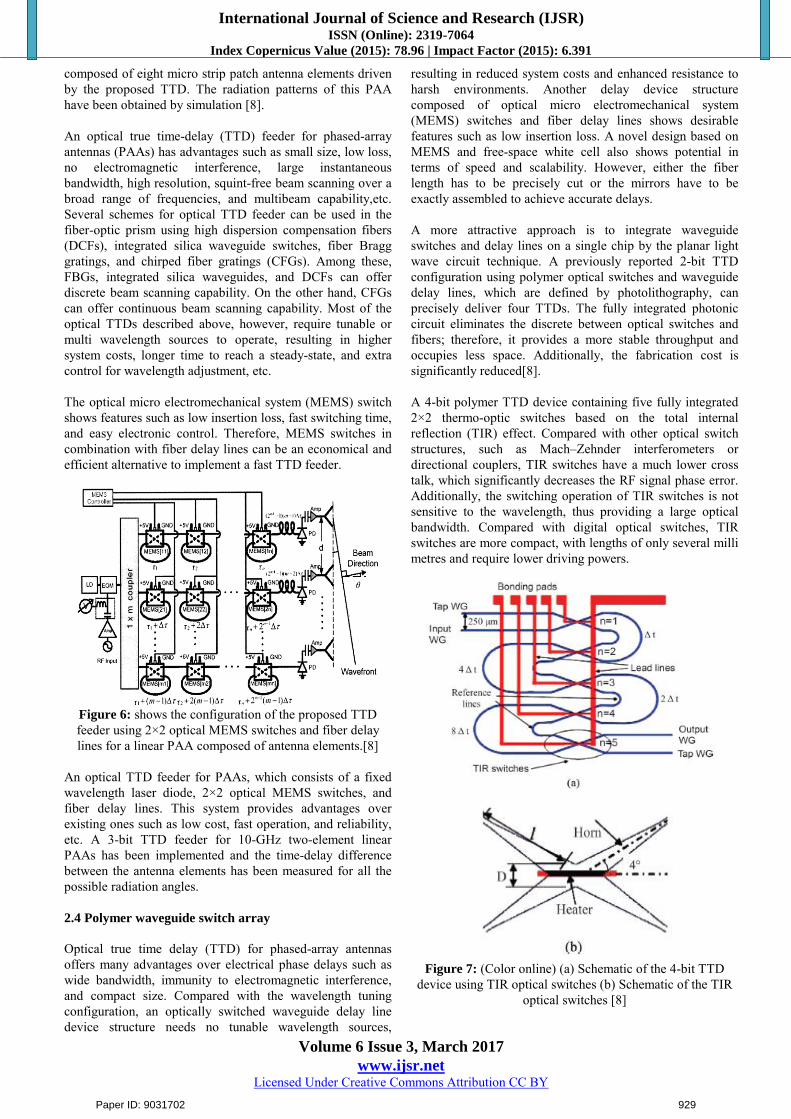
resulting in reduced system costs and enhanced resistance to harsh environments. Another delay device structure composed of optical micro electromechanical system (MEMS) switches and fiber delay lines shows desirable features such as low insertion loss. A novel design based on MEMS and free-space white cell also shows potential in terms of speed and scalability. However, either the fiber length has to be precisely cut or the mirrors have to be exactly assembled to achieve accurate delays. A more attractive approach is to integrate waveguide switches and delay lines on a single chip by the planar light wave circuit technique. A previously reported 2-bit TTD configuration using polymer optical switches and waveguide delay lines, which are defined by photolithography, can precisely deliver four TTDs. The fully integrated photonic circuit eliminates the discrete between optical switches and fibers; therefore, it provides a more stable throughput and occupies less space. Additionally, the fabrication cost is significantly reduced[8]. A 4-bit polymer TTD device containing five fully integrated 2×2 thermo-optic switches based on the total internal reflection (TIR) effect. Compared with other optical switch structures, such as Mach–Zehnder interferometers or directional couplers, TIR switches have a much lower cross talk, which significantly decreases the RF signal phase error. Additionally, the switching operation of TIR switches is not sensitive to the wavelength, thus providing a large optical bandwidth. Compared with digital optical switches, TIR switches are more compact, with lengths of only several milli metres and require lower driving powers.
Figure 7: (Color online) (a) Schematic of the 4-bit TTD
device using TIR optical switches (b) Schematic of the TIR optical switches [8]
Paper ID: 9031702 929

International Journal of Science and Research (IJSR) ISSN (Online): 2319-7064
Index Copernicus Value (2015): 78.96 | Impact Factor (2015): 6.391
Volume 6 Issue 3, March 2017
www.ijsr.net Licensed Under Creative Commons Attribution CC BY
Figure 8: (Color online) Chip die of the 4-bit TTD device
with an enlarged view of the optical switch.[8] The configuration of the proposed TTD device is shown in Fig.7(a). The device is composed of input–output waveguides, five 2×2 TIR thermo-optic switches, four reference lines, and four delay lines, which give 16(24) delay combinations. The TIR switches have a 250μm waveguide separation and 4° half branch angle, as Fig.4.7 (b) shows. Fig.4.7 shows the fabricated 4-bit TTD device with an enlarged view of the TIR thermo-optic switch. The chip die dimension is 21.7 mm × 13.7 mm. The fully-integrated 4-bit TTD module using TIR switches exhibits accurate delays, low power consumption, wavelength insensitivity, small chip size and low fabrication costs. The insertion loss at the wavelength of 1550nm is 13.2 to 16.6dB, depending on the delay paths and the states of optical switches. The switching time of the TIR switches is below 3ms. Design of n bits time delays can be possible where n is a finite integer[8]. 2.5 Ring Resonator based optical beam forming
Integrated optical beam forming networks (IOBFNs) offer many advantages for phased array applications. ORR-based true-time-delay units can be cascaded in a binary tree topology and tuned for continuously-adjustable broadband time delay. Nonetheless, with large number of antenna elements, the IOBFN may become very complex. A novel idea is proposed to exploit the frequency periodicity of the ORRs and the WDM technique to achieve multiple-signal-paths on a single beam former, thus reducing complexity and costs.[9]. Phased arrays antennas offer a number of advantages: electronic beam forming (beam shaping and beam steering), multi beaming and interference nulling capability. In practice, their performances are limited by the characteristics of the beam forming network (BFN) used. A possible improvement to the limitations of all-electronic BFNs can be achieved integrating electronics and photonics by realizing an optical beam forming network (OBFN). This, in principle,
provides large bandwidths, RF frequency transparency, True Time Delay (squint-free) characteristic over the band of interest, EMI immunity, compactness and light weight, thus allowing critical size and weight applications (e.g. aerospace). True time delays (TTD) realized with optical ring resonators. For an OBFN it is desirable to have two basic features: a squint-free behaviour, achievable by using true time delays, and a continuously tunable delay operation. For this reason, optical ring resonators (ORR) appear to be good candidates to realize the delay elements. Ideal lossless ORRs are optical all-pass filters, characterized by a unity magnitude response and continuously tunable group delay response, which represents the effective delay to the radiofrequency (RF) signal that is modulated on the optical carrier. ORR-based OBFN using multiple wavelengths- The basic idea is to create multiple signal paths on the same beam former. In this way, a single delay line carries the signal of different antenna elements, thus significantly reducing the network complexity and, in turn, the number of rings and heaters required. This idea is made possible by the exploitation of the frequency-periodic behaviour of the ORRs used as units. Then, by using multi-wavelength lasers and fast integrated modulators, it is possible to multiplex signals from different antenna elements on a single path, delaying them of the same amount. This multiplexing technique is an optical wavelength division multiplexing (WDM).
Figure 9: Optical ring resonator (ORR) used as true time
delay (TTD) unit. Tuning parameters (a) and spectral characteristics (b)[9]
Figure 10: OBFN binary-tree topology[9]
Paper ID: 9031702 930

International Journal of Science and Research (IJSR) ISSN (Online): 2319-7064
Index Copernicus Value (2015): 78.96 | Impact Factor (2015): 6.391
Volume 6 Issue 3, March 2017
www.ijsr.net Licensed Under Creative Commons Attribution CC BY
As can be seen in the schematic, this technique allows a dramatic reduction in the number of rings required, especially in the case of large number of elements N. As a direct consequence, we achieve a reduction in complexity, in area occupation (the ring dimensions are the limiting factor), in power and heat dissipation (drop in the number of heaters). A novel idea towards the simplification of an existing OBFN has been proposed. Exploiting the frequency-periodic behaviour of the ORR-based delay units and filters, it is possible to realize a WDM-based multi-signal-path OBFN, thus reducing system complexity and cost and making possible an integrated realization of a single-chip OBFN for large arrays or multiple-beam applications[9]. 2.6 Photonic crystal fiber(PCF) based delay line
PHASED-ARRAY ANTENNA (PAA) systems have many advantages over mechanically steered antenna arrays in terms of speed, sensitivity, and size. However, most of phased array antenna radar architectures suffer from problems of being bulky, sensitive to electromagnetic interference (EMI), beam squint effect, and limited bandwidth due to the installation of large amount of electrical cables and microwave phase-shifting devices. Today‟s phased-array radar technologies call for frequency independent beam steering, compact and light weight systems, large instantaneous bandwidth, and EMI free performance [10]. These features can be realized by using optical true-time delay (TTD) techniques. Furthermore, systems with TTD have the intrinsic capability of multi beam operation due to the fact that the optical signals with different optical wavelengths can propagate through a fiber without interfering with each other, for which the widely used dense wavelength division multiplexing (DWDM) system is an illustrative example. Many optical schemes have been proposed to take advantages of a photonic feed for true-time delay (TTD), including acousto-optic (AO) integrated circuit technique, Fourier optics technique, bulky optics technique, dispersive fiber technique, fiber grating technique, and substrate guided wave technique of these techniques, the dispersive fiber technique can reduce the size and weight of the overall system by a significant factor. Conventional systems use single-mode fibers (SMF) as delay lines to implement the dispersive fiber technique. Since the dispersion coefficient D, of SMF is small (18 ps/nm/km @1550 nm), longer lengths of fiber are generally required to generate large time delay values. One alternative to solve this problem is to use highly dispersive photonic crystal fibers (PCF), which can be designed to have very large dispersion values compared to a conventional SMF. By using such highly dispersive photonic crystal fibers as delay lines, we can reduce the length of the fiber dramatically compared to conventional SMF based systems. Working principle of highly dispersive PCF – The PCF structure is based on a dual concentric core configuration. The inner and outer cores are made up of doped silica rods which have a higher refractive index compared to background silica. The refractive index of the inner core is slightly greater than that of the outer core. This
concentric-core PCF with a cross section shown in Fig.11 [16], can support two super modes just like in a directional coupler, which are designed to be nearly phase matched at a wavelength of = 0 .The high dispersion in such a PCF arises from the fact that when < 0,most of the mode energy is strongly confined in the inner core, and when > 0, most of the mode energy stays in the outer core. Near the phase-matched wavelength, there is a strong coupling between the two modes and a part of mode energy is in the inner core and a part of it is in the outer core. This redistribution of mode energy causes the refractive index to change rapidly with wavelength leading to a very high dispersion value near the phase matched wavelength.
Figure 11: Structure for simultaneous transmission of
multiple beams, EOM: EDFA, TTD. The cross-sectional schematic view of the PCF is also shown.[10]
The PCF has a chromatic dispersion coefficient of -600 ps/nm/km, measured at a wavelength of 1550 nm. The dispersion value of the PCF is 33 times larger compared to that of a conventional SMF which is 18 ps/nm/km at 1550 nm. This means that we can shrink the length of the fiber used in this system by a factor of 33 compared to the system using SMF alone, making the system compact and light weight. An optical beam former in the transmitting and receiving mode, employing highly dispersive PCF as TTD elements. Dual-beam operation in the transmitting and receiving modes are demonstrated for RF frequencies of 8.4 and 12 GHz. Utilization of short lengths of highly dispersive PCF in the TTD lines makes the overall system compact and less complex. Such a compact, lightweight system, with the capability of multiple beam transmission and reception, is highly attractive for military and commercial applications[10]. The structure and working demonstration of multiple beam transmission: Using the PCF-based TTD module, multiple-beam transmission can be realized by using the scheme as shown in Fig.11.A general system is shown wherein a multiple number (M) of RF signals are transmitted simultaneously using an antenna array having N elements. A single set of TTD lines generates the required time delay values for each element in the antenna array. External cavity tunable lasers are used to generate a multiple number of optical carrier waves with
Paper ID: 9031702 931
International Journal of Science and Research (IJSR) ISSN (Online): 2319-7064
Index Copernicus Value (2015): 78.96 | Impact Factor (2015): 6.391
Volume 6 Issue 3, March 2017
www.ijsr.net Licensed Under Creative Commons Attribution CC BY
wavelengths 1 to M. RF signals with different frequencies are modulated onto these optical carrier waves using electro optic modulators (EOM). After passing through the EOMs, the optical carrier waves are combined together through an M-to-1 combiner and amplified using an erbium-doped fiber amplifier (EDFA). A 1-to-N optical power splitter divides the amplified optical signal to N TTD lines. Each TTD line has an equal length and consists of different lengths of PCF and SMF segments. The lengths are chosen in such a way that at a wavelength of 0, the nominal delay through each TTD line is the same and the beam is radiated broadside at the antenna array. For wavelengths greater than or less than 0 , different time delays are induced in each TTD line, with a constant time delay difference between adjacent channels at each wavelength, and the beam is steered at an angle θ given by
(4) For N TTD lines having PCF segments of lengths L1, L2, L3......and LN , respectively, as shown in Fig.4.11 The additional time delay generated in a delay line having PCF segment of length Li is given by
(5) The first term is contributed by the PCF section and the second term by the conventional single mode fiber. Since the dispersion coefficient of the PCF is much larger compared to that of the SMF, for a fixed wavelength , the difference of time delays between different channels are only determined by the lengths of the PCF segments. Since the dispersion coefficient of the PCF is much larger compared to that of the SMF, for a fixed wavelength difference of time delays between different channels are only determined by the lengths of the PCF segments. Therefore, by making the lengths of the PCF an arithmetic sequence, we can achieve equal time delay differences between adjacent TTD lines at any given wavelength, thus, forming a wavelength-tuned TTD line. After the optical signals pass through the TTD lines, they are converted back to electrical signals at the photo detector bank. These electrical signals now provide the phase information for the antenna array. Since for a fixed optical wave length, the time delay is only related to the lengths of PCF segments, the delay time of the each output electrical signal is controlled continuously by tuning the optical wavelengths. Each optical wavelength creates a time delay set corresponding to a specific steering angle as given by Eq.(4). By injecting laser beams with multiple wavelengths simultaneously, one can generate equivalent number of independently steered RF far field patterns at the same time due to the squint-free nature of the TTD lines.
2.7 Photonic Microwave Delay line using Mach-Zehnder
Modulator
All optical microwave signal processing was proposed by Wilner and Van den Heuvel that optical fibers could be utilized as delay lines for signal processing, since optical fibers have low loss and large bandwidth. In the generic photonic microwave delay line filter w ith a finite impulse response (FIR) there will be optical interference and generic photonic microwave delay line using TTD as shown in Fig.12.[5] In the generic photonic microwave delay line the key device in a photonic microwave filter is the optical delay-line module, which can be implemented using optical couplers, FBGs, arrayed waveguide (AWG) ,Mach-Zehnder lattices, or a length of dispersive fiber. To avoid optical interference, most of the proposed filters are operating in the incoherent regime; It is known a photonic microwave delay-line filter operating in the incoherent regime would have all-positive tap coefficients. Based on signal processing theory, an all-positive-coefficient microwave delay-line filter would only operate as a low-pass filter. To overcome this limitation, considerable efforts have been taken to design and implement a photonic microwave delay line filter with negative or complex tap coefficients, to achieve band pass filtering functionality in the incoherent regime.
Figure 12: A diagram showing a generic photonic
microwave delay-line filter with a finite impulse response[5]
Figure 13: A photonic microwave delay-line filter with a
negative coefficient using differential detection. MZM: Mach–Zehnder modulator[5]
A straightforward way to generate a negative coefficient is to use differential detection. As shown in Fig.13[5], the light wave from an optical source is modulated by a microwave signal, which is then time delayed by optical fiber delay lines with a time delay difference of τ. The output signals from the fiber delay lines are fed to a differential photo-detection module, which consists of two matched photo detectors with the detected microwave signals combined and subtracted electrically, leading to the generation of a positive and a negative coefficient. In this approach, the negative coefficient was not generated directly in the optical domain, the filter is
Paper ID: 9031702 932

International Journal of Science and Research (IJSR) ISSN (Online): 2319-7064
Index Copernicus Value (2015): 78.96 | Impact Factor (2015): 6.391
Volume 6 Issue 3, March 2017
www.ijsr.net Licensed Under Creative Commons Attribution CC BY
not all-optical, but hybrid. The two-tap photonic microwave delay-line filter shown in Fig.4.13 can be extended to have multiple taps if the single-wavelength source is replaced by a multiwavelength source and the 3-dB coupler is replaced by a WDM demultiplexer[5].
2.8 Optical Mux/Demux based delay line
Multiwavelength integrated optical beam former based on wavelength division multiplexing for 2D phased array antennas was demonstrated in 2014[11]. Integrated optical beam former is explained here. This optical beam former is based on multiwavelength „WDM‟ Technology. Multiple signal path on an individual beam former channel. This approach reduces network complexity and foot print on the wafer. An ultra low loss triplex waveguide platform with (CMOS) compatible fabrication equipment. When there are large number of antenna elements (AE), if we use a single delay line for every element it increases complexity. If we use WDM signal, it can be used for beam forming multiple elements. Fig.14(a) depicts the multi wavelength beam former for 4×4 array when MZI is used. A multi wavelength optical beam former can be designed using a different architecture such as combiner/splitter. This is shown in the Fig.14b. This OBFN consists of 7 segments. The MWL-OBFN is composed by seven cascaded sections. (1) Optical phase shifter section I (2) Horizontal beam forming section (3) Optical demultiplexer (4) SCT section (5) Optical phase shifter Section II (6) Vertical beam forming section (7) Optical sideband filter. Vertical and horizontal beam forming is achieved using this BFN. It functions as follows.
(a)
(b)
Figure 14 (a): Schematic representation of the multiwavelength, multiple-signal-path OBFN, intended to
feed a 4×4 planar antenna array (b) 4×4 array with separable illumination and corresponding Beam former-The MWL-OBFN
[11].
MWL-OBFN has been designed according to the schematic shown in Fig.14(a).To feed a 16 elements antenna array. The chip has only four inputs, each of them carrying the signals originating from four different antenna elements (for a total of 16 AEs), which are wavelength multiplexed using different optical carriers with a channel spacing Δf = 100 GHz. After passing through independent optical phase shifters (1), in the horizontal beam forming section (2), those signals are delayed with respect to each other by the delay units τ1 and τ2 and then optically combined. This allows horizontal beam steering of the main lobe of the generated antenna pattern. The combined output is then applied to a 1×4 demultiplexer (DEMUX, 3). Each wavelength is used to modulate the signals of the same row.(see Fig.14(b) As a consequence, each output of the DEMUX carries the combination of signals received by the antenna elements of the same row. Those signals are then applied to the second part of the MWL-OBFN, namely the vertical beam forming section (6), where they are delayed with respect to each other by the delay units τ1 and τ2.This operation corresponds to the vertical beam steering. The horizontal and vertical beam steering sections have symmetric binary tree architecture [11]. 2.9 PCW based AWG Demux /TTD
Figure 15: Photonic Crystal Waveguide based True Time
Delay Line[12] Light enters the Multi mode interference coupler through waveguide. In the MMI region the light gets diverged and enters the array of waveguide. The light in the array section travels with different velocities and incidents on the image plane (output coupler). For different wavelengths the position of the spot moves along the image plane. The output of this device is fed to the photo detector and used for beam forming .Since the device is behaving like a phasar different phase shifts can be obtained. There are two types of photonic crystal: 1. Air holes in dielectric background 2. Dielectric rod in air Dielectric rod guides TM wave & air holes in dielectric background guides TE wave. This crystal guides light only when a defect is created. The removal of the air hole or dielectric rod is known as defect. It can be a point defect where a single air hole or single rod is removed. This is known as cavity effect.In some cases the rows of air holes or dielectric rods are removed. This is known as line defect by combining point defect & line defect number of photonic devices can be designed such as wave
Paper ID: 9031702 933

International Journal of Science and Research (IJSR) ISSN (Online): 2319-7064
Index Copernicus Value (2015): 78.96 | Impact Factor (2015): 6.391
Volume 6 Issue 3, March 2017
www.ijsr.net Licensed Under Creative Commons Attribution CC BY
guides, power splitters, couplers, resonators, sources etc. E.g. butterfly, peacock feather are natural photonic crystals 2D Photonic Crystal:
Figure 16: 2D Photonic Crystal
They are artificially created semiconductor crystal. Photonic crystal” has two requirements: high index contrast and 1D, 2D or 3D periodic structure. TE or TM Photonic bandgap. Such that the operating frequency falls within the PBG. By creating a point defect and line defect a cavity or waveguide can be created. By combining line and point defect number of PC devices such as waveguides, filters, modulators etc. can be designed [12]. 2.10 Sub wavelength grating enabled on-chip ultra-
compact optical true time delay line
Optical TTD line based on variable length, variable index and variable wavelength as shown in Fig.17
Figure 17: Illustration of the conventional approach for
wavelength- variable ODL (a),the conventional approach for length-variable OTTDL (b), and our proposed approach of
index- variable OTTDL (c). [13] In Fig.17(a) different wavelengths are fed to the combiner. Because of the variation in the group velocity different phase shifts are obtained. These results in a time delay Δt between
optical pulses. In the Fig.17(b) there is a variation in the propagation length due to which Δt is varied Δt =Δ(L/Vg) In these two approaches resonance enhancements is done. Physically, the length of delay medium (waveguide) is enhanced to a cavity structure. In Fig.17(c) an array of waveguides are used whose width linearly varied, due to which there is a phase shift between the optical pulses. 3. Discussions and Conclusions In this review paper various types of True Time Delay Lines are discussed. Miniaturisation and the concepts of on chip integration is of interest in the present scenario. Mathematical modelling of these devices are ignored here. However the qualitative analysis presented here enables to understand the concept of beam steering by combining microwave and photonics. Furthermore TTD using photonic crystal fiber and photonic crystal waveguide gives an exposure to the cutting edge research in the field of Microwave Photonics. References
[1] Maurizio Burla,David A. I. Marpaung,Leimeng Zhuang,Muhammad Rezaul Khan,Arne Leinse, Willem Beeker,Marcel Hoekman,Ren´e G. Heideman, and Chris G. H.Roeloffzen, “Multiwavelength-Integrated Optical Beamformer Based on Wavelength Division Multiplexing for 2-D Phased Array Antennas”, J. Lightw. Technol,,vol. 32, NO. 20, pp 3509- 3518, October 15, 2014
[2] Sylvain Combri´e, Pierre Colman_, Ga¨elle Lehoucq, Alfredo De Rossi, “200ps compact tunable true-time delay line for Microwave photonic applications ”, Advanced Photonics Congress,pp 1-2 © 2012 OSA
[3] Y. Arakawa, T. Nakamura, Y. Urino, and T. Fujita, “Silicon photonics for next generation system integration platform,” IEEE Commun. Mag. 51(3), pp72– 7 ,2013.
[4] J. Xie, L. Zhou, Z. Li, J. Wang, and J. Chen, “Seven-bit reconfigurable optical true time delay line based on silicon integration,” Optics Express, vol. 22, no. 19, pp. 22707–22715, 2014.
[5] Jianping Yao,“Microwave Photonics”, Journal of Light wave Technolgy, vol. 27, NO. 3,pp 314-335,February 1, 2009.
[6] H. Lee, T. Chen, J. Li, O. Painter, and K. J. Vahala,“Ultra-low-loss optical delay line on a silicon chip,” Nat.Commun.3:867, pp.1-7,May,2012
[7] Siva Yegnanarayanan, P. Trinh, F. Coppinger, and B. Jalali, “Compact silicon-based integrated optical time- delay network”, SPIE.Volume 3160.0277-786X,pp1- 9,1997.
[8] X.Wang, B. Howley, M. Y. Chen, and R. T. Chen, “Phase error corrected 4-bit true time delay module using a cascaded 2×2 polymer waveguide switch array,” Applied Optics letter 46(3),pp.379– 383,2007.
[9] M. Burla et al., “Multiwavelength optical beam forming network with ring resonator-based binary-tree architecture for broadband phased array antenna, systems,” in Proc.LEOS Benelux Symp.,Nov. 27–28, Enschede, The Netherlands, pp 99–102,2008
Paper ID: 9031702 934
International Journal of Science and Research (IJSR) ISSN (Online): 2319-7064
Index Copernicus Value (2015): 78.96 | Impact Factor (2015): 6.391
Volume 6 Issue 3, March 2017
www.ijsr.net Licensed Under Creative Commons Attribution CC BY
[10] Harish Subbaraman, Maggie Yihong Chen, and Ray T. Chen, “Photonic Crystal Fiber-Based True-Time-Delay Beamformer for Multiple RF Beam Transmission and Reception of an X-Band Phased-Array Antenna”, Journal of Light wave Technology, vol. 26,NO. 15, pp 2803-2809,2008.
[11] Maurizio Burla,David A. I. Marpaung,Leimeng Zhuang, Muhammad Rezaul Khan,Arne Leinse, Willem Beeker, Marcel Hoekman, Ren´e G.Heideman, and Chris G. H. Roeloffzen, “Multiwavelength-Integrated Optical Beamformer Based on Wavelength Division Multiplexing for 2-D Phased Array Antennas”, J. Lightw. Technol,,vol. 32,NO. 20, pp.3509- 3518,October,2014
[12] Jyothi Digge, B.U.Rindhe, S.K.Narayankhedkar, “Photonic Crystal based Arrayed Waveguide Grating demultiplexer for Optical Network” IJESIT ,vol.3,pp 358-368,2014
[13] Junjia Wang, Reza Ashrafi, Rhys Adams, Ivan Glesk, Ivana Gasulla, José Capmany & Lawrence R. Chen, “Subwavelength grating enabled on-chip ultra-compact optical true time delay line”, Nat.Commun., 6:30235,10.1038/srep30235,pp 1-10,July,2016
Author Profile
Pradnya Sutar is pursuing her post graduation from Terna Engg. College. Earlier she has worked as a faculty at Gharda Institute of Technology”, Lavel, Maharashtra. Her subject area of interests are
Microwave and Photonics. She is the life member of IETE, New Delhi. She has published many papers in national and international conferences.
Dr. Jyothi Digge is currently working as a Professor in EXTC Dept,Terna Engg. College. She has completed her B.E.(Electronics and Communication Engg.)from SJCE Mysore,1987.She is a ME EXTC topper from
university of Mumbai. She is the recipient of “Goldmedal” at Avishkar 2011 by the Governor of Maharashtra.GOI merit scholarship holder from S.S.C. to B.E. She has published number of papers in the national, international conferences and journals. Her research area of interest lies in photonics, Optical communication, Microwave and MICROWAVE PHOTONICS. She has done funded projects relating to photonic crystal based devices. She has 30 years of experience which includes academics and research.
Paper ID: 9031702 935