TriCore 1 v1.3: Volume1: Core Architecture - CS 4
216
Never stop thinking. User’s Manual, V1.3.5, February 2005 Microcontrollers TriCore™ 1 32-bit Unified Processor Core Volume 1: v1.3 Core Architecture
Transcript of TriCore 1 v1.3: Volume1: Core Architecture - CS 4

N e v e r s t o p t h i n k i n g .
User ’s Manual , V1.3.5, February 2005
Microcontrollers
TriCore™ 132-bit Unif ied Processor Core
Volume 1:v1.3 Core Architecture

Edition 2005-02Published by Infineon Technologies AG,St.-Martin-Strasse 53,81669 München© Infineon Technologies AG 2005.All Rights Reserved.
Attention please!The information herein is given to describe certain components and shall not be considered as a guarantee of characteristics.Terms of delivery and rights to technical change reserved.We hereby disclaim any and all warranties, including but not limited to warranties of non-infringement, regarding circuits, descriptions and charts stated herein.
InformationFor further information on technology, delivery terms and conditions and prices please contact your nearest Infineon Technologies Office (www.Infineon.com).
WarningsDue to technical requirements components may contain dangerous substances. For information on the types in question please contact your nearest Infineon Technologies Office.Infineon Technologies Components may only be used in life-support devices or systems with the express written approval of Infineon Technologies, if a failure of such components can reasonably be expected to cause the failure of that life-support device or system, or to affect the safety or effectiveness of that device or system. Life support devices or systems are intended to be implanted in the human body, or to support and/or maintain and sustain and/or protect human life. If they fail, it is reasonable to assume that the health of the user or other persons may be endangered.

User’s Manual , V1.3.5, February 2005
N e v e r s t o p t h i n k i n g .
Microcontrollers
TriCore™ 132-bit Unif ied Processor Core
Volume1:v1.3 Core Architecture

TriCoreTM is a trademark of Infineon Technologies AG.
TriCore™ 1 User’s ManualRevision History 2005-02 V1.3.5Previous VersionVersion Subjects (major changes since last revision)1.3.0 First release v1.3 architecture (Jan 2000).1.3.2 General release of v1.3 architecture (August 2000).1.3.3 Revision of chapters 3, 6, 8 and 9. Addition of appendices.1.3.5 New information, general revision and restructuring of instruction set.
Information split into two volumes: Core Architecture and Instruction Set.
We Listen to Your CommentsIs there any information in this document that you feel is wrong, unclear or missing?Your feedback will help us to continuously improve the quality of our documentation.Please send feedback (including a reference to this document) to:[email protected]

TriCore™ 132-bit Unified Processor Core
Contents
1 Preface . . . . . . . . . . . . . . . . . . . . . . . . . . . . . . . . . . . . . . . . . . . . . . . . . . 1-11.1 Text Conventions . . . . . . . . . . . . . . . . . . . . . . . . . . . . . . . . . . . . . . . . . . . 1-2
2 Architecture Overview . . . . . . . . . . . . . . . . . . . . . . . . . . . . . . . . . . . . . . 2-12.1 Introduction . . . . . . . . . . . . . . . . . . . . . . . . . . . . . . . . . . . . . . . . . . . . . . . 2-12.1.1 Feature Summary . . . . . . . . . . . . . . . . . . . . . . . . . . . . . . . . . . . . . . . . 2-22.2 Programming Model . . . . . . . . . . . . . . . . . . . . . . . . . . . . . . . . . . . . . . . . 2-22.2.1 Architectural Registers . . . . . . . . . . . . . . . . . . . . . . . . . . . . . . . . . . . . . 2-32.2.2 Data Types . . . . . . . . . . . . . . . . . . . . . . . . . . . . . . . . . . . . . . . . . . . . . 2-42.2.3 Memory Model . . . . . . . . . . . . . . . . . . . . . . . . . . . . . . . . . . . . . . . . . . . 2-52.2.4 Addressing Modes . . . . . . . . . . . . . . . . . . . . . . . . . . . . . . . . . . . . . . . . 2-52.3 Tasks and Contexts . . . . . . . . . . . . . . . . . . . . . . . . . . . . . . . . . . . . . . . . . 2-62.4 Interrupt System . . . . . . . . . . . . . . . . . . . . . . . . . . . . . . . . . . . . . . . . . . . 2-72.4.1 Interrupt Priority . . . . . . . . . . . . . . . . . . . . . . . . . . . . . . . . . . . . . . . . . . 2-72.5 Trap System . . . . . . . . . . . . . . . . . . . . . . . . . . . . . . . . . . . . . . . . . . . . . . 2-82.6 Protection System . . . . . . . . . . . . . . . . . . . . . . . . . . . . . . . . . . . . . . . . . . 2-82.7 Memory Management Unit . . . . . . . . . . . . . . . . . . . . . . . . . . . . . . . . . . . 2-92.8 Core Debug Controller . . . . . . . . . . . . . . . . . . . . . . . . . . . . . . . . . . . . . . 2-10
3 Programming Model . . . . . . . . . . . . . . . . . . . . . . . . . . . . . . . . . . . . . . . 3-13.1 Data Types . . . . . . . . . . . . . . . . . . . . . . . . . . . . . . . . . . . . . . . . . . . . . . . 3-13.1.1 Boolean . . . . . . . . . . . . . . . . . . . . . . . . . . . . . . . . . . . . . . . . . . . . . . . . 3-13.1.2 Bit String . . . . . . . . . . . . . . . . . . . . . . . . . . . . . . . . . . . . . . . . . . . . . . . 3-13.1.3 Byte . . . . . . . . . . . . . . . . . . . . . . . . . . . . . . . . . . . . . . . . . . . . . . . . . . . 3-13.1.4 Signed Fraction . . . . . . . . . . . . . . . . . . . . . . . . . . . . . . . . . . . . . . . . . . 3-23.1.5 Address . . . . . . . . . . . . . . . . . . . . . . . . . . . . . . . . . . . . . . . . . . . . . . . . 3-23.1.6 Signed and Unsigned Integers . . . . . . . . . . . . . . . . . . . . . . . . . . . . . . 3-23.1.7 IEEE-754 Single-Precision Floating-Point Number . . . . . . . . . . . . . . . 3-23.2 Data Formats . . . . . . . . . . . . . . . . . . . . . . . . . . . . . . . . . . . . . . . . . . . . . . 3-23.2.1 Alignment Requirements . . . . . . . . . . . . . . . . . . . . . . . . . . . . . . . . . . . 3-43.2.2 Byte Ordering . . . . . . . . . . . . . . . . . . . . . . . . . . . . . . . . . . . . . . . . . . . . 3-53.3 Memory Model . . . . . . . . . . . . . . . . . . . . . . . . . . . . . . . . . . . . . . . . . . . . . 3-63.4 Addressing Modes . . . . . . . . . . . . . . . . . . . . . . . . . . . . . . . . . . . . . . . . . . 3-73.4.1 Absolute Addressing . . . . . . . . . . . . . . . . . . . . . . . . . . . . . . . . . . . . . . 3-83.4.2 Base + Offset Addressing . . . . . . . . . . . . . . . . . . . . . . . . . . . . . . . . . . 3-83.4.3 Pre-Increment and Pre-Decrement Addressing . . . . . . . . . . . . . . . . . . 3-83.4.4 Post-Increment and Post-Decrement Addressing . . . . . . . . . . . . . . . . 3-93.4.5 Circular Addressing . . . . . . . . . . . . . . . . . . . . . . . . . . . . . . . . . . . . . . . 3-93.4.6 Bit-Reverse Addressing . . . . . . . . . . . . . . . . . . . . . . . . . . . . . . . . . . . 3-113.4.7 Synthesized Addressing Modes . . . . . . . . . . . . . . . . . . . . . . . . . . . . 3-12
User’s Manual I-1 V1.3.5, 2005-02

TriCore™ 132-bit Unified Processor Core
Contents
4 Core Registers . . . . . . . . . . . . . . . . . . . . . . . . . . . . . . . . . . . . . . . . . . . . 4-14.1 ENDINIT Protection . . . . . . . . . . . . . . . . . . . . . . . . . . . . . . . . . . . . . . . . . 4-14.2 Core Register Table . . . . . . . . . . . . . . . . . . . . . . . . . . . . . . . . . . . . . . . . . 4-14.3 General Purpose Registers (GPRs) . . . . . . . . . . . . . . . . . . . . . . . . . . . . 4-74.4 Core Special Function Register (CSFR) Definitions . . . . . . . . . . . . . . . . 4-94.5 Program State Information . . . . . . . . . . . . . . . . . . . . . . . . . . . . . . . . . . . 4-104.5.1 Program Counter (PC) . . . . . . . . . . . . . . . . . . . . . . . . . . . . . . . . . . . . 4-104.5.2 Program Status Word (PSW) . . . . . . . . . . . . . . . . . . . . . . . . . . . . . . . 4-114.5.3 Previous Context Information Register (PCXI) . . . . . . . . . . . . . . . . . 4-164.6 Context Management Registers . . . . . . . . . . . . . . . . . . . . . . . . . . . . . . 4-174.6.1 Free CSA List Head Pointer (FCX) . . . . . . . . . . . . . . . . . . . . . . . . . . 4-184.6.2 Previous Context Pointer (PCX) . . . . . . . . . . . . . . . . . . . . . . . . . . . . 4-194.6.3 Free CSA List Limit Pointer (LCX) . . . . . . . . . . . . . . . . . . . . . . . . . . . 4-204.7 Stack Management . . . . . . . . . . . . . . . . . . . . . . . . . . . . . . . . . . . . . . . . 4-214.7.1 Address Register A[10] (SP) . . . . . . . . . . . . . . . . . . . . . . . . . . . . . . . 4-224.7.2 Interrupt Stack Pointer (ISP) . . . . . . . . . . . . . . . . . . . . . . . . . . . . . . . 4-224.8 Interrupt and Trap Control . . . . . . . . . . . . . . . . . . . . . . . . . . . . . . . . . . . 4-234.8.1 Interrupt Control Register (ICR) . . . . . . . . . . . . . . . . . . . . . . . . . . . . . 4-234.8.2 Base Interrupt Vector Table Pointer (BIV) . . . . . . . . . . . . . . . . . . . . . 4-254.8.3 Base Trap Vector Table Pointer (BTV) . . . . . . . . . . . . . . . . . . . . . . . 4-264.9 System Control Registers (SYSCON) . . . . . . . . . . . . . . . . . . . . . . . . . . 4-274.10 ID Registers . . . . . . . . . . . . . . . . . . . . . . . . . . . . . . . . . . . . . . . . . . . . . . 4-284.10.1 CPU Identification Register (CPU_ID) . . . . . . . . . . . . . . . . . . . . . . . . 4-284.11 Interrupt Registers . . . . . . . . . . . . . . . . . . . . . . . . . . . . . . . . . . . . . . . . . 4-294.12 Memory Protection Registers . . . . . . . . . . . . . . . . . . . . . . . . . . . . . . . . 4-294.13 Memory Management Unit Registers . . . . . . . . . . . . . . . . . . . . . . . . . . 4-294.14 Core Debug Controller Registers . . . . . . . . . . . . . . . . . . . . . . . . . . . . . . 4-30
5 Tasks and Functions . . . . . . . . . . . . . . . . . . . . . . . . . . . . . . . . . . . . . . . 5-15.1 Upper and Lower Contexts . . . . . . . . . . . . . . . . . . . . . . . . . . . . . . . . . . . 5-15.1.1 Context Save Area . . . . . . . . . . . . . . . . . . . . . . . . . . . . . . . . . . . . . . . . 5-35.2 Task Switching Operation . . . . . . . . . . . . . . . . . . . . . . . . . . . . . . . . . . . . 5-45.2.1 Save and Restore Context Operations . . . . . . . . . . . . . . . . . . . . . . . . 5-55.3 Context Save Areas (CSAs) and Context Lists . . . . . . . . . . . . . . . . . . . . 5-55.4 Context Switching with Interrupts and Traps . . . . . . . . . . . . . . . . . . . . . . 5-75.5 Context Switching for Function Calls . . . . . . . . . . . . . . . . . . . . . . . . . . . . 5-85.6 Context Save and Restore Examples . . . . . . . . . . . . . . . . . . . . . . . . . . . 5-95.6.1 Context Save . . . . . . . . . . . . . . . . . . . . . . . . . . . . . . . . . . . . . . . . . . . . 5-95.6.2 Context Restore . . . . . . . . . . . . . . . . . . . . . . . . . . . . . . . . . . . . . . . . . 5-11
6 Interrupt System . . . . . . . . . . . . . . . . . . . . . . . . . . . . . . . . . . . . . . . . . . 6-16.1 Service Request Node (SRN) . . . . . . . . . . . . . . . . . . . . . . . . . . . . . . . . . 6-16.1.1 Service Request Control Register (SRC) . . . . . . . . . . . . . . . . . . . . . . 6-36.2 Interrupt Control Unit (ICU) . . . . . . . . . . . . . . . . . . . . . . . . . . . . . . . . . . . 6-6
User’s Manual I-2 V1.3.5, 2005-02

TriCore™ 132-bit Unified Processor Core
Contents
6.2.1 ICU Interrupt Control Register (ICR) . . . . . . . . . . . . . . . . . . . . . . . . . . 6-76.2.2 Interrupt Control Unit Operation . . . . . . . . . . . . . . . . . . . . . . . . . . . . . . 6-76.2.3 Arbitration Scheme . . . . . . . . . . . . . . . . . . . . . . . . . . . . . . . . . . . . . . . 6-86.3 Entering an Interrupt Service Routine (ISR) . . . . . . . . . . . . . . . . . . . . . . 6-86.4 Exiting an Interrupt Service Routine (ISR) . . . . . . . . . . . . . . . . . . . . . . . . 6-96.5 Interrupt Vector Table . . . . . . . . . . . . . . . . . . . . . . . . . . . . . . . . . . . . . . 6-106.6 Using the TriCore Interrupt System . . . . . . . . . . . . . . . . . . . . . . . . . . . . 6-126.6.1 Spanning Interrupt Service Routines across Vector Entries . . . . . . . 6-126.6.2 Interrupt Priority Groups . . . . . . . . . . . . . . . . . . . . . . . . . . . . . . . . . . 6-126.6.3 Dividing ISRs into Different Priorities . . . . . . . . . . . . . . . . . . . . . . . . . 6-146.6.4 Using Different Priorities for the Same Interrupt Source . . . . . . . . . . 6-146.6.5 Software-Posted Interrupts . . . . . . . . . . . . . . . . . . . . . . . . . . . . . . . . 6-156.6.6 Interrupt Priority Level One . . . . . . . . . . . . . . . . . . . . . . . . . . . . . . . . 6-15
7 Trap System . . . . . . . . . . . . . . . . . . . . . . . . . . . . . . . . . . . . . . . . . . . . . . 7-17.1 Trap Types . . . . . . . . . . . . . . . . . . . . . . . . . . . . . . . . . . . . . . . . . . . . . . . . 7-17.1.1 Synchronous Traps . . . . . . . . . . . . . . . . . . . . . . . . . . . . . . . . . . . . . . . 7-37.1.2 Asynchronous Traps . . . . . . . . . . . . . . . . . . . . . . . . . . . . . . . . . . . . . . 7-37.1.3 Hardware Traps . . . . . . . . . . . . . . . . . . . . . . . . . . . . . . . . . . . . . . . . . . 7-37.1.4 Software Traps . . . . . . . . . . . . . . . . . . . . . . . . . . . . . . . . . . . . . . . . . . 7-37.1.5 Unrecoverable Traps . . . . . . . . . . . . . . . . . . . . . . . . . . . . . . . . . . . . . . 7-37.2 Trap Handling . . . . . . . . . . . . . . . . . . . . . . . . . . . . . . . . . . . . . . . . . . . . . 7-47.2.1 Trap Vector Format . . . . . . . . . . . . . . . . . . . . . . . . . . . . . . . . . . . . . . . 7-47.2.2 Accessing the Trap Vector Table . . . . . . . . . . . . . . . . . . . . . . . . . . . . . 7-47.2.3 Return Address (RA) . . . . . . . . . . . . . . . . . . . . . . . . . . . . . . . . . . . . . . 7-47.2.4 Trap Vector Table . . . . . . . . . . . . . . . . . . . . . . . . . . . . . . . . . . . . . . . . 7-57.2.5 Initial State upon a Trap . . . . . . . . . . . . . . . . . . . . . . . . . . . . . . . . . . . . 7-67.3 Trap Descriptions . . . . . . . . . . . . . . . . . . . . . . . . . . . . . . . . . . . . . . . . . . . 7-77.3.1 MMU Traps (Trap Class 0) . . . . . . . . . . . . . . . . . . . . . . . . . . . . . . . . . 7-77.3.2 Internal Protection Traps (Trap Class 1) . . . . . . . . . . . . . . . . . . . . . . . 7-77.3.3 Instruction Errors (Trap Class 2) . . . . . . . . . . . . . . . . . . . . . . . . . . . . . 7-87.3.4 Context Management (Trap Class 3) . . . . . . . . . . . . . . . . . . . . . . . . . 7-107.3.5 System Bus and Peripheral Errors (Trap Class 4) . . . . . . . . . . . . . . . 7-127.3.6 Assertion Traps (Trap Class 5) . . . . . . . . . . . . . . . . . . . . . . . . . . . . . 7-137.3.7 System Call (Trap Class 6) . . . . . . . . . . . . . . . . . . . . . . . . . . . . . . . . 7-137.3.8 Non-Maskable Interrupt (Trap Class 7) . . . . . . . . . . . . . . . . . . . . . . . 7-137.3.9 Debug Traps . . . . . . . . . . . . . . . . . . . . . . . . . . . . . . . . . . . . . . . . . . . 7-137.4 Exception Priorities . . . . . . . . . . . . . . . . . . . . . . . . . . . . . . . . . . . . . . . . 7-14
8 Physical Memory Attributes (PMA) . . . . . . . . . . . . . . . . . . . . . . . . . . . 8-18.1 Physical Memory Properties (PMP) . . . . . . . . . . . . . . . . . . . . . . . . . . . . . 8-18.2 Physical Memory Attributes (PMA) . . . . . . . . . . . . . . . . . . . . . . . . . . . . . 8-38.2.1 Physical Memory Attributes of the Address Map . . . . . . . . . . . . . . . . . 8-38.3 Scratchpad RAM . . . . . . . . . . . . . . . . . . . . . . . . . . . . . . . . . . . . . . . . . . . 8-4
User’s Manual I-3 V1.3.5, 2005-02

TriCore™ 132-bit Unified Processor Core
Contents
8.4 Permitted versus Valid Accesses . . . . . . . . . . . . . . . . . . . . . . . . . . . . . . 8-5
9 Memory Protection System . . . . . . . . . . . . . . . . . . . . . . . . . . . . . . . . . 9-19.1 Memory Protection Registers . . . . . . . . . . . . . . . . . . . . . . . . . . . . . . . . . 9-19.1.1 Memory Protection Registers . . . . . . . . . . . . . . . . . . . . . . . . . . . . . . . 9-49.2 Access Permissions for Intersecting Memory Ranges . . . . . . . . . . . . . 9-109.2.1 Example . . . . . . . . . . . . . . . . . . . . . . . . . . . . . . . . . . . . . . . . . . . . . . . 9-109.3 Using the Memory Protection System . . . . . . . . . . . . . . . . . . . . . . . . . . 9-129.3.1 Protection Enable bit . . . . . . . . . . . . . . . . . . . . . . . . . . . . . . . . . . . . . 9-129.3.2 Set Selection . . . . . . . . . . . . . . . . . . . . . . . . . . . . . . . . . . . . . . . . . . . 9-129.3.3 Address Range . . . . . . . . . . . . . . . . . . . . . . . . . . . . . . . . . . . . . . . . . 9-129.3.4 Traps . . . . . . . . . . . . . . . . . . . . . . . . . . . . . . . . . . . . . . . . . . . . . . . . . 9-139.4 Crossing Protection Boundaries . . . . . . . . . . . . . . . . . . . . . . . . . . . . . . 9-13
10 Memory Management Unit (MMU) . . . . . . . . . . . . . . . . . . . . . . . . . . . 10-110.1 Address Spaces . . . . . . . . . . . . . . . . . . . . . . . . . . . . . . . . . . . . . . . . . . . 10-210.2 Address Translation . . . . . . . . . . . . . . . . . . . . . . . . . . . . . . . . . . . . . . . . 10-310.2.1 Address Translation for CSFR Pointers . . . . . . . . . . . . . . . . . . . . . . . 10-310.3 Translation Lookaside Buffers (TLBs) . . . . . . . . . . . . . . . . . . . . . . . . . . 10-410.3.1 TLB Table Entry (TTE) Contents . . . . . . . . . . . . . . . . . . . . . . . . . . . . 10-510.4 Multiple Address Spaces . . . . . . . . . . . . . . . . . . . . . . . . . . . . . . . . . . . . 10-510.5 MMU Traps . . . . . . . . . . . . . . . . . . . . . . . . . . . . . . . . . . . . . . . . . . . . . . 10-510.6 Virtual Mode Protection . . . . . . . . . . . . . . . . . . . . . . . . . . . . . . . . . . . . . 10-710.6.1 Direct Translation . . . . . . . . . . . . . . . . . . . . . . . . . . . . . . . . . . . . . . . . 10-710.6.2 Page Table Entry (PTE) Based Translation . . . . . . . . . . . . . . . . . . . . 10-710.7 Cacheability . . . . . . . . . . . . . . . . . . . . . . . . . . . . . . . . . . . . . . . . . . . . . . 10-710.7.1 Direct Translation Virtual Address Cacheability . . . . . . . . . . . . . . . . . 10-710.7.2 PTE Translation Cacheability . . . . . . . . . . . . . . . . . . . . . . . . . . . . . . 10-710.7.3 Cacheability of a Virtual Address Flow . . . . . . . . . . . . . . . . . . . . . . . 10-810.8 MMU Instructions . . . . . . . . . . . . . . . . . . . . . . . . . . . . . . . . . . . . . . . . . . 10-810.8.1 TLBMAP (TLB Map) . . . . . . . . . . . . . . . . . . . . . . . . . . . . . . . . . . . . . 10-910.8.2 TLBDEMAP (TLB Demap) . . . . . . . . . . . . . . . . . . . . . . . . . . . . . . . . 10-1010.8.3 TLBFLUSH (TLB Flush) . . . . . . . . . . . . . . . . . . . . . . . . . . . . . . . . . . 10-1010.8.4 TLBPROBE (TLB Probe) . . . . . . . . . . . . . . . . . . . . . . . . . . . . . . . . . 10-1110.9 TLB Usage . . . . . . . . . . . . . . . . . . . . . . . . . . . . . . . . . . . . . . . . . . . . . . 10-1210.10 MMU Core Special Function Registers . . . . . . . . . . . . . . . . . . . . . . . . 10-1310.10.1 MMU Configuration Register (MMU_CON) . . . . . . . . . . . . . . . . . . . 10-1310.10.2 Address Space Identifier Register (MMU_ASI) . . . . . . . . . . . . . . . . 10-1510.10.3 Translation Virtual Address Register (MMU_TVA) . . . . . . . . . . . . . 10-1610.10.4 Translation Physical Address Register (MMU_TPA) . . . . . . . . . . . . 10-1710.10.5 Translation Page Index Register (MMU_TPX) . . . . . . . . . . . . . . . . 10-1910.10.6 Translation Fault Page Address Register (MMU_TFA) . . . . . . . . . . 10-20
User’s Manual I-4 V1.3.5, 2005-02

TriCore™ 132-bit Unified Processor Core
Contents
11 Core Debug Controller (CDC) . . . . . . . . . . . . . . . . . . . . . . . . . . . . . . . 11-111.1 Run Control Features . . . . . . . . . . . . . . . . . . . . . . . . . . . . . . . . . . . . . . 11-111.2 Debug Events . . . . . . . . . . . . . . . . . . . . . . . . . . . . . . . . . . . . . . . . . . . . 11-311.2.1 External Debug Event . . . . . . . . . . . . . . . . . . . . . . . . . . . . . . . . . . . . 11-311.2.2 Debug Instruction . . . . . . . . . . . . . . . . . . . . . . . . . . . . . . . . . . . . . . . . 11-311.2.3 MTCR and MFCR Instructions . . . . . . . . . . . . . . . . . . . . . . . . . . . . . . 11-311.2.4 Trigger Event Unit . . . . . . . . . . . . . . . . . . . . . . . . . . . . . . . . . . . . . . . 11-411.2.5 Priority of Debug Events . . . . . . . . . . . . . . . . . . . . . . . . . . . . . . . . . . 11-411.3 Debug Triggers . . . . . . . . . . . . . . . . . . . . . . . . . . . . . . . . . . . . . . . . . . . 11-611.3.1 Combining Debug Triggers . . . . . . . . . . . . . . . . . . . . . . . . . . . . . . . . 11-711.4 Debug Actions . . . . . . . . . . . . . . . . . . . . . . . . . . . . . . . . . . . . . . . . . . . . 11-811.4.1 Update Debug Status Register (DBGSR) . . . . . . . . . . . . . . . . . . . . . 11-811.4.2 Indicate on Core Break-Out Signal . . . . . . . . . . . . . . . . . . . . . . . . . . 11-811.4.3 Indicate on Core Suspend-Out Signal . . . . . . . . . . . . . . . . . . . . . . . . 11-911.4.4 Halt . . . . . . . . . . . . . . . . . . . . . . . . . . . . . . . . . . . . . . . . . . . . . . . . . . 11-911.4.5 Breakpoint Trap . . . . . . . . . . . . . . . . . . . . . . . . . . . . . . . . . . . . . . . . . 11-911.4.6 Breakpoint Interrupt . . . . . . . . . . . . . . . . . . . . . . . . . . . . . . . . . . . . . 11-1011.4.7 Posted Software Events . . . . . . . . . . . . . . . . . . . . . . . . . . . . . . . . . 11-1111.4.8 Interrupts to Other Targets . . . . . . . . . . . . . . . . . . . . . . . . . . . . . . . 11-1111.5 CDC Control Registers . . . . . . . . . . . . . . . . . . . . . . . . . . . . . . . . . . . . 11-1211.5.1 Software Breakpoint Service Request Control Register . . . . . . . . . 11-22
12 Floating Point Unit (FPU) . . . . . . . . . . . . . . . . . . . . . . . . . . . . . . . . . . 12-112.1 Functional Overview . . . . . . . . . . . . . . . . . . . . . . . . . . . . . . . . . . . . . . . 12-112.2 IEEE-754 Compliance . . . . . . . . . . . . . . . . . . . . . . . . . . . . . . . . . . . . . . 12-212.2.1 IEEE-754 Single Precision Data Format . . . . . . . . . . . . . . . . . . . . . . 12-212.2.2 Denormal Numbers . . . . . . . . . . . . . . . . . . . . . . . . . . . . . . . . . . . . . . 12-312.2.3 NaNs (Not a Number) . . . . . . . . . . . . . . . . . . . . . . . . . . . . . . . . . . . . 12-312.2.4 Underflow . . . . . . . . . . . . . . . . . . . . . . . . . . . . . . . . . . . . . . . . . . . . . . 12-412.2.5 Fused MACs . . . . . . . . . . . . . . . . . . . . . . . . . . . . . . . . . . . . . . . . . . . 12-412.2.6 Software Routines . . . . . . . . . . . . . . . . . . . . . . . . . . . . . . . . . . . . . . . 12-512.3 Rounding . . . . . . . . . . . . . . . . . . . . . . . . . . . . . . . . . . . . . . . . . . . . . . . . 12-612.3.1 Round to Nearest: Even . . . . . . . . . . . . . . . . . . . . . . . . . . . . . . . . . . 12-712.3.2 Round to Nearest: Denormals and Zero Substitution . . . . . . . . . . . . 12-712.3.3 Round Towards ± ∞: Denormals and Zero Substitution . . . . . . . . . . 12-812.4 Exceptions . . . . . . . . . . . . . . . . . . . . . . . . . . . . . . . . . . . . . . . . . . . . . . . 12-9
13 Glossary . . . . . . . . . . . . . . . . . . . . . . . . . . . . . . . . . . . . . . . . . . . . . . . . 13-1
14 List of Registers . . . . . . . . . . . . . . . . . . . . . . . . . . . . . . . . . . . . . . . . . . 14-1
15 Index . . . . . . . . . . . . . . . . . . . . . . . . . . . . . . . . . . . . . . . . . . . . . . . . . . . 15-1
User’s Manual I-5 V1.3.5, 2005-02

TriCore™ 132-bit Unified Processor Core
Contents
User’s Manual I-6 V1.3.5, 2005-02

TriCore™ 132-bit Unified Processor Core
Preface
1 PrefaceThis manual describes the TriCore architecture, Infineon’s ground breaking unified,32-bit microcontroller-DSP, single-core architecture optimized for real-time embeddedsystems. This document has been written for system developers and programmers, and hardwareand software engineers. The document has been split into two volumes:• Volume 1 (this volume) provides a detailed description of the Core Architecture and
system interaction.• Volume 2 gives a complete description of the TriCore Instruction Set including
optional extensions for the MMU and FPU.It is important to note that this document describes the TriCore architecture, not animplementation. An implementation may have features and resources which are not partof the Core Architecture. The documentation for that implementation will describe allimplementation specific features.When working with a specific TriCore based product always refer to the appropriatesupporting documentation.
Additional InformationFor the latest documentation and additional TriCore information, please visit the TriCorehome page at:http://www.infineon.com/TriCoreFor information and links to documentation for Infineon products that use TriCore, visit:http://www.infineon.com/32-bit-microcontrollers
User’s Manual 1-1 V1.3.5, 2005-02

TriCore™ 132-bit Unified Processor Core
Preface
1.1 Text ConventionsThis document uses the following text conventions:• The default radix is decimal.
– Hexadecimal constants are suffixed with a subscript letter ‘H’, as in: FFCH.– Binary constants are suffixed with a subscript letter ‘B’, as in: 111B.
• Register reset values are not generally architecturally defined, but require setting onstartup in a given implementation of the architecture. Only those reset values that arearchitecturally defined are shown in this document. Where no value is shown, thereset value is not defined. Refer to the documentation for a specific TriCoreimplementation.
• Units are abbreviated as follows:– MHz = Megahertz.– kBaud, kBit = 1000 characters/bits per second.– MBaud, MBit = 1,000,000 characters per second.– KByte = 1024 bytes.– MByte = 1048576 bytes of memory.– GByte = 1,024 megabytes.
• Data format quantities referenced are as follows:– Byte = 8-bit quantity.– Half-word = 16-bit quantity.– Word = 32-bit quantity.– Double-word = 64-bit quantity.
• Pins using negative logic are indicated by an overbar: BRKOUT.• Where the phrase ‘Reserved Value’ is used, NEVER write to this value.In tables where register bit fields are defined, the conventions shown in Table 1 are usedin this document.
Note: In register layout tables, a ‘Reserved Field’ is indicated with ‘-’ in the Field andType column.
Table 1 Bit Type Abbreviations
Abbreviation Descriptionr Read-only. The bit or bit field can only be read.w Write-only. The bit or bit field can only be written.rw The bit or bit field can be read and written.h The bit or bit field can be modified by hardware (such as a status bit).
‘h’ can be combined with ‘rw’ or ‘r’ bits to form ‘rwh’ or ‘rh’ bits.- Reserved Field. Read value is undefined, must be written with 0.
User’s Manual 1-2 V1.3.5, 2005-02

TriCore™ 132-bit Unified Processor Core
Architecture Overview
2 Architecture OverviewThis chapter gives an overview of the TriCore™ architecture.
2.1 IntroductionTriCore is the first unified, single-core, 32-bit microcontroller-DSP architecture optimizedfor real-time embedded systems. The TriCore Instruction Set Architecture (ISA)combines the real-time capability of a microcontroller, the computational power of aDSP, and the high performance/price features of a RISC load/store architecture, in acompact re-programmable core.
Figure 1 TriCore Architecture Overview
The ISA supports a uniform, 32-bit address space, with optional virtual addressing andmemory-mapped I/O. The architecture allows for a wide range of implementations,ranging from scalar through to superscalar, and is capable of interacting with differentsystem architectures, including multiprocessing. This flexibility at the implementationand system levels allows for different trade-offs between performance and cost at anypoint in time.The architecture supports both 16-bit and 32-bit instruction formats. All instructions havea 32-bit format. The 16-bit instructions are a subset of the 32-bit instructions, chosenbecause of their frequency of use. These instructions significantly reduce code space,lowering memory requirements, system and power consumption.Real-time responsiveness is largely determined by interrupt latency and context-switchtime. The high-performance architecture minimizes interrupt latency by avoiding longmulti-cycle instructions and by providing a flexible hardware-supported interruptscheme. The architecture also supports fast-context switching.
Bit-field, Bit-logicalMin/Max ComparisonBranch
MAC, Saturated Math,DSP Addressing Modes,SIMD Packed Arithmetic
Arithmetic, LogicAddress Arithmetic& Comparison,Load/Store, Context Switch
Load/StoreArithmeticBranch
FloatingPoint
MCA05096
User’s Manual 2-1 V1.3.5, 2005-02

TriCore™ 132-bit Unified Processor Core
Architecture Overview
2.1.1 Feature SummaryThe key features of the TriCore Instruction Set Architecture (ISA) are:• 32-bit architecture.• 4 GBytes of address space.• 16-bit and 32-bit instructions for reduced code size.• Most instructions executed in one cycle.• Branch instructions (using branch prediction).• Low interrupt latency with fast automatic context switch using wide pathway to
on-chip memory.• Dedicated interface to application-specific co-processors to allow the addition of
customised instructions.• Zero overhead loop capabilities.• Dual single-clock-cycle 16×16-bit multiply-accumulate unit (with optional saturation).• Optional Floating-Point Unit (FPU) and Memory Management Unit (MMU).• Extensive bit handling capabilities.• Single Instruction Multiple Data (SIMD) packed data operations (2×16-bit or 4×8-bit
operands).• Flexible interrupt prioritization scheme.• Byte and bit addressing.• Little-endian byte ordering for data memory and CPU registers.• Memory protection.• Debug support.
2.2 Programming ModelThis section covers aspects of the architecture that are visible to software:• Architectural Registers page 2-3.• Data Types page 2-4.• Memory Model page 2-5.• Addressing Modes page 2-5.The Programming Model is described in detail in the chapter ProgrammingModel, page 3-1.
User’s Manual 2-2 V1.3.5, 2005-02

TriCore™ 132-bit Unified Processor Core
Architecture Overview
2.2.1 Architectural RegistersThe architectural registers consist of:• 32 General Purpose Registers (GPRs).• Program Counter (PC).• Two 32-bit registers containing status flags, previous execution information and
protection information (PCXI - Previous Context Information register, and PSW -Program Status Word).
Figure 2 Architectural Registers
The PCXI, PSW and PC registers are crucial to the procedure for storing and restoringa task’s context.The 32 General Purpose Registers (GPRs) are divided into sixteen 32-bit data registers(D[0] through D[15]) and sixteen 32-bit address registers (A[0] through A[15]).Four of the General Purpose Registers (GPRs) also have special functions:• D[15] is used as an Implicit Data register.• A[10] is the Stack Pointer (SP).• A[11] is the Return Address (RA) register.• A[15] is the Implicit Address register.
User’s Manual 2-3 V1.3.5, 2005-02

TriCore™ 132-bit Unified Processor Core
Architecture Overview
Registers [0 - 7] are referred to as the ‘lower registers’ and registers [8H - FH] are calledthe ‘upper registers’.Registers A[0], A[1], A[8], and A[9] are defined as system global registers. These are notincluded in either the upper or lower context (see Tasks and Functions, page 5-1) andare not saved and restored across calls or interrupts. They are normally used by theoperating system to reduce system overhead.In addition to the General Purpose Registers (GPRs), the core registers are composedof a certain number of Core Special Function Registers (CSFRs). See Core SpecialFunction Register (CSFR) Definitions, page 4-9.
2.2.2 Data TypesThe instruction set supports operations on:• Boolean.• Bit String.• Byte.• Signed Fraction.• Address.• Signed / Unsigned Integer.• IEEE-754 Single-Precision Floating-Point.Most instructions work on a specific data type, while others are useful for manipulatingseveral data types.
User’s Manual 2-4 V1.3.5, 2005-02

TriCore™ 132-bit Unified Processor Core
Architecture Overview
2.2.3 Memory ModelThe architecture can access up to 4 GBytes (address width is 32-bits) of unified programand I/O memory.The address space is divided into 16 regions or segments [0 - FH], each of 256 MBytes.The upper four bits of an address select the specific segment. The first 16 KBytes of eachsegment can be accessed directly using absolute addressing.The diagram which follows shows the TriCore architecture address space mapping.
Figure 3 Address Map and Memory Model
2.2.4 Addressing ModesAddressing modes allow load and store instructions to efficiently access simple dataelements within data structures such as records, randomly and sequentially accessedarrays, stacks and circular buffers. Simple data elements are 8-bits, 16-bits, 32-bits, or64-bits.The TriCore 1 architecture supports seven addressing modes. These addressing modessupport efficient compilation of C/C++ programs, easy access to peripheral registers andefficient implementation of typical DSP data structures (circular buffers for filters and bit-reversed indexing for Fast Fourier Transformations). Addressing modes which are notdirectly supported in the hardware can be synthesized through short instructionsequences. For more information see Synthesized Addressing Modes, page 3-12.
User’s Manual 2-5 V1.3.5, 2005-02

TriCore™ 132-bit Unified Processor Core
Architecture Overview
2.3 Tasks and ContextsA task is an independent thread of control. There are two types: Software ManagedTasks (SMTs) and Interrupt Service Routines (ISRs).SMTs are created through the services of a real-time kernel or Operating System, andare dispatched under the control of scheduling software. ISRs are dispatched byhardware in response to an interrupt. An ISR is the code that is invoked directly by theprocessor on receipt of an interrupt. SMTs are sometimes referred to as user tasks,assuming that they execute in User Mode.Each task is allocated its own mode, depending on the task’s function:• User-0 Mode: Used for tasks that do not access peripheral devices. This mode
cannot enable or disable interrupts.• User-1 Mode: Used for tasks that access common, unprotected peripherals.
Typically this would be a read or write access to serial port, a read access to timer,and most I/O status registers. Tasks in this mode may disable interrupts for a shortperiod.
• Supervisor Mode: Permits read/write access to system registers and all peripheraldevices. Tasks in this mode may disable interrupts.
Individual modes are enabled or disabled primarily through the I/O mode bits in theProcessor Status Word (PSW).A set of state elements are associated with any task, and these are known collectivelyas the task’s context. The context is everything the processor needs to define the stateof the associated task and enable its continued execution. This includes the CPUGeneral Registers that the task uses, the task’s Program Counter (PC), and its ProgramStatus Information (PCXI and PSW). The architecture efficiently manages and maintainsthe context of the task through hardware. The context is subdivided into the uppercontext and the lower context.
Context Save AreasThe architecture uses linked lists of fixed-size Context Save Areas (CSAs). A CSAconsists of 16 words of memory storage, aligned on a 16-word boundary. Each CSA canhold exactly one upper or one lower context. CSAs are linked together through a LinkWord.The architecture saves and restores context more quickly than conventionalmicroprocessors and microcontrollers. The unique memory subsystem design with awide data path allows the architecture to perform rapid data transfers between processorregisters and on-chip memory.Context switching occurs when an event or instruction causes a break in programexecution. The CPU then needs to resolve this event before continuing with the program.
User’s Manual 2-6 V1.3.5, 2005-02

TriCore™ 132-bit Unified Processor Core
Architecture Overview
The events and instructions which cause a break in program execution are:• Interrupt or service requests.• Traps.• Function calls.See Tasks and Functions, page 5-1.
2.4 Interrupt SystemA key feature of the architecture is its powerful and flexible interrupt system. Theinterrupt system is built around programmable Service Request Nodes (SRNs).A Service Request is defined as an interrupt request or a DMA (Direct Memory Access)request. A service request may come from an on-chip peripheral, external hardware, orsoftware.Conventional architectures generally take a long time to service interrupt requests, andthey are normally handled by loading a new Program Status (PS) from a vector table indata memory. In the TriCore architecture however, service requests jump to vectors incode memory to reduce response time. The entry code for the ISR is a block within avector of code blocks. Each code block provides an entry for one interrupt source.
2.4.1 Interrupt PriorityService requests are prioritized, and prioritization allows for nested interrupts. The rulesfor prioritization are:• A service request can interrupt the servicing of a lower priority interrupt.• Interrupt sources with the same priority cannot interrupt each other.• The Interrupt Control Unit (ICU) determines which source will win arbitration based
on the priority number.All Service Requests are assigned Priority Numbers (SRPNs). Even the ISR has its ownpriority number. Different service requests must be assigned different priority numbers.The maximum number of interrupt sources is 255. Programmable options range fromone priority level with 255 sources, up to 255 priority levels with one source each.Interrupt numbers are assumed to be assigned in linear order of interrupt priority. This isfeasible because interrupt numbers are not hardwired to individual sources, but areassigned by software executed during the power-on boot sequence.See Interrupt System, page 6-1.
User’s Manual 2-7 V1.3.5, 2005-02

TriCore™ 132-bit Unified Processor Core
Architecture Overview
2.5 Trap SystemA trap occurs as a result of an event such as a Non-Maskable Interrupt (NMI), aninstruction exception or illegal access. The TriCore architecture contains eight trapclasses and these traps are further classified as synchronous or asynchronous,hardware or software. Each trap is assigned a Trap Identification Number (TIN) thatidentifies the cause of the trap within its class. The entry code for the trap handler iscomprised of a vector of code blocks. Each code block provides an entry for one trap.When a trap is taken, the TIN is placed in data register D[15].The trap classes are:• MMU (Memory Management Unit).• Internal Protection.• Instruction Error.• Context Management.• System Bus and Peripherals.• Assertion Trap.• System Call.• Non-Maskable Interrupt (NMI).See Trap System, page 7-1.
2.6 Protection SystemOne of the domains that TriCore supports is safety-critical embedded applications. Thearchitecture features a protection system designed to protect core system functionalityfrom the effects of software errors in less critical application tasks, and to preventunauthorized tasks from accessing critical system peripherals. The protection systemalso facilitates debugging. It detects and traps errors that might otherwise go unnoticeduntil it was too late to identify the cause of the error.The overall protection system is composed of three main subsystems:1. The Trap System: Described briefly in this chapter, Section 2.5, page 2-8, but
covered in detail in Trap System, page 7-1.2. The I/O Privilege Level: TriCore supports three I/O modes: User-0 mode, User-1
mode and Supervisor mode. The User-1 mode allows application tasks to directlyaccess non-critical system peripherals. This allows embedded systems to beimplemented efficiently, without the loss of security inherent in the common practiceof running everything in Supervisor mode.
3. The Memory Protection System: This protection system provides control overwhich regions of memory a task is allowed to access, and what types of access it ispermitted.
User’s Manual 2-8 V1.3.5, 2005-02

TriCore™ 132-bit Unified Processor Core
Architecture Overview
For TriCore v1.3 and later architecture revisions, there are actually two independentmemory protection systems. For applications that require virtual memory, the optionalMemory Management Unit (MMU) supports a familiar page-based model for memoryprotection. That model gives each memory page its own access permissions. Therelatively conventional MMU design and the page-based memory protection modelfacilitate porting of standard operating systems that expect this model. The MMU isdetailed in Memory Management Unit (MMU), page 10-1.For the smaller and lower cost applications there is a range-based memory protectionsystem. This is designed to provide course-grained memory protection for systems thatdo not require virtual memory and which do not want to incur the die area andperformance cost of address translation in an MMU. The range-based memoryprotection system and its interaction with I/O privilege level for access to peripherals, isdetailed in Memory Protection System, page 9-1.
2.7 Memory Management UnitTriCore can make use of an optional Memory Management Unit (MMU). Whenconfigured with an MMU, the memory space has two addressing regions; physical orvirtual. The physical and virtual address space is 4 GBytes in each instance, with those4 GBytes each divided into sixteen, 256 MByte segments.Segments [8H-FH] bypass virtual mapping and are directly, physically used. Segments[0H-7H] are virtually mapped by the MMU when it is present and enabled, or physicallymapped when the MMU is not present or enabled.Virtual addresses are always translated into physical addresses before accessingmemory. This translation to a physical address is either a direct translation or a PageTable Entry (PTE) translation, depending on MMU mode and Virtual Address region:• Direct Translation: If the virtual address belongs to the upper half of the virtual
address space, then the virtual address is directly used as the physical address. Ifthe virtual address belongs to the lower half of the address space and the processoris operating in Physical mode, then the virtual address is used indirectly as thephysical address.
• Page Table Entry (PTE) Translation: If the processor is operating in Virtual modeand the virtual address belongs to the lower half of the address space, then the virtualaddress is translated using PTE. PTE translation is performed by replacing the VirtualPage Number (VPN) of the virtual address by a Physical Page Number (PPN) toobtain a physical address. There are six memory-mapped Core Special FunctionRegisters (CSFRs), two of which control the memory management system.
See Memory Management Unit (MMU), page 10-1.
User’s Manual 2-9 V1.3.5, 2005-02

TriCore™ 132-bit Unified Processor Core
Architecture Overview
2.8 Core Debug ControllerThe Core Debug Controller (CDC) is designed to support real-time systems that requirenon-intrusive debugging. Most of the architectural state in the CPU Core and Coreon-chip memories can be accessed through the system Address Map. The debugfunctionality is an interface of architecture, implementation and software tools.Access to the CDC is typically provided via the On-Chip Debug Support (OCDS) of thesystem containing the CPU.A general description of the mechanism and registers is detailed in Core DebugController (CDC), page 11-1.
User’s Manual 2-10 V1.3.5, 2005-02

TriCore™ 132-bit Unified Processor Core
Programming Model
3 Programming ModelThis chapter discusses the following aspects of the TriCore™ architecture that arevisible to software:• Supported data types page 3-1.• Data formats in registers and memory page 3-2.• The Memory model page 3-6.• Addressing modes page 3-7.
3.1 Data TypesThe instruction set supports operations on the following Data Types:• Boolean page 3-1.• Bit String page 3-1.• Byte page 3-1.• Signed Fraction page 3-2.• Address page 3-2.• Signed and Unsigned Integers page 3-2.• IEEE-754 Single-precision Floating-point Number page 3-2.Most instructions operate on a specific Data Type, while others are useful formanipulating several Data Types.
3.1.1 BooleanA Boolean is either TRUE or FALSE:• TRUE is the value one (1) when generated and non-zero when tested.• FALSE is the value zero (0).Booleans are produced as the result in comparison and logic instructions, and are usedas source operands in logical and conditional jump instructions.
3.1.2 Bit StringA bit string is a packed field of bits.Bit strings are produced and used by logical, shift, and bit field instructions.
3.1.3 ByteA byte is an 8-bit value that can be used for a character or a very short integer. Nospecific coding is assumed.
User’s Manual 3-1 V1.3.5, 2005-02

TriCore™ 132-bit Unified Processor Core
Programming Model
3.1.4 Signed FractionThe architecture supports 16-bit, 32-bit and 64-bit signed fractional data for DSParithmetic. Data values in this format have a single high-order sign bit, where 0represents positive (+) and 1 represents negative (-), followed by an implied binary pointand fraction. Their values are therefore in the range [-1,1).
3.1.5 AddressAn address is a 32-bit unsigned value.
3.1.6 Signed and Unsigned IntegersSigned and unsigned integers are normally 32 bits. Shorter signed or unsigned integersare sign-extended or zero-extended to 32 bits when loaded from memory into a register.
Multi-precisionMulti-precision integers are supported with addition and subtraction using carry. Integersare considered to be bit strings for shifting and masking operations. Multi-precision shiftscan be made using a combination of single-precision shifts and bit field extracts.
3.1.7 IEEE-754 Single-Precision Floating-Point NumberDepending on the particular implementation of the core architecture, IEEE-754floating-point numbers are supported by co-processor hardware instructions or bysoftware calls to a library.
3.2 Data FormatsAll General Purpose Registers (GPRs) are 32 bits wide, and most instructions operateon word (32-bit) values. When byte or half-word data elements are loaded from memory,they are automatically sign-extended or zero-extended to fill the register. The type offilling is implicit in the load instruction. For example, LD.B to load a byte with signextension, or LD.BU to load a byte with zero extension.The supported Data Formats are:• Bit.• Byte: signed, unsigned.• Half-word: signed, unsigned.• Word: signed, unsigned, fraction, floating-point.• 48-bit: signed, unsigned, fraction, MAC accumulator.• Double-word: signed, unsigned, fraction.
User’s Manual 3-2 V1.3.5, 2005-02

TriCore™ 132-bit Unified Processor Core
Programming Model
Figure 4 Supported Data Formats
User’s Manual 3-3 V1.3.5, 2005-02

TriCore™ 132-bit Unified Processor Core
Programming Model
3.2.1 Alignment RequirementsAlignment requirements differ for addresses and data (see Table 2). Address variablesloaded into or stored from address registers, must always be word-aligned.Data can be aligned on any half-word boundary, regardless of size. This facilitates theuse of packed arithmetic operations in DSP applications, by allowing two or four packed16-bit data elements to be loaded or stored together on any half-word boundary.There are some restrictions of which programmers must be aware, specifically:• The LDMST and SWAP instructions require their operands to be word-aligned.• Half-word alignment for LD.D and ST.D is only allowed when the source or
destination address is targeted at cached memory or data scratchpad RAM (seeScratchpad RAM, page 8-4). For all other addresses double-word accesses mustbe word-aligned.
• Byte operations LD.B, ST.B, LD.BU, ST.T may be byte aligned.
Table 2 Alignment RulesAccess type Access size Alignment of address
in memoryLoad, Store Data Register Byte Byte (1H)
Half-word 2 bytes (2H)Word 2 bytes (2H)Double-word 2 bytes (2H)
Load, Store Address Register Word 4 bytes (4H)Double-word 4 bytes (4H)
SWAP.W, LDMST Word 4 bytes (4H)ST.T Byte Byte (1H)Context Load / Store / Restore / Save 16 x 32-bit registers 64 bytes (40H)
User’s Manual 3-4 V1.3.5, 2005-02

TriCore™ 132-bit Unified Processor Core
Programming Model
3.2.2 Byte OrderingThe data memory and CPU registers store data in little-endian byte order (theleast-significant bytes are at lower addresses). The following figure illustrates byteordering. Little-endian memory referencing is used consistently for data and instructions.
Figure 5 Byte Ordering
User’s Manual 3-5 V1.3.5, 2005-02

TriCore™ 132-bit Unified Processor Core
Programming Model
3.3 Memory ModelThe architecture has an address width of 32 bits and can access up to 4 GBytes ofmemory. The address space is divided into 16 regions or segments, [0 - FH]. Eachsegment is 256 MBytes. The upper 4 bits of an address select the specific segment. Thefirst 16 KBytes of each segment can be accessed using either absolute addressing orabsolute bit addressing.Many data accesses use addresses computed by adding a displacement to the value ofa base address register. Using a displacement to cross one of the segment boundariesis not allowed and if attempted causes a MEM trap. This restriction allows directdetermination of the accessed segment from the base address.See Trap System, page 7-1 for more information on Traps.
Physical Memory AttributesThe physical memory attributes of segments zero to seven are implementationdependent. If an MMU is present and enabled, segments [0 - 7] are considered virtualaddresses that must be translated. If an MMU is not present the access characteristicsare implementation dependent and may cause a trap.
Physical Memory AddressesPhysical memory addresses in segment FH are guaranteed to have the peripheral spaceattribute and therefore all accesses are non-speculative and are not accessible to User-0mode. This segment can therefore be used for mapping peripheral registers.The Core Special Function Registers (CSFRs) are mapped to a 64 KBytes space in thememory map. The base location of this 64 KBytes space is implementation-dependent.Segments 8H to DH have further limitations placed upon them in some implementations.For example, specific segments for program and data may be defined by device-specificimplementations. Other details of the memory mapping are implementation-specific.For more information see Physical Memory Attributes (PMA), page 8-1.
Table 3 Physical Address SpaceAddress Segments DescriptionFFFF FFFFH : E000 0000H EH - FH Peripheral space.DFFF FFFFH : 8000 0000H 8H - DH Detailed limitations are implementation
specific.7FFF FFFFH : 0000 0000H 0H - 7H Implementation dependent.
User’s Manual 3-6 V1.3.5, 2005-02

TriCore™ 132-bit Unified Processor Core
Programming Model
3.4 Addressing ModesAddressing modes allow load and store instructions to access simple data elementssuch as records, randomly and sequentially accessed arrays, stacks, and circularbuffers. Simple data elements are 8, 16, 32 or 64 bits wide.The TriCore 1 architecture supports seven addressing modes. The addressing modeswere selected to support efficient compilation of C/C++, give easy access to peripheralregisters, and efficient implementation of typical DSP data structures (circular buffers forfilters and bit-reversed indexing for FFTs).
The instruction formats were chosen to provide as many bits of address as possible forabsolute addressing, and as large a range of offsets as possible for base + offsetaddressing.It should be noted that it is possible for an address register to be both the target of a loadand an update associated with a particular addressing mode. In the following case forexample, the contents of the address register are not architecturally defined:ld.a a0, [a0+]4
Similarly, consider the following case:st.a [+a0]4, a0
It is not architecturally defined whether the original or updated value of A[0] is stored intomemory. This is true for all addressing modes in which there is an update of the addressregister.
Table 4 Addressing ModesAddressing Mode Address Register UseAbsolute NoneBase + Short Offset Address RegisterBase + Long Offset Address RegisterPre-increment Address RegisterPost-increment Address RegisterCircular Address Register PairBit-reverse Address Register Pair
User’s Manual 3-7 V1.3.5, 2005-02

TriCore™ 132-bit Unified Processor Core
Programming Model
3.4.1 Absolute AddressingAbsolute addressing is useful for referencing I/O peripheral registers and global data.Absolute addressing uses an 18-bit constant specified by the instruction as the memoryaddress. The full 32-bit address results from moving the most significant 4 bits of the18-bit constant to the most significant bits of the 32-bit address (Figure 6). Other bits arezero-filled.
Figure 6 Translation of Absolute Address to Full Effective Address
3.4.2 Base + Offset AddressingBase + offset is useful for referencing record elements, local variables (using StackPointer (SP) as the base), and static data (using an address register pointing to the staticdata area).The full effective address is the sum of an address register and the sign-extended 10-bitoffset.A subset of the memory operations are provided with a Base + Long Offset addressingmode. In this mode the offset is a 16-bit sign-extended value. This allows any location inmemory to be addressed using a two instruction sequence.
3.4.3 Pre-Increment and Pre-Decrement AddressingPre-increment and pre-decrement addressing (where pre-decrement addressing isobtained by the use of a negative offset), may be used to push onto an upward ordownward-growing stack, respectively.The pre-increment addressing mode uses the sum of the address register and the offsetboth as the effective address and as the value written back into the address register.
User’s Manual 3-8 V1.3.5, 2005-02

TriCore™ 132-bit Unified Processor Core
Programming Model
3.4.4 Post-Increment and Post-Decrement AddressingPost-increment and post-decrement addressing (where post-decrement addressing isobtained by the use of a negative offset), may be used for forward or backwardsequential access of arrays respectively. Furthermore, the two versions of the mode maybe used to pop from a downward-growing or upward-growing stack, respectively.The post-increment addressing mode uses the value of the address register as theeffective address and then updates this register by adding the sign-extended 10-bitoffset to its previous value.
3.4.5 Circular AddressingThe primary use of circular addressing (Figure 7) is for accessing data values in circularbuffers while performing filter calculations.
Figure 7 Circular Addressing Mode
The circular addressing mode uses an address register pair to hold the state it requires:• The even register is always a base address (B).• The most significant half of the odd register is the buffer size (L).• The least significant half holds the index into the buffer (I).• The effective address is (B+I).• The buffer occupies memory from addresses B to B+L-1.The index is post-incremented using the following algorithm:
Figure 8 Circular Addressing Index Algorithm
User’s Manual 3-9 V1.3.5, 2005-02

TriCore™ 132-bit Unified Processor Core
Programming Model
The 10-bit offset is specified in the instruction word and is a byte-offset that can be eitherpositive or negative. Note that correct ‘wrap around’ behaviour is guaranteed as long asthe magnitude of the offset is smaller than the size of the buffer.To illustrate the use of circular addressing, consider a circular buffer consisting of 25,16-bit values. If the current index is 48, then the next item is obtained using an offset oftwo (2-bytes per value). The new value of the index ‘wraps around’ to zero. If we are atan index of 48 and use an offset of four, the new value of the index is two. If the currentindex is four and we use an offset of -8, then the new index is 46 (4-8+50).In the end case, where a memory access runs off the end of the circular buffer(Figure 9), the data access also wraps around to the start of the buffer. For example,consider a circular buffer containing n+1 elements where each element is a 16-bit value.If a load word is performed using the circular addressing mode and the effective addressof the operation points to element n, the 32-bit result contains element n in the bottom16 bits and element 0 in the top 16 bits.
Figure 9 Circular Buffer End Case
The size and length of a circular buffer has the following restrictions:• The start of the buffer must be aligned to a 64-bit boundary. An implementation is free
to advise the user of optimal alignment of circular buffers etc., but must supportalignment to the 64-bit boundary.
• The length of the buffer must be a multiple of the data size, where the data size isdetermined from the instruction being used to access the buffer. For example, abuffer accessed using a load-word instruction must be a multiple of 4-bytes in length,and a buffer accessed using a load double-word instruction must be a multiple of8-bytes in length.
If these restrictions are not met the implementation takes an alignment trap (ALN). Analignment trap is also taken if the index (I) >= length (L).
User’s Manual 3-10 V1.3.5, 2005-02

TriCore™ 132-bit Unified Processor Core
Programming Model
3.4.6 Bit-Reverse AddressingBit-reverse addressing is used to access arrays used in FFT algorithms. The mostcommon implementation of the FFT ends with results stored in bit-reversed order (Bit-Reverse Addressing, page 3-11).
Figure 10 Bit-Reverse Addressing
Bit-reverse addressing uses an address register pair to hold the required state:
Figure 11 Register Pair for Bit-Reverse Addressing
• The even register is the base address of the array (B).• The least-significant half of the odd register is the index into the array (I).• The most-significant half is the modifier (M), used to update I after every access.• The effective address is B+I.• The index, I, is post-incremented and its new value is reverse [reverse (I) + reverse
(M)]. The reverse(I) function exchanges bit n with bit (15–n) for n = 0, ... 7.
User’s Manual 3-11 V1.3.5, 2005-02

TriCore™ 132-bit Unified Processor Core
Programming Model
To illustrate for a 1024-point real FFT using 16-bit values, the buffer size is 2048-bytes.Stepping through this array using a bit-reverse index would give the sequence of byteindices: 0, 1024, 512, 1536, and so on. This sequence can be obtained by initializing I to0 and M to 0400H.
The required value of M is given by; buffer size/2, where the buffer size is given in bytes.
3.4.7 Synthesized Addressing ModesThis section describes how addressing that is not directly supported in the hardwareaddressing modes, can be synthesized through short instruction sequences.
Indexed AddressingIndexed addressing can be synthesized using the ADDSC.A instruction (Add ScaledIndex to Address), which adds a scaled data register to an address register. The scalefactor can be 1, 2, 4 or 8 for addressing indexed arrays of bytes, half-words, words, ordouble-words.
Bit Indexed AddressingTo support addressing of indexed bit arrays, the ADDSC.AT instruction scales the indexvalue by 1/8 (shifts right 3 bits) and adds it to the address register.The two low-order bits of the resulting byte address are cleared to give the address ofthe word containing the indexed bit.To extract the bit, the word in which it is contained, is loaded. The bit index is then usedin an EXTR.U instruction.A bit field, beginning at the indexed bit position, can also be extracted. To store a bit orbit field at an indexed bit position, ADDSC.AT is used in conjunction with the LDMST(Load/Modify/Store) instruction.
Table 5 1024-point FFT Using 16-bit ValuesI (decimal) I (binary) Reverse(I) Rev[Rev(I) + Rev(M)]0 0000000000000000B 0000000000000000B 0000010000000000B
1024 0000010000000000B 0000000000100000B 0000001000000000B
512 0000001000000000B 0000000001000000B 0000011000000000B
1536 0000011000000000B 0000000001100000B 0000010001100000B
User’s Manual 3-12 V1.3.5, 2005-02

TriCore™ 132-bit Unified Processor Core
Programming Model
PC-Relative AddressingPC-relative addressing is the normal mode for branches and calls. However thearchitecture does not support direct PC-relative addressing of data. This is because theseparate on-chip instruction and data memories make data access to the programmemory expensive.When PC-relative addressing of data is required, the address of a nearby code label isplaced into an address register and used as a base register in base + offset mode toaccess the data. Once the base register is loaded it can be used to address otherPC-relative data items nearby.A code address can be loaded into an address register in various ways. If the code isstatically linked (as it almost always is for embedded systems), then the absoluteaddress of the code label is known and can be loaded using the LEA instruction (LoadEffective Address), or with a sequence to load an extended absolute address. Theabsolute address of the PC relative data is also known, and there is no need tosynthesize PC-relative addressing.For code that is dynamically loaded, or assembled into a binary image from position-independent pieces without the benefit of a relocating linker, the appropriate way to loada code address for use in PC-relative data addressing is to use the JL (Jump and Link)instruction. A jump and link to the next instruction is executed, placing the address of thatinstruction into the return address (RA) register A[11]. Before this is done though, it isnecessary to copy the actual return address of the current function to another register.
User’s Manual 3-13 V1.3.5, 2005-02

TriCore™ 132-bit Unified Processor Core
Programming Model
User’s Manual 3-14 V1.3.5, 2005-02

TriCore™ 132-bit Unified Processor Core
Core Registers
4 Core RegistersThere are two types of Core Register, the General Purpose Registers (GPRs) and theCore Special Function Registers (CSFRs).• The GPRs consist of 16 general purpose data and 16 general purpose address
registers. GPRs are described in General Purpose Registers (GPRs), page 4-7.• The CSFRs control the operation of the core and provide status information about the
core. CSFRs are described in Core Special Function Register (CSFR)Definitions, page 4-9.
4.1 ENDINIT ProtectionThe architecture supports the concept of an initialisation state prior to an operationalstate.When in the initialisation state, all Core Special Function Registers can be modified,using the MTCR instruction. In the operational state only a subset of CSFRs can bemodified in this way. All other functions remain identical between these states.CSFRs that are only writable in the initialisation state are described as ENDINITprotected.The transition between the initialisation state and the operational state is controlled bythe system implementation. This facility adds an extra level of protection to criticalCSFRs (BTV, BIV and ISR), by only allowing them to be changed in the initialisationstate.
4.2 Core Register TableThe following table lists all the TriCore™ CSFRs and GPRs.The memory protection system is modular and the actual number of registers isimplementation-specific.
User’s Manual 4-1 V1.3.5, 2005-02

TriCore™ 132-bit Unified Processor Core
Core Registers
Table 6 Core Register MapRegister Name Description Address
OffsetD[0]D[1]D[2]D[3]D[4]D[5]D[6]D[7]D[8]D[9]D[10]D[11]D[12]D[13]D[14]D[15]
Data Register 0.Data Register 1.Data Register 2.Data Register 3.Data Register 4.Data Register 5.Data Register 6.Data Register 7.Data Register 8.Data Register 9.Data Register 10.Data Register 11.Data Register 12.Data Register 13.Data Register 14.Data Register 15 - Implicit Data Register.
FF00H1)
FF04HFF08HFF0CHFF10HFF14HFF18HFF1CHFF20HFF24HFF28HFF2CHFF30HFF34HFF38HFF3CH
A[0]A[1]A[2]A[3]A[4]A[5]A[6]A[7]A[8]A[9]A[10] (SP)A[11] (RA)A[12]A[13]A[14]A[15]
Address Register 0 - Global Address Register.Address Register 1 - Global Address Register.Address Register 2.Address Register 3.Address Register 4.Address Register 5.Address Register 6.Address Register 7.Address Register 8 - Global Address Register.Address Register 9 - Global Address Register.Address Register 10 - Stack Pointer Register.Address Register 11 - Return Address Register.Address Register 12.Address Register 13.Address Register 14.Address Register 15 - Implicit Address Register.
FF80H1)
FF84HFF88HFF8CHFF90HFF94HFF98HFF9CHFFA0HFFA4HFFA8HFFACHFFB0HFFB4HFFB8HFFBCH
PCXI Previous Context Information Register. FE00H
PSW Program Status Word Register. FE04H
User’s Manual 4-2 V1.3.5, 2005-02

TriCore™ 132-bit Unified Processor Core
Core Registers
PC Program Counter Register. FE08H
SYSCON System Configuration Register. FE14H
CPU_ID CPU Identification Register (Read Only). FE18H
BIV 2) Base Address of Interrupt Vector Table Register. FE20H
BTV 2) Base Address of Trap Vector Table Register. FE24H
ISP 2) Interrupt Stack Pointer Register. FE28H
ICR Interrupt Control Register. FE2CH
FCX Free Context List Head Pointer Register. FE38H
LCX Free Context List Limit Pointer Register. FE3CH
DPR0_0LDPR0_0UDPR0_1LDPR0_1UDPR0_2LDPR0_2UDPR0_3LDPR0_3U
Data Segment Protection Register 0, Set 0, Lower.Data Segment Protection Register 0, Set 0, Upper.Data Segment Protection Register 1, Set 0, Lower.Data Segment Protection Register 1, Set 0, Upper.Data Segment Protection Register 2, Set 0, Lower.Data Segment Protection Register 2, Set 0, Upper.Data Segment Protection Register 3, Set 0, Lower.Data Segment Protection Register 3, Set 0, Upper.
C000HC004HC008HC00CHC010HC014HC018HC01CH
DPR1_0LDPR1_0UDPR1_1LDPR1_1UDPR1_2LDPR1_2UDPR1_3LDPR1_3U
Data Segment Protection Register 0, Set 1, Lower.Data Segment Protection Register 0, Set 1, Upper.Data Segment Protection Register 1, Set 1, Lower.Data Segment Protection Register 1, Set 1, Upper.Data Segment Protection Register 2, Set 1, Lower.Data Segment Protection Register 2, Set 1, Upper.Data Segment Protection Register 3, Set 1, Lower.Data Segment Protection Register 3, Set 1, Upper.
C400HC404HC408HC40CHC410HC414HC418HC41CH
DPR2_0LDPR2_0UDPR2_1LDPR2_1UDPR2_2LDPR2_2UDPR2_3LDPR2_3U
Data Segment Protection Register 0, Set 2, Lower.Data Segment Protection Register 0, Set 2, Upper.Data Segment Protection Register 1, Set 2, Lower.Data Segment Protection Register 1, Set 2, Upper.Data Segment Protection Register 2, Set 2, Lower.Data Segment Protection Register 2, Set 2, Upper.Data Segment Protection Register 3, Set 2, Lower.Data Segment Protection Register 3, Set 2, Upper.
C800HC804HC808HC80CHC810HC814HC818HC81CH
Table 6 Core Register Map (Continued)Register Name Description Address
Offset
User’s Manual 4-3 V1.3.5, 2005-02

TriCore™ 132-bit Unified Processor Core
Core Registers
DPR3_0LDPR3_0UDPR3_1LDPR3_1UDPR3_2LDPR3_2UDPR3_3LDPR3_3U
Data Segment Protection Register 0, Set 3, Lower.Data Segment Protection Register 0, Set 3, Upper.Data Segment Protection Register 1, Set 3, Lower.Data Segment Protection Register 1, Set 3, Upper.Data Segment Protection Register 2, Set 3, Lower.Data Segment Protection Register 2, Set 3, Upper.Data Segment Protection Register 3, Set 3, Lower.Data Segment Protection Register 3, Set 3, Upper.
CC00HCC04HCC08HCC0CHCC10HCC14HCC18HCC1CH
CPR0_0LCPR0_0UCPR0_1LCPR0_1UCPR0_2LCPR0_2UCPR0_3LCPR0_3U
Code Segment Protection Register 0, Set 0, Lower.Code Segment Protection Register 0, Set 0, Upper.Code Segment Protection Register 1, Set 0, Lower.Code Segment Protection Register 1, Set 0, Upper.Code Segment Protection Register 2, Set 0, Lower.Code Segment Protection Register 2, Set 0, Upper.Code Segment Protection Register 3, Set 0, Lower.Code Segment Protection Register 3, Set 0, Upper.
D000HD004HD008HD00CHD010HD014HD018HD01CH
CPR1_0LCPR1_0UCPR1_1LCPR1_1UCPR1_2LCPR1_2UCPR1_3LCPR1_3U
Code Segment Protection Register 0, Set 1, Lower.Code Segment Protection Register 0, Set 1, Upper.Code Segment Protection Register 1, Set 1, Lower.Code Segment Protection Register 1, Set 1, Upper.Code Segment Protection Register 2, Set 1, Lower.Code Segment Protection Register 2, Set 1, Upper.Code Segment Protection Register 3, Set 1, Lower.Code Segment Protection Register 3, Set 1, Upper.
D400HD404HD408HD40CHD410HD414HD418HD41CH
CPR2_0LCPR2_0UCPR2_1LCPR2_1UCPR2_2LCPR2_2UCPR2_3LCPR2_3U
Code Segment Protection Register 0, Set 2, Lower.Code Segment Protection Register 0, Set 2, Upper.Code Segment Protection Register 1, Set 2, Lower.Code Segment Protection Register 1, Set 2, Upper.Code Segment Protection Register 2, Set 2, Lower.Code Segment Protection Register 2, Set 2, Upper.Code Segment Protection Register 3, Set 2, Lower.Code Segment Protection Register 3, Set 2, Upper.
D800HD800HD804HD80CHD810HD814HD818HD81CH
Table 6 Core Register Map (Continued)Register Name Description Address
Offset
User’s Manual 4-4 V1.3.5, 2005-02

TriCore™ 132-bit Unified Processor Core
Core Registers
CPR3_0LCPR3_0UCPR3_1LCPR3_1UCPR3_2LCPR3_2UCPR3_3LCPR3_3U
Code Segment Protection Register 0, Set 3, Lower.Code Segment Protection Register 0, Set 3, Upper.Code Segment Protection Register 1, Set 3, Lower.Code Segment Protection Register 1, Set 3, Upper.Code Segment Protection Register 2, Set 3, Lower.Code Segment Protection Register 2, Set 3, Upper.Code Segment Protection Register 3, Set 3, Lower.Code Segment Protection Register 3, Set 3, Upper.
DC00HDC04HDC08HDC0CHDC10HDC14HDC18HDC1CH
DPM0DPM1DPM2DPM3
Data Protection Mode Register 0.Data Protection Mode Register 1.Data Protection Mode Register 2.Data Protection Mode Register 3.
E000HE080HE100HE180H
CPM0CPM1CPM2CPM3
Code Protection Mode Register 0.Code Protection Mode Register 1.Code Protection Mode Register 2.Code Protection Mode Register 3.
E200HE280HE300HE380H
MMU_CON Memory Management Unit Configuration Register. 8000H
MMU_ASI MMU Address Space Identifier Register. 8004H
MMU_TVA MMU Translation Virtual Address Register. 800CH
MMU_TPA MMU Translation Physical Address Register. 8010H
MMU_TPX MMU Translation Physical Index Register. 8014H
MMU_TFA MMU Translation Fault Address Register. 8018H
CPU_SRC0 CPU Service Request Control Register 0. FFFCH
CPU_SRC1 CPU Service Request Control Register 1. FFF8H
CPU_SRC2 CPU Service Request Control Register 2. FFF4H
CPU_SRC3 CPU Service Request Control Register 3. FFF0H
CPU_SBSRC0 CPU Software Break Service Request ControlRegister 0.
FFBCH
Table 6 Core Register Map (Continued)Register Name Description Address
Offset
User’s Manual 4-5 V1.3.5, 2005-02

TriCore™ 132-bit Unified Processor Core
Core Registers
CPU_SBSRC1 CPU Software Break Service Request Control Register 1.
FFB8H
CPU_SBSRC2 CPU Software Break Service Request Control Register 2.
FFB4H
CPU_SBSRC3 CPU Software Break Service Request Control Register 3.
FFB0H
DBGSR Debug Status Register. FD00H
EXEVT External Event Register. FD08H
CREVT Core Register Access Event Register. FD0CH
SWEVT Software Debug Event Register. FD10H
TR0EVT Trigger Event 0 Register. FD20H
TR1EVT Trigger Event 1 Register. FD24H
DMS Debug Monitor Start Address Register. FD40H
DCX Debug Context Save Area Pointer Register. FD44H1) These Address Offsets are not used by the MTCR instruction.2) These registers are ENDINIT protected.
Table 6 Core Register Map (Continued)Register Name Description Address
Offset
User’s Manual 4-6 V1.3.5, 2005-02

TriCore™ 132-bit Unified Processor Core
Core Registers
4.3 General Purpose Registers (GPRs)Figure 12, page 4-8, shows the 32-bit wide GPRs. The GPRs are split evenly into:• 16 Data registers (DGPRs), D[0] to D[15].• 16 Address registers (AGPRs), A[0] to A[15].Separation of data and address registers facilitates efficient implementations in whicharithmetic and memory operations are performed in parallel. Several instructions allowthe interchange of information between data and address registers (used for example,to create or derive table indexes). Two consecutive even-odd data registers can beconcatenated to form eight extended-size registers (E[0], E[2], E[4], E[6], E[8], E[10],E[12], and E[14]), in order to support 64-bit values. The address registers (P[0], P[2],P[4], P[6], P[8], P[10], P[12], and P[14]) can be used in the same way.Registers A[0], A[1], A[8], and A[9] are defined as system global registers. Their contentsare not saved or restored across calls, traps or interrupts.Register A[10] is used as the Stack Pointer (SP). See Stack Management, page 4-21.Register A[11] is used to store the Return Address (RA) for calls and linked jumps, andto store the return Program Counter (PC) value for interrupts and traps.While the 32-bit instructions have unlimited use of the GPRs, many 16-bit instructionsimplicitly use A[15] as their address register and D[15] as their data register. This implicituse eases the encoding of these instructions into 16 bits.Support of 64-bit data values is provided with the use of odd/even register pairs. In theassembler syntax these register pairs are either referred to as a pair of 32-bit registers(for example, D[9]/D[8]) or as an extended 64-bit register. For example, E[8] is theconcatenation of D[9] and D[8], where D[8] is the least significant word of E[8].In order to support extended addressing modes, an even/odd address register pair holdsthe extended address reference as a pair of 32-bit address registers (A[8]/A[9] forexample).There are no separate floating-point registers. The data registers are used to performfloating-point operations. The floating-point data is saved and restored automaticallyusing the fast context switch support.
User’s Manual 4-7 V1.3.5, 2005-02

TriCore™ 132-bit Unified Processor Core
Core Registers
Figure 12 General Purpose Registers (GPRs)
The GPRs are an essential part of a task’s context. When saving or restoring a task’scontext to and from memory the context is split into the upper and lower contexts:• Registers A[2] to A[7] and D[0] to D[7] are part of the lower context.• Registers A[10] to A[15] and D[8] to D[15] are part of the upper context.Note: Upper and lower contexts are described in detail in Chapter 5 Tasks and
Functions.
User’s Manual 4-8 V1.3.5, 2005-02

TriCore™ 132-bit Unified Processor Core
Core Registers
4.4 Core Special Function Register (CSFR) DefinitionsThe remainder of this chapter consists of CSFR register definitions.It should be noted that because this manual describes the TriCore architecture, not animplementation of that architecture, some reset values are not given. Where they are notgiven, the values are implementation specific.The CSFRs described are:• Program State Information page 4-2.
– PC, PSW, and PCXI.• Context Management page 4-17.
– FCX, PCX, and LCX.• Stack Management page 4-21.
– A[10](SP), and ISP.• Interrupt and Trap Control page 4-23.
– ICR, BIV, and BTV.• System Control - SYSCON page 4-27.• CPU Identification page 4-28.• Memory Protection page 4-29.• Memory Management Unit (MMU) page 4-29.• Core Debug Controller (CDC) page 4-30.
User’s Manual 4-9 V1.3.5, 2005-02

TriCore™ 132-bit Unified Processor Core
Core Registers
4.5 Program State InformationThe PC, PSW, and PCXI registers hold and reflect program state information. Theseregisters are an important part of storing and restoring a task’s context, when thecontents are stored, restored or modified during this process.• PC: Program Counter page 4-10.• PSW: Program Status Word page 4-11.• PCXI: Previous Context Information page 4-16.
4.5.1 Program Counter (PC)The 32-bit Program Counter (PC) shown below, holds the address of the instruction thatis currently running. The Program Counter is part of a task’s state information.
PCProgram Counter Register Reset Value: Implementation Specific
31 30 29 28 27 26 25 24 23 22 21 20 19 18 17 16
PC
rw
15 14 13 12 11 10 9 8 7 6 5 4 3 2 1 0
PC -
rw
Field Bits Type DescriptionPC [31:1] rw Program Counter- 0 - Reserved Field
User’s Manual 4-10 V1.3.5, 2005-02

TriCore™ 132-bit Unified Processor Core
Core Registers
4.5.2 Program Status Word (PSW)The Program Status Word (PSW) is a 32-bit register that contains a task-specificarchitectural state not captured in the General Purpose Register values. The lower halfholds control values and parameters related to the protection system, including:• The Protection Register Set (PRS).• The I/O privilege level (IO).• The Interrupt Stack flag (IS).• The Global register Write permission flag (GW).• The Call Depth Counter (CDC).• The Call Depth Count Enable field (CDE).
PSWProgram Status Word Reset Value: 0000 0B80H
31 30 29 28 27 26 25 24 23 22 21 20 19 18 17 16
USB -
rw
15 14 13 12 11 10 9 8 7 6 5 4 3 2 1 0
- PRS IO IS GW CDE CDC
rw rw rw rw rw rw
Field Bits Type DescriptionUSB [31:24] rw User Status Bits
The eight most significant bits of the PSW are designated as User Status Bits. These bits may be set or cleared as execution side effects of user instructions. Refer to the PSW User Status Bits section which follows this table.
- [23:14] - Reserved FieldPRS [13:12] rw Protection Register Set
Selects the active Data and Code Memory Protection Register Set. The memory protection register values control load, store and instruction fetches within the current process.00B : Protection Register Set 0.01B : Protection Register Set 1.10B : Protection Register Set 2.11B : Protection Register Set 3.
User’s Manual 4-11 V1.3.5, 2005-02

TriCore™ 132-bit Unified Processor Core
Core Registers
IO [11:10] rw Access Privilege Level Control (I/O Privilege)Determines the access level to special function registers and peripheral devices.00B : User-0 ModeNo peripheral access. Access to memory regions with the peripheral space attribute are prohibited and results in a PSE or MPP trap. This access level is given to tasks that need not directly access peripheral devices. Tasks at this level do not have permission to enable or disable interrupts.01B : User-1 ModeRegular peripheral access. Enables access to common peripheral devices that are not specially protected, including read/write access to serial I/O ports, read access to timers, and access to most I/O status registers. Tasks at this level may disable interrupts.10B : Supervisor ModeEnables access to all peripheral devices. It enables read/write access to core registers and protected peripheral devices. Tasks at this level may disable interrupts.11B : Reserved Value
IS 9 rw Interrupt Stack ControlDetermines if the current execution thread is using the shared global (interrupt) stack or a user stack.0 : User StackIf an interrupt is taken when the IS bit is 0, then the stack pointer register is loaded from the ISP register before execution starts at the first instruction of the Interrupt Service Routine (ISR).1 : Shared Global StackIf an interrupt is taken when the PSW.IS bit is 1, then the current value of the stack pointer is used by the Interrupt Service Routine (ISR).
Field Bits Type Description
User’s Manual 4-12 V1.3.5, 2005-02

TriCore™ 132-bit Unified Processor Core
Core Registers
GW 8 rw Global Address Register Write PermissionDetermines whether the current execution thread has permission to modify the global address registers.Most tasks and ISRs use the global address registers as ‘read only’ registers, pointing to the global literal pool and key data structures. However a task or ISR can be designated as the ‘owner’ of a particular global address register, and is allowed to modify it. The system designer must determine which global address variables are used with sufficient frequency and/or in sufficiently time-critical code to justify allocation to a global address register. By compiler convention, global address register A[0] is reserved as the base register for short form loads and stores. Register A[1] is also reserved for compiler use.Registers A[8] and A[9] are not used by the compiler, and are available for holding critical system address variables.0 : Write permission to global registers A[0], A[1], A[8],
A[9] is disabled.1 : Write permission to global registers A[0], A[1], A[8],
A[9] is enabled.CDE 7 rw Call Depth Count Enable
Enables call-depth counting, provided that the PSW.CDC mask field is not all set to 1. PSW.CDE is set to 1 by default, but should be cleared by the SYSCALL instruction Trap Service Routine to allow a trapped SYSCALL instruction to execute without producing another trap upon return from the trap handler. It is then set again when the next SYSCALL instruction is executed.0 : Call depth counting is temporarily disabled. It is
automatically re-enabled after execution of the next Call instruction.
1 : Call depth counting is enabled. If PSW.CDC = 1111111B, call depth counting is disabled regardless of the setting on the PSW.CDE bit.
Field Bits Type Description
User’s Manual 4-13 V1.3.5, 2005-02

TriCore™ 132-bit Unified Processor Core
Core Registers
CDC [6:0] rw Call Depth Counter Overflow Consists of two variable-width subfields. The first subfield is a mask field, consisting of a string of zero or more initial 1 bits, terminated by the first 0 bit. The remaining bits comprise the subfield, which constitutes the Call Depth Counter (CDC).0ccccccB : 6-bit counter; trap on overflow.10cccccB : 5-bit counter; trap on overflow.110ccccB : 4-bit counter; trap on overflow.1110cccB : 3-bit counter; trap on overflow.11110ccB : 2-bit counter; trap on overflow.111110cB : 1-bit counter; trap on overflow.1111110B : Trap every call (call trace mode).1111111B : Disable call depth counting.When the call depth counter overflows, a trap is generated. Depending on the width of the mask field, the call depth counter can be set to overflow at any power of two boundary, from 1 to 64. Setting the mask field to 1111110B allows no bits for the counter, and causes every call to be trapped. This is used for call tracing. Setting the mask field to 1111111B disables call depth counting.
Field Bits Type Description
User’s Manual 4-14 V1.3.5, 2005-02

TriCore™ 132-bit Unified Processor Core
Core Registers
PSW User Status BitsThe eight most significant bits of the PSW are designated as User Status Bits. These bitsmay be set or cleared as execution side effects of user instructions, typically recordingresult status. Individual bits can also be used to condition the operation of particularinstructions. For example the ADDX (Add Extended) and ADDC (Add with Carry)instructions use bit 31 to record the carry out from the ADD operation, and thepre-execution value of the bit is reflected in the result of the ADDC instruction.
There are two classes of instructions that employ the user status bits:• Arithmetic instructions that may produce carry and overflow results.• Implementation-specific coprocessor instructions which may use any or all of the
eight bits, in a manner that is entirely implementation specific.Bits [23:16] of the PSW are reserved bits with no defined use in current versions of thearchitecture. They read as zero when the PSW is read via the MFCR (Move From CoreRegister) instruction after a system reset. Their value after writing to the PSW via theMTCR (Move To Core Register) instruction, is architecturally undefined and should bewritten as zero.
Table 7 PSW User Status Bits Field Bits Type DescriptionC 31 rw Carry.V 30 rw Overflow.SV 29 rw Sticky Overflow.AV 28 rw Advance Overflow.SAV 27 rw Sticky Advance Overflow.- [26:24] - Reserved Field.
User’s Manual 4-15 V1.3.5, 2005-02

TriCore™ 132-bit Unified Processor Core
Core Registers
4.5.3 Previous Context Information Register (PCXI)The Previous Context Information Register (PCXI) contains linkage information to theprevious execution context, supporting fast interrupts and automatic context switching.The PCXI is part of a task’s state information.
PCXIPrevious Context Information Reset Value: Implementation Specific
31 30 29 28 27 26 25 24 23 22 21 20 19 18 17 16
PCPN PIE UL - PCXS
rw rw rw rw
15 14 13 12 11 10 9 8 7 6 5 4 3 2 1 0
PCXO
rw
Field Bits Type DescriptionPCPN [31:24] rw Previous CPU Priority Number
Contains the priority level number of the interrupted task.PIE 23 rw Previous Interrupt Enable
Indicates the state of the interrupt enable bit (ICR.IE) for the interrupted task.
UL 22 rw Upper or Lower Context TagIdentifies the type of context saved: 0 : Lower Context.1 : Upper Context.If the type does not match the type expected when a context restore operation is performed, a trap is generated.
- [21:20] - Reserved FieldPCXS [19:16] rw PCX Segment Address
Contains the segment address portion of the PCX. This field is used in conjunction with the PCXO field.
PCXO [15:0] rw Previous Context Pointer Offset Field The PCXO and PCXS fields form the pointer PCX, which points to the CSA of the previous context.
User’s Manual 4-16 V1.3.5, 2005-02

TriCore™ 132-bit Unified Processor Core
Core Registers
4.6 Context Management RegistersThe context management registers comprise of three pointers that handle contextmanagement and are used during context save/restore operations.• FCX: Free CSA List Head Pointer page 4-18.• PCX: Previous Context Pointer page 4-19.• LCX: Free CSA List Limit Pointer page 4-20.Each pointer consists of two fields:• A16-bit offset.• A 4-bit segment specifier.Table 13 shows how the effective address of a Context Save Area (CSA) is generatedusing these two fields. A Context Save Area is an address range containing 16 wordlocations (64 bytes), which is the space required to save one upper or one lower context.Incrementing the pointer offset value by one always increments the Effective Address(EA) to the address that is 16 word locations above the previous one. The total usablerange in each address segment for CSAs is 4 MBytes, resulting in storage space for64 KByte CSAs.
Figure 13 Generation of the Effective Address of a Context Save Area (CSA)
Note: See Context Save Area, page 5-3 for additional constraints on the EffectiveAddress (EA).
User’s Manual 4-17 V1.3.5, 2005-02

TriCore™ 132-bit Unified Processor Core
Core Registers
4.6.1 Free CSA List Head Pointer (FCX)The Free CSA List Head Pointer (FCX) register holds the free CSA list head pointer. Thisalways points to an available CSA.
FCXFree CSA List Head Pointer Reset Value: Implementation Specific
31 30 29 28 27 26 25 24 23 22 21 20 19 18 17 16
- FCXS
rw
15 14 13 12 11 10 19 8 7 6 5 4 3 2 1 0
FCXO
rw
Field Bits Type Description- [31:20] - Reserved FieldFCXS [19:16] rw FCX Segment Address Field
Used in conjunction with the FCXO field.FCXO [15:0] rw FCX Offset Address Field
The FCXO and FCXS fields together form the FCX pointer, which points to the next available CSA.
User’s Manual 4-18 V1.3.5, 2005-02

TriCore™ 132-bit Unified Processor Core
Core Registers
4.6.2 Previous Context Pointer (PCX)The Previous Context Pointer (PCX) holds the address of the CSA of the previous task.The PCX is part of the PCXI register.
PCXPrevious Context Pointer Reset Value: Implementation Specific
31 30 29 28 27 26 25 24 23 22 21 20 19 18 17 16
PCXS
rw
15 14 13 12 11 10 9 8 7 6 5 4 3 2 1 0
PCXO
rw
Field Bits Type Description[31:20] These bits (shaded) are not relevant to the pointer function
and so are not described here.PCXS [19:16] rw PCX Segment Address Field
This field is used in conjunction with the PCXO field.PCXO [15:0] rw Previous Context Pointer Offset Field
The PCXO and PCXS fields form the pointer PCX, which points to the CSA of the previous context.
User’s Manual 4-19 V1.3.5, 2005-02

TriCore™ 132-bit Unified Processor Core
Core Registers
4.6.3 Free CSA List Limit Pointer (LCX)The free CSA List Limit Pointer (LCX) register is used to recognize impending free CSAlist depletion. If a context save operation occurs and the value of FCX matches LCX thenthe ‘free context depletion’ condition is recognized, which triggers an FCD trapimmediately after completion of the operation causing the context save; i.e. the returnaddress of the FCD trap is the first instruction of the trap/interrupt/called routine, or theinstruction following an SVLCX or BISR instruction.Note: Please refer to the FCD trap description for details on the use and setting of LCX.
See FCD - Free Context list Depletion (TIN 1), page 7-10.
LCXFree CSA List Limit Pointer Reset Value: Implementation Specific
31 30 29 28 27 26 25 24 23 22 21 20 19 18 17 16
- LCXS
rw
15 14 13 12 11 10 9 8 7 6 5 4 3 2 1 0
LCXO
rw
Field Bits Type Description- [31:20] - Reserved FieldLCXS [19:16] rw LCX Segment Address
This field is used in conjunction with the LCXO field.LCXO [15:0] rw LCX Offset Field
The LCXO and LCXS fields form the pointer LCX, which points to the last available CSA.
User’s Manual 4-20 V1.3.5, 2005-02

TriCore™ 132-bit Unified Processor Core
Core Registers
4.7 Stack ManagementStack management in the architecture supports a user stack and an interrupt stack.Address register A[10], the Interrupt Stack Pointer (ISP) and a PSW bit are used in themanagement of the stack.• A[10](SP): A[10](Stack Pointer) page 4-22.• ISP: Interrupt Stack Pointer page 4-22.A[10] is used as the stack pointer. The initial contents of this register are usually set byan RTOS when a task is created, which allows a private stack area to be assigned toindividual tasks.The ISP helps to prevent Interrupt Service Routines (ISRs) from accessing the privatestack areas and possibly interfering with the software managed task’s context. Anautomatic switch to the use of the ISP instead of the private stack pointer is implementedin the architecture. The PSW.IS bit indicates which stack pointer is in effect. When aninterrupt is taken and the interrupted task was using its private stack (PSW.IS == 0), thecontents are saved with the upper context of the interrupted task and A[10](SP) is loadedwith the current contents of the ISP.When an interrupt is taken and the interrupted task was already using the interrupt stack(PSW.IS == 1), then no pre-loading of A[10](SP) is performed. The Interrupt ServiceRoutine (ISR) continues to use the interrupt stack at the point where the interruptedroutine had left it.Usually it is only necessary to initialize the ISP once during the initialization routine.However, depending on application needs, the ISP can be modified during execution.Note that there is nothing preventing an ISR or system service routine from executing ona private stack.Note: Use of A[10](SP) in an ISR is at the discretion of the application programmer.
User’s Manual 4-21 V1.3.5, 2005-02

TriCore™ 132-bit Unified Processor Core
Core Registers
4.7.1 Address Register A[10] (SP)The A[10] Stack Pointer (SP) register is defined as follows:
4.7.2 Interrupt Stack Pointer (ISP)The Interrupt Stack Pointer is defined as follows:
A[10](SP) Address Register A[10] (Stack Pointer) Reset Value: Implementation Specific
31 30 29 28 27 26 25 24 23 22 21 20 19 18 17 16
A[10](SP)
rw
15 14 13 12 11 10 9 8 7 6 5 4 3 2 1 0
A[10](SP)
rw
Field Bits Type DescriptionA[10](SP) [31:0] rw Address Register A[10] (Stack Pointer)
ISP Interrupt Stack Pointer Reset Value: Implementation Specific
31 30 29 28 27 26 25 24 23 22 21 20 19 18 17 16
ISP
rw
15 14 13 12 11 10 9 8 7 6 5 4 3 2 1 0
ISP
rw
Field Bits Type DescriptionISP [31:0] rw Interrupt Stack Pointer
User’s Manual 4-22 V1.3.5, 2005-02

TriCore™ 132-bit Unified Processor Core
Core Registers
4.8 Interrupt and Trap ControlThree CSFRs support interrupt and trap handling:• ICR: Interrupt Control Register page 4-23.• BIV: Base Interrupt Vector Table Pointer page 4-25.• BTV: Base Trap Vector Table Pointer page 4-26.The ICR holds the Current CPU Priority Number (CCPN), the enable/disable bit for theInterrupt System (IE), the Pending Interrupt Priority Number (PIPN), and animplementation specific control for the interrupt arbitration scheme. The other tworegisters hold the base addresses for the interrupt (BIV) and trap vector tables (BTV).Special instructions control the enabling and disabling of the interrupt system. For moreinformation see Interrupt System, page 6-1.
4.8.1 Interrupt Control Register (ICR)The Interrupt Control register is defined as follows:
ICRInterrupt Control Reset Value: 0000 0000H
31 30 29 28 27 26 25 24 23 22 21 20 19 18 17 16
- Implementation Specific PIPN
rh
15 14 13 12 11 10 9 8 7 6 5 4 3 2 1 0
- IE CCPN
rwh rwh
Field Bits Type Function- [31:27] - Reserved Field
[26:24] - Implementation Specific Control of the arbitration. See the relevant documentation for a specific TriCore product implementation.
User’s Manual 4-23 V1.3.5, 2005-02

TriCore™ 132-bit Unified Processor Core
Core Registers
PIPN [23:16] rh Pending Interrupt Priority NumberA read-only bit field that is updated by the ICU at the end of each interrupt arbitration process. It indicates the priority number of the pending service request. ICR.PIPN is set to 0 when no request is pending, and at the beginning of each new arbitration process.00H : No valid pending request.01H: Request pending, lowest priority.…FFH : Request pending, highest priority.
- [15:9] - Reserved FieldIE 8 rwh Global Interrupt Enable Bit
The interrupt enable bit globally enables the CPU service request system. Whether a service request is delivered to the CPU depends on the individual Service Request Enable Bits (SRE) in the SRNs, and the current state of the CPU.ICR.IE is automatically updated by hardware on entry and exit of an Interrupt Service Routine (ISR). ICR.IE is cleared to 0 when an interrupt is taken, and is restored to the previous value when the ISR executes an RFE instruction to terminate itself. ICR.IE can also be updated through the execution of the ENABLE, DISABLE, MTCR, and BISR instructions.0 : Interrupt system is globally disabled.1 : Interrupt system is globally enabled.
CCPN [7:0] rwh Current CPU Priority NumberThe Current CPU Priority Number (CCPN) bit field indicates the current priority level of the CPU. It is automatically updated by hardware on entry or exit of Interrupt Service Routines (ISRs) and through the execution of a BISR instruction. CCPN can also be updated through an MTCR instruction.
Field Bits Type Function
User’s Manual 4-24 V1.3.5, 2005-02

TriCore™ 132-bit Unified Processor Core
Core Registers
4.8.2 Base Interrupt Vector Table Pointer (BIV)The BIV register contains the base address of the interrupt vector table. When aninterrupt is accepted, the entry address into the interrupt vector table is generated fromthe priority number (taken from the PIPN) of that interrupt, left shifted by five bits, andthen ORd with the contents of the BIV register. The left-shift of the interrupt prioritynumber results in a spacing of 8 words (32 bytes) between the individual entries in thevector table.
BIVBase Interrupt Vector Table Pointer Reset Value: Implementation Specific
31 30 29 28 27 26 25 24 23 22 21 20 19 18 17 16
BIV
rw
15 14 13 12 11 10 9 8 7 6 5 4 3 2 1 0
BIV -
rw
Field Bits Type DescriptionBIV [31:1] rw Base Address of Interrupt Vector Table
The address in the BIV register must be aligned to an even byte address (half-word address). Because of the simple ORing of the left-shifted priority number and the contents of the BIV register, the alignment of the base address of the vector table must be to a power of two boundary, dependent on the number of interrupt entries used.For the full range of 256 interrupt entries an alignment to an 8 KByte boundary is required. If fewer sources are used, the alignment requirements are correspondingly relaxed.
- 0 - Reserved Field
User’s Manual 4-25 V1.3.5, 2005-02

TriCore™ 132-bit Unified Processor Core
Core Registers
4.8.3 Base Trap Vector Table Pointer (BTV)The BTV contains the base address of the trap vector table. When a trap occurs, theentry address into the trap vector table is generated from the Trap Class of that trap,left-shifted by 5 bits and then ORd with the contents of the BTV register. The left-shift ofthe Trap Class results in a spacing of 8 words (32 bytes) between the individual entriesin the vector table.
BTVBase Trap Vector Table Pointer Reset Value: Implementation Specific
31 30 29 28 27 26 25 24 23 22 21 20 19 18 17 16
BTV
rw
15 14 13 12 11 10 9 8 7 6 5 4 3 2 1 0
BTV -
rw
Field Bits Type DescriptionBTV [31:1] rw Base Address of Trap Vector Table
The address in the BTV register must be aligned to an even byte address (half-word address). Also, due to the simple ORing of the left-shifted trap identification number and the contents of the BTV register, the alignment of the base address of the vector table must be to a power of two boundary. There are eight different trap classes, resulting in Trap Classes from 0 to 7. The contents of BTV should therefore be set to at least a 256 byte boundary (8 Trap Classes * 8 word spacing).
- 0 - Reserved Field
User’s Manual 4-26 V1.3.5, 2005-02

TriCore™ 132-bit Unified Processor Core
Core Registers
4.9 System Control Registers (SYSCON)The System Configuration Register provides the enable/disable bit for the memoryprotection system and a status flag for the Free Context List Depletion condition.
SYSCONSystem Configuration Register Reset Value: 0000 0000H
31 30 29 28 27 26 25 24 23 22 21 20 19 18 17 16
-
15 14 13 12 11 10 9 8 7 6 5 4 3 2 1 0
- PRO TEN
FCDSF
rw rwh
Field Bits Type Description- [31:2] - Reserved FieldPROTEN 1 rw Memory Protection Enable
Enables the memory protection system. Memory protection is controlled through the memory protection register sets. Note: Initialize the protection register sets prior to setting PROTEN to one.0 : Memory Protection is disabled.1 : Memory Protection is enabled.
FCDSF 0 rwh Free Context List Depleted Sticky FlagThis sticky bit indicates that a FCD (Free Context List Depleted) trap occurred since the bit was last cleared by software.0 : No FCD trap occurred since the last clear.1 : An FCD trap occurred since the last clear.
User’s Manual 4-27 V1.3.5, 2005-02

TriCore™ 132-bit Unified Processor Core
Core Registers
4.10 ID RegistersIdentification Registers identify the processor type and revision used. Only the CPU coreID register is described here. All other ID registers are described in the productdocumentation.
4.10.1 CPU Identification Register (CPU_ID)The CPU Identification Register identifies the CPU type and revision.
CPU_IDCPU Module Identification Reset Value: Implementation Specific
31 30 29 28 27 26 25 24 23 22 21 20 19 18 17 16
MOD
r
15 14 13 12 11 10 9 8 7 6 5 4 3 2 1 0
MOD_32B MOD_REV
r r
Field Bits Type DescriptionMOD [31:16] r Module Identification Number
Used for module identification.MOD_32B [15:8] r 32-Bit Module Enable
A value of C0H in this field indicates a 32-bit module with a 32-bit module ID register.
MOD_REV [7:0] r Module Revision NumberUsed for revision numbering. The value of the revision starts at 01H (first revision) up to FFH.
User’s Manual 4-28 V1.3.5, 2005-02

TriCore™ 132-bit Unified Processor Core
Core Registers
4.11 Interrupt RegistersA typical Service Request Control register in the TriCore architecture holds the individualcontrol bits to enable or disable the request, to assign a priority number, and to direct therequest to one of the service providers. The CSFRs which control the Interrupts aredescribed in Interrupt System, page 6-1.• SRCn: Service Request Control page 6-3.• ICR: Interrupt Control page 4-23.
4.12 Memory Protection RegistersThe number of Memory Protection Register Sets is specific to each implementation ofthe architecture. There can be a maximum number of four sets (one set includes both adata set and a code set). Each register set is made up of several range registers (alsocalled Range Table Entries).Each Range Table Entry consists of a Segment Protection register pair and a bit fieldwithin a common Mode register. The register pair specifies the lower and upperboundary addresses of the memory range.The CSFRs which control the Memory Protection Registers are described in MemoryProtection System, page 9-1.• DPRx_nU: Data Segment Protection Register Pair - Upper Bound page 9-4.• DPRx_nL: Data Segment Protection Register Pair - Lower Bound page 9-4.• CPRx_nU: Code Segment Protection Register Pair- Upper Bound page 9-5.• CPRx_nL: Code Segment Protection Register Pair- Lower Bound page 9-5.• DPMx: Data Protection Mode Register page 9-6.• CPMx: Code Protection Mode Register page 9-8.
4.13 Memory Management Unit RegistersThe optional Memory Management Unit (MMU) supports virtual memory andpage-based memory access protection.The CSFRs which control the optional MMU are described in Memory ManagementUnit (MMU), page 10-1.• MMU_CON: Configuration Register page 10-13.• MMU_ASI: Address Space Identifier page 10-15.• MMU_TVA: Translation Virtual Address Register page 10-16.• MMU_TPA: Translation Physical Address Register page 10-17.• MMU_TPX: Translation Page Index Register page 10-19.• MMU_TFA: Translation Fault Page Address Register page 10-20.
User’s Manual 4-29 V1.3.5, 2005-02

TriCore™ 132-bit Unified Processor Core
Core Registers
4.14 Core Debug Controller RegistersThe core registers that support debugging define the conditions under which a DebugEvent is generated and the Debug Actions taken on the assertion of a Debug Event, aswell as providing status information on the Core Debug Controller (CDC). Some of thesefunctions are implementation specific.These registers are described in Core Debug Controller (CDC), page 11-1.• DBGSR: Debug Status Register DBGSR, page 11-13.• CREVT: Core Register Access Event Register CREVT, page 11-16.• SWEVT: Software Debug Event Register SWEVT, page 11-17.• EXEVT: External Event Register EXEVT, page 11-15.• TRnEVT: Trigger Event Register TR0EVT, page 11-18.• DMS: Debug Monitor Start Address Register DMS, page 11-21.• DCX: Debug Context Save Area Pointer DCX, page 11-21.• SBSRCn: Software Breakpoint Service Request Control Register page 11-22.
User’s Manual 4-30 V1.3.5, 2005-02

TriCore™ 132-bit Unified Processor Core
Tasks and Functions
5 Tasks and FunctionsMost embedded and real-time control systems are designed according to a model inwhich interrupt handlers and software-managed tasks are each considered to beexecuting on their own ‘virtual’ microcontroller. That model is generally supported by theservices of a Real-time Executive or Real-time Operating System (RTOS), layered ontop of the features and capabilities of the underlying machine architecture.In the TriCore™ architecture however, the RTOS layer can be very ‘thin’ and thehardware can efficiently handle much of the switching between one task and another. Atthe same time the architecture allows for considerable flexibility in the tasking modelused. System designers can choose the real-time executive and software designapproach that best suits the needs of their application, with relatively few constraintsimposed by the architecture.The mechanisms for low-overhead task switching and for function calling within theTriCore architecture are closely related. These are discussed together in this chapter.
5.1 Upper and Lower ContextsA task is an independent thread of control. The state of a task is defined by its context.When a task is interrupted, the processor uses that task’s context to re-enable thecontinued execution of the task.There are three sub-context types:• Upper context: Consists of the upper address registers A[10] to A[15] and the upper
data registers D[8] to D[15]. The upper context also includes PCXI and PSW. Theseregisters are designated as non-volatile for purposes of function-calling (i.e. theircontents are preserved across calls).
• Lower context: Consists of the lower address registers A[2] to A[7], the lower dataregisters D[0] to D[7], A[11] (Return Address) and PCXI.
Contexts, when saved to memory, occupy 16 word blocks of storage, known as ContextSave Areas (CSAs).
User’s Manual 5-1 V1.3.5, 2005-02

TriCore™ 132-bit Unified Processor Core
Tasks and Functions
Figure 14 Upper and Lower Contexts
User’s Manual 5-2 V1.3.5, 2005-02

TriCore™ 132-bit Unified Processor Core
Tasks and Functions
5.1.1 Context Save AreaThe architecture uses linked lists of fixed-size Context Save Areas. A CSA is 16 wordsof memory storage, aligned on a 16 word boundary. Each CSA can hold exactly oneupper or one lower context. CSAs are linked together through a Link Word.The Link Word includes two fields that link the given CSA to the next one in a chain. Thefields are a 4-bit segment and a 16-bit offset. The segment number and offset are usedto generate the Effective Address (EA) of the linked CSA. See Figure 15.Incrementing the pointer offset value by one always increments the EA to the addressthat is 16 word locations above the previous one. The total usable range in each addresssegment for CSAs is 4 MBytes, resulting in storage space for 216 CSAs.
Figure 15 Generation of the Effective Address of a Context Save Area (CSA)
If the CSA is in use (for example, it holds an upper or lower context image for asuspended task), then the Link Word also contains other information about the linkedcontext. The entire Link Word is a copy of the PCXI register for the associated task.For further information on how linked CSAs support context switching, refer to ContextSave Areas (CSAs) and Context Lists, page 5-5.
User’s Manual 5-3 V1.3.5, 2005-02

TriCore™ 132-bit Unified Processor Core
Tasks and Functions
5.2 Task Switching OperationThe architecture switches tasks when one of the events or instructions listed in Table 8,occurs. When one of these events or instructions is encountered, the upper or lowercontext of the task is saved or restored. The upper context is saved automatically as aresult of an external interrupt, trap or function call. The lower context is saved explicitlythrough instructions. In Table 8 ‘Save’ is a store through the Free CSA List Head Pointerregister (FCX) after the next value for the FCX is read from the Link Word. ‘Store’ is astore through the Effective Address of the instruction with no change to the CSA list orthe FCX register. ‘Restore’ is the converse of ‘Save’. ‘Load’ is the converse of ‘Store’.There is an essential difference in the treatment of registers in the upper and lowercontexts, in terms of how their contents are maintained. The lower context registers aresimilar to global registers in the sense that a interrupt handler, trap handler or calledfunction, sees the same values that were present in the registers just before the interrupt,trap or call. Any changes made to those registers that are made in the interrupt, traphandler or called function, remains present after the return from the event, since they arenot automatically restored as part of the Return From Call (RET) or Return FromException (RFE) semantics. That means that the lower context registers can be used topass arguments to called functions and pass return values from those functions. It alsomeans that interrupt and trap handlers must save the original values they find in theseregisters before using the registers, and to restore the original values before exiting.The upper context registers are not guaranteed to be static hardware registers.Conceptually, a function call or interrupt handler always begins execution with its ownprivate set of upper context registers. The upper context registers of the interrupted orcalling function are not inherited.Only the A[10](SP), A[11](RA), PSW, PCXI and (in the case of a trap) D[15] registersstart with architecturally defined values in the called function, trap handler or interrupthandler. A function, trap handler or interrupt handler that reads any of the other uppercontext registers before writing a value into it, is performing an undefined operation.
Table 8 Context Related Events and Instructions Event / Instruction Context
OperationComplement Instruction Context
OperationInterrupt Save Upper RFE - Return from Exception Restore UpperTrap Save Upper RFE - Return from Exception Restore UpperCALL - Function Call Save Upper RET - Return from Call Restore UpperBISR - Begin Interrupt Service Routine
Save Lower RSLCX - Restore Lower Context
Restore Lower
SVLCX - Save Lower Context
Save Lower RSLCX - Restore Lower Context
Restore Lower
User’s Manual 5-4 V1.3.5, 2005-02

TriCore™ 132-bit Unified Processor Core
Tasks and Functions
5.2.1 Save and Restore Context OperationsThe Effective Address of all context related operations must be a physical memoryaddress which maps to cached memory or data scratchpad RAM (of the processorperforming the access). Using address ranges not covered by physical memories willlead to undefined results.
5.3 Context Save Areas (CSAs) and Context ListsThe upper and lower contexts are saved in Context Save Areas (CSAs). Unused CSAsare linked together in the free context list. CSAs that contain saved upper or lowercontexts are linked together in the previous context list. The following figure (Figure 16)shows a simple configuration of CSAs within both context lists.
Figure 16 CSAs in Context Lists
The contents of the FCX register always points to an available CSA in the free contextlist. That CSAs Link Word points to the next available CSA in the free context list.
STLCX - Store Lower Context
Store Lower LDLCX - Load Lower Context Load Lower
STUCX - Store Upper Context
Store Upper LDUCX - Load Upper Context Load Upper
Table 8 Context Related Events and Instructions (Continued)Event / Instruction Context
OperationComplement Instruction Context
Operation
User’s Manual 5-5 V1.3.5, 2005-02

TriCore™ 132-bit Unified Processor Core
Tasks and Functions
Before an upper or lower context is saved in the first available CSA, its Link Word is read,supplying a new value for the FCX. To the memory subsystem, context saving istherefore a read/modify/write operation. The new value of FCX, which points to the nextavailable CSA, is available immediately for subsequent upper or lower context saves.The LCX register points to one of the last CSAs in the free list and is used to recogniseimpending free CSA list depletion. If the value of FCX matches that of LCX when anoperation that performs a context save is attempted, the operation completes and a freeCSA list depletion trap (FCD) is taken on the next instruction; i.e. the return address ofthe FCD trap is the first instruction of the trap/interrupt/called routine or the instructionfollowing an SVLCX or BISR instruction. See Context Management (TrapClass 3), page 7-10.The action taken by the trap handler depends on the software implementation. It mightissue a system reset for example, if it is determined that the CSA list depletion resultedfrom an unrecoverable software error. Normally however it extends the free list, either byallocating additional memory or by terminating one or more tasks and reclaiming theirCSA call chains. In those cases the trap handler exits with a RFE instruction.The link word in the last CSA in a free context list must be set to null before it is first used.This is necessary to support the FCU trap. Before first use of the CSA, the PCX pointervalue should be null. This is to support CSU (Call Stack Underflow) traps.The PCXI.PCX field points to the CSA where the previous context was saved. ThePCXI.UL bit identifies whether the saved context is upper (PCXI.UL == 1) or lower(PCXI.UL == 0). If the type does not match the type expected when a context restoreoperation is performed, a CYTP exception occurs and a context management trap istaken.After the context save operation has been performed the Return Address A[11](RA) isupdated:• For a call, the A[11](RA) is updated with the function return address.• For a synchronous trap, the A[11](RA) is updated with the PC of the instruction which
raised the trap.• For a SYSCALL and an asynchronous trap or an interrupt, the A[11](RA) is updated
with the PC of the next instruction to be executed.When a lower context save operation is performed the value of A[11](RA) is included inthe saved context and is placed in the second word of the CSA. This A[11](RA) iscorrespondingly restored by a lower context restore.The Call Depth Control field (PSW.CDC) consists of two subfields; A call depth counter,and a mask that determines the width of the counter and when it overflows.The Call Depth Counter is incremented on calls and is restored to its previous value onreturns. An exception occurs when the counter overflows. Its purpose is to preventsoftware errors from causing ‘runaway recursion’ and depleting the CSA free list.
User’s Manual 5-6 V1.3.5, 2005-02

TriCore™ 132-bit Unified Processor Core
Tasks and Functions
5.4 Context Switching with Interrupts and TrapsWhen an interrupt or trap (for example NMI or SYSTRAP) occurs, the processor savesthe upper context of the current task in memory, suspends execution of the current taskand then starts execution of the interrupt or trap handler.If, when an interrupt or trap is taken, the processor is not using the interrupt stack(PSW.IS bit == 0), the Stack Pointer is then loaded with the current contents of the ISP(Interrupt Stack Pointer). The PSW.IS bit is then set to one (1) to indicate execution fromthe interrupt stack.The Interrupt Control Register (ICR) holds the Current CPU Priority Number(ICR.CCPN), the Interrupt Enable bit (ICR.IE) and Pending Interrupt Priority Number(ICR.PIPN). These fields, together with the Previous CPU Priority Number (PCXI.PCPN)and Previous Interrupt Enable (PCXI.PIE) are all part of the interrupt managementsystem. See Interrupt Control Register (ICR), page 4-23.ICR.CCPN is typically only non-zero within Interrupt Service Routines (ISRs) where it isused to order interrupt servicing. It is held in a register that is separate from the PSW andis not part of the context that the RTOS handles for switching among Software ManagedTasks (SMTs).PCXI.PIE is only typically zero within Trap handlers started within ISRs, e.g. an NMI orSYSTRAP occurring during a peripheral service request.For both interrupts and traps, the existing PCPN and PIE values in the current PCXI aresaved in the CSA for the upper context, and the existing IE and CCPN values in the ICRare copied to the PCXI.PIE and PCXI.PCPN fields. Once the interrupt or trap is handled,the saved lower context is reloaded if necessary and execution of the interrupted task isresumed (RFE).On an interrupt or trap the upper context of the current task context is saved by hardwareas an explicit part of the interrupt or trap sequence. For small interrupt and trap handlersthat can execute entirely within this set of registers saved on the interrupt, no furthercontext saving is needed. The handler can execute immediately and return. Typicallyhandlers that make calls or require more registers execute the BISR (Begin InterruptService Routine) or SVLCX (Save Lower Context) instruction to save the lower contextregisters that were not saved as part of the interrupt or trap sequence. That instructionmust be issued before any of the associated registers are modified, but it need not bethe first instruction in the handler.Interrupt handlers with critical response time requirements can perform their initial, time-critical processing immediately, using upper context registers. After that they canexecute a BISR and continue with less time-critical processing.The BISR re-enables interrupts, hence its use dividing time critical from less time criticalprocessing.Trap handlers typically do not have critical response time requirements, however thosethat can occur in an ISR or those which might hold off interrupts for too long can also
User’s Manual 5-7 V1.3.5, 2005-02

TriCore™ 132-bit Unified Processor Core
Tasks and Functions
take a similar approach to distinguish between non-interruptible and interruptibleexecution segments.
5.5 Context Switching for Function CallsWhen a function call is made (the CALL instruction is executed), the context of the callingroutine must be saved and then restored in order to resume the caller’s execution afterreturn from the function.On a function call the entire set of upper context registers are saved by hardware.Furthermore, the saving of the upper context by the CALL instruction happens in parallelwith the call jump. In addition, restoring the upper context is performed by the RET(Return) instruction and takes place in parallel with the return jump. The called functiondoes not need to save and restore the caller’s context and is freed of any need to restrictits usage of the upper context registers. The calling and called functions can co-operateon the use of the lower context registers.
User’s Manual 5-8 V1.3.5, 2005-02

TriCore™ 132-bit Unified Processor Core
Tasks and Functions
5.6 Context Save and Restore ExamplesThis section provides an example of a context save operation and an example of acontext restore operation.
5.6.1 Context SaveFigure 17 shows the free and previous context lists for this example. The free contextlist (FCX) contains three free CSAs (3, 4, and 5), and the previous context list (PCX)contains two CSAs (2 and 1).The FCX points to CSA3, the first available CSA. The Link Word of CSA3 points toCSA4; the Link Word of CSA4 points to CSA5. The PCX points to the most recentlysaved CSA in the previous context list. The Link Word of CSA2 points to CSA1. CSA1contains the saved context prior to CSA2.
Figure 17 CSAs and Processor State Prior to Context Save
When the context save operation is performed, the first CSA in the free context list(CSA3) is pulled off and is placed on the front of the previous context list.Figure 18 shows the steps taken during the context save operation. The numbers in thefigure correspond to the steps listed after the figure.
User’s Manual 5-9 V1.3.5, 2005-02

TriCore™ 132-bit Unified Processor Core
Tasks and Functions
Figure 18 CSA and Processor SFR Updates on a Context Save Process
1. The contents of the Link Word in CSA3 are loaded into the NEW_FCX. TheNEW_FCX now points to CSA4. The NEW_FCX is an internal buffer and is notaccessible by the user.
2. The contents of the PCX are written into the Link Word of CSA3. The Link Word ofCSA3 now points to CSA2.
3. The contents of FCX are written into the PCX. The PCX now points to CSA3, whichis at the front of the Previous Context List.
4. The NEW_FCX is loaded into the FCX.The processor SFRs and CSAs look as shown in Figure 19. The processor context tobe saved is now written into the rest of CSA3.
Figure 19 CSAs and Processor State After Context Save
User’s Manual 5-10 V1.3.5, 2005-02

TriCore™ 132-bit Unified Processor Core
Tasks and Functions
5.6.2 Context RestoreThe example in Figure 20, shows the previous context list (PCX) with three CSAs (3, 2,and 1) and the free context list (FCX) containing two CSAs (4 and 5).The FCX points to CSA4, the first available CSA in the free context list. PCX points toCSA3, the most recently saved CSA in the previous context list.The Link Word of CSA3 points to CSA2; the Link Word of CSA2 points to CSA1; the LinkWord of CSA4 points to CSA5.
Figure 20 CSAs and Processor State Prior to Context Restore
When the context restore operation is performed, the first CSA in the previous contextlist (CSA3) is pulled off and is placed on the front of the free context list.Figure 21 shows the steps taken during the context restore operation. The numbers inthe figure correspond to the following steps:1. The contents of the Link Word in CSA3 are loaded into the NEW_PCX. The
NEW_PCX now points to CSA2. The NEW_PCX is an internal buffer and is notaccessible by the user.
2. The contents of the FCX are written into the Link Word of CSA3. The Link Word ofCSA3 now points to CSA4.
3. The contents of the PCX are written into the FCX. The FCX now points to CSA3,which is at the front of the free context list.
4. The NEW_PCX is loaded into the PCX.
User’s Manual 5-11 V1.3.5, 2005-02

TriCore™ 132-bit Unified Processor Core
Tasks and Functions
Figure 21 CSA and Processor SFR Updates on a Context Restore Process
The processor SFRs and CSAs now look as shown in Figure 22. The restored contextis then written into the upper or lower context registers.
Figure 22 CSAs and Processor State After Context Restore
User’s Manual 5-12 V1.3.5, 2005-02

TriCore™ 132-bit Unified Processor Core
Interrupt System
6 Interrupt SystemThis chapter describes the interrupt system, including arbitration, the priority levelscheme, and access to the vector table.In a TriCore™ system, multiple sources such as peripherals or external inputs cangenerate an interrupt signal to the CPU to request for service. The interrupt system alsosupports the implementation of additional units which are capable of handling interruptrequests, such as a second CPU, a standard DMA (Direct Memory Access) unit, or aPCP (Peripheral Control Processor). In the context of this chapter such units are knownas ‘service providers’. Interrupt requests are often therefore referred to as ‘servicerequests’.Besides the main CPU, up to three additional service providers can be handled with aninterrupt Service Request Node (SRN). The actual number of additional serviceproviders implemented in a given device is implementation dependent.Each interrupt or service request from a module connects to a Service Request Node,containing a Service Request Control Register (SRC). Interrupt arbitration bussesconnect the SRNs with the interrupt control units of the service providers. These controlunits handle the interrupt arbitration and communication with the service provider.Figure 23, page 6-2 shows an overview of a typical TriCore interrupt system.
6.1 Service Request Node (SRN)Each Service Request Node contains a Service Request Control Register (SRC) and thenecessary logic for communication with the requesting source and the interruptarbitration busses. A peripheral or other module can have several service request lines,with each one of them connecting to its own individual SRN.To support software-posting of interrupts for RTOS code, the TriCore architecturedefines four Service Request Nodes (SRNs) which are not attached to a peripheral orany other module on the chip. The interrupt request bit can only be set by software.These SRNs are called the CPU Service Request Nodes. It should be noted however,that the interrupt request can also be set through an external bus master for example.
User’s Manual 6-1 V1.3.5, 2005-02

TriCore™ 132-bit Unified Processor Core
Interrupt System
Figure 23 Block Diagram of a Typical TriCore Interrupt System
User’s Manual 6-2 V1.3.5, 2005-02

TriCore™ 132-bit Unified Processor Core
Interrupt System
6.1.1 Service Request Control Register (SRC)A typical Service Request Control register in the TriCore architecture holds the individualcontrol bits to enable or disable the request, to assign a priority number, and to direct therequest to one of the service providers. A request status bit shows whether or not therequest is active. Besides being activated by the associated module through hardware,each request can also be set or reset through software.The generic format and description of a Service Request Control register (SRC) is givenbelow.
.
mod_SRCnService Request Control (0 to 3) Reset Value: Implementation Specific
31 30 29 28 27 26 25 24 23 22 21 20 19 18 17 16
-
15 14 13 12 11 10 9 8 7 6 5 4 3 2 1 0
SETR
CLRR SRR SRE TOS - SRPN
w w rh rw rw rw
Field Bit Type Description- [31:16] - Reserved FieldSETR 15 w Service Request Set Bit
0 : No action.1 : Set SRR (no action if CLRR == 1).Written value is not stored. Read returns 0. No action if CLRR is also set.See Service Request Set and Clear Bits (SETR, CLRR) description.
CLRR 14 w Service Request Clear Bit0 : No action.1 : Clear SRR (no action if SETR == 1).Written value is not stored. Read returns 0. No action if SETR is also set.See Service Request Set and Clear Bits (SETR, CLRR) description.
User’s Manual 6-3 V1.3.5, 2005-02

TriCore™ 132-bit Unified Processor Core
Interrupt System
Service Request Set and Clear Bits (SETR, CLRR)These bits enable software to set or clear the actual service request bit SRR.• Writing 1 to the SETR bit causes the SRR bit to be set to 1.• Writing 1 to the CLRR bit causes the SRR bit to be cleared to 0.If hardware attempts to modify SRR during an atomic read-modify-write softwareoperation (such as store) the software operation succeeds and the hardware operationhas no effect.The value written to SETR or CLRR is not stored. Writing zero to these bits has no effectand these bits always return zero when read. If both SETR and CLRR are written to 1 atthe same time, the SRR bit is not affected.
SRR 13 rh Service Request Flag0 : No Service Request pending.1 : Service Request is pending.See Service Request Flag (SRR) description.
SRE 12 rw Service Request Enable Control0 : Service Request is disabled.1 : Service Request is enabled.See Service Request Enable Control (SRE) description.
TOS [11:10] rw Type-of-Service Control00B : Service Provider 0. Typically CPU service is initiated.01B : Request Service Provider 1. Implementation specific.10B : Request Service Provider 2. Implementation specific.11B : Request Service Provider 3. Implementation specific.See Type-of-Service Control (TOS) description.
- [9:8] - Reserved FieldSRPN [7:0] rw Service Request Priority Number
00H : A Service Request on this priority is never serviced.01H : Service Request, lowest priority.…FFH : Service Request, highest priority.See Service Request Priority Number (SRPN) description.
Field Bit Type Description
User’s Manual 6-4 V1.3.5, 2005-02

TriCore™ 132-bit Unified Processor Core
Interrupt System
Service Request Flag (SRR)The SRR bit is directly set or reset by the associated hardware. For example, anassociated trigger event in a peripheral sets this bit to one and the acknowledgment ofthe service request by the Service Provider causes this bit to be cleared.Bit SRR can be set or reset by software via bits SETR or CLRR, respectively. Writingdirectly to SRR via software has no effect.SRR can be set or cleared (either by hardware or by software) regardless of the state ofthe enable bit SRE.If SRE == 1, a pending service request takes part in the interrupt arbitration of theservice provider selected via the TOS bit field. Bit SRR is automatically reset byhardware when the service request is acknowledged and serviced.If SRE == 0, a pending service request is excluded from interrupt arbitrations. Softwarecan poll SRR to check for a pending service request. SRR must be reset by software inthis case (write 1 to CLRR).
Service Request Enable Control (SRE)The SRE bit controls whether an active interrupt request is passed to the designatedinterrupt service provider (See the Type-of-Service Control (TOS) description, whichfollows). If SRE == 1, then the interrupt source associated with this SRN is enabled; i.e.if SRE is set to 1 and the value of the SRR bit moves to 1 (a service request is pending),the Service Request Node (SRN) will participate in interrupt arbitration rounds until thebit is cleared by software or until the interrupt is accepted for presentation to the interruptservice provider indicated by the TOS field. If the SRE bit is set to 0, then the associatedinterrupt source is disabled.Disabling an interrupt source by clearing its SRE bit does not affect the setting or clearingof the SRR bit. The SRR bit can still be set by hardware or software (via the SETR bit),and can be read by software, but if the interrupt source is disabled it will not cause ahardware interrupt to be asserted. Users can therefore choose whether to handle theevent associated with an individual SRN as an interrupt or through software polling.
Type-of-Service Control (TOS)The interrupt system is designed to manage up to four Service Providers for servicerequests from peripherals or other sources. The TOS bit field is used to select the serviceprovider for a request, indicating whether the service request takes part in the interruptarbitration of the selected service provider. The number of service providers for a givendevice is implementation specific.
User’s Manual 6-5 V1.3.5, 2005-02

TriCore™ 132-bit Unified Processor Core
Interrupt System
Service Request Priority Number (SRPN)The 8-bit Service Request Priority Number (SRPN) of a service request, indicates itspriority with respect to other sources requesting an interrupt to the same serviceprovider, and to the priority of the service provider itself.Each SRPN used by active sources requesting the same service provider must beunique at a given time. No active sources can use the same SRPN at the same time,except for the default SRPN of 00H which excludes an SRN from taking part in thearbitration. This means that no two or more active sources (requesting CPU service forexample) are allowed to use the same SRPN, although they can use the same SRPNsas sources which are requesting another service provider. The term active source in thiscontext means a source which has its request enable bit SRE set to 1, to allow therequest to participate in interrupt arbitrations. If a source is not active, meaning itsservice request enable bit is cleared (SRE == 0), no restrictions are applied to theService Request Priority Number.Implementations may look at a subrange of SRPN fields. In such an implementation orconfiguration the SRPN examined fields must be unique within the examined field.The SRPN also identifies the entry into the interrupt vector table (or similar structuresdepending on the nature of the service provider). Unlike other interrupt systems theTriCore vector table provides an entry for each priority number, not for a specific interruptsource. In this way the vector table is de-coupled from the peripherals and a singleperipheral can have multiple entry points for different purposes depending on its priorityat a given time.The range for the Service Request Numbers used in a system depends on the numberof active service requests and the user-definable organization of the vector table. Withthe 8-bit SRPN, the interrupt arbitration scheme permits up to 255 sources to be activeat one time. More information on the range of SRPNs can be found in Interrupt PriorityGroups, page 6-12.
6.2 Interrupt Control Unit (ICU)The Interrupt Control Unit (ICU) manages the interrupt system and arbitrates incominginterrupt requests to find the one with the highest priority and to determine whether ornot to interrupt the service provider. The number of Interrupt Control Units depends onthe number of service providers implemented in a TriCore device. Each ICU controls itsassociated interrupt arbitration bus and manages the communication with its serviceprovider. The ICU is closely coupled with the CPU and its Interrupt Control Register(ICR). This register and the operation of the ICU is described in the sections which follow.In this document, only the CPU Interrupt Control Unit is detailed.
User’s Manual 6-6 V1.3.5, 2005-02

TriCore™ 132-bit Unified Processor Core
Interrupt System
6.2.1 ICU Interrupt Control Register (ICR)The ICU Interrupt Control Register (ICR) holds the current CPU Priority Number (CCPN),the global Interrupt enable/disable bit (IE) and the Pending Interrupt Priority Number(PIPN), as well as implementation-specific bits to control the interrupt arbitration cycles.For a definition of the register, see Interrupt Control Register (ICR), page 4-23.
6.2.2 Interrupt Control Unit OperationWhen an interrupt service is requested by one or more enabled sources, these requestsare serviced depending on their priority ranking. The interrupt system must thereforedetermine which request has the highest priority each time multiple requests arereceived. The interrupt system uses a scheme that performs the arbitration in parallel tonormal CPU operation. The Interrupt Control Unit (ICU) controls this scheme, whichtakes place in one or more cycles using the interrupt arbitration bus. The detailedarbitration scheme is implementation specific.The ICU automatically starts an arbitration when a new interrupt request is detected. Atthe end of the arbitration the ICU has determined the service request with the highestpriority number. This number is stored in the PIPN field of register ICR and generates aninterrupt request to the CPU.The CPU checks the state of the global interrupt enable bit ICR.IE, and compares thecurrent CPU priority number CCPN in register ICR, against the PIPN. The CPU can beinterrupted only if ICR.IE == 1 and PIPN is greater than CCPN. If this is true the CPU canenter the service routine; it reads the PIPN to determine the vector entry andacknowledges the ICU, which in turn sends acknowledgement back to the pendinginterrupt request (the ‘winner’ of this arbitration round), to inform it that it will be serviced.This node then resets its service request flag (SRR).After sending the acknowledge, the ICU sets PIPN to 00H (no valid pending request) andautomatically starts a new arbitration to check whether there is another pending interruptrequest. If there is then the priority number of this request is written to PIPN at the endof this arbitration. If there is no pending interrupt request then PIPN remains at 00H andthe ICU enters an idle state, waiting for the next interrupt request.Note: Further CPU interrupt service actions are described in Entering an Interrupt
Service Routine (ISR), page 6-8.
User’s Manual 6-7 V1.3.5, 2005-02

TriCore™ 132-bit Unified Processor Core
Interrupt System
Several conditions could block the CPU from immediately responding to the interruptrequest generated by the ICU. These are:• The interrupt system is globally disabled (ICR.IE == 0).• The current CPU priority CCPN, is equal to or higher than the Pending Interrupt
Priority Number (PIPN).• The CPU is in the process of entering an interrupt or trap service routine.• The CPU is operating on non-interruptible trap services.• The CPU is executing a multi-cycle instruction.• The CPU is executing an instruction which modifies the ICR.The CPU responds to the interrupt request only when these conditions are no longertrue.An arbitration is performed when a new service request is detected, regardless ofwhether the interrupt system is globally enabled or not, and regardless of whether thereare other conditions preventing the CPU from servicing interrupts. In this way the PIPNfield therefore reflects the pending service request with the highest priority. This can forexample, be used for software polling techniques to determine high priority requestswhile keeping the interrupt system globally disabled.If a new service request is generated by an SRN while an arbitration is in progress, thisrequest has to wait until at least the end of that arbitration.
6.2.3 Arbitration SchemeThe arbitration scheme is implementation specific and is detailed in the documentationaccompanying a specific TriCore product.
6.3 Entering an Interrupt Service Routine (ISR)When all conditions are clear for the CPU to service an interrupt request, the followingactions are performed to enter an Interrupt Service Routine (ISR):• The upper context of the current task is saved, and A[11] (Return Address) is updated
with the current PC.• If the processor was not previously using the interrupt stack (PSW.IS = 0), then the
A[10] Stack Pointer is set to the interrupt stack pointer (ISP). The stack pointer bit isthen set for using the interrupt stack: PSW.IS = 1.
• The I/O mode is set to Supervisor mode, which means all permissions are enabled:PSW.IO = 10B.
• Memory protection using the interrupt memory protection map is enabled:PSW.PRS = 00B.
• The Call Depth Counter (PSW.CDC) is cleared, and the call depth limit selector is setfor 64: PSW.CDC = 1000000B.
• Write permission to global registers A[0], A[1], A[8], A[9] is disabled: PSW.GW = 0.
User’s Manual 6-8 V1.3.5, 2005-02

TriCore™ 132-bit Unified Processor Core
Interrupt System
• The interrupt system is globally disabled: ICR.IE = 0. The old ICR.IE is saved intoPCXI.PIE.
• The Current CPU Priority Number (ICR.CCPN) is saved into the Previous CPUPriority Number (PCXI.PCPN) field.
• The Pending Interrupt Priority Number (ICR.PIPN) is saved into the Current CPUPriority Number (ICR.CCPN) field.
• The interrupt vector table is accessed to fetch the first instruction of the ISR. Theeffective address is the contents of the BIV register, ORd with the PIPN numberleft-shifted by 5.
Note: Global register write permission is disabled (PSW.GW == 0) whenever anInterrupt Service Routine or trap handler is entered. This ensures that all traps andinterrupts must assume they do not have write access to the registers controlledby PSW.GW by default.
An Interrupt Service Routine is entered with the interrupt system globally disabled andthe current CPU priority (CCPN) set to the priority (PIPN) of the interrupt being serviced.It is up to the user to enable the interrupt system again and optionally modify the prioritynumber CCPN to implement interrupt priority levels or handle special cases. See Usingthe TriCore Interrupt System, page 6-12.The interrupt system can be enabled with the ENABLE instruction. ENABLE setsICR.IE = 1 (interrupt system enabled). The BISR (Begin Interrupt Service Routine)instruction also enables the interrupt system, sets the ICR.CCPN to a new value, andsaves the lower context of the interrupted task. The interrupt enable bit (ICR.IE) andcurrent CPU priority number (ICR.CCPN) can also be modified with the MTCR (Move ToCore Register) instruction.The ENABLE, BISR, and DISABLE (disable interrupts) instructions are all executed suchthat the CPU is blocked from taking interrupt requests until the instruction is completelyfinished. This avoids pipeline side effects and eliminates the need for an ISYNC(synchronize instruction stream) following these instructions. MTCR is an exception andmust be followed by an ISYNC instruction.
6.4 Exiting an Interrupt Service Routine (ISR)When an ISR exits with an RFE (Return From Exception) instruction, the hardwareautomatically restores the upper context. The upper context includes the PCXI registerwhich holds the Previous CPU Priority Number (PCPN) and the Previous GlobalInterrupt Enable Bit (PIE). The values in these respective bits are used as follows:• PCXI.PCPN is written to ICR.CCPN to set the CPU priority number to the value
before interruption.• PCXI.PIE is written to ICR.IE to restore the state of this bit.The interrupted routine then continues.
User’s Manual 6-9 V1.3.5, 2005-02

TriCore™ 132-bit Unified Processor Core
Interrupt System
6.5 Interrupt Vector TableInterrupt Service Routines are associated with interrupts at a particular priority by way ofThe Interrupt Vector Table. The Interrupt Vector Table is an array of Interrupt ServiceRoutine entry points. The Interrupt Vector Table is stored in code memory.When the CPU takes an interrupt, it calculates an address in the Interrupt Vector Tablethat corresponds with the priority of the interrupt (the ICR.PIPN bit field). This address isloaded in the program counter. The CPU begins executing instructions at this address inthe Interrupt Vector Table. The code at this address is the start of the selected InterruptService Routine (ISR). Depending on the code size of the ISR, the Interrupt Vector Tablemay only store the initial portion of the ISR, such as a jump instruction that vectors theCPU to the rest of the ISR elsewhere in memory.The Base of Interrupt Vector Table register (BIV) stores the base address of the InterruptVector Table. Interrupt vectors are ordered in the table by increasing priority. The BIVregister can be modified using the MTCR instruction during the initialization phase of thesystem (the BIV is ENDINIT protected), before interrupts are enabled. With thisarrangement, it is possible to have multiple Interrupt Vector Tables and switch betweenthem by changing the contents of the BIV register.When interrupted, the CPU calculates the entry point of the appropriate Interrupt ServiceRoutine from the PIPN and the contents of the BIV register. The PIPN is left-shifted byfive bits and ORed with the address in the BIV register to generate a pointer into theInterrupt Vector Table. Execution of the ISR begins at this address. Due to this operation,it is recommended that bits [12:5] of register BIV are set to 0. Note that bit 0 of the BIVregister is always 0 and cannot be written to (instructions have to be aligned on even byteboundaries).
Figure 24 Interrupt Vector Table Entry Address Calculation
Left-shifting the PIPN by 5 bits creates entries in the vector table which are evenlyspaced by 8 words. If an interrupt handler is very short it may fit entirely within the8 words available in the vector code segment. Otherwise the code stored at the entrylocation can either span several vector entries1), or should contain some initialinstructions followed by a jump to the rest of the handler.Interrupt Vector Table, page 6-11 gives an overview of the interrupt vector table.
User’s Manual 6-10 V1.3.5, 2005-02

TriCore™ 132-bit Unified Processor Core
Interrupt System
Figure 25 Interrupt Vector Table
The BIV register allows the interrupt vector table to be located anywhere in the availablecode memory. The default on power-up is fixed to 0000 0000H, however the BIV registercan be written to using the MTCR instruction during the initialization phase of the system,before interrupts are enabled. It is also possible to have multiple interrupt vector tablesand switch between them simply by modifying the contents of the BIV register.
1) See Spanning Interrupt Service Routines across Vector Entries, page 6-12.
User’s Manual 6-11 V1.3.5, 2005-02

TriCore™ 132-bit Unified Processor Core
Interrupt System
6.6 Using the TriCore Interrupt SystemThe following sections contain examples showing how the TriCore architectures flexibleinterrupt system can be used to solve both typical and special application requirements.
6.6.1 Spanning Interrupt Service Routines across Vector EntriesBecause vector entries are not tied to the interrupt source, it is easy to span InterruptService Routines (ISRs) across vector entry locations, as shown previously in Figure 25,page 6-11. Spanning eliminates the need of a jump to the rest of the interrupt handler ifit would not fit into the available eight words between entry locations.Note that priority numbers relating to entries occupied by a spanned service routine mustnot be used for any of the active Service Request Nodes (SRNs) which request servicefrom the same service provider.In Figure 25, page 6-11, vector locations three and four are covered through the serviceroutine for entry two. Therefore these numbers must not be assigned to SRNs requestingCPU service, although they can be used to request another service provider. The nextavailable vector entry is now entry five.Use of this technique increases the range of priority numbers required in a given system,but the size of the vector table must be adjusted accordingly.
6.6.2 Interrupt Priority GroupsInterrupt priority groups describe a set of interrupts which cannot interrupt each othersservice routine. These groups are easily created with the TriCore interrupt systemarchitecture.When the CPU starts the service of an interrupt, the interrupt system is globally disabledand the CPU priority CCPN is set to the priority of the interrupt being serviced. Thisblocks all further interrupts from being serviced until the interrupt system is eitherenabled again through software, or the service routine is terminated with the RFE(Return From Exception) instruction.Note: The RFE instruction automatically re-installs the previous state of the ICR.IE bit.
This will be one (ICE.IE = 1), otherwise that interrupt would not have beenserviced.
When Interrupt Service Routine (ISR) software enables the interrupt system again bysetting ICR.IE without changing the CCPN, the effect is that all interrupt requests withthe same or lower priority than the CCPN are still blocked from being serviced. Thisincludes a re-occurrence of the current interrupt; i.e. it can not interrupt this service.However this ISR will be interrupted by each request which has a higher priority numberthan the CCPN. A potential problem (that is easily overcome in the TriCore architecture)is that application requirements often require interrupt requests of similar significance to
User’s Manual 6-12 V1.3.5, 2005-02

TriCore™ 132-bit Unified Processor Core
Interrupt System
be grouped together in such a way that no request in that group can interrupt the ISR ofanother member of the same group.Creating these Interrupt Priority Groups is easily accomplished in the interrupt system.For a defined group of interrupt requests, the software of their respective service routinessets the CCPN to the number of the highest SRPN used in that group, before enablingthe interrupt system again. Figure 26 shows an example.
Figure 26 Interrupt Priority Groups
The interrupt requests with the priority numbers 11 and 12 form one group while therequests with priority numbers 14 to 17 inclusive form another group. Every time one ofthe interrupts from group one is serviced, the service routine sets the CCPN to 12, thehighest number in that group, before re-enabling the interrupt system.Every time one of the interrupts from group two is serviced, the service routine sets theCCPN to 17 before re-enabling the interrupt system. If interrupt 14 is serviced forexample, it can only be interrupted by requests with a priority number higher than 17, butnot through a request from its own priority group or requests with lower priority.One can see the flexibility of this system and its superiority over systems with fixedpriority levels. In the example above, the interrupt request with priority number 13 formsits own single member ‘group’. Setting the CCPN to the maximum number 255 in eachservice routine has the same effect as not enabling the interrupt system again; i.e. allinterrupt requests can be considered to be in one group.The flexibility for interrupt priority levels ranges from all interrupts being in one group, toeach interrupt request building its own group, and all possible combinations in between.
User’s Manual 6-13 V1.3.5, 2005-02

TriCore™ 132-bit Unified Processor Core
Interrupt System
6.6.3 Dividing ISRs into Different PrioritiesInterrupt Service Routines can be easily divided into parts with different priorities. Forexample, an interrupt is placed on a very high priority because response time andreaction to an event is critical, but further operations in that service routine can run on alower priority. In this instance the service routine would be divided into two parts, onecontaining the critical actions, the other part the less critical ones.The priority of the interrupt node is first set to the high priority, so that when the interruptoccurs the necessary actions are carried out immediately. The priority level of thisinterrupt is then lowered and the interrupt request bit is set again via software (indicatinga pending interrupt) while still in the service routine. Returning to the interrupted programterminates the high priority service routine. The pending interrupt is serviced when theCPU priority is lower than its own priority. After entering the service routine, which is nowat a different address in the program memory, the outstanding but low-priority actions ofthe interrupt are performed.In other instances the priority of a service request might be low because the responsetime to an event is not critical, but once it has been granted service it should not beinterrupted. To prevent any interruption the TriCore architecture allows the priority levelof the service request to be raised within the ISR, and also allows interrupts to becompletely disabled.
6.6.4 Using Different Priorities for the Same Interrupt SourceFor some applications the priority of an interrupt request in relation to other requests isnot fixed, but depends on the current situation in the system. This can be achievedsimply by assigning different Service Request Priority Numbers (SRPNs) at differenttimes to an interrupt source depending on the application needs. Usually the ISR for thatinterrupt executes different code depending on its priority.In traditional interrupt systems, the ISR would have to check the current priority of thatinterrupt request and perform a branch to the appropriate code section, causing a delayin the response to the request. In the TriCore system however, the interrupt willautomatically have different vector entries for the different priorities. An extra check andbranch in the ISR is not necessary, therefore the interrupt latency is reduced.In case the ISR is independent of the interrupt’s priority, branches need to be placed tothe common ISR code on each of the vector entries for that interrupt.Note: The use of different priority numbers for one interrupt has to be taken into
consideration when creating the vector table.
User’s Manual 6-14 V1.3.5, 2005-02

TriCore™ 132-bit Unified Processor Core
Interrupt System
6.6.5 Software-Posted InterruptsA software-posted interrupt is a true hardware interrupt, carrying an interrupt priority thatis processed through the regular interrupt subsystem when the interrupt is taken. Theonly difference is that the interrupt request is generated by explicitly setting the servicerequest bit in a Service Request Node (SRN), through a software update of the node’scontrol register.Once the interrupt request bit in a service request control register is set, there is no wayto distinguish between a software-posted interrupt request and a hardware interruptrequest. For that reason it is generally advisable to use Service Request Nodes andinterrupt priority numbers for software-posted interrupts that are not used for hardwareinterrupts, such as interrupts which are triggered by a peripheral module. However thenumber of hardware SRNs available in a given system for such purposes depends onthe application requirements. An RTOS can not therefore rely on a certain number of‘free’ SRNs for software-posting of interrupts.To support the use of software-posted interrupts, principally for RTOS code, thearchitecture provides a number of Service Request Nodes which are intended solely forthe purpose of software-posting. They are not connected to any peripheral or any othermodule on the chip, and the service request flag can only be set by software. Thisguarantees that there are SRNs available for the RTOS and user code which are notused by hardware modules.Note: Current implementations contain four CPU Service Request Nodes.
6.6.6 Interrupt Priority Level OneInterrupt one is the first and lowest-priority entry in the interrupt vector and is best usedfor ISRs performing task management.ISRs whose actions affect the launching of software-managed tasks post a softwareinterrupt request at priority level one to signal the change. This posting is normally fromRTOS code in a service function called directly from the ISR. The ISR can then executea normal return from interrupt, rather than jumping to an ISR exit function in the kernel.There is no need for an exit function to check whether the ISR is returning to thebackground task level or to a lower priority ISR that it interrupted, in order to determinewhen to invoke the task dispatch function.When there is a pending interrupt at a priority higher than the return context for thecurrent interrupt, this interrupt will then be serviced. When a return to the backgroundtask level is performed the software-posted interrupt at priority level one willautomatically be recognized and serviced.
User’s Manual 6-15 V1.3.5, 2005-02

TriCore™ 132-bit Unified Processor Core
Interrupt System
User’s Manual 6-16 V1.3.5, 2005-02

TriCore™ 132-bit Unified Processor Core
Trap System
7 Trap SystemA trap occurs as a result of an event such as a Non-Maskable Interrupt (NMI), aninstruction exception, memory-management exception or an illegal access. Traps arealways active; they cannot be disabled by software action. This chapter describes thedifferent traps that can occur and the TriCore™ architecture’s trap handling mechanism.
7.1 Trap TypesThe TriCore architecture specifies eight general classes for traps. Each class has its owntrap handler, accessed through a trap vector of 32 bytes per entry, indexed by thehardware-defined trap class number. Within each class, specific traps are distinguishedby a Trap Identification Number (TIN) that is loaded by hardware into register D[15]before the first instruction of the trap handler is executed. The trap handler must test andbranch on the value in D[15] to reach the subhandler for a specific TIN.Traps can be further classified as synchronous or asynchronous, and as hardware orsoftware generated. These are explained after the following table which lists the trapclasses, summarising and classifying the pre-defined set of specific traps within eachclass.In the following table: TIN = Trap Identification Number / Synch. = Synchronous /Asynch. = Asynchronous / HW = Hardware / SW = Software.
Table 9 Supported TrapsTIN Name Synch. /
Asynch.HW / SW
Definition Page
Class 0 — MMU0 VAF Synch. HW Virtual Address Fill. page 7-71 VAP Synch. HW Virtual Address Protection. page 7-7Note: For VAF and VAP, see also MMU Traps, page 10-5. page 10-5
Class 1 — Internal Protection Traps1 PRIV Synch. HW Privileged Instruction. page 7-72 MPR Synch. HW Memory Protection Read. page 7-73 MPW Synch. HW Memory Protection Write. page 7-84 MPX Synch. HW Memory Protection Execution. page 7-85 MPP Synch. HW Memory Protection Peripheral Access. page 7-86 MPN Synch. HW Memory Protection Null Address. page 7-87 GRWP Synch. HW Global Register Write Protection. page 7-8
User’s Manual 7-1 V1.3.5, 2005-02

TriCore™ 132-bit Unified Processor Core
Trap System
Class 2 — Instruction Errors1 IOPC Synch. HW Illegal Opcode. page 7-82 UOPC Synch. HW Unimplemented Opcode. page 7-83 OPD Synch. HW Invalid Operand specification. page 7-94 ALN Synch. HW Data Address Alignment. page 7-95 MEM Synch. HW Invalid Local Memory Address. page 7-9Class 3 — Context Management1 FCD Synch. HW Free Context List Depletion (FCX = LCX). page 7-102 CDO Synch. HW Call Depth Overflow. page 7-113 CDU Synch. HW Call Depth Underflow. page 7-114 FCU Synch. HW Free Context List Underflow (FCX = 0). page 7-115 CSU Synch. HW Call Stack Underflow (PCX = 0). page 7-116 CTYP Synch. HW Context Type (PCXI.UL wrong). page 7-117 NEST Synch. HW Nesting Error: RFE with non-zero call
depth. page 7-12
Class 4 — System Bus and Peripheral Errors1 PSE Synch. HW Program Fetch Synchronous Error. page 7-122 DSE Synch. HW Data Access Synchronous Error. page 7-123 DAE Asynch. HW Data Access Asynchronous Error. page 7-12Class 5— Assertion Traps1 OVF Synch. SW Arithmetic Overflow. page 7-132 SOVF Synch. SW Sticky Arithmetic Overflow. page 7-13Class 6 — System Call1)
SYS Synch. SW System Call. page 7-13Class 7 — Non-Maskable Interrupt0 NMI Asynch. HW Non-Maskable Interrupt. page 7-131) For the system call trap, the TIN is taken from the immediate constant specified in the SYSCALL instruction.
The range of values that can be specified is 0 to 255, inclusive.
Table 9 Supported Traps (Continued)TIN Name Synch. /
Asynch.HW / SW
Definition Page
User’s Manual 7-2 V1.3.5, 2005-02
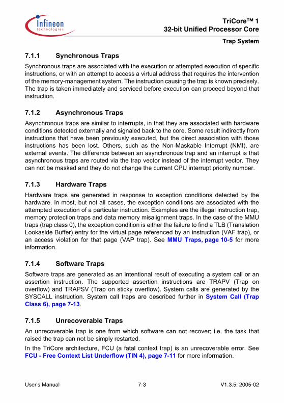
TriCore™ 132-bit Unified Processor Core
Trap System
7.1.1 Synchronous TrapsSynchronous traps are associated with the execution or attempted execution of specificinstructions, or with an attempt to access a virtual address that requires the interventionof the memory-management system. The instruction causing the trap is known precisely.The trap is taken immediately and serviced before execution can proceed beyond thatinstruction.
7.1.2 Asynchronous TrapsAsynchronous traps are similar to interrupts, in that they are associated with hardwareconditions detected externally and signaled back to the core. Some result indirectly frominstructions that have been previously executed, but the direct association with thoseinstructions has been lost. Others, such as the Non-Maskable Interrupt (NMI), areexternal events. The difference between an asynchronous trap and an interrupt is thatasynchronous traps are routed via the trap vector instead of the interrupt vector. Theycan not be masked and they do not change the current CPU interrupt priority number.
7.1.3 Hardware TrapsHardware traps are generated in response to exception conditions detected by thehardware. In most, but not all cases, the exception conditions are associated with theattempted execution of a particular instruction. Examples are the illegal instruction trap,memory protection traps and data memory misalignment traps. In the case of the MMUtraps (trap class 0), the exception condition is either the failure to find a TLB (TranslationLookaside Buffer) entry for the virtual page referenced by an instruction (VAF trap), oran access violation for that page (VAP trap). See MMU Traps, page 10-5 for moreinformation.
7.1.4 Software TrapsSoftware traps are generated as an intentional result of executing a system call or anassertion instruction. The supported assertion instructions are TRAPV (Trap onoverflow) and TRAPSV (Trap on sticky overflow). System calls are generated by theSYSCALL instruction. System call traps are described further in System Call (TrapClass 6), page 7-13.
7.1.5 Unrecoverable TrapsAn unrecoverable trap is one from which software can not recover; i.e. the task thatraised the trap can not be simply restarted.In the TriCore architecture, FCU (a fatal context trap) is an unrecoverable error. SeeFCU - Free Context List Underflow (TIN 4), page 7-11 for more information.
User’s Manual 7-3 V1.3.5, 2005-02

TriCore™ 132-bit Unified Processor Core
Trap System
7.2 Trap HandlingThe actions taken on traps by the trap handling mechanisms are slightly different fromthose taken on external or software interrupts. A trap does not change the CPU interruptpriority, so the ICR.CCPN field is not updated. See Exception Priorities, page 7-14.
7.2.1 Trap Vector FormatThe trap handler vectors are stored in code memory in the trap vector table. The BTVregister specifies the Base address of the Trap Vector table. The vectors are made upof a number of short code segments, evenly spaced by eight words.If a trap handler is very short it may fit entirely within the eight words available in thevector code segment. If it does not fit the vector code segment then it should containsome initial instructions, followed by a jump to the rest of the handler.
7.2.2 Accessing the Trap Vector TableWhen a trap occurs, a trap identifier is generated by hardware. The trap identifier hastwo components:• The Trap Class Number (TCN) used to index into the trap vector table.• The Trap Identification Number (TIN) which is loaded into the data register D[15].The Trap Class Number is left shifted by five bits and ORd with the address in the BTVregister to generate the entry address of the trap handler.
7.2.3 Return Address (RA)The return address is saved in the return address register A[11].For a synchronous trap, the return address is the PC of the instruction that caused thetrap. Only the SYS trap and FCD trap are different. On a SYS trap, triggered by theSYSCALL instruction, the return address points to the instruction immediately followingSYSCALL. The behaviour for the FCD trap is described in FCD - Free Context listDepletion (TIN 1), page 7-10.For an asynchronous trap, the return address is that of the instruction that would havebeen executed next, if the asynchronous trap had not been taken. The return addressfor an interrupt follows the same rule.
User’s Manual 7-4 V1.3.5, 2005-02

TriCore™ 132-bit Unified Processor Core
Trap System
7.2.4 Trap Vector TableThe entry-points of all Trap Service Routines are stored in memory in the Trap VectorTable. The BTV register specifies the base address of the Trap Vector Table in memory.It can be assigned to any available code memory. The BTV register can be modifiedusing the MTCR instruction during the initialization phase of the system, (the BTVregister is ENDINIT protected). This arrangement makes it possible to have multipleTrap Vector Tables and switch between them by changing the contents of the BTVregister.When a trap event occurs, a trap identifier is generated by the hardware detecting theevent. The trap identifier is made up of a Trap Class Number (TCN) and a TrapIdentification Number (TIN).The TCN is left-shifted by five bits and ORd with the address in the BTV register to formthe entry address of the TSR. Because of this operation, it is recommended that bits [7:5]of register BTV are set to 0 (see Figure 27). Note that bit 0 of the BTV register is always0 and can not be written to (instructions have to be aligned on even byte boundaries).Left-shifting the TCN by 5 bits creates entries into the Trap Vector Table which areevenly spaced 8 words apart. If a trap handler (TSR) is very short, it may fit entirely withinthe eight words available in the Trap Vector Table entry. Otherwise, the code at the entrypoint must ultimately cause a jump to the rest of the TSR residing elsewhere in memory.Unlike the Interrupt Vector Table, entries in the Trap Vector Table cannot be spanned.
Figure 27 Trap Vector Table Entry Address Calculation
User’s Manual 7-5 V1.3.5, 2005-02

TriCore™ 132-bit Unified Processor Core
Trap System
7.2.5 Initial State upon a TrapThe initial state when a trap occurs is defined as follows:• The upper context is saved.• The return address in A[11] is updated.• The TIN is loaded into D[15].• The stack pointer in A[10] is set to the Interrupt Stack Pointer (ISP) when the
processor was not previously using the interrupt stack (in case of PSW.IS = 0). Thestack pointer bit is set for using the interrupt stack: PSW.IS = 1.
• The I/O mode is set to Supervisor mode, which means all permissions are enabled:PSW.IO = 10B.
• The current Protection Register Set is set to 0: PSW.PRS = 00B.• The Call Depth Counter (CDC) is cleared, and the call depth limit is set for 64:
PSW.CDC = 0000000B.• Call Depth Counter is enabled, PSW.CDE = 1.• Write permission to global registers A[0], A[1], A[8], A[9] is disabled: PSW.GW = 0.• The interrupt system is globally disabled: ICR.IE = 0. The ‘old’ ICR.IE and ICR.CCPN
are saved into PCXI.PIE and PCXI.PCPN respectively. ICR.CCPN remainsunchanged.
• The trap vector table is accessed to fetch the first instruction of the trap handler.Although traps leave the ICR.CCPN unchanged, their handlers still begin execution withinterrupts disabled. They can therefore perform critical initial operations withoutinterruptions, until they specifically re-enable interrupts.For the non-recoverable FCU trap, the initial state is different. The upper context cannotbe saved. Only the following states are guaranteed:• The TIN is loaded into D[15].• The stack pointer in A[10] is set to the Interrupt Stack Pointer (ISP) when the
processor was not previously using the interrupt stack (in case of PSW.IS == 0).• The I/O mode is set to Supervisor mode (all permissions are enabled:
PSW.IO = 10B).• The current Protection Register Set is set to 0: PSW.PRS = 00B.• The interrupt system is globally disabled: ICR.IE = 0. ICR.CCPN remains
unchanged.• The trap vector table is accessed to fetch the first instruction of the FCU trap handler.
User’s Manual 7-6 V1.3.5, 2005-02

TriCore™ 132-bit Unified Processor Core
Trap System
7.3 Trap DescriptionsThe following sub-sections describe the trap classes and specific traps listed in Table 9Supported Traps, page 7-1.
7.3.1 MMU Traps (Trap Class 0)For those implementations that include a Memory Management Unit (MMU), Trapclass 0 is reserved for MMU traps. There are two traps within this class, VAF and VAP.
VAF - Virtual Address Fill (TIN 0)The VAF trap is generated when the MMU is enabled and the virtual address referencedby an instruction does not have a page entry in the MMU Translation Lookaside Buffer(TLB).
VAP - Virtual Address Protection (TIN 1)The VAP trap is generated (when the MMU is enabled) by a memory access undergoingPTE translation that is not permitted by the PTE protection settings, or by a User-0 modeaccess to an upper segment that does not have the privileged peripheral property.
7.3.2 Internal Protection Traps (Trap Class 1)Trap class 1 is for traps related to the internal protection system. The memory protectiontraps in this class, MPR, MPW, and MPX, are for the range-based protection system andare independent of the page-based VAP protection trap of trap class 0. See MemoryProtection System, page 9-1 for more details.All memory protection traps (MPR, MPW, MPX, MPP, and MPN), are based on thevirtual addresses that undergo direct translation.The following internal Protection Traps are defined:
PRIV - Privilege Violation (TIN 1)A program executing in one of the User modes (User-0 or User-1 mode) attempted toexecute an instruction not allowed by that mode.A table of instructions which are restricted to Supervisor mode or User-1 mode, issupplied in the Instruction Set chapter of Volume 2 of this manual.
MPR - Memory Protection Read (TIN 2)The MPR trap is generated when the memory protection system is enabled and theeffective address of a load, LDMST or SWAP instruction does not lie within any rangewith read permissions enabled. This trap is not generated when an access violationoccurs during a context save/restore operation.
User’s Manual 7-7 V1.3.5, 2005-02

TriCore™ 132-bit Unified Processor Core
Trap System
MPW - Memory Protection Write (TIN 3)The MPW trap is generated when the memory protection system is enabled and theeffective address of a store, LDMST or SWAP instruction does not lie within any rangewith write permissions enabled.This trap is not generated when an access violation occurs during a context save/restoreoperation.
MPX - Memory Protection Execute (TIN 4)The MPX trap is generated when the memory protection system is enabled and the PCdoes not lie within any range with execute permissions enabled.
MPP - Memory Protection Peripheral Access (TIN 5)A program executing in User-0 mode attempted a load or store access to a segment thathas the privileged peripheral property. See Physical Memory Attributes(PMA), page 8-1.
MPN - Memory Protection Null address (TIN 6)The MPN trap is generated whenever any program attempts a load / store operation toeffective address zero.
GRWP - Global Register Write Protection (TIN 7)A program attempted to modify one of the global address registers (A[0], A[1], A[8] orA[9]) when it did not have permission to do so.
7.3.3 Instruction Errors (Trap Class 2)Trap class 2 is for signalling various types of instruction errors. Instruction errors includeerrors in the instruction opcode, in the instruction operand encodings, or for memoryaccesses, in the operand address.
IOPC - Illegal Opcode (TIN 1)An invalid instruction opcode was encountered. An invalid opcode is one that does notcorrespond to any instruction known to the implementation.
UOPC - Unimplemented Opcode (TIN 2)An unimplemented opcode was encountered. An unimplemented opcode correspondsto a known instruction that is not implemented in a given hardware implementation. Theinstruction may be implemented via software emulation in the trap handler.
User’s Manual 7-8 V1.3.5, 2005-02

TriCore™ 132-bit Unified Processor Core
Trap System
Example UOPC conditions are:• A MMU instruction if the MMU is not present.• A FPU instruction if the FPU is not present.• An external coprocessor instruction if the external coprocessor is not present.
OPD - Invalid Operand (TIN 3)The OPD trap may be raised for instructions that take an even-odd register pair as anoperand, if the operand specifier is odd. The OPD trap may also be raised for other caseswhere operands are invalid.Implementations are not architecturally required to raise this trap, and may treat invalidoperands in an implementation defined manner.
ALN - Data Address Alignment (TIN 4)An ALN trap is raised when the address for a data memory operation does not conformto the required alignment rules. See Alignment Requirements, page 3-4, for moreinformation on these rules.
MEM - Invalid Memory Address (TIN 5)The MEM trap is raised when the address of an access can be determined to eitherviolate an architectural constraint or an implementation constraint.Defined MEM trap subclasses are different segment, segment crossing, CSFR access,CSA restriction and scratch range.An implementation must define which implementation contraint MEM traps it will raise,or the alternative behaviour if the MEM trap is not raised. It must also document anyother implementation specific MEM traps it will raise.Architectural contraints which will raise the MEM trap are:• An addressing mode that adds an offset to a base address results in an effective
address that is in a different segment to the base address (different segment).• A data element is accessed with an address, such that the data object spans the end
of one segment and the beginning of another segment (segment crossing)Implementation contraints which can raise the MEM trap are• A memory address is used to access a Core SFR (CSFR) rather than using a
MTCR/MFCR instruction (CSFR access)• A memory address is used for a CSA access and it is not valid for the implementation
to place CSA there (CSA restriction)An access to Scratch memory is attempted using a memory address which lies outsidethe implemented region of memory (scratch range error).
User’s Manual 7-9 V1.3.5, 2005-02

TriCore™ 132-bit Unified Processor Core
Trap System
7.3.4 Context Management (Trap Class 3)Trap class 3 is for exception conditions detected by the context management subsystem,in the course of performing (or attempting to perform) context save and restoreoperations connected to function calls, interrupts, traps, and returns.
FCD - Free Context list Depletion (TIN 1)The FCD trap is generated after a context save operation, when the operation causesthe free context list to become ‘almost empty’. The ‘almost empty’ condition is signaledwhen the CSA used for the save operation is the one pointed to by the context list limitregister LCX. The operation responsible for the context save completes normally andthen the FCD trap is taken.If the operation responsible for the context save was the hardware interrupt or trap entrysequence, then the FCD trap handler will be entered before the first instruction of theoriginal interrupt or trap handler is executed. The return address for the FCD trap willpoint to the first instruction of the interrupt or trap handler.The FCD trap handler is normally expected to take some form of action to rectify thecontext list depletion. The nature of that action is OS dependent, but the general choicesare to allocate additional memory for CSA storage, or to terminate one or more tasks,and return the CSAs on their call chains to the free list. A third possibility is not toterminate any tasks outright, but to copy the call chains for one or more inactive tasks touncached external or secondary memory that would not be directly usable for CSAstorage, and release the copied CSAs to the free list. In that instance the OS taskscheduler would need to recognize that the inactive task's call chain was not resident inCSA storage, and restore it before dispatching the task.The FCD trap itself uses one additional CSA beyond the one designated by the LCXregister, so LCX must not point to the actual last entry on the free context list. In addition,it is possible that an asynchronous trap condition, such as an external bus error, will bereported after the FCD trap has been taken, interrupting the FCD trap handler and usingone more CSA. Therefore, to avoid the possibility of a context list underflow, the freecontext list must include a minimum of two CSAs beyond the one pointed to by the LCXregister. If the FCD trap handler makes any calls, then additional CSA reserves areneeded.In order to allow the trap handlers for asynchronous traps to recognize when they haveinterrupted the FCD trap handler, the FCDSF flag in the SYSCON (system configuration)register is set whenever an FCD trap is generated. The FCDSF bit should be tested bythe handler for any asynchronous trap that could be taken while an FCD trap is beinghandled. If the bit is found to be set, the asynchronous trap handler must avoid makingany calls, but should queue itself in some manner that allows the OS to recognize thatthe trap occurred. It should then carry out an immediate return, back to the interruptedFCD trap handler. See System Control Registers (SYSCON), page 4-27.
User’s Manual 7-10 V1.3.5, 2005-02
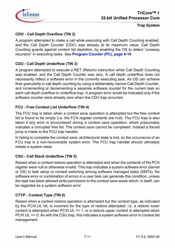
TriCore™ 132-bit Unified Processor Core
Trap System
CDO - Call Depth Overflow (TIN 2)A program attempted to make a call while executing with Call Depth Counting enabled,and the Call Depth Counter (CDC) was already at its maximum value. Call DepthCounting guards against context list depletion, by enabling the OS to detect ‘runawayrecursion’ in executing tasks. See Program Counter (PC), page 4-10.
CDU - Call Depth Underflow (TIN 3)A program attempted to execute a RET (Return) instruction while Call Depth Countingwas enabled, and the Call Depth Counter was zero. A call depth underflow does notnecessarily reflect a software error in the currently executing task. An OS can achievefiner granularity in call depth counting by using a deliberately narrow Call Depth Counter,and incrementing or decrementing a separate software counter for the current task oneach call depth overflow or underflow trap. A program error would be indicated only if thesoftware counter were already zero when the CDU trap occurred.
FCU - Free Context List Underflow (TIN 4)The FCU trap is taken when a context save operation is attempted but the free contextlist is found to be empty (i.e. the FCX register contents are null). The FCU trap is alsotaken if any error is encountered during a context save operation, which presumablyindicates a corrupted free list. The context save cannot be completed. Instead a forcedjump is made to the FCU trap handler.In failing to complete the context save, architectural state is lost, so the occurrence of anFCU trap is a non-recoverable system error. The FCU trap handler should ultimatelyinitiate a system reset.
CSU - Call Stack Underflow (TIN 5)Raised when a context restore operation is attempted and when the contents of the PCXregister were null or otherwise invalid. This trap indicates a system software error (kernelor OS) in task setup or context switching among software managed tasks (SMTs). Nosoftware error or combination of errors in a user task can generate this condition, unlessthe task has been allowed write permission to the context save areas which, in itself, canbe regarded as a system software error.
CTYP - Context Type (TIN 6)Raised when a context restore operation is attempted but the context type, as indicatedby the PCXI.UL bit, is incorrect for the type of restore attempted; i.e. a restore lowercontext is attempted when PCXI.UL == 1, or a restore upper context is attempted whenPCXI.UL == 0. As with the CSU trap, this indicates a system software error in context listmanagement.
User’s Manual 7-11 V1.3.5, 2005-02

TriCore™ 132-bit Unified Processor Core
Trap System
NEST - Nesting Error (TIN 7)An RFE (Return From Exception) instruction was attempted when the Call DepthCounter was non-zero. The return from an interrupt or trap handler should normallyoccur within the body of the interrupt or trap handler itself, or in code to which the handlerhas branched, rather than code called from the handler. If this is not the case there willbe one or more saved contexts on the residual call chain that must be popped andreturned to the free list, before the RFE can be legitimately issued.
7.3.5 System Bus and Peripheral Errors (Trap Class 4)
PSE - Program Fetch Synchronous Error (TIN 1)The PSE trap is raised when:• A bus error1) occurred because of an instruction fetch.• An instruction fetch targets a segment that does not have the code fetch property.
See Physical Memory Attributes (PMA), page 8-1.• A code fetch operation from Program scratchpad RAM (PSPR) (See Scratchpad
RAM, page 8-4) where the access is beyond the end of the memory range.
DSE - Data Access Synchronous Error (TIN 2)The DSE trap is raised when:• A data access is attempted to a segment that does not have the data access
property. (See Physical Memory Attributes (PMA), page 8-1).• Whenever a bus error occurred because of a data load operation. It is also raised in
the case of a data load operation from Data scratchpad RAM (DSPR) (ScratchpadRAM, page 8-4) where the access is beyond the end of the memory range.
Note: There are implementation-dependent registers for DSE which can be interrogatedto determine the source of the error more precisely. Refer to the User's Manual fora specific TriCore implementation for more details.
DAE - Data Access Asynchronous Error (TIN 3)The DAE trap is raised when the memory system reports back an error which cannotimmediately be linked to a currently executing instruction. Generally this means an errorreturned on the system bus from a peripheral or external memory.This trap is raised whenever a bus error occurred because of a data store operation, orwhen:
1) A bus fetch error is also generated for an instruction fetch to the data scratch pad RAM region (D000 0000Hto D3FF FFFFH) when the memory access is outside the range of the actual scratchpad RAMs.
User’s Manual 7-12 V1.3.5, 2005-02

TriCore™ 132-bit Unified Processor Core
Trap System
• There is a data store operation to local scratch memory but the access is beyond theend of the memory range.
• There is an error caused by a cache management instruction.Note: There are implementation-dependent registers for DAE which can be interrogated
to determine the source of the error more precisely. Refer to the User's Manual fora specific TriCore implementation for more details.
7.3.6 Assertion Traps (Trap Class 5)
OVF - Arithmetic Overflow (TIN 1)Raised by the TRAPV instruction, if the overflow bit in the PSW is set (PSW.V == 1).
SOVF - Sticky Arithmetic Overflow (TIN 2)Raised by the TRAPSV instruction, if the sticky overflow bit in the PSW is set(PSW.SV == 1).
7.3.7 System Call (Trap Class 6)
SYS - System Call (TIN = 8-bit unsigned immediate constant in SYSCALL)The SYS trap is raised immediately after the execution of the SYSCALL instruction, toinitiate a system call. The TIN that is loaded into D[15] when the trap is taken is not fixed,but is specified as an 8-bit unsigned immediate constant in the SYSCALL instruction.The return address points to the instruction immediately following the SYSCALL.
7.3.8 Non-Maskable Interrupt (Trap Class 7)
NMI - Non-Maskable Interrupt (TIN 0)The causes for raising a Non-Maskable Interrupt are implementation dependent.Typically there is an external pin that can be used to signal the NMI, but it may also beraised in response to such things as a watchdog timer interrupt, or an impending powerfailure. Refer to the User's Manual for a specific TriCore implementation for more details.
7.3.9 Debug Traps
BBM - Break Before Make / BAM - Break After MakePlease refer to the Core Debug Controller chapter for information on debug traps. SeeChapter 11 Core Debug Controller (CDC), page 11-1.
User’s Manual 7-13 V1.3.5, 2005-02

TriCore™ 132-bit Unified Processor Core
Trap System
7.4 Exception PrioritiesThe priority order between an asynchronous trap, a synchronous trap, and an interruptfrom the software architecture model, is as follows:1. Asynchronous trap (highest priority).2. Synchronous trap.3. Interrupt (lowest priority).The following trap rules must also be considered:1. The older the instruction in the instruction sequence which caused the trap, the
higher the priority of the trap. All potential traps with lower priorities are void.2. Attempting to save a context with an empty free context list (FCX = 0) results in a
FCU (Free Context List Underflow) trap. This trap takes priority over all otherexceptions.
3. When the same instruction causes several synchronous traps anywhere in thepipeline, priorities follow those shown in the table below.
Table 10 Synchronous Trap PrioritiesPriority Type of TrapInstruction Fetch Traps1 Breakpoint (Virtual address, BBM)2 VAF-P3 VAP-P4 MPX5 PSEInstruction Format Traps6 IOPC7 OPD8 UOPCInstruction Traps9 Breakpoint trap (Instruction, BBM)10 PRIV11 GRWP12 SYSContext Traps13 FCD14 FCU (Synchronous)
User’s Manual 7-14 V1.3.5, 2005-02

TriCore™ 132-bit Unified Processor Core
Trap System
15 CSU16 CDO17 CDU18 NEST19 CTYPData Memory Access Traps20 MEM (Data address)21 ALN22 MPN23 VAF-D24 VAP-D25 MPR26 MPW27 MPP28 DSEGeneral Data Traps29 SOVF30 OVF31 Breakpoint trap (BAM)
Table 11 Asynchronous Trap PrioritiesPriority Asynchronous Traps1 NMI2 DAE1)
1) DAE is used for both load and store errors.
Table 10 Synchronous Trap Priorities (Continued)
User’s Manual 7-15 V1.3.5, 2005-02

TriCore™ 132-bit Unified Processor Core
Trap System
User’s Manual 7-16 V1.3.5, 2005-02

TriCore™ 132-bit Unified Processor Core
Physical Memory Attributes (PMA)
8 Physical Memory Attributes (PMA)This chapter describes the Physical Memory Attributes (PMA) that regions of theTriCore™ physical address map may or may not have. These attributes are defined bygroups of physical memory properties.
8.1 Physical Memory Properties (PMP)The TriCore architecture defines properties which physical memory addresses may ormay not possess. These properties are:• Privileged Peripheral (P).• Cacheable (C).• Speculative (S).• Code Fetch (F).• Data Access (D).Each property defines a characteristic of the accesses that are possible to a physicalmemory region. For example, an address that does not have the cacheable property C,would be described as Non-cacheable C.In the following definitions the concept of necessary and speculative accesses isintroduced. Necessary accesses are those required to correctly compute the programand any implementation or simulation of the program execution must perform theseaccesses. Speculative accesses are those that an implementation may make in order toimprove performance either in correct or incorrect anticipation of a necessary access.
Privileged Peripheral (P)Only Supervisor and User-1 mode data accesses are possible. No User-0 mode dataaccess is possible. User-0 mode data accesses result in an MPP (Memory ProtectionPeripheral access) trap. All accesses are exempt from the protection system settings.PTE translation where the physical address targets a region with this property results inundefined behaviour.
Cacheable (C)It is possible for data and code fetch accesses to the region to be cached by the CPU ifa data cache or code cache is respectively present and enabled.
Speculative (S)It is possible to perform speculative data accesses to the memory. A speculative dataaccess is a read access to memory addresses that are not strictly necessary for correctprogram execution. The processor never performs speculative write accesses which arevisible in a memory region.
User’s Manual 8-1 V1.3.5, 2005-02

TriCore™ 132-bit Unified Processor Core
Physical Memory Attributes (PMA)
Code Fetch (F)Fetch accesses are possible to this region. The fetch property allows full speculation onall fetch accesses to the region. The cacheable property has no affect on the amount orrange of speculation of code fetches. If a necessary fetch access is directed by programflow to a physical memory region that does not have the fetch property then a PSE(Program fetch Synchronous Error) trap occurs.
Data Access (D)Data accesses are possible to this region. If a data access is directed by necessaryprogram flow to a physical memory region that does not have the Data Access property,then a DSE (Data access Synchronous Error) trap occurs.For data accesses, the interpretation of the combinations of the Privileged Peripheral,Cacheable and Speculative properties for a memory region are defined in Table 12. Allother combinations of these three properties not present in this table, are reserved.
Table 12 Data Access - Cacheable and Speculative PropertiesName Privileged
Peripheral Property
Cacheable Property
Speculative Property
Behaviour of Physical Memory Region
Precise data access
P or P C S The processor only performs necessary accesses, in order, to the region.
Non-Cached access
P C S The processor may read an entire cache line1) containing the address of a necessary access and place it in a buffer for subsequent accesses. The order of accesses is not guaranteed 2).
1) The size of a cache line is implementation dependant. Examples of implemented cache lines are 16-bytes and32-bytes, but may be smaller or larger.
2) The order of non-cached data accesses can be guaranteed by inserting a DSYNC instruction (ref to DSYNC)after each load or store instruction.
Full Speculation
P C S The processor may perform speculative read accesses to entire cache lines in physical memory and place them in the cache. The order of accesses is not guaranteed.
User’s Manual 8-2 V1.3.5, 2005-02

TriCore™ 132-bit Unified Processor Core
Physical Memory Attributes (PMA)
8.2 Physical Memory Attributes (PMA)A physical memory attribute is a defined set of physical memory properties. Thearchitecture defines four attributes:Peripheral Space = PCSFD.Emulator Space = PCSFD.Cacheable Memory = PCSFD.Non-Cacheable Memory = PCSFD.All accesses to physical memory that has the Emulator Space attribute are directlytranslated (See Memory Management Unit (MMU), page 10-1) and are not subject tothe protection constraints imposed by the protection system (See Memory ProtectionSystem, page 9-1); i.e. It is not possible to generate an MPX, MPR or MPW trap with amemory access to Emulator Space.
8.2.1 Physical Memory Attributes of the Address MapThe TriCore 4 GBytes (32-bit) of physical address space is divided into 16 equally sizedsegments. Each segment has its own physical memory attribute.Segment FH is constrained to be Peripheral Space and the lower 15 segments haveimplementation defined physical memory attributes, although Segment DH isconstrained to be either Cacheable or Non-Cacheable Memory. The standardimplementation attributes are shown in the following table:
Table 13 TriCore Default Physical Memory Attributes for all Segments Segment AttributesFH
1)
1) FH is constrained to be Peripheral Space.
Peripheral Space.EH Peripheral Space.DH
2)
2) See Data Scratchpad Register (DSPR), page 6-2.
Non-cacheable Memory.CH Cacheable Memory.BH Non-cacheable Memory.AH Non-cacheable Memory.9H Cacheable Memory.8H Cacheable Memory.7H - 0H Cacheable Memory.
User’s Manual 8-3 V1.3.5, 2005-02

TriCore™ 132-bit Unified Processor Core
Physical Memory Attributes (PMA)
The Emulator Space attribute is assigned to an implementation defined region ofmemory when the Debug Mode is enabled.All physical memory accesses are subject to the constraints imposed by the PMAattributes before being permitted to execute.
8.3 Scratchpad RAMSegment D contains the scratchpad RAM. There are two different scratchpad RAMs:• DSPR - Data scratchpad RAM.• PSPR - Program scratchpad RAM.
Table 14 Scratchpad RAMSegment D Regions PropertiesDFFFFFFFH – D8000000H Implementation DependentD7FFFFFFH – D4000000H PSPRD3FFFFFFH – D0000000H DSPR
User’s Manual 8-4 V1.3.5, 2005-02

TriCore™ 132-bit Unified Processor Core
Physical Memory Attributes (PMA)
8.4 Permitted versus Valid AccessesA memory access can be permitted without necessarily being valid. There are threesources of permission for a memory access, the Protection System (PS), the MemoryManagement Unit (MMU) and the Physical Memory Attributes (PMA). If a memoryaccess is permitted by the MMU or PS, then it must also be permitted by the PMA for theaccess to proceed, as shown in Figure 28. A memory access is not valid if the addressof the access is to an unimplemented region of memory or is misaligned; therefore anaccess can be permitted but not valid.
Figure 28 Translation Paths
The PS and MMU act upon the direct translation and virtual translation pathsrespectively, therefore the permission for a memory access that undergoes virtualtranslation lies only with the MMU, not the PS, and vice-versa.
User’s Manual 8-5 V1.3.5, 2005-02

TriCore™ 132-bit Unified Processor Core
Physical Memory Attributes (PMA)
User’s Manual 8-6 V1.3.5, 2005-02

TriCore™ 132-bit Unified Processor Core
Memory Protection System
9 Memory Protection SystemThe TriCore™ protection system provides the essential features needed to isolate errorsand facilitate debugging. The system is unobtrusive, imposing little overhead and avoidsnon-deterministic run-time behaviour.The protection system incorporates hardware mechanisms that protect user-specifiedmemory ranges from unauthorized read, write, or instruction fetch accesses. Theprotection hardware can in addition, be used to generate signals to the Core DebugController (CDC) (See Core Debug Controller (CDC), page 11-1).This chapter describes the hardware operation of the protection system and introducesthe use of the protection features by software in real-time systems. The protectionsystem differentiates between peripheral protection and memory protection. Themajority of this chapter is concerned with memory protection, which does not apply tomemory regions that have the peripheral space or emulator space attribute. See thechapter Physical Memory Attributes (PMA), page 8-1.Effective addresses are translated into physical addresses using one of two translationmechanisms:• Direct translation.• Page Table Entry (PTE) based translation.These translation mechanisms are both defined in the chapter Memory ManagementUnit (MMU), page 10-1.Memory protection for addresses that undergo direct address translation is enforcedusing the range-based memory protection system described in this chapter.
9.1 Memory Protection RegistersTriCore contains register sets that specify the address range and the accesspermissions for a number of memory ranges. The PSW.PRS field is used to select whichregister set is active at a given time. Two register sets are selected simultaneously:• One Data Memory Protection.• One Code Memory Protection.The PSW.PRS field allows selection of up to four such register sets; four for data andfour for code. See Program Status Word (PSW), page 4-11 for more details on thePSW.
User’s Manual 9-1 V1.3.5, 2005-02

TriCore™ 132-bit Unified Processor Core
Memory Protection System
Figure 29 Memory Protection Register Sets
The number of register sets provided for memory protection is specific to each TriCoreimplementation, limited to a minimum of two and a maximum of four. This document onlydescribes the generic format of these register sets. Unimplemented register setaddresses are reserved and undefined.Each register set is made up of several range registers (also called Range TableEntries). The number of range registers in a Data or Code Memory Protection Set isimplementation defined. Each Range Table Entry (Figure 30, page 9-3) consists of aSegment Protection register pair and a bit field within a common Mode register.The register pair specifies the lower and upper boundary addresses of the memoryrange.Lower Bound <= address < Upper Bound.The Mode register contains the access permission and debug control bits. The controloptions are different for the data and the code memory protection.For load and store operations, data address values are checked against the entries inthe data range table.On instruction fetches, the PC value for the fetch is checked against the entries in thecode range table. When an address is found to fall outside of all ranges defined in theappropriate range table, then permission for the access is denied. When an address isfound to fall within a range defined in the appropriate range table, the associated modetable entry is checked for access permissions. An instruction fetch cannot occur from abyte aligned address, and so the least significant bit of the Code Segment Protectionupper and lower bound registers (CPRx_n) is not writeable and always returns zero.
User’s Manual 9-2 V1.3.5, 2005-02

TriCore™ 132-bit Unified Processor Core
Memory Protection System
Figure 30 Example of Four Range Table Entries in a Protection Register Set
User’s Manual 9-3 V1.3.5, 2005-02

TriCore™ 132-bit Unified Processor Core
Memory Protection System
9.1.1 Memory Protection Registers I
DPRx_nUData Segment Protection Register x_n Upper Bound (x = set number 0 to 3; n = range number) Reset Value: Implementation Specific
31 30 29 28 27 26 25 24 23 22 21 20 19 18 17 16
UPPBND
rw
15 14 13 12 11 10 9 8 7 6 5 4 3 2 1 0
UPPBND
rw
Field Bits Type DescriptionUPPBND [31:0] rw DPRx_n Upper Boundary Address
DPRx_nLData Segment Protection Register x_n Lower Bound(x = set number 0 to 3; n = range number) Reset Value: Implementation Specific
31 30 29 28 27 26 25 24 23 22 21 20 19 18 17 16
LOWBND
rw
15 14 13 12 11 10 9 8 7 6 5 4 3 2 1 0
LOWBND
rw
Field Bits Type DescriptionLOWBND [31:0] rw DPRx_n Lower Boundary Address
User’s Manual 9-4 V1.3.5, 2005-02

TriCore™ 132-bit Unified Processor Core
Memory Protection System
CPRx_nUCode Segment Protection Register x_n Upper Bound (x = set number 0 to 3; n = range number) Reset Value: Implementation Specific
31 30 29 28 27 26 25 24 23 22 21 20 19 18 17 16
UPPBND
rw
15 14 13 12 11 10 9 8 7 6 5 4 3 2 1 0
UPPBND 0
rw r
Field Bits Type DescriptionUPPBND [31:0] rw CPRx_n Upper Boundary Address
The least significant bit is not writeable and always returns zero.
CPRx_nLCode Segment Protection Register x_n Lower Bound (x = set number 0 to 3; n = range number) Reset Value: Implementation Specific
31 30 29 28 27 26 25 24 23 22 21 20 19 18 17 16
LOWBND
rw
15 14 13 12 11 10 9 8 7 6 5 4 3 2 1 0
LOWBND 0
rw r
Field Bits Type DescriptionLOWBND [31:0] rw CPRx_n Lower Boundary Address
The least significant bit is not writeable and always returns zero.
User’s Manual 9-5 V1.3.5, 2005-02

TriCore™ 132-bit Unified Processor Core
Memory Protection System
DPMx Data Protection Mode Register x (x = set number 0 to 3) Reset Value: Implementation Specific
31 30 29 28 27 26 25 24 23 22 21 20 19 18 17 16
WE3 RE3 WS3 RS3 WBL3
RBL3
WBU3
RBU3 WE2 RE2 WS2 RS2 WB
L2RBL2
WBU2
RBU2
rw rw rw rw rw rw rw rw rw rw rw rw rw rw rw rw
15 14 13 12 11 10 9 8 7 6 5 4 3 2 1 0
WE1 RE1 WS1 RS1 WBL1
RBL1
WBU1
RBU1 WE0 RE0 WS0 RS0 WB
L0RBL0
WBU0
RBU0
rw rw rw rw rw rw rw rw rw rw rw rw rw rw rw rw
Field Bits Type DescriptionWE(3-0) 31, 23,
15, 7rw Address Field Write Enable
0 : Data write accesses to associated address range not permitted.
1 : Data write accesses to associated address range permitted.
RE(3-0) 30, 22, 14, 6
rw Address Field Read Enable0 : Data read accesses to associated address range not
permitted.1 : Data read accesses to associated address range
permitted.WS(3-0) 29, 21,
13, 5rw Address Range Data Write Signal
0 : Data write signal disabled.1 : Signal asserted to Core Debug Controller (CDC) on
data write accesses to associated address range.RS(3-0) 28, 20,
12, 4rw Address Range Data Read Signal
0 : Data read signal disabled.1 : Signal asserted to Core Debug Controller (CDC) on
data read accesses to associated address range.WBL(3-0) 27, 19,
11, 3rw Data Write Signal on Lower Bound Access
0 : Data write signal disabled.1 : Signal asserted to Core Debug Controller (CDC) on
data write access to an address that matches lower bound address of associated address range.
User’s Manual 9-6 V1.3.5, 2005-02

TriCore™ 132-bit Unified Processor Core
Memory Protection System
RBL(3-0) 26, 18, 10, 2
rw Data Read Signal on Lower Bound Access0 : Data read signal disabled.1 : Signal asserted to Core Debug Controller (CDC) on
data read access to an address that matches lower bound address of associated address range.
WBU(3-0) 25, 17, 9, 1
rw Data Write Signal on Upper Bound Access0 : Write signal disabled.1 : Signal asserted to Core Debug Controller (CDC) on
data write access to an address that matches upper bound address of associated address range.
RBU(3-0) 24, 16, 8, 0
rw Data Read Signal on Upper Bound Access0 : Data read signal disabled.1 : Signal asserted to Core Debug Controller (CDC) on
data read access to an address that matches upper bound address of associated address range.
Field Bits Type Description
User’s Manual 9-7 V1.3.5, 2005-02

TriCore™ 132-bit Unified Processor Core
Memory Protection System
CPMxCode Protection Mode Register x(x = set number 0 to 3) Reset Value: Implementation Specific
31 30 29 28 27 26 25 24 23 22 21 20 19 18 17 16
XE3 - XS3 - BL3 - BU3 XE2 - XS2 - BL2 - BU2
rw rw rw rw rw rw rw rw
15 14 13 12 11 10 9 8 7 6 5 4 3 2 1 0
XE1 - XS1 - BL1 - BU1 XE0 - XS0 - BL0 - BU0
rw rw rw rw rw rw rw rw
Field Bits Type DescriptionXE(3-0) 31, 23,
15, 7rw Address Range Execute Enable
0 : Instruction fetch accesses to associated address range not permitted.
1 : Instruction fetch accesses to associated address range permitted.
- 30, 28, [26:25],22, 20, [18:17],14, 12, [10:9], 6, 4, [2:1]
- Reserved Field
XS(3-0) 29, 21, 13, 5
rw Address Range Execute Signal0 : Execute signal disabled.1 : Signal asserted to Core Debug Controller (CDC) on
instruction fetch accesses to associated address range.
BL(3-0) 27, 19, 11, 3
rw Execute Signal on Lower Bound Access0 : Lower bound execute signal disabled.1 : Signal asserted to Core Debug Controller (CDC) on
instruction fetch access to an address that matches lower bound address of associated address range.
User’s Manual 9-8 V1.3.5, 2005-02

TriCore™ 132-bit Unified Processor Core
Memory Protection System
At any given time one of the sets is the current protection register set which determinesthe legality of memory accesses by the current task or ISR. The PRS field in the PSWdetermines the current protection register set number.
Modes of Use for Range Table EntriesIndividual range table entries can be used just for memory protection or for debugging.One entry is rarely used for both purposes. If the upper and lower bound values havebeen set for debug breakpoints they are probably not meaningful for defining protectionranges, and vice-versa. However, it is both possible and reasonable to have someentries used for memory protection and others used for debugging.To disable an entry for use in memory protection, clear both the RE and WE bits in a datarange table entry or clear the XE bit in a code range table entry. The entry can bedisabled for use in debugging by clearing any debug signal bits.When a range entry is being used for debugging, the debug signal bits that are setdetermine whether it is used as a single range comparator (giving an in-range/notin-range signal) or as a pair of equal comparators. The two uses are not mutuallyexclusive.
Using Protection Register SetsSupervisor mode does not automatically disable memory protection. The protectionregister set that is selected for Supervisor mode tasks will normally be set up to allowwrite access to regions of memory that are protected from User mode access. In additionSupervisor mode tasks can execute instructions to change the protection maps, or todisable the protection system entirely. But the Supervisor mode does not implicitlyoverride memory protection, and it is possible for a Supervisor mode task to take amemory protection trap.
BU(3-0) 24, 16, 8, 0
rw Execute Signal on Upper Bound Access0 : Upper bound execute signal disabled.1 : Signal asserted to Core Debug Controller (CDC) on
instruction fetch access to an address that matches upper bound address of associated address range.
Field Bits Type Description
User’s Manual 9-9 V1.3.5, 2005-02

TriCore™ 132-bit Unified Processor Core
Memory Protection System
9.2 Access Permissions for Intersecting Memory RangesThe permission to access a memory location is the OR of the memory rangepermissions. If one of the ranges allows it, the memory access is permitted. This meansthat when two ranges intersect, the intersecting regions will have the permission of themost permissive range.For example, if range A is set for read/write permission and range B read-only, theintersecting region of A and B will be read/write. Nesting of ranges can be used forexample to allow read/write access to a subrange of a larger range in which the currenttask is allowed read access.
9.2.1 ExampleFigure 31 illustrates the Data Protection Register Set x, where x is one of the four setsas selected by the PSW.PRS field. The register set in this example consists of four rangetable entries.
Figure 31 Example Configuration of a Data Protection Register Set
User’s Manual 9-10 V1.3.5, 2005-02

TriCore™ 132-bit Unified Processor Core
Memory Protection System
In Figure 31 the four Data Segment and four Data Protection Mode Registers are set upas follows:• Data Segment Protection Registers DPRx_3U and DPRx_3L, define the upper (U)
and lower (L) bound for Data Range 3. Data Protection Mode Register 3 (DPMx_3)defines the read-only permissions for Data Range 3.
• DPRx_2U and DPRx_2L define the upper (U) and lower (L) bound for Data Range 2.DPMx_2 defines the read-write permissions for Data Range 2.
Note: Data Range 2, which has read/write permission, is nested within Data Range 3,which has read-only permission. Because the intersecting rules state thatpermission to access a memory location is the OR of the regions permissions, thisregion therefore has read/write permission.
• DPRx_1U and DPRx_1L define the upper (U) and lower (L) bound for Data Range 1.DPMx_1 defines the permissions for Data Range 1.
• DPRx_0U and DPRx_0L define the upper (U) and lower (L) bound for Data Range 0.DPMx_0 defines the permissions for Data Range 0.
This same configuration can be used to illustrate Code Protection Register Set x.
User’s Manual 9-11 V1.3.5, 2005-02

TriCore™ 132-bit Unified Processor Core
Memory Protection System
9.3 Using the Memory Protection SystemWhen the protection system is enabled every memory access (read, write or execute) ischecked for legality before the access is performed. The legality is determined by all ofthe following:• The Protection Enable bit in the SYSCON register (SYSCON.PROTEN).• The currently selected protection register set (PSW.PRS).• The ranges defined in the protection register set.
9.3.1 Protection Enable bitFor the memory protection system to be active, the Protection Enable bit(SYSCON.PROTEN) must be set to one (SYSCON.PROTEN == 1). If the memoryprotection system is disabled (SYSCON.PROTEN == 0), then any access to anymemory address is permitted.
9.3.2 Set SelectionAt any given time, one of the sets is the current protection register set which determinesthe legality of memory accesses by the current task or Interrupt Service Routine. ThePSW.PRS field indicates the current Protection Register Set number.
9.3.3 Address RangeData addresses (read and write accesses) are checked against the currently selecteddata address range table, while instruction fetch addresses are checked against thecode address range tables. The mode entries for the data range table entries enable onlyread and write accesses, while the mode entries for the code range table entries enableonly execute access.In order for data to be read from program space, there must be an entry in the dataaddress range table that covers the address being read. Conversely there must be anentry in the code address range table that covers the instruction being read.The protection system does not differentiate between access permission levels. Thedata and code protection settings have the same effect, whether the permission level iscurrently set to Supervisor, User-1 or User-0 mode.The protection system does not apply to accesses in memory regions with the peripheralspace or emulator space attribute. If a memory access is attempted to either of thesesegments, the access is permitted by the protection system (but not necessarily thePhysical Memory Attributes) regardless of the protection system settings. For more onPMA, see Physical Memory Attributes (PMA), page 8-1.Saves or restores of contexts to the context save area (see Save and Restore ContextOperations, page 5-5) do not require the permission of the protection system toproceed.
User’s Manual 9-12 V1.3.5, 2005-02

TriCore™ 132-bit Unified Processor Core
Memory Protection System
9.3.4 TrapsThere are three traps generated by memory protection, each corresponding to the threeprotection mode register bits:• MPW (Memory Protection Write) trap = WE bit.• MPR (Memory Protection Read) trap = RE bit.• MPX (Memory Protection Execute) trap = XE bit.Refer to Chapter 7 Trap System, page 7-1 for a complete description of Traps.
9.4 Crossing Protection BoundariesA memory access can straddle two regions defined by the protection system. Figure 32shows a memory access (code or data) crossing the boundary of a permitted region anda ‘not permitted’ region of memory. In this situation it is implementation defined as towhether or not a memory protection trap is taken.To ensure deterministic behaviour in all implementations of TriCore, a region at leasttwice the size of the largest memory accesses, minus one byte, should be left as a bufferbetween each memory protection region.
Figure 32 Protection Boundaries
User’s Manual 9-13 V1.3.5, 2005-02

TriCore™ 132-bit Unified Processor Core
Memory Protection System
User’s Manual 9-14 V1.3.5, 2005-02

TriCore™ 132-bit Unified Processor Core
Memory Management Unit (MMU)
10 Memory Management Unit (MMU)This chapter describes the TriCore™ Memory Management Unit (MMU) architecture.The MMU is an optional component in TriCore configurations. It need not be present inevery system that uses the core, and even when present it can be disabled.If the MMU is not present and enabled in a system, then virtual memory and page-basedmemory access protection are not supported for that system. The range-basedprotection system (a non-optional core component) still provides basic memoryprotection services. For more details see Memory Protection System, page 9-1.The memory management features include:• 4 GBytes of virtual address space divided into 16 segments of 256 MBytes each. The
upper half of the virtual address space (segments [8H - FH]) is global, and mappeddirectly onto the physical address space. The lower segment (segments [0H - 7H]) isimplicitly qualified by an Address Space Identifier (ASI). The operating system canallocate distinct address spaces to each unique ASI. Two or more processes can alsoshare an address space ID, either serially or in parallel.
• 4 GBytes of physical address space divided into 16, 256 MByte segments.• Virtual to physical address translation by direct translation or via Page Table Entries
(PTE), depending on the segment number of the virtual address and the status of theMMU.
• Cacheability and access permissions based on physical memory attributes fordirectly translated addresses, or by a combination of physical memory attributes andvirtual page attributes for addresses translated via Page Table Entries. Attributes forsegments [8H - FH] are pre-defined in a system memory map.
Virtual addresses are always translated into physical addresses before accessingmemory. The virtual address is translated into a physical address using either directtranslation or Page Table Entry (PTE) translation.• Direct translation: If the virtual address belongs to the upper segment of the virtual
address space then the virtual address is directly used as the physical address. If thevirtual address belongs to the lower segment of the address space, then the virtualaddress is used directly as the physical address if the processor is operating inPhysical mode (i.e. the MMU is disabled or not present).
• PTE translation: If the virtual address belongs to the lower segment of the addressspace and the processor is operating in Virtual mode (i.e. the MMU is present andenabled), then the virtual address is translated using a Page Table Entry.
PTE translation is performed by replacing the Virtual Page Number (VPN) of the virtualaddress by a Physical Page Number (PPN) to obtain a physical address.Six memory-mapped Memory Management Unit (MMU) Core Special FunctionRegisters (CSFRs) control the memory management system.
User’s Manual 10-1 V1.3.5, 2005-02

TriCore™ 132-bit Unified Processor Core
Memory Management Unit (MMU)
10.1 Address SpacesThe TriCore virtual address space is 4 GBytes in size and divided into 16 segments, witheach segment consisting of 256 MBytes. The upper 4 bits of the 32-bit virtual addressare used to identify the segment. Segments are numbered [0H - FH].Note: A virtual address is always translated into a physical address before accessing
memory.
The physical address space is 4 GBytes in size and is divided into 16 segments of256 MBytes each.The physical and virtual address space maps are shown in the following figure:
Figure 33 Physical and Virtual Address Spaces
A 32-bit virtual address is comprised of a Virtual Page Number (VPN) concatenated witha Page Offset.A 32-bit physical address is comprised of a Physical Page Number (PPN) concatenatedwith a Page Offset.
User’s Manual 10-2 V1.3.5, 2005-02

TriCore™ 132-bit Unified Processor Core
Memory Management Unit (MMU)
10.2 Address TranslationThe MMU_CON.V bit controls the operating mode, Physical or Virtual, of the processor;Physical mode if MMU_CON.V == 0, or Virtual mode if MMU_CON.V == 1 (See MMUConfiguration Register (MMU_CON), page 10-13).The virtual address is translated into a physical address using either direct translation orPage Table Entry translation, as shown in Figure 34.Translation using the Page Table Entry (PTE) is performed by replacing the Virtual PageNumber (VPN) of the virtual address by a Physical Page Number (PPN), to obtain aphysical address.If the virtual address is from the upper segments of the virtual address space then thevirtual address is used directly as the physical address (direct translation).If the virtual address is from the lower segments of the address space, then the virtualaddress is used directly as the physical address if the processor is operating in Physicalmode, or translated using a Page Table Entry if the processor is operating in Virtualmode.
Figure 34 Virtual Address Translation
10.2.1 Address Translation for CSFR PointersThe context pointers (PCX, FCX, and LCX), the Base Trap Vector (BTV) and the BaseInterrupt Vector (BIV) are constrained to use segments that undergo direct translation.See Context Management Registers, page 4-17 and Interrupt and TrapControl, page 4-23.
User’s Manual 10-3 V1.3.5, 2005-02

TriCore™ 132-bit Unified Processor Core
Memory Management Unit (MMU)
10.3 Translation Lookaside Buffers (TLBs)The MMU provides PTE-based virtual address translation through two TranslationLookaside Buffers (TLBs); TLB-A and TLB-B.The MMU supports four page sizes; 1 KByte, 4 KBytes, 16 KBytes, and 64 KBytes,although not all of these sizes can be used at once. At any given time each TLB providestranslations for only one particular page size. The page size setting of each TLB isdetermined through the MMU_CON.SZA and MMU_CON.SZB fields, as described inMMU Configuration Register (MMU_CON), page 10-13.Each TLB contains a number (N) of TLB Table Entries (TTEs), where N is a minimum of4 and a maximum of 128. The MMU_CON.TSZ field determines the size of each TLB.Each TTE has an 8-bit index associated with it:• Index numbers 0, …, MMU_CON.TSZ, are used for the entries in TLB-A.• Index numbers 128, …, 128+MMU_CON.TSZ, are used for the entries in TLB-B.Each TTE contains a Page Table Entry (PTE).The organization (associativity) of each TLB is implementation-dependent.
Figure 35 Translation Look-Aside Buffers
User’s Manual 10-4 V1.3.5, 2005-02

TriCore™ 132-bit Unified Processor Core
Memory Management Unit (MMU)
10.3.1 TLB Table Entry (TTE) ContentsTLB Table Entries (TTE) contain the following fields:• Address Space Identifier (ASI): Specifies the address space corresponding to the
virtual address. ASIs allow mappings of up to 32 virtual address spaces to coexist ina TLB. An ASI is similar to a Process ID.
• Virtual Page Number (VPN): Stores 32 – log2 Pagesize bits where Pagesize is thesize of the page in bytes.
• Physical Page Number (PPN): Stores 32 – log2 Pagesize bits where Pagesize isthe size of the page in bytes.
• Execute Enable (XE): Allows instruction fetches from the virtual page.• Write Enable (WE): Allows data writes to the virtual page.• Read Enable (RE): Allows data reads from the virtual page.• Cacheability bit (C): Allows the virtual page to be cached.• Global bit (G): Indicates that the page is globally mapped therefore making it visible
in all address spaces.• Valid bit (V): Indicates that the TTE contains a valid mapping.
10.4 Multiple Address SpacesThe MMU provides efficient support for multiple and shared virtual address spaces. EachTTE (TLB Table Entry) contains an Address Space Identifier (ASI) which can identify thedistinct address space corresponding to the particular mapping. The ASI Register(MMU_ASI) provides the current address space identifier for all memory accesses.Virtual address translation is performed by a valid TTE if:• It is a non-global TTE that matches the incoming VPN of the virtual address and the
Address Space Identifier contained in the ASI register.• It is a global TTE that matches the incoming VPN.Note: Global TTEs are indicated by the TTE[ ].G bit. Such mappings are visible to all
virtual address spaces.
10.5 MMU TrapsMMU traps belong to Trap Class Number (TCN) 0. The MMU can generate the followingtraps:• VAF (Virtual Address Fill).• VAP (Virtual Address Protection).The VAF trap is generated if PTE-based translation is required for a virtual address andthere is no PTE translation in the MMU. The VAP trap is generated if there is a matchingPTE and the access is disallowed. The VAP trap can also occur when user-0 accessesupper segments in virtual mode.
User’s Manual 10-5 V1.3.5, 2005-02

TriCore™ 132-bit Unified Processor Core
Memory Management Unit (MMU)
The VAF trap is assigned a TIN (Trap Identification Number) of 0 while the VAP trap isassigned a TIN of 1. Both the VAF and VAP traps are synchronous traps.The events that happen on an MMU trap are the same as those that happen on any othertrap. In addition to context saving and control transfer, the virtual address is right shiftedby 10 + 2 * min(MMU_CON.SZA, MMU_CON.SZB), and loaded into the TranslationFault Page Address register (MMU_TFA). Figure 36 shows Virtual mode traps for read,write and fetch accesses.
Figure 36 Virtual Mode Traps for Read, Write and Fetch Accesses1) 2)
Any User-0 mode access to a virtual address in the upper segments that does not havethe peripheral space attribute results in a VAP trap. See Trap Types, page 7-1 for moreon traps.
1) In User-0 mode the MPP trap is for read/write accesses, and the PSE trap for fetch accesses. In User-1 andSupervisor modes, the PSE trap is for fetch accesses. There is no trap for read/write accesses in these modes.
2) Subject to constraints imposed by the Physical Memory Attributes. See Physical Memory Attributes(PMA), page 8-1.
User’s Manual 10-6 V1.3.5, 2005-02

TriCore™ 132-bit Unified Processor Core
Memory Management Unit (MMU)
10.6 Virtual Mode ProtectionMemory protection is enforced using separate mechanisms for the two translation paths.These are described in this section.
10.6.1 Direct TranslationVirtual memory protection for addresses that undergo direct translation is provided usingstandard TriCore range-based protection. The range-based protection mechanismprovides support for protecting memory ranges from unauthorized read, write orinstruction fetch accesses. Refer to the chapter Memory Protection System, page 9-1.
10.6.2 Page Table Entry (PTE) Based TranslationVirtual memory protection for addresses that undergo PTE-based translation is providedby properties of the PTE used for the address translation. The PTE provides support forprotecting a virtual address from unauthorized read, write or instruction fetches by otherprocesses. The following PTE bits are provided for this purpose:• Execute Enable (XE) - allows instruction fetch from the virtual page.• Write Enable (WE) - allows data writes to the virtual page.• Read Enable (RE) - allows data reads from the virtual page.For each of these bits; 1 = allows and 0 = disallows.See Translation Physical Address Register (MMU_TPA), page 10-17.
10.7 CacheabilityA memory access is cacheable if both the virtual address is allowed to be cached andthe physical memory attributes allow the access to be cached. The physical memoryattributes (PMA) are described in Physical Memory Attributes (PMA), page 8-1.
10.7.1 Direct Translation Virtual Address CacheabilityFor all virtual addresses undergoing Direct Translation the virtual address is cacheable.
10.7.2 PTE Translation CacheabilityFor all virtual addresses undergoing PTE (Page Table Entry) Translation, the virtualaddress is cacheable if the PTE entry C bit is set and not cacheable if the PTE entry Cbit is reset.
User’s Manual 10-7 V1.3.5, 2005-02

TriCore™ 132-bit Unified Processor Core
Memory Management Unit (MMU)
10.7.3 Cacheability of a Virtual Address FlowThe following figure describes the determination for cacheability of a memory access.
Figure 37 Cacheability of a Virtual Address
10.8 MMU InstructionsAll MMU instructions are privileged instructions that require Supervisor mode forexecution. If the MMU is physically present (MMU_CON.NOMMU == 0) the instructionsexecute normally, whether or not the MMU is enabled (MMU_CON.V == 0 or 1). If theMMU is not present (MMU_CON.NOMMU == 1), then all MMU instructions cause anun-implemented opcode (UOPC) trap.
User’s Manual 10-8 V1.3.5, 2005-02

TriCore™ 132-bit Unified Processor Core
Memory Management Unit (MMU)
10.8.1 TLBMAP (TLB Map)The TLBMAP instruction is used to install a mapping in the MMU. The TLBMAPinstruction takes an extended data register E[a] as a parameter. The data register D[a]contains the virtual address for the translation and the data register D[a+1] contains thepage attributes and PPN (Physical Page Number). The ASI (Address Space Identifier)for the translation is obtained from the MMU_ASI register. The page attributes arecontained in the most significant byte of the odd register with the format as shown:
Figure 38 TLBMAP E[a] Format
Entering a mapping with any of the following properties results in undefined behaviour:• A mapping with a virtual page that wholly or partly overlaps an existing virtual page
mapping. A virtual page mapping will overlap with another virtual page mapping if themappings have an equal or enclosing VPN and the same ASI or at least one of themappings has its global bit (G) set.
• A mapping for a page size which is not one of the two valid page sizes.• A mapping using a physical address in a memory region that has the peripheral
space attribute.• A mapping where the VPN is in the upper half of the address space.• A mapping where the V bit is set to 0.Undefined behaviour in the context of a TLBMAP instruction means that the MMU TLBscontain undefined PTEs (Page Table Entries). To restore defined behaviour both TLBshave to be flushed (see TLBFLUSH (TLB Flush), page 10-10), and the valid PTEs re-entered.Entering a mapping when the two TLBs have identical page size settings results in themapping being entered in one of the two TLBs, with the choice being implementationdependent.Bits D[a][9:0] and D[a+1][23:22] are reserved and are 0. Bits D[a][15:10] and D[a+1][5:0]are reserved when unused, and therefore are 0 when unused by the page size. Forexample, if the page size (PSZ) is set to 4 KBytes (01B) then bits D[a][11:10] of the VPNare unused and must be set to 0. Similarly, bits D[a+1][1:0] of the PPN are also unusedand must be set to 0.
User’s Manual 10-9 V1.3.5, 2005-02

TriCore™ 132-bit Unified Processor Core
Memory Management Unit (MMU)
Note that a TLBMAP instruction must be followed by an ISYNC instruction beforeattempting to use a new installed mapping.
10.8.2 TLBDEMAP (TLB Demap)The TLBDEMAP instruction is used to uninstall a single mapping in the MMU.TLBDEMAP takes as a parameter a data register that contains the virtual address whosemapping is to be removed. The address space identifier for the demap operation isobtained from the Address Space Identifier (ASI) register (MMU_ASI). Demapping atranslation that is not present in the MMU is legal and results in a NOP.
Figure 39 TLBDEMAP D[a] Format
Note: A TLBDEMAP instruction should be followed by an ISYNC before any access toan address in the demapped page is made.
10.8.3 TLBFLUSH (TLB Flush)The TLBFLUSH instructions are used to flush mappings from the MMU. There are twovariants of the TLBFLUSH instruction:• TLBFLUSH.A flushes all the mappings from TLB-A.• TLBFLUSH.B flushes all the mappings from TLB-B.Note: A TLBFLUSH instruction should by followed by an ISYNC before any access to an
address requiring PTE translation is made.
User’s Manual 10-10 V1.3.5, 2005-02

TriCore™ 132-bit Unified Processor Core
Memory Management Unit (MMU)
10.8.4 TLBPROBE (TLB Probe)The TLBPROBE instructions are TLBPROBE.A and TLBPROBE.I.
TLBPROBE.A (TLB Probe Address)This instruction takes a data register D[a] as a parameter and is used to probe the MMUfor a virtual address. The D[a] register contains the virtual address for the probe. Theaddress space identifier for the probe is obtained from the ASI (Address Space Identifier)register.
Figure 40 TLBPROBE.A
TLBPROBE.I (TLB Probe Index)This instruction takes a data register D[a] as a parameter and is used to probe the TLBat a given TLB index. The D[a] register contains the index for the probe. The index forthe TLBs is implementation specific and there is no architecturally defined way to predictwhat TLB index value will be associated with a given address mapping. Bits D[a][31:8]are reserved and must be set to 0's.
Figure 41 TLBPROBE.I
The TLBPROBE instructions return the following:• The ASI and VPN (Virtual Page Number) of the translation in the Translation Virtual
Address register (TVA).• The PPN (Physical Page Number) and attributes in the Translation Physical Address
register (TPA).• The TLB index of the translation in the Translation Page Index register (TPX).The MMU_TPA.V bit is set to zero if the TTE contained an invalid translation or an invalidindex was used for the probe. All of the other bitfields are undefined.
User’s Manual 10-11 V1.3.5, 2005-02

TriCore™ 132-bit Unified Processor Core
Memory Management Unit (MMU)
10.9 TLB UsageThe TriCore architecture does not specify any PTE replacement algorithm. Entry of avalid new mapping using the TLBMAP instruction does not guarantee the continuedexistence of a previously entered mapping even if the TLB has not been filled; i.e. thereplacement algorithm may over-write a previous mapping. An implementation willalways provide a means to ensure forward progress of instructions requiring multiplemappings to execute. Use of the MMU will therefore involve a software architecture withthe same fundamental mechanisms as shown in Figure 42.When executing TLBDEMAP, TLBFLUSH.A or the TLBFLUSH.B instruction, animplementation may require additional operations to be performed in order to maintaincoherency of the processors view of memory. For example, removing a mapping thathas the cacheability bit set using the TLBDEMAP instruction may require the data andprogram caches to be flushed before a new mapping can be entered that uses anoverlapping physical page with the cacheability bit clear.An implementation may also impose additional restrictions on the PTEs that can bemapped in order to maintain coherency of the processors view of memory. For example,an implementation may require that the least significant n bits of cacheable PTEs, VPNand PPN, be identical to avoid aliasing in a virtually indexed cache.Context saves and restores are always directly translated irrespective of the segment thecontext save area resides in.
Figure 42 Using TLB (Translation Lookaside Buffer)
User’s Manual 10-12 V1.3.5, 2005-02

TriCore™ 132-bit Unified Processor Core
Memory Management Unit (MMU)
10.10 MMU Core Special Function RegistersAll MMU Core Special Function Registers can be read using the MFCR instruction. TheMMU_CON and MMU_ASI registers are the only software-writeable registers. They areboth written using the MTCR instruction. The MTCR instruction must be followed by anISYNC instruction before any PTEs are used.Note: If MMU_CON.NOMMU == 1 (MMU not present) then all other registers in the
section do not exist and are undefined. If they are accessed no error occurs, butthe read and write results are undefined.
Note: If no MMU is present (MMU_CON.NOMMU == 1), then MMU instructions willcause a UOPC (Unimplemented Opcode) trap.
All MMU registers other than the MMU_CON register have undefined values at reset.The MMU_CON register is set to 0yyyyyyy00000B at reset where yyyyyyy isimplementation dependent.
10.10.1 MMU Configuration Register (MMU_CON)A MTCR instruction that changes the SZA (Page Size A) bit field must be followed by aTLBFLUSH.A instruction to ensure that TLB A remains coherent with the programmersview. Similarly a MTCR instruction that changes the SZB (Page Size B) bit field must befollowed by a TLBFLUSH.B instruction. MTCR instructions that change theMMU_CON.V bit must only be executed from memory addresses undergoing directtranslation or, in the case of disabling the MMU, be executed from a virtual address thattranslates to the exact same physical address, otherwise the MMU behaviour isundefined.
MMU_CON Configuration Register Reset Value: Implementation Specific
31 30 29 28 27 26 25 24 23 22 21 20 19 18 17 16
-
15 14 13 12 11 10 9 8 7 6 5 4 3 2 1 0
NO MMU - TSZ SZB SZA V
r r rw rw rw
Field Bits Type Description- [31:16] - Reserved Field
User’s Manual 10-13 V1.3.5, 2005-02

TriCore™ 132-bit Unified Processor Core
Memory Management Unit (MMU)
NOMMU 15 r No MMU Available0 : MMU is present.1 : MMU is not present (all other bits in MMU_CON
undefined).Note that to enable the MMU when present (MMU_CON.NOMMU == 0), the MMU_CON.V bit must be set.
- [14:12] - Reserved FieldTSZ [11:5] r TLB Size
Determines the size of each TLB. The entries of TLB-A are indexed 0 through TSZ while the entries of TLB-B are indexed 128 through 128+TSZ. Each TLB has a maximum of TSZ+1 entries.
SZB [4:3] rw Page Size BPage size of the mappings in TLB-B.00B : 1 KByte.01B : 4 KByte.10B : 16 KByte.11B : 64 KByte.
SZA [2:1] rw Page Size APage size of the mappings in TLB-A.00B : 1 KByte.01B : 4 KByte.10B : 16 KByte.11B : 64 KByte.
V 0 rw Virtual mode0 : Physical mode.1 : Virtual mode.This bit enables the MMU when the MMU is present (MMU_CON.NOMMU == 0).
Field Bits Type Description
User’s Manual 10-14 V1.3.5, 2005-02

TriCore™ 132-bit Unified Processor Core
Memory Management Unit (MMU)
10.10.2 Address Space Identifier Register (MMU_ASI)The Memory Management Unit (MMU), Address Space Identifier (ASI) registerdescription.
MMU_ASI Address Space Identifier Register Reset Value: Implementation Specific
31 30 29 28 27 26 25 24 23 22 21 20 19 18 17 16
-
15 14 13 12 11 10 9 8 7 6 5 4 3 2 1 0
- ASI
rw
Field Bits Type Description- [31:5] - Reserved FieldASI [4:0] rw Address Space Identifier
The ASI register contains the Address Space Identifier of the current process.
User’s Manual 10-15 V1.3.5, 2005-02

TriCore™ 132-bit Unified Processor Core
Memory Management Unit (MMU)
10.10.3 Translation Virtual Address Register (MMU_TVA)The MMU_TVA register is used to return the ASI and VPN (Virtual Page Number) resultof a TLBPROBE instruction.
MMU_TVATranslation Virtual Address Register Reset Value: Implementation Specific
31 30 29 28 27 26 25 24 23 22 21 20 19 18 17 16
- ASI - VPN
r r
15 14 13 12 11 10 9 8 7 6 5 4 3 2 1 0
VPN
r
Field Bits Type Description- [31:29] - Reserved FieldASI [28:24] r Address Space Identifier
The ASI field contains the Address Space Identifier of the PTE.
- [23:22] - Reserved FieldVPN [21:0] r Virtual Page Number
The VPN of the PTE accessed by the last TLBPROBE instruction.
User’s Manual 10-16 V1.3.5, 2005-02

TriCore™ 132-bit Unified Processor Core
Memory Management Unit (MMU)
10.10.4 Translation Physical Address Register (MMU_TPA)The MMU_TPA register is used to return the PPN (Physical Page Number) andattributes of a translation by a TLBPROBE instruction.
MMU_TPATranslation Physical Address Register Reset Value: Implementation Specific
31 30 29 28 27 26 25 24 23 22 21 20 19 18 17 16
V XE WE RE G C PSZ - PPN
r r r r r r r r
15 14 13 12 11 10 9 8 7 6 5 4 3 2 1 0
PPN
r
Field Bits Type DescriptionV 31 r Valid bit
Indicates that the TTE contains a valid mapping.0 : Invalid.1 : Valid.
XE 30 r Execute EnableEnables instruction fetches to the page.0 : Disabled.1 : Enabled.
WE 29 r Write EnableEnables data writes to the page.0 : Disabled.1 : Enabled.
RE 28 r Read EnableEnables data reads from the page.0 : Disabled.1 : Enabled.
G 27 r GlobalIndicates that the page is globally mapped therefore making it visible in all address spaces.0 : Not globally mapped.1 : Globally mapped.
User’s Manual 10-17 V1.3.5, 2005-02

TriCore™ 132-bit Unified Processor Core
Memory Management Unit (MMU)
C 26 r CacheabilityIndicates that the page is cacheable.0 : Not Cacheable.1 : Cacheable.
PSZ [25:24] r Page Size00B : 1 KByte.01B : 4 KByte.10B : 16 KByte.11B : 64 KByte.
0 [23:22] - Reserved FieldPPN [21:0] r Physical Page Number
Holds the PPN from the PTE.
Field Bits Type Description
User’s Manual 10-18 V1.3.5, 2005-02

TriCore™ 132-bit Unified Processor Core
Memory Management Unit (MMU)
10.10.5 Translation Page Index Register (MMU_TPX)The MMU_TPX register is used to return the TLB (Translation Lookaside Buffer) indexresult of a TLBPROBE instruction.
MMU_TPXTranslation Page Table Index Register Reset Value: Implementation Specific
31 30 29 28 27 26 25 24 23 22 21 20 19 18 17 16
-
15 14 13 12 11 10 9 8 7 6 5 4 3 2 1 0
- INDEX
r
Field Bits Type Description- [31:8] - Reserved FieldINDEX [7:0] r Translation Index
User’s Manual 10-19 V1.3.5, 2005-02

TriCore™ 132-bit Unified Processor Core
Memory Management Unit (MMU)
10.10.6 Translation Fault Page Address Register (MMU_TFA)The MMU_TFA register contains the faulting virtual page number (where faulting refersto a VAP or VAF trap). It is the faulting virtual address, right shifted by 10 + 2 * min (SZA,SZB) bits.
MMU_TFATranslation Fault Page Address Register Reset Value: Implementation Specific
31 30 29 28 27 26 25 24 23 22 21 20 19 18 17 16
- FPN
r
15 14 13 12 11 10 9 8 7 6 5 4 3 2 1 0
FPN
r
Field Bits Type Description- [31:22] - Reserved FieldFPN [21:0] r Faulting Page Number
VPN from the faulting Virtual Address.
User’s Manual 10-20 V1.3.5, 2005-02

TriCore™ 132-bit Unified Processor Core
Core Debug Controller (CDC)
11 Core Debug Controller (CDC)This chapter describes the debug features available in the TriCore™ CPU Core. Thedebug functionality is an interface of architecture, implementation and software tools, sousers are advised that mechanisms may differ in subsequent architecture generations.The Core Debug Controller (CDC) is designed to support real-time systems that requirenon-intrusive debugging. Most of the architectural state in the CPU Core and Coreon-chip memories can be accessed through the system Address Map.Access to the CDC is typically provided via the On-Chip Debug Support (OCDS) of thesystem containing the CPU.
CDC FeaturesCDC features are aimed predominantly at the software development environment. Itoffers real-time run control and internal visibility of resources such as data andmemories. Features include:• Real-time run control (Halt and Restart the CPU).• Access and update internal registers and core local memory.• Setting breakpoints and watchpoints with complex trigger conditions.
Enabling CDCTo enable the CDC, the system containing the core must set the Debug Enable bit (DE)in the Debug Status Register (DBGSR). CDC is disabled when DBGSR.DE == 0, andenabled when DBGSR.DE == 1. How the DBGSR.DE bit is controlled and how CDC isenabled or disabled, is system dependent.
11.1 Run Control FeaturesReal-time run control functions are accessed and controlled by address mapped readsand writes, typically by the OCDS or by any other bus master that has the appropriateauthorization. The CDC provides hardware hooks into the core allowing the detection ofDebug Events which result in Debug Actions.Three signals are provided by the CDC for communication with the OCDS:• Core Break-In.
– An indication from the OCDS to the Core of a condition of interest.• Core Break-Out.
– An indication from the Core to the OCDS of a condition of interest.• Core Suspend-Out.
– An indication from the Core to the OCDS of the state of the Debug Status register(DBGSR) SUSP field (DBGSR.SUSP). This signal can be controlled by writes tothe Debug Status register, whereas the Core Break-Out signal can not.
User’s Manual 11-1 V1.3.5, 2005-02

TriCore™ 132-bit Unified Processor Core
Core Debug Controller (CDC)
Features• Single-Step support in hardware.• Debug Events that can cause a Debug Action:
– Assertion of the external Core Break-In signal to the core.– Execution of the DEBUG instruction.– Execution of the MTCR (Move To Control Register) or the MFCR (Move From
Control Register) instruction.– Events raised by the Trigger Event Unit (see Trigger Event Unit, page 11-4).
• Debug Actions can be one or more of the following:– Update Debug Status register.– Indicate event on Core Break-Out signal or Core Suspend-Out signal.– Halt CPU execution.– Take Breakpoint Trap.– Raise Breakpoint Interrupt.
• Real-time features:– Read and write of core memory and register while the core is running, with
minimum intrusion (may steal cycles).– The service of high priority interrupt routines by use of the Breakpoint Interrupt
Debug Action.Note: The reading and writing of other system memory while the CPU is running can be
intrusive, depending on the number of cycles that are required to perform theoperation. When this happens, cycle stealing occurs.
The programming of Debug Events and Debug Actions can occur while the CPU isrunning with little or no intrusion. The detection of Debug Events has no effect onreal-time execution.
User’s Manual 11-2 V1.3.5, 2005-02

TriCore™ 132-bit Unified Processor Core
Core Debug Controller (CDC)
11.2 Debug EventsWhen the CDC is enabled, a Debug Event can be generated by:• Core Break-In signal.
– See External Debug Event, page 11-3.• Execution of a DEBUG instruction.
– See Debug Instruction, page 11-3.• Execution of the MTCR or MFCR instruction.
– See MTCR and MFCR Instructions, page 11-3.• A hardware Event generation unit.
– See Trigger Event Unit, page 11-4.
11.2.1 External Debug EventAn External Debug Event is not correlated in any way to the instruction flow, but itprovides the ability to stop and gain control of the CPU without having to reset. It maytake several clocks for the Debug Event to be recognized by the CPU if it is currentlyexecuting a multi-cycle, non-cancellable instruction (such as a context save and restorefor example).The Debug Action taken on the assertion of the Core Break-In signal is specified in theEXEVT (External Event) register (see EXEVT, page 11-15).
11.2.2 Debug InstructionTriCore supports a User mode DEBUG instruction which can generate a Debug Eventwhen CDC is enabled. When CDC is disabled it is treated as a NOP (No Operation). Both16-bit and 32-bit forms of the DEBUG instruction are provided. This feature facilitatessoftware debug, which allows a jump to a monitor program and provides a relativelyinexpensive software instrumentation and interrogation mechanism.The Debug Action taken on the Debug Event is specified in the SWEVT (Software DebugEvent) register (See SWEVT, page 11-17).
11.2.3 MTCR and MFCR InstructionsA Debug Event is raised when a MTCR (Move To Control Register) or MFCR (MoveFrom Control Register) instruction is used to read or modify a user Core Special FunctionRegister (CSFR). This gives the debug software the ability to monitor, detect and modifychanges to CSFRs. A Debug Event is not raised when code reads or modifies one of thededicated Debug SFRs (Special Function Registers):• Debug Status Register (DBGSR, page 11-13).• Core Register Access Event Register (CREVT, page 11-16).• Software Debug Event Register (SWEVT, page 11-17).• External Event Register (EXEVT, page 11-15).
User’s Manual 11-3 V1.3.5, 2005-02

TriCore™ 132-bit Unified Processor Core
Core Debug Controller (CDC)
• Trigger Event Register (TRnEVT) (TR0EVT, page 11-18 and TR1EVT, page 11-18).• Debug Monitor Start Register (DMS, page 11-21).• Debug Context Pointer Register (DCX, page 11-21).The Debug Action taken when the Debug Event is raised is specified in the CREVTregister (See CREVT, page 11-16).
11.2.4 Trigger Event UnitThe Trigger Event Unit is responsible for generating Debug Events when aprogrammable set of Debug Triggers are active. Debug Triggers come from theprotection system and are either:• Code Addresses.• Data Accesses.Note: Compared addresses are virtual addresses.
These Debug Triggers provide the inputs to a programmable block of logic whichproduces Debug Events as its output (see Section 11.3 Debug Triggers, page 11-6 formore details on programmable combinations).The Debug Action taken when the Debug Event is raised, is specified in the TriggerEvent register (TRnEVT). See page 11-18 for the register definition.
11.2.5 Priority of Debug EventsWhen two or more Debug Events occur on the same instruction, priorities are used todetermine which Debug Event occurs. This section describes how those priorities aredetermined.All Debug Events can be linked to specific instruction except for the external condition(EXEVT) Debug Event which is not linked to any instruction being executed. The latencyof the EXEVT Debug Event is not defined.When linking Debug Events to a specific instruction, they can be generated eitherlogically before or logically after the execution of the instruction that they are linked with.This is known as Break Before Make (BBM) and Break After Make (BAM) respectively,and is controlled by the BAM1) bit in the various Debug Event registers.Note: Data access and data/code combination access triggers can only create BAM
Debug Events. When triggers occur, TRnEVT.BBM is ignored.
When the Core Debug Controller (CDC) is setup to create a Debug Event on twoadjacent instructions, the Debug Event for the first instruction is always generated. Thesecond instruction may not generate a Debug Event even if the Debug Action of the firstinstruction allows the program flow to continue to the second instruction.
1) EXEVT.BAM has no effect on the latency of external condition Debug Events.
User’s Manual 11-4 V1.3.5, 2005-02

TriCore™ 132-bit Unified Processor Core
Core Debug Controller (CDC)
When the CDC is setup to create both a BBM and a BAM Debug Event on the sameinstruction, the BBM Debug Event is created before the BAM Debug Event. If the BBMDebug Action does not prevent the instruction from executing, the BAM Debug Event willalso be created when the instruction has executed.When the CDC is setup to create more than one BBM Debug Event on the sameinstruction, only one Debug Event is generated. Similarly, when the CDC is setup tocreate more than one BAM Debug Event on the same instruction, only one Debug Eventis generated. In both cases the Debug Event priorities are used to determine whichDebug Event is generated.
Note: The external condition may not generate a Debug Event even when programmedto do so, if a BAM Debug Event is generated in the same cycle. To avoid potentialloss of EXEVT Debug Events, BBM Debug Events should be used.
Table 15 Debug Event PrioritiesPriority (high to low) Type of Debug Event1 Debug Instruction (SWEVT) / Core Register Access (CREVT).2 Trigger 0 (TR0EVT).3 Trigger 1 (TR1EVT).4 Trigger n (TRnEVT).
Note that the number of TRnEVT registers is implementation dependent.
User’s Manual 11-5 V1.3.5, 2005-02

TriCore™ 132-bit Unified Processor Core
Core Debug Controller (CDC)
11.3 Debug TriggersThe CDC can generate the following types of Debug Triggers:• Execution of an instruction at a specific address.• Execution of an instruction within a range of addresses.• Loading a value from a specific address.• Loading a value from within a range of addresses.• Storing a value to a specific address.• Storing a value to within a range of addresses.The Debug Trigger Event Unit takes inputs from the Protection mechanism Range TableEntries (RTEs) and combines them as specified by the TRnEVT registers to produce aDebug Event. Range Table Entries that do not have a corresponding TRnEVT registercan not be used to generate a Debug Event.The RTEs which provide Debug Trigger information are those selected by the PRS(Protection Register Set) field in the PSW (Program Status Word) register (PSW.PRS).If it is not known which PRS is active, the RTEs in all potentially used PRSs should beprogrammed in the same way.
Figure 43 An Implementation Combination Example, Using two TRnEVT Registers
User’s Manual 11-6 V1.3.5, 2005-02

TriCore™ 132-bit Unified Processor Core
Core Debug Controller (CDC)
11.3.1 Combining Debug TriggersThe CDC allows Code and Data triggers to be combined to create a Debug Event. Thecombination is specified by the Trigger Event Register (TRnEVT).The Trigger Event Unit can generate a number of Trigger Debug Events by combiningfour Debug Triggers for each Trigger Debug Event. The Debug Triggers are generatedby the memory protection system. The four Triggers used to generate the TriggernDebug Event come from the Coden and Datan Range Table Entries (RTE).
The combinations of Debug Triggers that generate a Debug Event are controlled by bitsin the TRnEVT register. The possible combinations are given in Table 17.
Table 16 Debug Triggers Generated by the Memory Protection SystemTrigger DescriptionDU Data read or write access to the upper bound of the Data RTEn, as
enabled in the Data Protection Mode (DPM) register.DLR Data read or write access to the lower bound or range of the Data RTEn,
as enabled in the Data Protection Mode (DPM) register.CU Code execution from the upper bound address of the Code RTEn, as
enabled in the Code Protection Mode (CPM) register.CLR Code execution from the lower bound address or address range of the
Code RTEn, as enabled in the Code Protection Mode (CPM) register.
Table 17 Debug Trigger Combinations that Generate a Debug Event TRnEVT [11:8]
Data (D) and Code (C), Upper(U) and Lower(L) Bound, Combinations
0000 DU or DLR or CU or CLR
0001 (DLR and CLR) or DU or CU
0010 (DLR and CU) or DU or CLR
0011 (DLR and CLR) or (DLR and CU) or DU
0100 (DU and CLR) or DLR or CU
0101 (DLR and CLR) or (DU and CLR) or CU
0110 (DLR and CU) or (DU and CLR)0111 (DLR and CLR) or (DLR and CU) or (DU and CLR)1000 (DU and CU) or DLR or CLR
1001 (DLR and CLR) or (DU and CU)1010 (DLR and CU) or (DU and CU) or CLR
User’s Manual 11-7 V1.3.5, 2005-02

TriCore™ 132-bit Unified Processor Core
Core Debug Controller (CDC)
Note: DBGSR.EVTSRC, DBGSR.PREVSUSP and DBGSR.SUSP are updated for allDebug Actions except 000 (None; disabled) and 101/110/111 reserved (samebehaviour as 000).
11.4 Debug ActionsWhen a Debug Event occurs, one or more of the following Debug Actions are takendepending upon the programming of the External Event Register (EXEVT):• Update Debug Status Register (DBGSR), page 11-8.• Indicate on Core Break-Out Signal, page 11-8 or Indicate on Core Suspend-Out
Signal, page 11-9.• Halt, page 11-9.• Breakpoint Trap, page 11-9.• Continue (results in no change to program flow).
11.4.1 Update Debug Status Register (DBGSR)When a Debug Event occurs the EVTSRC (Event Source), PEVT (Posted Event),PREVSUSP (Previous State of Suspend Signal) and SUSP (Current State of SuspendSignal) fields of the Debug Status Register (DBGSR) are always updated.The PREVSUSP field is updated from the contents of the SUSP field.SUSP is updated from the EVTA field of the register that prompted the Debug Event(EXEVT, CREVT, SWEVT or TRnEVT).
11.4.2 Indicate on Core Break-Out SignalA Debug Event can indicate to the OCDS that the Event has occurred. Note that it issystem (i.e. implementation) dependent whether or not this signal is connected to anexternal pin.
1011 (DLR and CLR) or (DLR and CU) or (DU and CU)1100 (DU and CLR) or (DU and CU) or DLR
1101 (DLR and CLR) or (DU and CLR) or (DU and CU)1110 (DLR and CU) or (DU and CLR) or (DU and CU)1111 (DLR and CLR) or (DLR and CU) or (DU and CLR) or (DU and CU)
Table 17 Debug Trigger Combinations that Generate a Debug Event TRnEVT [11:8]
Data (D) and Code (C), Upper(U) and Lower(L) Bound, Combinations
User’s Manual 11-8 V1.3.5, 2005-02

TriCore™ 132-bit Unified Processor Core
Core Debug Controller (CDC)
11.4.3 Indicate on Core Suspend-Out SignalOn a Core Suspend-Out signal, the value of the SUSP field in the Debug Status Register(DBGSR) is copied to the PREVSUSP field (DBGSR.PREVSUSP).The DBGSR.SUSP field is updated with the contents of the SUSP field from the registerthat prompted the Debug Event (EXEVT, CREVT, SWEVT or TRnEVT).Modification of the DBGSR.SUSP bit will be reflected in the Core Suspend-Out Signal.When writing to the DBGSR.SUSP bit, PREVSUSP is not updated.
11.4.4 HaltThe Debug Action Halt, causes the Halt mode to be entered. Halt mode performs acancel of:• All instructions after and including the instruction that caused the breakpoint if Break
Before Make (BBM) is set.• All instructions after the instruction that caused the breakpoint if BBM is clear.Once these instructions have been cancelled the CPU enters Halt mode, where no moreinstructions are fetched or executed. Halt mode is entered when the DBGSR.HALT bitfield is set to 01B. On entering Halt mode the DBGSR.EVTSRC bit field is updated.Once in Halt mode the external Debug system is used to interrogate the target throughthe mapping of the architectural state into the FPI address space.While halted, the CPU does not respond to any interrupts and only resumes executiononce the Debug Status register HALT bit is clear (DBGSR.HALT). The bit is cleared bywriting 10B to the HALT field.
11.4.5 Breakpoint TrapThe Breakpoint Trap enters a Debug Monitor without using any user resource. It reliesupon the following emulator resources:• A Debug Monitor which is executed commencing at the address defined in the DMS
(Debug Monitor Start Address) register.• A 4-word area of RAM is available at the address defined in the DCX (Debug Context
Save Area Pointer) register. This is used to store the critical state during the DebugMonitor entry sequence.
When a Breakpoint Trap is taken, the following actions are performed:• Write PSW to DCX + 4H.• Write PCXI to DCX + 0H.• Write A[10] to DCX + 8H.• Write A[11] to DCX + CH.• A[11] = PC.• PC = DMS.• PSW.PRS = 0H.
User’s Manual 11-9 V1.3.5, 2005-02

TriCore™ 132-bit Unified Processor Core
Core Debug Controller (CDC)
• PSW.IO = 2H.• PSW.GW = 0H.• PSW.IS = 1H.• ICR.IE = 0H.The corresponding return sequence is provided through the privileged instruction RFM(Return From Monitor). This is effectively the reverse of the Breakpoint Trap entrysequence given above:• PC = A[11].• Restore PSW from DCX + 4H.• Restore PCXI from DCX + 0H.• Restore A[10] from DCX + 8H.• Restore A[11] from DCX + CH.This provides an automated route into the Debug Monitor which does not take any Userresource. The RFM (Return From Monitor) instruction is then used to return control tothe original task.The RFM instruction is a NOP (No Operation) when the CDC is disabled (i.e.DBGSR.DE == 0).
11.4.6 Breakpoint InterruptOne of the possible Debug Actions to be taken on a Debug Event, is to raise a BreakpointInterrupt. The interrupt priority is programmable and is defined in the control registerassociated with the software breakpoint.The architecture allows a Debug Event to raise one of four Breakpoint Interrupts, eachof which can have its own interrupt priority. The number of Breakpoint Interrupts isimplementation dependant.The Breakpoint Interrupt allows a flexible Debug environment to be defined which iscapable of satisfying many of the requirements for efficient debugging of a real-timesystem. For example, the execution of safety critical code can be preserved while thedebugger is active.Breakpoint Interrupts can be used to provide the conventional Debug Model available intraditional microcontrollers, where a Breakpoint stops the processor, by simply assigningthe highest interrupt priority level to the Debug Monitor or by ensuring interrupts aredisabled in the Debug Monitor. It also provides the flexibility for critical interrupts to beprogrammed with a higher priority than the Debug Monitor. The advantages of this arethat:• The Debug Monitor can be interrupted in an identical manner to any other interrupt
by a higher level interrupt. This allows the CPU to service critical interrupts while theDebug Monitor is running.
• Any Debug Events posted in a critical routine are postponed until the CPU prioritydrops below that of the Debug Monitor.
User’s Manual 11-10 V1.3.5, 2005-02

TriCore™ 132-bit Unified Processor Core
Core Debug Controller (CDC)
Figure 44 Debug Monitor - Simple and Advanced Models
11.4.7 Posted Software EventsThe situation needs to be considered where a Breakpoint Interrupt targeted at the CPUis at an interrupt priority level below the current CPU priority. In the Advanced Model inFigure 44 for example, if a Breakpoint Interrupt is set in Interrupt Routine 'A' it is aproblem, because the Debug Monitor is programmed to be at a lower priority than thecurrent Task.This scenario is indicated by posting a software interrupt at the interrupt level associatedwith the Breakpoint. Therefore, when the CPU interrupt priority level falls below that ofthe Debug Monitor, the Debug Monitor routine is entered. In order to indicate to theMonitor routine that the Breakpoint was postponed, the Posted Event bit (PEVT) in theDebug Status register is set when the software interrupt is posted. It is the responsibilityof the Breakpoint Interrupt handler to check this bit in the Debug Status register and tosubsequently clear that bit if necessary.
11.4.8 Interrupts to Other TargetsAs well as being targeted at the CPU, a software breakpoint can be targeted at othercores in the system.
User’s Manual 11-11 V1.3.5, 2005-02

TriCore™ 132-bit Unified Processor Core
Core Debug Controller (CDC)
11.5 CDC Control RegistersThe Debug Status Register (DBGSR) contains information about the current status ofthe Core Debug Controller (CDC) hardware in the CPU core:• A bit to indicate whether CDC is enabled.• The source of the last Debug Event.• The system debug level prior to the last Debug Event.Each source of a Debug Event has an associated register which defines the DebugActions to be taken when the Debug Event is raised. These registers may contain extrainformation about the criteria that must be met for the Debug Event to be raised, such asthe combination of Debug Triggers for example.
Table 18 CDC Control RegistersRegister Description Offset
AddressReference
DBGSR Debug Status Register. 0000H page 11-13EXEVT External Event Register. 0008H page 11-15CREVT Core Register Access Event Register. 000CH page 11-16SWEVT Software Debug Event Register. 0010H page 11-17TR0EVT Trigger Event 0 Register. 0020H page 11-18TR1EVT Trigger Event 1 Register. 0024H page 11-18DMS Debug Monitor Start Address Register. 0040H page 11-21DCX Debug Context Save Area Pointer Register. 0044H page 11-21SBSRC0 Software Breakpoint Service Request Control 0
Register.00BCH
1)
1) Software Breakpoint Service Request Control Registers are located in the address range of the CPU slaveinterface (CPS).
page 11-22
SBSRC1 Software Breakpoint Service Request Control 1 Register. 2)
2) If implemented.
00B8H1) page 11-22
SBSRC2 Software Breakpoint Service Request Control 2 Register. 2)
00B4H1) page 11-22
SBSRC3 Software Breakpoint Service Request Control 3 Register. 2)
00B0H1) page 11-22
User’s Manual 11-12 V1.3.5, 2005-02
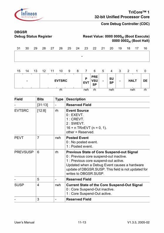
TriCore™ 132-bit Unified Processor Core
Core Debug Controller (CDC)
DBGSR Debug Status Register Reset Value: 0000 0000H (Boot Execute)
0000 0002H (Boot Halt)
31 30 29 28 27 26 25 24 23 22 21 20 19 18 17 16
-
15 14 13 12 11 10 9 8 7 6 5 4 3 2 1 0
- EVTSRC PEVT
PREVSUSP
- SUSP - HALT DE
rh rwh rh rwh rwh rh
Field Bits Type Description- [31:13] - Reserved FieldEVTSRC [12:8] rh Event Source
0 : EXEVT.1 : CREVT.2 : SWEVT.16 + n TRnEVT (n = 0, 1).other = Reserved.
PEVT 7 rwh Posted Event0 : No posted event.1 : Posted event.
PREVSUSP 6 rh Previous State of Core Suspend-out Signal0 : Previous core suspend-out inactive.1 : Previous core suspend-out active.Updated when a Debug Event causes a hardware update of DBGSR.SUSP. This field is not updated for writes to DBGSR.SUSP.
- 5 - Reserved FieldSUSP 4 rwh Current State of the Core Suspend-Out Signal
0 : Core Suspend-Out inactive.1 : Core Suspend-Out active.
- 3 - Reserved Field
User’s Manual 11-13 V1.3.5, 2005-02

TriCore™ 132-bit Unified Processor Core
Core Debug Controller (CDC)
HALT [2:1] rwh CPU Halt Request / Status FieldHALT can be set or cleared by software. HALT[0] is the actual Halt bit. HALT[1] is a mask bit to specify whether or not HALT[0] is to be updated on a software write. HALT[1] is always read as 0. HALT[1] must be set to 1 in order to update HALT[0] by software (R: read; W: write).00B R: CPU running.
W: HALT[0] unchanged.01B R: CPU halted.
W: HALT[0] unchanged.10B R: Not Applicable.
W: reset HALT[0].11B R: Not Applicable.
W: If DBGSR.DE == 1 (CDC is enabled), set HALT[0]. If DBGSR.DE == 0 (CDC is not enabled), HALT[0] is left unchanged.
DE 0 rh Debug EnableIndicates whether CDC is enabled.0 : CDC disabled.1 : CDC enabled.
Field Bits Type Description
User’s Manual 11-14 V1.3.5, 2005-02

TriCore™ 132-bit Unified Processor Core
Core Debug Controller (CDC)
EXEVT External Event Register Reset Value: 0000 0000H
31 30 29 28 27 26 25 24 23 22 21 20 19 18 17 16
-
15 14 13 12 11 10 9 8 7 6 5 4 3 2 1 0
- SUSP - BBM EVTA
rw rw rw
Field Bits Type Description- [31:6] - Reserved FieldSUSP 5 rw CDC Suspend-out Signal State
Value to be assigned to the CDC Suspend-Out signal when the Debug Event is raised.
- 4 - Reserved FieldBBM 3 rw Break Before Make (BBM) or Break After Make
(BAM) Selection0 : Break after make (BAM).1 : Break before make (BBM).
EVTA [2:0] rw Event AssociatedSpecifies the Debug Action associated with the Debug Event:000B : None; disabled.001B : Pulse BRKOUT Signal.010B : Halt and pulse BRKOUT Signal.011B : Breakpoint trap and pulse BRKOUT
Signal.100B : Software breakpoint 0 and pulse BRKOUT
Signal.101B : If implemented, software breakpoint 1 and
pulse BRKOUT Signal1).110B : If implemented, software breakpoint 2 and
pulse BRKOUT Signal1).111B : If implemented, software breakpoint 3 and
pulse BRKOUT Signal1).1) If not implemented, None.
User’s Manual 11-15 V1.3.5, 2005-02

TriCore™ 132-bit Unified Processor Core
Core Debug Controller (CDC)
CREVT Core Register Access Event Reset Value: 0000 0000H
31 30 29 28 27 26 25 24 23 22 21 20 19 18 17 16
-
15 14 13 12 11 10 9 8 7 6 5 4 3 2 1 0
- SUSP - BBM EVTA
rw rw rw
Field Bits Type Description- [31:6] - Reserved FieldSUSP 5 rw CDC Suspend-out Signal State
Value to be assigned to the CDC Suspend-out signal when the Debug Event is raised.
- 4 - Reserved FieldBBM 3 rw Break Before Make (BBM) or Break After Make
(BAM) Selection0 : Break after make (BAM).1 : Break before make (BBM).
EVTA [2:0] rw Event AssociatedSpecifies the Debug Action associated with the Debug Event:000B : None; disabled.001B : Pulse BRKOUT Signal.010B : Halt and pulse BRKOUT Signal.011B : Breakpoint trap and pulse BRKOUT
Signal.100B : Software breakpoint 0 and pulse BRKOUT
Signal.101B : If implemented, software breakpoint 1 and
pulse BRKOUT Signal1).110B : If implemented, software breakpoint 2 and
pulse BRKOUT Signal1).111B : If implemented, software breakpoint 3 and
pulse BRKOUT Signal1).1) If not implemented, None.
User’s Manual 11-16 V1.3.5, 2005-02

TriCore™ 132-bit Unified Processor Core
Core Debug Controller (CDC)
SWEVT Software Debug Event Reset Value: 0000 0000H
31 30 29 28 27 26 25 24 23 22 21 20 19 18 17 16
-
15 14 13 12 11 10 9 8 7 6 5 4 3 2 1 0
- SUSP - BBM EVTA
rw rw rw
Field Bits Type Description- [31:6] - Reserved FieldSUSP 5 rw CDC Suspend-out Signal State
Value to be assigned to the CDC Suspend-Out signal when the event is raised.
- 4 - Reserved FieldBBM 3 rw Break Before Make (BBM) or Break After Make
(BAM) Selection0 : Break after make (BAM).1 : Break before make (BBM).
EVTA [2:0] rw Event AssociatedSpecifies the Debug Action associated with the Debug Event:000B : None; disabled.001B : Pulse BRKOUT Signal.010B : Halt and pulse BRKOUT Signal.011B : Breakpoint trap and pulse BRKOUT
Signal.100B : Software breakpoint 0 and pulse BRKOUT
Signal.101B : If implemented, software breakpoint 1 and
pulse BRKOUT Signal1).110B : If implemented, software breakpoint 2 and
pulse BRKOUT Signal1).111B : If implemented, software breakpoint 3 and
pulse BRKOUT Signal1).1) If not implemented, None.
User’s Manual 11-17 V1.3.5, 2005-02

TriCore™ 132-bit Unified Processor Core
Core Debug Controller (CDC)
TR0EVT Trigger Event 0 Reset Value: 0000 0000HTR1EVT Trigger Event 1 Reset Value: 0000 0000H
31 30 29 28 27 26 25 24 23 22 21 20 19 18 17 16
- ASI
rw
15 14 13 12 11 10 9 8 7 6 5 4 3 2 1 0
ASI_EN
DU_U
DU_LR
DLR_U
DLR_LR
- SUSP - BBM EVTA
rw rw rw rw rw rw rw rw
Field Bits Type Description- [31:21] - Reserved FieldASI [20:16] Address Space Identifier
The ASI of the Debug Trigger process.ASI_EN 15 Enable ASI Compression
0 : No ASI comparison performed. Debug Trigger is valid for all processes.
1 : Enable ASI comparison. Debug Events are only be triggered when the current process ASI matches TRnEVT.ASI.
Field should be set to 0 for implementations without an MMU.
- [14:12] - Reserved FieldDU_U 11 rw Controls combinations of DU and CU
Note: Refer to Table 17, page 11-7 for clarification of trigger conditions that generate a Debug Event.0 : DU triggers event unless DU_LR == 1, where
CLR is also required.CU triggers event unless DLR_U == 1, whereDLR is also required.
1 : DU and CU only trigger an event when they are both present.
User’s Manual 11-18 V1.3.5, 2005-02
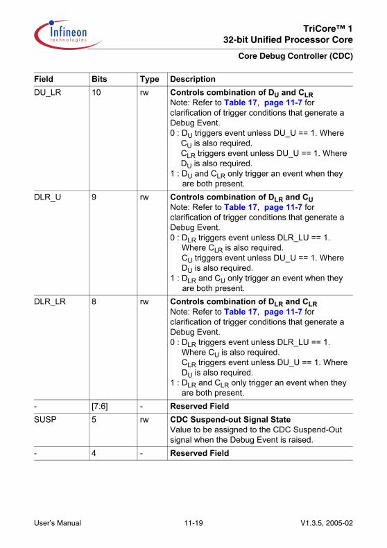
TriCore™ 132-bit Unified Processor Core
Core Debug Controller (CDC)
DU_LR 10 rw Controls combination of DU and CLRNote: Refer to Table 17, page 11-7 for clarification of trigger conditions that generate a Debug Event.0 : DU triggers event unless DU_U == 1. Where
CU is also required.CLR triggers event unless DU_U == 1. Where DU is also required.
1 : DU and CLR only trigger an event when they are both present.
DLR_U 9 rw Controls combination of DLR and CUNote: Refer to Table 17, page 11-7 for clarification of trigger conditions that generate a Debug Event.0 : DLR triggers event unless DLR_LU == 1.
Where CLR is also required.CU triggers event unless DU_U == 1. Where DU is also required.
1 : DLR and CU only trigger an event when they are both present.
DLR_LR 8 rw Controls combination of DLR and CLRNote: Refer to Table 17, page 11-7 for clarification of trigger conditions that generate a Debug Event.0 : DLR triggers event unless DLR_LU == 1.
Where CU is also required. CLR triggers event unless DU_U == 1. Where DU is also required.
1 : DLR and CLR only trigger an event when they are both present.
- [7:6] - Reserved FieldSUSP 5 rw CDC Suspend-out Signal State
Value to be assigned to the CDC Suspend-Out signal when the Debug Event is raised.
- 4 - Reserved Field
Field Bits Type Description
User’s Manual 11-19 V1.3.5, 2005-02

TriCore™ 132-bit Unified Processor Core
Core Debug Controller (CDC)
BBM 3 rw Break Before Make (BBM) or Break After Make (BAM) SelectionCode triggers BBM or BAM selection.0 : Code only triggers Break After Make (BAM).1 : Code only triggers Break Before Make (BBM).Note that data access and data/code combination access triggers can only create BAM Debug Events. When these triggers occur, TRnEVT.BBM is ignored.
EVTA [2:0] rw Event AssociatedSpecifies the Debug Action associated with the Debug Event:000B : None; disabled.001B : Pulse BRKOUT Signal.010B : Halt and pulse BRKOUT Signal.011B : Breakpoint trap and pulse BRKOUT
Signal.100B : Software breakpoint 0 and pulse BRKOUT
Signal.101B : If implemented, software breakpoint 1 and
pulse BRKOUT Signal1).110B : If implemented, software breakpoint 2 and
pulse BRKOUT Signal1).111B : If implemented, software breakpoint 3 and
pulse BRKOUT Signal1).1) If not implemented, None.
Field Bits Type Description
User’s Manual 11-20 V1.3.5, 2005-02

TriCore™ 132-bit Unified Processor Core
Core Debug Controller (CDC)
DMS Debug Monitor Start Address Reset Value: Implementation Specific
DCX Debug Context Save Area Pointer Reset Value: Implementation Specific
31 30 29 28 27 26 25 24 23 22 21 20 19 18 17 16
DMS Value
rw
15 14 13 12 11 10 9 8 7 6 5 4 3 2 1 0
DMS Value -
rw
Field Bits Type DescriptionDMS Value [31:1] rw Debug Monitor Start Address
DMS Value = DE00 00n0H, where ‘n’ is Core ID.- 0 - Reserved
31 30 29 28 27 26 25 24 23 22 21 20 19 18 17 16
DCX Value
rw
15 14 13 12 11 10 9 8 7 6 5 4 3 2 1 0
DCX Value -
rw
Field Bits Type DescriptionDCX Value [31:4] rw Debug Context Save Area Pointer
DCX Value = DE80 0000H.- [3:0] - Reserved
User’s Manual 11-21 V1.3.5, 2005-02

TriCore™ 132-bit Unified Processor Core
Core Debug Controller (CDC)
11.5.1 Software Breakpoint Service Request Control RegisterThe Software Breakpoint Service Request Control Register (SBSRCn) defines theinterrupt request parameters for a software breakpoint interrupt, where n = 0, 1, 2 or 3.
31 30 29 28 27 26 25 24 23 22 21 20 19 18 17 16
-
15 14 13 12 11 10 9 8 7 6 5 4 3 2 1 0
SETR
CLRR SRR SRE TOS - SRPN
w w rh rw rw rw
Field Bits Type Description- [31:16] - Reserved FieldSETR 15 w Service Request Set
SETR is required to set SRR.0 : No action.1 : Set SRR. Written value is not stored. Read always
returns 0. No action if CLRR is also set.CLRR 14 w Service Request Clear
CLRR is required to set SRR.0 : No action.1 : Clear SRR. Written value is not stored. Read always
returns 0. No action if SETR is also set.SRR 13 rh Service Request Flag
0 : No Software Breakpoint Service Request is pending.1 : A Software Breakpoint Service Request is pending.
SRE 12 rw Service Request Enable0 : Software Breakpoint Service Request is disabled.1 : Software Breakpoint Service Request is enabled.
TOS [11:10] rw Type Of Service Control00B : Service Provider 0 - Typically CPU service is
initiated.01B : Service Provider 1 - Implementation Specific.10B : Service Provider 2 - Implementation Specific.11B : Service Provider 3 - Implementation Specific.
- [9:8] - Reserved Field
User’s Manual 11-22 V1.3.5, 2005-02

TriCore™ 132-bit Unified Processor Core
Core Debug Controller (CDC)
SRPN [7:0] rw Service Request Priority Number00H : Software Breakpoint Service Request is never
serviced.01H : Software Breakpoint Service Request,
lowest priority.…FFH : Software Breakpoint Service Request,
highest priority.
Field Bits Type Description
User’s Manual 11-23 V1.3.5, 2005-02

TriCore™ 132-bit Unified Processor Core
Core Debug Controller (CDC)
User’s Manual 11-24 V1.3.5, 2005-02

TriCore™ 132-bit Unified Processor Core
Floating Point Unit (FPU)
12 Floating Point Unit (FPU)This chapter describes the TriCore™ Floating Point Unit (FPU) architecture. The FPU isan optional component in TriCore configurations. It need not be present in every systemthat uses the core, and even when present it can be disabled.The optional FPU is an IEEE-754 compatible floating-point unit to accompany theTriCore™ instruction set.
12.1 Functional OverviewThe FPU executes single precision IEEE-754 compatible floating-point arithmeticinstructions and supports the following feature set:• Floating-point add, subtract, multiply, MAC, and divide instructions.• Conversion to or from IEEE-754 single precision format from or to TriCore signed and
unsigned integers and 32-bit signed fractions (Q31 format).• QSEED.F instruction used to obtain an approximate value intended for use in
Newton-Raphson iterations to perform a square-root operation.• Comparison of two floating-point numbers.• All four IEEE-754 rounding modes are implemented.
RestrictionsThe FPU has the following restrictions and usage limitations:• Only IEEE-754 single precision format is supported.• IEEE-754 denormalized numbers are not supported for arithmetic operations.• IEEE-754 compliant remainder function cannot be implemented using FPU
instructions because of the effects of multiple rounding when using a sequence ofindividually rounded instructions.
• Fused multiply-and-accumulate operations (MACs) are not part of the IEEE-754standard. Using FPU MAC operations can give different results from using separatemultiply and accumulate operations because the result is only rounded once at theend of a MAC.
• Full compliance with the IEEE-754 standard is not achieved because denormalnumbers are not supported.
User’s Manual 12-1 V1.3.5, 2005-02

TriCore™ 132-bit Unified Processor Core
Floating Point Unit (FPU)
12.2 IEEE-754 Compliance
12.2.1 IEEE-754 Single Precision Data Format
Figure 45 Single Precision IEEE-754 Floating-Point Format
The single precision IEEE-754 floating-point format has three sections: a sign bit, an8-bit biased exponent, and a 23-bit fractional mantissa with an implied binary pointbefore bit 22. For normal numbers the mantissa has an implied 1 immediately to the leftof the binary point. Table 20 shows the different types of number representation inIEEE-754 single precision format. In this table:s = bit [31]: sign bit.e = bits [30:23]: biased exponent.f = bits [22:0]: fractional part of mantissa.
Note: Both signed values of zero are always treated identically and never producedifferent results except different signed zeros.
Table 20 IEEE-754 Single Precision Representation TypesCondition Represented Value Description0 < e < 255 (-1)s*2(e-127)*1.f Normal number.e == 0 AND f != 0 (-1)s*2(-126)*0.f Denormal number.e == 0 AND f == 0 (-1)s*0 Signed zero.s == 0 AND e == 255 AND f == 0 + ∞ + infinity.s == 1 AND e == 255 AND f == 0 - ∞ – infinity.e == 255 AND f != 0 AND f[22] == 0 Signalling NaN1).
1) IEEE-754 does not define how to distinguish between signalling NaNs and quiet NaNs, but bit[22] has becomethe standard way of doing this.
e == 255 AND f != 0 AND f[22] == 1 Quiet NaN1).
User’s Manual 12-2 V1.3.5, 2005-02

TriCore™ 132-bit Unified Processor Core
Floating Point Unit (FPU)
12.2.2 Denormal NumbersDenormal numbers are not supported for arithmetic operations. With the exception of theCMP.F instruction, all instructions replace denormal operands with the appropriatelysigned zero before computation. Following computation, if a denormal number wouldotherwise be the result, it is replaced with the appropriately signed zero.Conceptually, the conventional order for making IEEE-754 computations is:1. Compute result to infinite precision.2. Round to IEEE-754 format.This is replaced with:1. Substitute signed zero for all denormal operands.2. Compute result to infinite precision.3. Round to IEEE-754 format.4. Substitute signed zero for all denormal results.This procedure has a subtle effect on underflow; see Round to Nearest: Denormalsand Zero Substitution, page 12-7.Denormal numbers are supported only by the CMP.F instruction which makescomparisons of denormal numbers in addition to identifying denormal operands.
12.2.3 NaNs (Not a Number)NaNs (Not a Number) are bit combinations within the IEEE-754 standard that do notcorrespond to numbers. There are two types of NaNs: signalling and quiet. The FPUdefines signalling NaNs to have bit 22 = ‘0’, and quiet NaNs to have bit 22 = ‘1’.When invalid operations are performed (including operations with a signalling NaNoperand), FI is asserted and a quiet NaN is produced as the floating-point result. Thequiet NaN contains information about the origin of the invalid operation; see InvalidOperations and their Quiet NaN Results, page 12-10.IEEE-754 suggests that quiet NaNs should be propagated so that the result of aninstruction receiving a quiet NaN as an operand (with no signalling NaN operands)should be that quiet NaN. The FPU does not propagate quiet NaNs in this way. Theresult of an operation that has one (or more) quiet NaN operands and no signalling NaNoperands is always the quiet NaN 7FC00000H.
User’s Manual 12-3 V1.3.5, 2005-02

TriCore™ 132-bit Unified Processor Core
Floating Point Unit (FPU)
12.2.4 UnderflowUnderflow occurs when the result of a floating-point operation is too small to store infloating-point representation.IEEE-754 requires two conditions to occur before flagging underflow:• The result must be ‘tiny’.
– A result is ‘tiny’ if it is non-zero and its magnitude is < 2-126 (for single precision).IEEE-754 allows this to be detected either before or after rounding.
• There must be a loss of accuracy in the stored result.Loss of accuracy can be detected in two ways: either as a denormalization loss, or aninexact result.Denormalization loss occurs when the result is calculated assuming an unboundedexponent, but is rounded to a normalized number using 23 fractional bits. If this roundedresult must be denormalized to fit into IEEE-754 format and the resultant denormalizednumber differs from the normalized result with unbounded exponent range, then adenormalization loss occurs.An inexact result is one where the infinitely precise result differs from the value stored.The FPU determines tininess before rounding and inexact results to determine loss ofaccuracy.In the case of the FPU, even if a denormal result would produce no loss of accuracy,because it is replaced with a zero, accuracy is lost and underflow must be flagged.Any tiny number that is detected must therefore result in a loss of accuracy since it willeither be a denormal that is replaced with zero or rounded up. Therefore underflowdetection can be simplified to tiny number detection alone; i.e. any non-zero unroundednumber whose magnitude is < 2-126.
12.2.5 Fused MACsFused multiply-and-accumulate operations (MACs) are not supported by the IEEE-754standard. Using FPU MAC operations (MADD.F and MSUB.F) can give different resultsfrom using separate multiply (MUL.F) and accumulate (ADD.F or SUB.F) operationsbecause the result is only rounded once at the end of a MAC.
User’s Manual 12-4 V1.3.5, 2005-02
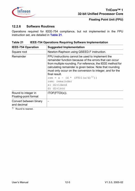
TriCore™ 132-bit Unified Processor Core
Floating Point Unit (FPU)
12.2.6 Software RoutinesOperations required for IEEE-754 compliance, but not implemented in the FPUinstruction set, are detailed in Table 21.
Table 21 IEEE-754 Operations Requiring Software ImplementationIEEE-754 Operation Suggested ImplementationSquare root Newton-Raphson using QSEED.F instruction.Remainder FPU instructions cannot be used to implement the
remainder function because of the errors that can occur from multiple rounding. For reference, the IEEE method for calculating remainder is given below. Note that rounding must only occur on the conversion to integer, and for the final result.rem = x - (d * (FTOI(x/d)1)))rem: remainderx: dividendd: divisor
1) Round to nearest.
Round to integer in Floating-point format
ITOF(FTOI(x)).
Convert between binary and decimal
-
User’s Manual 12-5 V1.3.5, 2005-02

TriCore™ 132-bit Unified Processor Core
Floating Point Unit (FPU)
12.3 RoundingAll four rounding modes specified in IEEE-754 are supported. The rounding mode isselected using the RM field of the PSW (PSW[25:24]).
IEEE-754 defines the rounding modes in terms of representable results, in relation to the‘infinitely precise’ result. The infinitely precise result is the mathematically exact resultthat would be computed by the operation, if the number of mantissa and exponent bitswere unlimited.• Round to nearest is defined as returning the representable value that is nearest to
the infinitely precise result. This is the default rounding mode that should be selectedwhen RTOS software initializes a task. See Round to Nearest: Even, page 12-7, forfurther information.
• Round toward + ∞ is defined as returning the representable value that is closest toand no less than the infinitely precise result.
• Round toward – ∞ is defined as returning the representable value that is closest toand no greater than the infinitely precise result.
• Round toward zero is defined as returning the representable value that is closest toand no greater in magnitude than the infinitely precise result. It is equivalent totruncation.
The rounding mode can be changed by the UPDFL (Update Flags) instruction.Rounding is performed at the end of each relevant FPU instruction, followed by thereplacement of all denormal numbers with the appropriately signed 0.IEEE-754 does not specify the MAC instructions (MADD.F and MSUB.F) that combinemultiplication and addition in a single operation. The result from the multiply part of aMAC instruction is not rounded before it is used in the addition in the FPU. Instead thewhole MAC is calculated with infinite precision and rounded at the end of the add. It istherefore possible that the result from a MADD.F instruction will differ from the result thatwould be obtained using the same operands in a MUL.F followed by an ADD.F.
Table 22 Rounding Mode DefinitionRounding Mode Value Mode001)
1) Round to nearest is the default rounding mode.
Round to nearest.01 Round toward + ∞.
01 Round toward - ∞.11 Round toward zero.
User’s Manual 12-6 V1.3.5, 2005-02

TriCore™ 132-bit Unified Processor Core
Floating Point Unit (FPU)
12.3.1 Round to Nearest: Even‘Round to nearest’ is defined as returning the representable value that is nearest to theinfinitely precise result. If two representable values are equally close (i.e. the infinitelyprecise result is exactly half way between two representable values), then the one whoseLSB (Least Significant Bit) is zero is returned. This is sometimes known as rounding tonearest even.This is usually straight forward, but if the infinitely precise result is half way between tworepresentable numbers with different exponents, the result with the larger exponent isalways selected (the LSB of its mantissa is zero).For example, if the infinitely precise result is:1.111 1111 1111 1111 1111 1111 1000 0000 0000B * 20
This is half way between:1.0000 0000 0000 0000 0000 000B * 21
and:1.111 1111 1111 1111 1111 1111B * 20
The result with the larger exponent is returned.
12.3.2 Round to Nearest: Denormals and Zero SubstitutionFollowing computation, results are first rounded to IEEE-754 representable numbersand then the appropriately signed zero is substituted for any denormal results that mayhave occurred. This produces some results that can seem counter intuitive.Consider an infinitely precise result that has been computed and falls between thesmallest representable positive IEEE-754 normal number (1.000 … 000 * 2-126) and thelargest representable positive IEEE-754 denormal number (0.111 … 111 * 2-126).• If the infinitely precise result is nearer to the normal number, or halfway between the
two, then the result must be rounded to the normal number.• If the infinitely precise result is nearer to the denormal number, then the result is
rounded to the denormal value. Zero is then substituted for the denormal result.The FPU implementation cannot produce denormal results, however the concept ofdenormal numbers is important to the FPU implementation in this instance. It would bewrong to assume that the infinitely precise result should be rounded to the nearest FPUrepresentable number, in this case (+1.000 … 000 * 2-126) or (0). Such animplementation would mean that all unrounded results between (+1.000 … 000 * 2-126)and (+0.100 … 000 * 2-126) would be rounded to the smallest representable positiveIEEE-754 normal number.
User’s Manual 12-7 V1.3.5, 2005-02

TriCore™ 132-bit Unified Processor Core
Floating Point Unit (FPU)
12.3.3 Round Towards ± ∞: Denormals and Zero SubstitutionFollowing computation results are first rounded to IEEE-754 representable numbers,then the appropriately signed zero is substituted for any denormal results that may haveoccurred. See Denormal Numbers, page 12-3.According to the IEEE-754 definition of the rounding modes, when rounding towards + ∞(- ∞ ) the rounded result should not be less than (greater than) the infinitely precise result.However if a positive (negative) result would otherwise be rounded to a denormalnumber, it is then substituted for a zero. Therefore the returned result of zero is less than(greater than) the infinitely precise result. The returned result appears to contradict thedefinition of these rounding modes in this case.
User’s Manual 12-8 V1.3.5, 2005-02

TriCore™ 132-bit Unified Processor Core
Floating Point Unit (FPU)
12.4 ExceptionsThe FPU implements all five IEEE-754 exceptions (invalid operation, overflow, divide byzero, underflow, and inexact). When one of these exceptions occur the correspondingexception flag in the PSW is asserted.The IEEE-754 exception flags are stored as part of the PSW register as shown in thefollowing table. In accordance with IEEE-754, each bit is sticky so that the FPUinstructions in general assert these flags when an exception occurs and do not negatethem when the exception does not occur. The UPDFL instruction can be used to clearthe exception flags.
Since the IEEE-754 exception flags are sticky, it can be impossible to tell if an exceptionoccurred on the last instruction if it was asserted before the last instruction executed. Anadditional, non sticky, exception flag (FS) is therefore implemented to identify if the lastFPU instruction caused an IEEE-754 exception or not.Note that the PSW bits used to store the exception flags are also used to store ALU flagsas shown in the table above. When an ALU instruction updates these flags, thecorresponding FPU exception flag is overwritten and lost.The following conditions are true for all FPU operations asserting exception flags, withthe exception of UPDFL.• Any FPU operation can assert only one of the FI, FV, FZ or FU exception flags.• FX can be asserted by any operation so long as FI and FZ are negated.• When either FV or FU are asserted, FX is also asserted.
FS - Some ExceptionThis bit is not sticky and is asserted or negated for all instructions that can causeIEEE-754 exceptions to occur. If any of the IEEE-754 exceptions (FI, FV, FZ, FU, FX)have occurred during that instruction, FS is also asserted.Note: UPDFL can assert IEEE-754 exceptions without asserting FS.
Table 23 FPU Exception FlagsALU Flag FPU Flag FPU Exception PSW Bit PositionC FS Some Exception. 31V FI Invalid Operation. 30SV FV Overflow. 29AV FZ Divide by Zero. 28SAV FU Underflow. 27- FX Inexact. 26
User’s Manual 12-9 V1.3.5, 2005-02

TriCore™ 132-bit Unified Processor Core
Floating Point Unit (FPU)
FI - Invalid OperationFI is asserted in three circumstances:• When a signalling NaN (see NaNs (Not a Number), page 12-3) is an operand for a
FPU instruction.• For invalid operations such as QSEED.F (≈1/√ x) of a negative number.• Conversions from floating-point to other formats where the rounded result is outside
the range of the target.When an instruction that produces a floating-point result asserts FI as a result of asignalling NaN or invalid operation, the result is a quiet NaN.
Table 24 Invalid Operations and their Quiet NaN ResultsInvalid Operation Quiet NaNSignalling NaN operand for arithmetic instructions.1)
1) Also see the FPU operation syntax description in the Instruction Set.
7FC00000H2)
2) The quiet NaN (7FC00000H) is produced as the result of arithmetic operations that have any NaN as anoperand. FI is only asserted when one of these NaNs is signalling. See NaNs (Not a Number), page 12-3.
Signalling NaN operand for CMP.F instruction. n.a.5)
ADD.F with + ∞ and - ∞ as operands. 7FC00001H
SUB.F with (+ ∞ and + ∞ ) or (- ∞ and - ∞ ) as operands. 7FC00001H
MADD.F if the result of the multiplication is ± ∞ and the addend is the oppositely signed ∞.
7FC00001H
MSUB.F if the result of the multiplication is ± ∞ and the minuend is the same signed ∞.
7FC00001H
MUL.F with 0 and ± ∞ as multiplicands. 7FC00002H
MADD.F with 0 and ± ∞ as multiplicands. 7FC00002H
MSUB.F with 0 and ± ∞ as multiplicands. 7FC00002H
QSEED.F with a negative operand3).
3) -0 is not negative, therefore QSEED.F of -0 is -∞.
7FC00004H
DIV.F with 0 as both operands4).
4) 0/0 is defined as being an invalid operation (FI) rather than a divide by zero (FZ).
7FC00008H
DIV.F with both operands being an ∞ of either sign. 7FC00008H
FTOI, FTOU or FTOQ31 with rounded result outside the range of the target format.
n.a.5)
5) The result is not in floating-point format and therefore cannot be a quiet NaN. Refer to the instructiondescription for what the result should be.
FTOI, FTOU or FTOQ31 with the input operand a quiet NaN, a signalling NaN or ± ∞.
n.a.5)
User’s Manual 12-10 V1.3.5, 2005-02

TriCore™ 132-bit Unified Processor Core
Floating Point Unit (FPU)
FV - OverflowFor operations that return a floating-point result, the FV flag is set as stated in IEEE-754;‘whenever the destination format’s largest finite number is exceeded in magnitude bywhat would have been the rounded floating-point result, were the exponent rangeunbounded’.The result returned is determined by the rounding mode and the sign of the unroundedresult:• Round to nearest carries all overflows to infinity, with the sign of the unrounded result.• Round toward zero carries all overflows to the format’s largest finite number with the
sign of the unrounded result.• Round toward minus infinity carries positive overflows to the format’s largest finite
number, and carries negative overflows to minus infinity.• Round toward plus infinity carries negative overflows to the format’s most negative
finite number, and carries positive overflows to plus infinity.When overflow is flagged (FV asserted), the returned result can not be exactly equal tothe unrounded result. Therefore whenever FV is asserted FX is also asserted.
FZ - Divide by ZeroThe FZ flag is set by DIV.F if the divisor operand is zero and the dividend operand is afinite non zero number. The result is an infinity with sign determined by the usual rules.Note that:• 0/0 is defined as an invalid operation, so FI is asserted rather than FZ.• All arithmetic with ± ∞ as an operand is defined as being exact, except for invalid
operations where FI is asserted. Therefore for ± ∞ / ± 0 FZ is not asserted, theappropriately signed ∞ is returned as the result with no other exceptions occurring.
FU - UnderflowAs discussed in Underflow, page 12-4, underflow is detected and so FU is asserted,when the unrounded result is smaller in magnitude than the smallest representablenormal number (2-126).The Q31TOF instruction can cause an underflow as well as the arithmetic instructionsADD.F, SUB.F, MUL.F, MADD.F, MSUB.F, and DIV.F.The return result for instructions flagging an underflow are complicated by the way thatFPU treats denormal numbers. This is described in detail in Round to Nearest:Denormals and Zero Substitution, page 12-7.
FX - InexactIf the rounded result of an operation is not exactly equal to the unrounded result, thenthe FX flag is set.
User’s Manual 12-11 V1.3.5, 2005-02

TriCore™ 132-bit Unified Processor Core
Floating Point Unit (FPU)
The result delivered is the rounded result, unless either overflow (FV) or underflow (FU)has also occurred during this instruction, when the overflow or denormalization returnresult rules are followed.
User’s Manual 12-12 V1.3.5, 2005-02

TriCore™ 132-bit Unified Processor Core
Glossary
13 Glossary
Reference DefinitionAddend A number to be added to another number.API Application Program Interface - A set of routines, protocols
and tools for building software applications.ASI Address Space Identifier - A TTE field. ASIC Application Specific Integrated Circuit.ATPG Automatic Test Pattern GenerationAV Advance Overflow - PSW status flag.Ax Address Registers.BCU Bus Control Unit.Biased exponent The sum of the exponent and a constant (bias) chosen to
make the biased exponent’s range non-negative.BISR Begin Interrupt Service Routine.BIST Built-In Self Test.BIV Base Address of Interrupt Vector Table.BPI Bus Peripheral InterfaceBTV Base Address of Trap Vector Table.CALL Function call instruction.CCPN Current CPU Priority Number.CDC Call Depth Control field.CLO Count Leading Ones.CLS Count Leading Signs.CLZ Count Leading Zeros.CMOV Conditional Move instruction.Context Every Task has a Context. The Context is everything the
processor needs in order to define the state of the associated task and enable its continued execution. Context’s are subdivided into Upper & Lower Contexts.
CPM Code Protection Mode.CPR Code Segment Protection Register.CPS CPU Slave.
User’s Manual 13-1 V1.3.5, 2005-02

TriCore™ 132-bit Unified Processor Core
Glossary
CPU Central Processing Unit.CREVT Core Register Access Event Register.
Emulator Resource Protection Event register.CSA Context Save Area.
Each CSA can hold 1 upper or 1 lower Context. CSAs are linked together through a Link Word.
CSFR Core Special Function Register (SFR).CVE Core Verification Environment.CVE Co-Verification Environment.DBGSR Debug Status Register.DC Direct Current.DCU Data Control Unit.DCX Debug Context Save Area Pointer Register.DEC Decode Pipeline stage.Denormalized number A non-zero floating-point number whose exponent has the
format’s minimum, and whose implicit leading mantissa bit is zero.
DFF D-type Flip Flop.Dividend A number to be divided by the divisor.Divisor A number by which a dividend is divided.DMA Direct Memory Access.DMS Debug Monitor Start Address Register.DMU Data Memory Unit.DPM Data Protection Mode.DPR Data Segment Protection Register.DRAM Direct Random Access Memory.DSP Digital Signal Processing.Dx Data Registers.EBU External Bus Unit.EDA Electronic Design Automation.EMU Emulation Monitoring Unit.EQ Equal - compare instruction.
Reference Definition
User’s Manual 13-2 V1.3.5, 2005-02

TriCore™ 132-bit Unified Processor Core
Glossary
EX1 Execute 1 pipeline stage.EX2 Execute 2 pipeline stage.EXEVT External Event Register.Exponent The component of a binary floating-point number that normally
signifies the integer power to which 2 is raised in determining the value of the represented number.
FCD Free Context list Depletion trap.FFT Fast Fourier Transformations.FI Flag Invalid exception.FPD Fetch and Pre-decode.FPI Flexible Peripheral Interface - Used for on-chip
interconnections, connecting the core with peripherals including ports and the External Bus Controller.
FPU Floating Point Unit.FPU Floating-Point Unit.FS Flag some exception.FU Flag underflow exception.FV Flag overflow exception.FX Flag inexact exception.FZ Flag divide by zero exception.GDI Graphical Device Interface.GE Greater Than or Equal to - compare instruction.GPR General Purpose Register.GPTU General Purpose Timer Unit.GRWP Global Register Write Protection.HLL High Level Language.I/F Interface.IC Integrated Circuit.ICR Interrupt Unit Control Register.ICU Interrupt Control Unit.ID Identity / Identification.IE Interrupt Enable.
Reference Definition
User’s Manual 13-3 V1.3.5, 2005-02

TriCore™ 132-bit Unified Processor Core
Glossary
IEEE Institute of Electrical & Electronics Engineers.IIR Infinite Impulse Response
A digital filter with internal registers that hold past output of the filter.
Infinite precision The result of a floating-point operation assuming unbounded exponent and mantissa bits.
IOPC Illegal Opcode.IS Interrupt Stack.ISA Instruction Set Architecture.ISP Interrupt Stack Pointer.ISR Interrupt Service Routine.JTAG Joint Test Action Group.LDCUX Instruction to Load Upper Context from memory.LDLCX Instruction to Load Lower Context from memory.LDMST Load Modify Store instruction.LEA Load Effective Address.LEADDR LMB Error Address.LEATT LMB Error Attributes.LEDAT LMB Error Data.LFI LMB to FPI Interface: A bridge between the two main buses,
LMB and FPI.LMU Local Memory Unit.LT Less Than - compare instruction.MAC Multiply and Accumulate.MAC Multiply and Accumulate.Mantissa Tthe component of a binary floating-point number that consists
of the implicit leading bit to the left of the implied binary point, and the fractional field.
MCU MicroController Unit.Minuend A number from which a subtrahend is to be subtracted.MIPS Million Instructions Per Second.
Reference Definition
User’s Manual 13-4 V1.3.5, 2005-02

TriCore™ 132-bit Unified Processor Core
Glossary
MMU Memory Management Unit - translates virtual addresses issued by the load / store, instruction fetch unit into physical addresses to feed into the PMU and DMU respectively.
MTCR Move To Control Register.Multiplicand A number to be multiplied by another number.NaN Not a Number.NE Not Equal compare instruction.NMI Non-Maskable Interrupt.Normalized number A floating-point number whose implicit leading mantissa bit is
one.OCDS On-Chip Debug Support.Operand Data that is to be operated on.OTP One-Time Programmable.PC Program Counter.PCP Peripheral Control Processor - an I/O control processor that
performs tasks typically handled by a dedicated DMA controller and CPU interrupt service routines.
PCPN Previous CPU Priority Number.PCXI Previous Context Information Register.PIPN Pending Interrupt Priority Number.PMU Program Memory Unit.PPN Physical Page Number (see Address Spaces).PRS Protection Register Set (see Memory Protection System).PSW Processor Status Word.PTE Page Table Entry (see Address Translation).Quotient The number resulting from the division of one number by
another.RA Return Address register.RAM Random Access Memory.Remainder The final undivided part after division that is less or of lower
degree than the divisor.RET Return from CALL instruction.
Reference Definition
User’s Manual 13-5 V1.3.5, 2005-02

TriCore™ 132-bit Unified Processor Core
Glossary
RFE Return From Exception - return from an interrupt or trap handler.
RISC Reduced Instruction Set Computer.RM Rounding Mode.ROM Read Only Memory.Rounded result The infinitely precise result rounded to fit into IEEE-754 format.RSLCX Restore Lower Context instruction.RSTV Reset Overflow Bits.RTL Register Transfer Level.RTOS Real-Time Operating System.SAV Sticky Advance Overflow - PSW status flag.SDF Standard Delay Format.SFR Special Function Register.SFR Special Function Register.Significand See mantissa.SIMD Single Instruction Multiple Data.SMT Software Managed Tasks.SOC System-On-a-Chip.SP Stack Pointer.SPR Scratch Pad RAM.SRAM Static Random Access Memory.SRE Software Request Enable field in the SRC register.SRN Service Request Node.SRPN Service Request Priority Number.STA Static Timing Analysis.STLCX Store Lower Context instruction.STPG Static Test Pattern Generation.STUCX Store Upper Context.Subtrahend A number that is to be subtracted from a minuend.SV Sticky Overflow - PSW status flag.SVLCX Save Lower Context instruction.
Reference Definition
User’s Manual 13-6 V1.3.5, 2005-02

TriCore™ 132-bit Unified Processor Core
Glossary
SWEVT Software Debug Event Register.SYSCON System Control Register.Task Refers to an independent thread of control. There are two
types of tasks: Software Managed Tasks (SMTs) and Interrupt Service Routines (ISRs).
TC Abbreviation for TriCore (TriCore 1 or TriCore 2, for example).TFA Translation Fault Address.TIN Trap Identification Number - Identifies the cause of a trap
within its class (TriCore has 8 Trap classes).TLB Translation Lookaside Buffer.TOS Type Of Service field.TPA Translation Physical Address.TPX Translation Page Index.TRAPSV Trap on Sticky Overflow instruction.TRAPV Trap on Overflow instruction.TRnEVT Trigger Event n Specifier register.TSIM TriCore Instruction Set Simulator (Tricore SIMulator) - A
configurable, instruction-accurate model of the TriCore core architecture, providing a simulation environment that models the core, memory configuration and interrupt mechanism. Used for debugging and developing customized designs.
TTE TLB Table Entries (see Memory Management).UL Upper Lower context.Unrounded result The infinitely precise result.UOPC Unimplemented Opcode.V Overflow - PSW status flag.VAP Virtual Address Protection trap.VPN Virtual Page Number.WB Write Back pipeline stage.
Reference Definition
User’s Manual 13-7 V1.3.5, 2005-02

TriCore™ 132-bit Unified Processor Core
Glossary
User’s Manual 13-8 V1.3.5, 2005-02

TriCore™ 132-bit Unified Processor Core
List of Registers
14 List of RegistersA[10](SP) . . . . . . . . . . . . . . . . . . 4-22BIV . . . . . . . . . . . . . . . . . . . . . . . . 4-25BTV . . . . . . . . . . . . . . . . . . . . . . . 4-26CPMx . . . . . . . . . . . . . . . . . . . . . . 9-8CPRx_nL . . . . . . . . . . . . . . . . . . . 9-5CPRx_nU . . . . . . . . . . . . . . . . . . . 9-5CPU_ID . . . . . . . . . . . . . . . . . . . . 4-28CREVT . . . . . . . . . . . . . . . . . . . . 11-16DBGSR . . . . . . . . . . . . . . . . . . . . 11-13DCX . . . . . . . . . . . . . . . . . . . . . . 11-21DMS . . . . . . . . . . . . . . . . . . . . . . 11-21DPMx . . . . . . . . . . . . . . . . . . . . . . 9-6DPRx_nL . . . . . . . . . . . . . . . . . . . 9-4DPRx_nU . . . . . . . . . . . . . . . . . . . 9-4EXEVT . . . . . . . . . . . . . . . . . . . . 11-15FCX . . . . . . . . . . . . . . . . . . . . . . . 4-18ICR . . . . . . . . . . . . . . . . . . . . . . . . 4-23ISP . . . . . . . . . . . . . . . . . . . . . . . 4-22LCX . . . . . . . . . . . . . . . . . . . . . . . 4-20MMU_ASI . . . . . . . . . . . . . . . . . . 10-15MMU_CON . . . . . . . . . . . . . . . . . 10-13MMU_TFA . . . . . . . . . . . . . . . . . . 10-20MMU_TPA . . . . . . . . . . . . . . . . . . 10-17MMU_TPX . . . . . . . . . . . . . . . . . . 10-19MMU_TVA . . . . . . . . . . . . . . . . . . 10-16mod_SRCn . . . . . . . . . . . . . . . . . 6-3PC . . . . . . . . . . . . . . . . . . . . . . . . 4-10PCX . . . . . . . . . . . . . . . . . . . . . . . 4-19PCXI . . . . . . . . . . . . . . . . . . . . . . 4-16PSW . . . . . . . . . . . . . . . . . . . . . . . 4-11SWEVT . . . . . . . . . . . . . . . . . . . . 11-17SYSCON . . . . . . . . . . . . . . . . . . . 4-27TR0EVT . . . . . . . . . . . . . . . . . . . 11-18TR1EVT . . . . . . . . . . . . . . . . . . . 11-18
User’s Manual 14-1 V1.3.5, 2005-02

TriCore™ 132-bit Unified Processor Core
List of Registers
User’s Manual 14-2 V1.3.5, 2005-02

TriCore™ 132-bit Unified Processor Core
Index
15 Index
AA0, A1, A8, A9
System Global RegistersGPRs 4-7Overview 2-4
A0-A15Address Registers 4-2
A10Stack Pointer 4-21
AbsoluteAddressing 3-8
AddressAbsolute 3-13Array 3-11Base Address of Vector Table 4-25Code 3-13Definition 3-2Displacement 3-6Effective 3-11, 4-17General Purpose Registers 4-7Half-word 4-26Map 2-5
Physical Memory Attributes 8-3Mapping 2-5Multiple Address Spaces 10-5Physical Memory 5-5Range 9-12Ranges 5-5Register 3-13
Use with GPRs 4-7Register A10 4-21Return Address A11 4-7Space 2-1, 2-5Space Identifier (ASI) 10-1, 10-5Spaces 10-2Width 3-6
Address RegisterDefinition 4-22
Address Translation 10-3Context Pointers 10-3
MMU_CON 10-3PPN 10-3PTE 10-3VPN 10-3
AddressingAbsolute 3-8Address Register 3-9Base + Offset 3-8Bit Indexed 3-12Bit Reverse 3-11Circular 3-9Indexed 3-12Modes 2-5, 3-7
Programming Model 3-1, 3-7Synthesized 3-12
PC-relative 3-13Post-decrement 3-9Post-increment 3-9Pre-decrement 3-8Pre-Increment 3-8Synthesized 3-12
ADDSC.A InstructionIndexed Addressing 3-12
ADDSC.AT 3-12Alignment
Requirements 3-4Rules 3-4Trap 3-10
ALN TrapData Address Alignment 7-9
ArbitrationScheme 6-8
Architectural Registers 2-3Architecture
Addressing Data 3-13Overview 2-1Traps 7-1
ArrayIndex 3-11
ASIAddress Space Identifier 10-1, 10-5Field in MMU_ASI Register 10-15Field in MMU_TVA Register 10-16
User’s Manual 15-1 V1.3.5, 2005-02

TriCore™ 132-bit Unified Processor Core
Index
Field in TRnEVT Register 11-18ASI_EN
Field in TRnEVT Register 11-18Assertion Traps 7-13Associativity (of TLB) 10-4Asynchronous Traps 7-3Automatic Switch
Stack Management 4-21
BBAM Trap
Break After Make 7-13Priority of Debug Events 11-4
Base+ Offset Addressing 3-8Address 3-11Register 3-13
Base + Offset Addressing 3-8BBM
Debug Halt Action 11-9Field in CREVT Register 11-16Field in EXEVT Register 11-15Field in SWEVT Register 11-17Field in TRnEVT Register 11-20Priority of Debug Events 11-4Trap
Break Before Make 7-13BISR Instruction
Context Switching with Interrupts 5-7Bit
Bit-Reverse Addressing 3-11Enable and Disable 4-23String 3-1Type Abbreviations 1-2
Bit TypeAbbreviations in Tables
Definitions 1-2Bit-Reverse Addressing 3-11Bit-Reversed Order 3-11BIV
RegisterAddress Offset 4-3Definition 4-25
Interrupt and Trap Handling 4-23BL
Field in CPMx Register 9-8Boolean
Programming Model 3-1Breakpoint
CDC Features 11-1Interrupt Debug Action 11-10Trap 11-9
BTVBase Trap Vector Table Pointer 4-26Register
Address Offset 4-3Definition 4-26Interrupt and Trap Handling 4-23
BUField in CPMx Register 9-9
BufferAligned to a 64-bit Boundary 3-10Size 3-12Start 3-10
ByteDefinition 1-2Indices 3-12Offset 3-10Ordering 3-5
CC
Field in MMU_TPA Register 10-18Cacheability Bit (C)
TLB Table Entry Contents 10-5Cacheable (C)
Physical Memory Address Properties 8-1
Cacheable MemoryPhysical Memory Attribute 8-3
Call Depth CounterCSAs and Context Lists 5-6Field in PSW Register 4-14NEST Trap 7-12
CALL InstructionContext Switching & Calls 5-8
User’s Manual 15-2 V1.3.5, 2005-02

TriCore™ 132-bit Unified Processor Core
Index
Calling and Called Functions 5-8CCPN
CPU PriorityInterrupt Priority Groups 6-12
Current CPU Priority Number 4-23Field in ICR Register 4-24
CDCCombining Debug Triggers 11-7Control Registers 11-12Core Debug Controller 11-1Debug Triggers 11-6Enabling 11-1Features 11-1Memory Protection System 9-1Priority of Debug Events 11-4
CDEField in PSW Register 4-13
CDO TrapCall Depth Overflow 7-11
CDU TrapCall Depth Underflow 7-11
CircularAddressing 3-9, 3-10Buffer
Circular Addressing 3-9, 3-10End Case 3-10Restrictions 3-10
CLRRDescription 6-4Field in SRC Register 6-3
CodeAddress 3-13Fetch (F)
Physical Memory Address Properties 8-2
Protection Mode (CPM) Register 11-7Address Offset 4-5
Segment Protection (CPR) RegisterAddress Offset 4-4
ContextCurrent 5-7Information Register 4-16List
Context Restore 5-11Description 5-5Previous 5-5
List ManagementCTYP Trap 7-11
Lower ContextContext Restore 5-12PCXI Register Field 4-16Registers 4-8Task Switching Operation 5-4
Management Registers 4-17Management Traps 7-10Of Task 2-6Pointers
Address Translation 10-3Restore
CTYP Trap 7-11Example 5-9Operation 5-11
Save 5-9Example 5-9FCU Trap 7-11Operation 5-6, 5-9
Switching 2-6With Function Calls 5-8With Interrupts 5-7
Upper ContextRegisters 4-8Task Switching Operation 5-4UL Field in PCXI Register 4-16
Context Save Area (CSA)Context Lists 5-5Context Management Registers 4-17Description 5-3Lower Context 2-6Upper and Lower Contexts 5-1
CoreBreak-Out Signal 11-8Debug Controller (CDC) 11-1
Registers 4-30Register Map 4-2Special Function Registers (CSFRs)
Core Registers 2-4, 4-1
User’s Manual 15-3 V1.3.5, 2005-02

TriCore™ 132-bit Unified Processor Core
Index
Definitions 4-9Suspend-Out Signal 11-9
CPMCode Protection Mode Register 9-8
Combining Debug Triggers 11-7CPRx_nL
Code Segment Protection RegisterLower Bound 9-5
CPRx_nUCode Segment Protection Register
Upper Bound 9-5CPU
Current Priority Number 6-9CPU_ID
CPU Identification RegisterAddress Offset 4-3
CPU_SBSRCCPU Software Break Service Request Control Register
CPU_SBSRC0 Address Offset 4-5CPU_SBSRC1 Address Offset 4-6CPU_SBSRC2 Address Offset 4-6CPU_SBSRC3 Address Offset 4-6Definition 11-22
CPU_SRCCPU Service Request Control Register
CPU_SRC0 Address Offset 4-5CPU_SRC1 Address Offset 4-5CPU_SRC2 Address Offset 4-5CPU_SRC3 Address Offset 4-5
CREVTAddress Offset 4-6CDC Control Registers 11-12Core Register Access Event Register
Definition 11-16CSA
Context Lists 5-5Context Save Area
Description 5-3Lower Context 2-6Upper and Lower Contexts 5-1
Effective Address 5-3List Head Pointer 4-17
List Limit Pointer 4-17List Underflow 4-20
CSFRCore Registers 2-4, 4-1MMU 10-13
CSU TrapCall Stack Underflow 7-11
CTYP TrapContext Type 7-11
DD
Data AccessPhysical Memory Address Properties 8-2
D0-D15 Data Registers 4-2DAE Trap
Data Access Asynchronous Error 7-12Data
AccessCacheable and Speculative Properties 8-2
Data Registers (D0 to D15) 4-7DPR Data Segment Protection Register
Address Offset 4-3Formats 3-1, 3-2General Purpose Registers 4-7Memory 3-13Protection Mode Register (DPM) 11-7
Address Offset 4-5Segment Protection Register 4-3Size 3-10Types 3-1
List of 2-4Values
Circular Addressing 3-9DBGSR
Address Offset 4-6Debug Status Register
CDC Control Registers 11-12Definition 11-13
Enabling CDC 11-1
User’s Manual 15-4 V1.3.5, 2005-02

TriCore™ 132-bit Unified Processor Core
Index
Offset Address 11-12DCX
Address Offset 4-6Debug Context Save Area Pointer Register
Definition 11-21Offset Address 11-12Value
Field in DCX Register 11-21DE
Field in DBGSR Register 11-14Debug
Monitor Start Address Register (DMS)Breakpoint Trap 11-9
System 2-10Traps 7-13
Debug ActionDescription 11-8EXEVT 11-8Halt 11-9Run Control Features 11-1TRnEVT 11-4
Debug Event 11-1Description 11-3External 11-3MTCR and MFCR 11-3Priority 11-4
DEBUG Instruction 11-2, 11-3Debug Monitor Start Address Register
(DMS) 11-9Debug Triggers 11-6
Combining 11-7Debugging
Registers that support 4-30Denormal Numbers 12-3Direct Memory Access (DMA) 2-7Direct Translation
Description 2-9Memory Protection System 9-1MMU 10-1Permitted Versus Valid Accesses 8-5Virtual Mode Protection 10-7
DLR_LRField in TRnEVT Register 11-19
DLR_UField in TRnEVT Register 11-19
DMADirect Memory Access 2-7
DMS 11-21Address Offset 4-6Debug Monitor Start Address Register
Breakpoint Trap 11-9Offset Address 11-12Value
Field in DMS Register 11-21Double-word
Accesses 3-4Definition 1-2
DPMData Protection Mode Register
Combining Debug Triggers 11-7Definition 9-6
DPRData Segment Protection Register
Definition 9-4DPRx Register 9-4Register
Address Offset 4-3DSE Trap
Data Access Synchronous Error 7-12DSPR
Data scratchpad RAM 8-4DU_LR
Field in TRnEVT Register 11-19DU_U
Field in TRnEVT Register 11-18
EEA
Effective Address 5-3Effective Address
Context Save Area (CSA) 4-17, 5-3Emulator Space
Physical Memory Attribute 8-3Endianess 3-5
User’s Manual 15-5 V1.3.5, 2005-02

TriCore™ 132-bit Unified Processor Core
Index
EVTAField in CREVT Register 11-16Field in EXEVT Register 11-15Field in SWEVT Register 11-17Field in TRnEVT Register 11-20
EVTSRCField in DBGSR Register 11-13
ExceptionsFloating Point Exception Flags 12-9
EXEVTAddress Offset 4-6Debug Actions 11-8Offset Address 11-12Register Definition 11-15
Extended-Size Registers 4-7EXTR.U 3-12
FFCD Trap 4-20
Free Context List Depletion 7-10FCU Trap
Free Context List Underflow 7-11FCX
Context Management Register 4-17Context Restore 5-11CSAs and Context Lists 5-5Free Context List
Context Save Description 5-9Free CSA List Head Pointer Register
Definition 4-18Offset Address 4-18Pointer 4-18Register
Address Offset 4-3Definition 4-18FCU Trap 7-11
Segment Address Field 4-18FCXO
FCX Offset AddressField in FCX Register 4-18
Feature SummaryTriCore 2-2
FFTAlgorithms 3-11Bit-Reverse Addressing 3-12
FIFPU Exception Flag 12-10
Filter Calculations 3-9Floating Point
Denormal Numbers 12-3Exception Flags 12-9Registers 4-7Unit (FPU) 12-1
Floating Point Unit (FPU) 12-1FPN
Field in MMU_TFA Register 10-20FPU 12-1
Denormal Numbers 12-3Exception Flags 12-9Exceptions 12-9FI Exception Flag 12-10Floating Point Unit 12-1FS Exception Flag 12-9FU Exception Flag 12-11FV Exception Flag 12-11FX Exception Flag 12-11FZ Exception Flag 12-11IEEE-754 12-1Invalid Operations 12-10NaN 12-3Rounding 12-6
Free Context DepletionCSA List Underflows 4-20
Free Context ListAvailable CSA 5-5Context Restore 5-11Context Save 5-9FCD Trap 7-10Free CSA 5-6
FSFPU Exception Flag 12-9
FUFPU Exception Flag 12-11
Function Call 5-8Context Switching 5-8
User’s Manual 15-6 V1.3.5, 2005-02

TriCore™ 132-bit Unified Processor Core
Index
FVFPU Exception Flag 12-11
FXFPU Exception Flag 12-11
FZFPU Exception Flag 12-11
GG
Field in MMU_TPA Register 10-17Global bit
TLB Table Entry Contents 10-5TLBMAP 10-9
GByteDefinition 1-2
General Purpose Registers 4-1, 4-2Global
Data 3-8Register Write Permission 6-9Registers 4-13
Glossary 13-1GPR
16-bit Instructions 4-7Core Registers 2-3General Purpose Registers
Data Formats 3-2Overview 2-3
Register Table 4-8GRWP Trap
Global Register Write Protection 7-8GW
Field in PSW Register 4-13
Hh
Definition 1-2Half-word
BoundaryAlignment Requirements 3-4
Definition 1-2HALT
Field in DBGSR Register 11-14Halt
Debug Action 11-9Hardware Traps 7-3
IICR
Initial State upon a Trap 7-6Interrupt Control Register
Address Offset 4-3Definition 4-23Description 6-7
ICUInterrupt Control Unit
Description 6-6Interrupt Priority 2-7
Operation 6-7ID Registers 4-28IEEE-754 3-2
FPU 12-1Single Precision Floating Point Number 3-2
ImplicitAddress Register 2-3Data Register 2-3
INDEXField in MMU_TPX Register 10-19
IndexAlgorithm 3-9Array 3-11Bit-Reverse 3-12Modifier 3-11
IndexedAddressing 3-12Arrays 3-12
Indexed AddressingScaled Data Register 3-12
IndexesTable Indexes
GPRs 4-7Instruction
Load Double-word 3-10Load Word 3-10On-chip
PC-Relative Addressing 3-13
User’s Manual 15-7 V1.3.5, 2005-02

TriCore™ 132-bit Unified Processor Core
Index
Word 3-10Instruction Set Architecture (ISA)
Features 2-2Integers 3-2Internal Buffer
Context Restore 5-11Interrupt
Control Register 4-23Definition 4-23
Enable 5-7Enable/Disable Bit 6-7Handler 5-4, 5-7Interrupt Control Unit (ICU)
Interrupt Priority 2-7Nested 2-7Priority 2-7Priority Groups 6-12Register A11 4-7Request
Priority Numbers 6-13Requests 6-1
Priority 6-6Service Routine (ISR) 2-6, 4-21, 5-7Signal 6-1Software-Posted Interrupts 6-15Stack Management 4-21Stack Pointer 4-21Vector Table 4-23, 4-25
Interrupt Control Register 6-7Context Switching with Interrupts 5-7
Interrupt Control Unit (ICU) 6-6Interrupt Service
Request 6-8Request Node 6-1
Interrupt Service Routine (ISR)Dividing into Priorities 6-14Entering an ISR 6-8Exiting an ISR 6-9Stack Management 4-21
Interrupt SystemChapter 6-1Description 2-7Service Request Enable 6-5
Service Request Flag (SRR) 6-4Service Request Priority Number (SRPN) 6-6Type-of-Service Control (TOS) 6-5Typical Block Diagram 6-2Using the Interrupt System 6-12
Interrupt-1 6-15IO
I/O PrivilegeField in PSW Register 4-12
IOPC TrapIllegal Opcode 7-8
ISInterrupt Stack Control
Field in PSW Register 4-12ISA
Feature Summary 2-2ISP
Initialize 4-21Interrupt Stack Pointer Register
Address Offset 4-3Interrupt Stack Pointer Register Definition 4-22
ISREntering an ISR 6-8Exiting an ISR 6-9Splitting on to Different Priorities
Splitting ISRs on to Different Priorities 6-14
Stack Management 4-21Tasks and Contexts 2-6
ISYNC InstructionEntering an ISR 6-9TLBMAP 10-10
JJump and Link
InstructionPC-Relative Addressing 3-13
KKByte
Definition 1-2
User’s Manual 15-8 V1.3.5, 2005-02

TriCore™ 132-bit Unified Processor Core
Index
LLCX
Context Management Registers 4-17FCD Trap 7-10Free CSA List Limit Pointer Register
Address Offset 4-3Definition 4-20
Offset 4-20Segment Address 4-20
LDMST InstructionAlignment Requirements 3-4
LEALoad Effective Address
PC-Relative Addressing 3-13Link Word
Context Restore Example 5-11Context Save Areas (CSAs) 5-5Context Save Example 5-10Lower Context and CSAs 2-6
Little-Endian 3-5Load
Effective Address (LEA)PC-Relative Addressing 3-13
Task Switching Operations 5-4Word 3-10
LocalVariables 3-8
LOWBNDField in CPRx_nL Register 9-5Field in DPRx_nL Register 9-4
Lower ContextPCXI Register Field 4-16Registers 4-8Task Switching Operation 5-4
MMAC
AccumulatorData Formats 3-2
MByteDefinition 1-2
MEM TrapInvalid Local Memory Address 7-9
MemoryAccess
Circular Addressing 3-10Permitted versus Valid 8-5
Management 4-29TLB Description 10-4
Management Unit (MMU)Architecture Overview 2-9
Management Unit Registers 4-29Memory Protection Enable (SYSCON.PROTEN) 4-27Model 2-5, 3-6
Description 2-5, 3-6Programming Model Overview 3-1
ProtectionModel 9-4
Protection Register Sets 9-2Protection Registers 9-1
Active Set 4-11Overview 4-29PSW.PRS Field 4-11
Protection System 9-1Using 9-12
Memory Management UnitMMU Chapter 10-1, 12-1
Memory Protection RegistersDescription 4-29
MFCR InstructionDebug Events 11-3Reading MMU CSFRs 10-13Run-Control Features 11-2
MHzDefinition 1-2
MMU 10-1Architecture Overview 2-9Core Special Function Registers 2-9Instructions 10-8Physically Present 10-8Protection System 2-9Traps 10-5
MMU Traps 7-7
User’s Manual 15-9 V1.3.5, 2005-02

TriCore™ 132-bit Unified Processor Core
Index
MMU_ASIAddress Offset 4-5Address Space Identifier Register Definition 10-15
MMU_CONAddress Offset 4-5Address Translation 10-3MMU Configuration Register 10-13
MMU_TFAAddress Offset 4-5Translation Fault Page Address Register Definition 10-20
MMU_TPAAddress Offset 4-5Translation Physical Address Register Definition 10-17
MMU_TPXAddress Offset 4-5Translation Page Index Register Definition 10-19
MMU_TVAAddress Offset 4-5Translation Virtual Address Register Definition 10-16
ModeSupervisor 2-6User-0 2-6User-1 2-6
Module Identification NumberCPU_ID.MOD Field 4-28
MPN TrapMemory Protection Null Address 7-8
MPP TrapMemory Protection Access 7-8
MPR Trap 9-13Memory Protection Read 7-7
MPW Trap 9-13Memory Protection Write 7-8
MPX Trap 9-13Memory Protection Execute 7-8
MTCR InstructionDebug Events 11-3ICR.CCPN Update 4-24
MMU CSFRs 10-13Modifying ICR.IE and ICR.CCPN 6-9Run Control Features 11-2Writing to the BIV Register 6-11
NNegative Logic
Text Conventions 1-2NEST Trap
Nesting ErrorDescription 7-12
NestingRanges
PRS Usage Example 9-10NMI
Asynchronous Traps 7-3Description 7-13Non-Maskable Interrupt
Trap Class 7-2Trap
Non-Maskable Interrupt 7-13Trap System
Architecture Overview 2-8Trap System Overview 7-1
NOMMUField in MMU_CON Register 10-14
Non-Cacheable MemoryPhysical Memory Attribute 8-3
OOCDS
Control Registers 11-12On-Chip Instruction
PC-Relative Addressing 3-13OPD Trap
Invalid Operand 7-9Overflow
Arithmetic OverflowOVF Trap 7-2
OVF TrapArithmetic Overflow 7-13
User’s Manual 15-10 V1.3.5, 2005-02

TriCore™ 132-bit Unified Processor Core
Index
PPacked
Arithmetic in DSP 3-4Page Mapping
TLB Map 10-9Page Table Entry (PTE)
Memory Protection System 9-1Virtual Address Translation 2-9, 10-1
PCProgram Counter Register
Address Offset 4-3Architectural Registers 2-3Architecture Overview 2-3Definition 4-10
Register A11 4-7Relative Addressing 3-13
PCXContext Management Registers 4-17Context Restore 5-11Context Save 5-9CSU Trap 7-11Offset 4-19Previous Context Pointer Register
Definition 4-19Segment Address 4-19
PCXIArchitectural Registers 2-3Architecture Overview 2-3Exiting an Interrupt Service Routine 6-9Previous Context Information Register
Address Offset 4-2Definition 4-16
Task Switching Operation 5-4PCXO
Previous Context Pointer OffsetField in PCXI Register 4-16
PCXSPCX Segment Address
Field in PCXI Register 4-16Pending
Interrupt Priority Number (PIPN)Context Switching - Interrupts 5-7
Entering an ISR 6-9Interrupt Control Register 4-23
PeripheralRegisters 3-8Space
Physical Memory Attribute 8-3PEVT
Field in DBGSR Register 11-13Physical Address Space
Memory Management Unit 10-1Memory Model 3-6Physical Memory Attributes 8-3
Physical Memory Attributes (PMA) 8-1Physical Memory Properties (PMP)
Cacheable (C) 8-1Code Fetch (F) 8-1Data Access (D) 8-1Description 8-1Privileged Peripheral (P) 8-1Speculative (S) 8-1
PIPNField in ICR Register 4-23ICU Operation 6-7Used with BIV Register 4-25
PMADescription 8-1Memory Protection System 9-12Physical Memory Attributes 8-3
PMPDescription 8-1
PointerInterrupt Vector Table 4-23Trap Vector Table 4-23
Posted Software EventsDebug Actions 11-11
Post-Increment Addressing 3-9PPN
Address Spaces 10-2Field in MMU_TPA Register 10-18Page Table Entry Translation 2-9, 10-1Physical Page Number
TLB Table Entry Contents 10-5Pre-Decrement Addressing 3-8
User’s Manual 15-11 V1.3.5, 2005-02

TriCore™ 132-bit Unified Processor Core
Index
Pre-Increment Addressing 3-8Previous Context
CSAs and Context Lists 5-6Previous Context Information (PCXI)
Register Definition 4-16Previous Context Pointer (PCX)
Context Management Registers 4-17Context Restore 5-11Context Save 5-9Register Definition 4-19
Previous CPU Priority Number (PCPN)Field in PCXI Register 4-16
Previous Interrupt Enable (PIE)Field in PCXI Register 4-16
PREVSUSPField in DBGSR Register 11-13
PriorityDebug Events 11-4
Priority NumberCPU 5-7of Interrupt Task 4-16Pending Interrupt
Context Switching - Interrupts 5-7Previous CPU 5-7
PRIV TrapPrivilege Violation 7-7
Privileged Peripheral (P)Physical Memory Address 8-1
ProgramCounter
Architectural Registers 2-3Register A11 4-7
Memory 3-13State Information 4-10
Programming Model 3-1Address Data Type 3-2Bit String 3-1Boolean 3-1IEEE-754
Single Precision Floating Point Number 3-2
Signed Fraction 3-2Signed/Unsigned Integers 3-2
ProtectionBoundaries
Crossing Boundaries 9-13I/O Privilege Level 2-8Internal Protection Traps 7-7Memory Protection System 2-8Page-Based 2-9Range-Based 2-9Register Set 9-4, 9-12
Data 9-10Using 9-9
System 2-8, 9-1Hardware Operation 9-1
Trap System 2-8Virtual Mode 10-7
PRSField in PSW Register 4-11Protection Register Set
Debugger Triggers 11-6PSE Trap
Fetch Synchronous Error 7-12PSPR
Program scratchpad RAM 8-4PSW
Architectural Registers 2-3Architecture Overview 2-3Example Register Set Usage 9-10FPU Exceptions 12-9Initial State upon a Trap 7-6Interrupt Service Routine 6-8Memory Protection 9-1Processor Status Word 2-6Program Status Word Register
Address Offset 4-2CDC Field 5-6Definition 4-11
Supervisor Mode 4-12Task Switching Operation 5-4User Status Bits 4-15
Definition 4-15USB Field in PSW Register 4-11
User-0 Mode 4-12User-1 Mode 4-12
User’s Manual 15-12 V1.3.5, 2005-02

TriCore™ 132-bit Unified Processor Core
Index
PSZField in MMU_TPA Register 10-18
PTEExecute Enable (XE) bit 10-7Page Table Entry Based Translation
Description 10-7Overview 2-9
Read Enable (RE) bit 10-7Write Enable (WE) bit 10-7
QQ31 format
Floating Point Overview 12-1
Rr
Definition of 1-2RA
Return Address 4-7Task Switching Operation 5-4
Range Table EntryMemory Protection Registers 9-2Mode Register 4-29Modes of Use 9-9Segment Protection 4-29
RBLField in DPMx Register 9-7
RBUField in DPMx Register 9-7
REField in DPMx Register 9-6Field in MMU_TPA Register 10-17Read Enable
TLB Table Entry Contents 10-5Real Time Operating System (RTOS)
Tasks and Functions 5-1Record Elements
Base + Offset Addressing 3-8Register
A10(SP) 4-22BIV 4-25BTV 4-26CDC 4-30
Context Management 4-17CPMx_n 9-8CPRx_nL
Code Segment Protection Register Lower Bound 9-5
CPRx_nUCode Segment Protection Register Upper Bound 9-5
CREVT 11-16CSFR 4-1Data Registers (D0 to D15) 4-7DBGSR 11-13DCX 11-21DMS 11-21DPMx_n 9-6DPRx_nL
Data Segment Protection Register Lower Bound 9-4
DPRx_nUData Segment Protection Register Upper Bound 9-4
EXEVT 11-15Extended-Size 4-7FCX 4-18Floating Point 4-7Global 4-13GPR 4-1ICR 4-23LCX 4-20Lower Registers 2-4Memory Protection
Overview 4-29MMU_ASI 10-15MMU_CON 10-13MMU_TFA 10-20MMU_TPA 10-17MMU_TPX 4-29, 10-19MMU_TVA 10-16Mode 4-29, 9-2Overview of Registers 2-3PCX 4-19PCXI 4-16Scaled Data 3-12
User’s Manual 15-13 V1.3.5, 2005-02

TriCore™ 132-bit Unified Processor Core
Index
Segment Protection 9-2SRC 6-3SWEVT 11-17SYSCON 4-27System Global Registers (A0, A1, A8, A9) 2-4TR0EVT 11-18TR1EVT 11-18
Reserved Field (-)Definition 1-2
Reserved ValueDefinition 1-2
RestoreTask Switching Operation 5-4
Return Address (RA) 4-7, 7-4Register A11
GPR Overview 2-3Trap System 7-4
Return From Call (RET)CDU (Call Depth Underflow) Trap 7-11Context Switching - Function Calls 5-8Task Switching 5-4
Return From Exception (RFE)Exiting an ISR 6-9Interrupt Priority Groups 6-12NEST Trap 7-12Task Switching 5-4
Revision History of this Document 1-4RISC
Architecture Overview 2-1RM
Field in PSW 12-6Floating Point Rounding 12-6
RoundingFloating-Point 12-6
RSField in DMPx Register 9-6
RTOSContext Switching with Interrupts 5-7Service Request Notes (SRNs) 6-1Software-Posted Interrupts 6-15
Run-control FeaturesCore Debug Controller (CDC) 11-2
rwDefinition of 1-2
rwhDefinition of 1-2
SSBSCR0
Offset Address 11-12SBSCR1
Offset Address 11-12SBSCR2
Offset Address 11-12SBSCR3
Offset Address 11-12Scale Factor
Indexed Addressing 3-12Scaled
Data RegisterIndexed Addressing 3-12
Scratchpad RAMPhysical Memory Attributes 8-4
Segments 3-60 to 7
MMU 2-98 to 15
MMU 2-9Address Space 2-5Memory Model
Address Space 3-6Service Providers
Interrupt System 6-1Service Request Control Register (SRC)
Definition 6-3Interrupt Registers 4-29Interrupt System 6-1
Service Request Node (SRN)Interrupt System 2-7Overview 6-1
Service Request Priority Number (SRPN)Interrupt Priority 2-7
Service RequestsInterrupt Priority 2-7
User’s Manual 15-14 V1.3.5, 2005-02

TriCore™ 132-bit Unified Processor Core
Index
SETRDescription 6-4Field in SRC Register 6-3
Signed FractionProgramming Model 3-2
Signed/Unsigned IntegersProgramming Model 3-2
SMTCSU Trap 7-11Software Managed Task
Tasks and Functions 5-1Software Managed Tasks
Tasks and Contexts 2-6Software Breakpoint Interrupt
CPU_SBSRC Register 11-22Software Managed Tasks (SMT)
Overview 2-6SOVF Trap
Sticky Arithmetic OverflowAssertion Traps 7-13
SPA10 Register
Task Switching Operation 5-4Stack Pointer 4-22Stack Pointer A10 Register
General Purpose Registers 4-7Spanned Service Routine
Spanning ISRs 6-12Speculative (S)
Physical Memory Properties 8-1SRC
Service Request Control RegisterDefinition 6-3
SREDescription 6-5Field in SRC Register 6-4
SRNInterrupt System Introduction 6-1Service Request Node
Interrupt System 2-7Overview 6-1
Software-Posted Interrupts 6-15
SRPNDescription 6-6Different Priorities for the same Interrupt Source 6-14Field in SRC Register 6-4Fields 6-6Service Request Priority Number 2-7
SRRDescription 6-5Field in SRC Register 6-4
StackManagement
Description 4-21Pointer A10
Architecture Register Overview 2-3Pointer Register 10
General Purpose Registers 4-7State Information
PCXI Register 4-16Program Counter (PC) 4-10
Static DataBase + Offset Addressing 3-8
Sticky OverflowSOVF
Supported Traps 7-2Supervisor Mode
Overview 2-6SUSP
Field in CREVT Register 11-16Field in DBGSR Register 11-13Field in EXEVT Register 11-15Field in SWEVT Register 11-17Field in TRnEVT Register 11-19
SVLCX InstructionContext Switching with Interrupts 5-7
SWAP InstructionAlignment Requirements 3-4
SWEVT RegisterAddress Offset 4-6Debug Action 11-3Offset Address 11-12Software Debug Event Register
Definition 11-17
User’s Manual 15-15 V1.3.5, 2005-02

TriCore™ 132-bit Unified Processor Core
Index
Synchronous TrapOverview 7-3
SynthesizedAddressing Modes 2-5
SYS TrapSystem Call Trap
Description 7-13SYSCALL Instruction
SYS TrapDescription 7-13
SYSCONFree Context List Depletion Trap 7-10Register 4-27
Address Offset 4-3Memory Protection System 9-12
SystemGlobal Registers (A0, A1, A8, A9) 4-7System Call - SYS Trap
Supported Traps 7-2System Call Traps 7-13
SZAField in MMU_CON Register 10-14
SZBField in MMU_CON Register 10-14
TTable Indexes
General Purpose Registers 4-7Task
ContextCurrent 5-7
Switching 5-4Tasks
Software Managed Tasks (SMTs)Overview 5-1
Tasks and FunctionsOverview 5-1
Text ConventionsUsed in this Document 1-2
TINSYS Trap (System Call) 7-13TIN-0 7-7TIN-1 7-7
TIN-2 7-7Trap Identification Number
Trap System 2-8Trap Types 7-1
TLB 10-5TTE Contents 10-5
TLB (Translation Lookaside Buffer)Description 10-4Hardware Traps 7-3Usage 10-12VAF Trap 7-7
TLBDEMAP InstructionFollow by ISYNC 10-10TLB Usage 10-12Use in MMU 10-10
TLBFLUSH InstructionDescription in MMU 10-10
TLBMAP InstructionDescription 10-9
TLBPROBE InstructionDescription 10-11
TLBPROBE.I InstructionDescription 10-11
TOSDescription 6-5Field in SRC Register 6-4
TR0EVTOffset Address 11-12Register Definition 11-18
TR1EVTOffset Address 11-12Register Definition 11-18
TranslationDirect 10-1PTE
Description 10-7MMU Overview 10-1
Translation Virtual Address (TVA) RegisterTLBPROBE.I 10-11
TrapAccessing the Trap Vector Table 7-4ALN - Data Address Alignment 7-9Assertion 7-13
User’s Manual 15-16 V1.3.5, 2005-02

TriCore™ 132-bit Unified Processor Core
Index
Asynchronous 7-3BAM - Break After Make 7-13Base Trap Vector Table Pointer (BTV) Register
Definition 4-26BBM - Break Before Make 7-13Class 0 7-7Class 1 7-7Class 2 7-8Class 3 7-10Class 4 7-12Class 5 7-13Class 6 7-13Class 7 7-13Classes 2-8, 4-26Context Management 7-10CSU - Call Stack Underflow 7-11CTYP - Context Type 7-11Debug 7-13Descriptions 7-7FCD - Context List Depletion 7-10FCU - Context List Underflow 7-11Handler Vector 7-4Identification Number (TIN)
Trap System Overview 2-8Trap Types 7-1
Initial State 7-6Internal Protection 7-7Memory Protection Traps 9-13MPP - Memory Protection Peripheral Access 7-8MPR - Memory Protection Read 7-7MPW - Memory Protection Write 7-8MPX - Memory Protection Execute 7-8NEST - Nesting Error 7-12NMI - Non-Maskable Interrupt 7-13OPD - Invalid Operand 7-9OVF - Arithmetic Overflow 7-13PCXI Register
UL Field 4-16Priorities 7-14PRIV - Privilege Violation 7-7Register A11 (RA) use with Traps 4-7
Return Address 7-4SOVF - Arithmetic Overflow 7-13Synchronous
Overview 7-3SYS - System Call 7-13System 2-8System Call (SYS) 7-13Trap Handler 7-1Trap System 7-1Types 7-1VAF - Virtual Address Fill 7-7VAP - Virtual Address Protection 7-7Vector Table Pointer 4-23
Trap systemTrap vector table 7-5
TrapsMMU 7-7
TRAPSV InstructionSOVF Trap 7-13
TRAPV InstructionOVF Trap 7-13
TriCore Home Page 1-1Trigger Event Register (TRnEVT)
Definition 11-18Trigger Event Unit
Description 11-4TRnEVT
Address Offset 4-6Debug Action 11-4Register Definition 11-18
TSZField in MMU_CON Register 10-14
TTETLB Table Entry Contents 10-5Translation Lookaside Buffer (TLB) Description 10-4
Type-of-Service Control (TOS)Field in SRC Register 6-4, 6-5
User’s Manual 15-17 V1.3.5, 2005-02

TriCore™ 132-bit Unified Processor Core
Index
UUOPC Trap
Unimplemented Opcode 7-8UPDFL Instruction
Changing the Rounding Mode 12-6UPPBND
Field in CPRx_nU Register 9-5Field in DPRx_nU Register 9-4
Upper ContextRegisters 4-8Task Switching Operation 5-4UL Field in PCXI Register 4-16
User-0 ModeDescription 2-6
User-1 ModeDescription 2-6
VV
Field in MMU_CON Register 10-14Field in MMU_TPA Register 10-17Valid bit 10-5
VAF TrapHardware Traps 7-3MMU Traps 10-5Virtual Address Fill 7-7
VAP TrapHardware Traps 7-3MMU Traps 10-5Virtual Address Protection 7-7
Vector TableBase Address 4-25
VirtualAddress
MMU 2-9Address Space 10-2
Multiple Address Spaces 10-5Addressing 2-1Translation 8-5
VPNAddress Spaces 10-2Field in MMU_TVA Register 10-16
MMUPage Table Entry Translation 2-9
TLB Table Entry (TTE) Contents 10-5
Ww
Definition of 1-2Watchpoints
CDC Features 11-1WBL
Field in DPMx Register 9-6WBU
Field in DPMx Register 9-7WE
Field in DPMx Register 9-6Field in MMU_TPA Register 10-17Write Enable 10-5
WordDefinition 1-2
Wrap Around BehaviourCircular Addressing 3-10
WSField in DPMx Register 9-6
XXE
Execute Enable 10-5Field in CPMx Register 9-8Field in MMU_TPA Register 10-17
XSField in CPMx Register 9-8
User’s Manual 15-18 V1.3.5, 2005-02


h t t p : / / w w w . i n f i n e o n . c o m
Published by Infineon Technologies AG
Ordering No. B158-H8581-X-X-7600Printed in GermanyUM 0205.15