TRF37A73 1-6000 MHz RF Gain Block datasheet - TI.com · TRF37A73 SLASE39 –MAY 2014 TRF37A73...
21
1 2 3 4 8 7 6 5 Input Match Output Match C1 1000pF L1 RF choke 100nH C2 1000pF VCC PWDN VCC Product Folder Sample & Buy Technical Documents Tools & Software Support & Community TRF37A73 SLASE39 – MAY 2014 TRF37A73 1-6000 MHz RF Gain Block 1 Features 3 Description The TRF37A73 is packaged in a 2.00mm x 2.00mm 1• 1 MHz – 6000 MHz WSON with a power down pin feature making it ideal • Gain: 12 dB for applications where space and low power modes • Noise Figure: 4.5 dB are critical. • Output P1dB: 14.5 dBm at 2000 MHz The TRF37A73 is designed for ease of use. For • Output IP3: 28.5 dBm at 2000 MHz maximum flexibility, this family of parts uses a common 3.3 V supply and consumes 55 mA. In • Power Down Mode addition, this family was designed with an active bias • Single Supply: 3.3 V circuit that provides a stable and predictable bias • Stabilized Performance Over Temperature current over process, temperature and voltage variations. For gain and linearity budgets the device • Unconditionally Stable was designed to provide a flat gain response and • Robust ESD: >1 kV HBM; >1 kV CDM excellent OIP3 out to 6000 MHz. For space constrained applications, this family is internally 2 Applications matched to 50 Ω, which simplifies ease of use and • General Purpose RF Gain Block minimizes needed PCB area. • Consumer Device Information (1) • Industrial PART NUMBER PACKAGE BODY SIZE (NOM) • Utility Meters TRF37A73 WSON (32) 2.00mm x 2.00mm • Low-cost Radios (1) For all available packages, see the orderable addendum at • Cellular Base Station the end of the datasheet. • Wireless Infrastructure Simplified Schematic • RF Backhaul • Radar • Electronic Warfare • Software-defined Radio • Test and Measurement • Point-to-Point/Multipoint Microwave • Software Defined Radios • RF Repeaters • Distributed Antenna Systems • LO and PA Driver Amplifier • Wireless Data, Satellite, DBS, CATV • IF Amplifier 1 An IMPORTANT NOTICE at the end of this data sheet addresses availability, warranty, changes, use in safety-critical applications, intellectual property matters and other important disclaimers. PRODUCTION DATA.
-
Upload
phungtuong -
Category
Documents
-
view
218 -
download
0
Transcript of TRF37A73 1-6000 MHz RF Gain Block datasheet - TI.com · TRF37A73 SLASE39 –MAY 2014 TRF37A73...

1
2
3
4
8
7
6
5
Input
Match
Output
Match
C11000pF
L1RF choke
100nH
C21000pF
VCC
PWDN
VCC
Product
Folder
Sample &Buy
Technical
Documents
Tools &
Software
Support &Community
TRF37A73SLASE39 –MAY 2014
TRF37A73 1-6000 MHz RF Gain Block1 Features 3 Description
The TRF37A73 is packaged in a 2.00mm x 2.00mm1• 1 MHz – 6000 MHz
WSON with a power down pin feature making it ideal• Gain: 12 dB for applications where space and low power modes• Noise Figure: 4.5 dB are critical.• Output P1dB: 14.5 dBm at 2000 MHz The TRF37A73 is designed for ease of use. For• Output IP3: 28.5 dBm at 2000 MHz maximum flexibility, this family of parts uses a
common 3.3 V supply and consumes 55 mA. In• Power Down Modeaddition, this family was designed with an active bias• Single Supply: 3.3 V circuit that provides a stable and predictable bias
• Stabilized Performance Over Temperature current over process, temperature and voltagevariations. For gain and linearity budgets the device• Unconditionally Stablewas designed to provide a flat gain response and• Robust ESD: >1 kV HBM; >1 kV CDMexcellent OIP3 out to 6000 MHz. For spaceconstrained applications, this family is internally2 Applications matched to 50 Ω, which simplifies ease of use and
• General Purpose RF Gain Block minimizes needed PCB area.• Consumer
Device Information(1)• Industrial
PART NUMBER PACKAGE BODY SIZE (NOM)• Utility Meters
TRF37A73 WSON (32) 2.00mm x 2.00mm• Low-cost Radios
(1) For all available packages, see the orderable addendum at• Cellular Base Station the end of the datasheet.• Wireless Infrastructure
Simplified Schematic• RF Backhaul• Radar• Electronic Warfare• Software-defined Radio• Test and Measurement• Point-to-Point/Multipoint Microwave• Software Defined Radios• RF Repeaters• Distributed Antenna Systems• LO and PA Driver Amplifier• Wireless Data, Satellite, DBS, CATV• IF Amplifier
1
An IMPORTANT NOTICE at the end of this data sheet addresses availability, warranty, changes, use in safety-critical applications,intellectual property matters and other important disclaimers. PRODUCTION DATA.

TRF37A73SLASE39 –MAY 2014 www.ti.com
Table of Contents7.2 Functional Block Diagram ......................................... 81 Features .................................................................. 17.3 Feature Description................................................... 82 Applications ........................................................... 17.4 Device Functional Modes.......................................... 83 Description ............................................................. 1
8 Applications and Implementation ........................ 94 Revision History..................................................... 28.1 Application Information.............................................. 95 Pin Configuration and Functions ......................... 38.2 Typical Application ................................................... 96 Specifications......................................................... 4
9 Power Supply Recommendations ...................... 106.1 Absolute Maximum Ratings ...................................... 410 Layout................................................................... 116.2 Handling Ratings....................................................... 4
10.1 Layout Guidelines ................................................. 116.3 Recommended Operating Conditions....................... 410.2 Layout Example .................................................... 116.4 Thermal Information .................................................. 4
11 Device and Documentation Support ................. 126.5 Electrical Characteristics........................................... 511.1 Trademarks ........................................................... 126.6 Timing Requirements ................................................ 511.2 Electrostatic Discharge Caution............................ 126.7 Typical Characteristics .............................................. 611.3 Glossary ................................................................ 127 Detailed Description .............................................. 8
12 Mechanical, Packaging, and Orderable7.1 Overview ................................................................... 8Information ........................................................... 12
4 Revision History
DATE REVISION NOTESMay 2014 * Initial release.
2 Submit Documentation Feedback Copyright © 2014, Texas Instruments Incorporated
Product Folder Links: TRF37A73

1
2
3
4
VCC
NC
NC
RFIN
8
7
6
5
NC
PWDN
RFOUT
NC
Input
Match
Output
Match
TRF37A73www.ti.com SLASE39 –MAY 2014
5 Pin Configuration and Functions
DSG PACKAGE(TOP VIEW)
Pin FunctionsPIN
DESCRIPTIONNAME NO.VCC 1 DC Bias.RFIN 2 RF input. Connect to an RF source through a DC-blocking capacitor. Internally matched to 50 Ω.NC 3, 4, 6, 8 No electrical connection. Connect pad to GND for board level reliability integrity.
When high the device is in power down state. When LOW or NC the device is in active state. Internal pulldownPWDN 5 resistor to GND.RF Output and DC Bias (VCC). Connect to DC supply through an RF choke inductor. Connect to output loadRFOUT 7 through a DC-blocking capacitor. Internally matched to 50 Ω.
GND PowerPAD™ RF and DC GND. Connect to PCB ground plane.
Copyright © 2014, Texas Instruments Incorporated Submit Documentation Feedback 3
Product Folder Links: TRF37A73

TRF37A73SLASE39 –MAY 2014 www.ti.com
6 Specifications
6.1 Absolute Maximum Ratingsover operating free-air temperature range (unless otherwise noted) (1)
MIN MAX UNITSupply Input voltage –0.3 3.6 VInput Power 10 dBmOperating virtual junction temperature range –40 150 °C
(1) Stresses beyond those listed under Absolute Maximum Ratings may cause permanent damage to the device. These are stress ratingsonly, which do not imply functional operation of the device at these or any other conditions beyond those indicated under RecommendedOperating Conditions. Exposure to absolute-maximum-rated conditions for extended periods may affect device reliability.
6.2 Handling RatingsMIN MAX UNIT
TSTG Storage temperature range –65 150 °CHuman body model (HBM), per ANSI/ESDA/JEDEC –1 1 kVJS-001, all pins (1)
VESD Electrostatic dischargeCharged device model (CDM), per JEDEC –1 1 kVspecification JESD22-C101, all pins (2)
(1) JEDEC document JEP155 states that 500-V HBM allows safe manufacturing with a standard ESD control process.(2) JEDEC document JEP157 states that 250-V CDM allows safe manufacturing with a standard ESD control process.
6.3 Recommended Operating Conditionsover operating free-air temperature range (unless otherwise noted)
MIN NOM MAX UNITSupply Voltage, VCC 3 3.3 3.45 VOperating junction temperature, TJ –40 125 °C
6.4 Thermal InformationDSG
THERMAL METRIC (1) UNIT8 PINS
RθJA Junction-to-ambient thermal resistance 79.3RθJCtop Junction-to-case (top) thermal resistance 110RθJB Junction-to-board thermal resistance 49
°C/WψJT Junction-to-top characterization parameter 6ψJB Junction-to-board characterization parameter 49.4RθJCbot Junction-to-case (bottom) thermal resistance 19.2
(1) For more information about traditional and new thermal metrics, see the IC Package Thermal Metrics application report, SPRA953.
4 Submit Documentation Feedback Copyright © 2014, Texas Instruments Incorporated
Product Folder Links: TRF37A73

TRF37A73www.ti.com SLASE39 –MAY 2014
6.5 Electrical CharacteristicsVCC = 3V3, TA = 25°C, PWDN = Low, LOUT = 100 nH, C1 = C2 = 1000 pF, ZS = ZL = 50 Ω (unless otherwise noted)
PARAMETER TEST CONDITIONS MIN TYP MAX UNITDC PARAMETERS
Total supply current 55 65 mAICC Power down current PWDN = High 125 µAPdiss Power dissipation 0.182 WRF FREQUENCY RANGE
Frequency range 1 6000 MHzfRF = 400 MHz 12.5 dBfRF = 2000 MHz 12 dBfRF = 3000 MHz 11.5 dB
G Small signal gainfRF = 4000 MHz 11.5 dBfRF = 5000 MHz 11 dBfRF = 6000 MHz 10.5 dB
OP1dB Output 1dB compression point At 2000 MHz 14.5 dBmOIP3 Output 3rd order intercept point At 2000 MHz, 2-tone 10 MHz apart 28.5 dBmNF Noise figure At 2000 MHz 4.5 dBR(LI) Input return loss At 2000 MHz 16 dBR(LO) Output return loss At 2000 MHz 15 dBPWDN PINVIH High level input level 2 VVIL Low level input level 0.8 VIIH High level input current 30 µAIIL Low level input current 1 µA
6.6 Timing RequirementsMIN TYP MAX UNIT
PWDN PINtON Turn-on Time 50% TTL to 90% POUT 0.6 µstOFF Turn-off Time 50% TTL to 10% POUT 1.4 µs
Copyright © 2014, Texas Instruments Incorporated Submit Documentation Feedback 5
Product Folder Links: TRF37A73

15
17
19
21
23
25
27
29
31
33
35
0 1000 2000 3000 4000 5000 6000
OIP
3 (d
Bm
)
Frequency (MHz)
3.45V
3.3V
3.15V
3.0V
C005
15
17
19
21
23
25
27
29
31
33
35
0 1000 2000 3000 4000 5000 6000
OIP
3 (d
Bm
)
Frequency (MHz)
±40C
25°C
85°C
C006
7
8
9
10
11
12
13
14
15
16
17
0 1000 2000 3000 4000 5000 6000
OP
1dB
(dB
m)
Frequency (MHz)
3.45V
3.3V
3.15V
3.0V
C003
7
8
9
10
11
12
13
14
15
16
17
0 1000 2000 3000 4000 5000 6000
OP
1dB
(dB
m)
Frequency (MHz)
±40C
25°C
85°C
C004
7
8
9
10
11
12
13
14
15
16
17
0 1000 2000 3000 4000 5000 6000
Gai
n (d
B)
Frequency (MHz)
3.45V
3.3V
3.15V
3.0V
C001
7
8
9
10
11
12
13
14
15
16
17
0 1000 2000 3000 4000 5000 6000
Gai
n (d
B)
Frequency (MHz)
±40C
25°C
85°C
C002
TRF37A73SLASE39 –MAY 2014 www.ti.com
6.7 Typical Characteristics
VCC curves Temp = 25°C Pin = –10 dBm Temp curves VCC = 3.3 V Pin = –10 dBm
Figure 1. Gain vs Frequency Figure 2. Gain vs Frequency
VCC curves Temp = 25°C Temp curves VCC = 3.3 V
Figure 3. OP1dB vs Frequency Figure 4. OP1dB vs Frequency
VCC curves Temp = 25°C Pin = –10 dBm/tone Temp curves VCC = 3.3 V Pin = –10 dBm/tone
Figure 5. OIP3 vs Frequency Figure 6. OIP3 vs Frequency
6 Submit Documentation Feedback Copyright © 2014, Texas Instruments Incorporated
Product Folder Links: TRF37A73
0.1
0.2
0.3
0.4
0.5
0.6
0.7
0.8
0.9
1.0
1.2
1.4
1.6
1.8
2.0
3.0
4.0
5.0
10
20
20
-20
10
-10
5.0
-5.0
4.0
-4.0
3.0
-3.0
2.0
-2.0
1.8
-1.8
1.6
-1.6
1.4
-1.4
1.2
-1.2
1.0
-1.0
0.9
-0.9
0.8
- 0.8
0.7
-0.7
0.6
-0. 6
0.5
-0.5
0.4
-0.4
0.3
-0.3
0.2
-0.2
0.1
- 0.1
freq (1.000MHz to 8.000GHz)
S(2
,2)
S(1
,1)
0
2
4
6
8
10
12
14
16
-40
-35
-30
-25
-20
-15
-10
-5
0
0 1000 2000 3000 4000 5000 6000 7000 8000
S21
(dB
)
Sxx
(dB
)
Frequency (MHz)
S22
S11
S12
S21
C016
45
48
51
54
57
60
0 1000 2000 3000 4000 5000 6000
Icc
(mA
)
Frequency (MHz)
3.45V
3.3V
3.15V
3.0V
C009
45
48
51
54
57
60
0 1000 2000 3000 4000 5000 6000
Icc
(mA
)
Frequency (MHz)
±40C
25°C
85°C
C010
2.5
3
3.5
4
4.5
5
5.5
6
6.5
0 1000 2000 3000 4000 5000 6000
NF
(dB
)
Frequency (MHz)
3.45V
3.3V
3.15V
3.0V
C007
2.5
3
3.5
4
4.5
5
5.5
6
6.5
0 1000 2000 3000 4000 5000 6000
NF
(dB
Frequency (MHz)
±40C
25°C
85°C
C008
TRF37A73www.ti.com SLASE39 –MAY 2014
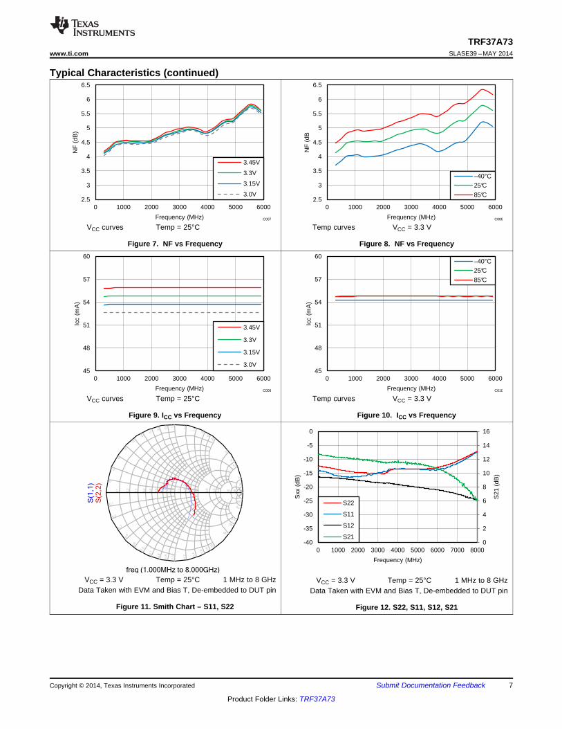
Typical Characteristics (continued)
VCC curves Temp = 25°C Temp curves VCC = 3.3 V
Figure 7. NF vs Frequency Figure 8. NF vs Frequency
VCC curves Temp = 25°C Temp curves VCC = 3.3 V
Figure 9. ICC vs Frequency Figure 10. ICC vs Frequency
VCC = 3.3 V Temp = 25°C 1 MHz to 8 GHz VCC = 3.3 V Temp = 25°C 1 MHz to 8 GHzData Taken with EVM and Bias T, De-embedded to DUT pin Data Taken with EVM and Bias T, De-embedded to DUT pin
Figure 11. Smith Chart – S11, S22 Figure 12. S22, S11, S12, S21
Copyright © 2014, Texas Instruments Incorporated Submit Documentation Feedback 7
Product Folder Links: TRF37A73

Inp
ut
Ma
tch
Ou
tpu
t
Ma
tch
Active Bias and
Temperature
Compensation
VCC VCC
Power Down
RF Input RF Output
TRF37A73SLASE39 –MAY 2014 www.ti.com
7 Detailed Description
7.1 OverviewThe device is a 3.3 V general purpose RF gain block. It is a SiGe Darlington amplifier with integrated 50 Ω inputand output matching. The device contains an active bias circuit to maintain performance over a wide temperatureand voltage range. The included power down function allows the amplifier to shut down saving power when theamplifier is not needed. Fast shut down and start up enable the amplifier to be used in a host of time divisionduplex applications.
7.2 Functional Block Diagram
7.3 Feature Description
The TRF37A73 is a fixed gain RF amplifier. It is internally matched to 50 Ω on both the input and output. It is afully cascadable general purpose amplifier. The included active bias circuitry ensures the amplifier performanceis optimized over the full operating temperature and voltage ranges.
7.4 Device Functional Modes
7.4.1 Power DownThe TRF37A73 PWDN pin can be left unconnected for normal operation or a logic-high for disable modeoperation. For applications that use the power down mode, normal 5 V TLL levels are supported.
8 Submit Documentation Feedback Copyright © 2014, Texas Instruments Incorporated
Product Folder Links: TRF37A73

1
2
3
4
VCC
RFIN
8
7
6
5
RFOUT
C5
C2C1
DC Blocking Capacitor
DC Blocking Capacitor
RF Choke Inductor
DC Bypass Capacitor
RF Bypass Capacitors
RF In RF Out
VCC
C3
C4
L1
PWDN
TRF37A73www.ti.com SLASE39 –MAY 2014
8 Applications and Implementation
8.1 Application InformationThe TRF37A73 is a wideband, high performance, general purpose RF amplifier. To maximize its performance,good RF layout and grounding techniques should be employed.
8.2 Typical ApplicationThe TRF37A73 device is typically placed in a system as illustrated in Figure 13.
Figure 13. Typical Application Schematic for TRF37A73
8.2.1 Design Requirements
Table 1. Design ParametersPARAMETERS EXAMPLE VALUES
Input power range < 3 dBmOutput power < 18 dBm
Operating frequency range 1 — 6000 MHz
Copyright © 2014, Texas Instruments Incorporated Submit Documentation Feedback 9
Product Folder Links: TRF37A73
0
2
4
6
8
10
12
14
16
18
20
22
0
2
4
6
8
10
12
14
16
18
20
22
0 1000 2000 3000 4000 5000 6000
NF
(dB
)
OP
1dB
(d
Bm
)
Frequency (MHz)
OP1dB
NF
C017
TRF37A73SLASE39 –MAY 2014 www.ti.com
8.2.2 Detailed Design Procedure
The TRF37A73 is a simple to use internally matched and cascadable RF amplifier. Following the recommendedRF layout with good quality RF components and local DC bypass capacitors will ensure optimal performance isachieved. TI provides various support materials including S-Parameter and ADS models to allow the design to beoptimized to the user's particular performance needs.
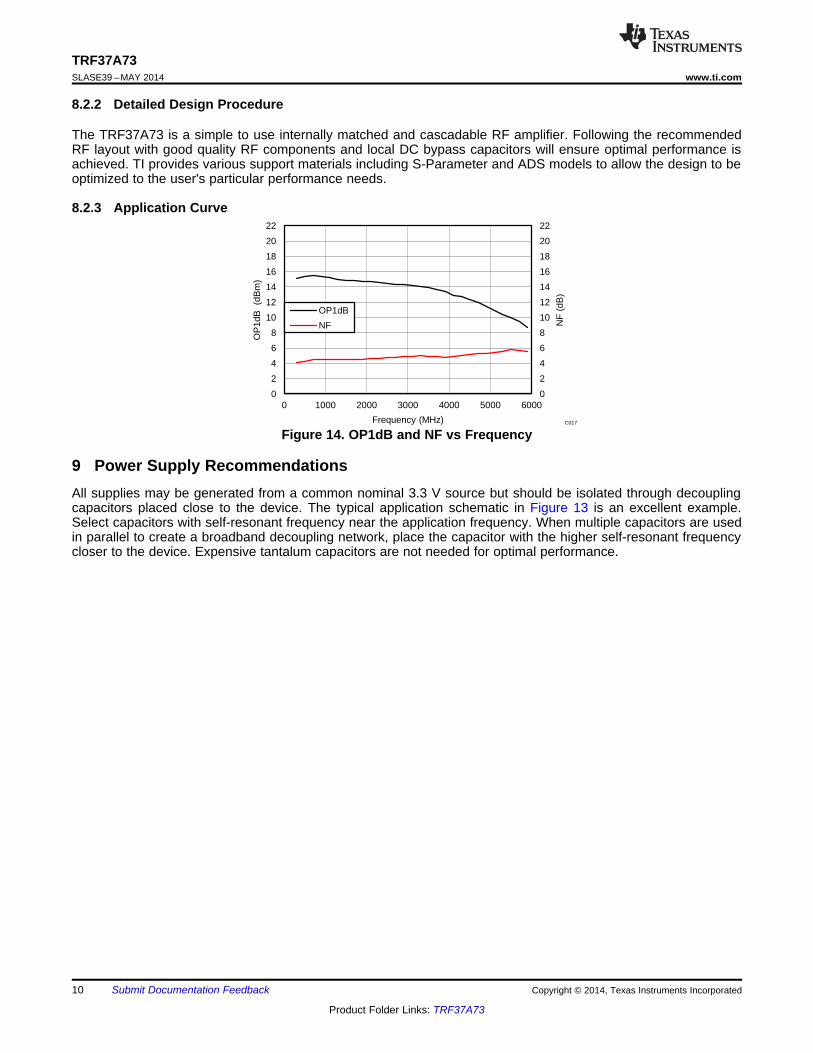
8.2.3 Application Curve
Figure 14. OP1dB and NF vs Frequency
9 Power Supply RecommendationsAll supplies may be generated from a common nominal 3.3 V source but should be isolated through decouplingcapacitors placed close to the device. The typical application schematic in Figure 13 is an excellent example.Select capacitors with self-resonant frequency near the application frequency. When multiple capacitors are usedin parallel to create a broadband decoupling network, place the capacitor with the higher self-resonant frequencycloser to the device. Expensive tantalum capacitors are not needed for optimal performance.
10 Submit Documentation Feedback Copyright © 2014, Texas Instruments Incorporated
Product Folder Links: TRF37A73

11
22
33
44
VCC
NC
NC
RFIN
88
77
66
55
NC
PWDN
RFOUT
NC
DC Blocking Capacitor
DC Blocking Capacitor
RF Choke Inductor
DC Bypass Capacitor
DC Bypass Capacitor
RF Bypass Capacitors
RF In RF Out
VCC
Note: Ensure good RF microstrip or stripline traces are used to connect the external components to the RF input and output pins
Note: Ensure all components are connected to a common RF/DC ground plane with plenty of vias
Note: Single DC bypass capacitor can be used as long as it is close to the pin 1 and is tied to the common ground plane
TRF37A73www.ti.com SLASE39 –MAY 2014
10 Layout
10.1 Layout GuidelinesGood layout practice helps to enable excellent linearity and isolation performance. An example of good layout isshown in Figure 15. In the example, only the top signal layer and its adjacent ground reference plane are shown.• Excellent electrical connection from the PowerPAD™ to the board ground is essential. Use the recommended
footprint, solder the pad to the board, and do not include solder mask under the pad.• Connect pad ground to device terminal ground on the top board layer.• Verify that the return DC and RF current path have a low impedance ground plane directly under the package
and RF signal traces into and out of the amplifier.• Ensure that ground planes on the top and any internal layers are well stitched with vias.• Do not route RF signal lines over breaks in the reference ground plane.• Avoid routing clocks and digital control lines near RF signal lines.• Do not route RF or DC signal lines over noisy power planes. Ground is the best reference, although clean
power planes can serve where necessary.• Place supply decoupling close to the device.
10.2 Layout Example
Figure 15. Layout
Copyright © 2014, Texas Instruments Incorporated Submit Documentation Feedback 11
Product Folder Links: TRF37A73
TRF37A73SLASE39 –MAY 2014 www.ti.com
11 Device and Documentation Support
11.1 TrademarksPowerPAD is a trademark of Texas Instruments.
11.2 Electrostatic Discharge CautionThese devices have limited built-in ESD protection. The leads should be shorted together or the device placed in conductive foamduring storage or handling to prevent electrostatic damage to the MOS gates.
11.3 GlossarySLYZ022 — TI Glossary.
This glossary lists and explains terms, acronyms and definitions.
12 Mechanical, Packaging, and Orderable InformationThe following pages include mechanical packaging and orderable information. This information is the mostcurrent data available for the designated devices. This data is subject to change without notice and revision ofthis document. For browser-based versions of this data sheet, refer to the left-hand navigation.
12 Submit Documentation Feedback Copyright © 2014, Texas Instruments Incorporated
Product Folder Links: TRF37A73

PACKAGE OPTION ADDENDUM
www.ti.com 10-Dec-2014
Addendum-Page 1
PACKAGING INFORMATION
Orderable Device Status(1)
Package Type PackageDrawing
Pins PackageQty
Eco Plan(2)
Lead/Ball Finish(6)
MSL Peak Temp(3)
Op Temp (°C) Device Marking(4/5)
Samples
TRF37A73IDSGR ACTIVE WSON DSG 8 3000 Green (RoHS& no Sb/Br)
CU NIPDAU Level-2-260C-1 YEAR -40 to 85 A73I
TRF37A73IDSGT ACTIVE WSON DSG 8 250 Green (RoHS& no Sb/Br)
CU NIPDAU Level-2-260C-1 YEAR -40 to 85 A73I
(1) The marketing status values are defined as follows:ACTIVE: Product device recommended for new designs.LIFEBUY: TI has announced that the device will be discontinued, and a lifetime-buy period is in effect.NRND: Not recommended for new designs. Device is in production to support existing customers, but TI does not recommend using this part in a new design.PREVIEW: Device has been announced but is not in production. Samples may or may not be available.OBSOLETE: TI has discontinued the production of the device.
(2) Eco Plan - The planned eco-friendly classification: Pb-Free (RoHS), Pb-Free (RoHS Exempt), or Green (RoHS & no Sb/Br) - please check http://www.ti.com/productcontent for the latest availabilityinformation and additional product content details.TBD: The Pb-Free/Green conversion plan has not been defined.Pb-Free (RoHS): TI's terms "Lead-Free" or "Pb-Free" mean semiconductor products that are compatible with the current RoHS requirements for all 6 substances, including the requirement thatlead not exceed 0.1% by weight in homogeneous materials. Where designed to be soldered at high temperatures, TI Pb-Free products are suitable for use in specified lead-free processes.Pb-Free (RoHS Exempt): This component has a RoHS exemption for either 1) lead-based flip-chip solder bumps used between the die and package, or 2) lead-based die adhesive used betweenthe die and leadframe. The component is otherwise considered Pb-Free (RoHS compatible) as defined above.Green (RoHS & no Sb/Br): TI defines "Green" to mean Pb-Free (RoHS compatible), and free of Bromine (Br) and Antimony (Sb) based flame retardants (Br or Sb do not exceed 0.1% by weightin homogeneous material)
(3) MSL, Peak Temp. - The Moisture Sensitivity Level rating according to the JEDEC industry standard classifications, and peak solder temperature.
(4) There may be additional marking, which relates to the logo, the lot trace code information, or the environmental category on the device.
(5) Multiple Device Markings will be inside parentheses. Only one Device Marking contained in parentheses and separated by a "~" will appear on a device. If a line is indented then it is a continuationof the previous line and the two combined represent the entire Device Marking for that device.
(6) Lead/Ball Finish - Orderable Devices may have multiple material finish options. Finish options are separated by a vertical ruled line. Lead/Ball Finish values may wrap to two lines if the finishvalue exceeds the maximum column width.
Important Information and Disclaimer:The information provided on this page represents TI's knowledge and belief as of the date that it is provided. TI bases its knowledge and belief on informationprovided by third parties, and makes no representation or warranty as to the accuracy of such information. Efforts are underway to better integrate information from third parties. TI has taken andcontinues to take reasonable steps to provide representative and accurate information but may not have conducted destructive testing or chemical analysis on incoming materials and chemicals.TI and TI suppliers consider certain information to be proprietary, and thus CAS numbers and other limited information may not be available for release.

PACKAGE OPTION ADDENDUM
www.ti.com 10-Dec-2014
Addendum-Page 2
In no event shall TI's liability arising out of such information exceed the total purchase price of the TI part(s) at issue in this document sold by TI to Customer on an annual basis.

TAPE AND REEL INFORMATION
*All dimensions are nominal
Device PackageType
PackageDrawing
Pins SPQ ReelDiameter
(mm)
ReelWidth
W1 (mm)
A0(mm)
B0(mm)
K0(mm)
P1(mm)
W(mm)
Pin1Quadrant
TRF37A73IDSGR WSON DSG 8 3000 180.0 8.4 2.3 2.3 1.15 4.0 8.0 Q2
TRF37A73IDSGT WSON DSG 8 250 180.0 8.4 2.3 2.3 1.15 4.0 8.0 Q2
PACKAGE MATERIALS INFORMATION
www.ti.com 11-Dec-2014
Pack Materials-Page 1

*All dimensions are nominal
Device Package Type Package Drawing Pins SPQ Length (mm) Width (mm) Height (mm)
TRF37A73IDSGR WSON DSG 8 3000 210.0 185.0 35.0
TRF37A73IDSGT WSON DSG 8 250 210.0 185.0 35.0
PACKAGE MATERIALS INFORMATION
www.ti.com 11-Dec-2014
Pack Materials-Page 2

www.ti.com
PACKAGE OUTLINE
C
SEE OPTIONALTERMINAL 8X 0.3
0.2
1.6 0.12X1.5
0.9 0.1
6X 0.5
8X 0.40.2
0.050.00
0.8 MAX
A 2.11.9
B
2.11.9
0.30.2
0.40.2
(0.2) TYP
WSON - 0.8 mm max heightDSG0008APLASTIC SMALL OUTLINE - NO LEAD
4218900/B 09/2017
PIN 1 INDEX AREA
SEATING PLANE
0.08 C
1
4 5
8
PIN 1 ID0.1 C A B0.05 C
THERMAL PADEXPOSED
9
NOTES: 1. All linear dimensions are in millimeters. Any dimensions in parenthesis are for reference only. Dimensioning and tolerancing per ASME Y14.5M. 2. This drawing is subject to change without notice. 3. The package thermal pad must be soldered to the printed circuit board for thermal and mechanical performance.
SCALE 5.500
OPTIONAL TERMINALTYPICAL

www.ti.com
EXAMPLE BOARD LAYOUT
0.07 MINALL AROUND
0.07 MAXALL AROUND
8X (0.25)
(1.6)
(1.9)
6X (0.5)
(0.9) ( 0.2) VIATYP
(0.55)
8X (0.5)
(R0.05) TYP
WSON - 0.8 mm max heightDSG0008APLASTIC SMALL OUTLINE - NO LEAD
4218900/B 09/2017
SYMM
1
45
8
LAND PATTERN EXAMPLESCALE:20X
SYMM 9
NOTES: (continued) 4. This package is designed to be soldered to a thermal pad on the board. For more information, see Texas Instruments literature number SLUA271 (www.ti.com/lit/slua271).5. Vias are optional depending on application, refer to device data sheet. If any vias are implemented, refer to their locations shown on this view. It is recommended that vias under paste be filled, plugged or tented.
SOLDER MASKOPENINGSOLDER MASK
METAL UNDER
SOLDER MASKDEFINED
METALSOLDER MASKOPENING
SOLDER MASK DETAILS
NON SOLDER MASKDEFINED
(PREFERRED)
www.ti.com
EXAMPLE STENCIL DESIGN
(R0.05) TYP
8X (0.25)
8X (0.5)
(0.9)
(0.7)
(1.9)
(0.45)
6X (0.5)
WSON - 0.8 mm max heightDSG0008APLASTIC SMALL OUTLINE - NO LEAD
4218900/B 09/2017
NOTES: (continued) 6. Laser cutting apertures with trapezoidal walls and rounded corners may offer better paste release. IPC-7525 may have alternate design recommendations.
SOLDER PASTE EXAMPLEBASED ON 0.125 mm THICK STENCIL
EXPOSED PAD 9:
87% PRINTED SOLDER COVERAGE BY AREA UNDER PACKAGESCALE:25X
SYMM
1
45
8
METAL
SYMM9

IMPORTANT NOTICE
Texas Instruments Incorporated (TI) reserves the right to make corrections, enhancements, improvements and other changes to itssemiconductor products and services per JESD46, latest issue, and to discontinue any product or service per JESD48, latest issue. Buyersshould obtain the latest relevant information before placing orders and should verify that such information is current and complete.TI’s published terms of sale for semiconductor products (http://www.ti.com/sc/docs/stdterms.htm) apply to the sale of packaged integratedcircuit products that TI has qualified and released to market. Additional terms may apply to the use or sale of other types of TI products andservices.Reproduction of significant portions of TI information in TI data sheets is permissible only if reproduction is without alteration and isaccompanied by all associated warranties, conditions, limitations, and notices. TI is not responsible or liable for such reproduceddocumentation. Information of third parties may be subject to additional restrictions. Resale of TI products or services with statementsdifferent from or beyond the parameters stated by TI for that product or service voids all express and any implied warranties for theassociated TI product or service and is an unfair and deceptive business practice. TI is not responsible or liable for any such statements.Buyers and others who are developing systems that incorporate TI products (collectively, “Designers”) understand and agree that Designersremain responsible for using their independent analysis, evaluation and judgment in designing their applications and that Designers havefull and exclusive responsibility to assure the safety of Designers' applications and compliance of their applications (and of all TI productsused in or for Designers’ applications) with all applicable regulations, laws and other applicable requirements. Designer represents that, withrespect to their applications, Designer has all the necessary expertise to create and implement safeguards that (1) anticipate dangerousconsequences of failures, (2) monitor failures and their consequences, and (3) lessen the likelihood of failures that might cause harm andtake appropriate actions. Designer agrees that prior to using or distributing any applications that include TI products, Designer willthoroughly test such applications and the functionality of such TI products as used in such applications.TI’s provision of technical, application or other design advice, quality characterization, reliability data or other services or information,including, but not limited to, reference designs and materials relating to evaluation modules, (collectively, “TI Resources”) are intended toassist designers who are developing applications that incorporate TI products; by downloading, accessing or using TI Resources in anyway, Designer (individually or, if Designer is acting on behalf of a company, Designer’s company) agrees to use any particular TI Resourcesolely for this purpose and subject to the terms of this Notice.TI’s provision of TI Resources does not expand or otherwise alter TI’s applicable published warranties or warranty disclaimers for TIproducts, and no additional obligations or liabilities arise from TI providing such TI Resources. TI reserves the right to make corrections,enhancements, improvements and other changes to its TI Resources. TI has not conducted any testing other than that specificallydescribed in the published documentation for a particular TI Resource.Designer is authorized to use, copy and modify any individual TI Resource only in connection with the development of applications thatinclude the TI product(s) identified in such TI Resource. NO OTHER LICENSE, EXPRESS OR IMPLIED, BY ESTOPPEL OR OTHERWISETO ANY OTHER TI INTELLECTUAL PROPERTY RIGHT, AND NO LICENSE TO ANY TECHNOLOGY OR INTELLECTUAL PROPERTYRIGHT OF TI OR ANY THIRD PARTY IS GRANTED HEREIN, including but not limited to any patent right, copyright, mask work right, orother intellectual property right relating to any combination, machine, or process in which TI products or services are used. Informationregarding or referencing third-party products or services does not constitute a license to use such products or services, or a warranty orendorsement thereof. Use of TI Resources may require a license from a third party under the patents or other intellectual property of thethird party, or a license from TI under the patents or other intellectual property of TI.TI RESOURCES ARE PROVIDED “AS IS” AND WITH ALL FAULTS. TI DISCLAIMS ALL OTHER WARRANTIES ORREPRESENTATIONS, EXPRESS OR IMPLIED, REGARDING RESOURCES OR USE THEREOF, INCLUDING BUT NOT LIMITED TOACCURACY OR COMPLETENESS, TITLE, ANY EPIDEMIC FAILURE WARRANTY AND ANY IMPLIED WARRANTIES OFMERCHANTABILITY, FITNESS FOR A PARTICULAR PURPOSE, AND NON-INFRINGEMENT OF ANY THIRD PARTY INTELLECTUALPROPERTY RIGHTS. TI SHALL NOT BE LIABLE FOR AND SHALL NOT DEFEND OR INDEMNIFY DESIGNER AGAINST ANY CLAIM,INCLUDING BUT NOT LIMITED TO ANY INFRINGEMENT CLAIM THAT RELATES TO OR IS BASED ON ANY COMBINATION OFPRODUCTS EVEN IF DESCRIBED IN TI RESOURCES OR OTHERWISE. IN NO EVENT SHALL TI BE LIABLE FOR ANY ACTUAL,DIRECT, SPECIAL, COLLATERAL, INDIRECT, PUNITIVE, INCIDENTAL, CONSEQUENTIAL OR EXEMPLARY DAMAGES INCONNECTION WITH OR ARISING OUT OF TI RESOURCES OR USE THEREOF, AND REGARDLESS OF WHETHER TI HAS BEENADVISED OF THE POSSIBILITY OF SUCH DAMAGES.Unless TI has explicitly designated an individual product as meeting the requirements of a particular industry standard (e.g., ISO/TS 16949and ISO 26262), TI is not responsible for any failure to meet such industry standard requirements.Where TI specifically promotes products as facilitating functional safety or as compliant with industry functional safety standards, suchproducts are intended to help enable customers to design and create their own applications that meet applicable functional safety standardsand requirements. Using products in an application does not by itself establish any safety features in the application. Designers mustensure compliance with safety-related requirements and standards applicable to their applications. Designer may not use any TI products inlife-critical medical equipment unless authorized officers of the parties have executed a special contract specifically governing such use.Life-critical medical equipment is medical equipment where failure of such equipment would cause serious bodily injury or death (e.g., lifesupport, pacemakers, defibrillators, heart pumps, neurostimulators, and implantables). Such equipment includes, without limitation, allmedical devices identified by the U.S. Food and Drug Administration as Class III devices and equivalent classifications outside the U.S.TI may expressly designate certain products as completing a particular qualification (e.g., Q100, Military Grade, or Enhanced Product).Designers agree that it has the necessary expertise to select the product with the appropriate qualification designation for their applicationsand that proper product selection is at Designers’ own risk. Designers are solely responsible for compliance with all legal and regulatoryrequirements in connection with such selection.Designer will fully indemnify TI and its representatives against any damages, costs, losses, and/or liabilities arising out of Designer’s non-compliance with the terms and provisions of this Notice.
Mailing Address: Texas Instruments, Post Office Box 655303, Dallas, Texas 75265Copyright © 2017, Texas Instruments Incorporated