
Transparent Conductors and Barrier Layers for Thin Film ... · Barrier Layers for Thin Film Solar...
20
December 2001 NREL/SR-520-31379 R.G. Gordon, R. Broomhall-Dillard, X. Liu, D. Pang, and J. Barton Harvard University Cambridge, Massachusetts Transparent Conductors and Barrier Layers for Thin Film Solar Cells Final Technical Report 15 June 2001 National Renewable Energy Laboratory 1617 Cole Boulevard Golden, Colorado 80401-3393 NREL is a U.S. Department of Energy Laboratory Operated by Midwest Research Institute • Battelle • Bechtel Contract No. DE-AC36-99-GO10337
-
Upload
trinhkhuong -
Category
Documents
-
view
218 -
download
0
Transcript of Transparent Conductors and Barrier Layers for Thin Film ... · Barrier Layers for Thin Film Solar...
December 2001 � NREL/SR-520-31379
R.G. Gordon, R. Broomhall-Dillard, X. Liu,D. Pang, and J. BartonHarvard UniversityCambridge, Massachusetts
Transparent Conductors andBarrier Layers for Thin FilmSolar CellsFinal Technical Report15 June 2001
National Renewable Energy Laboratory1617 Cole BoulevardGolden, Colorado 80401-3393NREL is a U.S. Department of Energy LaboratoryOperated by Midwest Research Institute •••• Battelle •••• Bechtel
Contract No. DE-AC36-99-GO10337
December 2001 � NREL/SR-520-31379
Transparent Conductors andBarrier Layers for Thin FilmSolar CellsFinal Technical Report15 June 2001
R.G. Gordon, R. Broomhall-Dillard, X. Liu,D. Pang, and J. BartonHarvard UniversityCambridge, Massachusetts
NREL Technical Monitor: B. von RoedernPrepared under Subcontract No. XAK-8-17619-26
National Renewable Energy Laboratory1617 Cole BoulevardGolden, Colorado 80401-3393NREL is a U.S. Department of Energy LaboratoryOperated by Midwest Research Institute •••• Battelle •••• Bechtel
Contract No. DE-AC36-99-GO10337
NOTICE
This report was prepared as an account of work sponsored by an agency of the United Statesgovernment. Neither the United States government nor any agency thereof, nor any of their employees,makes any warranty, express or implied, or assumes any legal liability or responsibility for the accuracy,completeness, or usefulness of any information, apparatus, product, or process disclosed, or representsthat its use would not infringe privately owned rights. Reference herein to any specific commercialproduct, process, or service by trade name, trademark, manufacturer, or otherwise does not necessarilyconstitute or imply its endorsement, recommendation, or favoring by the United States government or anyagency thereof. The views and opinions of authors expressed herein do not necessarily state or reflectthose of the United States government or any agency thereof.
Available electronically at http://www.doe.gov/bridge
Available for a processing fee to U.S. Department of Energyand its contractors, in paper, from:
U.S. Department of EnergyOffice of Scientific and Technical InformationP.O. Box 62Oak Ridge, TN 37831-0062phone: 865.576.8401fax: 865.576.5728email: [email protected]
Available for sale to the public, in paper, from:U.S. Department of CommerceNational Technical Information Service5285 Port Royal RoadSpringfield, VA 22161phone: 800.553.6847fax: 703.605.6900email: [email protected] ordering: http://www.ntis.gov/ordering.htm
Printed on paper containing at least 50% wastepaper, including 20% postconsumer waste
iii
Contents
Executive Summary .................................................................................................................................... 1
Background, Approaches Taken, and Summary of Results ........................................................................ 2Task 1: CVD of Zinc Stannate Films and Other Buffer Layers ................................................................. 3Task 2: CVD of Fluorine-Doped Zinc Oxide Films................................................................................. 11Task 3: CVD of Aluminum Oxide Films ................................................................................................. 14References ................................................................................................................................................. 15
List of Figures
Figure 1. Diffractogram for Amorphous Zinc Stannate ............................................................................. 3Figure 2. RBS Spectrum and Simulation of Zinc-Rich Film ..................................................................... 4Figure 3. Diffractogram for Zn2SnO4 Phase............................................................................................... 4Figure 4. RBS Spectrum and Simulation of Tin-Rich Film ....................................................................... 5Figure 5. Diffractogram for Zn2SnO3 Phase............................................................................................... 5Figure 6. Zn/Sn Ratio for CVD Zinc Stannate Films Deposited from Zn(acac)2 and
Me2Sn(β-diketonates)2 ................................................................................................................ 6Figure 7. Graphical Representation of the Solar Cell Parameters using the BP Solar Buffer Layer ....... 10Figure 8. SEM of Fluorine-Doped Zinc Oxide as Deposited ................................................................... 13Figure 9. SEM of Fluorine-Doped Zinc Oxide after a 30-Second Etch in Dilute (0.1M)
Hydrochloric Acid .................................................................................................................... 14
List of Tables
Table 1. Solar Cell Parameters for Tandem Solar Cells Deposited on Zinc Stannate/ZnO:F Substrates,Compared with Cells Made on Commercial (AFG) SnO2:F in the Same Run............................. 7
Table 2. Single-Junction a-Si Solar Cells Grown on Composite Superstrates withStructure/TiO2:Nb/ZnO:F/Glass ................................................................................................... 8
Table 3. Solar Cell Parameters for Cells Made on Fluorine-Doped Zinc Oxide Covered by a ProprietaryBuffer Layer Developed by BP Solar, Compared with Cells Made on Commercial (AFG)SnO2:F. The Groups of 2 or 4 Results are for Cells Made Side-by-Side in the Same Run .......... 9
Table 4. Tandem a-Si Cell Parameters for Two Runs with Side-By Side ZnO:F and SnO2:FSuperstrates................................................................................................................................. 11
Table 5. Tandem a-Si Cell Parameters for Runs with Side-by Side ZnO:F and SnO2:F Superstrates ..... 12
1
Executive Summary
Task 1: CVD of Zinc Stannate Films and Other Buffer Layers
Amorphous silicon solar cells based on fluorine-doped zinc oxide superstrates havedemonstrated currents about 10% larger than similar cells on commonly-used fluorine-doped tinoxide. However, lower fill factors had previously negated this advantage of zinc oxide. Threedifferent buffer layers were placed between the zinc oxide and the amorphous silicon in efforts toimprove the fill factors:
1) A new CVD process was developed for making zinc stannate films with variousratios of zinc to tin. While the fill factors were improved over those of zinc oxide,they still fell short of those for standard tin oxide by a few per cent.
2) Niobium-doped titanium dioxide is highly resistant to reduction by hydrogen plasma.However, its fill factors were even lower that those without this buffer layer.
3) Cells with efficiency 10% higher than standard tin oxide were finally achieved by aproprietary buffer layer developed at BP Solar, while maintaining equal fill factors.
Task 2: CVD of Fluorine-doped Zinc Oxide Films
The CVD of highly transparent ZnO:F films was developed to provide better control of thesurface roughness and the resulting haze and light trapping. Haze values of only 4% yieldedoptimal light trapping, with currents up to 10% higher than standard tin oxide. Variations on thegrowth conditions for a-Si, such as microcrystalline p-layers and hydrogen plasma pretreatments,did not produce the consistently high fill factors made with BP Solar’s buffer layer.Larger than usual numbers of shunted cells were found among the cells made on ZnO:F.Reduction of these shunts remains a problem to be solved.
Task 3: CVD of Aluminum Oxide Films
Aluminum oxide-coated glass plates are used as substrates for deposition of fluorine-doped zincoxide for three different reasons.
1) Use of an alumina layer between soda-lime glass and fluorine-doped zinc oxide films wasfound to provide a 10% reduction in their sheet resistance. Alumina is an outstandingbarrier to diffusion of sodium. Thus it prevents contamination of the film by sodium,which traps and scatters the conduction electrons in the zinc oxide films.
2) Nucleation of fluorine-doped zinc oxide appears to be more uniform and consistent onalumina surfaces than on bare glass substrates. Thus it provides better control ofroughness and the resultant haze that is needed for efficient light-trapping in amorphoussilicon solar cells.
3) The transmission of light through the films is increased by a per cent or so becausealumina has a refractive index intermediate between that of glass and zinc oxide.
Two different liquid precursors were investigated for the CVD of alumina films:triethyldialuminum tri-sec-butoxide1 and mixed aluminum betadiketonates.2 Both of theseprecursors are now commercially available from Strem Chemical Company. Both precursorswere used successfully to make amorphous aluminum oxide films used in this project.
2
Background, Approaches Taken and Summary of Results
This research was undertaken to increase the efficiency of thin-film solar cells based onamorphous silicon in the so-called superstrate structure (glass front surface/transparentelectrically conductive oxide (TCO)/pin amorphous silicon/metal back electrode). The TCOlayer has to meet many requirements: high optical transparency in the wavelength region fromabout 350 nm to 900 nm, low electrical sheet resistance, stability during handling and depositionof the subsequent layers and during use, a textured (rough) surface to enhance optical absorptionof red and near-infrared light, and low-resistance electrical contact to the amorphous silicon p-layer. Fluorine-doped tin oxide3 has been the TCO used in most commercial superstrateamorphous silicon cells.
Fluorine-doped zinc oxide (ZnO:F) was later shown to be even more transparent than fluorine-doped tin oxide,4 as well as being more resistant to the strongly reducing conditions encounteredduring the deposition of amorphous silicon.5 Solar cells based on ZnO:F showed the expectedhigher currents, but the fill factors were lower than standard cells grown on tin oxide, resulting inno consistent improvement in efficiency. This problem was attributed to a higher electricalresistance between ZnO:F and silicon.6
One approach to decreasing the electrical resistance between ZnO:F and silicon was to insert abuffer layer between them. It seemed possible that a zinc stannate composition might combinethe best features of zinc oxide’s stability with tin oxide’s ability to form a low resistance contactto silicon.7 Under Task 1 of this contract, a process was developed for the chemical vapordeposition (CVD) of zinc stannate with various zinc/tin ratios, and solar cells were grown onthese layers. Another buffer layer that was investigated was titanium oxide, since it is also highresistant to reduction by hydrogen plasmas. Other proprietary buffer layers made at BP Solarwere also investigated, leading finally to a buffer layer that succeeded in producing lowresistance contact between silicon and ZnO:F, and cells with 10% higher efficiency than standardcells on tin oxide.
Another approach to reducing the contact resistance to ZnO:F was to modify the surfaces incontact. In Task 2, several such surface modifications were explored. Wet etching of the zincoxide surface showed some promising results in reducing the contact resistance (perhaps byproviding a clean surface), but the results were not reproducible. The wet etching also provides aready means for controllably increasing the surface roughness to any desired level, to optimizethe light-trapping. Previous work had indicated that microcrystalline p-layers could be depositedon ZnO without reduction, so solar cells with various microcystalline p-layers were made.Optimization of the p-layers did not, however, improve the efficiency of ZnO:F cells beyondthose made on tin oxide.
The optical and electrical performance of TCO layers have been known to be adversely affectedby diffusion of sodium from soda-lime glass substrates during the deposition of the TCO. Silicondioxide is the barrier material most commonly used between tin oxide and glass. In Task 3,barriers to diffusion of sodium were investigated. CVD layers of aluminum oxide were found tobe far better barriers to the diffusion of sodium. The sheet resistances of ZnO:F films werereduced by about 10% by putting an aluminum oxide film between ZnO:F and glass substrates.
3
Task 1: CVD of Zinc Stannate Films and Other Buffer Layers
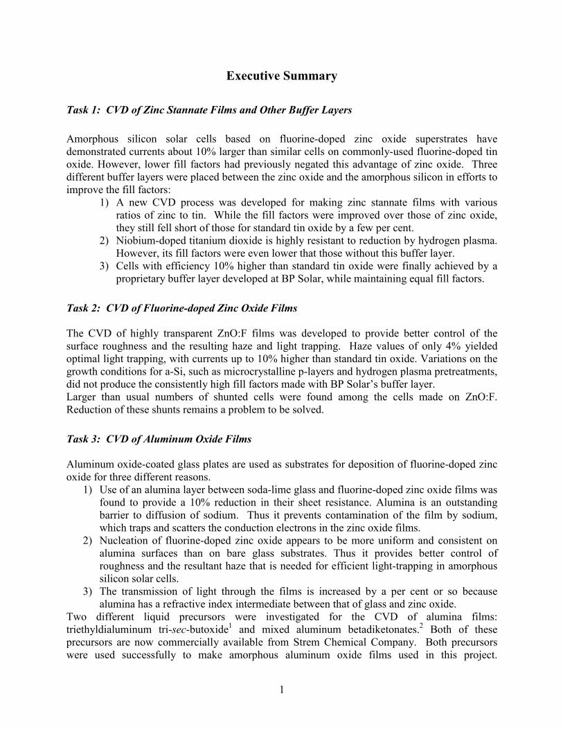
Films of zinc stannate were deposited by CVD at atmospheric pressure from a solution of theprecursors dibutyltin diacetylacetonate, Bu2Sn(acac)2, and zinc acetylacetonate, Zn(acac)2 indi(ethylene glycol)methyl ether, CH3OCH2CH2OCH2CH2OH. The reactant gas mixture wasprepared by placing such a solution in a syringe pump from which it was delivered at a steadyrate of 3 – 15 ml/hr into a Sonotek ultrasonic nozzle operated with 2.0 watts of power at 125kHz. The resulting fog was entrained into a 5-10 L/min nitrogen gas stream preheated to 220-240 oC in order to vaporize the liquid droplets. The resulting gas mixture was then mixed in a Tjoint with a 0.25-1.5 L/min stream of preheated oxygen gas (also 220-240 oC) before reachingthe inlet to the reactor. The substrates rested on a nickel plate that was electrically heated frombelow. The reactant gas mixture flowed over the substrate in a rectangular channel defined byanother nickel plate held 1 cm above the substrate by thin nickel alloy (Hastelloy C) spacers thatdefined the sides of the gas flow channel. The substrate temperature was held at 400-550 oC,while the top nickel plate was at 200-250 oC. Nearly infinite variability of Zn:Sn stoichiometryin the films was obtained by adjusting the relative precursor concentrations in solution and thedeposition parameters (e.g. O2 flow rate, substrate temperature). All as-deposited films wereamorphous by x-ray diffraction analysis (XRD). A typical spectrum is shown in Figure 1:
Figure 1: Diffractogram for Amorphous Zinc Stannate
0
20
40
60
80
100
120
140
160
30 40 50 60 70 80 90 100
2θ
Cou
nts
By annealing films of different compositions at 500 oC in air for several hours, two differentcrystalline phases were observed by XRD – one of ZnSnO3, obtained by annealing a low-zinccontent film, and one of spinel Zn2SnO4, obtained from a high-zinc content film. Annealing inair also served to remove any carbon impurity detectable by Rutherford backscattering (RBS).
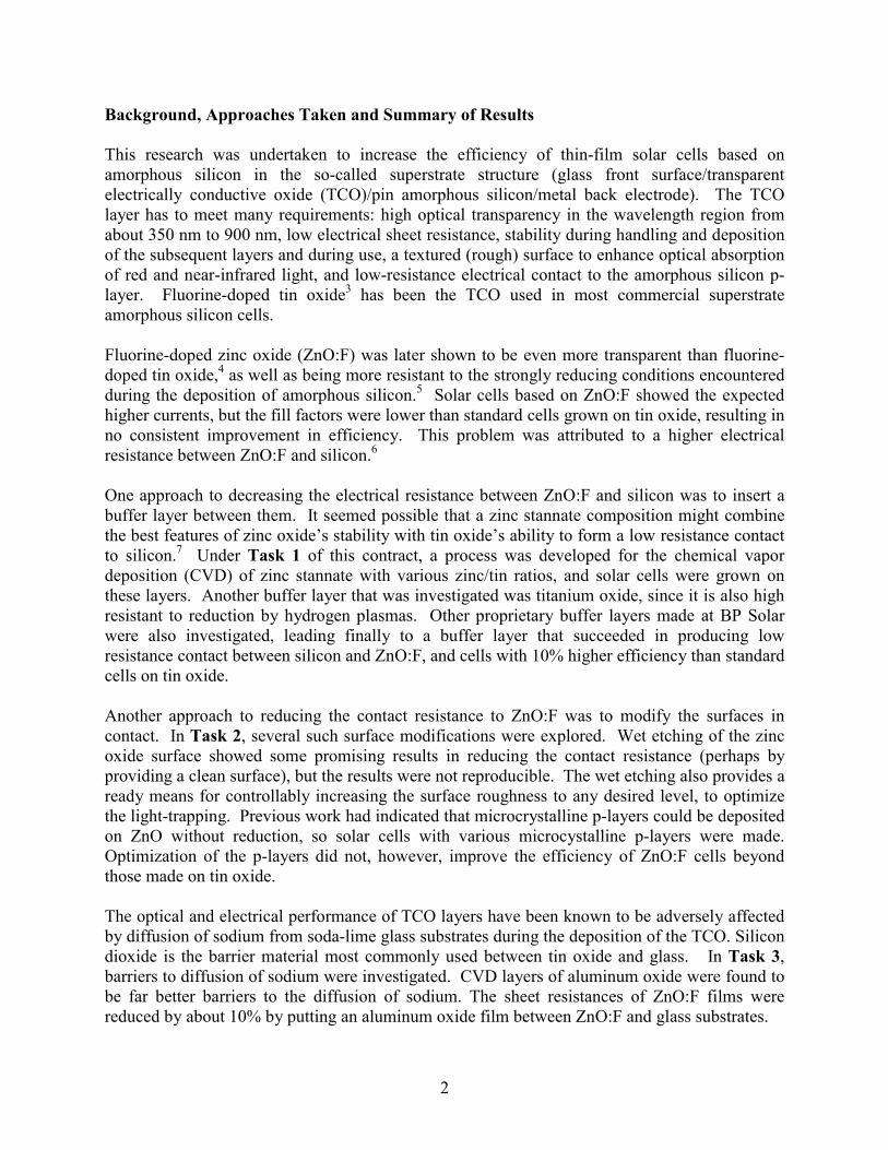
A "zinc-rich" film was obtained using a 2:1 Zn:Sn molar ratio precursor solution, usingconditions described below. The simulation of the RBS spectrum shown in Figure 2 was for a2800 Å film of composition Zn1.44SnO3.89.
4
Figure 2: RBS Spectrum and Simulation of Zinc-Rich Film
0
1000
2000
3000
4000
5000
6000
7000
0 200 400 600 800 1000Channel
Cou
nts Spectrum
Simulation
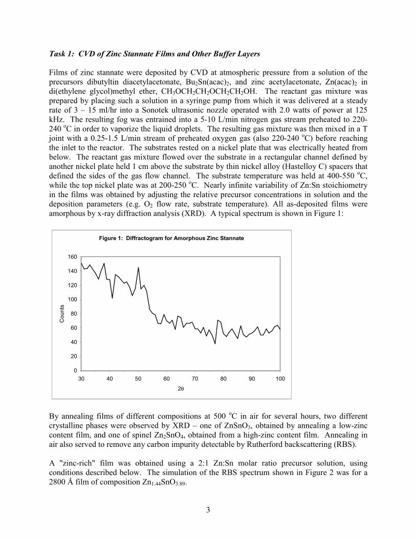
A thicker film was deposited using identical conditions, only 3.5 mL of precursor instead of0.6mL. This film was annealed at 500 oC in air for 14.3h. A spinel-type Zn2SnO4 phase8 wassubsequently detected by XRD, as shown in Figure 3:
Figure 3: Diffractogram for Zn2SnO4 Phase
0
50
100
150
200
250
30 40 50 60 70 80 90 100
2θ
Cou
nts
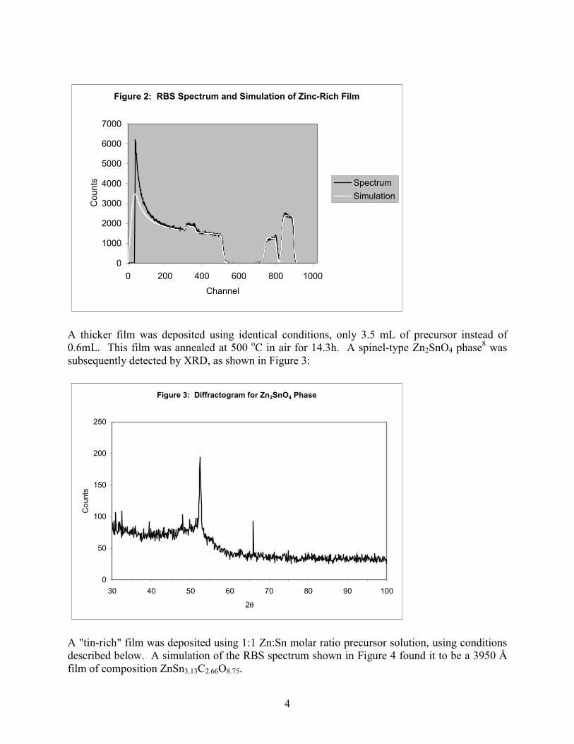
A "tin-rich" film was deposited using 1:1 Zn:Sn molar ratio precursor solution, using conditionsdescribed below. A simulation of the RBS spectrum shown in Figure 4 found it to be a 3950 Åfilm of composition ZnSn3.13C2.66O8.75.
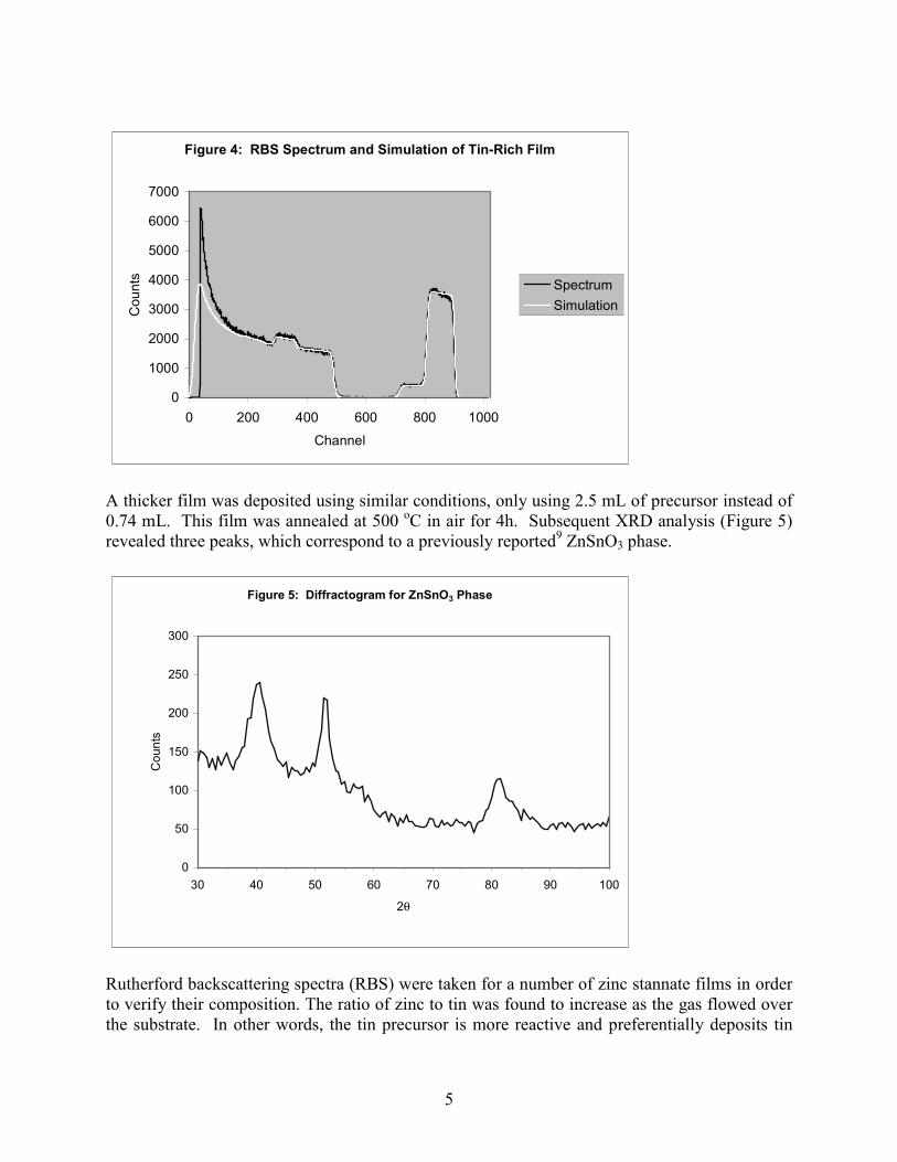
5
Figure 4: RBS Spectrum and Simulation of Tin-Rich Film
0
1000
2000
3000
4000
5000
6000
7000
0 200 400 600 800 1000Channel
Cou
nts
SpectrumSimulation
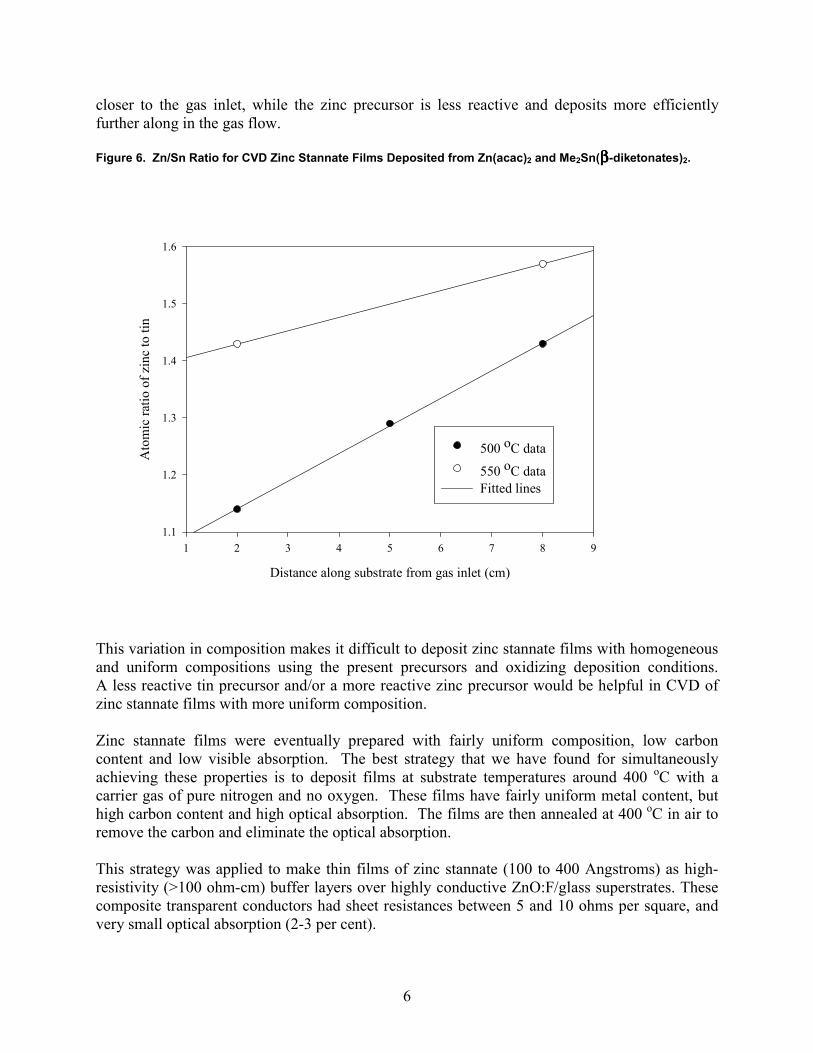
A thicker film was deposited using similar conditions, only using 2.5 mL of precursor instead of0.74 mL. This film was annealed at 500 oC in air for 4h. Subsequent XRD analysis (Figure 5)revealed three peaks, which correspond to a previously reported9 ZnSnO3 phase.
Figure 5: Diffractogram for ZnSnO3 Phase
0
50
100
150
200
250
300
30 40 50 60 70 80 90 100
2θ
Cou
nts
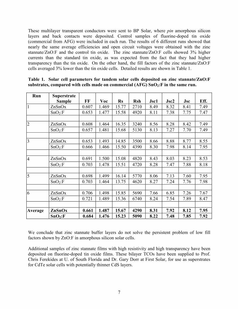
Rutherford backscattering spectra (RBS) were taken for a number of zinc stannate films in orderto verify their composition. The ratio of zinc to tin was found to increase as the gas flowed overthe substrate. In other words, the tin precursor is more reactive and preferentially deposits tin
6
closer to the gas inlet, while the zinc precursor is less reactive and deposits more efficientlyfurther along in the gas flow.
Figure 6. Zn/Sn Ratio for CVD Zinc Stannate Films Deposited from Zn(acac)2 and Me2Sn(ββββ-diketonates)2.
Distance along substrate from gas inlet (cm)
1 2 3 4 5 6 7 8 9
Ato
mic
ratio
of z
inc
to ti
n
1.1
1.2
1.3
1.4
1.5
1.6
500 oC data
550 oC dataFitted lines
This variation in composition makes it difficult to deposit zinc stannate films with homogeneousand uniform compositions using the present precursors and oxidizing deposition conditions.A less reactive tin precursor and/or a more reactive zinc precursor would be helpful in CVD ofzinc stannate films with more uniform composition.
Zinc stannate films were eventually prepared with fairly uniform composition, low carboncontent and low visible absorption. The best strategy that we have found for simultaneouslyachieving these properties is to deposit films at substrate temperatures around 400 oC with acarrier gas of pure nitrogen and no oxygen. These films have fairly uniform metal content, buthigh carbon content and high optical absorption. The films are then annealed at 400 oC in air toremove the carbon and eliminate the optical absorption.
This strategy was applied to make thin films of zinc stannate (100 to 400 Angstroms) as high-resistivity (>100 ohm-cm) buffer layers over highly conductive ZnO:F/glass superstrates. Thesecomposite transparent conductors had sheet resistances between 5 and 10 ohms per square, andvery small optical absorption (2-3 per cent).
7
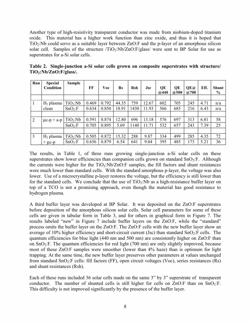
These multilayer transparent conductors were sent to BP Solar, where pin amorphous siliconlayers and back contacts were deposited. Control samples of fluorine-doped tin oxide(commercial from AFG) were included in each run. The results of 6 different runs showed thatnearly the same average efficiencies and open circuit voltages were obtained with the zincstannate/ZnO:F and the control tin oxide. The zinc stannate/ZnO:F cells showed 3% highercurrents than the standard tin oxide, as was expected from the fact that they had highertransparency than the tin oxide. On the other hand, the fill factors of the zinc stannate/ZnO:Fcells averaged 3% lower than the tin oxide cells. Detailed results are shown in Table 1.
Table 1. Solar cell parameters for tandem solar cells deposited on zinc stannate/ZnO:Fsubstrates, compared with cells made on commercial (AFG) SnO2:F in the same run.
Run SuperstrateSample FF Voc Rs Rsh Jsc1 Jsc2 Jsc Eff.
1 ZnSnOx 0.607 1.469 15.77 2710 8.49 8.32 8.41 7.49SnO2:F 0.653 1.477 15.58 4920 8.11 7.38 7.75 7.47
2 ZnSnOx 0.608 1.464 16.35 3240 8.56 8.28 8.42 7.49SnO2:F 0.657 1.481 15.68 5130 8.13 7.27 7.70 7.49
3 ZnSnOx 0.653 1.493 14.85 3500 8.66 8.88 8.77 8.55SnO2:F 0.666 1.466 15.50 4390 8.30 7.98 8.14 7.95
4 ZnSnOx 0.691 1.500 15.08 4820 8.43 8.03 8.23 8.53SnO2:F 0.703 1.478 15.51 4720 8.28 7.47 7.88 8.18
5 ZnSnOx 0.698 1.499 16.14 5770 8.06 7.13 7.60 7.95SnO2:F 0.703 1.464 13.75 4620 8.27 7.24 7.76 7.98
6 ZnSnOx 0.706 1.498 15.85 5690 7.66 6.85 7.26 7.67SnO2:F 0.721 1.489 15.36 6740 8.24 7.54 7.89 8.47
Average ZnSnOx 0.661 1.487 15.67 4290 8.31 7.92 8.12 7.95SnO2:F 0.684 1.476 15.23 5090 8.22 7.48 7.85 7.92
We conclude that zinc stannate buffer layers do not solve the persistent problem of low fillfactors shown by ZnO:F in amorphous silicon solar cells.
Additional samples of zinc stannate films with high resistivity and high transparency have beendeposited on fluorine-doped tin oxide films. These bilayer TCOs have been supplied to Prof.Chris Ferekides at U. of South Florida and Dr. Gary Dorr at First Solar, for use as superstratesfor CdTe solar cells with potentially thinner CdS layers.
8
Another type of high-resistivity transparent conductor was made from niobium-doped titaniumoxide. This material has a higher work function than zinc oxide, and thus it is hoped thatTiO2:Nb could serve as a suitable layer between ZnO:F and the p-layer of an amorphous siliconsolar cell. Samples of the structure /TiO2:Nb/ZnO:F/glass/ were sent to BP Solar for use assuperstrates for a-Si solar cells.
Table 2. Single-junction a-Si solar cells grown on composite superstrates with structure/TiO2:Nb/ZnO:F/glass/.
Run SpecialCondition
SampleFF Voc Rs Rsh Jsc QE
@440QE
@500QE@@700
Eff. Shunt%
1 H2 plasma TiO2:Nb 0.469 0.792 44.35 759 12.67 602 705 245 4.71 n/aclean SnO2:F 0.634 0.850 18.91 1430 11.93 566 685 216 6.43 n/a
2 µc-p + a-p TiO2:Nb 0.591 0.874 12.80 696 13.18 576 697 313 6.81 58SnO2:F 0.705 0.895 5.69 1140 11.71 532 657 243 7.39 25
3 H2 plasma TiO2:Nb 0.505 0.872 15.32 288 9.87 334 499 285 4.35 72+ µc-p SnO2:F 0.656 0.879 6.54 641 9.04 395 485 173 5.21 36
The results, in Table 1, of three runs growing single-junction a-Si solar cells on thesesuperstrates show lower efficiencies than companion cells grown on standard SnO2:F. Althoughthe currents were higher for the TiO2:Nb/ZnO:F samples, the fill factors and shunt resistanceswere much lower than standard cells. With the standard amorphous p-layer, the voltage was alsolower. Use of a microcrystalline p-layer restores the voltage, but the efficiency is still lower thanfor the standard cells. We conclude that the use of TiO2:Nb as a high-resistance buffer layer ontop of a TCO is not a promising approach, even though the material has good resistance tohydrogen plasma.
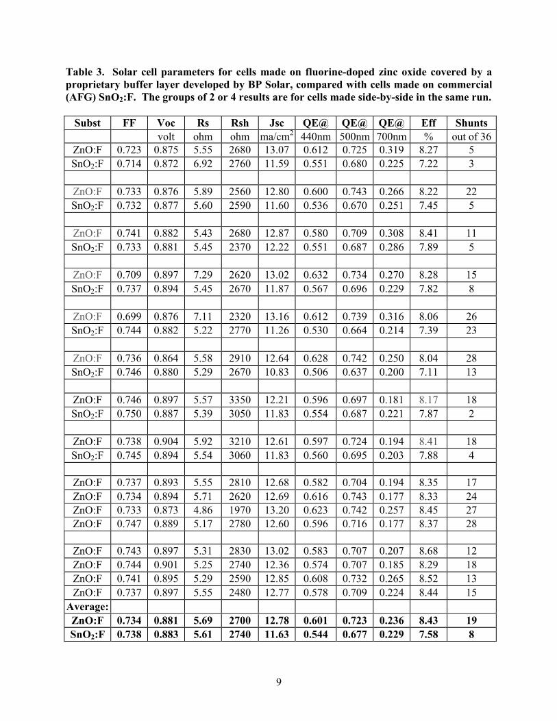
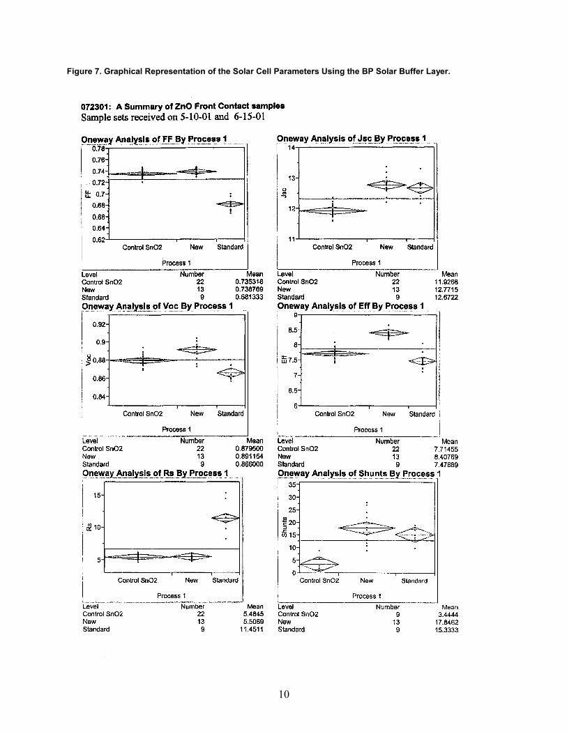
A third buffer layer was developed at BP Solar. It was deposited on the ZnO:F superstratesbefore deposition of the amorphous silicon solar cells. Solar cell parameters for some of thesecells are given in tabular form in Table 3, and for others in graphical form in Figure 7. Theresults labeled “new” in Figure 7 include buffer layers on the ZnO:F, while the “standard”process omits the buffer layer on the ZnO:F. The ZnO:F cells with the new buffer layer show anaverage of 10% higher efficiency and short-circuit current (Jsc) than standard SnO2:F cells. Thequantum efficiencies for blue light (440 nm and 500 nm) are consistently higher on ZnO:F thanon SnO2:F. The quantum efficiencies for red light (700 nm) are only slightly improved, becausemost of these ZnO:F samples were smoother (lower than 4% haze) than is optimum for lighttrapping. At the same time, the new buffer layer preserves other parameters at values unchangedfrom standard SnO2:F cells: fill factors (FF), open circuit voltages (Voc), series resistances (Rs)and shunt resistances (Rsh).
Each of these runs included 36 solar cells made on the same 3” by 3” superstrate of transparentconductor. The number of shunted cells is still higher for cells on ZnO:F than on SnO2:F.This difficulty is not improved significantly by the presence of the buffer layer.
9
Table 3. Solar cell parameters for cells made on fluorine-doped zinc oxide covered by aproprietary buffer layer developed by BP Solar, compared with cells made on commercial(AFG) SnO2:F. The groups of 2 or 4 results are for cells made side-by-side in the same run.
Subst FF Voc Rs Rsh Jsc QE@ QE@ QE@ Eff Shuntsvolt ohm ohm ma/cm2 440nm 500nm 700nm % out of 36
ZnO:F 0.723 0.875 5.55 2680 13.07 0.612 0.725 0.319 8.27 5SnO2:F 0.714 0.872 6.92 2760 11.59 0.551 0.680 0.225 7.22 3
ZnO:F 0.733 0.876 5.89 2560 12.80 0.600 0.743 0.266 8.22 22SnO2:F 0.732 0.877 5.60 2590 11.60 0.536 0.670 0.251 7.45 5
ZnO:F 0.741 0.882 5.43 2680 12.87 0.580 0.709 0.308 8.41 11SnO2:F 0.733 0.881 5.45 2370 12.22 0.551 0.687 0.286 7.89 5
ZnO:F 0.709 0.897 7.29 2620 13.02 0.632 0.734 0.270 8.28 15SnO2:F 0.737 0.894 5.45 2670 11.87 0.567 0.696 0.229 7.82 8
ZnO:F 0.699 0.876 7.11 2320 13.16 0.612 0.739 0.316 8.06 26SnO2:F 0.744 0.882 5.22 2770 11.26 0.530 0.664 0.214 7.39 23
ZnO:F 0.736 0.864 5.58 2910 12.64 0.628 0.742 0.250 8.04 28SnO2:F 0.746 0.880 5.29 2670 10.83 0.506 0.637 0.200 7.11 13
ZnO:F 0.746 0.897 5.57 3350 12.21 0.596 0.697 0.181 8.17 18SnO2:F 0.750 0.887 5.39 3050 11.83 0.554 0.687 0.221 7.87 2
ZnO:F 0.738 0.904 5.92 3210 12.61 0.597 0.724 0.194 8.41 18SnO2:F 0.745 0.894 5.54 3060 11.83 0.560 0.695 0.203 7.88 4
ZnO:F 0.737 0.893 5.55 2810 12.68 0.582 0.704 0.194 8.35 17ZnO:F 0.734 0.894 5.71 2620 12.69 0.616 0.743 0.177 8.33 24ZnO:F 0.733 0.873 4.86 1970 13.20 0.623 0.742 0.257 8.45 27ZnO:F 0.747 0.889 5.17 2780 12.60 0.596 0.716 0.177 8.37 28
ZnO:F 0.743 0.897 5.31 2830 13.02 0.583 0.707 0.207 8.68 12ZnO:F 0.744 0.901 5.25 2740 12.36 0.574 0.707 0.185 8.29 18ZnO:F 0.741 0.895 5.29 2590 12.85 0.608 0.732 0.265 8.52 13ZnO:F 0.737 0.897 5.55 2480 12.77 0.578 0.709 0.224 8.44 15
Average:ZnO:F 0.734 0.881 5.69 2700 12.78 0.601 0.723 0.236 8.43 19SnO2:F 0.738 0.883 5.61 2740 11.63 0.544 0.677 0.229 7.58 8
10
Figure 7. Graphical Representation of the Solar Cell Parameters Using the BP Solar Buffer Layer.
11
Task 2: CVD of Fluorine-Doped Zinc Oxide Films
Zinc acetylacetonate, an inexpensive and commercially available material was used successfullyfor depositing zinc oxide films. Extensive tests of several fluorine-containing materials aspotential fluorine dopants, failed to increase the conductivity of zinc oxide films deposited fromzinc acetylacetonate. Thus the tetramethylethylenediamine adduct of diethylzinc along with theeffective fluorine dopant benzoyl fluoride, is still the best way to deposit highly conductive andtransparent fluorine-doped zinc oxide.10
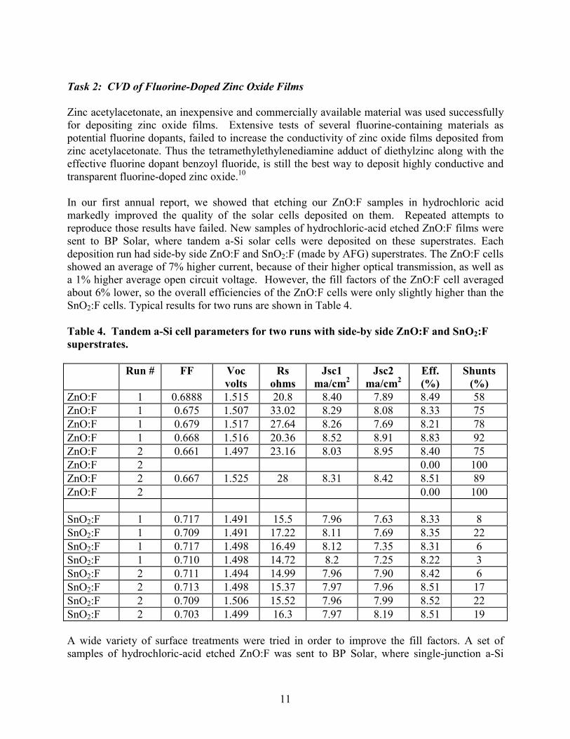
In our first annual report, we showed that etching our ZnO:F samples in hydrochloric acidmarkedly improved the quality of the solar cells deposited on them. Repeated attempts toreproduce those results have failed. New samples of hydrochloric-acid etched ZnO:F films weresent to BP Solar, where tandem a-Si solar cells were deposited on these superstrates. Eachdeposition run had side-by side ZnO:F and SnO2:F (made by AFG) superstrates. The ZnO:F cellsshowed an average of 7% higher current, because of their higher optical transmission, as well asa 1% higher average open circuit voltage. However, the fill factors of the ZnO:F cell averagedabout 6% lower, so the overall efficiencies of the ZnO:F cells were only slightly higher than theSnO2:F cells. Typical results for two runs are shown in Table 4.
Table 4. Tandem a-Si cell parameters for two runs with side-by side ZnO:F and SnO2:Fsuperstrates.
Run # FF Vocvolts
Rsohms
Jsc1ma/cm2
Jsc2ma/cm2
Eff.(%)
Shunts(%)
ZnO:F 1 0.6888 1.515 20.8 8.40 7.89 8.49 58ZnO:F 1 0.675 1.507 33.02 8.29 8.08 8.33 75ZnO:F 1 0.679 1.517 27.64 8.26 7.69 8.21 78ZnO:F 1 0.668 1.516 20.36 8.52 8.91 8.83 92ZnO:F 2 0.661 1.497 23.16 8.03 8.95 8.40 75ZnO:F 2 0.00 100ZnO:F 2 0.667 1.525 28 8.31 8.42 8.51 89ZnO:F 2 0.00 100
SnO2:F 1 0.717 1.491 15.5 7.96 7.63 8.33 8SnO2:F 1 0.709 1.491 17.22 8.11 7.69 8.35 22SnO2:F 1 0.717 1.498 16.49 8.12 7.35 8.31 6SnO2:F 1 0.710 1.498 14.72 8.2 7.25 8.22 3SnO2:F 2 0.711 1.494 14.99 7.96 7.90 8.42 6SnO2:F 2 0.713 1.498 15.37 7.97 7.96 8.51 17SnO2:F 2 0.709 1.506 15.52 7.96 7.99 8.52 22SnO2:F 2 0.703 1.499 16.3 7.97 8.19 8.51 19
A wide variety of surface treatments were tried in order to improve the fill factors. A set ofsamples of hydrochloric-acid etched ZnO:F was sent to BP Solar, where single-junction a-Si
12
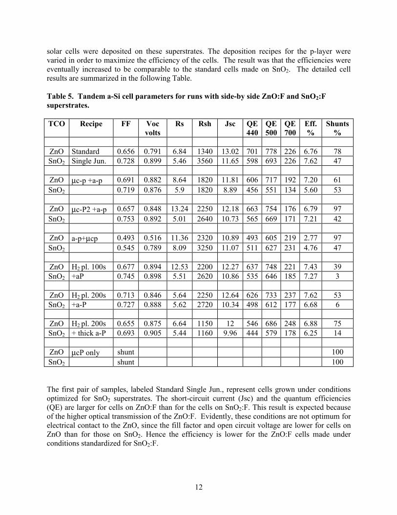
solar cells were deposited on these superstrates. The deposition recipes for the p-layer werevaried in order to maximize the efficiency of the cells. The result was that the efficiencies wereeventually increased to be comparable to the standard cells made on SnO2. The detailed cellresults are summarized in the following Table.
Table 5. Tandem a-Si cell parameters for runs with side-by side ZnO:F and SnO2:Fsuperstrates.
TCO Recipe FF Vocvolts
Rs Rsh Jsc QE440
QE500
QE700
Eff.%
Shunts%
ZnO Standard 0.656 0.791 6.84 1340 13.02 701 778 226 6.76 78SnO2 Single Jun. 0.728 0.899 5.46 3560 11.65 598 693 226 7.62 47
ZnO µc-p +a-p 0.691 0.882 8.64 1820 11.81 606 717 192 7.20 61SnO2 0.719 0.876 5.9 1820 8.89 456 551 134 5.60 53
ZnO µc-P2 +a-p 0.657 0.848 13.24 2250 12.18 663 754 176 6.79 97SnO2 0.753 0.892 5.01 2640 10.73 565 669 171 7.21 42
ZnO a-p+µcp 0.493 0.516 11.36 2320 10.89 493 605 219 2.77 97SnO2 0.545 0.789 8.09 3250 11.07 511 627 231 4.76 47
ZnO H2 pl. 100s 0.677 0.894 12.53 2200 12.27 637 748 221 7.43 39SnO2 +aP 0.745 0.898 5.51 2620 10.86 535 646 185 7.27 3
ZnO H2 pl. 200s 0.713 0.846 5.64 2250 12.64 626 733 237 7.62 53SnO2 +a-P 0.727 0.888 5.62 2720 10.34 498 612 177 6.68 6
ZnO H2 pl. 200s 0.655 0.875 6.64 1150 12 546 686 248 6.88 75SnO2 + thick a-P 0.693 0.905 5.44 1160 9.96 444 579 178 6.25 14
ZnO µcP only shunt 100SnO2 shunt 100
The first pair of samples, labeled Standard Single Jun., represent cells grown under conditionsoptimized for SnO2 superstrates. The short-circuit current (Jsc) and the quantum efficiencies(QE) are larger for cells on ZnO:F than for the cells on SnO2:F. This result is expected becauseof the higher optical transmission of the ZnO:F. Evidently, these conditions are not optimum forelectrical contact to the ZnO, since the fill factor and open circuit voltage are lower for cells onZnO than for those on SnO2. Hence the efficiency is lower for the ZnO:F cells made underconditions standardized for SnO2:F.
13
The next run inserted a micro-crystalline p-layer (µc-p) prior to the usual amorphous p-layer(a-p). This resulted in improving the fill factor, voltage and efficiency of the ZnO:F cells tovalues close to, but still slightly below, those of the standard cells. A second micro-crystallinerecipe (µc-p2) was less successful. Reversing the order of the µc-p and a-p layers producedterrible results, as expected.
The next three runs introduced a hydrogen plasma clean prior to deposition of the standardamorphous p-layer. A 200 second hydrogen plasma clean improved the efficiency of the ZnO:Fcells made with the standard recipe up to values equal to those of the standard SnO2:F cells.The same hydrogen plasma clean significantly degraded the currents of the SnO2:F cells,probably by causing reduction of the tin oxide and consequent lowering of the opticaltransmission. As expected, the zinc oxide was not reduced by the plasma clean.
Many solar cells deposited on the ZnO:F superstrates were shunted, while adjacent superstratesof SnO2:F showed much smaller “normal” numbers of shunts. Table 1 gives some typical resultsfor numbers of shunts. On some ZnO:F samples, all 36 cells were shunted. For example, the finalpair of samples in Table 5, made with only a µc-p layer and no a-p layer, were all shunted.
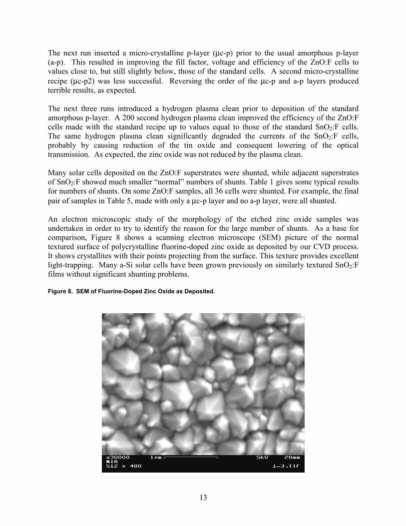
An electron microscopic study of the morphology of the etched zinc oxide samples wasundertaken in order to try to identify the reason for the large number of shunts. As a base forcomparison, Figure 8 shows a scanning electron microscope (SEM) picture of the normaltextured surface of polycrystalline fluorine-doped zinc oxide as deposited by our CVD process.It shows crystallites with their points projecting from the surface. This texture provides excellentlight-trapping. Many a-Si solar cells have been grown previously on similarly textured SnO2:Ffilms without significant shunting problems.
Figure 8. SEM of Fluorine-Doped Zinc Oxide as Deposited.
14
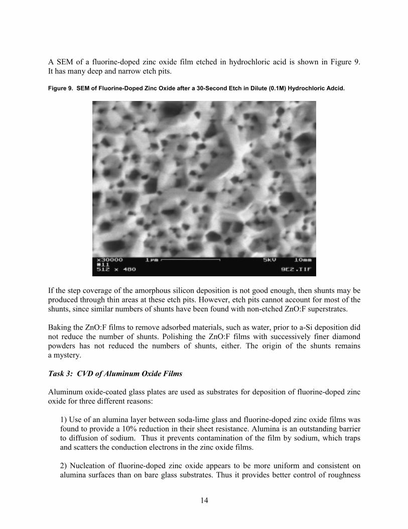
A SEM of a fluorine-doped zinc oxide film etched in hydrochloric acid is shown in Figure 9.It has many deep and narrow etch pits.
Figure 9. SEM of Fluorine-Doped Zinc Oxide after a 30-Second Etch in Dilute (0.1M) Hydrochloric Adcid.
If the step coverage of the amorphous silicon deposition is not good enough, then shunts may beproduced through thin areas at these etch pits. However, etch pits cannot account for most of theshunts, since similar numbers of shunts have been found with non-etched ZnO:F superstrates.
Baking the ZnO:F films to remove adsorbed materials, such as water, prior to a-Si deposition didnot reduce the number of shunts. Polishing the ZnO:F films with successively finer diamondpowders has not reduced the numbers of shunts, either. The origin of the shunts remainsa mystery.
Task 3: CVD of Aluminum Oxide Films
Aluminum oxide-coated glass plates are used as substrates for deposition of fluorine-doped zincoxide for three different reasons:
1) Use of an alumina layer between soda-lime glass and fluorine-doped zinc oxide films wasfound to provide a 10% reduction in their sheet resistance. Alumina is an outstanding barrierto diffusion of sodium. Thus it prevents contamination of the film by sodium, which trapsand scatters the conduction electrons in the zinc oxide films.
2) Nucleation of fluorine-doped zinc oxide appears to be more uniform and consistent onalumina surfaces than on bare glass substrates. Thus it provides better control of roughness
15
and the resultant haze that is needed for efficient light-trapping in amorphous siliconsolar cells.
3) The transmission of light through the films is increased by a per cent or so becausealumina has a refractive index intermediate between that of glass and zinc oxide.
Two different liquid precursors were investigated for the CVD of alumina films:triethyldialuminum tri-sec-butoxide1 and mixed aluminum betadiketonates.2 Both of theseprecursors are now commercially available from Strem Chemical Company, Newburyport, MA.Both precursors were used successfully to make amorphous aluminum oxide films used inthis project.
References
1 Roy G. Gordon, Keith Kramer and Xinye Liu, Materials Res. Soc. Proc. 446, 383 (1997);Roy G. Gordon, Keith Kramer and Xinye Liu, US Patent 6,037,003 (2000).2 Roy G. Gordon, Feng Chen, Nicholas J. DiCeglie, Jr., Amos Kenigsberg, Xinye Liu, DanielTeff and John Thornton, Materials Res. Soc. Proc. 495, 63 (1998); Roy G. Gordon, US Patent6,258,157 (2001).3 R. G. Gordon, J. Proscia, F. B. Ellis, A. E. Delahoy, Solar Energy Materials 18, 263-281(1989); J. Proscia, R. G. Gordon, Thin Solid Films 214, 175-187 (1992).4 J. Hu, R. G. Gordon, Solar Cells 30, 437-450 (1991).5 S. Hegedus, H. Liang and R. G. Gordon, Amer. Inst. Phys. Conf. Proc. 353 (13th NRELPhotovoltaics Program Review, 1995), 465-72 (1996).6 Roy G. Gordon, R. Broomhall-Dillard, X. Liu, D. Pang, J. Barton, Annual Technical Report,NREL Subcontract No. XAK-8-17619-26 (2000)7 Zinc stannate buffer layers have recently been reported to increase the efficiency of CdTesuperstrate cells: X. Wu, R. Ribelin, R. G. Dhere, D. S. Albin, S. Asher, D. H. Levi, A. Mason,H. R. Moutinho, P. Shelton, Proceedings of the 28th IEEE Photovoltaic Specialists Conference(Anchorage, AK), p. 470 (2000).8 Natl. Bur. Stand. (U.S.) Monogr. 25, 1062 (1972).9 Coffeen, J. Am. Ceram. Soc. 36, 207 (1953).10 Roy G. Gordon, Keith Kramer and Haifang Liang, US Patent 6,071,561 (2000).
REPORT DOCUMENTATION PAGE Form ApprovedOMB NO. 0704-0188
Public reporting burden for this collection of information is estimated to average 1 hour per response, including the time for reviewing instructions, searching existing data sources,gathering and maintaining the data needed, and completing and reviewing the collection of information. Send comments regarding this burden estimate or any other aspect of thiscollection of information, including suggestions for reducing this burden, to Washington Headquarters Services, Directorate for Information Operations and Reports, 1215 JeffersonDavis Highway, Suite 1204, Arlington, VA 22202-4302, and to the Office of Management and Budget, Paperwork Reduction Project (0704-0188), Washington, DC 20503.
1. AGENCY USE ONLY (Leave blank) 2. REPORT DATE December, 2001
3. REPORT TYPE AND DATES COVERED Final Technical Report
15 June 20014. TITLE AND SUBTITLE Transparent Conductors and Barrier Layers for Thin Film Solar Cells, Final Technical Report, 15 June 20016. AUTHOR(S) R.G. Gordon, R. Broomhall-Dillard, X. Liu, D. Pang, and J. Barton
5. FUNDING NUMBERSCF: XAK-8-17619-26
PVP25001
7. PERFORMING ORGANIZATION NAME(S) AND ADDRESS(ES) Harvard University
Cambridge, Massachusetts
8. PERFORMING ORGANIZATIONREPORT NUMBER
9. SPONSORING/MONITORING AGENCY NAME(S) AND ADDRESS(ES)National Renewable Energy Laboratory1617 Cole Blvd.Golden, CO 80401-3393
10. SPONSORING/MONITORINGAGENCY REPORT NUMBER
NREL/SR-520-31379
11. SUPPLEMENTARY NOTES
NREL Technical Monitor: Bolko von Roedern12a. DISTRIBUTION/AVAILABILITY STATEMENT
National Technical Information ServiceU.S. Department of Commerce5285 Port Royal RoadSpringfield, VA 22161
12b. DISTRIBUTION CODE
13. ABSTRACT (Maximum 200 words) This report describes the research undertaken to increase the efficiency of thin-film solar cellsbased on amorphous silicon in the so-called �superstrate structure� (glass front surface/transparent electrically conductiveoxide (TCO)/pin amorphous silicon/metal back electrode). The TCO layer must meet many requirements: high opticaltransparency in the wavelength region from about 350 to 900 nm, low electrical sheet resistance, stability during handlingand deposition of the subsequent layers and during use, a textured (rough) surface to enhance optical absorption of redand near-infrared light, and low-resistance electrical contact to the amorphous silicon p-layer. Fluorine-doped tin oxidehas been the TCO used in most commercial superstrate amorphous silicon cells. Fluorine-doped zinc oxide (ZnO:F) waslater shown to be even more transparent than fluorine-doped tin oxide, as well as being more resistant to the stronglyreducing conditions encountered during the deposition of amorphous silicon. Solar cells based on ZnO:F showed theexpected higher currents, but the fill factors were lower than standard cells grown on tin oxide, resulting in no consistentimprovement in efficiency. This problem was recently mitigated by using a new proprietary p/buffer layer combinationdeveloped at BP Solar.
15. NUMBER OF PAGES14. SUBJECT TERMS PV; thin-film solar cells; superstrate structure; transparent conductiveoxide (TCO); fluorine-doped; proprietary buffer layer; shunted cells; precursors; hazeand light trapping 16. PRICE CODE
17. SECURITY CLASSIFICATIONOF REPORTUnclassified
18. SECURITY CLASSIFICATIONOF THIS PAGEUnclassified
19. SECURITY CLASSIFICATIONOF ABSTRACTUnclassified
20. LIMITATION OF ABSTRACT
UL
NSN 7540-01-280-5500 Standard Form 298 (Rev. 2-89)Prescribed by ANSI Std. Z39-18
298-102


