Transmitting and Receiving Multi-Channel Audio...
13
Transmitting and Receiving Multi-Channel Audio Over Frequency Modulated Radio Yanni Coroneos and Max Justicz 5/14/2015 Abstract In this paper we tackle the issue of multiple-channel radio transmission and reception with frequency modulation (FM). Specifically, we explore the aspects of FM with several channels, and the technical challenges that are faced when we transport these signals over the air. Our initial goal was to transmit our signal over a fiber-optic cable, but due to unexpected circumstances surrounding the physics of antenna transmission (discussed later), we shifted our focus to a more traditional method that operates entirely over radio. Motivation Our motivation for this project is twofold: to construct a system that is practically useful for wireless audio transmission in a home or dorm room setting, and to design a circuit that will provide us with interesting technical challenges. Radio technology fits the bill perfectly, since it is a well understood and mature technology that is notoriously difficult to implement successfully. Block Diagram Figure 1: A block diagram of our completed circuit Since our project involves transmitting and receiving, it can naturally be broken down into two major components. On the left of Figure 1, several channels of audio are modulated at distinct frequencies and mixed together using a mixing circuit. The mixed signal containing all of the information is then transmitted over an antenna to the receiving circuit. Each receiver only needs
Transcript of Transmitting and Receiving Multi-Channel Audio...

Transmitting and Receiving Multi-Channel Audio Over Frequency Modulated Radio
Yanni Coroneos and Max Justicz
5/14/2015
Abstract In this paper we tackle the issue of multiple-channel radio transmission and reception with frequency modulation (FM). Specifically, we explore the aspects of FM with several channels, and the technical challenges that are faced when we transport these signals over the air. Our initial goal was to transmit our signal over a fiber-optic cable, but due to unexpected circumstances surrounding the physics of antenna transmission (discussed later), we shifted our focus to a more traditional method that operates entirely over radio.
Motivation Our motivation for this project is twofold: to construct a system that is practically useful for wireless audio transmission in a home or dorm room setting, and to design a circuit that will provide us with interesting technical challenges. Radio technology fits the bill perfectly, since it is a well understood and mature technology that is notoriously difficult to implement successfully.
Block Diagram
Figure 1: A block diagram of our completed circuit
Since our project involves transmitting and receiving, it can naturally be broken down into two major components. On the left of Figure 1, several channels of audio are modulated at distinct frequencies and mixed together using a mixing circuit. The mixed signal containing all of the information is then transmitted over an antenna to the receiving circuit. Each receiver only needs
to tune to one modulation frequency to receive the corresponding channel of audio. In this way, if there are n inputs, there will be n outputs. Finally, the received and demodulated signal is amplified and played through a speaker.
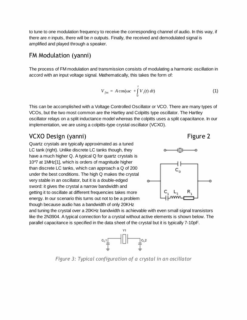
FM Modulation (yanni) The process of FM modulation and transmission consists of modulating a harmonic oscillation in accord with an input voltage signal. Mathematically, this takes the form of:
(1)A (ωc (t) dt)V fm = cos + ∫t
0V i
This can be accomplished with a Voltage Controlled Oscillator or VCO. There are many types of VCOs, but the two most common are the Hartley and Colpitts type oscillator. The Hartley oscillator relays on a split inductance model whereas the colpitts uses a split capacitance. In our implementation, we are using a colpitts-type crystal oscillator (VCXO).
VCXO Design (yanni) Figure 2 Quartz crystals are typically approximated as a tuned LC tank (right). Unlike discrete LC tanks though, they have a much higher Q. A typical Q for quartz crystals is 10 7̂ at 1MHz[1], which is orders of magnitude higher than discrete LC tanks, which can approach a Q of 200 under the best conditions. The high Q makes the crystal very stable in an oscillator, but it is a double-edged sword: it gives the crystal a narrow bandwidth and getting it to oscillate at different frequencies takes more energy. In our scenario this turns out not to be a problem though because audio has a bandwidth of only 20KHz and tuning the crystal over a 20KHz bandwidth is achievable with even small signal transistors like the 2N3904. A typical connection for a crystal without active elements is shown below. The parallel capacitance is specified in the data sheet of the crystal but it is typically 7-10pF.
Figure 3: Typical configuration of a crystal in an oscillator
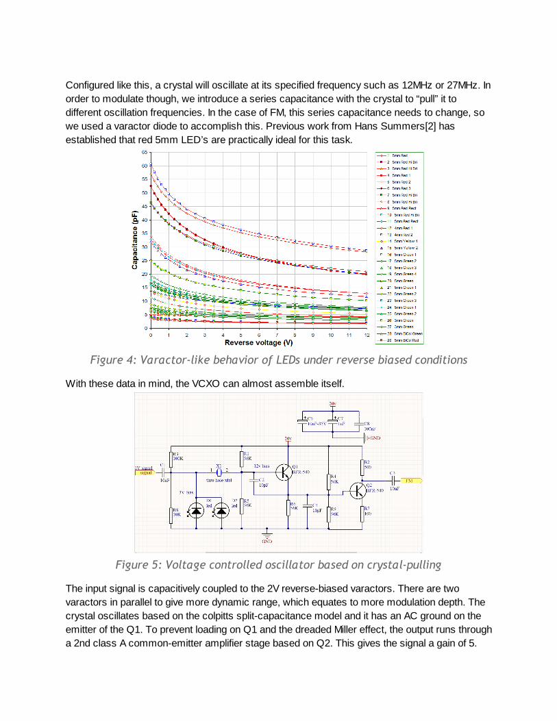
Configured like this, a crystal will oscillate at its specified frequency such as 12MHz or 27MHz. In order to modulate though, we introduce a series capacitance with the crystal to “pull” it to different oscillation frequencies. In the case of FM, this series capacitance needs to change, so we used a varactor diode to accomplish this. Previous work from Hans Summers[2] has established that red 5mm LED’s are practically ideal for this task.
Figure 4: Varactor-like behavior of LEDs under reverse biased conditions
With these data in mind, the VCXO can almost assemble itself.
Figure 5: Voltage controlled oscillator based on crystal-pulling
The input signal is capacitively coupled to the 2V reverse-biased varactors. There are two varactors in parallel to give more dynamic range, which equates to more modulation depth. The crystal oscillates based on the colpitts split-capacitance model and it has an AC ground on the emitter of the Q1. To prevent loading on Q1 and the dreaded Miller effect, the output runs through a 2nd class A common-emitter amplifier stage based on Q2. This gives the signal a gain of 5.
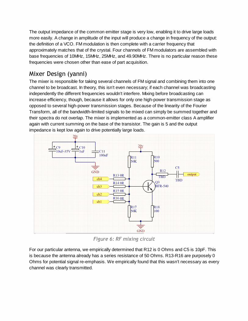
The output impedance of the common emitter stage is very low, enabling it to drive large loads more easily. A change in amplitude of the input will produce a change in frequency of the output: the definition of a VCO. FM modulation is then complete with a carrier frequency that approximately matches that of the crystal. Four channels of FM modulators are assembled with base frequencies of 10MHz, 15MHz, 25MHz, and 49.90MHz. There is no particular reason these frequencies were chosen other than ease of part acquisition.
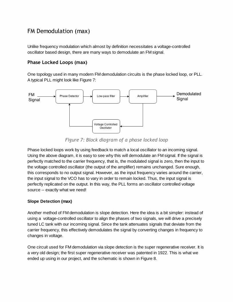
Mixer Design (yanni) The mixer is responsible for taking several channels of FM signal and combining them into one channel to be broadcast. In theory, this isn’t even necessary; if each channel was broadcasting independently the different frequencies wouldn’t interfere. Mixing before broadcasting can increase efficiency, though, because it allows for only one high-power transmission stage as opposed to several high-power transmission stages. Because of the linearity of the Fourier Transform, all of the bandwidth-limited signals to be mixed can simply be summed together and their spectra do not overlap. The mixer is implemented as a common-emitter class A amplifier again with current summing on the base of the transistor. The gain is 5 and the output impedance is kept low again to drive potentially large loads.
Figure 6: RF mixing circuit
For our particular antenna, we empirically determined that R12 is 0 Ohms and C5 is 10pF. This is because the antenna already has a series resistance of 50 Ohms. R13-R16 are purposely 0 Ohms for potential signal re-emphasis. We empirically found that this wasn’t necessary as every channel was clearly transmitted.
FM Demodulation (max) Unlike frequency modulation which almost by definition necessitates a voltage-controlled oscillator based design, there are many ways to demodulate an FM signal.
Phase Locked Loops (max) One topology used in many modern FM demodulation circuits is the phase locked loop, or PLL. A typical PLL might look like Figure 7:
Figure 7: Block diagram of a phase locked loop
Phase locked loops work by using feedback to match a local oscillator to an incoming signal. Using the above diagram, it is easy to see why this will demodulate an FM signal. If the signal is perfectly matched to the carrier frequency, that is, the modulated signal is zero, then the input to the voltage controlled oscillator (the output of the amplifier) remains unchanged. Sure enough, this corresponds to no output signal. However, as the input frequency varies around the carrier, the input signal to the VCO has to vary in order to remain locked. Thus, the input signal is perfectly replicated on the output. In this way, the PLL forms an oscillator controlled voltage source -- exactly what we need! Slope Detection (max) Another method of FM demodulation is slope detection. Here the idea is a bit simpler: instead of using a voltage-controlled oscillator to align the phases of two signals, we will drive a precisely tuned LC tank with our incoming signal. Since the tank attenuates signals that deviate from the carrier frequency, this effectively demodulates the signal by converting changes in frequency to changes in voltage. One circuit used for FM demodulation via slope detection is the super regenerative receiver. It is a very old design; the first super regenerative receiver was patented in 1922. This is what we ended up using in our project, and the schematic is shown in Figure 8.
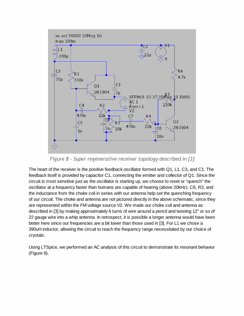
Figure 8 - Super regenerative receiver topology described in [3]
The heart of the receiver is the positive feedback oscillator formed with Q1, L1, C3, and C1. The feedback itself is provided by capacitor C1, connecting the emitter and collector of Q1. Since the circuit is most sensitive just as the oscillator is starting up, we choose to reset or “quench” the oscillator at a frequency faster than humans are capable of hearing (above 20kHz). C6, R3, and the inductance from the choke coil in series with our antenna help set the quenching frequency of our circuit. The choke and antenna are not pictured directly in the above schematic, since they are represented within the FM voltage source V2. We made our choke coil and antenna as described in [3] by making approximately 6 turns of wire around a pencil and twisting 12” or so of 22 gauge wire into a whip antenna. In retrospect, it is possible a longer antenna would have been better here since our frequencies are a bit lower than those used in [3]. For L1 we chose a 390uH inductor, allowing the circuit to reach the frequency range necessitated by our choice of crystals. Using LTSpice, we performed an AC analysis of this circuit to demonstrate its resonant behavior (Figure 9).
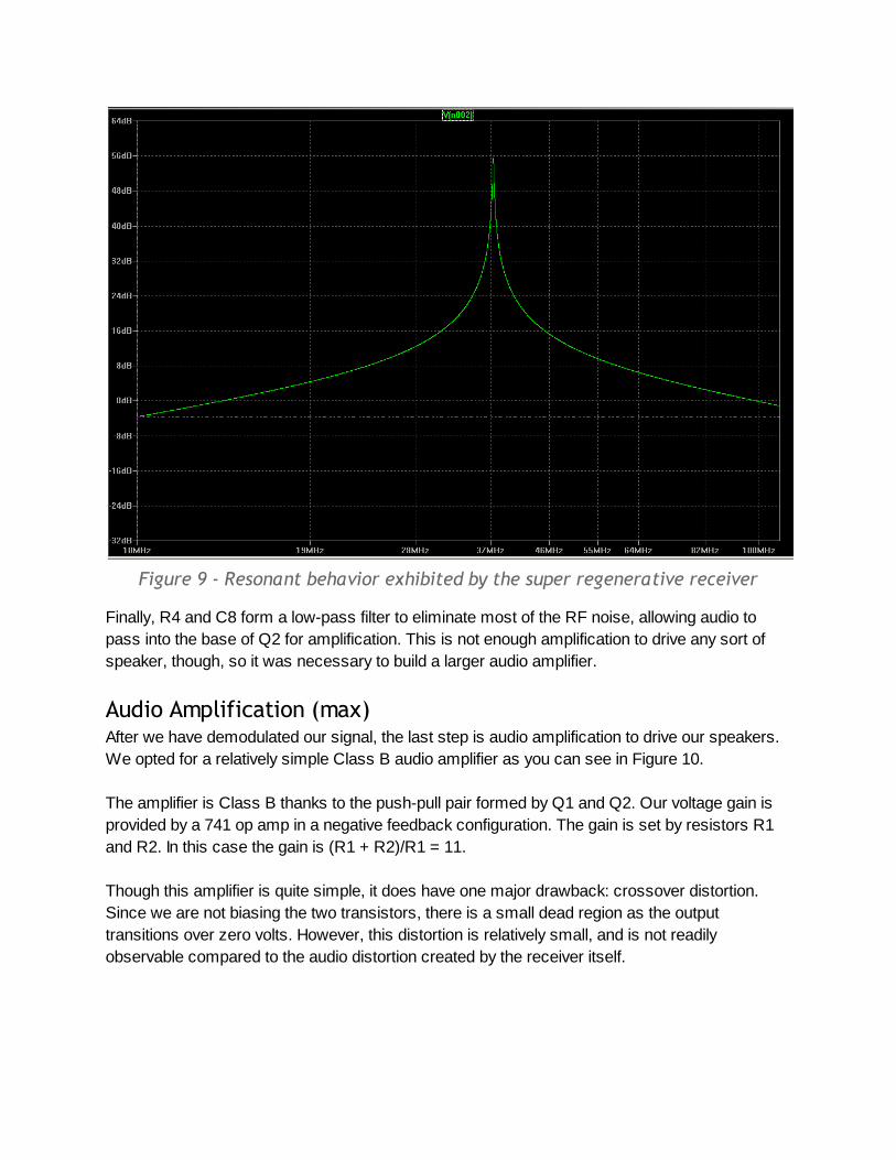
Figure 9 - Resonant behavior exhibited by the super regenerative receiver
Finally, R4 and C8 form a low-pass filter to eliminate most of the RF noise, allowing audio to pass into the base of Q2 for amplification. This is not enough amplification to drive any sort of speaker, though, so it was necessary to build a larger audio amplifier.
Audio Amplification (max) After we have demodulated our signal, the last step is audio amplification to drive our speakers. We opted for a relatively simple Class B audio amplifier as you can see in Figure 10. The amplifier is Class B thanks to the push-pull pair formed by Q1 and Q2. Our voltage gain is provided by a 741 op amp in a negative feedback configuration. The gain is set by resistors R1 and R2. In this case the gain is (R1 + R2)/R1 = 11. Though this amplifier is quite simple, it does have one major drawback: crossover distortion. Since we are not biasing the two transistors, there is a small dead region as the output transitions over zero volts. However, this distortion is relatively small, and is not readily observable compared to the audio distortion created by the receiver itself.
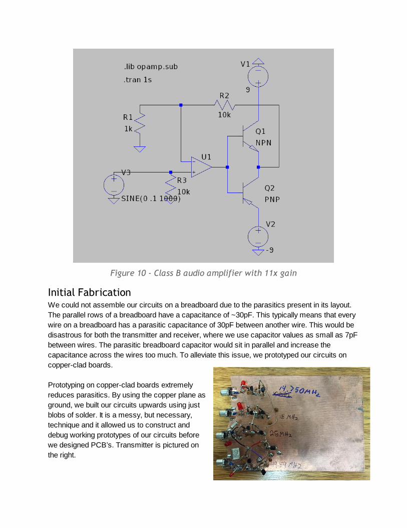
Figure 10 - Class B audio amplifier with 11x gain
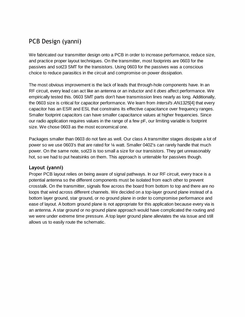
Initial Fabrication We could not assemble our circuits on a breadboard due to the parasitics present in its layout. The parallel rows of a breadboard have a capacitance of ~30pF. This typically means that every wire on a breadboard has a parasitic capacitance of 30pF between another wire. This would be disastrous for both the transmitter and receiver, where we use capacitor values as small as 7pF between wires. The parasitic breadboard capacitor would sit in parallel and increase the capacitance across the wires too much. To alleviate this issue, we prototyped our circuits on copper-clad boards. Prototyping on copper-clad boards extremely reduces parasitics. By using the copper plane as ground, we built our circuits upwards using just blobs of solder. It is a messy, but necessary, technique and it allowed us to construct and debug working prototypes of our circuits before we designed PCB’s. Transmitter is pictured on the right.
PCB Design (yanni) We fabricated our transmitter design onto a PCB in order to increase performance, reduce size, and practice proper layout techniques. On the transmitter, most footprints are 0603 for the passives and sot23 SMT for the transistors. Using 0603 for the passives was a conscious choice to reduce parasitics in the circuit and compromise on power dissipation. The most obvious improvement is the lack of leads that through-hole components have. In an RF circuit, every lead can act like an antenna or an inductor and it does affect performance. We empirically tested this. 0603 SMT parts don’t have transmission lines nearly as long. Additionally, the 0603 size is critical for capacitor performance. We learn from Intersil’s AN1325[4] that every capacitor has an ESR and ESL that constrains its effective capacitance over frequency ranges. Smaller footprint capacitors can have smaller capacitance values at higher frequencies. Since our radio application requires values in the range of a few pF, our limiting variable is footprint size. We chose 0603 as the most economical one. Packages smaller than 0603 do not fare as well. Our class A transmitter stages dissipate a lot of power so we use 0603’s that are rated for ⅛ watt. Smaller 0402’s can rarely handle that much power. On the same note, sot23 is too small a size for our transistors. They get unreasonably hot, so we had to put heatsinks on them. This approach is untenable for passives though.
Layout (yanni) Proper PCB layout relies on being aware of signal pathways. In our RF circuit, every trace is a potential antenna so the different components must be isolated from each other to prevent crosstalk. On the transmitter, signals flow across the board from bottom to top and there are no loops that wind across different channels. We decided on a top-layer ground plane instead of a bottom layer ground, star ground, or no ground plane in order to compromise performance and ease of layout. A bottom ground plane is not appropriate for this application because every via is an antenna. A star ground or no ground plane approach would have complicated the routing and we were under extreme time pressure. A top layer ground plane alleviates the via issue and still allows us to easily route the schematic.
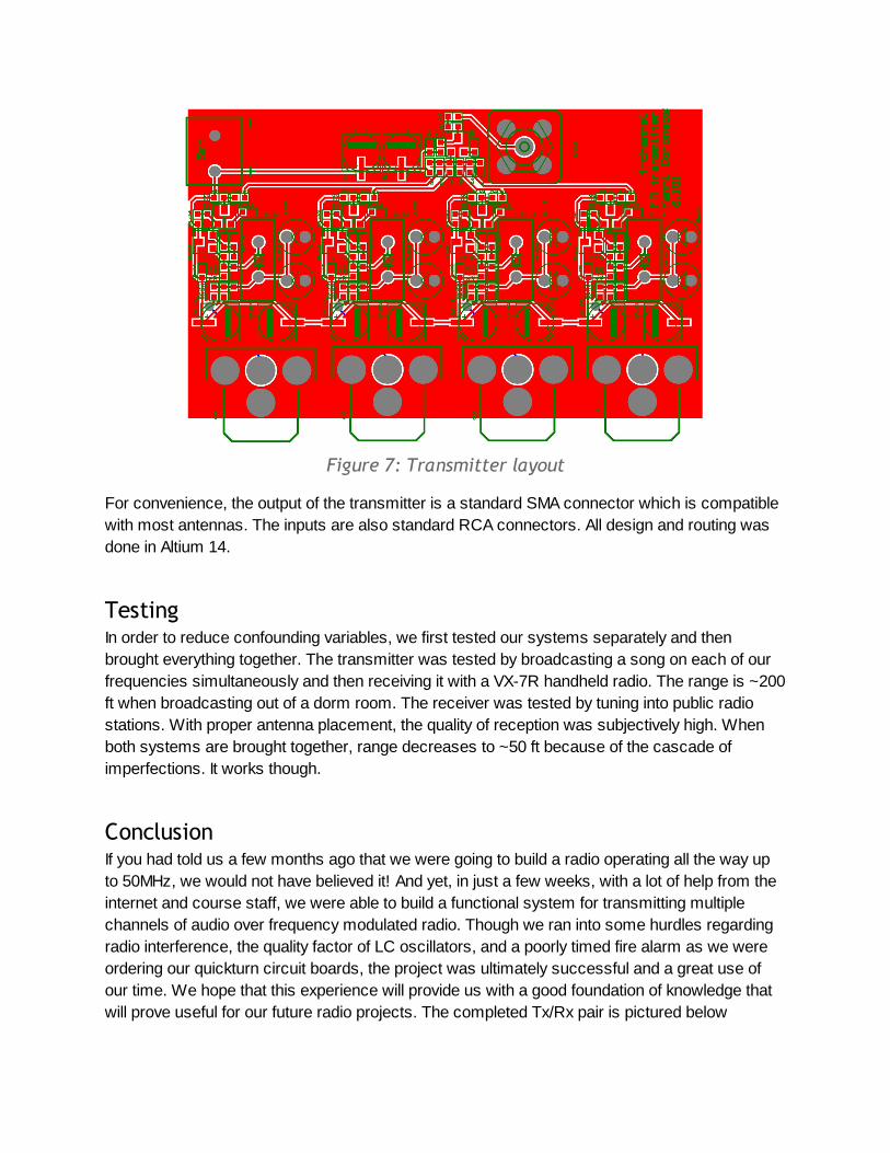
Figure 7: Transmitter layout
For convenience, the output of the transmitter is a standard SMA connector which is compatible with most antennas. The inputs are also standard RCA connectors. All design and routing was done in Altium 14.
Testing In order to reduce confounding variables, we first tested our systems separately and then brought everything together. The transmitter was tested by broadcasting a song on each of our frequencies simultaneously and then receiving it with a VX-7R handheld radio. The range is ~200 ft when broadcasting out of a dorm room. The receiver was tested by tuning into public radio stations. With proper antenna placement, the quality of reception was subjectively high. When both systems are brought together, range decreases to ~50 ft because of the cascade of imperfections. It works though.
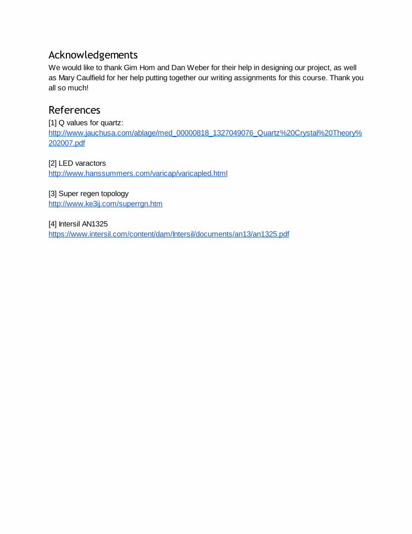
Conclusion If you had told us a few months ago that we were going to build a radio operating all the way up to 50MHz, we would not have believed it! And yet, in just a few weeks, with a lot of help from the internet and course staff, we were able to build a functional system for transmitting multiple channels of audio over frequency modulated radio. Though we ran into some hurdles regarding radio interference, the quality factor of LC oscillators, and a poorly timed fire alarm as we were ordering our quickturn circuit boards, the project was ultimately successful and a great use of our time. We hope that this experience will provide us with a good foundation of knowledge that will prove useful for our future radio projects. The completed Tx/Rx pair is pictured below
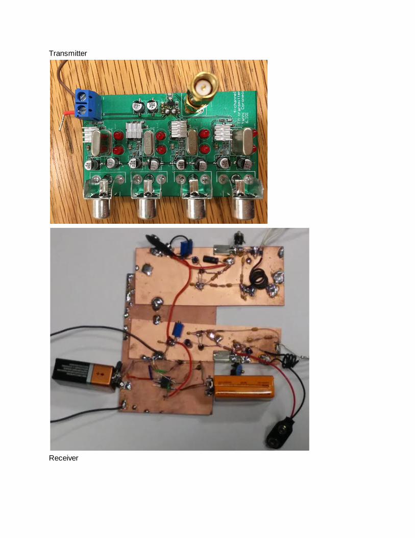
Transmitter
Receiver
Acknowledgements We would like to thank Gim Hom and Dan Weber for their help in designing our project, as well as Mary Caulfield for her help putting together our writing assignments for this course. Thank you all so much!
References [1] Q values for quartz: http://www.jauchusa.com/ablage/med_00000818_1327049076_Quartz%20Crystal%20Theory%202007.pdf [2] LED varactors http://www.hanssummers.com/varicap/varicapled.html [3] Super regen topology http://www.ke3ij.com/superrgn.htm [4] Intersil AN1325 https://www.intersil.com/content/dam/Intersil/documents/an13/an1325.pdf
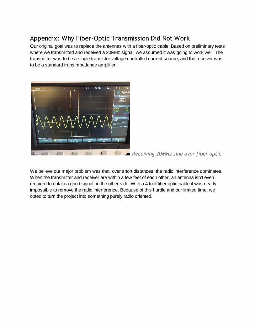
Appendix: Why Fiber-Optic Transmission Did Not Work Our original goal was to replace the antennas with a fiber-optic cable. Based on preliminary tests where we transmitted and received a 20MHz signal, we assumed it was going to work well. The transmitter was to be a single transistor voltage controlled current source, and the receiver was to be a standard transimpedance amplifier.
Receiving 20MHz sine over fiber optic
We believe our major problem was that, over short distances, the radio interference dominates. When the transmitter and receiver are within a few feet of each other, an antenna isn’t even required to obtain a good signal on the other side. With a 4 foot fiber optic cable it was nearly impossible to remove the radio interference. Because of this hurdle and our limited time, we opted to turn the project into something purely radio oriented.