Transformation Optics Using Graphene: One-Atom-Thick ...
166
University of Pennsylvania University of Pennsylvania ScholarlyCommons ScholarlyCommons Publicly Accessible Penn Dissertations 2012 Transformation Optics Using Graphene: One-Atom-Thick Optical Transformation Optics Using Graphene: One-Atom-Thick Optical Devices Based on Graphene Devices Based on Graphene Ashkan Vakil University of Pennsylvania, [email protected] Follow this and additional works at: https://repository.upenn.edu/edissertations Part of the Electrical and Electronics Commons, Electromagnetics and Photonics Commons, and the Physics Commons Recommended Citation Recommended Citation Vakil, Ashkan, "Transformation Optics Using Graphene: One-Atom-Thick Optical Devices Based on Graphene" (2012). Publicly Accessible Penn Dissertations. 715. https://repository.upenn.edu/edissertations/715 This paper is posted at ScholarlyCommons. https://repository.upenn.edu/edissertations/715 For more information, please contact [email protected].
Transcript of Transformation Optics Using Graphene: One-Atom-Thick ...

University of Pennsylvania University of Pennsylvania
ScholarlyCommons ScholarlyCommons
Publicly Accessible Penn Dissertations
2012
Transformation Optics Using Graphene: One-Atom-Thick Optical Transformation Optics Using Graphene: One-Atom-Thick Optical
Devices Based on Graphene Devices Based on Graphene
Ashkan Vakil University of Pennsylvania, [email protected]
Follow this and additional works at: https://repository.upenn.edu/edissertations
Part of the Electrical and Electronics Commons, Electromagnetics and Photonics Commons, and the
Physics Commons
Recommended Citation Recommended Citation Vakil, Ashkan, "Transformation Optics Using Graphene: One-Atom-Thick Optical Devices Based on Graphene" (2012). Publicly Accessible Penn Dissertations. 715. https://repository.upenn.edu/edissertations/715
This paper is posted at ScholarlyCommons. https://repository.upenn.edu/edissertations/715 For more information, please contact [email protected].

Transformation Optics Using Graphene: One-Atom-Thick Optical Devices Based Transformation Optics Using Graphene: One-Atom-Thick Optical Devices Based on Graphene on Graphene
Abstract Abstract Metamaterials and transformation optics have received considerable attention in the recent years, as they have found an immense role in many areas of optical science and engineering by offering schemes to control electromagnetic fields. Another area of science that has
been under the spotlight for the last few years relates to exploration of graphene, which is formed of carbon atoms densely packed into a honey-comb lattice. This material exhibits unconventional electronic and optical properties, intriguing many research groups across
the world including us. But our interest is mostly in studying interaction of electromagnetic waves with graphene and applications that might follow.
Our group as well as few others pioneered investigating prospect of graphene for plasmonic devices and in particular plasmonic metamaterial structures and transformation optical devices. In this thesis, relying on theoretical models and numerical simulations, we
show that by designing and manipulating spatially inhomogeneous, nonuniform conductivity patterns across a flake of graphene, one can have this material as a one-atom-thick platform for infrared metamaterials and transformation optical devices. Varying the graphene chemical potential by using static electric field allows for tuning the graphene conductivity in the terahertz and infrared frequencies. Such design flexibility can be exploited to create "patches" with differing conductivities within a single flake of graphene. Numerous photonic functions and metamaterial concepts are expected to follow from such platform. This work presents several numerical examples demonstrating these functions.
Our findings show that it is possible to design one-atom-thick variant of several optical elements analogous to those in classic optics. Here we theoretically study one-atom-thick metamaterials, one-atom-thick waveguide elements, cavities, mirrors, lenses, Fourier optics and finally a few case studies illustrating transformation optics on a single sheet of graphene in mid-infrared wavelengths.
Degree Type Degree Type Dissertation
Degree Name Degree Name Doctor of Philosophy (PhD)
Graduate Group Graduate Group Electrical & Systems Engineering
First Advisor First Advisor Nader Engheta
Keywords Keywords Graphene, Metamaterials, Photonics, Plasmonics, Transformation Optics
Subject Categories Subject Categories Electrical and Electronics | Electromagnetics and Photonics | Physics
This dissertation is available at ScholarlyCommons: https://repository.upenn.edu/edissertations/715

TRANSFORMATION OPTICS USING GRAPHENE:
ONE-ATOM-THICK OPTICAL DEVICES BASED ON GRAPHENE
Ashkan Vakil
A DISSERTATION
in
Electrical and Systems Engineering
Presented to the Faculties of the University of Pennsylvania
in
Partial Fulfillment of the Requirements for
the Degree of Doctor of Philosophy
2012
Supervisor of DissertationNader Engheta
H. Nedwill Ramsey Professor of Electrical and Systems Engineering
Graduate Group ChairpersonSaswati Sarkar
Professor of Electrical and Systems Engineering
Dissertation Committee:
Dwight L. Jaggard, Professor of Electrical and Systems Engineering
Cherie R. Kagan, Professor of Electrical and Systems Engineering
Alan T. Charlie Johnson, Jr., Professor of Physics and Astronomy

To my family and Samira,
for their unconditional love and support.
ii
Acknowledgments
This thesis could not have been written without the support of my advisor and mentor,
Professor Nader Engheta; I am truly indebted to him for his meticulous comments and
his encouragements while I was writing this thesis. Professor Engheta taught me how to
think independently and most importantly how to think “outside the box”. Not only a great
mentor, he has been a true friend throughout these years. Hiskindness will forever be of
immense value to me.
I want to express my sincere gratitude to my committee members, Professors Dwight
Jaggard, A. T. Charlie Johnson, and Cherie Kagan for their critical comments on my work
and for their suggestions to improve quality of my research.
I am grateful to my friends and colleagues at Penn, who helpedme in scientific as-
pects or otherwise during these years. Special thanks to Brian Edwards, Uday Chettiar and
Marjan Saboktakin.
In addition, I would like to thank Professors Andrea Alu andMario Silveirinha, who
helped me a great deal with scientific research, and also my previous colleagues, Dr.
Alessia Polemi and Dr. Olli Luukkonen for making the work environment fun and pro-
ductive.
A special to thanks my friends, Pouya, Arash, Sina, Rouzbeh,Matteo and Chiara. With-
iii

out them, my years in Philadelphia would not have been as pleasant.
And of course, my most deepest thanks to my parents, Farnaz and Farzin, for their
everlasting love, and to my brother, Sam, who provided me with his unconditional support.
I would not have made it this far without them...
Last but not least, I truly and deeply thank my girlfriend, Samira, for her love and
endless patience, and for being by my side, even when I was irritable and frustrated...
iv

ABSTRACT
TRANSFORMATION OPTICS USING GRAPHENE:
ONE-ATOM-THICK OPTICAL DEVICES BASED ON GRAPHENE
Ashkan Vakil
Nader Engheta
Metamaterials and transformation optics have received considerable attention in the recent
years, as they have found an immense role in many areas of optical science and engineering
by offering schemes to control electromagnetic fields. Another area of science that has
been under the spotlight for the last few years relates to exploration of graphene, which is
formed of carbon atoms densely packed into a honey-comb lattice. This material exhibits
unconventional electronic and optical properties, intriguing many research groups across
the world including us. But our interest is mostly in studying interaction of electromagnetic
waves with graphene and applications that might follow.
Our group as well as few others pioneered investigating prospect of graphene for plas-
monic devices and in particular plasmonic metamaterial structures and transformation op-
tical devices. In this thesis, relying on theoretical models and numerical simulations, we
show that by designing and manipulating spatially inhomogeneous, nonuniform conductiv-
ity patterns across a flake of graphene, one can have this material as a one-atom-thick plat-
form for infrared metamaterials and transformation optical devices. Varying the graphene
chemical potential by using static electric field allows fortuning the graphene conductivity
in the terahertz and infrared frequencies. Such design flexibility can be exploited to create
v

“patches” with differing conductivities within a single flake of graphene. Numerous pho-
tonic functions and metamaterial concepts are expected to follow from such platform. This
work presents several numerical examples demonstrating these functions.
Our findings show that it is possible to design one-atom-thick variant of several optical
elements analogous to those in classic optics. Here we theoretically study one-atom-thick
metamaterials, one-atom-thick waveguide elements, cavities, mirrors, lenses, Fourier op-
tics and finally a few case studies illustrating transformation optics on a single sheet of
graphene in mid-infrared wavelengths.
vi

Contents
Contents vii
List of Figures x
1 Introduction 1
1.1 Metamaterials and transformation optics . . . . . . . . . . . .. . . . . . . 1
1.1.1 Metamaterials . . . . . . . . . . . . . . . . . . . . . . . . . . . . . 1
1.1.2 Metamaterials and transformation optics . . . . . . . . . .. . . . . 5
1.2 Integration of electronics and photonics: plasmonics as a bridge . . . . . . 7
1.3 Literature Review . . . . . . . . . . . . . . . . . . . . . . . . . . . . . . . 11
2 Theoretical Background 15
2.1 Complex conductivity model for graphene . . . . . . . . . . . . .. . . . . 15
2.1.1 Analytic expression for complex conductivity . . . . . .. . . . . . 15
2.1.2 Numerical results for optical conductivity . . . . . . . .. . . . . . 18
2.2 Surface Plasmon-Polariton Surface Waves on Graphene . .. . . . . . . . . 24
2.2.1 A comparison between graphene and silver . . . . . . . . . . .. . 31
2.2.2 Foundations for design of metamaterials . . . . . . . . . . .. . . . 37
vii

2.2.3 Dydic Green’s functions for graphene . . . . . . . . . . . . . .. . 39
2.2.4 Fresnel reflection for SPP surface waves . . . . . . . . . . . .. . . 47
2.2.5 Scattering from subwavelength graphene patches . . . .. . . . . . 57
2.2.6 Coupling between an emitter and graphene SPPs . . . . . . .. . . 62
2.2.7 Excitation of SPPs . . . . . . . . . . . . . . . . . . . . . . . . . . 64
3 Graphene Metamaterials & Transformation Optics 70
3.1 One-atom-thick waveguide elements . . . . . . . . . . . . . . . . .. . . . 73
3.1.1 One-atom-thick waveguide . . . . . . . . . . . . . . . . . . . . . . 73
3.1.2 One-atom-thick waveguide using edge modes . . . . . . . . .. . . 77
3.1.3 One-atom-thick splitter/combiner . . . . . . . . . . . . . . . . . . 78
3.1.4 One-atom-thick optical fiber . . . . . . . . . . . . . . . . . . . . .79
3.2 One-atom-thick cavities . . . . . . . . . . . . . . . . . . . . . . . . . .. . 82
3.2.1 Design of one-atom-thick cavities . . . . . . . . . . . . . . . .. . 84
3.2.2 Analysis of one-atom-thick cavities . . . . . . . . . . . . . .. . . 90
3.3 One-atom-thick reflectors . . . . . . . . . . . . . . . . . . . . . . . . .. . 95
3.3.1 One-atom-thick straight line mirror . . . . . . . . . . . . . .. . . . 95
3.4 Transformation optics using graphene . . . . . . . . . . . . . . .. . . . . 99
3.4.1 Luneburg lens with graphene . . . . . . . . . . . . . . . . . . . . . 100
4 Fourier Optics on Graphene 108
4.1 Lensing mechanism on graphene . . . . . . . . . . . . . . . . . . . . . .. 109
4.2 One-atom-thick 4f system . . . . . . . . . . . . . . . . . . . . . . . . . .. 114
5 Conclusion 118
5.1 Summary . . . . . . . . . . . . . . . . . . . . . . . . . . . . . . . . . . . 118
viii

5.2 Future directions . . . . . . . . . . . . . . . . . . . . . . . . . . . . . . . 121
5.3 Final Thoughts . . . . . . . . . . . . . . . . . . . . . . . . . . . . . . . . 122
A Circuit Analogy for Conductivity 125
B Methods for Numerical Simulations 127
C Dispersion of Graphene Nanoribbons 129
D Graphene Nano-circtuits 131
E Matlab Code 136
Bibliography 139
ix

List of Figures
1.1 3D optical metamaterial . . . . . . . . . . . . . . . . . . . . . . . . . . .. . . 4
1.2 Concept of graphene metamaterial . . . . . . . . . . . . . . . . . . .. . . . . 9
1.3 Research in graphene . . . . . . . . . . . . . . . . . . . . . . . . . . . . . .. 11
2.1 Real and imaginary part of the conductivity . . . . . . . . . . .. . . . . . . . 20
2.2 Complex conductivity as a function of frequency . . . . . . .. . . . . . . . . 21
2.3 Contribution of inter- & intra-band transitions to conductivity . . . . . . . . . . 23
2.4 A free-standing graphene layer lying inx-y plane . . . . . . . . . . . . . . . . 25
2.5 Free-standing slab of material . . . . . . . . . . . . . . . . . . . . .. . . . . . 28
2.6 TM surface plasmon-polaritons along a graphene layer . .. . . . . . . . . . . 30
2.7 Surface plasmon-polaritons along metal-dielectric interface . . . . . . . . . . . 32
2.8 Characteristics of TM SPP surface waves along graphene .. . . . . . . . . . . 34
2.9 Nonuniform conductivity using uneven ground plane . . . .. . . . . . . . . . 35
2.10 Second idea to create inhomogeneous conductivity patterns . . . . . . . . . . . 36
2.11 Fresnel reflection for an SPP surface wave . . . . . . . . . . . .. . . . . . . . 37
2.12 Horizontal electric dipole . . . . . . . . . . . . . . . . . . . . . . .. . . . . . 40
2.13 Distribution ofEy for a horizontal electric dipole . . . . . . . . . . . . . . . . 45
x

2.14 Distribution ofEx andEz for a horizontal electric dipole . . . . . . . . . . . . . 46
2.15 In-plane Fresnel reflection of SPP surface waves . . . . . .. . . . . . . . . . . 47
2.16 Distribution ofEy for a guided edge wave . . . . . . . . . . . . . . . . . . . . 49
2.17 Reflection from edges: Transmission line analogy . . . . .. . . . . . . . . . . 51
2.18 Reflection from edges (scenario 1) . . . . . . . . . . . . . . . . . .. . . . . . 53
2.19 Reflection from edges (scenario 2) . . . . . . . . . . . . . . . . . .. . . . . . 54
2.20 Reflection from edges (scenario 3) . . . . . . . . . . . . . . . . . .. . . . . . 57
2.21 Scattering of SPPs by a nanondisk . . . . . . . . . . . . . . . . . . .. . . . . 59
2.22 Polarizability of graphene nanondisk . . . . . . . . . . . . . .. . . . . . . . . 61
2.23 Excitation of SPPs using diffraction grating . . . . . . . . . . . . . . . . . . . 65
2.24 Excitation of SPPs using array of subwavelength disks .. . . . . . . . . . . . 67
2.25 Dipole radiation coupled to graphene SPPs . . . . . . . . . . .. . . . . . . . . 68
3.1 Flatland metamaterial . . . . . . . . . . . . . . . . . . . . . . . . . . . .. . . 71
3.2 Electric field distribution in a flatland metamaterial . .. . . . . . . . . . . . . 72
3.3 Graphene nanoribbon as waveguide . . . . . . . . . . . . . . . . . . .. . . . 74
3.4 Symmetric and anti-symmetric modes of graphene nanoribbons . . . . . . . . . 75
3.5 Dispersion relation for a graphene nanoribbon waveguide . . . . . . . . . . . . 76
3.6 Bent ribbon waveguide . . . . . . . . . . . . . . . . . . . . . . . . . . . . .. 79
3.7 Graphene splitter . . . . . . . . . . . . . . . . . . . . . . . . . . . . . . . .. 80
3.8 One-atom-thick variant of optical fiber . . . . . . . . . . . . . .. . . . . . . . 81
3.9 1D one-atom-thick resonant cavity . . . . . . . . . . . . . . . . . .. . . . . . 84
3.10 Characteristics of 1D graphene cavity . . . . . . . . . . . . . .. . . . . . . . 86
3.11 Electric field distribution for 1D graphene cavity . . . .. . . . . . . . . . . . . 87
3.12 2D one-atom-thick resonant cavity . . . . . . . . . . . . . . . . .. . . . . . . 88
xi

3.13 Characteristics of 2D graphene cavity . . . . . . . . . . . . . .. . . . . . . . 90
3.14 Electric field distribution for 2D graphene cavity . . . .. . . . . . . . . . . . . 91
3.15 Straight-line mirror using graphene . . . . . . . . . . . . . . .. . . . . . . . . 98
3.16 One-atom-thick parabolic mirror . . . . . . . . . . . . . . . . . .. . . . . . . 99
3.17 Luneburg lens: going from 3D to 2D . . . . . . . . . . . . . . . . . . .. . . . 101
3.18 Simulation results for Luneburg lens . . . . . . . . . . . . . . .. . . . . . . . 104
3.19 Schematic of a superlens . . . . . . . . . . . . . . . . . . . . . . . . . .. . . 104
3.20 Flatland “superlens” . . . . . . . . . . . . . . . . . . . . . . . . . . . .. . . . 106
4.1 Lensing on graphene . . . . . . . . . . . . . . . . . . . . . . . . . . . . . . .110
4.2 Graphene lensing: point source illumination . . . . . . . . .. . . . . . . . . . 113
4.3 Graphene lensing: “line” wave illumination . . . . . . . . . .. . . . . . . . . 115
4.4 4f System on graphene . . . . . . . . . . . . . . . . . . . . . . . . . . . . . .116
5.1 Tomography using graphene . . . . . . . . . . . . . . . . . . . . . . . . .. . 123
A.1 Parallel RLC circuit. . . . . . . . . . . . . . . . . . . . . . . . . . . . . .. . 126
D.1 Optical nanocircuits using graphene . . . . . . . . . . . . . . . .. . . . . . . 132
D.2 Series graphene circuit . . . . . . . . . . . . . . . . . . . . . . . . . . .. . . 133
D.3 Series graphene circuit impedance . . . . . . . . . . . . . . . . . .. . . . . . 135
xii

1
Chapter 1
Introduction
1.1 Metamaterials and transformation optics
1.1.1 Metamaterials
To build an electromagnetic (EM) device with certain functionalities, we need to be able
to transmit, receive, confine, guide and manipulate EM waves. Over years, scientists and
engineers have come up with myriad of brilliant designs and schemes to build devices per-
forming these functions. For example antennas have been designed to transmit and receive
waves, waveguides to confine and guide them, and polarizers and filters to manipulate
them [7, 86]. All these are based on a central notion: exploiting “materials” to control,
manipulate and direct fields and waves [12, 26, 83].
Although we are blessed with a wide range of materials in nature, the variety of devices
that can be built from these materials is inevitably limitedby spectrum of properties they
exhibit. And indeed many desired electromagnetic properties, such as monopole magnets
or negative refraction, seem to be missing in nature [12, 26]—or at least we have been

CHAPTER 1. INTRODUCTION 2
out of luck to find the materials exhibiting those desired properties. But why might these
missing properties be important? An example may shed light on the significance of such
properties. Let us take a look at the case of negative refraction.
Victor Veselago, in a paper published in 1967∗, predicted if materials with simulta-
neously negative values ofǫ andµ – negative refractive index (NRI) or double-negative
(DNG) materials – were ever found, they would exhibit unconventional properties unlike
that of any known materials. For example for a plane wave in a DNG material the direction
of the Poynting vector would be antiparallel to the direction of the phase velocity. The
impact of such property can be tremendous; several interesting proposals can follow from
such property. For instance consider perfect lensing [81] and subwavelength resonant cav-
ities using DNG materials [22]. These examples indicate thewide scope of possibilities
that can emerge from the missing properties in nature.
However no theory can be of much interest if the technology torealizing it is not avail-
able, and maybe that was why Veselago had to wait for a few decades to be praised for
his work; his paper did not receive much attention at the timesimply because no available
material had negativeǫ andµ at the same time. But is there any physical law that precludes
this possibility?
One region of frequency where permittivity and permeability attain negative values is
around their resonance† as driving electric or magnetic field becomes out of phase with
the huge polarization induced in the material—that is the electric and magnetic dipole
moment cannot respond fast enough as the polarization of incident field flips. However
materials with simultaneously negativeǫ andµ are not observed in nature simply because
interestingly the fundamental electric and magnetic processes behind resonant phenomena,
in materials we have identified so far, do not occur at the samefrequencies [84]. The
∗The English translation of the original paper was publishedin 1968 [111].†In addition Drude permittivity of an electron gas can take negative values below plasma frequency.

CHAPTER 1. INTRODUCTION 3
Mother Nature leaves it for us to design structures that exhibit negative refractive index‡.
The idea of artificially structuring composites or materials to exhibit certain proper-
ties is not new; the first attempts to build such composites can be traced back to the late
nineteen century and first half of twentieth century [24, 26]. For example in late 1890’s, Ja-
gadish Chandra Bose explored twisted structure that could rotate the plane of polarization,
resembling what today called chiral structures [24]. Or in 1914, Karl Ferdinand Lindman
studied chiral media constructed from collection of wire helices [24]. Later in the 1940’s,
1950’s and 1960’s, there were attempts to design and fabricate “artificial dielectric” for ap-
plications in lightweight lenses for microwave frequencies [24]. In the 1980’s and 1990’s,
once again artificial complex materials and in particular chiral structures became subject
of interest for building microwave components [21, 24].
However, due to the technological constraints, miniaturizing these structures has always
been a challenge in this territory. Fortunately advances innanotechnology and material sci-
ences over the last couple of decades have removed some of thebarriers and largely boosted
our ability to fabricate different forms of materials and structures. Nowadays chemistsand
material engineers are able to tailor materials at atomic level. This capability allows for
engineering materials with desired electromagnetic properties that might be missing or dif-
ficult to find in nature. And of course following such flexibility resides a continuum of
novel ideas for electromagnetic and optical design. As a result, last few years we have
witnessed resurrection of the field of “metamaterial” (in today’s terminology).
Field of “metamaterial” has brought scientists and engineers from electromagnetics and
material sciences to realize new classes of electromagnetic materials that are constructed
by embedding subwavelength inclusions or inhomogeneitiesin a host medium rather than
by controlling chemical composition. The geometrical characteristics (i.e., size and shape),
‡The first realization of an NRI material was in 2001 by a group from the University of California, SanDiego [96].

CHAPTER 1. INTRODUCTION 4
Figure 1.1: An example of a 3D optical meta-material: uniaxial photonic metamaterial com-posed of three-dimensional gold helices ar-ranged on a two-dimensional square lattice.This structure can act as a broadband circu-lar polarizer [32]. The structure was real-ized by 3D direct laser-writing of helices inpositive-tone photoresist. The polymer wasremoved by plasma etching, resulting in asquare array of freestanding gold helices. FormRef. 32 [J. K. Gansel et. al, “Gold helix pho-tonic metamaterial as broadband circular polar-izer”, Science325, 5947 (2009)]. Reprintedwith permission from the AAAS. [http://www.sciencemag.org/content/325/5947/1513].
periodicity, optical properties of these inclusions and inhomogeneities, and electromagnetic
characteristics of host media determine the electromagnetic response of the composite ma-
terials or structures. Having control over these features the electromagnetic response of
materials can be tuned at will to show a certain behavior desired by the electromagnetic
design engineers. In essence, electromagnetic response ofmaterials can be described by
their effective permittivity and permeability, and depending on thevalue and sign of these
two quantities, we can identify several classes of metamaterials: double-positive metama-
terials, double-negative metamaterials, single-negative metamaterials (ǫ < 0 andµ > 0)
or (ǫ > 0 andµ < 0), extreme-parameter metamaterials (for example epsilon-near-zero
or epsilon-very-large metamaterials). These are materials with properties that may not be
easily found in nature. Chirality and anisotropy are other material properties that can be
tailored artificially to produce materials with desired optical response. A discussion of
different metamaterial classes can be found in Refs. 12, 26 and 97. Figure 1.1 is an illus-
tration of a 3D optical metamaterial fabricated by Wegener group in 2009 [32], indicating
how nowadays scientists can fabricate sophisticated miniaturized metamaterial structures.
This structure can act as a broadband circular polarizer.

CHAPTER 1. INTRODUCTION 5
We would like to conclude our brief discussion with a formal definition for metamate-
rials. As it appears the term metamaterials in the literature has been widely used and there
is no universal definition for metamaterials. Cai & Shalaev [12] provide the following
definition:
“A metamaterial is an artificially structured material which attains its prop-
erties from the unit structure rather than the constituent materials. A
metamaterial has an inhomogeneity scale that is much smaller than the
wavelength of interest, and its electromagnetic response is expressed in
terms of homogenized material parameters.”
There are other equivalent definitions in the literature. Inprinciple all these definitions
refer to engineered structures that are constructed by embedding subwavelength inclusions
in a host medium. Next we discuss transformation optics and its connection to metamate-
rials.
1.1.2 Metamaterials and transformation optics
As we mentioned in section 1.1.1, electromagnetic design isall about controlling and ma-
nipulating the EM fields and waves by exploiting materials ina proper way to reflect and
refract and direct them to form desired patterns. Transformation optics offers a recipe to
tailor material properties at subwavelength scale to exhibit a desired function [83]. Now
the correspondence between transformation optics (TO) andmetamaterials becomes clear.
TO provides a design strategy and using metamaterials one can realize that design thanks
to today’s capacity in fabrication.
Transformation optics can be imagined as reverse-engineering of the optical device
we seek. First the field lines in an empty space are transformed into a desired configura-

CHAPTER 1. INTRODUCTION 6
tion associated with the desired optical device [83]. SinceMaxwell’s equations are form-
invariant, meaning that they maintain the same form in both coordinate systems [57, 83],
the optical parameters for Maxwell’s equations need to be scaled accordingly in the trans-
formed coordinate system (coordinate system associated with the optical device). Then
based on the transformation, the optical parameters (permittivity and permeability) for re-
alizing the optical device can be retrieved. A famous example of transformation optics is
the optical cloak [83], although this technique has other profound applications in optical
design. For example later in chapter 3, we show an example of transformation optics that
might find application in optical signal processing.
There have been a large interest and several developments intransformation optics since
its official introduction in 2006. A recent review is given in Ref. 82. In particular transfor-
mation optics has been successfully applied to plasmonic systems to control propagation
of special type of electromagnetic wave called surface plasmon-polariton (SPP) surface
waves [44].
In this work our goal is to show that “graphene”, which is a monolayer of carbon
atoms, can serve as a new platform forplasmonic metamaterialsandtransformation optical
devicesowing to its exotic features and the design freedom it offers. Before talking about
graphene, however, we would like to get a perspective of the field of plasmonics. What
is an SPP surface wave? And why might graphene be a better platform for plasmonic
metamaterials rather than noble metals such as silver and gold that, conventionally, have
long been the favorite choices in this territory?

CHAPTER 1. INTRODUCTION 7
1.2 Integration of electronics and photonics: plasmonicsas a bridge
The goal of electronic engineers has always been design of miniaturized devices that are
light, cheap, low power and of course equally important fastin processing and transmitting
information. Since revolutionary invention of integratedcircuits (ICs) by Jack Kilby in
1959, electronics has certainly come a long way: from 7/16-by-1/16-inches IC that Kilby
built to today’s nanoscale electronics [51]. As Moore predicted [70], the number of tran-
sistors in integrated circuits has continuously and rapidly grown since the invention of ICs,
suggesting that we have been able to process data faster without considerably increasing
the size of the electronic circuits. This indicates how flourishing this field has been over
the past few decades. But it seems that over the last couple ofyears (since 2005 [102])
we have not seen stunning improvements in microprocessors.This raises the question that
whether we are approaching a plateau in rate of processing per volume. If so, what is the
reason?
The answer can be traced back to constant-field scaling rule,which tells us that the
voltage for operation of transistors must decrease in line with downscaled dimensions of
transistors. But downscaling dimensions might be possibleto a certain level, after which
the minimum gate voltage-swing necessary to switch the device from “off” state to “on”
state could be just too small. From design perspective this means either excessive leakage
current (dissipation) in the “off” state or low current – slow circuits – in the “on” state [102].
Neither is favorable. So how can we overcome this obstacle?
Integration of electronics and photonics is one promising solution to go around this
hurdle [78]. Photonic devices are generally faster simply because they carry higher fre-
quency optical signals, enabling faster signal processingcompared with electronic devices.
For years Silicon has been the favorite choice for optoelectronics devices, bringing elec-

CHAPTER 1. INTRODUCTION 8
tronics and photonics under one umbrella. Probably one of the most important reasons for
this popularity is the promise of Silicon for integration ofelectronics and photonics. But
yet, further downsizing Silicon-photonics devices may notbe a straightforward task, since
some of these devices such as optical waveguides are necessarily bulky to carry volumetric
waves. This hampers the progress toward integration of these two technologies and limits
the extent of downscaling. Emerging field of nanoplasmonics, which is a major part of the
field of photonics, can resolve this issue by providing a collection of techniques to confine
light waves at scales much smaller than the wavelength. Nanoplasmonics then allows for
design of elements (e.g., waveguide) that are much smaller than their photonic counterparts
and facilitate integration of two technologies. Field of plasmonics deals with engineering
of surface plasmons, exactly as electronics and photonics is science of manipulation of
electrons and photons, respectively. So what are surface plasmons?
Surface plasmons are collective oscillation of electrons at an interface between two
media whose values of the real part of permittivity have different signs [63]. If the light
incident on such an interface can couple with these surface-plasmons, the result is a highly
confined propagating electromagnetic wave known as surfaceplasmon polariton (SPP) sur-
face wave. Thanks to advances in nanofabrication, nowadaysultra-small plasmonics sys-
tems, even as small as few hundreds of nanometers, are feasible [10]. The concept of
metamaterials can also be applied to plasmonics structures; one can tailor electromagnetic
properties of a plasmonic material or structure to obtain a certain response from the system.
Owing to their ability to support the surface-plasmon polariton surface waves, in the
infrared and visible regimes, the noble metals, such as silver and gold, have been popular
materials in constructing plasmonic systems and many metamaterial structures [12]. As
our discussion to this point might hint, the key concept in design of metamaterials and
transformation optical devices is “tunability”. However,tuning permittivity functions of
noble metals is not an easy task. In addition the existence ofmaterial losses, especially

CHAPTER 1. INTRODUCTION 9
Vbias
!
!
!
!
!
!
!
!
!
!
!
!
!
!
!
!
!
!
!
!
"
Figure 1.2: Concept of graphene metamaterial:Can we have metamaterials and transformationoptics on graphene merely by varying its localconductivity?
at visible wavelengths, degrades the quality of the plasmonresonance and limits the rel-
ative propagation lengths of SPP waves along the interface between metals and dielectric
materials.
These deficiencies limit the functionality of some of available metamaterials and trans-
formation optical devices. In this work, we show that graphene can serve as a new platform
for metamaterials and transformation optical devices thatcan, under certain conditions, al-
leviate these issues. Overall there are three features thatmake graphene an excellent choice
for these purposes at least for mid-IR wavelengths
• Tunability: Most probably tunability of graphene is the most exciting feature of this
exotic material. We will see in chapter 2 that graphene conductivity can be controlled
using chemical doping or static electric bias. The basic idea is that whether we can
tailor behavior of a single layer of graphene by changing itsconductivity locally and
inhomogeneously (see Fig. 1.2). The ability to control and vary graphene optical
properties offers flexibility in design of electromagnetic systems based on graphene.
• Integration: After its first isolation in 2004 [76], graphene has been in spotlight for
its exotic electronic transport properties [74, 75] and suitability for optoelectronic
applications [5, 13, 69, 80, 88, 114]. As this work and several others show [41, 47,

CHAPTER 1. INTRODUCTION 10
54], graphene is also an excellent platform for plasmonics applications, suggesting
prospects for graphene as the bridge between electronics and plasmonics.
• Low material losses: As our studies show (see section 2.2.1) graphene has low mate-
rial losses, qualifying this one-atom-thick layer as a hostfor electromagnetic and op-
tical systems. It is worth mentioning that, in a recent article, Tassin et. al [101] claim
that graphene losses are considerable and thus the propagation length of the SPP
waves along graphene is at best just less than 3λSPP for IR frequencies. Their con-
clusion is based on experimental results presented in Ref. 58, in which the reported
real part of the conductivity, which accounts for losses, isrelatively large. However
graphene losses are dependent on the fabrication processes; cleaner graphene sam-
ples might result in lower losses and higher propagation lengths. To address this
objection, Tassin et. al use conductivity values reported in two theoretical papers that
predict large values for the real part of conductivity [36, 85]. It may not be fair to
draw such a general conclusion based on only two theoreticalpapers, whose their
results have not been confirmed by any experiments. Interestingly for the frequency
region of interest in this thesis, for typical values of chemical potential, the real part
of the conductivity reported by Ref. 58 (experimental paper) is much less than the
one reported in Ref. 36 (theory paper). This brings into question the general conclu-
sion of Tassin et. al in Ref. 101 that graphene is not a good host for surface plasmon
polaritons. The absolute resolution of this debate is remained unanswered until fur-
ther experiments are conducted in the future.
In addition, in recent years we have observed a rapid growth in graphene nanofabrication
capabilities that can facilitate realization of ultra-compact photonic and plasmonic devices
based on this material.
CHAPTER 1. INTRODUCTION 11
Before we start our formal discussion, it is laudable to givea brief review of literature
relevant to our proposal.
1.3 Literature Review
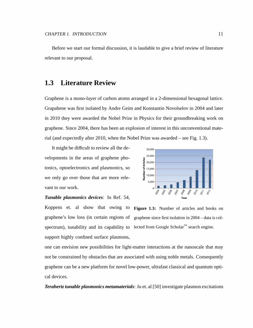
Graphene is a mono-layer of carbon atoms arranged in a 2-dimensional hexagonal lattice.
Grapahene was first isolated by Andre Geim and Konstantin Novolselov in 2004 and later
in 2010 they were awarded the Nobel Prize in Physics for theirgroundbreaking work on
graphene. Since 2004, there has been an explosion of interest in this unconventional mate-
rial (and expectedly after 2010, when the Nobel Prize was awarded – see Fig. 1.3).
0
5,000
10,000
15,000
20,000
25,000
30,000
Nu
mb
er
of
Art
icle
s
Year
Figure 1.3: Number of articles and books on
graphene since first isolation in 2004 – data is col-
lected from Google Scholar™ search engine.
It might be difficult to review all the de-
velopments in the areas of graphene pho-
tonics, optoelectronics and plasmonics, so
we only go over those that are more rele-
vant to our work.
Tunable plasmonics devices: In Ref. 54,
Koppens et. al show that owing to
graphene’s low loss (in certain regions of
spectrum), tunability and its capability to
support highly confined surface plasmons,
one can envision new possibilities for light-matter interactions at the nanoscale that may
not be constrained by obstacles that are associated with using noble metals. Consequently
graphene can be a new platform for novel low-power, ultrafast classical and quantum opti-
cal devices.
Terahertz tunable plasmonics metamaterials: Ju et. al [50] investigate plasmon excitations

CHAPTER 1. INTRODUCTION 12
in an array of graphene micro-ribbon, which might representa simple form of a graphene
terahertz metamaterial. They show that plasmon resonancespeak can be tuned across a
wide range of terahertz frequency by varying width of the micro-ribbons or doping. Fol-
lowing this experimental work, Nikitin et. al [73] offer a theoretical study of the problem.
They specifically study the transmission, reflection, and absorption resonance spectrum of
the ribbons. They argue that the resonances are due to the leaky plasmonic modes existing
in individual ribbons. In another related study, Thongrattanasiri et. al [103] examine pos-
sibility of 100% light absorption using a patterned layer ofdoped graphene. Specifically,
they show that arrays of doped graphene nanodisks can resultin complete absorption when
lying on a dielectric-coated metal with the proper choice ofthickness for the dielectric
on top of the metal. Interestingly complete absorprion scenario using such geometry is
almost independent of the angle of incidence and polarization. The physical mechanism
for this phenomenon is similar to that for the total absorption using a Salisbury sheet [29].
An IBM group (Yan et. al [117]) report on fabrication of photonic devices composed of
graphene/insulator stacks supporting plasmon resonances differing from that of a single
layer graphene. They show that carrier concentration dependence of resonance peak and
magnitude is stronger for the stack compared with the case ofa single layer. Addition-
ally they realize a broadband tunable far-infrared notch filter by using a stack of patterned
graphene/insulator (the graphene layers are patterned into arrays ofmicrodisks). This work
can be a foundation for developing mid- and far-infrared photonic devices (e.g., detectors,
modulators and three-dimensional metamaterial systems).
Photonic and optoelectronics devices: Inspired by exotic optoelectronic characteristics of
graphene, many research groups have exploited this material for broadband photonic and
optoelectronic applications, such as polarizers and modulators.
• Graphene polarizer:Kim and Choi [52] have experimentally demonstrated waveg-

CHAPTER 1. INTRODUCTION 13
uiding using graphene strips at wavelength 1.31µm. They have managed to transmit
a 2.5 Gbps optical signal successfully via 6 mm-long graphene waveguides. As we
will see in chapter 2, depending on its carrier density graphene can support two kinds
of polarization for SPP: TE and TM. This dependence forms thebasis for developing
waveguides that support either TE or TM waves. Such waveguiding component can
be used as a polarizer to transform unpolarized incident wave into polarized wave.
Based on this notion Bao et. al [9] have fabricated a graphene/silica hybrid waveg-
uide that only supports TE waves and as a result it filters out the TM polarized waves
(TE-pass polarizer). As we will see in the present work, doping the graphene layer
above a certain level enables this atomically thin layer to support TM waves, while
TE waves are not supported anymore. Such component might then be used as a
TM-pass polarizer since it can filter out TE waves.
• Graphene modulator:Liu et. al [60] have experimentally demonstrated a broadband
graphene-based optical modulator that can operate between1.35µm to 1.6µm. The
proposed device is as small as 25µm2 and operated by electrically tuning the carrier
concentration (chemical potential) of the graphene layer.Based on this mechanism,
authors achieved modulation bandwidth of 1.2 GHz at 3 dB. In afollow-up work
the same group improve efficiency of their device by using bi-layer graphene (two
layers of graphene and an oxide layer in between), achievingmodulation depth of
0.16 dB/µm [61]. The fundamental idea behind this type of modulation is modulat-
ing the interband transitions (modulating between TM-supporting and TE-supporting
modes). However one can, as well, modulate the intraband transitions, which forms
the basis for the proposal by Anderson in Ref. 5 – the modulation can be realized us-
ing static electric gating. This theoretical study builds upon dependence of plasmon
losses (intraband losses) in mid-IR on the level of carrier concentrations (chemi-

CHAPTER 1. INTRODUCTION 14
cal potential). Theoretically the modulation based on plasmon losses should enable
higher switching speeds as the relaxation time for intraband carriers are longer than
that for interband carriers. The experimental verificationof this type of modulators
is reported in Ref. 95.
In addition other optoelectronic elements such as photodetector, saturable absorber and
limiters have been designed and fabricated based on graphene (see Ref. 8 for a review of
these components).
It is also worth mentioning of the proposal “graphene-basedsoft hybrid optoelectronic
systems” by Kim et. al [53]. Among various exotic characteristics of graphene is its tensile
strength, which might enable a futuristic category of graphene-based optoelectronic devices
that could be flexible, stretchable, and foldable. As a proofof concept for their proposal,
Kim et. al have fabricated a graphene-based plasmonic waveguide and a waveguide polar-
izer for wavelength 1.3µm that can be used for realization of optical interconnection in
flexible human-friendly optoelectronic devices.
Lastly, once again we would like to point out that there are many exciting proposed
novel ideas and studies that are left out of this review, as wedid not intend to cover all the
literature available on the topic of graphene, but only those studies that are more relevant
to the present work—there are definitely several excellent proposals that we did not refer
to (for example cloaking using graphene [15]), but reviewing all these studies appears to
be out of scope of the present work.

15
Chapter 2
Theoretical Background
As discussed in chapter 1, our goal is to bring several concepts and functions already de-
veloped in the field of metamaterials and transformation optics on to the graphene. In this
chapter we will explore the theoretical background that forms the basis for this proposal.
We start our study by discussing a complex conductivity model for graphene, which we
will use to study interaction of electromagnetic waves withgraphene. We then continue
the discussion by elaborating on propagation of surface plasmon-polariton surface waves
across the graphene and how the luxury to tune the graphene conductivity can provide a
degree of freedom to manipulate and route light signals on this exotic platform.
2.1 Complex conductivity model for graphene
2.1.1 Analytic expression for complex conductivity
In its most general form, the graphene sheet can be modeled asan infinitesimally-thin, non-
local two-sided surface characterized by a magneto-optical surface complex conductivity

CHAPTER 2. THEORETICAL BACKGROUND 16
tensor [28, 37–39] (see Appendix A for a brief analogy between graphene conductivity and
circuit equivalent). The elements of this tensor can be derived from microscopic, semi-
classical and quantum mechanical considerations. A large body of recent literature focuses
on different techniques to model complex conductivity of graphene, however thorough
review of this literature is not in scope of this work. We willjust briefly mention and
review the well-known model we have utilized in our studies.
To begin, let us assume that a graphene layer is suspended in free space in thex-y plane∗.
An extended non-local anisotropic model for conductivity follows the tensor form [39, 42]
↔σ (ω, µc(E0), Γ,T,B0) = xxσxx + xyσxy + yxσyx + yyσyy, (2.1)
whereω is radian frequency,Γ is charged particle scattering rate representing the loss
mechanism,T denotes temperature, andµc is chemical potential.E0 andB0 are respectively
the dc electric and magnetic bias field. In general the scattering rateΓ can be function of
frequency, temperature, field and the Landau level index. The chemical potential, which
is related to density of charged carriers, can be controlledby chemical doping [113] or by
applying dc bias field (E0 = zE0) [76].
Noting thatσxx = σyy andσxy = −σyx, we can rewrite Eq. (2.1) as following
↔σ (ω, µc(E0), Γ,T,B0) = σd
↔I t + σo
↔Jt, (2.2)
whereσd andσo are, respectively, the diagonal and off-diagonal (Hall) conductivities, and↔I t = xx+ yy and
↔Jt = xy− yx are the symmetric and antisymmetric dyads. Following Kubo
formalism†, in Eq. (2.2), in the presence of both electric potential andmagnetic bias field,
∗In this work we always consider the case of free-standing graphene in free-space, unless otherwisestated. The physical concepts introduced here remain unaffected when graphene lies at the interface of twodifferent media with different permittivites and permeabilities. Further discussion on this issue will follow inthe future sections.
†This formalism is within the linear response theory. Other techniques within this theory such as therandom phase approximation (RPA), or the self-consistent-field approach result in the same qualitative opticalresponse [47].

CHAPTER 2. THEORETICAL BACKGROUND 17
one can obtain [39]
σd =e2v2
F |eB0|~ (ω + i2Γ)
iπ
×∞∑
n=0
(
1− ∆2
MnMn+1
)
[nF(Mn) − nF(Mn+1)] + [nF(−Mn+1) − nF(−Mn)]
(Mn+1 − Mn)2 − (ω + 2iΓ)2
× 1Mn+1 − Mn
+
(
1+∆2
MnMn+1
)
× [nF(−Mn) − nF(Mn+1)] + [nF(−Mn+1) − nF(Mn)]
(Mn+1 + Mn)2 − (ω + 2iΓ)2
1Mn+1 + Mn
, (2.3)
and
σo = −e2v2
FeB0
π
∞∑
n=0
([nF(Mn) − nF(Mn+1)] + [nF(−Mn+1) − nF(−Mn)])
×(
1− ∆2
MnMn+1
)
1
(Mn+1 − Mn)2 − (ω + 2iΓ)2
+
(
1+∆2
MnMn+1
)
1
(Mn+1 + Mn)2 − (ω + 2iΓ)2
, (2.4)
wherenF(ǫ) = 1/
1+ exp[
(ǫ − µc) /(kBT)]
is the Fermi-Dirac distribution,vF = 106 m/s
is the Fermi velocity,Mn =
√
∆2 + 2n~v2F |eB0| is the energy of thenth Landau level (this
formalism assumese−iωt time harmonic dependence) and∆ is the excitonic band gap. Also
note that we have assumed scattering rateΓ is not dependent on frequency and Landau
level index. In the low magnetic field limit, it is fair to assume∆ = 0. As such Eqs. (2.3)
and (2.4) can be simplified to
σd = −ie2 (ω + 2iΓ)π~2
[
1
(ω + 2iΓ)2
∫ ∞
0dǫ
(
∂nF(ǫ)∂ǫ
− ∂nF(−ǫ)∂ǫ
)
ǫ
−∫ ∞
0dǫ
nF(−ǫ) − nF(ǫ)
(ω + 2iΓ)2 − 4(ǫ/~)2
]
, (2.5)
and
σo = −e2v2
FeB0
π~2
[
1
(ω + 2iΓ)2
∫ ∞
0dǫ
(
∂nF(ǫ)∂ǫ
+∂nF(−ǫ)∂ǫ
)
+
∫ ∞
0dǫ
1
(ω + 2iΓ)2 − 4(ǫ/~)2
]
.
(2.6)

CHAPTER 2. THEORETICAL BACKGROUND 18
In our studies we assume no magnetic bias field, so the off-diagonal terms vanish forB0 = 0
and graphene can be assumed to be isotropic. The diagonal terms however, as can be seen
from Eq. (2.5), are independent of the dc magnetic field.
The first term in Eq. (2.5) is due to intraband contributions and the second term is
related to interband transitions. The intraband term can beanalytically evaluated as [39, 41]
σd, intra = ie2kBT
π~2 (ω + i2Γ)
[
µc
kBT+ 2 ln
(
e−µc
kBT + 1)
]
. (2.7)
This has the familiar Drude form that describes the collective behavior of free electrons
(intraband transitions).
Although in general the interband term cannot be evaluated analytically, whenkBT ≪
|µc| andkBT ≪ ~ω, an approximate analytic expression for this term is given in litera-
ture [40]
σd, intra ≈ie2
4π~ln
(
2|µc| − (ω + i2Γ) ~2|µc| + (ω + i2Γ) ~
)
. (2.8)
As can be seen from Eq. (2.8) for low values of scattering rate(low loss), for 2|µc| > ~ω
the interband contribution is purely imaginary (this imaginary part is negative), while for
2|µc| < ~ω, that term is complex with the real part taking the valueπe2
2h and the imaginary
part still taking negative values (further discussion on importance of sign of the imaginary
part will be presented in the following sections).
2.1.2 Numerical results for optical conductivity
In this part, we present some numerical results for optical conductivity based on the Kubo
formalism just reviewed above. Throughout this discussionwe assume a constant scatter-
ing rateΓ = 0.43 meV‡. Fig. 2.1,A andB, shows real and imaginary parts of graphene
‡As Gusynin et al. point out, constant value forΓ is a good assumption in practice and results are in goodagreement with more general cases considered in previous other works [39]. Also the value we have chosenhere is adapted from other references [37, 39].

CHAPTER 2. THEORETICAL BACKGROUND 19
conductivity forΓ = 0.43 meV and temperatureT = 3 K§. Also in panelsC andD, we
repeat the same plots for room temperature (T = 300 K).
As can be seen from Fig. 2.1, for low temperatures, there are regions of frequencies
and chemical potentials for whichσg,i < 0, whereas for other regionsσg,i > 0. As we will
discuss in detail in section 2.2, whenσg,i > 0 a mono-layer of graphene can effectively be-
have as a very thin “metal” layer, supporting a transverse-magnetic (TM) electromagnetic
surface plasmon-polariton (SPP) surface wave [41, 47, 67, 107].
Since we are mostly interested in the frequency band 28 to 32 THz¶, we take a closer
look at the graphene conductivity and its inter- and intra-band contributions in this band.
Figure 2.2,A andB, demonstrates total complex conductivity of graphene as a function of
frequency for different values of chemical potential atT = 3 K. In panelsC andD we have
demonstrated values of conductivity in the region that willbe mostly dealt with throughout
this work. As can be seen, in the frequency band 28 to 32 THz, for µc = 150 meV and
300 meV, the imaginary part of the conductivity is positive,while for µc = 0 meV and
µc = 65 meV, this quantity is respectively zero and negative.
Figure 2.3,A and B, depicts the complex conductivity due to inter- and intra-band
transitions at low temperature (T = 3 K). The intraband contribution follows a Drude
form and, in mid-IR region, results in lower losses comparedto interband contribution,
which shows higher losses for higher energies due to lossy interband transitions. We note
that at much lower frequencies, the loss of Drude contribution becomes larger. For ex-
ample forµc = 150 meV the transitions happen for frequencies large than approximately
72.4 THz, i.e., high-enough energy electrons are able to make the interband transition.
These transitions are lossy and as we can see in Fig. 2.3,A, for frequencies higher than
72.4 THz, we have considerable amount of loss. An interesting feature of interband is that
§This temperature is readily achievable in most experimental laboratories as these days one is moreconcerned about much lower temperatures, e.g., micro-, nano- and even pico-Kelvins [55].
¶We are interested in this region of frequency because CO2-based lasers operate in this region.

CHAPTER 2. THEORETICAL BACKGROUND 20
Frequency (THz)
Ch
em
ica
l Po
ten
tia
l (e
V)
Conductivity, Imaginary Part (mS)
10 20 30 40 500
0.1
0.2
0.3
0.4
−0.1 0.1 0.3 0.5 0.7B
DC
A
Ch
em
ica
l Po
ten
tia
l (e
V)
Frequency (THz)
Conductivity, Real Part (mS)
10 20 30 40 500
0.1
0.2
0.3
0.4
−0.1 0.1 0.3 0.5 0.7
Frequency (THz)
Conductivty, Imaginary Part (mS)
10 20 30 40 50
Ch
em
ica
l Po
ten
tia
l (e
V)
0
0.1
0.2
0.3
0.4
0 0.2 0.4 0.6
Conductivty, Real Part (mS)
0 0.2 0.4 0.6
Ch
em
ica
l Po
ten
tia
l (e
V)
0
0.1
0.2
0.3
0.4
Frequency (THz)
10 20 30 40 50
Figure 2.1: Real and imaginary part of the conductivity. PanelA andB respectively display real andimaginary part of the conductivity as a function of the chemical potential and frequency (T = 3 K,Γ = 0.43 meV), following the Kubo formula [39]. PanelA and B are reprinted from Ref. 106(by permission of the AAAS). [http://www.sciencemag.org/content/332/6035/1291]. PanelC andD show the same but for room temperature (T = 300 K).

CHAPTER 2. THEORETICAL BACKGROUND 21
0 50 100 150 200 250 300 350 400
f (THz)
Re
( )
Re
( )
0 50 100 150 200 250 300 350 400−10
0
10
20
30
f (THz)
Im(
)
Im(
)
A
B
C D
f (THz)
! c, 1
= 0 meV
! = 65 meV
! = 150 meV
! = 300 meV c, 3
c, 2
c, 4
f (THz)
0
28 29 30 31 3228 29 30 31 32
0.5
0
1
−2
2
4
0.5
0
1
Figure 2.2: Complex conductivity as a function of frequency for different values of chemical po-tential atT = 3 K normalized toσmin =
πe2
2h . PanelsA andB show the real and imaginary part ofconductivity for the frequency range 5 to 400 THz, while panels C andD display the portion of midinfra-red region in which we are interested.

CHAPTER 2. THEORETICAL BACKGROUND 22
for energies (~ω) lower than 2µc, the real part of conductivity, which represents losses in
graphene, is vanishing whereas for~ω > 2µc this quantity is approximately always equal
to σmin =πe2
2h ≈ 6.085× 10⁻² mS. Note that in Figs. 2.2 and 2.3 the values of real and
imaginary parts of conductivity are normalized toσmin. These numerical results (obtained
from Kubo formula) are in good agreement with experimental results in Refs. 58 and 64—
For low frequencies the experimental results tend to show higher losses compared with
Kubo formula prediction [59]. However the amount of loss canbe highly dependent on the
fabrication process.
It is worth mentioning that for frequencies higher than≈ 50 THz (~ω = 200 meV),
plasmons decay channel via emission of optical phonons together with electron-hole pairs
(second-order process) is open, resulting in a shorter relaxation timeτ and a higher scat-
tering rateΓ (τ−1 = 2Γ) [47]. As pointed out in this work the frequency range of interest is
form 28 to 32 THz, so we are not in the regime in which this second order process is active
(of course neither is the interband losses).
Lastly, before we transition our discussion to the theory underpinning SPP surface
waves on the graphene, we would like to briefly mention about two issues regarding graphene
conductivity:
(i) Nonlinearity of optical conductivity of graphene:It has been shown that graphene can
exhibit strongly non-linear electromagnetic response especially in Terahertz regime [66,
68, 115]. For frequencies up to 30 THz, in Ref. 68, assuming anexternal electric field
Eext(t) = E0 cosωt, Mikhailov & Ziegler show that nonlinearity effects emerge when
E0 ≫~ω√πns
e, (2.9)
whereE0 = |E0| andns denotes the charge carrier density (∼ 1011 cm−2). According
to this condition, graphene exhibits nonlinearity in the far-infrared to terahertz regime
for electric fields higher than∼ 300–103 V/cm and for room temperature [68]. For

CHAPTER 2. THEORETICAL BACKGROUND 23
4
8
c = 150 meV
0 50 100 150 200 250 300 350 400
f (THz)
Re
(!)
A
0.5
0
1
0 50 100 150 200 250 300 350 400
f (THz)
Im(!
)
B
0
Interband
Intraband
Figure 2.3: Contribution of inter- and intra-band transitions to graphene conductivity forµc =
150meVandT = 3 K. Values are normalized toσmin =πe2
2h . Clearly the intraband contribution hasthe familiar form of Drude, while the interband transition results in higher real part of conductivityfor sufficiently high energies (i.e., higher losses for higher frequencies).
mid-IR the required electric field is even higher (as the required electric field grows
linearly with ω). In our study we assume the amplitude of excitation is less than
values mentioned here so we do not account for the nonlinearity effect.
(ii) Kramers-Kronig relation of graphene conductivity:As we know any physical system
must have an analytic response function due to causality of input-output of the system,
resulting in the familiar Kramers-Kronig relation between real and imaginary parts of
response function. In our case the optical conductivity of graphene must also follow
such relation
ℑσ(ω) = −2ωπP
∫ ∞
0
ℜσ(Ω)Ω2 − ω2
dΩ (2.10a)

CHAPTER 2. THEORETICAL BACKGROUND 24
ℜσ(ω) = 2πP
∫ ∞
0
Ωℑσ(Ω)Ω2 − ω2
dΩ (2.10b)
Using Eqs. (2.3) and (2.4), one can show that Kramers-Kronig relation hold for Kubo
formula. The proof is lengthy as such we do not provide the mathematical derivation
here.
2.2 Surface Plasmon-Polariton Surface Waveson Graphene
As pointed out briefly in section 2.1.2, for low temperatures(e.g.,T = 3 K), depending on
the frequency of operation and value of chemical potential one can see negative or positive
values for imaginary part of conductivity. But why is this important? The answer to this
question lies within the solution to Maxwell’s equation in the presence of graphene. So let
us investigate how electromagnetic waves interact with graphene.
We present two approaches to this problem: one is the approach followed by several
authors such as Hanson [41], Mikhailov & Ziegler [67], and Jablan et. al [47]. The second
approach is our proposal [106], which is intuitive and is thebasis for the method we use in
our numerical simulations.
First approach: One can find the solutions to Maxwell’s equations by matchingthe bound-
ary conditions that include the surface conductivity of thegraphene layer. We derive and
present the dispersion relation for TM mode, while skip the steps for TE mode and just
show the final result forω − β relation (β being the wave-number).
Suppose we have a free-standing graphene lying inx-y plane (see Fig. 2.4). Consider a
TMy mode and assume that the electric field has the following formin two regions above

CHAPTER 2. THEORETICAL BACKGROUND 25
z
yx
Figure 2.4: A free-standing graphene layer lying inx-y plane. The mode is propagating iny-direction and structure is uniform inx-direction.
and below the graphene layer (also assume∂/∂x = 0)
Ex = 0, Ey = Aeiβy−pz, Ez = Beiβy−pz, for z> 0, (2.11a)
Ex = 0, Ey = Beiβy+pz, Ez = Deiβy+pz, for z< 0, (2.11b)
whereβ is the wave-number iny-direction andp =√
β2 − k20 is the attenuation constant in
z-direction (the geometry is uniform inx-direction). Substituting Eqs. (2.11a) and (2.11b)
into Maxwell’s equations and satisfying the boundary condition z × (H+ − H−) = Js =
σgE, one arrives at following equation
2√
β2 − k20
= −iσg
ωǫ0, (2.12)
which can be recast to following dispersion relation for TMy mode, reported by Refs. 41
and 47
β = k0
√
1−(
2η0σg
)2
, (2.13)

CHAPTER 2. THEORETICAL BACKGROUND 26
in which k0 is the wave number of the free space andη0 is the intrinsic impedance of
free space [41]. To have a slow surface wave on the proper Riemann sheet, we must
haveℜp > 0. As such according to Eq. (2.12) this constraint requiresℑσg > 0 (i.e.,
when the intraband contribution dominates and the conductivity has the classical Drude
form). If ℑσg < 0, which happens when interband contribution takes over, this mode
is exponentially growing in thez-direction and is a leaky wave on the improper Riemann
sheet [41]. In case conductivity is real-valued, the TMy modes are on the improper sheet
and no surface wave propagation is possible.
For TEy mode, as shown in Refs. 67 and 41, following the same steps results in the
dispersion relation
β = k0
√
1−(η0σg
2
)2
(2.14)
In this case ifℑσg < 0, then the mode is slow surface wave on the proper sheet (when
interband contribution dominates). Forℑσg > 0 the mode is exponentially growing in
the vertical direction and is a leaky wave on the improper sheet. If conductivity is purely
real (low temperature and small chemical potentials), since the conditionℜp > 0 is
violated, all TE modes are on the improper sheet and fast leaky modes may contribute to
radiation from graphene—for real values of conductivity, when (σg,rη0/2)2 < 1 we have
fast propagating modes while for (σg,rη0/2)2 > 1, the mode is either growing or attenuating
in direction of propagation [41, 47, 67].
Second approach: Now let us derive the same dispersion relations using our ownap-
proach [106]. In this approach, we momentarily assume that graphene has a very small
thickness∆, which later we will let∆ → 0. We then define a volume conductivity for this
∆-thick mono-layer
σg,v ≡σg
∆. (2.15)

CHAPTER 2. THEORETICAL BACKGROUND 27
Thus we can obtain volume current density in the graphene layer
Jv = σg,vE. (2.16)
If we recast the Maxwell equation∇ ×H = Jv − iωǫ0E as∇ ×H =(
σg,v − iωǫ0)
E, we can
obtain an equivalent complex permittivity for the∆-thick graphene layer as
ǫg,eq≡(
−σg,i
ω∆+ ǫ0
)
+ i(σg,r
ω∆
)
. (2.17)
For a one-atom-thick layer, bulk permittivity cannot be defined since permittivity only
finds meaning when dealing with bulk materials. However, by temporarily assuming a
small thickness∆, we can associate an equivalent permittivity with the graphene layer.
This assumption allows us to treat the graphene sheet as a thin layer of material withǫg,eq.
Once we derive the dispersion relation for this thin layer, we let∆ go to zero and recover
the one-atom-thick layer geometry.
Using Eq. (2.17), we can identify real and imaginary parts ofthis equivalent permittivity
as follows
ℜǫg,eq = −σg,i
ω∆+ ǫ0 ≈ −
σg,i
ω∆, (2.18a)
ℑǫg,eq =σg,r
ω∆. (2.18b)
Equation (2.18a) suggests that the real part of equivalent permittivity of graphene layer can
attain positive or negative values depending on the sign of the imaginary part of conductiv-
ity.
Whenσg,i > 0, and in turnℜǫg,eq < 0, the free-standing graphene layer effectively
behaves like a thin “metal” layer that can support a TM SPP surface wave, consistent with
previous works [41, 45, 47, 67].

CHAPTER 2. THEORETICAL BACKGROUND 28
x
y
z
Figure 2.5: Free-standing slab of material with thickness∆ and complex permittivityǫm surroundedby air.
Knowing TM and TE dispersion relation for a slab of material with complex permittiv-
ity that is surrounded by free space, we can retrieve dispersion relations (2.13) and (2.14).
This problem has been solved previously [2] and we use the result here.
Consider the geometry depicted in Fig. 2.5. Denoting complex permittivity of a∆-thick
slab of material byǫm, forℜǫm < 0 (e.g. for Ag or Au), the slab can support an odd TM
electromagnetic guided mode with dispersion relation governing wave numberβ as
coth
(
√
β2 − ω2µ0ǫm∆
2
)
= −ǫmǫ0
√
β2 − ω2µ0ǫ0√
β2 − ω2µ0ǫm. (2.19)
Using identity coth(ix) = −i cot(x), we can rewrite Eq. (2.19) as
cot
(
√
ω2µ0ǫm − β2∆
2
)
= −ǫmǫ0
√
β2 − ω2µ0ǫ0√
ω2µ0ǫmβ2. (2.20)
By substitutingǫm with the equivalent permittivity−σg/iω∆ + ǫ0, we can recast Eq. (2.20)
as12
√
iωµ0σg∆ +(
k20 − β2
)
∆2
tan(
12
√
iωµ0σg∆ +(
k20 − β2
)
∆2)=
(
∆
2−
iσg
2ωǫ0
)
√
β2 − k20. (2.21)

CHAPTER 2. THEORETICAL BACKGROUND 29
Taking limits of both sides when∆ → 0 (since lim∆→0RHS = 1 and lim∆→0∆
2 = 0), we
arrive at
1 = −iσg
2ωǫ0
√
β2 − k20, (2.22)
which is equivalent to Eq. (2.12). So our approach yields thedispersion relation as offered
by others. This approach is in particular very useful in conducting numerical simulations.
The recipe for our numerical simulations can be found in Appendix B.
Now suppose we have a slab of material for whichℜǫm > 0 (again same geometry
as in Fig. 2.5). It has been shown [7] that such slab can support odd TE electromagnetic
guided mode with wave numberβ expressed as
√
ω2µ0ǫm − β2 tan
(
√
ω2µ0ǫm − β2∆
2
)
=
√
β2 − k20. (2.23)
Again by substitutingǫm with the equivalent permittivity−σg/iω∆ + ǫ0, we can rewrite
Eq. (2.23) as√
iωµ0σg
∆+ k2
0 − β2 tan
(
12
√
iωµ0σg∆ +(
k20 − β2
)
∆2
)
=
√
β2 − k20. (2.24)
When∆→ 0, the Eq. (2.24) simplifies to
12
√
iωµ0σg
∆
√
iωµ0σg∆ =
√
β2 − k20, (2.25)
leading toiωµ0σg
2=
√
β2 − k20, (2.26)
which can be recast to dispersion relation expressed in in Eq. (2.14).
So to summarize our discussion, we showed that whenσg,i > 0, a graphene layer
supports a TM electromagnetic SPP surface wave and whenσg,i < 0, TM SPP guided
surface waves are no longer supported by the graphene and instead, a weakly guided TE
electromagnetic SSP surface wave is present. Since the wavenumbers for the TE guided
mode are very close to that of free space, those modes are not confined and may not be of

CHAPTER 2. THEORETICAL BACKGROUND 30
z
y
x
1-1 [a.u.]
Figure 2.6: Snapshot in time of the transverse component of the electricfield of TM surfaceplasmon-polariton surface wave along a graphene layer freestanding in air (f = 30 THz,T = 3 K,Γ = 0.43 meV andµc = 150 meV across whole layer). The graphene layer dimensions areL = 350 nm,w = 235 nm. This chemical potential can be achieved, for example, by a biasvoltage of 22.84 V across a 300-nm SiO2 spacer between the graphene and the Si substrate (but Sisubstrate and SiO2 spacer are not present here in our simulation). The SPP wavelength along thegraphene,λSPPis much smaller than free-space wavelengthλ0, i.e.,λSPP= 0.0144λ0 [107].
interest. However due to their high confinement, TM SPP surface waves are favorable for
design of compact electromagnetic systems. Figure 2.6 displays the numerical simulation
of a TM SPP mode at 30 THz guided by a uniformly biased graphenelayer.
It is worth mentioning that recently the existence of surface plasmon polaritons on
graphene has been verified experimentally by several research groups [14, 30, 31]. Of
particular interest are experiments reported in Refs. 14 and 31, which show tunability of
surface plasmon by means of gate voltage. Both experiments are carried out by use of
near-field scattering microscopy with infrared excitationlight and verify that the surface
plasmons on graphene are highly confined as theory predicts.
In section 2.2.1, we make a comparison between graphene and silver (as a represen-
tative of noble metals), to see which one might be a “better” platform for carrying SPP
surface waves.

CHAPTER 2. THEORETICAL BACKGROUND 31
2.2.1 A comparison between graphene and silver as host for surfaceplasmon polaritons
As in graphene, surface plasmon-polaritons electromagnetic waves also exist along metal-
dielectric interfaces due to collective oscillations of surface charges (see Fig. 2.7). These
waves decay exponentially in the transverse direction. It is well known that SPP modes at
a metal-dielectric interface follow the dispersion relation [63]
βSPP= k0
√
ǫrǫm(ω)ǫr + ǫm(ω)
, (2.27)
whereǫr is the relative permittivity of the dielectric material andǫm(ω) is the complex
permittivity of the noble metal, e.g. silver. For a wide range of frequency permittivity of
noble metals can be described usingDrude model, in which a gas of free electrons moves
against fixed positive ion cores [63]
ǫm(ω) = 1−ω2
p
ω (ω + iγ), (2.28)
in whichωp is the plasma frequency andγ is the collision frequency representing loss.
A necessary condition for SPP modes to form at the interface is ǫm(ω) < −ǫr . To have
negativeǫm(ω), the operating frequency should be below plasma frequencyωp. The no-
ble metals, e.g., silver and gold, have long been popular materials for constructing optical
metamaterials [12]. However material losses have always been the bottleneck of these met-
als since these losses degrade the quality of surface plasmon resonances and put constraints
on design of metamaterial structures constructed from these materials—i.e., due to loss the
propagation length of SPP waves is limited.
Our goal here is to provide a comparison between graphene andsilver to investigate
characteristics of SPP surface waves for these two mediums.To this end, we consider real
and imaginary parts of wave number and the Figure-of-Merit (FoM) of SPP surface waves,
defined asℜβℑβ (this quantity is a measure of how many wavelengths SPP survives before

CHAPTER 2. THEORETICAL BACKGROUND 32
xy
zz
xyy
zz
Figure 2.7: Surface plasmon-polartions along metal-dielectric interface due to collective oscilla-tions of surface charges.
it loses most of its energy). As an example for a graphene layer free-standing in air, at
T = 3 K and forΓ = 0.43 meV andµc = 150 meV at frequency 30 THz, based on Kubo
formula and the dispersion relation expressed in Eq. (2.13), we obtainℜβ = 69.34k0 and
ℑβ = 0.71k0, resulting in FoM of approximately 97.7. The correspondingnumbers for
the SPP at the air-silver interface, using Eq. (2.27), and based on material parametersωp =
2π× 2.175× 1015rads andγ = 2π× 4.35× 1012rad
s for silver in the mid-IR wavelengths [79],
are approximatelyℜβ = k0 andℑβ = 10−4k0, resulting in a loosely confined SPP. Here
the FoM for silver in the mid-IR is artificially high, howeverwe need to take extra care in
interpreting this high value. This high value occurs sinceℑβ is very small andℜβ takes
moderate values (almost equal tok0), suggesting that the mode is very weakly guided.
Graphene has two major advantages over the noble metals as platform for metamaterial
structures and transformation optical devices:
(i) As discussed above, with regards to the SPP characteristics, at least for mid in-
frared (IR) wavelengths, graphene can be a better host for surface plasmon resonances

CHAPTER 2. THEORETICAL BACKGROUND 33
compared with silver or gold. The two quality measures for SPP—the propagation
length, defined as 1/ℑβ and the mode lateral extent, proportional to approximately
1/ℜβ—are more favorable for graphene than for silver; as can be seen in Fig. 2.8,
A, the real part of wave numberβ for TM SPP waves along graphene is much larger
than that of free space. As a result, such an SPP surface wave is tightly confined to the
graphene layer with guided wavelengthλSPPmuch smaller than free space wavelength
λ0 (λSPP≪ λ0), whereas its imaginary part of wavenumber is relatively small.
(ii) Probably the most important advantage of graphene overnoble metals is the degree of
freedom that we have in dynamically tuning the conductivityof graphene [107]. We
can tune the conductivity locally and inhomogeneously by means of chemical doping
or gate voltage (i.e., bias electric field (Ebias) in real time). By applying different
values ofEbias at different locations across the graphene layer, one can create desired
conductivity patterns across the layer. By proper design ofsuch spatial patterns,
we can tame IR SPP wave signals across the graphene, and manipulate and route
them at our will. In chapter 3 we present numerous scenarios based on metamaterial
functions and concepts following form this degree of freedom—possibility of tuning
the graphene conductivity.
One possibility to achieve desired conductivity patterns across graphene is to use gate
voltage and split gates locally to alter the conductivity atdifferent locations across graphene.
In addition to this technique, we have proposed two other methods in Ref. 106.
First proposed approach is to design and fabricate a nonuniform height profile for the
ground plane underneath the dielectric spacer holding the graphene sheet (The ground
plane is commonly made up of highly-doped Silicon). Applying a fixed voltage between
the sheet of graphene and ground plane results in a nonuniform dc electric field distribution
across the graphene layer (see Fig. 2.9).

CHAPTER 2. THEORETICAL BACKGROUND 34
Frequency (THz)
Chem
ical P
ote
ntial (e
V)
Normalized Wavenumber, Real Part
10 20 30 40 500
0.1
0.2
0.3
0.4
0 50 100 150 200
Frequency (THz)
Chem
ical P
ote
ntial (e
V)
Normalized Wavenumber, Imaginary Part
10 20 30 40 500
0.1
0.2
0.3
0.4
0 1 2 3 4
No TM SPP No TM SPP
A B
Frequency (THz)
10 20 30 40 500
0.1
0.2
0.3
0.4
0 40 80 120 160 200
(eV
)C
hem
ical P
ote
ntial
Figure of Merit
C
No TM SPP
Frequency (THz)
Propagation Length (mm)
10 20 30 40 500
0.1
0.2
0.3
0.4
5 10 15 20 25 300
(eV
)C
hem
ical P
ote
ntial
No TM SPP
D
Figure 2.8: Characteristics of TM SPP surface waves along graphene. Panel A and B displaythe real and Imaginary parts of the normalized wave number (β/k0) for TM SPP surface wavessupported by the single sheet of graphene free-standing in air, as a function of chemical potentialµc and frequencyf , according to Kubo formula (T = 3 K, Γ = 0.43 meV). PanelC illustratesFigure-of-Merit (FOM) for the SPP mode as a function ofµc and frequencyf . PanelD shows thepropagation length of the SPP mode. Reprinted from Ref. 107 (by permission of the AAAS). [http://www.sciencemag.org/content/suppl/2011/06/08/332.6035.1291.DC1/Vakil-SOM.pdf].
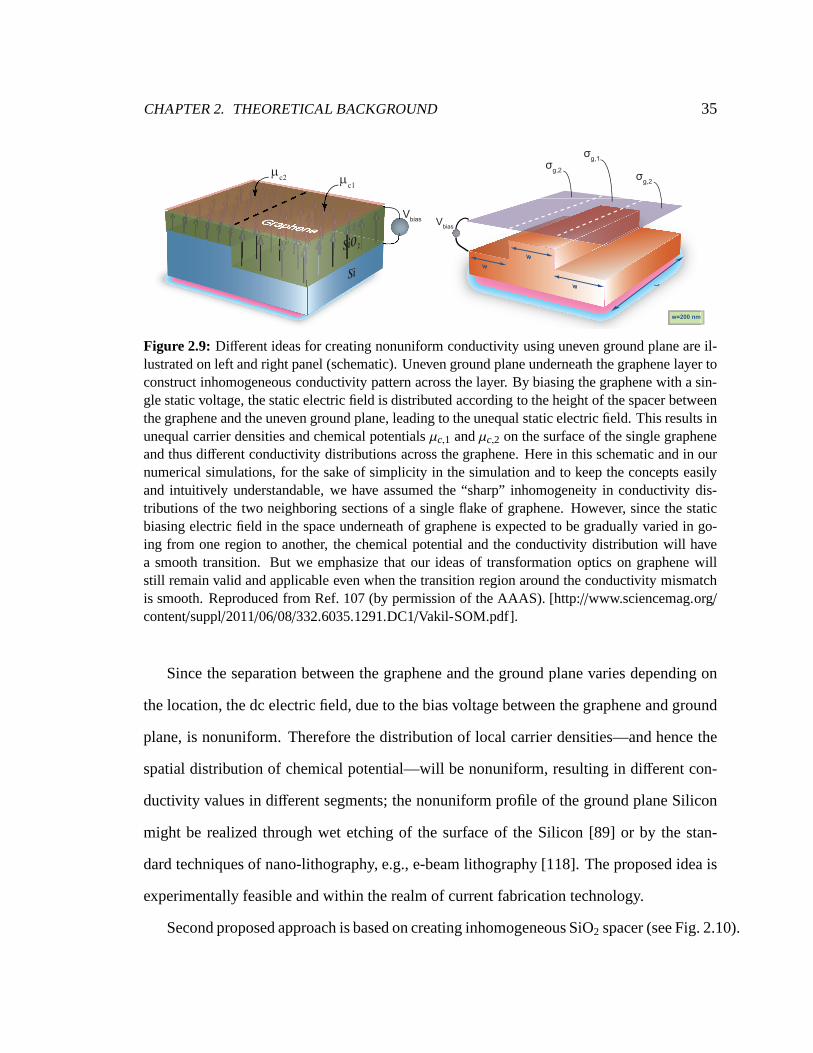
CHAPTER 2. THEORETICAL BACKGROUND 35
c1
c2
Vbias
w=200 nm
Vbias
g,2
g,2
g,1
Figure 2.9: Different ideas for creating nonuniform conductivity using uneven ground plane are il-lustrated on left and right panel (schematic). Uneven ground plane underneath the graphene layer toconstruct inhomogeneous conductivity pattern across the layer. By biasing the graphene with a sin-gle static voltage, the static electric field is distributedaccording to the height of the spacer betweenthe graphene and the uneven ground plane, leading to the unequal static electric field. This results inunequal carrier densities and chemical potentialsµc,1 andµc,2 on the surface of the single grapheneand thus different conductivity distributions across the graphene. Here in this schematic and in ournumerical simulations, for the sake of simplicity in the simulation and to keep the concepts easilyand intuitively understandable, we have assumed the “sharp” inhomogeneity in conductivity dis-tributions of the two neighboring sections of a single flake of graphene. However, since the staticbiasing electric field in the space underneath of graphene isexpected to be gradually varied in go-ing from one region to another, the chemical potential and the conductivity distribution will havea smooth transition. But we emphasize that our ideas of transformation optics on graphene willstill remain valid and applicable even when the transition region around the conductivity mismatchis smooth. Reproduced from Ref. 107 (by permission of the AAAS). [http://www.sciencemag.org/content/suppl/2011/06/08/332.6035.1291.DC1/Vakil-SOM.pdf].
Since the separation between the graphene and the ground plane varies depending on
the location, the dc electric field, due to the bias voltage between the graphene and ground
plane, is nonuniform. Therefore the distribution of local carrier densities—and hence the
spatial distribution of chemical potential—will be nonuniform, resulting in different con-
ductivity values in different segments; the nonuniform profile of the ground plane Silicon
might be realized through wet etching of the surface of the Silicon [89] or by the stan-
dard techniques of nano-lithography, e.g., e-beam lithography [118]. The proposed idea is
experimentally feasible and within the realm of current fabrication technology.
Second proposed approach is based on creating inhomogeneous SiO2 spacer (see Fig. 2.10).

CHAPTER 2. THEORETICAL BACKGROUND 36
Vbias
c1
c1
c2
Figure 2.10: (Schematic) Second idea to create inhomogeneous conductivity patterns acrossgraphene. Here several dielectric spacers with unequal permittivity functions can be used under-neath of the graphene to create unequal bias electric field distributions, resulting in inhomogeneouscarrier densities and conductivity patterns across layer of graphene. Reprinted from Ref. 107 (bypermission of the AAAS). [http://www.sciencemag.org/content/suppl/2011/06/08/332.6035.1291.DC1/Vakil-SOM.pdf].
Again applying a fixed dc voltage between the graphene and theground plane results
in a static electric field in this narrow region that is different from the static field elsewhere
in the spacer. This will alter the carrier density distribution and the segment of graphene
on top of this dielectric strip will have a different conductivity from other segments. If the
width of this strip on top of the spacer is small (but not too small to become comparable
with the nanostructured dimensions within a graphene, in which case the quantum nature of
the structure should be considered [104, 105]), the width ofthe graphene with the different
conductivity can be as small. It is worth mentioning that thedimensions we have chosen for
our examples are larger than the nanostructured dimensionswithin graphene, so the Kubo
conductivity model is still valid. Also, in our numerical simulations, for simplicity and to
keep the concepts easy to absorb, we have assumed a “sharp” inhomogeneity in conduc-
tivity distributions of the two neighboring sections of a single flake of graphene. Our ideas
of transformation optics will still be valid and applicableeven when the inhomogeneity

CHAPTER 2. THEORETICAL BACKGROUND 37
z
yx
Figure 2.11: Fresnel reflection for an SPP surface wave hitting a boundaryline due to conductivitymismatch in the plane of graphene. The darker region has different conductivity from the regionhighlighted with light gray. We investigate the reflection of the SPP surface wave that is launchedtoward the boundary created as result of conductivity mismatch.
between the two sections is not very sharp [107].
Now that we qualified graphene as a better platform for mid-IRmetamaterial struc-
tures and transformation optics devices, let us address theessential problems that form the
foundations for engineering such structures and devices.
2.2.2 Foundations for design of metamaterial structures and transfor-mation optics devices
As pointed out earlier our goal is to put forth graphene as a platform for metamaterials
and transformation optics. However to be able to design metamaterials and transformation
optical devices, it is most important to tackle four essential problems
(i) Propagation of SPP surface waves along graphene:This problem is basically what
we addressed above. We quantified the propagation parameters of a TM SPP surface
wave propagating along graphene, based on the surface conductivity model intro-

CHAPTER 2. THEORETICAL BACKGROUND 38
duced in section 2.1. We characterized the modes based on thesign of imaginary
part of conductivity and expressed dispersion relations for each mode in Eqs. (2.13)
and (2.14).
(ii) Green’s functions for an electric current source in the presence of graphene layer:
It is important to study the interaction of an electromagnetic dipolar source (e.g.,
atoms and molecules) with graphene. The fields can be derivedin terms of dyadic
Green’s functions represented using Sommerfeld integrals. This problem is a variant
of famous classic Sommerfeld half-plane and has been addressed in the literature by
several authors [41, 42, 72]. In the following sections we briefly discuss this problem,
review some of the relevant works and present the dyadic Green’s functions for TM
SPP surface waves.
(iii) Fresnel reflection:Another essential problem to address is the reflection of surface
plasmon-polariton (SPP) surface waves from boundaries in the plane of graphene. In
other words, we would like to ask the following question: if somehow a conductivity
mismatch is created within the graphene layer, how would an SPP surface wave reflect
from that boundary (see Fig. 2.11, in which two regions with differing conductivities
are shown in light and dark colors. The SPP surface wave is propagating iny-direction
toward the boundary of these two regions).
Due to 2-dimensional (2D) structure of graphene, derivation of an exact solution to
this problem proves to be complicated. The problem has been addressed in the context
of diffraction by surface impedance discontinuities and impedance half-planes [90].
However, in the following, we present a much simpler approximate semi-analytical
approach to quantify the reflection of SPP surface waves fromdiscontinuities in plane
of graphene.
CHAPTER 2. THEORETICAL BACKGROUND 39
(iv) Polarizability of a small patch that has different conductivity from the surrounding:
We are interested in the problem of scattering of SPP surfacewaves by a small patch
(for example a small disk) with a different conductivity from its surrounding host.
Once this problem is solved, in first-order approximation, we may regard any small
patch of graphene as a dipole moment with a known polarizability (which is related to
its geometrical and optical properties). Knowing the polarizability of the patch, since
we have also developed the Green’s functions for a current source in the proximity of
graphene, we are then able to obtain the fields scattered fromthe patch in the plane
of graphene layer. These patches will be building blocks of metamaterial structures
constructed based on graphene.
The problem of SPP propagation has already been addressed sowe devote next sections to
other three problems that form foundations for design and engineering metamaterials and
transformation optical devices.
2.2.3 Dydic Green’s functions for graphene
Efficient excitation of surface plasmon-polaritons on graphene is the precondition to any
optical metamaterial functionality we may envision based on this layer of carbon atoms.
One efficient way proposed to excite the SPP modes is to use quantum dots or molecules
or any other variant of quantum emitters [43, 54]. Describing such quantum emitters as
dipole moments, we can describe their bound modes due to presence of a graphene layer
using Green’s tensor. This problem is variant of classic Sommerfeld half-plane problem
with modified boundary conditions. Several researchers have addressed this problem [41,
42, 72]. Here we follow similar steps as Sommerfeld devised [46, 98] for the case of
horizontal dipole. The derivation for the vertical dipole is similar and we do not show the

CHAPTER 2. THEORETICAL BACKGROUND 40
z
yx
rh
!
p=py
x !
zz
yyyy
rrrhhhh
pppppppppppppppp=====pppppppppp=pppppppyyyppyyyy
Figure 2.12: Horizontal electric dipole alongy axis at distanceh above a graphene layer. Thegraphene layer is placed at the interface of two dielectric media, characterized by permittivitiesǫ1andǫ2, which in general can be lossy and dispersive.
steps, however we provide the results for an arbitrarily oriented dipole in terms of dyadic
Green’s functions [72].
Consider a horizontal electric dipolep = pyy (depicted in Fig. 2.12) in medium 1 (with
permittivity ǫ1 and permeabilityµ0). The graphene layer lies at the interface of the medium
1 and medium 2 (forz< 0 we have permittivityǫ2 and permeabilityµ0).
The fields can be described by Hertz vector potentialΠ, which satisfies Helmholtz
equation. At the first glance, it may appear reasonable to assume Hertz vector,Π, has
only y-component for a dipole aligned iny-direction. However to satisfy the boundary
conditions atz= 0, we need to have two components for Hertz vector. This can beresolved
by assuming Hertz vector also has a component alongz-direction
Π =(
0,Πy,Πz
)
. (2.29)
The electric and magnetic fields are related to Hertz vector as following (for n= 1, 2)
E(n)(r ) =(
k2n + ∇∇
)
Π(n)(r ), (2.30a)

CHAPTER 2. THEORETICAL BACKGROUND 41
H(n)(r ) = −iωǫn∇ ×Π(n)(r ), (2.30b)
in which kn = ω√µ0ǫn. Here we conduct the derivation for electric fields. Magnetic
fields can be obtained accordingly using Maxwell’s equations. In our case sinceΠx = 0,
Eq. (2.30a) can be simplified as (for n= 1, 2)
E(n)x =
∂
∂x∇ ·Π(n), (2.31a)
E(n)y = k2
nΠ(n)y +
∂
∂y∇ ·Π(n), (2.31b)
E(n)z = k2
nΠ(n)z +
∂
∂z∇ ·Π(n). (2.31c)
The Hertz potential vector can be written as
Π(1) = Πp +Π(1)s , (2.32)
for the first medium and
Π(2) = Π(2)s , (2.33)
for the second medium, whereΠp is the primary potential due to the dipole andΠ(1)s and
Π(2)s are the secondary potentials due to the presence of the graphene layer.
Forz> 0,Πy has to satisfy
(
∇2 + k21
)
Π(1)y = −
py
ǫ1δ(
r − r ′)
, (2.34)
and forz< 0(
∇2 + k22
)
Π(2)y = 0, (2.35)

CHAPTER 2. THEORETICAL BACKGROUND 42
Suppressing the multiplicative termpy
ǫ1and assumingp1,2 =
√
k2ρ − k2
1,2, the primary field
Πp,y is then given by
Πp,y =18π
∫ ∞
−∞H(1)
0 (kρρ)e−p1|z−h|kρdkρ
p1=
eik1r
4πr, (2.36)
whereH(1)0 (.) denotes the first kind Hankel function of zeroth order, andr =
√
ρ2 + z2. The
secondary fields can be written as following
Π(1)s,y =
18π
∫ ∞
−∞R(kρ)H
(1)0 (kρρ)e
−p1|z+h|kρdkρp1, (2.37)
Π(2)s,y =
18π
∫ ∞
−∞T(kρ)H
(1)0 (kρρ)e
p2z−p1hkρdkρp1, (2.38)
whereR(kρ) andT(kρ) are yet to be determined by satisfying the boundary conditions at
z= 0. Following an approach similar to Sommerfeld [98], using continuity of electric field
and boundary condition for tangential components of magnetic field (which include the
surface conductivity of graphene) atz= 0, we arrive at following relations
ǫ1Π(1)y = ǫ2Π
(2)y , (2.39a)
∂Π(1)y
∂y+∂Π
(1)z
∂z=∂Π
(2)y
∂y+∂Π
(2)z
∂z, (2.39b)
ǫ1Π(1)z − ǫ2Π(2)
z = −σg
iω∇ ·Π(1) = −
σg
iω∇ ·Π(2), (2.39c)
ǫ2∂Π
(2)y
∂z− ǫ1∂Π
(1)y
∂z= −σg
iωk2
1Π(1)y , (2.39d)
which are respectively obtained from continuity ofEy andEx, and boundary conditions for
Hy andHx. Denotingǫ2/ǫ1 by n, Eqs. (2.39a) and (2.39d) yield
1+ R(kρ) = nT(kρ), (2.40a)

CHAPTER 2. THEORETICAL BACKGROUND 43
np2T(kρ) − p1
(
1− R(kρ))
= iσgωµ0
(
1+ R(kρ))
. (2.40b)
Form Eqs. (2.40a) and (2.40b), one can obtain
R(kρ) =p1 − p2 + iωσgµ0
p1 + p2 − iωσgµ0, (2.41)
T(kρ) =2p1
n(
p1 + p2 − iωσgµ0
) . (2.42)
Equation (2.39b) can be recast as following
∂
∂y
(
Π(2)y − Π(1)
y
)
=∂
∂z
(
Π(1)z − Π(2)
z
)
(2.43)
But ∂Πy
∂y can be written as sinφ ∂Πy
∂ρ, whereρ =
√
x2 + y2 andφ = cos−1(ρ · x). As such and
from Eq. (2.43) it follows thatΠz must also have a sinφ factor, implying thatΠz must be
constructed from higher order Hankel functions (n = 1):
Π(1)z = sinφ
18π
∫ ∞
−∞H(1)
1 (kρρ)e−p1(z+h)Φ1(kρ)dkρ, (2.44)
Π(2)z = sinφ
18π
∫ ∞
−∞H(1)
1 (kρρ)ep2z−p1hΦ2(kρ)dkρ, (2.45)
Substituting Eqs. (2.36), (2.37), (2.38), (2.44) and (2.45) in Eq. (2.43), and considering
Eqs. (2.41) and (2.42), we obtain a system of linear equations which can be written in
following matrix form
p1 p2
− iωǫ1σg
p2 − iωǫ2σg
Φ1(kρ)
Φ2(kρ)
=2k2ρ
p1 + p2 − iωσgµ0
1n − 1
1n
. (2.46)
Solving forΦ1(kρ) andΦ2(kρ) yields
Φ1(kρ) = −2k2ρ
[
σgp2 − iωǫ2(
1− 1n
)]
[
σgp1p2 − iω (p2ǫ1 + p1ǫ2)] (
p1 + p2 − iωσgµ0
) , (2.47a)

CHAPTER 2. THEORETICAL BACKGROUND 44
Φ2(kρ) = −2k2ρ
[
−1nσgp1 − iωǫ1
(
1− 1n
)]
[
σgp1p2 − iω (p2ǫ1 + p1ǫ2)] (
p1 + p2 − iωσgµ0
) (2.47b)
Let us simplify the problem by assuming that graphene is freestanding in air (the case we
studied in previous sections) and we are looking at the case where the horizontal dipole is
rested on the graphene. This implies thatp1 = p2 = p =√
k2ρ − k2
0, ǫ1 = ǫ2 = ǫ0 and in turn
n = ǫ2ǫ1= 1, andh = 0. So we can simplifyR(kρ) andΦ1(kρ) as following
R(kρ) =iωσgµ0
2p− iωσgµ0, (2.48)
Φ1(kρ) = −2σgk2
ρ(
σgp− 2iωǫ0) (
2p− iωσgµ0
)
= −σgp
σgp− 2iωǫ0−
iωσgµ0
2p− iωσgµ0
= −σgp
σgp− 2iωǫ0− R(kρ), (2.49)
The total fields can be calculated using numerical evaluation of integrals on the original
Sommerfeld integral path (SIP) on the real axis, however thesurface waves field can be
evaluated analytically from the residue contribution of Sommerfeld integral; the pole sin-
gularities ofR(kρ) andΦ1(kρ) (Sommerfeld poles) represent discrete surface modes. The
pole ofR(kρ) (2p− iωσgµ0 = 0) yields the TE dispersion relation consistent with Eq. (2.14)
and the second pole singularity ofΦ1(kρ) (σgp−2iωǫ0 = 0) gives TM dispersion relation in
agreement with Eq. (2.13). These calculation are done by deforming the contour integral
and closing it in the upper half-plane of complexkρ. The poles then will be enclosed in the
contour and according to Cauchy’s principal value theorem we can compute the contribu-
tion due to the poles. As we are interested in TM modes due to the horizontal dipole, we
calculate the contribution due to the associated pole. AlsoΠy corresponds to TE surface
mode and does not contribute to the TM surface waves, but interestingly gives rise toΠz,

CHAPTER 2. THEORETICAL BACKGROUND 45
EyEy
z
y
x
p=pyŷ
-1 1[a.u.]
Figure 2.13: Distribution ofEy on the plane of a free-standing graphene due to a horizontal electricdipole on the graphene layer and aligned withy-axis.
which propagates mostly in the direction parallel to the dipole (φ = 90). As such in our
calculations we find the residue of the integral due toΠz. Conducting the calculations and
assumingpy
ǫ0= 1 (the term we dropped earlier) we obtain
ETM,SPPx (ρ, z) =
i sinφ cosφ8
p3[
H(1)0 (kρρ) − H(1)
2 (kρρ)]
e−p|z|, (2.50a)
ETM,SPPy (ρ, z) =
i sin2 φ
8p3
[
H(1)0 (kρρ) − H(1)
2 (kρρ)]
e−p|z|, (2.50b)
ETM,SPPz (ρ, z) =
i sinφ8
p2kρH(1)1 (kρρ)e
−p|z|, (2.50c)
The snapshot in time of distribution of real part of different components of electric field is
presented in Fig. 2.13 (Ey) and Fig. 2.14,A andB (Ex andEz). We can observe that the
mode is maximum in the direction of the dipole. The presence of graphene has substantially
changed the radiation pattern of the dipole. Similar derivation can be carried through to
obtain the TM SPP fields due to a vertical electric dipole (VED). Nikitn et. al [72] have

CHAPTER 2. THEORETICAL BACKGROUND 46
y
xp=pyŷ
Ez
B
y
xp=pyŷ
Ex
A
-1 1[a.u.] -1 1[a.u.]
Figure 2.14: The snapshot in time of distribution ofEx andEz on the plane of graphene due to ahorizontal electric dipole on the graphene layer and aligned with y-axis.
derived the closed form Green’s tensor for the TM SPP waves following methodology
developed in Ref. 77. They show that the Green tensor has the following form
↔G(ρ, z) ∝ e−p|z|
H(1)− (kρρ) 0 − iσgkρ
ωǫ0H(1)
1 (kρρ)
0 H(1)+ (kρρ) 0
− iσgkρωǫ0
H(1)1 (kρρ) 0 1
2
(
σgkρωǫ0
)2H(1)
0 (kρρ)
, (2.51)
whereH(1)± (.) = H(1)
0 (.) ± H(1)2 (.). Additionally authors offer an extensive analysis of the
dependence of the electric field strength (compared to free space radiation of the dipole) on
frequency and distance of the observation point from the surface [72]. Their study suggests
that for the frequency range and for the typical distances from the surface and away from
the dipole that are used in our studies in this thesis, it is safe to assume that the total electric
field, close to and on the surface, is dominated by the SPP surface wave electric field.
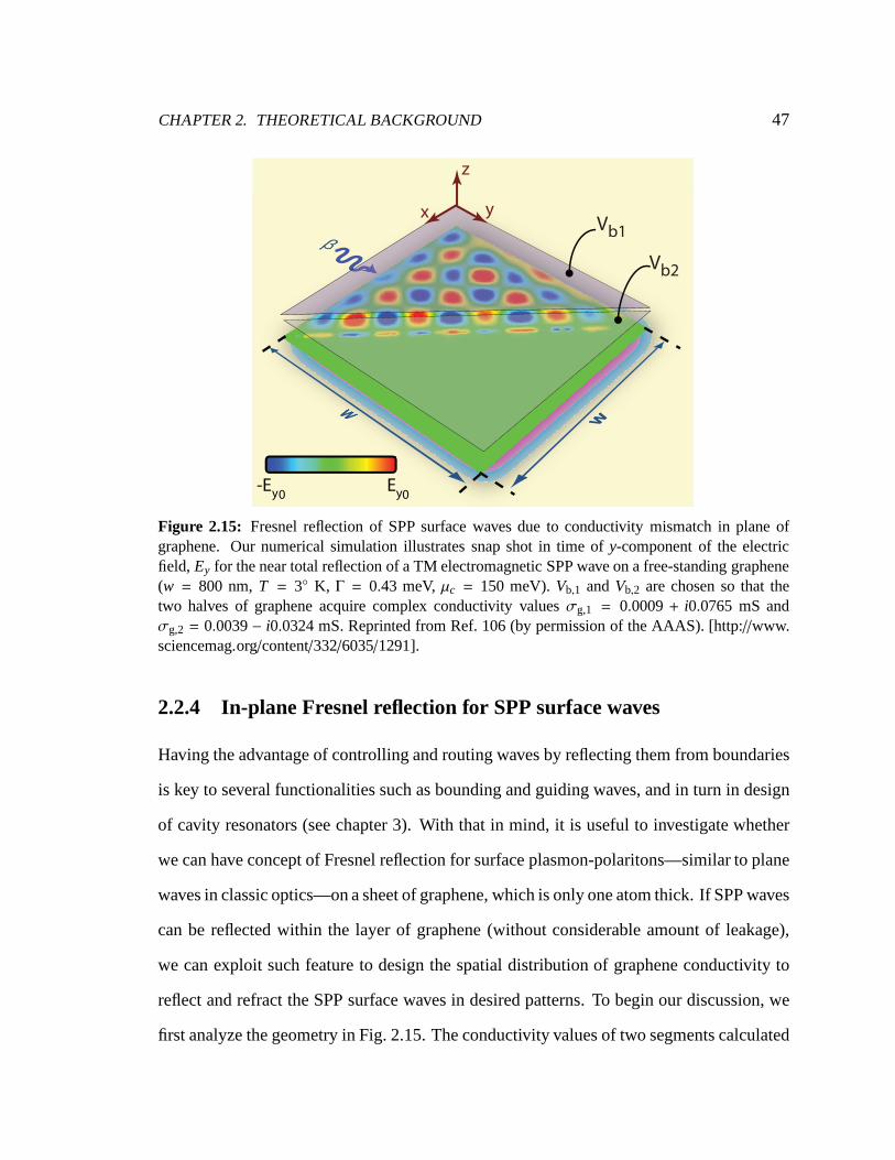
CHAPTER 2. THEORETICAL BACKGROUND 47
Vb1
z
Vb1
Vb2
yx
-Ey0
Ey0
Figure 2.15: Fresnel reflection of SPP surface waves due to conductivity mismatch in plane ofgraphene. Our numerical simulation illustrates snap shot in time of y-component of the electricfield, Ey for the near total reflection of a TM electromagnetic SPP waveon a free-standing graphene(w = 800 nm,T = 3 K, Γ = 0.43 meV,µc = 150 meV).Vb,1 andVb,2 are chosen so that thetwo halves of graphene acquire complex conductivity valuesσg,1 = 0.0009+ i0.0765 mS andσg,2 = 0.0039− i0.0324 mS. Reprinted from Ref. 106 (by permission of the AAAS).[http://www.sciencemag.org/content/332/6035/1291].
2.2.4 In-plane Fresnel reflection for SPP surface waves
Having the advantage of controlling and routing waves by reflecting them from boundaries
is key to several functionalities such as bounding and guiding waves, and in turn in design
of cavity resonators (see chapter 3). With that in mind, it isuseful to investigate whether
we can have concept of Fresnel reflection for surface plasmon-polaritons—similar to plane
waves in classic optics—on a sheet of graphene, which is onlyone atom thick. If SPP waves
can be reflected within the layer of graphene (without considerable amount of leakage),
we can exploit such feature to design the spatial distribution of graphene conductivity to
reflect and refract the SPP surface waves in desired patterns. To begin our discussion, we
first analyze the geometry in Fig. 2.15. The conductivity values of two segments calculated

CHAPTER 2. THEORETICAL BACKGROUND 48
from the Kubo formula forT = 3 K andΓ = 0.43 meV are, respectively,σg,1 = 0.0009+
i0.0765 mS andσg,2 = 0.0039− i0.0324 mS. The “farther” half section withσg,1 > 0
supports a TM SPP, whereas the “closer” half withσg,2 < 0 does not. Once a TM SPP
is launched in the farther-half section toward the discontinuity resulted from mismatch in
conductivities, it reflects back at that boundary line. Then, the incident and reflected waves
add up and form an oblique standing wave.
The reflection of SPP from this boundary line is analogous to the Fresnel reflection of a
plane wave from a planar interface between two mediums. Here, however, such reflection
occurs across a one-atom-thick platform, with a considerably little radiation loss owing to
high confinement of SPP to the graphene. This case might also be analogous to the Fresnel
reflection from a planar interface between a medium that supports propagating waves (for
example, a medium with a real refractive index, such as a dielectric) and another medium
that does not support propagating waves (for example, a medium with no real index, such
as a noble metal). Accordingly, on the graphene the Fresnel reflection of SPP results in a
near complete reflection [106]. The simulation results demonstrate an effective reflection
at the boundary line between the two segments.
In addition in Fig. 2.15 the simulation reveals a guided IR edge wave along the bound-
ary line between the two segments. This phenomenon might be related to the separation of
electrons and holes at the boundary region [13, 19, 20, 69]. Using an electron-holes liquid
model, Mishchenko et. al [69] show that for plasmon wavelengths smaller than the size
of charged domains, plasmon dispersion follows relationω ∝ β1/4|ρ0|1/4, whereρ0 is the
gradient of equilibrium charge density at the junction. In ageometrical optics framework,
Cserti et. al [19] interpret this p-n junction as a negative refractive index. We may conclude
that the second analogy described above is more laudable in explaining the physics behind
the observed edge mode. Figure 2.16 demonstrate numerical simulation of this edge wave,
which was excited using a horizontal dipole on the graphene and near the boundary of two

CHAPTER 2. THEORETICAL BACKGROUND 49
-Ey0
Ey0
w2=80 nm
Vb1
Vb2
xy
-Ey0
Ey0
w2=80 nm
Vb1
Vb2
xxyz
Figure 2.16: Distribution of Ey (snap shot in time) for a guided IR edge wave atf = 30 THz,supported along the boundary line between the two sections of the same sheet of graphene, whichhas two different conductivity regions (σg,1 = 0.0009+ i0.0765 mS,σg,2 = 0.0039− i0.0324 mS,L = 250 nm,w = 80 nm). Reprinted from Ref. 107 (by permission of the AAAS). [http://www.sciencemag.org/content/suppl/2011/06/08/332.6035.1291.DC1/Vakil-SOM.pdf].
regions. This special guided wave propagates along a “one-atom-radius” boundary line.
By post processing the simulation results, we estimate the wavelength of the guided edge
wave to be aroundλSPP= 61.5 nm.
Sounas & Caloz [99] show that such edge surface mode that propagates along the edge
of a graphene strip can be shorted using a PEC plate that is in the plane of the graphene
strip. They also find the dispersion curve for the edge mode with and without magnetic
bias.
A critical issue to address is how to quantify the reflection from the boundaries. Due
to special geometry of graphene (very small thickness), finding an exact solution to this
problem proves to be difficult. To study this problem, it might be possible to apply Wiener-
Hopf analysis, which solves problem of diffraction by surface impedance discontinuities
and impedance half-planes [90] but this analysis is cumbersome and may not provide much

CHAPTER 2. THEORETICAL BACKGROUND 50
insight into the problem. For practical purposes it might suffice to find an approximate
solution, as by employing powerful computational resources available these days, one can
always optimize any design based on first-order approximations. We have developed a
simple semi-analytical approach based on a transmission-line (TL) analogy to quantify the
reflection of SPP surface waves from discontinuities in plane of graphene.
We address normal incidence here. The case of oblique incidence can follow from the
same analogy by proper modifications. Consider a graphene layer that has two segments
with two different conductivity values (one may utilize any of the methods we proposed
earlier to realize such nonuniformity in conductivity pattern). The reflection from edge
of the second segment within the graphene layer might be analog of reflection from a
“lumped” impedance terminating a transmission line. Figure 2.17 illustrates the analogy.
Based on this analogy we can decompose the transverse component of the electric field
(Ez) into two components: a forward traveling wave and a backward traveling wave which
is reflected from the edge of graphene (or in our transmissionline analogy from the ter-
minating impedance). Suppose that the forward wave (traveling alongy-direction) has the
form Ez,0eiβy, whereβ is the propagation constant (or complex wavenumber alongy). The
backward electric field will be of formREz,0e−iβy, whereR is the reflection coefficient due
to the second region (or equivalently from the load at the endof the impedance). Writing
the complex reflection coefficient asR = ρeiθ, we can obtain the total transverse electric
field just above the plane of graphene (say small distanceδ) as follows
Ez = Ez,0e−pδ
(
eiβy + ρeiθeiβy)
, (2.52)
where as beforep =√
β2 − k20. Noting thatβ = βr + iβi, Eq. (2.52) can be recast as
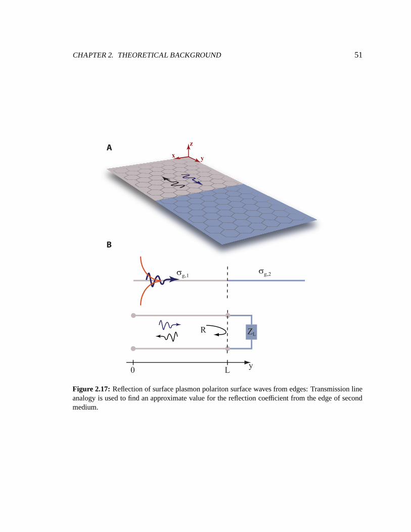
CHAPTER 2. THEORETICAL BACKGROUND 51
z
yx
g,1 g,2
ZLR
y0 L
A
B
Figure 2.17: Reflection of surface plasmon polariton surface waves from edges: Transmission lineanalogy is used to find an approximate value for the reflectioncoefficient from the edge of secondmedium.

CHAPTER 2. THEORETICAL BACKGROUND 52
following
Ez = Ez,0e−pδ
[(
e−βiy cosβry+ ρeβiy cos(θ − βry)
)
+i(
e−βiy sinβry+ ρeβiy sin(θ − βry)
)]
. (2.53)
We can obtain total field by solving Maxwell’s equations using full-wave numerical simu-
lations. Separating the transverse (y-component) of the electric field, we then find a set of
parameters (Ez,0, βr, βi, ρ, θ) in Eq. (2.53) such that the curve described by this equationis
fitted to the real and imaginary parts of numerical data points obtained from simulation. We
find the optimal set of parameters by simultaneously minimizing the sum of square errors
(SSE) between real and imaginary parts of data points from the equation and numerical
simulations. Finally having values ofρ andθ, we can determine the complex reflection
coefficient.
As a simple scenario, to illustrate how we can find the reflection coefficient from the
edges, consider a graphene layer that is infinite inx-direction—meaning that there is no
variation of the field inx-direction—and has finite lengthL in y-direction (Fig. 2.18). In
the transmission line analog the graphene is described as a transmission line, whose end is
left open to air. Simulation parameters are as usual (µc = 150 meV andΓ = 0.43 meV) and
frequency of operation is 30 THz. The layer is long enough to support multiple wavelengths
of SPP surface waves. We consider a long structure to ensure that at the locations along
the graphene layer where we fit our data points, the possible higher order electromagnetic
modes due to edges have died out and do not affect our calculations. The distribution of
the transverse electric field from numerical simulations isshown in Fig. 2.18.
Since the geometry and the fields are uniform inx-direction, we only need to fit the data
points (real and imaginary parts) along an arbitrary line parallel to y axis (we have chosen
y axis). Also in this process sinceδ (distance from plane of graphene) is very small,e−pδ
term is suppressed and its effect is absorbed inEz,0. As explained earlier we solve for a

CHAPTER 2. THEORETICAL BACKGROUND 53
y
x
z
0 1[a.u]
1.45 m
Figure 2.18: Study of reflection of SPP surface waves from edges. Based on our TL analogy we canregard the reflection from the edge of graphene as reflection from an open-ended transmission line.In the similar manner we can define impedance for such radiation we can do so for the radiationfrom the edge. The graphene layer has conductivityσg,1 = 0.0009+ i0.0765 mS. The magnitude ofthe transverse component of the electric field (Ez) is shown onx-y andy-z planes.
set of parameters (Ez,0, βr, βi, ρ, θ) in Eq. (2.53) such that the SSE [difference between data
points obtained using simulations and using correspondingdata points based on Eq. (2.53)]
is minimized. Implementing this procedure, we arrive at theresults displayed in the second
row of table 2.1 (in implementing the procedure, without loss of generality, we assume
Ez,0 = 1 and as such here we did not report this value).
Table 2.1: The set of parameters obtained from fitting numerical data toEq. (2.53) for first twoscenarios (see text).
Scenario ρ θ βr/k0 βi
µc,1 = 150 meV – air 0.8243 2.1027 69.77 1.05× 10⁻⁴
µc,1 = 150 meV –µc,2 = 65 meV 0.6825 1.4074 70.06 9.05× 10⁻⁵
Second scenario is similar to panelA from Fig. 2.17. Here the distribution of chemical
potential of graphene layer is assumed to be non-uniform andtwo regions with two different
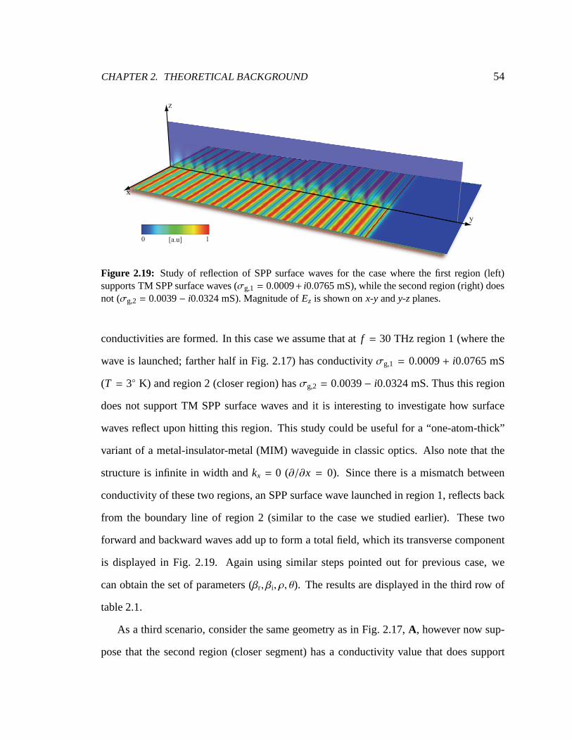
CHAPTER 2. THEORETICAL BACKGROUND 54
y
x
z
0 1[a.u]
Figure 2.19: Study of reflection of SPP surface waves for the case where thefirst region (left)supports TM SPP surface waves (σg,1 = 0.0009+ i0.0765 mS), while the second region (right) doesnot (σg,2 = 0.0039− i0.0324 mS). Magnitude ofEz is shown onx-y andy-zplanes.
conductivities are formed. In this case we assume that atf = 30 THz region 1 (where the
wave is launched; farther half in Fig. 2.17) has conductivity σg,1 = 0.0009+ i0.0765 mS
(T = 3 K) and region 2 (closer region) hasσg,2 = 0.0039− i0.0324 mS. Thus this region
does not support TM SPP surface waves and it is interesting toinvestigate how surface
waves reflect upon hitting this region. This study could be useful for a “one-atom-thick”
variant of a metal-insulator-metal (MIM) waveguide in classic optics. Also note that the
structure is infinite in width andkx = 0 (∂/∂x = 0). Since there is a mismatch between
conductivity of these two regions, an SPP surface wave launched in region 1, reflects back
from the boundary line of region 2 (similar to the case we studied earlier). These two
forward and backward waves add up to form a total field, which its transverse component
is displayed in Fig. 2.19. Again using similar steps pointedout for previous case, we
can obtain the set of parameters (βr, βi, ρ, θ). The results are displayed in the third row of
table 2.1.
As a third scenario, consider the same geometry as in Fig. 2.17, A, however now sup-
pose that the second region (closer segment) has a conductivity value that does support

CHAPTER 2. THEORETICAL BACKGROUND 55
TM SPP waves. Addressing this type of reflection (where two media do support prop-
agating modes) could form foundations for design of waveguides based on total internal
reflection—similar to a optical fiber waveguide where core and cladding both support light
modes, but due to total internal reflection of light-waves, the mode remains bounded in the
core region. One subtle issue here is that the reflection coefficient obtained based on the
forward and backward wave in the first region is not simply dueto reflection from second
region conductivity mismatch, but also due to the effect of the mismatch and reflection from
the edge of the second region; there is a propagating forwardmode in the second region,
reflecting from the edge of this region. The reason we cannot suppress this reflection from
edge is that design of perfect absorbing wall is a challenging task in our geometry (as we
will discuss in appendix B we have attempted to resolve this issue by redesigning concept
of Salisbury sheet for a TM SPP mode on graphene, but this absorbing boundary condition
does not work perfectly, so we do have some reflection, albeitsmall, from the edges if we
use this absorbing boundary conditions).
Consequently we decided to add a third region at the end of thesecond region, whose
imaginary part of conductivity is negative, so it does not support SPP surface waves. As
such there will not be any propagating modes in the third region and we do not need to
be concerned about reflection in this region, as modes die outbefore reaching the edge of
the graphene layer (this as well is the case for the second scenario discussed above). By
finding reflection from region 2 in region 1 and from region 3 inregion 2, we can back
out the reflection in region 1 due to only region 2 (as if the second region was extended to
infinity in y-direction, so there was no backward wave). In order to retrieve this reflection
coefficient, we again exploit a transmission line analogy as depicted in bottom panel of
Fig. 2.20. If we respectively denote the individual reflection from region 2 in region 1 –
due toonly mismatch– and reflection from region 3 in region 2 asΓ12 andΓ23, then the
total reflection (due to both mismatch and reflection from edge of third medium),Γin can

CHAPTER 2. THEORETICAL BACKGROUND 56
be obtained from following equation [7, 17]
Γin =Γ12 + Γ23ei2β2d
1+ Γ12Γ23ei2β2d, (2.54)
whered is length of the second region (in this exampled = 1.8 µm andβ2 ≈ 30k0). Γ12,
which is only due to mismatch of conductivities (as if we had two semi-infinite sheet of
graphene with conductivitiesσg,1 andσg,2), can be computed from Eq. (2.54) in terms of
Γin andΓ23, which could be obtained from our numerical simulations
Γ12 =Γ23ei2β2d − Γin
ΓinΓ23ei2β2d − 1. (2.55)
To computeΓin andΓ23 using numerical simulations, we repeat the same steps as before
in fitting data points to find the optimal set of parameters forEq. (2.53). The results are
reported in second and third rows of table 2.2. Using these values from table 2.2 and
Eq. (2.55), we find individual reflection coefficient due to region 2 to be≈ 0.47eiπ/2.
Table 2.2: The set of parameters obtained from fitting numerical data toEq. (2.53) for third scenarioscenarios (see text).
Scenario ρ θ βr/k0 βi
µc,1 = 150 meV –µc,2 = 300 meV 0.6070 0.4417 72.30 4.31× 10⁻⁴
µc,1 = 300 meV –µc,2 = 65 meV 1.00 0.4561 30.47 1.59× 10⁻⁴
As one last point in this part we would like to distinguish between reflection from
the plane of graphene and in-plane reflection of SPP surface waves propagating along a
graphene layer with nonuniform conductivity (for example Fig. 2.17). These are two com-
pletely different problems. In this section we addressed the latter as itis what we need in
our paradigm of “one-atom-thick” optical metamaterials and transformation optics. The
former problem has been addressed by others [27, 41]‖. We would like to also note that
‖It can be shown that for normal incidence the reflection from agraphene layer with complex surfaceconductivityσg is R=
σgη0/21+σgη0/2
and transmission coefficient isT = 1+ R.

CHAPTER 2. THEORETICAL BACKGROUND 57
z
yx
ZLZ1, 1 Z2, 2
Zin
!g,1
!g,2
!g,3
|Ez|
0 1[a.u]
d1 d2
Figure 2.20: Study of reflection of SPP surface waves for the case where both regions support TMSPP surface waves (σg1,i, σg2,i > 0). Magnitude ofEz is shown on they-z plane. Bottom paneldepicts the transmission line analog of the geometry (d1 ≈ 2.2 µm, d2 ≈ 1.8 µm).
the problem of reflection from plane of graphene is a rich and interesting area by itself and
several ideas may follow from that study. For example Sounas& Caloz [100], theoretically,
and Crassee et. al [18], experimentally, have studied reflection from a graphene layer under
magnetic bias and observed that the geometry under study canexhibit a broadband elec-
tromagnetic nonreciprocity and gyrotropic behavior (Faraday rotation), which can serve as
basis for design of magneto-optical devices such as nonreciprocal phase shifters.
2.2.5 Scattering from subwavelength graphene patches
As mentioned in chapter 1, metamaterials are artificial structures that mimic physically re-
alizable response functions and they are usually constructed by embedding subwavelength
inclusions or inhomogeneities in a host medium. Thus it is ofparticular significance to
describe behavior of such inclusions or inhomogeneities, as their collective behavior forms
the total optical response function of the medium. Addressing this problem is essentially
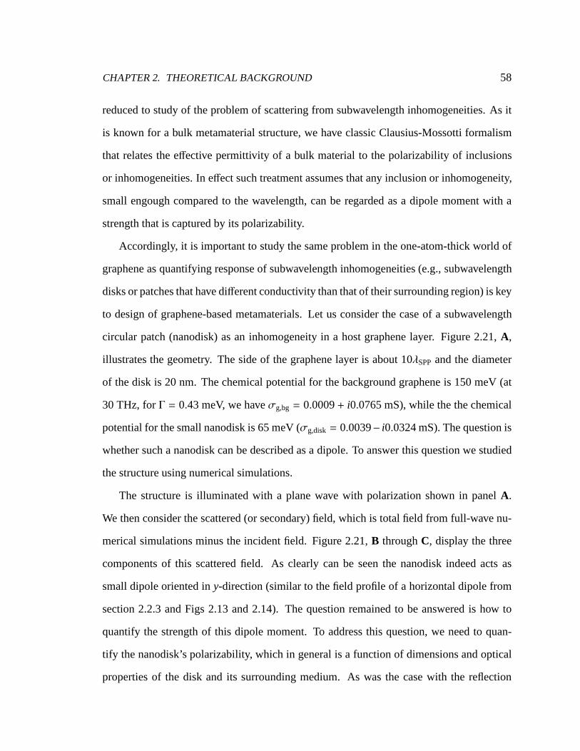
CHAPTER 2. THEORETICAL BACKGROUND 58
reduced to study of the problem of scattering from subwavelength inhomogeneities. As it
is known for a bulk metamaterial structure, we have classic Clausius-Mossotti formalism
that relates the effective permittivity of a bulk material to the polarizability of inclusions
or inhomogeneities. In effect such treatment assumes that any inclusion or inhomogeneity,
small engough compared to the wavelength, can be regarded asa dipole moment with a
strength that is captured by its polarizability.
Accordingly, it is important to study the same problem in theone-atom-thick world of
graphene as quantifying response of subwavelength inhomogeneities (e.g., subwavelength
disks or patches that have different conductivity than that of their surrounding region) is key
to design of graphene-based metamaterials. Let us considerthe case of a subwavelength
circular patch (nanodisk) as an inhomogeneity in a host graphene layer. Figure 2.21,A,
illustrates the geometry. The side of the graphene layer is about 10λSPPand the diameter
of the disk is 20 nm. The chemical potential for the background graphene is 150 meV (at
30 THz, forΓ = 0.43 meV, we haveσg,bg = 0.0009+ i0.0765 mS), while the the chemical
potential for the small nanodisk is 65 meV (σg,disk= 0.0039− i0.0324 mS). The question is
whether such a nanodisk can be described as a dipole. To answer this question we studied
the structure using numerical simulations.
The structure is illuminated with a plane wave with polarization shown in panelA.
We then consider the scattered (or secondary) field, which istotal field from full-wave nu-
merical simulations minus the incident field. Figure 2.21,B throughC, display the three
components of this scattered field. As clearly can be seen thenanodisk indeed acts as
small dipole oriented iny-direction (similar to the field profile of a horizontal dipole from
section 2.2.3 and Figs 2.13 and 2.14). The question remainedto be answered is how to
quantify the strength of this dipole moment. To address thisquestion, we need to quan-
tify the nanodisk’s polarizability, which in general is a function of dimensions and optical
properties of the disk and its surrounding medium. As was thecase with the reflection

CHAPTER 2. THEORETICAL BACKGROUND 59
eh
k
xy
z
EzEy
Ex
A B
DC
y
x
y
x
y
x
-1
1
[a.u]
Figure 2.21: Scattering of SPPs by a nanondisk.A Geometry of problem: a subwavelength diskwith a different conductivity from conductivity of the host graphene.The structure is illuminatedwith a plane-wave from top. The nanodisk (r = 10 nm), acts as dipole.B throughD show the snap-shot in time of different components of the secondary (i.e., scattered) electric field due to the patch;the incident field has been removed from the total field calculated from numerical simulations. Thefields due to the nanodisk mimics the fields of a dipole. The issue is how to find the polarizabilityof such nanodisk as function of its dimensions and optical properties.

CHAPTER 2. THEORETICAL BACKGROUND 60
problem (see section 2.2.4), full-analytical treatment ofthe problem might not be straight-
forward if not impossible. There have been some studies on how light scatters from a small
hole in a thick metal film [91] such as gold, however again verythin structure of graphene
makes such studies almost obsolete in this case. Thongrattanasiri et. al [103] have sug-
gested that polarizability of a small subwavelength graphene disk follows a resonance that
has a Lorentzian line shape
α(ω) =3c3κr
2ω2p
1ω2
p − ω2 − iκω3/ω2p
, (2.56)
whereωp is the plasmon frequency,κ is the decay rate, andκr is the radiative component
of κ. Then using full-wave numerical simulations the fitting parametersκ, κr andωp can
be determined. These parameters implicitly bear the dependence on the dimensions and
optical properties of the nanodisk.
In addition, using full-wave simulations, we obtain the polarizability of a circular patch
as a function of its radius. The simulations are performed for f = 30 THz, at which the
circular patch has conductivityσg,disk = 0.0039− i0.0324 mS (µc = 65 meV) and the
background conductivity isσg,bg = 0.0014− i0.1787 (µc = 300 meV). To find the dipole
polarizability of the disks, the radius of the circular patch is varied from 2 nm to 20 nm
and the magnitude and phase of the scattered electric field (|Einc| = 1) due to the disk is
compared with a deeply subwavelength dipole source with dipole momentp = 1 (in our
simulation we assumed the length of the dipole source is 2 nm). We do realize that these
length scales are not realistic, however we wanted to make sure that the diameter of the
disks are indeed subwavelength (with respect toλSPP, which in this scenario is≈ 336 nm).
The results are shown in Fig. 2.22. As expected, the magnitude of the polarizability in-
creases with the size of the disk (roughly∝ a3). In addition, the higher the conductivity
contrast between the disk and the background, the larger thepolarizability of the disk.

CHAPTER 2. THEORETICAL BACKGROUND 61
10 15 202
4
6
8
10x 10
33
a (nm)
!
10 15 20
2.6
2.8
3
3.2
a (nm)
Arg
[!]
(Rad
)
Figure 2.22: Polarizability of graphene nanondisk as a function of its radius (right panel: magni-tude, left panel: phase angle).
Graphene antennas
The problem of scattering from subwavelength patches is thecritical to study of several
other problems. For example we just showed a single patch of graphene can effectively act
as an emitter within graphene, suggesting such entity couldbe employed as an antenna to
receive and transmit signals in and out of the graphene layer. To show coupling efficiency
of the SPP using the graphene patch, we use a quantity called coupling cross sectionσc
defined asPrecSinc
, wherePrec is the power received by the patch andSinc is the incident power
per unit area. Our calculation indicate that this subwavelength patch has a coupling cross
section more than 4 times its geometrical area (we obtained almost the same value for a
hole of the same size instead of the patch). This quantity depends on the shape, dimensions
and conductivity of the patch and conductivity of the surrounding medium, so creating high
contrast between the conductivity of the patch and that of the background graphene should
result in larger coupling cross sections. This could be subject of further study.
The possibility of inclusions as antennas has been examinedexperimentally by Zhou et.
al [120]; they show that surface plasmons can be enhanced even locally and at the atomic

CHAPTER 2. THEORETICAL BACKGROUND 62
scale using point defects. Their study indicates that a single point defect (which is created
by using dopant atoms such as boron, nitrogen, iron, silver of gold) can act as an “atomic
antenna” in the petahertz region. There has been some numerical studies similar to what
presented here (see Ref. 62)∗∗.
2.2.6 Coupling between an emitter and graphene SPPs: Enhancedlight-matter interaction
In section 2.2.3 we studied the solutions to Maxwell’s equations in the presence of graphene
and also how graphene can change radiation pattern of an emitter in free-space. We ob-
served that presence of graphene can give rise to surface plasmon polariton waves at the
surface, which are much stronger than the fields due to an emitter in free-space.
Before Purcell’s study in 1946, spontaneous emission of an atom or molecule was
deemed as an intrinsic property of such entity. But his work suggested that the environ-
ment surrounding an atom or molecule can alter radiative characteristic of the atom or
molecule. There have been some studies on the strength of coupling of quantum emit-
ters and graphene surface plasmon-polaritons. These studies predict high decay rates for
such quantum emitters in the proximity of the homogeneous and inhomogeneous graphene
layer [43, 54]. Koppens et. al [54] propose that due to this high decay rate (spontaneous
emission rate), graphene can be a new platform for enhanced light-matter interaction. They
study the problem in a quantum optical context. We briefly discuss some of the theoreti-
cal concepts underlying their study as they closely relate to our work on graphene-based
cavities in chapter 3. In chapter 3, we treat the problem of cavity classically and try to
analyze the cavity response using circuit models for resonance. In our framework, there is
∗∗Another interesting scenario in which scattering problem find importance is the inverse scattering fromobjects within graphene layer. As we point out very briefly inchapter 5, inverse scattering problem is ofimmense significance in tomography applications using graphene—e.g., in imaging of a rough surface.

CHAPTER 2. THEORETICAL BACKGROUND 63
an analogy between the quantum and the classical view of the problem. We will see how,
in such framework, decay rate of a quantum emitter can be regarded as a resistive part of
impedance of an antenna [35].
The spontaneous emission rateγ of a the dipole can generally be obtained using Fermi’s
golden rule [77] by considering the combined “field+ system” states in terms ofpartial
local density of states†† of the dipoleρp(r0, ω0),
γ =2ω0
3~ǫ0|p|2ρp(r0, ω0), (2.57)
in which r0 is the location of dipole,ω0 is the transition frequency andp is the dipole
moment of the atom or molecule (this discussion is based on the assumption that our dipole
can be described as a two-level quantum system). The densityof states is related to Green’s
tensor of the dipole at the location of dipole:
ρp(r0, ω0) =6ǫ0πω0
[
p · ℑ↔G(r0, r0;ω0) · p
]
, (2.58)
wherep is p|p| and
↔G(r0, r ;ω0) is the Green’s tensor at the location of dipoler0 due to the
dipole itself—the electric field at locationr due to the dipole isE(r ) =↔G(r0, r ) · p. For
free-space the decay rateγ0 of the dipole will take the simple following form
γ0 =ω3
0|p|23πǫ0~c3
. (2.59)
An important quantity that captures the effect of environment on the rate of spontaneous
emission of an emitter isPurcell factor, defined as the total decay rate of the emitter nor-
malized to the free-space decay rate. It can be shown that this quantity only depends on the
scattered field due to the inhomogeneous environment [77]
Fp =γ
γ0= 1+
6πǫ0|p|2
1
k30
ℑp · Es(r0) , (2.60)
††Partial local density of states is defined as number of modes per unit volume and frequency at the originof the quantum system

CHAPTER 2. THEORETICAL BACKGROUND 64
whereEs(r0) is the scattered field at the location of the dipole. In Eq. (2.60) interaction
betweenEs andp is assumed to be weak. Also it has been assumed that the decay rate is
purely radiative.
Now let us briefly discuss the connection between classic andquantum picture of the
problem. As we know from classical point of view, according to Poynting’s theorem, for
anysourceor sinkcurrent distributionj in a linear medium, the rate of energy dissipation
dW/dt should be equal to power radiated by that source [77]
dWdt= −1
2
∫
Vℜj ∗ · EdV. (2.61)
Thus for a dipolej (r ) = −iω0pδ(r − r0), we can write
dWdt=ω0
2ℑp∗ · E(r0), (2.62)
whereE(r0) is electric field due to the dipole at its own location. This equation can be
written in terms of Green’s tensor as
dWdt=ω2
0|p|22
[
p · ℑ↔G(r0, r0;ω0) · p
]
. (2.63)
The connection between two point of views becomes clear by comparing combination
of Eqs. (2.57) and (2.58) with Eq. (2.63). We will come back tothis analogy later in
chapter 3, where we talk about one-atom-thick cavity resonators using graphene. There we
use classic electrodynamics to analyze the problem of cavity resonator (i.e., by considering
quantities such as Q-factor, mode-volume) and try to present a circuit equivalent for the
cavity resonator. The decay rate of the system will be closely related to the resistive part of
impedance introduced for the two-level system [35].
2.2.7 Excitation of graphene surface plasmon-polaritons
As discussed in sections 2.2.3 and 2.2.6, one efficient way of exciting surface plasmon-
polaritons in graphene is to use a quantum emitters such as anatom or molecule resonat-

CHAPTER 2. THEORETICAL BACKGROUND 65
e
h
kSPP
SPP
z
yxA
10-2 1[a.u]
z
B
y
Figure 2.23: Excitation of SPPs using diffraction grating. All fields shown here are the scatteredcomponent; the incident component is removed. PanelA shows the geometry of the graphene layer,the diffraction grating and polarization of incident field. PanelB illustrates the magnitude of thescattered field ony-zplane.
ing at the desired wavelength. In this section, we investigate other possibilities to excite
graphene SPP modes. The central notion here is to excite these modes using a plane wave.
Due to high confinement of the SPP surface waves, coupling in and out of graphene is very
challenging. In addition, as we will see here, with conventional techniques of coupling
light with SPP surface waves, the efficiency is undesirably low.
Excitation of surface plasmon-polaritons using diffraction grating
One method for excitation of SPPs is similar to diffraction grating structure in conventional
optics (see Fig. 2.23,A). Suppose that a graphene layer withµc = 150 meV (T = 3 K,
Γ = 0.43 meV) is standing in free space, while ten silver nanorods (r ≈ 8 nm), distanced
λSPP≈ 144 nm from each other, are placed underneath and very close to the graphene (in

CHAPTER 2. THEORETICAL BACKGROUND 66
a real setup the nanorods can be embedded in the spacer, upon which graphene is rested;
the physical mechanism underlying the problem will remain unaffected). A plane wave
launched from the top toward the graphene layer (which, in our simulations, is 50λSPPlong
in y-direction and infinite inx-direction, i.e.∂/∂x = 0), will induce dipole moment in the
nanorods and the since the these nanorods are separated byλSPP, the fields due the dipole
moments add up in phase, giving rise to SPP surface waves in the graphene layer. We
studied this structure numerically by full-wave simulation of total field (which is sum of
incident plane wave field and secondary field formed by scattering from graphene+ grat-
ing system) and removing the incident component to obtain the scattered (secondary) field.
Figure 2.23,B, illustrates the magnitude of scattered field on they-z plane. From this sim-
ulation we can clearly observe the SPP mode and how it is confined to the graphene layer.
Unfortunately, with this geometry the coupling efficiency is as low as∼ 0.1%. Since radius
of the wires is very small, the dipole moment induced in the nanorods is extremely small,
resulting in this weak coupling. As expexted efficient coupling to graphene’s extremely
confined SPP surface waves is a challenging task; for examplemerely increasing the diam-
eter of the nanorods does not result in considerably more effective coupling; for example
increasing the radius from 8 nm to 35 nm, leads to a coupling efficiency of∼ 0.55%, which
is still very small. As we will point out in the follwoing section (see Remark in subsec-
tion 2.2.7), to achieve larger coupling, one needs to exploit techniques that are based on
mechanisms different from those employed conventionally.
Excitations of surface plasmon-polaritons using array of patches
Based on the discussion in section 2.2.5, here we propose another way of coupling to
graphene SPPs. Using arrays of circular patches, we might beable to achieve higher cou-
pling efficiency. For example consider the geometry in Fig. 2.24,A, where the background

CHAPTER 2. THEORETICAL BACKGROUND 67
B
A
e
h
k
xy
y
z
z
S
Figure 2.24: Excitation of SPPs using array of subwavelength disks. Panel A shows the geometryand distribution of the vectorial scattered electric field on they-zplane (snap shot in time). PanelBillustrates the Poynting’s vector of the SPP surface wave ony-z plane.
graphene has conductivity with positive imaginary and patches conductivity has negative-
valued imaginary parts (conductivity values are the same aswhat used throughout this
thesis). In our simulation the radius of each patch is 10 nm and we assumed that the two
arrays are separated byλSPP in the longitudinal direction while they areλSPP/5 apart from
each other in lateral direction. The patches act as antennasand when the structure is illu-
minated with a plane wave, one can couple photons to the SPP modes of graphene through
these patches. With this geometry and only two rows of these arrays, we achieved coupling
efficiency of∼ 0.6%, which is still small but larger than the grating structure proposed ear-
lier. By changing shape and dimension, and by increasing number of arrays, we might be
able to achieve larger coupling. Figure 2.24,A, illustrates the electric field of SPP surface
wave coupled using this technique on they-zplane (the structure is uniform inx-direction).
Figure 2.24,B, shows the Poynting vector of the SPP wave. It is clear that the power is
confined around the graphene layer.

CHAPTER 2. THEORETICAL BACKGROUND 68
p=pyŷ
z
x y
z
yx
0 1[a.u]
Figure 2.25: A horizontal dipole on top of a uniform graphene layer withµc = 300 meV. Thedistance of dipole from graphene is 200 nm. The inset shows the geometry under study. ThePoynting vector (strength shown in gray scale) is superimposed on top of the density plot of theelectric field intensity.
Remark:As we just observed both techniques described above result in very low cou-
pling efficiencies, but studies have shown that an emitter in close proximity of a graphene
layer can couple efficiently to plasmon modes of graphene (see Ref. 43 for example). Fig-
ure 2.25 shows numerical simulation of electric field and Poynting vector due to a horizon-
tal dipole near surface of graphene layer with uniform chemical potentialµc = 300 meV.
As can be seen from Fig. 2.25, the total field is combination oftwo main components:
dipole radiation field and SPP field. Based on the numerical simulation of our geometry,
roughly 80% of the dipole power couples to dipole radiation fields, while the rest radiates
into SPP waves (i.e., assuming all the energy loss of the source is associated with radiation,
PSPPPrad=γSPP
γrad= 1
4). However Huidobro et. al have shown that, under certain conditions, in
principle the total decay rateγ can become almost equal to the surface plasmons decay rate
γSPP [43], implying that most of the emitter’s power can radiate into SPP. So why do we
observe such a small coupling in the techniques proposed above? The reason can be at-
tributed to inefficient coupling between the plane wave and the scatterers, i.e., the nanorods
in the first proposal and patches in the second proposal. In other words, as we mentioned
CHAPTER 2. THEORETICAL BACKGROUND 69
earlier the dipole moments induced by the plane wave in the scatterers are extremely small,
resulting in small amount of power radiating from the scatterers into the dipole radiation
and SPP fields, so no matter how large is the coupling efficiency between the scatterers and
graphene plasmons, the amount of power radiated into plasmons is small compared with
incident power (i.e., power of the incident plane wave). To tackle this issue somehow the
Poynting vector has to, as much as possible, be directed toward the scatterers, enabling
larger interaction between particle and the plane wave.
Suppose for example that the emitter is a spherical subwavelength nanoparticle. It is
well known that if the particle becomes resonant the scattering cross section of the particle
can exceed several multiples of the particle’s actual crosssection (for a spherical nanopar-
ticle for example typical values for scattering cross section is multiples ofλ2
02π ). It has been
shown that by proper design of a plasmonic-dielectric-plasmonic layered structure, in prin-
ciple, an arbitrarily large total cross section can be achieved [92]‡‡. Such possibility can
find significance in efficient coupling of power of a plane wave to graphene SPPs. This
problem is subject of future studies.
‡‡By engineering a layered nanostructure, resonances can occur in several angular momentum channelsthat have almost the same resonance frequencies (degeneracy), leading to relatively larger than usual scatter-ing cross sections for subwavelength particles, which are coined as ‘superscatterers’ [92].

70
Chapter 3
Metamaterials and TransformationOptics using Graphene
In chapter 2, we saw that conductivity of graphene can be controlled by tuning its chemical
potential. Changing chemical potential can be achieved by chemical doping or using static
electric bias. We also proposed some methods to vary chemical potential based on static
electric biasing. By devising one of those methods, one can tailor the conductivity locally
to create inhomogeneous nonuniform patterns across the layer of graphene. As we men-
tioned, a graphene layer with positive imaginary part of conductivity supports TM surface
plasmon-polariton surface waves, while for negative imaginary parts, these modes are not
sustained and a weakly guided TE mode is present. Of course incase of positive imaginary
part, depending on the value of this quantity, the modes can possess different propagation
characteristics. The ability to manipulate conductivity of graphene can lead to rebirth of
fields of “metamaterials” and “transformation optics” on a flatland platform for terahertz
and infrared frequencies. Metamaterials are designed uponnotion of embedding inclusions
and inhomogeneities and transformation optics is based on the idea of creating gradient in
refractive index of materials to redirect the electromagnetic waves at will. Both of these

CHAPTER 3. GRAPHENE METAMATERIALS & TRANSFORMATION OPTICS 71
z
yx
Dw
d
Figure 3.1: Schematic of a free-standing graphene layer, with an array of circular “patches” asinhomogeneities. The layer might act as a 2D variant of a metamaterial structure.
can be realized using graphene.
To begin our discussion, we present a general example of a metamaterial structure. In
subsequent sections we study more specific examples∗.
Figure 3.1 is sketch of a free-standing layer of graphene, within which an array of
2D circular “patches” is assumed. The conductivity of thesepatches isσg,2 = 0.0039−
i0.0324 mS (σg2,i < 0), whereas the rest of graphene has conductivityσg,1 = 0.0009+
i0.0765 mS (σg1,i > 0). Each circular patch acts as a scatterer for the SPP surface wave,
behaving as a “flatland inclusion”. The collective behaviorof these “inclusions” can result
in a 2D bulk flat metamaterial.
Our numerical simulations (shown in Fig. 3.2) suggest that such geometry, if designed
properly, can act as a 2D version of metamaterials formed by collection of subwavelength
metallic nanoparticles that may, under certain conditions, exhibit backward wave prop-
∗In our examples we have tried to avoid length scales less than20 nm, which has been shown to be thelimit for quantum finite-size effects to emerge; below 20 nm it is predicted that the plasmon resonances willsplit and we may observe broadening of the resonances [104]

CHAPTER 3. GRAPHENE METAMATERIALS & TRANSFORMATION OPTICS 72
L
w
Dd
Figure 3.2: The snapshot in time of the electric field vector for the TM SPPalong a single sheet ofgraphene atf = 30 THz, shown on the graphene plane. Only one row of the 2D periodic array isshown (D = 30 nm,d = w = 55 nm,L = 370 nm). Reprinted from Ref. 106 (by permission of theAAAS). [http://www.sciencemag.org/content/332/6035/1291].
agation effect [4]. Considering this example, now the importance of ourdiscussion in
section 2.2.5 becomes apparent. There we mentioned that these small graphene nanodisks
can be described as dipole moments with certain polarizability values. By changing the
polarizability for these subwavelength (and by subwavelength we mean≪ λSPP) elements,
one can control the collective optical response of the structure—One caveat is that the con-
dition a ≪ λSPP, a =D2 must be maintained for validity of dipole moment approximation,
otherwise higher multi-poles become significant and must beincluded in our calculations.
By varying size, periodicity and conductivity value of these small patches, we can obtain
the desired optical response.
In the following we introduce several scenarios illustrating functions and concepts that
might be realized by deliberately engineering graphene conductivity and by following the
theoretical framework we developed in chapter 2. We will discuss prospects of having
optical elements such as one-atom-thick waveguides, cavities and lenses (chapter 4).

CHAPTER 3. GRAPHENE METAMATERIALS & TRANSFORMATION OPTICS 73
3.1 One-atom-thick waveguide elements
In chapter 2 as an important concept forming one of the foundations for design of flatland
metamaterials, we discussed the Fresnel reflection on graphene. We observed that creating
a mismatch in the conductivity profile across graphene can result in reflection (near total)
of surface plasmon-polaritons in the plane of graphene. We now investigate whether it is
possible to devise this feature to design waveguide elements that are only one-atom thick
(e.g. different types of waveguides, beam splitters and combiners). Since the guided SPP
waves are tightly confined to the graphene surface, such elements can carry wave signals in
an ultra-compact volume, showing prospect for design of miniaturized optical devices. Our
goal here is to show that it is not out of reach to recreate one-atom-thick variant of almost
any element or device available in classic optics on graphene. Our theoretical findings
may herald the possibility of contriving a new class of miniaturized photonic circuitry for
information processing at the nanoscale [23].
3.1.1 One-atom-thick waveguide
To exploit the reflection mechanism to guiding SPP surface waves, we propose a setting that
is one-atom-thick analog of a conventional three-dimensional (3D) metal-insulator-metal
(MIM) waveguide (Fig. 3.3).
This 2D waveguide variant consists of three distinct regions within the graphene: two
side regions with chemical potentialµc2 = 65 meV (σg,2 = 0.0039− i0.0324 mS, where
σg2,i < 0), and a middle “ribbon-like” section, with chemical potential µc,1 = 150 meV
(σg,1 = 0.0009+ i0.0765 mS, whereσg1,i > 0). To achieve these two different chemical
potentials, one may follow any of the approaches discussed earlier in the present work,
e.g., designing an uneven profile for the ground plane. We note that since the SPP is highly
confined to the graphene, in all our numerical simulations the graphene is assumed to be

CHAPTER 3. GRAPHENE METAMATERIALS & TRANSFORMATION OPTICS 74
-Ey0Ey0
w2=200 nmEy0
w2=200 nm
Vbias
z
y
x
Figure 3.3: Simulation results forEz (snap shot in time) for an IR-guided wave atf = 30 THzalong the ribbon-like section of graphene with the chemicalpotentialµc,1 = 150 meV (L = 560 nm,w = w1 +w2 +w3 = 200+ 200+ 200 nm). Reprinted from Ref. 106 (by permission of the AAAS).[http://www.sciencemag.org/content/332/6035/1291].
free standing in vacuum. We emphasize that the existence of ground plane does not have
any role in formation of such highly confined SPP modes as formation of those modes is
not due to direct interaction of light with the ground plane;the confined SPP would still
exist for a free-standing graphene. The fields of the SPP waves do not even “touch” the
ground plane underneath. Therefore, without loss of generality, all the numerical studies
are performed for the free-standing graphene with no groundplane present in the simula-
tions. As Fig. 3.3 demonstrates, a guided SPP wave is boundedby the two boundary lines
between the graphene segments on the side that have conductivity values different from the
middle segment conductivity value.
The mode observed in Fig. 3.3 is the fundamental mode of the waveguide (this mode
is symmetric with respect tox), which can be related to the mode of an infinite sheet of
graphene(see Fig. 3.4,A). Higher-order modes, such as a mode that is anti-symmetricwith
respect tox, can also be excited in the waveguide (for the antisymmetricmode see Fig. 3.4,

CHAPTER 3. GRAPHENE METAMATERIALS & TRANSFORMATION OPTICS 75
A
B
-1
1
[a.u]
Ez
Ez
z
x y
z
x y
200 nm
Figure 3.4: A Symmetric andB antisymmetric modes of graphene nanoribbon waveguide. Thesnap shot in time ofEz on x-z plane for a graphene nanoribbon waveguide of widthw = 200 nm.
panelB).
For the modes in the middle region the width of the waveguide affects the propaga-
tion characteristics (i.e., dispersion relation) and these modes become evanescent below
a certain frequency. The lowest-order mode in the middle region might be interpreted as
superposition of two infinite sheet mode that propagate at anangleθ = cos−1(
βwg
β∞
)
with
respect toy axis, whereβwg andβ∞ respectively denote the propagation constants of trans-
verse magnetic SPP for the ribbon and infinite sheet of graphene. An exact closed form
solution for the dispersion relation of the modes in the middle may not be possible†, how-
ever using full-wave numerical simulations, we have obtained the dispersion curve for the
fundamental mode, displayed in Fig. 3.5 (in black). As can beseen, and expectedly, the
slow-wave factor, defined asℜβk0, for this modes is smaller than that of an infinite sheet
mode (which is shown in solid blue). This waveguide can also support edge modes around
the boundary lines of the ribbon (see discussion in the following).
As a variation to this waveguide, we can consider the same geometry as in Fig. 3.3,
†see appendix C for an “electrostatic” formulation of dispersion relation of the plasmon modes

CHAPTER 3. GRAPHENE METAMATERIALS & TRANSFORMATION OPTICS 76
50 55 60 65 70 75 8028
29
30
31
32
/2!
(T
Hz)
Waveguide
Waveguide (with PEC strips)
Infinite sheet
Re(")/k0
Figure 3.5: Dispersion relation for a graphene nanoribbon waveguide ofwidth w = 200 nm.
however now graphene side regions are replaced with PEC strips. The general form of the
modes in the middle remains the same, however the propagation parameters change due to
different magnitude and phase of the reflection from the boundaries with PEC strips. Again
using numerical simulations we can obtain the dispersion curve of the mode in the middle
region (Fig. 3.5, red line). Additionally the PEC strips short the edge modes (discussed in
section 2.2.4) around the boundary lines [99].
Finally we note that the waveguide modes in the middle regionexperience higher losses
compared with the infinite sheet mode [71, 99]. The losses canbe attributed to the longer
propagation path compared with the infinite sheet mode propagation path; for high frequen-
cies for which the propagation angle is smaller, these modesare almost parallel to direction
of propagation (y axis) and thus experience lesser amount of loss, whereas forfrequencies
near cutoff amount of loss is higher, simply because the propagation angle takes its largest
values and the propagation path is longer than that of infinite sheet mode [99].

CHAPTER 3. GRAPHENE METAMATERIALS & TRANSFORMATION OPTICS 77
3.1.2 One-atom-thick waveguide using edge modes
As briefly pointed out, in addition to the modes in the middle of the graphene nanorib-
bon, edge modes could be excited near the boundaries of the ribbon. These modes are
related to the edge modes we discussed in section 2.2.4 (see Fig. 2.16 on page 49, where
we observed that the boundary line between two semi-infinitesheets of graphene, one with
imaginary part of conductivity positive and the other negative‡, may support edge modes).
The edge mode shown in Fig. 2.16 has larger slow-wave factorℜβk0
compared with the in-
finite graphene layer (the guided wavelength associated with this mode is around 61.5 nm)
and as pointed earlier, it might be interpreted based on separation of electrons and holes at
the boundary region forming a p-n junction [69]. Based on this interpretation, the charac-
teristics of the edge mode depends only on the gradient of thecharge density and frequency
of operation, thus this mode does not have a cut-off frequency; as we decrease the width
of the nanoribbon, the middle region mode becomes evanescent, however the edge modes
survive around both boundaries of the ribbon regardless of the the nanoribbon width. De-
creasing the width even further results in the two identicaledge modes coupling together,
hybridizing into two modes. These two new modes have slow-wave factors that are larger
and smaller than the original edge modes, i.e., as a result ofcoupling, the two original
edge modes with identical slow-wave factors split into two new edge modes with lower
and higher slow-wave factors [16, 71]. However only one of these two modes is cutoff-
free, while the other becomes evanescent as the width decreases—in practice there is a
narrow range of frequencies (for a fixed width) and a narrow range of widths (for a fixed
frequency), for which the mode with lower slow-wave factor is present or distinguishable
from the other mode. For high enough frequencies the two modes fall back on to the
‡We note that when we refer to two sheets of graphene, we mean two different conductivities, which canbe realized within one graphene layer using one of the techniques proposed in chapter 2. So the boundaryline is not necessarily formed due two individual strips that are juxtaposed; the boundary line might be a“virtual” line

CHAPTER 3. GRAPHENE METAMATERIALS & TRANSFORMATION OPTICS 78
original edge waves and for low frequencies one becomes evanescent.
We may think of another waveguiding scenario based on coupling of two edge modes
by decreasing the width of the nanoribbon. Figure 3.6 depicts such geometry, in which
the width of the waveguide is 30 nm (much smaller than cutoff width for middle region
modes at 30 THz; based on our simulations the cutoff width for the fundamental mode
happens to be around 150 nm). Interestingly for this case themode is so tightly confined,
in both transverse directions (x andz), that even with having the waveguide bent, it re-
mains bounded inside the ribbon and does not leak out. As withthe fundamental mode
of nanoribbon waveguide, the edge mode experiences higher losses than the original edge
mode. However in contrast with the fundamental mode, the attenuation might be due to
higher local concentration and hence higher power density in some regions of the ribbon
compared with the edge mode of two semi-infinite sheets—the attenuation of the modes in
the middle region was attributed to propagation path [99].
3.1.3 One-atom-thick splitter/combiner
Based on the waveguide presented in Fig. 3.3 we can envision an IR splitter (power divider).
Figure 3.7 demonstrates such element. The design of this element can be realized by proper
choice of conductivity patterns across the single sheet of graphene, generated, for example,
by use of uneven ground plane or other techniques. Once an SPPwave is coupled to
the closer end (port), the wave propagates along the input waveguide until it reaches the
waveguide branches, where it splits into two different paths, and bring considerable portion
of the input power to other two ports. Obviously due to reciprocity of the structure, this
geometry can also be used as combiner. So if two modes are launched from the farther two
ends, the combination can be received in the closer end (port).
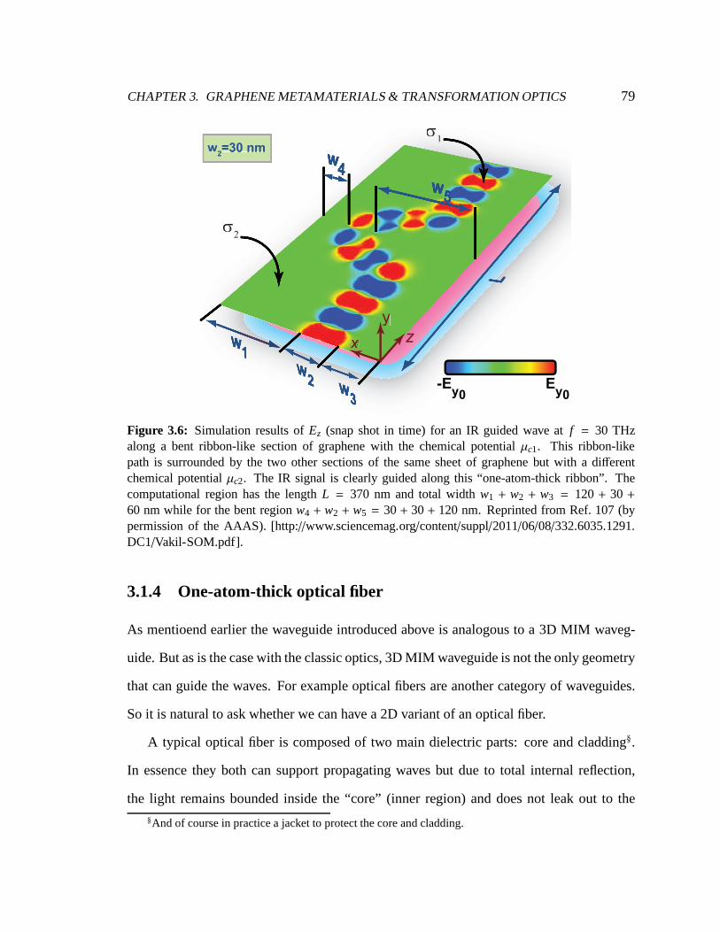
CHAPTER 3. GRAPHENE METAMATERIALS & TRANSFORMATION OPTICS 79
w2=30 nm
2
1
x
y
w2=30 nm
2
1
x
y
z
-Ey0
Ey0
Figure 3.6: Simulation results ofEz (snap shot in time) for an IR guided wave atf = 30 THzalong a bent ribbon-like section of graphene with the chemical potentialµc1. This ribbon-likepath is surrounded by the two other sections of the same sheetof graphene but with a differentchemical potentialµc2. The IR signal is clearly guided along this “one-atom-thickribbon”. Thecomputational region has the lengthL = 370 nm and total widthw1 + w2 + w3 = 120+ 30 +60 nm while for the bent regionw4 + w2 + w5 = 30+ 30+ 120 nm. Reprinted from Ref. 107 (bypermission of the AAAS). [http://www.sciencemag.org/content/suppl/2011/06/08/332.6035.1291.DC1/Vakil-SOM.pdf].
3.1.4 One-atom-thick optical fiber
As mentioend earlier the waveguide introduced above is analogous to a 3D MIM waveg-
uide. But as is the case with the classic optics, 3D MIM waveguide is not the only geometry
that can guide the waves. For example optical fibers are another category of waveguides.
So it is natural to ask whether we can have a 2D variant of an optical fiber.
A typical optical fiber is composed of two main dielectric parts: core and cladding§.
In essence they both can support propagating waves but due tototal internal reflection,
the light remains bounded inside the “core” (inner region) and does not leak out to the
§And of course in practice a jacket to protect the core and cladding.

CHAPTER 3. GRAPHENE METAMATERIALS & TRANSFORMATION OPTICS 80
w2=200 nm
Vbias
-Ey0Ey0
z
y
x
Figure 3.7: Simulation results ofEz (snap shot in time) for an IR splitter. This scenario is Similarto the waveguide case in Fig. 3.3 but the ribbon-like sectionsplits into two paths (L1 = 1077 nm,L2 = 560 nm,w = w1+w2+w3 = 600+ 200+ 600 nm). The graphene conductivity parameters aresimilar to those in Fig. 3.3. Reprinted from Ref. 106 (by permission of the AAAS). [http://www.sciencemag.org/content/332/6035/1291].
“cladding” (outer region). We propose a 2D analog of opticalfiber in Fig. 3.8.
Figure 3.8 shows full-wave simulation of 2D variant of optical fiber based on graphene.
Similar to an optical fiber, which has a high-index medium as THE core and a lower-index
medium as the cladding, one can create regions of conductivities such that the middle
segment has index larger than the side regions (by index we mean βSPP
k0; we will come back
to this definition in chapter 4. The simulation results indeed indicate that this geometry
guides the SPP mode through the middle region with minimal leakage of the energy to the
side regions. One caveat is that similar to an optical fiber the waveguide is not robust to
bends and too much bending can result in leakage of the signalto the side regions. But
on the positive side, since here the edge mode waves do not exist the amount of loss is
limited to that of the mode in the middle, resulting in possibly lower losses for the signal

CHAPTER 3. GRAPHENE METAMATERIALS & TRANSFORMATION OPTICS 81
-Ey0
Ey0
1
1
2
L
w1
w2
w2
Figure 3.8: Simulation results ofEz (snap shot in time) for an IR guided wave atf = 30 THz alonga ribbon-like section of graphene with the chemical potential µc2 = 150 meV. This ribbon-like pathis surrounded by the two other sections of the same sheet of graphene, but with a different chemicalpotentialµc,1 = 300 meV. Both of these chemical potentials result in positive imaginary part ofconductivity, but different values for effective SPP indexµc2 = 150 meV results in higher effectiveindex for the “core” region (similar to a 3D fiber for which core has higher SPP index for light). Inthis simulation, the IR signal is clearly seen to be guided along this “one-atom-thick ribbon”. Thecomputational region has the lengthL = 1 µmand total widthw2+w1 +w2 = 150+ 200+ 150 nm.Reprinted from Ref. 107 (by permission of the AAAS). [http://www.sciencemag.org/content/suppl/2011/06/08/332.6035.1291.DC1/Vakil-SOM.pdf].
transmission.
It is worth mentioning that these examples and scenarios areonly a few of myriad
possibilities that may follow from tailorability and tunability of graphene conductivity.
For instance Sounas & Caloz [99] have studied the surface plasmon polartions along a
magnetically biased graphene strip. They find that placing aPEC strip along one edge of
the graphene strip results in a non-reciprocity in the system, suggesting that wavenumbers
are not the same in opposite directions. A non-reciprocal phase shifter is suggested based
on this phenomenon. Another interesting prospect for this non-reciprocity in the system is
to have a category of waveguides known as one-way-waveguides. In nanophotonics it is
always a challenge to suppress back-reflection¶, which is result of superposition of forward
¶Interestingly this problem dates back to the days when engineers were searching for solutions to sup-press reflection from an antenna back into a transmission lines.

CHAPTER 3. GRAPHENE METAMATERIALS & TRANSFORMATION OPTICS 82
waves and reflected backward waves. In particular back-reflection could be parasitic for
optical signal processing applications that are based on slow-light systems [119]. Having
non-reciprocity in the system can be a solution to this problem. As we just mentioned
the characteristics of waves are different in opposite direction for the setup proposed by
Sounas & Caloz. But what if we operate in a range of frequency,where the forward mode
is propagating and the backward is below cutoff? This will result in suppression of the
backward wave, preveting formation of back-reflection. This will be a subject of future
study on graphene.
As another scenario of waveguiding Christensen et. al [16] propose a linear chain of
graphene nanodisks (withℑσg > 0) as a waveguide for SPP surface waves. This is indeed
2D analog of a waveguide made up of a linear chain of metallic nanoparticles [3, 11, 87].
The authors also investigate hybridization of plasmon modes in a pair of neighboring
aligned nanoribbon waveguides and the propagation characteristics as function of distance
of two ribbons. Tuning the distance of two waveguides could be a mechanism for control-
ling the dispersion of the mode (in some instances this distance can change the dispersion
relation of the modes dramatically). Authors’ suggest thattheir proposal can be a platform
for low-power optical signal detection.
Having the capability to guide SPPs across graphene, we may think of designing res-
onant cavities based on graphene waveguides. In the next section we will look at these
category of optical elements.
3.2 One-atom-thick cavities
Electrical engineers tend to describe any resonance phenomena using parallel or series
circuits of lumped elements (resistor, inductor and capacitor). But why?

CHAPTER 3. GRAPHENE METAMATERIALS & TRANSFORMATION OPTICS 83
This tendency exist because the concept of circuit and associating different behaviors
to circuit elements (i.e., dissipative behavior to resistors and reactive behavior to capaci-
tors and inductors) offers a more insightful way of analyzing physical phenomena. As just
mentioned to exploit the analogy, the resonance may not necessarily be originating from
interaction of actual lumped circuit elements. For instance in microwave engineering, or-
dinary lumped elements connected through wires do not function as efficient resonators,
and to build resonators, engineers resort to structural elements such as waveguides; by en-
closing waveguide ends and creating a closed structure thatdoes not radiate, with proper
design of geometry, a resonator can be constructed. Howevercircuit theory concepts are
still employed in analysis of resonant structures.
Here, as well, we take a similar approach. We design resonantcavities following theo-
retical concepts developed in chapter 2, section 2.2.4 and then analyze them using circuit
theory (especially using the concept of impedance).
Let us start with a simple scenario as depicted in Fig. 3.9. Weknow that a graphene
layer whose imaginary part of conductivity is positive supports TM SPP surface waves.
However if the imaginary part is negative these TM waves do not exist. So terminating a
graphene layer withσg,i > 0, on both ends, with two layers withσg,i < 0, would bound
the mode to be inside the region sandwiched between two otherregions (with negative
imaginary parts). But to make the structure resonant at a certain frequency, the cavity
dimensions must be designed properly—for example in the 1D geometry of Fig. 3.9 the
length of the cavityℓ should be chosen such that the cavity becomes resonant. In the
following section some rules-of-thumbs are proposed for design of resonant cavities.

CHAPTER 3. GRAPHENE METAMATERIALS & TRANSFORMATION OPTICS 84
y
z
x
l
Figure 3.9: (Schematic) 1D one-atom-thick resonant cavity using graphene. The two outer regionshave a conductivity whose imaginary part is negative while the region sandwiched between the twohas positive imaginary part of conductivity, thus supporting the TM SPP waves. The structure isuniform in x direction (∂/∂x = 0). The question is “Given that the mode does not leak out to twoouter regions, can we choose lengthℓ such that the cavity becomes resonant?”
3.2.1 Design of one-atom-thick cavities
1D One-atom-thick resonant cavity
The geometry in Fig. 3.9 may remind us of familiar Fabry-Perot interferometer in classic
optics, which is typically made of two parallel mirrors withhigh reflectivity. This geometry,
as well, is formed of two parallel one-atom-thick regions that can reflect the TM SPP waves
considerably as their imaginary parts of conductivity is negative. Since the wave does not
enter into these side regions, it has to reflect back. Of course some part of its energy radiates
away at the edges, resulting in less than 100% reflection fromthe boundaries. However as
we will see, we can still achieve resonance with imperfect walls (as is the case with an
imperfect Fabry-Perot interferometer).
As we know for a cavity with PEC walls (Γ = −1, whereΓ is reflection from the walls),
the resonance condition is simplyℓ = nλ2 for n = 1, 2, ..., whereℓ is length of cavity and
λ is the wavelength of the guided mode in the medium between twomirrors. But what if
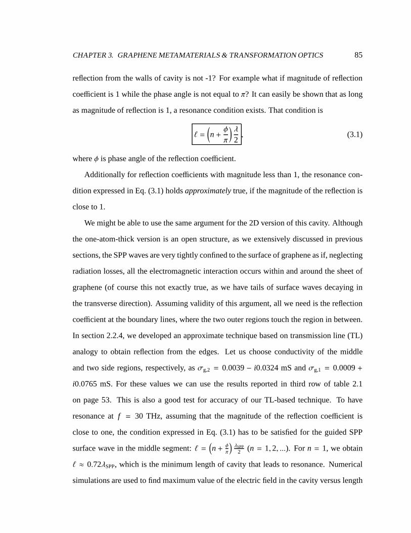
CHAPTER 3. GRAPHENE METAMATERIALS & TRANSFORMATION OPTICS 85
reflection from the walls of cavity is not -1? For example whatif magnitude of reflection
coefficient is 1 while the phase angle is not equal toπ? It can easily be shown that as long
as magnitude of reflection is 1, a resonance condition exists. That condition is
ℓ =
(
n+φ
π
)
λ
2, (3.1)
whereφ is phase angle of the reflection coefficient.
Additionally for reflection coefficients with magnitude less than 1, the resonance con-
dition expressed in Eq. (3.1) holdsapproximatelytrue, if the magnitude of the reflection is
close to 1.
We might be able to use the same argument for the 2D version of this cavity. Although
the one-atom-thick version is an open structure, as we extensively discussed in previous
sections, the SPP waves are very tightly confined to the surface of graphene as if, neglecting
radiation losses, all the electromagnetic interaction occurs within and around the sheet of
graphene (of course this not exactly true, as we have tails ofsurface waves decaying in
the transverse direction). Assuming validity of this argument, all we need is the reflection
coefficient at the boundary lines, where the two outer regions touch the region in between.
In section 2.2.4, we developed an approximate technique based on transmission line (TL)
analogy to obtain reflection from the edges. Let us choose conductivity of the middle
and two side regions, respectively, asσg,2 = 0.0039− i0.0324 mS andσg,1 = 0.0009+
i0.0765 mS. For these values we can use the results reported in third row of table 2.1
on page 53. This is also a good test for accuracy of our TL-based technique. To have
resonance atf = 30 THz, assuming that the magnitude of the reflection coefficient is
close to one, the condition expressed in Eq. (3.1) has to be satisfied for the guided SPP
surface wave in the middle segment:ℓ =(
n+ φπ
)
λSPP2 (n = 1, 2, ...). For n = 1, we obtain
ℓ ≈ 0.72λSPP, which is the minimum length of cavity that leads to resonance. Numerical
simulations are used to find maximum value of the electric field in the cavity versus length

CHAPTER 3. GRAPHENE METAMATERIALS & TRANSFORMATION OPTICS 86
Em
ax (
Norm
aliz
ed)
[a.u
.]
/ SPP
0.63 0.68 0.73 0.78 0.83
0
0.2
0.4
0.6
0.8
1
0
0.2
0.4
0.6
0.8
1
28 29 30 31 32
Em
ax (
Norm
aliz
ed)
[a.u
.]
0
0.2
0.4
0.6
0.8
1
0
0.2
0.4
0.6
0.8
1
A B
f (THz)
Lorentzian +t
Figure 3.10: A Maximum of magnitude of the electric field atf = 30 THz versus length of cavity(normalized toλSPPof 30 THz SPP).B Maximum of magnitude of the electric field versus frequencyof operation forℓ = 0.72λSPP, whereλSPP is the wavelength of guided SPP atf = 30 THz. Also aLorentzian lineshape is fitted to data–based on the fit the resonance frequency is 30.18 THz whilethe Lorentzian half-width is∼ 0.37 THz.
of cavity (see Fig. 3.10,A). The maximum peak is plotted against length, while keeping
frequency and the magnitude of the source fixed to examine ourproposed rule-of-thumb
ℓ =(
n+ φπ
)
λSPP2 . Ideally we would like to see the largest maximum peak of the electric field
for ℓ = 0.72λSPP, whereλSPP is the wavelength of guided SPP atf = 30 THz. There is a
relatively small discrepancy (less than 2% relative error)between the length predicted by
the Eq. (3.1) and the length for which resonance occurs at 30 THz. Although it is subtle,
this discrepency might be due to the fact that the magnitude of the reflection coefficient
is not exactly 1. Obviously the final goal is to design the cavity so that it resonates at
a desired frequency. Figure 3.10,B shows the absolute value of the maximum electric
field in the cavity versus frequency (the frequency dependence of conductivity of graphene
is accounted for by using Kubo formula). As can be seen for length ℓ = 0.72λSPP, the
resonance occurs at aroundf = 30.2 THz, resulting in less than 1% relative error. A
Lorentzian curve δ/π
( f− f0)2+δ2has been fitted to the numerical data. The fitting parameter are

CHAPTER 3. GRAPHENE METAMATERIALS & TRANSFORMATION OPTICS 87
0.72 SPP
10-2 1[a.u]
z
x y
|E|!1
g,i > 0
!2
g,i < 0!2
g,i < 0
Figure 3.11: Density plot of the magnitude of electric field vector onx-z plane forℓ = 0.72λSPPatf = 30.2 THz (whereλSPPis the wavelength of guided SPP atf = 30 THz).
Lorentzian half-widthδ ≈ 0.37 THz and the resonance frequencyf0 ≈ 30.18 THz.
Additionally density plot of the magnitude of electric fieldvector onx-z plane is pre-
sented in Fig. 3.11 (we note that the structure is uniform iny-direction). As can be seen
the field is enhanced considerably and is tightly confined to the surface of graphene, while
bounded in the middle segment.
In summary, it appears that the simple rule-of-thumb proposed for 1D cavities works
reasonably well in predicting location of resonance and canbe used to find the approximate
resonance length for a desired frequency.
2D One-atom-thick resonant cavity
Now let us consider another scenario, where the region of graphene supporting SPP waves
(σg,i > 0) is completely surrounded by a region that does not supportSPP waves (σg,i <
0)—a 2D scenario. For example consider the circular cavity depicted in Fig. 3.12 (desired
resonance frequency is 30 THz and values of conductivity areas in the case of 1D cavity).

CHAPTER 3. GRAPHENE METAMATERIALS & TRANSFORMATION OPTICS 88
y
z
x
Figure 3.12: (Schematic) 2D one-atom-thick resonant cavity using graphene. The outer region hasa conductivity whose imaginary part is negative while the central region has positive imaginary partof conductivity, thus supporting TM SPP waves. Again the question is whether we can find theoptimal radius for which this 2D cavity becomes resonant at adesired frequency?
Again the goal is to choose the radius of the cavity so it becomes resonant at a certain fre-
quency. Due to high confinement of the modes, as was the case for the 1D cavity case, we
may assume all the electromagnetic interaction occurs within and in the immediate vicinity
of the graphene layer, so we might be able to follow the same steps as in the problem of an
infinitely long cylindrical cavity. Let us start by writing the transverse component of the
electric field in the cavity as
Ez = A(kρ)[
E+z,0H(1)0 (kρρ) + E−z,0H
(2)0 (kρρ)
]
, (3.2)
where terme−pz is dropped since we are very close to the plane of graphene‖. In Eq. (3.2)
E+z,0 andE−z,0 are electric field amplitudes of the outgoing and incoming radial waves, and
A(kρ) is a function ofkρ (determined by boundary condition – see details in section 2.2.3;
here for our purpose knowledge of this term is not of concern.The boundary condition at
ρ = ρ0 can be written asE−z,0H
(2)0 (kρρ)
E+z,0H(1)0 (kρρ)
= Γ(ρ = ρ0), (3.3)
‖p =√
k2ρ − k2
0, as defined in section 2.2, wherekρ is the radial wavenumber; due to the geometry of the
problem, cylindrical coordinate system is chosen.

CHAPTER 3. GRAPHENE METAMATERIALS & TRANSFORMATION OPTICS 89
whereΓ(ρ = ρ0) is the reflection coefficient atρ = ρ0 boundary. Substituting Eq. (3.3) in
Eq. (3.2) and removing singularity at origin (which is due tosingularity of Hankel functions
at origin), the radiusρ0 has to satisfy following condition
H(2)0 (kρρ0)
H(1)0 (kρρ0)
= Γ(ρ = ρ0), (3.4)
which can be rewritten as
J0(kρρ0) − iY0(kρρ0)
J0(kρρ0) + iY0(kρρ0)= Γ(ρ = ρ0). (3.5)
For Γ(ρ = ρ0) = −1, Eq. (3.5) simplifies to the faimilar formJ0(kρρ0) = 0 (this is a well
known resonance condition for an infinitely long dielectriccylinder with PEC wall). Let
us for a moment assume thatkρ is real-valued. If so, the right-hand-side (RHS) of Eq. (3.5)
has magnitude 1, implying that that as long as the magnitude of reflection from the outer
region is 1, the condition expressed in Eqs. (3.4) and (3.5) can be simplified as
φ = −2 tan−1 Y0(kρρ0)
J0(kρρ0), (3.6)
whereφ is the phase angle of reflection coefficientΓ(ρ = ρ0). This condition still holds
approximatelytrue for reflection coefficients, whose magnitude is close to 1 (imperfect
PEC walls). We again use the value obtained from transmission line technique forΓ(ρ = ρ0)
[table 2.1, page 53]. Using the phase angle calculated in table 2.1 in Eq. (3.6) yields
ρ0 = 0.52λSPPas one condition for resonance (this is of course only one solution of many
possible ones). Numerical simulations are used to find maximum value of the electric field
(magnitude) in the cavity versus length of the cavity (see Fig. 3.13,A).
We examine whether at 30 THz the largest maximum peak of electric field occurs for
ρ0 = 0.52λSPP (λSPP is the wavelength of guided SPP atf = 30 THz). Again there is a
relatively small discrepancy (less than 2% relative error)between the length predicted by
the Eq. (3.6) and the length for which actual resonance occurs at 30 THz. Figure 3.10,
CHAPTER 3. GRAPHENE METAMATERIALS & TRANSFORMATION OPTICS 90
28 29 30 31 32
Em
ax (
Norm
aliz
ed)
[a.u
.]
0
0.2
0.4
0.6
0.8
1
0
B
f (THz)
Lorentzian *t
Em
ax (
Norm
aliz
ed)
[a.u
.]
/ SPP
0.42 0.47 0.52 0.57 0.62
0
0.2
0.4
0.6
0.8
1
A
Figure 3.13: AMaximum of magnitude of the electric field atf = 30 THz versus length of cavity—normalized toλSPPof 30 THz SPP.B Maximum of magnitude of the electric field versus frequencyof operation forρ0 = 0.52λSPP, whereλSPP is the wavelenght of guided SPP atf = 30 THz. Alsoa Lotentzian lineshape is fitted to data–based on the fit the resonance frequency is 29.70 THz whilethe Lorentzian half-width is∼ 0.30 THz.
B shows the absolute value of the maximum electric field in the cavity versus frequency.
As can be seen for lengthρ0 = 0.52λSPP, the resonance occurs at aroundf = 29.7 THz,
resulting in roughly 1% relative error. Fitting Lorentzianform δ/π
( f− f0)2+δ2to numerical data
yields fitting parameters asδ ≈ 0.30 THz (Lorentzian half-width) andf0 ≈ 29.70 THz
(resonance frequency).
Figure 3.14,A, illustrates the magnitude of they-component of electric field onx-z
andx-y planes, while Fig. 3.14,B, shows the magnitude of total electric field on the same
planes, suggesting that the electric field is substantiallyenhanced.
3.2.2 Analysis of one-atom-thick cavities
Of particular interest is to investigate how the resonant cavities introduced in previous
sections, enhance the radiation characteristics of an emitter, e.g. atoms, molecules and
nanoparticles. Since 2D circular cavity introduced, provides more field confinement com-

CHAPTER 3. GRAPHENE METAMATERIALS & TRANSFORMATION OPTICS 91
0 0.67[a.u] 0 1[a.u]
|E||Ey|BA
x y
z
x y
z
Figure 3.14: A andB Density plot of the magnitude of electric field vector and itsy-component onx-z and andx-y planes forρ = 0.52λSPPat f = 29.7 THz (whereλSPP is the wavelength of guidedSPP atf = 30 THz).
pared with the 1D geometry, here we focus our attention to theformer (2D case).
As mentioned in section 2.2.6,Purcell factorcaptures impact of the surrounding en-
vironment on spontaneous emission of an emitter (see discussion of Purcell factor on
page 63). In this study the emitter is described as a dipole oflength L oriented along
z-direction. The dipole carries currentI = 1 A and is located at distanceh ∼ 70 nm above
the cavity. To begin our analysis, we simplify Eq. (2.60) as following
Fp = 1+6πǫ0ω
Lk30
ℜEs,z(r0), (3.7)
in which Es,z is thez component of the scattered field due to the presence of the cavity.
Es,z can easily be obtained from numerical simulations by subtracting the incident field due
to the dipole from total field (we assumed a dipole of length 1 nm in our simulations to
mimic an infinitesimal dipole—deeply subwavelength). By evaluating the scattered field at
the location of the dipole, we obtain a Purcell factor of as large as approximately 8.2× 10⁴
for the dipole above the 2D cavity. We note that in this scenario the dipole is located at
approximately 70 nm above the cavity. Moving the dipole closer to the graphene sheet can
substantially enhance the Purcell effect∗∗. Our findings indicate that for a dipole sitting on∗∗The effect of distance from graphene is studied extensively in Ref.43

CHAPTER 3. GRAPHENE METAMATERIALS & TRANSFORMATION OPTICS 92
the graphene layer, in principle, one might achieve Purcellfactors as high as 107, consistent
with Ref. 54. These values are compared with the lower valuesfor Purcell factors of order
105 for the 1D cavity.
As we mentioned in section 3.2, to better understand the characteristics of the graphene
cavity, we can exploit a circuit analogy. However, the challenge is to describe the cavity
using combination of circuit elements such as resistor, inductor and capacitor. Greffet et.
al provide such a framework in Ref. 35. Let us briefly discuss their framework and then
apply it to our problem.
As we know the time averaged power radiated by a dipole (located atr0) into the elec-
tromagnetic field is [see Eq. (2.61)]
P0 =12ℜiωp · E∗(r0) (3.8)
Interestingly the structure of this equation is similar to the familiar form of electrical power
P = 12ℜIV∗ dissipated in a loadZL with resistanceR. Moreover, the electric field is given
by E(r0) =↔G(r0, r0;ω) · p(r0), which can be recast as follows [35]
E(r0) =
↔G(r0, r0;ω)−iω
· [−iωp(r0)]
. (3.9)
This equation also has a familiar structure and is similar tothe linear relation between
voltage and currentV = ZI in the circuit theory. Comparing Eqs. (3.8) and (3.9) with their
electrical counterparts and considering that the dipole only hasz component (p = pzz),
Greffet et. al have introduced following identifications [35]
I ↔ −iωpz(r0) V ↔ −Ez(r0) Z↔ −iGzz(r0, r0, ω)ω
, (3.10)
which enable us to establish the concept of complex impedanceZ = R+iY for a dipole (e.g.,
a quantum emitter). The real part of such impedance accountsfor loss (both radiative and
dissipative) and is simply expressed asℑGzz/ω. Additionally according to our discussion

CHAPTER 3. GRAPHENE METAMATERIALS & TRANSFORMATION OPTICS 93
in section 2.2.6, the spontaneous emission rate (decay rate) is proportional to the imaginary
part of Green’s function. As discussed in Ref. 35, this similarity constitutes a connection
between the decay rate and the resistive part of the impedance just defined (γ ∝ R). Such a
connection may provide an insightful way to analyze the cavity under study. For example
one can easily re-derive the Purcell factor using the concept of impedance by evaluating
the ratio between the resistance of the impedance of the dipole in vicinity of the cavityR
to that of the dipole in free-spaceR0 (Fp =RR0
).
The concept of impedance always finds significance when dealing with a collection of
interconnected elements. So the question is whether it is possible to define impedance for
other elements than the dipole. As introduced in Ref. 35, thesame concepts introduced can
also be applied to the cavity geometry, meaning that if the modes of the cavity are known,
it is also possible to define an impedance for the cavity basedon the Green’s function of
the cavity.
To obtain an expression for the impedance of the cavity, one can expand the Green’s
tensor in terms of orthonormal modes of the cavityun (∫
Vun · u∗mdr3 = δnm, whereδnm is
Kronecker delta) [35]
↔G(r , r ′;ω) =
∑
n
ω2
ǫ0
un(r ) ⊗ u∗n(r′)
ω2n
(
1− iQ
)
− ω2, (3.11)
where⊗ denotes the outer product,ωn is eigen-frequency associated with mode number
n andQ is the quality factor of the cavity. In Eq. (3.11),ω2n
(
1− iQ
)
is the complex fre-
quency accounting for the loss in the cavity. The elementlm of matrix representation of
equation (3.11) is obtained as
Glm(r , r ′;ω) =∑
n
ω2
ǫ0
un,l(r )u∗n,m(r ′)
ω2n
(
1− iQ
)
− ω2. (3.12)
Since the dipole is oriented inz-direction, as we just saw from Eq. (3.10), we are only
interested in evaluatingGzz. Assuming we are operating around the resonance frequency

CHAPTER 3. GRAPHENE METAMATERIALS & TRANSFORMATION OPTICS 94
ω0 (eigenfrequency), contribution from other modes are smalland we can write
Gzz(r M , r M;ω) =ω2
ǫ0
|uz(r M;ω0)|2
ω20
(
1− iQ
)
− ω2, (3.13)
in which rM is the point where the mode amplitude is maximum and sinceuz(r M;ω0) is a
normalized mode of the cavity (∫
V|un|2dr3 = 1), the effective mode volume for the cavity is
defined as [35]
Veff =1
|uz(r M;ω0)|2, (3.14)
which enables us to write Eq. (3.13) as following
Gzz(r M , r M;ω) =ω2
ǫ0
V−1eff
ω20
(
1− iQ
)
− ω2. (3.15)
Eqs. (3.10) and (3.15) suggest that the cavity can be regarded as a parallelRLC circuit
with R = Qωǫ0Veffω
20, L = 1
ǫ0Veffω20
andC = ǫ0Veff [35]. Finding the ratio ofR/R0 yields the
Purcell factor Fp =3Qλ3
4π2Veff[35]. Mode volumeVeff and quality factorQ can be obtained
from numerical simulations. Assuming losses are small, using perturbation method, one
can evaluateQ from half-power fractional bandwidth∆ ff0
of the resonator, where∆ f is the
distance between frequencies (aroundf0), for which the amplitude of the mode drops to1√2
of its maximum atf0 [86]
Q =f0∆ f. (3.16)
Using the results from numerical simulations and carrying the calculations through for
the 2D graphene cavity, we obtain quality factor of∼ 100 and effective mode volume of
1.6 × 10⁻²² m3 (1.6 × 10⁻⁷ · λ3 for λ = 10 µm), suggesting that the high Purcell factor is
mostly due to very small effective mode volume rather than high quality factor. In fact the
quality factor for the 2D cavity is in the same range as for the1D cavity (∼ 80), so the large
Purcell effect is mainly the result of the higher mode confinement in 2D case compared
with the 1D geometry.

CHAPTER 3. GRAPHENE METAMATERIALS & TRANSFORMATION OPTICS 95
Since in this section we were mostly concerned about analyzing the cavity characteris-
tics, we skip elaborating further on how the concept of impedance can be used to re-derive
the decay rate of the dipole in close proximity of the cavity.Greffet et. al offer an elegant
treatment of the problem in Ref. 35.
Lastly, on a totally different note, we would like to remark on the possibility of strong
coupling between the cavity and the emitter (dipole). In this regime the emitter might en-
able a strong plasmon-plasmon interaction, resulting inplasmon blockade, meaning that
for high intensity incident light, which results in strong coupling, average number of plas-
mons in the cavity do not follow a linear relationship with optical pump intensity (for
weak-coupling this relationship is linear regardless of power of optical pump) [65].
3.3 One-atom-thick reflectors
Pursuing our goal to establish graphene as a flatland platform for transformation optics
and metamaterials, here inspired by optical mirrors from classic optics, we introduce one-
atom-thick reflectors for infrared (IR) SPP surface waves based on graphene. We first
study the simple case of one-atom-thick straight line mirror and then show how a one-
atom-thick parabolic reflector (mirror) can be envisioned for focusing guided SPP waves
on the graphene [109].
3.3.1 One-atom-thick straight line mirror
Let us begin our theoretical study with a simple case: a straight line mirror which is one-
atom-thick variant of a plane mirror [109]—we coin term “line mirror” as opposed to plane
mirror since the thickness of graphene is extremely small compared to its other dimensions,
the boundary between two adjacent sections of a graphene layer is effectively a line rather

CHAPTER 3. GRAPHENE METAMATERIALS & TRANSFORMATION OPTICS 96
than a plane. By studying this relatively simple scenario wecan find a better understanding
of physics of more complicated reflectors based on graphene.As usual, the simulations are
at f = 30 THz for a free-standing graphene in air.
Earlier in this work we demonstrated that it is possible to tailor conductivity distribution
across graphene such that SPP surface waves reflect from a “boundary line” on a sheet of
graphene (section 2.2.4). And as we emphasized this phenomenon is the basic function
that many optical elements are built upon. For instance, a plane mirror in classic optics
creates an image of a point object behind the plane of mirror.For a plane mirror image is
formed at a point where if a straight line were drawn from thatpoint to the object, it would
make a right angle with, and is bisected by, the surface of themirror. However in a typical
mirror the image is 180 out of phase with the object and that is because the reflectionat
the surface of mirror is -1, meaning that the phase angle of reflection is 180. This phase
angle shows up as a phase difference between the object and image.
We would like to address the question that whether we can utilize the concept of image
mentioned above to describe the reflection from the boundary. Of course since the phase
of reflection coefficient is not the same as the perfect plane mirror, the phase difference
between image and object is not 180 anymore but the phase angle of reflection from the
boundary (incidentally this is the same as what reported in table 2.1 on page 53).
Figure 3.15,A, shows the simulation of the mirror scenario for the SPP surface wave
demonstrated on a one-atom-thick graphene layer. The conductivity values of the two
segments, calculated from the Kubo formula withT = 3 K andΓ = 0.43 meV, are, respec-
tively,σg,1 = 0.0009+ i0.0765 mS andσg,2 = 0.0039− i0.0324 mS. The front (closer) half
section withσg1,i > 0 supports a TM SPP, while the back (farther) half withσg2,i < 0 does
not. A TM SPP surface wave, with guided wavelength of about 144 nm, and with linear
phase front, is generated using superposition of three point sources, located atλSPP/16 from
the boundary (see Fig. 3.15,A). As we said in previous chapter, the reflection of SPP at

CHAPTER 3. GRAPHENE METAMATERIALS & TRANSFORMATION OPTICS 97
this line resembles the Fresnel reflection of a “plane” wave from a planar interface between
two media. Here, analogous reflection from a boundary line happens for the SPP across a
“one-atom-thick” platform. There is a little radiation loss due to high lateral confinement
of SPP surface wave.
To verify that the boundary line between the two segments acts as a “line” mirror,
we examine whether the modified version of image theory†† provides results similar to this
setting. We artificially add three “image” point sources (about 90 out of phase with respect
to the original sources and at the location of the images; 90 phase difference is dictated
by the phase angle of the reflection from the boundary line—obtained from table 2.1 on
page 53). The separation between “real” point sources and their “images” isλSPP/8 (twice
as distance between the object and mirror).
To conclude that two settings are equivalent, the superposition of the electric fields, in
the front segment, due to these two sets of sources – 3 “real” sources and 3 “image” sources
– should become similar to the original case. In Fig. 3.15,B, the simulation results display
the phase of they-component of the electric field in this scenario. The results demonstrate
equivalence between two cases (Fig. 3.15,A andB), suggesting that the boundary between
the two segments indeed mimics behavior of a mirror. We note that this mirror is not perfect
mirror as the magnitude of reflection from boundary line is not exactly 1, however as long
as the magnitude is close to 1, this modified image theory offers a good framework for
describing the physics of the problem.
Additionally, for the case where back region has large but positive imaginary part of
conductivity, similar results can be obtained (considering the phase angle of reflection
coefficient). In the following we study another example that illustrates this possibility.
Following our first proposal, one can now envisage several other scenarios.
††By modified version, we mean that in the classic image theory for a mirror the object and image are180 out of phase, while in our scenario this phase difference is the phase angle of the reflection from boundryline.

CHAPTER 3. GRAPHENE METAMATERIALS & TRANSFORMATION OPTICS 98
2, i < 0 1, i > 0
1, i > 0
z
xy
w
w
L2
L2
L1
L1
0 2!
BA
Figure 3.15: A Simulation results showing the phase ofz-component of the electric field for theSPP mirror scenario; the back (farther) region imaginary part of conductivity is negative and acts asan effective one-atom-thick straight line “mirror” reflecting anIR SPP guided wave generated fromthe 3 point sources located atλSPP/16 from the edge. The frequency of operation is assumed to bef = 30 THz.B the equivalent of the problem inA using image theory, where 6 points sources, i.e.,3 “real” point sources and 3 “image” sources have been considered with proper phase difference (L1
= 300 nm,L2 = 100 nm, andw = 200 nm). Distance between “real” sources and “image” sourcesis λSPP/8. From Ref. 109. Reprinted with permission from the Elsevier. [http://www.sciencedirect.com/science/article/pii/S0030401812001630].
Consider a 2-dimensional one-atom-thick version of a parabolic mirror for the SPP
on a single layer of graphene [109]. Figure 3.16 displays simulation results for such one-
atom-thick parabolic mirror, which may be created by patterning the graphene conductivity
nonuniformly. The conductivity values of the region in which the guided SPP surface wave
is launched (analog of air) and the opaque (mirror) region, at T = 3 K and with Γ =
0.43 meV, are, respectively,σg,1 = 0.0009+ i0.0765 mS andσg,2 = 0.00001+ i0.00174 mS.
Both sections haveσg,i > 0 supporting TM SPP surface wave, however the mirror-like
region has a conductivity with relatively large positive imaginary part, which results in
an SPP mode that is less confined than the other section. As a result we may observe
considerable amount of reflection of SPP at the parabolic mirror line. By proper design
of the shape of the boundary (here for example a parabola), one can focus the incoming
guided SPP surface wave to a point (for example here in the focus of the parabola). Our

CHAPTER 3. GRAPHENE METAMATERIALS & TRANSFORMATION OPTICS 99
numerical simulation verifies this concept as shown in Fig. 3.16.
Figure 3.16: Simulation results showing the magnitude of tangential component of the electricfield for a one-atom-thick parabolic “mirror” for the SPP focusing an IR SPP guided wave. Thefrequency of operation is assumed to be atf = 30 THz. The structure is 700 nm long and 500 nmwide. From Ref. 109. Reprinted with permission from the Elsevier. [http://www.sciencedirect.com/science/article/pii/S0030401812001630].
In sum, the intuitive image theory discussed here might be useful in analysis and design
of graphene-based devices that function based on reflectionof SPP surface waves within
a sheet of graphene. Also different one-atom-thick mirrors can form building blocks of
larger reflective optics systems.
3.4 Transformation optics using graphene
To tame electromagnetic waves we use materials with different optical properties to con-
trol and route the corresponding electric or magnetic fields(e.g. optical waveguides, lenses,
etc.). For example a bi-convex lens has a refractive index greater than that of air, resulting
in refraction of light waves, which due to curved shape of thelens will converge to a point.
However, relying only on homogeneous materials as buildingblocks to produce optical ele-
ments is endowed with fundamental limitations in functionality of these elements. It might

CHAPTER 3. GRAPHENE METAMATERIALS & TRANSFORMATION OPTICS 100
be difficult to overcome such limitation by merely relying on homogeneous materials—
e.g., beating diffraction limit in a conventional lens. To overcome these limitations we
may exploit and design optically inhomogeneous materials.Access to metamaterials and
design flexibility that they offer, enable engineering composite structures that might alle-
viate shortcomings inherent with conventional homogeneous refractive optics. But how
can we structure materials to exhibit a desired response? Transformation optics is one
solution [83].
Transformation optics (TO) offers recipes to design inhomogeneous materials to direct
the electromagnetic waves at will, overcoming limitationsof homogeneous optics. Trans-
formation optics deals with design of material properties on a subwavelength scale. From
fabrication point of view, although likely achievable, manufacturing materials with such
miniature inhomogeneities could be burdensome.
Earlier we mentioned graphenelocal conductivity can be tuned through different meth-
ods, e.g., uneven ground plane underneath the substrate holding graphene layer, with a
fixed dc voltage applied between the ground plane and the graphene sheet. This proposal
can result in a less complicated manufacturing mechanism, as it facilitates the fabrication
by transforming the process of creating subwavelength inhomogeneities to simply pattern-
ing the ground plane unevenly—which in turn results in the desired conductivity pattern.
In this section, by studying two theoretical examples and without going through the techni-
cal details of transformation optics, we demonstrate that graphene can be utilized as a new
platform for TO.
3.4.1 Luneburg lens with graphene
In our first example we study 2D variant of a Luneburg lens, i.e., one-atom-thick Luneburg
lens. The Luneburg lens is a spherical lens, whose refractive index gradually decreases in

CHAPTER 3. GRAPHENE METAMATERIALS & TRANSFORMATION OPTICS 101
radial direction from the center toward the surface (see theleft panel in Fig. 3.17, in which
the darker regions indicate higher refractive index). Due to gradient refractive index, locus
of focal points of this special lens lies on the surface of sphere. The Luneburg lens is
aberration-free and can focus light from all directions equally well. It is well known that
SPP
Si+
Figure 3.17: (Schematic) Top-left panel illustrates the concept of a spherical Luneburg lens, whiletop-right panel shows the 2D variant of this concept using graphene. Can we create a nonuniformprofile for conductivity across graphene (bottom panel) that results in the same function as in 3Dcase?
for a spherical Lunebrug lens in a background medium with refractive indexnbg the graded
refractive index should follow the relation
n(r) = nbg
√
2−( rR
)2
, (3.17)
whereR is th radius of the lens. As can be seen from Eq. (3.17), forr = R, n = nbg and for
r = 0, n =√
2nbg.

CHAPTER 3. GRAPHENE METAMATERIALS & TRANSFORMATION OPTICS 102
Our goal here is to design conductivity profile of a circular region within graphene layer
to function as a Luneburg lens for surface plasmons. In this context we define an effective
index for TM surface plasmon-polariton surface waves and try to find an equivalent form
for Eq. (3.17). Let us definenSPP=βSPP
k0. Then according to Eq. (2.13) we have
nSPP=
√
1−(
2σgη0
)2
, (3.18)
which can approximately be written as
nSPP≈2σg,iη0
, (3.19)
Substituting Eq. (3.19) in Eq. (3.17), we obtain a simplifiedform as
σg,i(r) ≈ σoutg,i
[
2−( rR
)2]− 1
2
, (3.20)
whereσoutg,i is the conductivity of the background graphene, within which the Luneburg
lens is created. Additionally to perform our numerical simulations, we consider a dis-
cretized Luneburg lens, composed of concentric rings with graded conductivities. Dis-
cretizing Eq. (3.20) results
σg,i[m] = σoutg,i
[
2−( rm+ rm−1
D
)2]− 1
2
, (3.21)
wheremcorresponds to the number of each ring, withm= 0 denoting the center of lens. In
our numerical simulation we used 10 segments with graded SPPindex following Eq. (3.21).
We also definer[m] = mr[1], wherer[1] = 75 nm. The corresponding chemical potential
and imaginary part of conductivity for each segment are reported in table 3.1. Numerical
simulations of this free-standing flat Luneburg lens is shown in Fig. 3.18, revealing that the
SPP generated from a “point-like” source is evolved into a “collimated beam” of SPP on
the graphene, as a conventional 3D Luneburg lens collimateswavefronts generated from a
point source into a 3D beam. The diameter of the lens is about 1.5µm, which is 0.15λ0—a

CHAPTER 3. GRAPHENE METAMATERIALS & TRANSFORMATION OPTICS 103
Table 3.1: Corresponding chemical potential and imaginary part of conductivity for each segmentof 2D Luneburg lens.
m Chemical potential (µc in meV) σg,i[m] in mS
1 221.0 0.12642 222.0 0.12713 224.0 0.12844 226.7 0.13045 231.1 0.13336 232.7 0.13727 244.0 0.14238 255.0 0.14909 268.5 0.158110 287.0 0.1706
notably subwavelength size. This study suggests that various subwavelength IR devices
(e.g., convex and concave lenses) might be possible using graphene.
Transformation optics offers an approach to control the propagation of light byspa-
tially varying the optical properties of a material [57, 83, 94]. Because the effective index
of the lens is changed gradually rather than abruptly, scattering losses can be reduced. In
addition to their imaging functionalities, lenses of any kind are basic elements for optical
signal processing (e.g., Fourier transforming). Thus, Luneburg lens based on graphene
could find applications in realizing optical signal processing elements such as spatial fil-
ters, correlators, and convolvers that are only one-atom-thick [106]. Another advantage of
Luneburg lens is the flexibility in control of its focal length that is vital to optical signal
processing applications. Lastly, this flat Luneburg lens has prospects for integration with
other photonic components.
As a second scenario for transformation optics using graphene, we look at 2D variant of
Pendry’s super lens proposed in 2000 [81]. The resolution offered by a conventional lens is
dictated by wave optics; no conventional lens can recover object features smaller than half
of wavelength of the light emanated from an object onto the surface of the lens. This lim-

CHAPTER 3. GRAPHENE METAMATERIALS & TRANSFORMATION OPTICS 104
0 2
D
L
w
Figure 3.18: One-atom-thick Luneburg lens: Simulation results showingthe phase ofEz of the SPPat f = 30 THz along the graphene (D = 1.5 µm, w = 75 nm,L = 1.6 µm). Reprinted from Ref. 106(by permission of the AAAS). [http://www.sciencemag.org/content/332/6035/1291].
2d dd
n = -1
object
plane
Image
plane
Figure 3.19: Schematic of a superlens;the red lines illustrate tails of the evanes-cent waves amplified by the slab.
itation of the conventional lens is associated with loss of high spatial Fourier components
(choosing axis of the lens asy, these spatial frequency components arekx andkz) of the
object as they become evanescent and die out before reachingsurface of the lens (meaning
that for(
k2x + k2
z
)1/2> ωc−1 the wave number inz direction becomes imaginary). Conse-
quently the resolution is limited to∼ πcω−1 = λ/2 [81]. Pendry’s proposal foils this limit,

CHAPTER 3. GRAPHENE METAMATERIALS & TRANSFORMATION OPTICS 105
thanks to features of DNG media. Assuming a slab of negative refractive index material,
these missing components can be recovered, if one conditionis satisfied:n = −1. If this
condition holds even the evanescent waves have total transmission through the slab. Also it
can be shown in the electrostatic limitc0
(
k2x + k2
z
)1/2 ≫ ω a slab of material withǫr = −1,
can still act as a superlens for TM-polarized waves radiatedfrom an object placed at dis-
tanced from a slab, which is 2d-thick (the image will be recovered at distanced behind the
slab) – see Fig. 3.19. Here we leverage this idea to create a 2Dsuperlens using graphene
as we can achieve negative and positive effective permittivity for graphene by changing
density of local carriers (effective permittivity was introduced based on conductivity in
section 2.2). Although originally superlens idea was not introduced in a transformation
optical context, later, transformation optics was employed to interpret the perfect lensing
mechanism [56]. As such here we study this case as an example of TO.
To begin consider a similar geometry as in Fig. 3.19 within graphene—i.e., a one-atom-
thick strip of width 2d and a point source at distanced in front of the strip. The boundary
line between the strip and background is virtual; as usual the strip is not necessarily a dis-
integrated segment from rest of the graphene layer. The contrast in conductivity of the strip
and its background can be achieved by proper choice of biases, resulting in required con-
ductivity values. With proper adjustment of the width of thestrip and separation between
the source and the strip, we can implement an approximate superlensing effect. Simulation
results forEz of SPP surface waves are presented in Fig. 3.20,A andB (for f = 30 THz).
PanelA shows simulation result for only one point source (the blackarea in the curve on
right displays normalized magnitude of transverse electric field for the point object). As
can be seen the proposed superlens yields a shaper image at distanced = 10 nm behind the
lens – compare red (with superlens) with blue (without superlens). However the real test
is to check whether this lens can capture two features of the object that have separation of
less than wavelength. To test this we consider a second scenario presented in Fig. 3.20,B.

CHAPTER 3. GRAPHENE METAMATERIALS & TRANSFORMATION OPTICS 106
Here two point sources are placed on the object line (which is10 nm in front of the lens).
The separation between these two objects iss = 55 nm – at 30 THz the wavelength of
guided SPP waves is about 144 nm, so 55 nm is less thanλSPP/2. It is worth mentioning
2dd d
i < 0 Strip
i < 0 Strip
100
50
0
50
100
0
0.2 0.4 0.6 0.8 1
With StripWithout Strip
|Ez|
|Ez,m
|
|Ez|
|Ez,m
|
2dd d
1-1 [a.u.] 1-1 [a.u.]
s
100
50
0
50
100
0
0.2 0.4 0.6 0.8 1
With StripWithout Strip
x
z y
x
z y
x (n
m)
x (n
m)
A B
s = 5
5 n
m
Figure 3.20: Flatland “superlens”: Simulation results forEz of SPP atf = 30 THz on the graphenewith a subwavelength strip region with conductivityσg,2 whose imaginary part is negative, whilethe rest of graphene has the conductivityσg,1 with positive imaginary part.A The object–a pointsource–and image lines are assumed to be, respectively, 10 nm away from the left and right edgesof the strip (w = 2d = 20 nm). The normalized intensity ofEz at the image line is shown for twocases with and without the strip (Normalization is with respect to their respective peak values). Thesubwavelength “focusing” is observable as the width of image with superlens is less than withoutsuperlens.B Now two sources, distanced apart by 55 nm, are placed in frontof the lens. Withoutsuperlens the image is blurry and the subwavelength features cannot be distinguished, whereasusing superlens high spatial frequencies associated with feature sizes less than wavelength can berecovered. Reprinted from Ref. 106 (by permission of the AAAS). [http://www.sciencemag.org/content/332/6035/1291].
that the superlensing can be linked to the existence of edge waves at the two edges of the
strip (these edge waves were introduced earlier). The perfect transmission of the evanes-
cent waves might be due to the excitation of two SPP edge wavesat the edges of the strip.
If two surface plasmons have similar energies, then they cancouple efficiently, resulting
in a resonance in the system and near perfect transmission. Of course in presence of loss,
which is the case here, the transmission cannot be perfect. As such the intensity of light

CHAPTER 3. GRAPHENE METAMATERIALS & TRANSFORMATION OPTICS 107
received on the image line is less than that of object.
The 2D superlens could serve as the basic building block for 2D hyperlens, finding ap-
plication in transforming deeply subwavelength “input’ field distributions to desired “out-
put” field distributions. This can be of use in optical signalprocessing and subwavelength
imaging within single layer of graphene. Following our workin Ref. 107, there have been
proposals for achieving hyperlens using graphene [6, 112].

108
Chapter 4
Fourier Optics on Graphene
Optical signal processing systems are designed to collect,process and transmit spatial in-
formation. For example optical filters perform mathematical operations (e.g., removing
some unwanted signal components or enhance others) on spatial signals, just as do electric
filters on time signals [33, 34]. One of the basic, yet integral, optical elements used in opti-
cal signal processing is the conventional lens. This element provides a simple yet powerful
way for obtaining Fourier transform of spatial signals. Optical signal processing based on
conventional lenses is not new. However, constructing miniaturized optical systems for
processing information at rates higher than the current state-of-the-art call for more than
conventional optics, requiring novel ideas in this realm. Here we propose graphene as a
new platform for “one-atom-thick” optical signal processing. Our theoretical findings show
that by creating a specific pattern of conductivity within a sheet of graphene, one can take
spatial Fourier transform of optical signals propagating as SPP waves. There are two ad-
vantages in using graphene as far as dimension is concerned:first, by using graphene, one
can shrink the thickness of the optical system down to multiples of a carbon atom diameter
(∼ 0.34 nm); second, since the optical signals propagate along the graphene in the form

CHAPTER 4. FOURIER OPTICS ON GRAPHENE 109
of tightly-confined SPP surface waves with guided wavelength much shorter than the free-
space wavelength other two dimensions of the system are alsosubstantially compressed to
deep subwavelength scales. These two features can facilitate realization of ultra-compact
optical systems. Additionally we previously mentioned that, at least in mid-IR region of
the spectrum, quality of SPPs in graphene might be better than in noble metals.
4.1 Lensing mechanism on graphene
The physical process underpinning operation of our proposed one-atom-thick lens is simply
borrowed from conventional optics; function of a conventional optical lens in transform-
ing light waves is replicated within graphene. When light isilluminated onto surface of
a conventional lens (e.g., when a plane wave is impinging on surface of the lens), far-
ther away from axis of the lens—which has higher refractive index compared with outside
medium—phase fronts experience smaller phase differences. The nonuniform phase differ-
ence distribution generates curved phase fronts at the output of the lens, coming into a focus
point. The same can be visualized for the SPP surface waves within graphene. Consider
the geometry depicted in the left panel of Fig. 4.1. This picture illustrates one of the pro-
posed methods to create nonuniform conductivity: using “uneven ground plane” to create
a lentil-shaped inhomogeneity in conductivity of a graphene sheet. In this method, highly
doped silicon substrate with uneven height profile may serveas the ground plane. Apply-
ing a fixed electric bias between the ground plane and graphene results in different values
of electric field at different segments of graphene due to differing distance between the flat
graphene and the uneven ground plane. This in turn may lead toan inhomogeneous carrier
density and consequently inhomogeneous chemical potential distribution, which produces
a nonuniform conductivity pattern across graphene layer. We note that to make numerical

CHAPTER 4. FOURIER OPTICS ON GRAPHENE 110
nSPP,2
!!nSPP,1 SPP
Vbias
"2
"1
Figure 4.1: Left: Sketch of proposed one-atom-thick lensing system foroptical Fourier trans-forming; geometry consists of a free-standing layer of graphene with inhomogeneous conductivitypattern across. Such inhomogeneity may be achieved by several techniques [106], e.g., by placinga highly doped silicon substrate with uneven height profile as ground plane underneath graphene.Left panel reproduced from Ref. 108 by permission of the American Physical Society. [http://prb.aps.org/abstract/PRB/v85/i7/e075434]. Right: Sketch of a planar gradient index lens similar to theone proposed in Ref. 116.
simulations simpler, we assume that the boundary line between the neighboring regions
with different conductivity values is “sharp”. In practice, the variation from one region
to another is not sharp; however, this will not affect validity of concepts introduced here.
Moreover, in practice the distance between the ground planeand graphene is filled with a
regular dielectric spacer, e.g. SiO2. Again for simplicity in our numerical simulations, we
assume that graphene is free standing and no spacer or groundplane is present.
In the following we show that this lentil-shaped region withdifferent conductivity (and
therefore different equivalent SPP refractive index) acts as a one-atom-thick lens. The
shape of the inhomogeneity is similar to cross section of a conventional optical double-
convex lens, but given flexibility in tuning graphene conductivity, other shapes can be
considered as well. For example a planar gradient index lenscan act similar to our proposed
lens [116] (Fig. 4.1, right panel).
Fourier transform of an object located at the front focal plane of a conventional double-
convex lens is formed at the back focal plane of the lens. Through numerical simulations,

CHAPTER 4. FOURIER OPTICS ON GRAPHENE 111
we show that the proposed inhomogeneity within graphene also obtains the Fourier trans-
form of objects located at its front focal line. To show this the following conditions must
hold:
(i) The lens must obtain the Fourier transform of a point-like object—which generates
circular phase fronts of the SPP on the graphene—placed at its front focal point as
linear phase fronts at exit
F t(x) = δ(x)∣
∣
∣
∣
fx=kx2π
= 1 , (4.1)
whereF andt(x) denote, respectively, the spatial Fourier transform and transmittance
of the object located at the front focal point, andfx andkx are spatial frequency and
wavenumber, respectively.
(ii) The lens must also obtain the Fourier transform of a uniform object—which generates
uniform linear phase fronts—placed at the front focal line,as circular phase fronts
converging at back focal point of the lens
F t(x) = 1∣
∣
∣
∣
fx=kx2π
= δ(kx
2π) (4.2)
(iii) The lens output must stay invariant, except for a linear phase shift, with respect to
shift in the input in the transverse direction; in other words, moving the object along
the front focal line must result only in a linear phase variation in the spatial frequency
domain at the back focal line. That is
F t(x) = δ(x− x0)∣
∣
∣
∣
fx=kx2π
= eikxx0 (4.3)
(iv) Finally the lens must yield the Fourier transform of an object with a uniform intensity
and a linear phase variation located at the front focal line as a converging circular
phase fronts to a point shifted along the back focal line
F t(x) = eik0x∣
∣
∣
∣
fx=kx2π
= δ(kx
2π− k0
2π) (4.4)

CHAPTER 4. FOURIER OPTICS ON GRAPHENE 112
Verifying conditions above, we can assure that the inhomogeneity on the graphene can
indeed perform as a lens.
In line with our intuition, our numerical simulations demonstrate that the inhomogene-
ity indeed exhibits these properties, confirming that the one-atom-thick lens obtains the
Fourier transform of the object at its focal line—since everything here occurs on a mono-
layer, the 2-dimensional object plane of regular optics collapses to a line, hence the de-
scriptor focal “line” [108].
As usual in our simulations, the temperature and the frequency of operation areT =
3 K and f = 30 THz, respectively. We emphasize that we could choose any other
temperature—e.g., room temperature—in these simulationsand still expect similar qual-
itative effects. The advantage of operating atT = 3 K, however, is that at this temper-
ature the amount of loss in graphene will be much less than thecorresponding amount
at room temperature. We would like to maintain the chemical potential of the “back-
ground” graphene layer atµc = 150 meV, corresponding to complex conductivityσg,1 =
0.0009+ i0.07651 mS. As mentioned in section 2.2.1, for this conductivity, the guided TM
SPP hasℜβSPP,1 = 69.34k0 andℑβSPP,1 = 0.71k0—equivalently effective SPP index is
nSPP= 69.34.
As a side note, to create a segment with desired shape and specific conductivity within
graphene, the chemical potential must be changed across that segment—for example to
create a region that acts as a double-convex one-atom-thicklens, a higher effective index
for the SPP surface waves is required. In order for the lens region to have an index larger
than the background graphene region (nSPP,1< nSPP,2), the ground plane can be patterned
such that its distance to the graphene sheet underneath the lens segment (d2) is larger than
its distance to the graphene beneath the background region (d1). For example, creating a
chemical potentialµc = 120 meV in the lens region, results in complex conductivityσg,2 =
0.0007+ i0.05271 mS. For this conductivity,ℜ(βSPP,1) = 100.61k0 andℑ(βSPP,1) = 0.64k0

CHAPTER 4. FOURIER OPTICS ON GRAPHENE 113
1
-1
[a.u.]
0
2
A
B
C
D
f
ff
f
w
LlensL
Figure 4.2: Simulation results for Fourier transforming within graphene for the case of point sourceillumination: A Top view of the snap shot in time of transverse component of the electric field ofguided SPP wave. The circular waves generated from the pointsource hit the one-atom-thick lensand exit as an SPP “line” wave.B Phase pattern of this SPP wave: this picture demonstrates the“point” to “line” Fourier transformation inA. C Top view of the snap shot in time of transversecomponent of the electric field of the SPP wave for caseA, where the point source is shifted alongthe left focal line.D Phase pattern of the SPP wave in partC, showing how the shift in the positionof the point source in the left focal line results in the phaseshift in the SPP line wave in the exitat the right focal line. Reproduced from Ref. 108 by permission of the American Physical Society.[http://prb.aps.org/abstract/PRB/v85/i7/e075434].
(equivalentlynSPP = 100.61). The dimensions for geometries in simulations of Figs. 4.2
and 4.3 are as following:L= 13.3λSPP,1≈ 1.916µm, Llens= 2.7λSPP,1= 4λSPP,2≈ 386.8 nm,
andw = 10λSPP,1 ≈ 1.444 µm. Figure 4.2 shows the simulation results for the case in
which circular SPP waves generated from a point source, guided along the graphene and
impinging onto the double convex lens. Figure 4.2,A andB, demonstrates the snap shot in
time and distribution of the phase of the transverse component of the electric field across

CHAPTER 4. FOURIER OPTICS ON GRAPHENE 114
the graphene layer. These results clearly demonstrate thatthe output of the proposed lens
is almost a linear SPP wave at the exit of the lens. So the condition (i) is satisfied. By post
processing the simulation results, we estimate the focal length of the proposed lens to be
around f = 4λSPP,1≈ 580.2 nm. Figure 4.2,C andD, shows the snap shot in time and
phase patterns of the transverse component of the electric field for the case in which the
location of point source is shifted down 2λSPP,1on the object line. It is clear that the effect
of shift appears as a linear phase shift in the spatial frequency domain—on the back focal
line. This confirms that condition (iii) holds.
Now we consider the scenario in which the lens is illuminatedwith a guided SPP sur-
face wave with a linear phase front (see Fig. 4.3). The lens transforms such SPP “line”
waves into converging circular SPP waves. Figure 4.3,A andB, displays the snap shot in
time and phase pattern of the transverse component of the electric field across the graphene
sheet. We can observe that at the output of lens, circular SPPwaves converge at the focal
point of the lens. This is a verification of condition (ii). InFig. 4.3,C andD, we present the
snap shot in time and distribution of the phase of the transverse component of the electric
field for the case of oblique incidence. The effect of shift appears as linear phase shift on
the image line as the focus moves along the back focal line, asserting that condition (iv)
mentioned above holds.
4.2 One-atom-thick 4f system
As an application for the lensing property, in the followingwe demonstrate a simple exam-
ple that is analog of an archetypal setup from conventional Fourier optics: a 4f system [34].
A 4f system consists of two identical lenses that are 2f apart from each other. This element,
which is four focal lengths long, recovers a replica of an object, with even transmittance

CHAPTER 4. FOURIER OPTICS ON GRAPHENE 115
0
2
w
Llens
L
f
ff
f
A
B
C
D
1
-1
[a.u.]
Figure 4.3: Simulation results for the same graphene lens, but for the incident guided SPP “line”wave:A Top view of the snap shot in time of transverse component of the electric field of the guidedSPP line wave incident on the lens from left, forming an SPP circular wave converging into the focalpoint on the right.B Phase pattern of this SPP wave inA. C Top view of the snap shot in time oftransverse component of the electric field of guided SPP “line” wave oblique incidence.D Phasepattern of this guided SPP wave inC. This demonstrates the “line” to “point” Fourier transformationand how the phase shift in the SPP line wave on the left can translate into the shift in the locationof the focal point on the right. Reproduced from Ref. 108 by permission of the American PhysicalSociety. [http://prb.aps.org/abstract/PRB/v85/i7/e075434].

CHAPTER 4. FOURIER OPTICS ON GRAPHENE 116
0 2
f f
f
2f
f 2f
Llens 1-1 [a.u.]
A
B
Figure 4.4: A 4f System on graphene:A Top view of the snap shot in time of transverse componentof the electric field for an SPP “line” wave incidence on the system from left.B Phase pattern ofthis guided SPP wave propagating through the 4f system, clearly showing how this one-atom-thick4f system transforms the SPP wave from “line” to “point”, andthen to “line” again. Reproducedfrom Ref. 108 by permission of the American Physical Society. [http://prb.aps.org/abstract/PRB/v85/i7/e075434].

CHAPTER 4. FOURIER OPTICS ON GRAPHENE 117
function of space, placed at one focal length in front of the first lens, at one focal length
behind the second lens. This follows from familiar identityF F t(x) = t−x. The first
lens yields the Fourier transform of the object at its back focal line. In turn, the second lens
performs another Fourier transform, delivering a duplicate of the object. In Fig. 4.4, the
simulation results are presented for a one-atom-thick “4f optical system”. The first lens is
illuminated with SPP waves with linear phase front. As can beseen, the illuminated waves
are approximately recovered at the exit of the second lens.
The 4f system is of particular significance for optical signal processing purposes, since
it forms foundation of a “4f correlator”, which finds application in implementing the math-
ematical operations of cross-correlation and convolution[49, 110]. As such a 4f correlator
enables a wide variety of image processing operations such as spatial filtering of optical
signals [33, 34]. A 4f system is also the basis for functions such as matched filtering and
phase-only matched filtering, that are employed in pattern recognition.
In summary our theoretical findings indicate that graphene can be a low-loss platform
for Fourier optics functions. Due to tight confinement of theguided SPP wave to the
surface of graphene, the entire signal processing occurs effectively in an extremely thin
volume around the graphene. As a result, one can envision several parallel graphene sheets
closely packed (but far enough apart not to affect the conductivity dispersion of each single
sheet) to have parallel and independent optical signal processing. This unique platform
could open new vistas in nanoscale and photonic circuitry and massively parallel platforms
for high-speed information processing [108].

118
Chapter 5
Conclusion
5.1 Summary
In this thesis we theoretically and numerically examined prospect of graphene, a mono-
layer of carbon atoms, as a new platform for one-atom-thick metamaterial and transfor-
mation optical devices. Owing to its unusual band structure, graphene exhibits properties
unlike that of any conventional material. Although graphene offers various exciting elec-
tronic features (which facilitates study of many condensed-matter physics concepts using
only a table-top experiment that may not have been possible otherwise), our interest in this
work was mainly focused on interaction of electromagnetic waves with this one-atom-thick
material and possible applications that could follow in optical and plasmonic design.
In chapter 2, we presented theoretical background underpinning the proposals in chap-
ters 3 and 4. In chapter 2 we first reviewed a theoretical model(Kubo formalism) for
graphene conductivity, which was used in our numerical simulations throughout this work.
As we mentioned, the results from this formula are in good agreement with experiments
by other groups, ensuring validity of physical concepts anddiscussions presented. The

CHAPTER 5. CONCLUSION 119
graphene conductivity is generally a complex quantity and accounts for loss and stored
energy in graphene (see the discussion in appendix A). This quantity depends on chemi-
cal potential (which is related to carrier concentration ingraphene), temperature, frequency
and scattering rate (which represents loss). We also observed that the conductivity is related
to two transition mechanisms: interband and intraband. Theintraband contribution takes
a familiar Drude form (free electron gas model) and is dominant below critical frequency
~ω = 2µc. Below this critical frequency losses are small, making frequencies lower than
this critical value favorable for design of mid-IR metamaterial devices based on graphene.
Since CO2 lasers are available in the range 28 THz to 32 THz, this range was chosen for
our studies. In this range of frequency, for temperatures around few Kelvins and for the
chemical potentials less than 300 meV losses are relativelysmall. For frequencies higher
than~ω = 2µc, the interband contribution becomes significant and since interband transi-
tions are lossy, these frequencies may not be favorable for realization of optical devices.
Then we showed that depending on the sign of imaginary part ofthe conductivity graphene
can support TE and TM surface waves. If imaginary part of the conductivity is positive,
graphene can support TM surface plasmon polariton (SPP) surface waves, while TE waves
are suppressed. Conversely if the imaginary part of conductivity is negative, the TM modes
are not present and instead TE waves are supported. As we studied in detail, TM modes
are tightly confined to the surface of graphene, showing potential for small-scale circuitry
(in other words they have very large guided wave numberβSPP,TM≫ k0). However the TE
modes have wave numbers comparable with that of the free-space (βSPP,TE∼ k0), making
them less attractive since they cannot be exploited in miniaturized circuits.
In chapter 3, we provided various examples and case studies,suggesting that graphene
can indeed be a superb platform for low-dimensional plasmonic metamaterial structures
and transformation optical devices. We showed that by creating inhomogeneous patterns
across graphene, we can reflect and refract TM SPP surface waves to direct these waves

CHAPTER 5. CONCLUSION 120
in desired forms. For example, we offered scenarios in which graphene could be used to
build waveguides or beam-splitters by simply varying conductivity nonuniformly across
the graphene layer. Several types of waveguides were proposed: a 2D variant of a metal-
insulator-metal waveguide, a 2D variant of a optical fiber waveguide and one-atom thick
waveguides based on coupling of edge modes. In general two different types of modes
could be identified. One set of modes are concentrated in the middle of the graphene,
while the other category, the so-called “edge modes”, are concentrated around the edges.
The edge modes happen to have smaller guided wavelength compared with the middle
region modes. Following the waveguiding scenarios presented, resonant cavities based on
graphene were studied. It was shown that using a 2D circular cavity one may achieve
Purcell factors as high as 107 (depending on the distance of the emitter from the cavity),
suggesting that graphene might also be an excellent medium for enhanced light-matter
interaction. It was noted that this high Purcell factor is largely due to the very small mode
volume of the cavity rather than very large quality factor ofthe cavity. Then we looked at
a category of devices based on graphene inspired by conventional mirrors in classic optics.
It was argued that a segment within graphene with negative imaginary part of conductivity
may act as a mirror for SPP waves. Modified version of conventional image theory was
exploited to describe reflection from such region of conductivity. Additionally, we showed
that the function of mirror might as well be mimicked by a region of conductivity whose
imaginary part is positive but large enough to enable total internal reflection of the TM
waves. Mirror is a fundamental element in classic optics andseveral devices are built
upon concept of mirror. Similar devices for SPP surface waves can be envisioned based on
graphene, although more compact thanks to atomically thin graphene.
Finally in chapter 4, we introduced the concept of one-atom-thick Fourier optics using
graphene. It was illustrated that by creating a region with different effective SPP index
(defined asβSPP
k0) that is shaped similar to cross section of a 3D lens, it is possible to achieve

CHAPTER 5. CONCLUSION 121
Fourier transforming functions on a single layer of graphene. As it is well known, an optical
lens is the building block of optical signal processing systems. This elements is the basis of
systems for filtering spatial signals. Our findings can pave the way for realizing high-speed
low-dimensional signal processing elements using graphene. In such paradigm, one may
envision stacks of graphene layers spaced by dielectric layers – that are only hundreds of
nanometer thick – to form a compact optical information processing system that is orders
of magnitude smaller than the current state-of-the-art.
5.2 Future directions
The field of graphene metamaterials and transformation optics is in its infancy. In this
thesis we talked about several examples of graphene-based metamaterials, however many
of these ideas might still be far from implementation and need further detailed studies.
Moreover, there are just various directions to pursue on thetopics we introduced in this
thesis; it is indeed impossible to summarize all of these directions here, but we refer to a
subset of them that could be followed in the future.
• Mid-infrared circuits using graphene: Interestingly, our first excitement about
graphene was whether it can serve as a new platform for optical nano-circuits in-
troduced in Refs. 23 and 25. Although we have had some progresses in this terri-
tory (see appendix D for some primary results), this idea is worth investigating and
developing further, as it can lead to a new class of circuits that are fast, light and
ultra-small.
• Fourier optics using graphene: As discussed in chapter 4, graphene is an excellent
host for Fourier optics. Although we have laid out the basicsand showed thw possi-
bility of Fourier optics functions on graphene, the idea is worth pursuing for further

CHAPTER 5. CONCLUSION 122
studies. Expanding ideas in chapter 4, one can achieve larger-scale information pro-
cessing systems in mid-IR domain that are much faster than the current available
systems.
• Efficient coupling of a plane wave to graphene SPPs: As pointed out in sec-
tion 2.2.7, it is of great significance to couple power efficiently to graphene SPPs.
Our studies showed that the common techniques in conventional plasmonics are not
effective for coupling light with SPP modes (the coupling efficiencies are below 1%).
However by proper design of layered nanostructure (such as aplasmonic-dielectric-
plasmonic layered nanosphere), one might be able to largelyincrease the coupling
efficiency. This could be subject of further investigation and studies.
• Inverse scattering problem on graphene and applications for tomography: An-
other interesting problem is the study of inverse scattering of SPP from inhomo-
geneities within graphene. In other words whether it would be possible to retrieve
the conductivity of an inhomogeneity by detecting the scattered SPP field due to
that entity. This problem particularly is of interest in tomography applications using
graphene (see Fig. 5.1). Tomography using graphene can become a powerful tech-
nique in imaging non-flat objects (consider an object with uneven height profile) for
which direct imaging is not an option, since it may cause damages to the object under
study. Additionally this technique is capable of detectingsubwavelength features of
non-flat objects.
5.3 Final Thoughts
Graphene is indeed intriguing; aside from its 2-dimensionality and low losses in mid-IR,
one feature that makes it particularly favorable, is its tunability and the design flexibility

CHAPTER 5. CONCLUSION 123
z
yx
B (x, y)
Detection Scattered field
Inverse Radon
Transform
(x, y)
h(x, y)
Figure 5.1: Left panel shows a future idea about how graphene may be used to recover the heightprofile of an unknown bump. On the right panel the steps required to retrieve the profile are illus-trated.
it offers. Since graphene’s first isolation, prospects for graphene electronics have been
extensively studied by condensed matter physicist and engineers. This work and several
others suggest that graphene is also an excellent candidatefor plasmonics and photonics.
Graphene can be the base material for a new generation of circuits that integrate electronics,
photonics and plasmonics functionalities.

Appendices
124

125
Appendix A
Analogy between Graphene ComplexConductivity and a Parallel RLC Circuit
Here we briefly point out an analogy between graphene complexconductivity model and
a parallel RLC circuit (see Fig. A.1). As we know the total admittance of a parallel RLC
circuit is written as
Y =1−iωL
− iωC +G
= G+ i
(
ωL − 1ωC
)
= G+ iB (A.1)
whereY, G andB respectively denote admittance, conductance (1R) and suceptance. Comparing
this equation with conductivity of grapheneσ = σr + iσi, we can draw a simple analogy:
the real part of conductivity represent loss of graphene (similar to conductance of the RLC
circuit), while the imaginary part of conductivity relatesto the stored energy in graphene
(asC andL store energy in different cycles and causing the reactive behavior of the circuit).
As a result we might interpret the collective reactive response of the electrons in graphene
based on the sign of imaginary part of conductivity. As we have discussed in the main text,

APPENDIX A. CIRCUIT ANALOGY FOR CONDUCTIVITY 126
L RC
Figure A.1: Analogy between parallel RLC circuit and complex conductivity of graphene.
graphene can attain both positive and negative values of imaginary part. However other
conventional 2-dimensional electron gas (2DEG) systems, e.g. GaAs/AlGaAs quantum-
well structures, conductivity can only have positive values. We have seen that graphene,
due to this feature, can support TE SPP waves, whereas other 2D electron systems do
not [67].

127
Appendix B
Methods for Numerical Simulations
As each simulation required a different treatment and special care, elaborating on subtle
details of all simulations in this work is not in the scope of this thesis and probably not in
the interest of the readers. As such below we provide the general method of simulations.
We have used commercially available full-wave electromagnetic simulator software,
CST Studio Suite™ to perform our numerical simulations [1]. For the purpose of3D sim-
ulations, the thickness of graphene is assumed to be 1 nm, although other extremely small
values for this thickness obtain similar results. This technique is based on the derivation
of dispersion relation in chapter 2. We assumed 1 nm thickness for graphene and as-
signed the corresponding permittivity in our simulations according to the derivation shown
in section 2.2. As long as the thickness chosen is extremely small compared to the wave-
length, the choice of thickness is not essential—for example assume thickness of 0.5 nm
for graphene and finding the corresponding permittivity value, yields almost exactly the
same simulation results.
Due to the large contrast in the dimensions of the graphene layer, i.e., contrast between
thickness and width and between thickness and length, and due to the special form of

APPENDIX B. METHODS FOR NUMERICAL SIMULATIONS 128
the conductivity function of graphene, time-domain methodis not appropriate (it usually
required a very long run-time and sometimes led to instability) and we chose frequency-
domain Finite Element Method (FEM) solver in the CST Studio Suite. This solver solves
the problem for a single frequency at a time. For each frequency sample, the system of lin-
ear equation is solved by an iterative solver. Adaptive tetrahedral meshing with a minimum
feature resolution of 0.5 nm was used in all simulations. A discrete port (a point source
which is equivalent of an infinitesimal dipole antenna) or waveguide ports were utilized for
the excitation of surface-Plasmon polariton (SPP) wave in the structures. All the simula-
tions reached proper convergence; a residual energy of 10−5 of the peak value was reached
in the computation region.
To absorb all the energy at the ends of the computational domain and to have approx-
imately zero-reflection boundary on the receiving sides, inall the simulations a technique
similar to the well known Salisbury Shield method [29] was implemented (with proper
modifications for a TM SPP mode).
Depending on the nature of the problem, perfect magnetic conducting (PMC), perfect
electric conducting (PEC) or open boundary conditions wereapplied to different bound-
aries, to mimic the two-dimensionality of the geometry.

129
Appendix C
Universal Plasmon Dispersion forGraphene Nanoribbon Waveguides
Christensen et. al [16] propose an interesting methodologyto find a universal dispersion re-
lation for graphene nanoribbons’ plasmon modes. In their study they argue that the plasmon
modes are of electrostatic nature (due to relatively small size of the waveguide compared
with the wavelength of light). As such the modes can be treated as 2D multi-poles. Elec-
trostatic is scale-invariant thus the wavelength does not define anabsolutelength scale. As
such the resonances of the nanoribbon system are determinedonly based on the geometry
and optical properties of graphene. By neglecting losses, denoting the width of nanoribbon
by W, for each mode, one can define scaling parameter
ζ =1
4πǫ0
ℑσ(ω)ωW
, (C.1)
which at resonance peak frequency is independent ofW, µc and other physical parame-
ters, and only depends on dimensionless quantityβ∞W. Then for each mode analytical
curves can be extracted (through curve-fitting) for the relation betweenζ andβ∞W. Such
analytical relations with Eq. C.1 can be used to determine the dispersion relation or cutoff
condition for SPP modes of graphene. From Eq. C.1 we can also find the width at which

APPENDIX C. DISPERSION OF GRAPHENE NANORIBBONS 130
the cutoff occurs
W =λSPP
4π2ζ, (C.2)
which is different from the familiar conditionλSPP for a classical rectangular waveguide.
For a detailed discussion of this topic please see [16].

131
Appendix D
Mid-Infrared nano-circuits usingGraphene
The concept of optical nanocircuits using subwavelength plasmonic and conventional di-
electric nanoparticles was first proposed by our group in 2005 [25]. Depending on the
real part of its permittivity, a nanoparticle can mimic behavior of lumped elements such
as inductor and capacitor; a plasmonic nanoparticle whose imaginary part of permittivity
is negative can act as an inductor while nanoparticles made up of conventional dielectric
(ℜǫ > 0) may behave as a capacitor. Additionally any particle withnon-zero imaginary
part of permittivity can act as a resistor. Field of metamaterial can assist us in realizing
desired material properties for these nanoparticles.
Here we propose graphene as a platform for integrated optical nanocircuits. As we
have seen throughout this thesis, graphene conductivity can be tuned locally using chem-
ical doping or/and dc electric bias. Also in section 2.2, we introduced an equivalent per-
mittivity based on graphene conductivity. Then we showed that the real part of such equiv-
alent permittivity is linked to the negative of the imaginary part of graphene conductivity
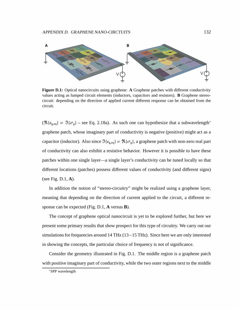
APPENDIX D. GRAPHENE NANO-CIRCTUITS 132
V V
A B
Figure D.1: Optical nanocircuits using graphene:A Graphene patches with different conductivityvalues acting as lumped circuit elements (inductors, capacitors and resistors).B Graphene stereo-circuit: depending on the direction of applied current different response can be obtained from thecircuit.
(ℜǫg,eq ∝ ℑσg – see Eq. 2.18a). As such one can hypothesize that a subwavelength∗
graphene patch, whose imaginary part of conductivity is negative (positive) might act as a
capacitor (inductor). Also sinceℑǫg,eq ∝ ℜσg, a graphene patch with non-zero real part
of conductivity can also exhibit a resistive behavior. However it is possible to have these
patches within one single layer—a single layer’s conductivity can be tuned locally so that
different locations (patches) possess different values of conductivity (and different signs)
(see Fig. D.1,A).
In addition the notion of “stereo-circuitry” might be realized using a graphene layer,
meaning that depending on the direction of current applied to the circuit, a different re-
sponse can be expected (Fig. D.1,A versusB).
The concept of graphene optical nanocircuit is yet to be explored further, but here we
present some primary results that show prospect for this type of circuitry. We carry out our
simulations for frequencies around 14 THz (13−15 THz). Since here we are only interested
in showing the concepts, the particular choice of frequencyis not of significance.
Consider the geometry illustrated in Fig. D.1. The middle region is a graphene patch
with positive imaginary part of conductivity, while the twoouter regions next to the middle
∗SPP wavelength

APPENDIX D. GRAPHENE NANO-CIRCTUITS 133
I
g,i
> 0
g,i
< 0
g,i
< 0
C C
Cf, CCf, C Cf, L
L
RLRC RC
B
A
Iac
Figure D.2: A series graphene nano-circuit:A The geometry of a series graphene nanocircuit; asshown in the bottom part the middle region behaves as an inductor while the two outer regionsto the middle region act as capacitors; the material losses of each segment is described as resistorℜσg , 0 (also a snapshot in time of the electric field vector is shown, indicating that the electricfield direction flips upon entering from one patch to another). B illustrates the circuit model of thesame geometry, however effect of fringe electric field are described as capacitance in parallel withthe original elements.
region have negative imaginary part of conductivity. The length of the middle region and
outer regions are, respectively, 69.2 nm and 15.4 nm—overall length of circuit is 100 nm,
which is much less than the SPP wavelength at 14 THz (∼ 775 nm), so the circuit can be
deemed as a lumped circuit. This circuit can be fed by two electrodes that are sketched
schematically in the figure (note that the structure is 2-dimensional in the lateral direction).
This geometry can be regarded as a series combination of two capacitors and one in-
ductor each shunt with a resistor as shown in Fig. D.1,A. Also Fig. D.1,B, shows a more
sophisticated circuit model for the geometry, describing the effect of fringe electric fields
by use of capacitors in parallel with each element.

APPENDIX D. GRAPHENE NANO-CIRCTUITS 134
The total impedance of the circuit is defined as following
Z =VI= −
∫
lE · dl
∮
SǫE · ds
, (D.1)
in which l is a line through the circuit andS is a mathematical surface cutting cross section
of the circuit†. The electric field can be obtained from full-wave numericalsimulations.
Using the results obtained from simulations, we can find the total impedance of the circuit
as a function of frequency (as shown in Fig. D.3). However to verify validity of the equiv-
alent circuit proposed, we have to evaluate the capacitance, inductance and resistance of
each lumped element of the equivalent circuit and examine whether the circuit combination
proposed yields a similar impedance as the simulations. Theadmittance of these segments
can be obtained using following expressions
YC =σg,C
WlC − iωCf,C, YL =
σg,L
WlL − iωCf,L, (D.2)
whereσg,C andσg,L denote the complex conductivity of the capacitive and inductive seg-
ments andW is the width of the circuit (w = 35 nm). The total impedance then is
Z =2
YC+
1YL. (D.3)
In Eq. D.2,Cf,L andCf,C are equivalent fringe capacitances that capture the effect of the
electric field fringe. To compute these fringe capacitances, we assumed that the fringe
fields can be associated to two cylindrical wires at two ends of each segment with diameter
D equal to the thickness of graphene (t). Based on this idea and the fact that the capacitance
of a two-wire transmission line follows the form
C f = πǫ0W
cosh−1(
lD
) , (D.4)
†This mathematical surface crosses the middle of that graphene sheet and is extended such that the fringefield lines cross this surface

APPENDIX D. GRAPHENE NANO-CIRCTUITS 135
0
20
40
60
80
100
120
|Zeq
| (K
)
!80
!40
0
40
80
13 13.5 14 14.5 15
f (THz)13 13.5 14 14.5 15
f (THz)
Arg
[Zeq
] (D
eg)
Full-wave simulation
CKT theory, with fringe
CKT theory, without fringe
Figure D.3: Series graphene circuit impedance based on numerical simulations and circuit theory.
we can compute the fringe capacitance parallel with each segment. Figure D.3 also shows
the impedance of the circuit based on the proposed circuit model (with and without the
fringe capacitances). As clearly can be seen the impedance based on the circuit model (with
fringe capacitances) mimics very closely the impedance obtained from the simulations
(using Eq. D.1).
In summary here we show-cased a graphene-based series circuit, which can be analyzed
using conventional circuit theory. Although this study is in its early stage, it may herald a
potential for integrated optical nanocircuits, thanks to tunability of graphene conductivity.
136
Appendix E
Matlab Code for Calculation of ComplexConductivity of Graphene
This is a piece of code written in Matlab that we used to calculate the complex conductivity
of graphene using Kubo Formula.
%%%%%%%%%%%%%%%%%%%%%%%%%%%%%%%%%%%%%%%%%%%%%%%%%%%%%%%%%%%%%%%%% %% Calculation of Conductivity of Graphene using Kubo Formul a %% Author: Ashkan Vakil %% %%%%%%%%%%%%%%%%%%%%%%%%%%%%%%%%%%%%%%%%%%%%%%%%%%%%%%%%%%%%%%%%%clcclear;
j = sqrt( −1);e = 1.6e −19;K B = 1.3806503e −23;T = 3;hb = (6.626e −34)/(2 * pi);% tau = 3e −12; % form GW Hanson paper% tau = .64e −12; % Soljacic paper% gamma = 1/(2* tau);gamma = 0.65460252158e12; % Gusynin J. Phys.: Cond. Mat.sigma min = 6.085e −5;vf = 10ˆ6;
w = pi * 2e12 * linspace(5,400,200); % CO2 lasers are this range

APPENDIX E. MATLAB CODE 137
m = length(w);mu c = 1.6e −19* [.15];n = length(mu c);mu ct = repmat(mu c,m,1); % generating the matrix for chemical potentialwt = repmat(transpose(w),1,n); % generating the matrix forfrequency
sigma d intra = ...−j * ((eˆ2 * K B* T)./(pi * hbˆ2 * (wt −j * 2* gamma))). * ((mu ct)/(K B* T) ...+2* log(exp( −mu ct/(K B* T))+1)); %intraband term
sigma d inter = zeros(m,n); % interband term variable definition
eps = 1.6e −19* linspace(0,10,600000);q = length(eps);
% Interband term calculationsfor i = 1:n
muc = mu c(i);f d meps = 1./(1+exp(( −eps−muc)/(K B* T)));f d peps = 1./(1+exp((eps −muc)/(K B* T)));for k = 1:m
sigma d inter(k,i) = ...trapz(eps, −(j * eˆ2 * (w(k) −j * 2* gamma)/(pi * hbˆ2)) ...
* (f d meps−f d peps)./((w(k) −j * 2* gamma)ˆ2 −4* (eps/hb).ˆ2));end
end
sigma tot = sigma d inter+sigma d intra; % total conductivityC = 'k' , 'r' , 'b' , 'c' , 'g' , 'm' , 'y' ;p1 = zeros(1,n);pp1 = zeros(1,n);s1 = cell(1, n);p2 = zeros(1,n);pp2 = zeros(1,n);s2 = cell(1, n);
%%%%%%%%%%%%%%%%%%%%%%%%%%%%%%%%%%%%%%%%%%%%%%%%%%%%%%%%%%%%%%%%%%%%%%%%%%%%%%%%%%%%%%%%%%%%%%%%%%%%%%%%%%%%%%%%%%%%%%%%%%%%%%%%%%%%%%%%%%%%%%%%figure(1)subplot(2,1,1)for i = 1:n
hold onp1(i) = ...
plot(1e −12* w/2/pi,(transpose(real((sigma d inter(:,i)))))/ ...(eˆ2/hb/4), 'Color' , C i , 'Linewidth' ,2);hold on
pp1(i) = ...plot(1e −12* w/2/pi,(transpose(real((sigma d intra(:,i)))))/ ...(eˆ2/hb/4), 'Color' , ...
Ci , 'Linewidth' ,2, 'Linestyle' , ' −.' );hold ons1 i = sprintf( 'mu c,%d = %d meV',i,1e3 * mu c(i)/(1.6e −19));
end

APPENDIX E. MATLAB CODE 138
ind = 1:n;% axis squarebox onxlabel( 'f (THZ)' , 'fontsize' ,20, 'fontweight' , 'b' );ylabel( 'Re( \sigma)' , 'fontsize' ,20, 'fontweight' , 'b' );legend(p1(ind), s1 ind );
%%%%%%%%%%%%%%%%%%%%%%%%%%%%%%%%%%%%%%%%%%%%%%%%%%%%%%%%%%%%%%%%%%%%%%%%%figure(2)
subplot(2,1,2)hold onfor i = 1:n
hold onp2(i) = ...
plot(1e −12* w/2/pi, −(transpose(imag((sigma d inter(:,i)))))/ ...(eˆ2/hb/4), 'Color' , C i , 'Linewidth' ,2);hold on
pp2(i) = ...plot(1e −12* w/2/pi, −(transpose(imag((sigma d intra(:,i)))))/ ...(eˆ2/hb/4), 'Color' , ...
Ci , 'Linewidth' ,2, 'Linestyle' , ' −.' );hold ons2 i = sprintf( 'mu c,%d = %d meV',i,1e3 * mu c(i)/(1.6e −19));
end% axis squarebox onxlabel( 'f (THZ)' , 'fontsize' ,20, 'fontweight' , 'b' );ylabel( 'Im( \sigma)' , 'fontsize' ,20, 'fontweight' , 'b' );% legend(p2(ind), s2 ind );

Bibliography
[1] CST Microwave Studio (from CST Studio Suite 2012). http://www.cst.com/.
[2] A. Alu and N. Engheta. Optical nanotransmission lines:synthesis of planar left-
handed metamaterials in the infrared and visible regimes.Journal of the Optical
Society of America B, 23(571), 2006.
[3] A. Alu and N. Engheta. Theory of linear chains of metamaterial/plasmonic particles
as subdiffraction optical nanotransmission lines.Physical Review B, 74(205436),
2006.
[4] A. Alu and N. Engheta. Three-dimensional nanotransmission lines at optical fre-
quencies: A recipe for broadband negative-refraction optical metamaterials.Physi-
cal Review B, 75(0243304), 2007.
[5] D. R. Anderson. Graphene-based long-wave infrared tm surface plasmon modulator.
Journal of Optical Society of America B, 27(818), 2010.
[6] A. Andryieuski and A. V. Lavrinenko. Graphene hyperlensfor terahertz radiation.
Physical Review B, 86(121108), 2012.
[7] C. A. Balanis.Advanced Engineering Electromagnetics. John Wiley & Sons, New
York, 1989.
139

BIBLIOGRAPHY 140
[8] Q. Bao and K. P. Loh. Graphene photonics, plasmonics, andbroadband optoelec-
tronic devices.ACS Nano, 6(5):3677–3694, 2012.
[9] Q. Bao, H. Zhang, B. Wang, Z. Ni, C. H. Y. X. Lim, Y. Wang, D. Y. Tang, and K. P.
Loh. Broadband graphene polarizer.Nature Photonics, 5:411–415, 2011.
[10] W. L. Barnes, A. Dereux, and T. W. Ebbesen. Surface plasmon subwavelength
optics.Nature, 424(824), 2003.
[11] M. L. Brongersma, J. W. Hartman, and H. A. Atwater. Electromagnetic energy trans-
fer and switching in nanoparticle chain arrays below the diffraction limit. Physical
Review B, 62(24), 2000.
[12] W. Cai and V. Shalaev.Optical Metamaterials: Fundamentals and Applications.
Springer, New York, 2010.
[13] V. V. Cheianov, V. Falko, and B. L. Altshuler. The focusing of electron flow and a
veselago lens in graphene p-n junctions.Science, 315(1252), 2007.
[14] J. Chen, M. Badioli, P. Alonso-Gonzalez, S. Thongrattanasiri, F. Huth, J. Osmond,
M. Spasenovic, A. Centeno, A. Pesquera, P. Godignon, A. Z. Elorza, N. Camara,
F. J. Garcıa de Abajo, R. Hillenbrand, and F. H. L. Koppens. Optical nano-imaging
of gate-tunable graphene plasmons.Nature, 487:77–81, 2012.
[15] P-Y. Chen and A. Alu. Atomically thin surface cloak using graphene monolayers.
ACS Nano, 5(7), 2011.
[16] J. Christensen, A. Manjavacas, S. Thongrattanasiri, F. H. L. Koppens, and
F. J. Garcıa de Abajo. Graphene plasmon waveguiding and hybridization in indi-
vidual and paired nanoribbons.ACS Nano, 6(1), 2011.

BIBLIOGRAPHY 141
[17] R. E. Collin. Foundations for Microwave Engineering. John Wiley & Sons, New
York, 2000.
[18] I. Crassee1, J. Levallois, A. L. Walter, M. Ostler, A. Bostwick, E. Rotenberg,
T. Seyller, D. van der Marel1, and A. B. Kuzmenko. Giant faraday rotation in single-
and multilayer graphene.Nature Physics, 7(1816), 2010.
[19] Jozsef Cserti, Andras Palyi, and Csaba Peterfalvi. Caustics due to a negative refrac-
tive index in circular graphene p-n junctions.Physical Review Letters, 99(246801),
2007.
[20] R. Dehbashi, D. Fathi, S. Mohajerzadeh, and B. Forouzandeh. Equivalent left-
handed/right-handed metamaterial’s circuit model for the massless dirac fermions
with negative refraction.IEEE Journal of Selected Topics in Quantum Electronics,
16(394), 2010.
[21] N. Engheta. Special issue on ‘wave interaction with chiral and complex media’.
Journal of Electromagnetic and Waves Applications, 6(5/6), 1992.
[22] N. Engheta. An idea for thin subwavelength cavity resonators using metamaterials
with negative permittivity and permeability.IEEE Antennas and Wireless Propaga-
tion Letters, 1(1), 2002.
[23] N. Engheta. Circuits with light at nanoscales: Opticalnanocircuits inspired by meta-
materials.Science, 317(5845), 2007.
[24] N. Engheta and G. V. Eleftheriades. Metamaterials: Fundamentals and applications
in the microwave and optical regimes.Proceedings of the IEEE, 99(10), 2011.

BIBLIOGRAPHY 142
[25] N. Engheta, A. Salandrino, and A. Alu. Circuit elements at optical frequen-
cies: nanoinductors, nanocapacitors, and nanoresistors.Physical Review Letters,
95(095504), 2005.
[26] N. Engheta and R. W. Ziolkowski.Metamaterials: Physics and Engineering Explo-
rations. IEEE-Wiley, New York, 2006.
[27] L. A. Falkovsky and S. S. Pershoguba. Optical far-infrared properties of a graphene
monolayer and multilayer.Physical Review B, 76(153410), 2007.
[28] L.A. Falkovsky and C. C. Persheguba. Optical far-infrared properties of a graphene
monolayer and multilayer.Physical Review B, 76(153410), 2007.
[29] R. L. Fante and M. T. McCormack. Reflection properties ofthe salisbury screen.
IEEE Transactions on Antennas and Propagation, 36(10), 1988.
[30] Z. Fei, G. O. Andreev, W. Bao, L. M. Zhang, A. S. McLeod, C.Wang, M. K. Stew-
art, Z. Zhao, G. Dominguez, M. Thiemens, M. M. Fogler, M. J. Tauber, A. H. Castro
Neto, C. N. Lau, F. Keilmann, and D. N. Basov. Infrared nanoscopy of dirac plas-
mons at the graphene sio2 interface.Nano Letters, 11:4701–4705, 2011.
[31] Z. Fei, A. S. Rodin, G. O. Andreev, W. Bao, A. S. McLeod, M.Wagner, L. M. Zhang,
Z. Zhao, M. Thiemens, G. Dominguez, M. M. Fogler, A. H. CastroNeto, C. N.
Lau, F. Keilmann, and D. N. Basov. Gate-tuning of graphene plasmons revealed by
infrared nano-imaging.Nature, 487:82–85, 2012.
[32] J. K. Gansel, M. Thiel, M. S. Rill, M. Decker, K. Bade, V. Saile, G. von Freymann,
S. Linden, and M Wegener. Gold helix photonic metamaterial as broadband circular
polarizer.Science, 325(5947), 2009.

BIBLIOGRAPHY 143
[33] J. D. Gaskill.Linear Systems, Fourier Transforms, and Optics. John Wiley & Sons,
1978.
[34] J. W. Goodman.Introduction to Fourier Optics. Roberts & Co. Publishers, Colorado,
2005.
[35] J-J. Greffet, M. Laroche, and F. Marquier. Impedance of a nanoantenna and a single
quantum emitter.Physical Review Letter, 105(117701), 2010.
[36] A. G. Grushin, B. Valenzuela, and M. A. H. Vozmediano. Effect of coulomb interac-
tions on the optical properties of doped graphene.Physical Review B, 80(155417),
2009.
[37] V. P. Gusynin and S. G. Sharapov. Transport of dirac quasiparticles in graphene:
Hall and optical conductivities.Physical Review B, 73(245411), 2006.
[38] V. P. Gusynin, S. G. Sharapov, and J. P. Carbotte. Unusual microwave response of
dirac quasiparticles in graphene.Physical Review Letters, 96(256802), 2006.
[39] V. P. Gusynin, S. G. Sharapov, and J. P. Carbotte. Magneto-optical conductivity in
graphene.Journal of Physics: Condensed Matter, 19(2), 2007.
[40] V. P. Gusynin, S. G. Sharapov, and J. P. Carbotte. Sum rules for the optical and hall
conductivity in graphene.Physical Review B, 75(165407), 2007.
[41] G. W. Hanson. Dyadic greens functions and guided surface waves for a surface
conductivity model of graphene.Journal of Applied Physics, 103(064302), 2008.
[42] G. W. Hanson. Dyadic greens functions for an anisotropic, non-local model of biased
graphene.IEEE Transactions on Antennas and Propagation, 56(3), 2008.

BIBLIOGRAPHY 144
[43] P. A. Hidorbro, A. Y. Nikitin, C. Gonzalez-Ballestero, L. Martın-Moreno, and F. J.
Garcıa-Vidal. Supperradiance mediated by graphene surface plasmons.Physical
Review B, 85(155438), 2012.
[44] P. A. Huidobro, M. L. Nesterov, L. Martın-Moreno, and F. J. Garcıa-Vidal. Trans-
formation optics for plasmonics.Nano Letters, 10(1985), 2010.
[45] E. H. Hwang and S. Das Sarma. Dielectric function, screening, and plasmons in
two-dimensional graphene.Physical Review B, 75(205418), 2007.
[46] A. Ishimaru. Electromagnetic Wave Propagation, Radiation, and Scattering. Pren-
tice Hall, New Jersey, 1991.
[47] M. Jablan, H. Buljan, and M. Soljacic. Plasmonics in graphene at infrared frequen-
cies.Physical Review Letters, 80(245435), 2009.
[48] Z. Jacob, L. V. Alekseyev, and E. Narimanov. Optical hyperlens: Far-field imaging
beyond the diffraction limit. Optics Express, 14(18), 2006.
[49] B. Javidi and J.L Horner. Optical pattern recognition for validation and security
verification.Optical Engineering, 33(6), 1994.
[50] L. Ju, B. Geng, J. Horng, C. Girit, M. Martin, Z. Hao, H. A.Bechtel, X. Liang,
A. Zettl, Y. R. Shen, and F. Wang. Graphene plasmonics for tunable terahertz meta-
materials.Nature Nanotechnology, 6:630634, 2011.
[51] J. S. Kilby. Invention of the integrated circuits.IEEE Transaction on Electron
Devices, 23(7), 1976.
[52] J. T Kim and S-Y Choi. Graphene-based plasmonic waveguides for photonic inte-
grated circuits.Optics Express, 19(24), 2011.

BIBLIOGRAPHY 145
[53] J-T Kim, J. Kim, H. Choi, C-G. Choi, and S-Y. Choi. Graphene-based photonic
devices for soft hybrid optoelectronic systems.Nanotechnology, 23(34), 2012.
[54] F. H. L. Koppens, D. E. Chang, and F. J. Garcıa de Abajo. Graphene plasmonics: A
platform for strong light-matter interactions.Nano Letter, 11(8), 2011.
[55] A. E. Leanhardt, T. A. Pasquini, M. Saba, A. Schirotzek,Y. Shin, D. Kielpinski,
D. E. Pritchard, and W. Ketterle. Cooling bose-einstein condensates below 500
picokelvin. Science, 301(5639):1513–1515, 2003.
[56] U. Leonhardt. General relativity in electrical engineering. New Journal of Physics,
8(247), 2006.
[57] U. Leonhardt. Optical conformal mapping.Science, 312(5781), 2006.
[58] Z. Q. Li, E. A. Henriksena, Z. Jiang, Z. Hao, M. C. Martin,P. Kim, H. L. Stormer,
and D. N. Basov. Dirac charge dynamics in graphene by infrared spectroscopy.
Nature Physics, 4(532), 2008.
[59] Z. Q. Li, E. A. Henriksena, Z. Jiang, Z. Hao, M. C. Martin,P. Kima, H. L.
Stormer, and D. N. Basov. Supplementary information for “dirac charge dynam-
ics in graphene by infrared spectroscopy”. http://www.nature.com/nphys/journal/
v4/n7/extref/nphys989-s1.pdf, 2008.
[60] M. Liu, X. Yin, E. Ulin-Avila, B. Geng, T. Zentgraf, L. Ju, F. Wang, and X. Zhang.
A graphene-based broadband optical modulator.Nature, 474:64–67, 2011.
[61] M. Liu, X. Yin, and X. Zhang. Double-layer graphene optical modulator. Nano
Letters, 12:1482–1485, 2012.

BIBLIOGRAPHY 146
[62] I. Llatsera, C. Kremersb, A. Cabellos-Aparicioa, J. M.Jornetc, E. Alarcona, and
D. N. Chigrin. Graphene-based nano-patch antenna for terahertz radiation.Photon-
ics and Nanostructures – Fundamentals and Applications, 10(4):353–358, 2012.
[63] S. A. Maier. Plasmonics: Fundamentals and Applications. Springer, Bath, United
Kingdom, 2007.
[64] K. F. Mak, M. Y. Sfeir, Y. Wu, C. H. Lui, J. A. Misewich, andT. F. Heinz. Measure-
ment of the optical conductivity of graphene.Physical Review Letters, 101(196405),
2008.
[65] A. Manjavacas, P. Nordlander, and F. J. Garcıa de Abajo. Plasmon blockade in
nanostructured.ACS Nano, 6(2):1724–1731, 2012.
[66] S. A. Mikhailov. Non-linear electromagnetic responseof graphene.Europhysics
Letters, 79(27002), 2007.
[67] S. A. Mikhailov and K. Ziegler. A new electromagnetic mode in graphene.Physical
Review Letters, 99(016803), 2007.
[68] S. A. Mikhailov and K. Ziegler. Nonlinear electromagnetic response of graphene:
frequency multiplication and the self-consistent-field effects. Journal of Physics:
Condensed Matter, 20(384204), 2008.
[69] E. G. Mishchenko, A. V. Shytov, and P. G. Silvestrov. Guided plasmon in graphene
p-n junction.Physical Review Letters, 104(156806), 2010.
[70] G. E. Moore. Cramming more components onto integrated circuits. Electronics,
38(8), 1965.

BIBLIOGRAPHY 147
[71] A. Y. Nikitin, F. Guinea, F. J. Garcıa-Vidal, and L. Martın-Moreno. Edge and waveg-
uide thz surface plasmon modes in graphene micro-ribbons.Physical Review B,
84(161407), 2011.
[72] A. Y. Nikitin, F. Guinea, F. J. Garcıa-Vidal, and L. Martın-Moreno. Fields radiated
by a nanoemitter in a graphene sheet.Physical Review B, 84(195446), 2011.
[73] A. Y. Nikitin, F. Guinea, F. J. Garcıa-Vidal, and L. Martın-Moreno. Surface plasmon
enhanced absorption and suppressed transmission in periodic arrays of graphene
ribbons.Physical Review B, 85(081405(R)), 2012.
[74] K. S. Novoselov and A. K. Geim. The rise of graphene.Nature Material, 6:183–191,
2007.
[75] K. S. Novoselov, A. K. Geim, S. V. Morozov, D. Jiang, M. I.Katsnelson, I. V.
Grigorieva, S. V. Dubonos, and A. A. Firsov. Two-dimensional gas of massless
dirac fermions in graphene.Nature, 438:197–200, 2005.
[76] K. S. Novoselov, A. K. Geim, S. V. Morozov, D. Jiang, Y. Zhang, S. V. Dubonos,
I. V. Grigorieva, and A. A. Firsov. Electric field effect in atomically thin carbon
films. Science, 306(5696), 2004.
[77] L. Novotny and B. Hetch.Principles of Nano-optics. Cambridge University Press,
New York, 2006.
[78] E. Ozbay. Plasmonics: merging photonics and electronics at nanoscale dimensions.
Science, 311(5758), 2006.
[79] E. D. Palik. Handbook of Optical Constants of Solids I. Academic Press, Orlando,
Florida, 1985.

BIBLIOGRAPHY 148
[80] N. Papasimakis, Z. Luo, Z. X. Shen, F. De Angelis, E. Di Fabrizio, A. E. Nikolaenko,
and N. I. Zheludev. Graphene in a photonic metamaterial.Optics Express, 18(8),
2010.
[81] J. B. Pendry. Negative refraction makes perfect lens.Physical Review Letters,
85(18), 2000.
[82] J. B. Pendry, A. Aubry, D. R. Smith, and S. A. Maier. Transformation optics and
subwavelength control of light.Science, 337(6094), 2012.
[83] J. B. Pendry, D. Schurig, and D. R. Smith. Controlling electromagnetic fields.Sci-
ence, 312(5781), 2006.
[84] J. B. Pendry and D. R. Smith. Reversing light with negative refraction. Physics
Today, 57(6), 2004.
[85] N. M. R. Peres, R. M. Ribeiro, and A. H. Castro-Neto. Excitonic effects in the optical
conductivity of gated graphene.Physical Review Letters, 105(055501), 2010.
[86] D. M. Pozar.Microwave Engineering. John Wiley & Sons, New Jersey, 2005. 3rd
edition.
[87] M. Quinten, A. Leitner, J. R. Krenn, and F. R. Aussenegg.Electromagnetic energy
transport via linear chains of silver nanoparticles.Optics Letters, 23(17), 1998.
[88] F. Rana. Graphene terahertz plasmon oscillators.IEEE Transaction on Nano-
Technology, 7(91), 2008.
[89] J. Rho, Z. Ye, Y. Xiong, X. Yin, Z. Liu, H. Choi, G. Bartal,and X. Zhang. Spher-
ical hyperlens for two-dimensional sub-diffractional imaging at visible frequencies.
Nature Communications, 1(143):450454, 2010.

BIBLIOGRAPHY 149
[90] R. G. Rojas. Wiener-hopf analysis of the em diffraction by an impedance discon-
tinuity in a planar surface and by an impedance half-plane.IEEE Transactions on
Antennas and Propagation, 36(1), 1988.
[91] N. Rotenberg, M. Spasenovic, T. L. Krijger, B. le Feber, F. J. Garcıa de Abajo, and
L. Kuipers. Plasmon scattering from single subwavelength holes. Physical Review
Letters, 108(127402), 2012.
[92] Z. Ruan and S. Fan. Superscattering of light from subwavelength nanostructures.
Physical Review Letter, 105(013901), 2010.
[93] A. Salandrino and N. Engheta. Far-field subdiffraction optical microscopy using
metamaterial crystals: Theory and simulations.Physical Review B, 74(075103),
2006.
[94] D. Schurig, J. J. Mock, B. J. Justice, S. A. Cummer, J. B. Pendry, A. F. Starr, and
D. R. Smith. Metamaterial electromagnetic cloak at microwave frequencies.Sci-
ence, 314(5801), 2006.
[95] B. Sensale-Rodriguez, R. Yan, M. M. Kelly, T. Fang, K. Tahy, W. S. Hwang, D. Jena,
L. Liu, and H. G. Xing. Broadband graphene terahertz modulators enabled by intra-
band transitions.Nature Communications, 3(780), 2012.
[96] R. A. Shelby, D. R. Smith, and S. Schultz. Experimental verification of a negative
index of refraction. IEEE Antennas and Wireless Propagation Letters, 292(5514),
2001.
[97] A. Sihvola. Metamaterials in electromagnetics.Metamaterials, 1(1), 2007.
[98] A. Sommerfeld. Partial Differential Equations in Physics. Academic Press Inc.,
New York, 1949. chapter 6: Problems of Radio (English version).

BIBLIOGRAPHY 150
[99] D. L. Sounas and C. Caloz. Edge surface modes in magnetically biased chemically
doped graphene strips.Applied Physics Letters, 99(231902), 2011.
[100] D. L. Sounas and C. Caloz. Electromagnetic nonreciprocity and gyrotropy of
graphene.Applied Physics Letters, 99(021911), 2011.
[101] P. Tassin, T. Koschny, M. Kafesaki, and C. M. Soukoulis. A comparison of graphene,
superconductors and metals as conductors for metamaterials and plasmonics.Nature
Photonics, 6:259264, 2012.
[102] T. N. Theis and P. M. Solomon. It’s time to reinvent the transistor! Science,
327(5973), 2010.
[103] S. Thongrattanasiri, F. H. L. Koppens, and F. J. Garcıa de Abajo. Complete
optical absorption in periodically patterned graphene.Physical Review Letters,
108(047401), 2012.
[104] S. Thongrattanasiri, A. Manjavacas, and F. J. Garcıade Abajo. Quantum finite-size
effects in graphene plasmons.ACS Nano, 6(2), 2012.
[105] S. Thongrattanasiri, Ivan Silveiro, and F. J. Garcıa de Abajo. Plasmons in electro-
statically doped graphene.Applied Physics Letters, 100(201105), 2012.
[106] A. Vakil and N. Engheta. Transformation optics using graphene. Science,
332(6035):1291–1294, 2011.
[107] A. Vakil and N. Engheta. Transformation optics using graphene: Supporting online
material. http://www.sciencemag.org/content/332/6035/1291/suppl/DC1, 2011.
[108] A. Vakil and N. Engheta. Fourier optics on graphene.Physical Review B,
85(075434), 2012.

BIBLIOGRAPHY 151
[109] A. Vakil and N. Engheta. One-atom-thick reflectors forsurface plasmon polariton
surface waves on graphene.Optics Communications, 285(16), 2012.
[110] A. VanderLugt.Optical Signal Processing. Wiley, New York, 1993.
[111] V. G. Veselago. The electrodynamics of substances with simultaneously negative
values ofǫ andµ. Soviet Physics Uspekhi, 10(509), 1968.
[112] J. Wang, Y. Xu, H. Chen, and B. Zhang. Ultraviolet dielectric hyperlens with layered
graphene and boron nitride.Journal of Materials Chemistry, 31(22), 2012.
[113] T. O. Wehling, K. S. Novoselov, S. V. Morozov, E. E. Vdovin, M. I. Katsnelson,
A. K. Geim, and A. I. Lichtenstein. Molecular doping of graphene. Nano Letters,
8(1):173–177, 2008.
[114] P. R. West, S. Ichii, G. V. Naik, N. K. Emani, V. M. Shalaev, and A. Boltasseva.
Searching for better plasmonic materials.Laser& Photonics Reviews, 4(6), 2010.
[115] A. R. Wright, X. G. Xu, J. C. Cao, and C. Zhang. Strong nonlinear optical response
of graphene in the terahertz regime.Applied Physics Letters, 95(072101), 2000.
[116] H. J. Xu, W. B. Lu, Y. Jiang, and Z. G. Dong. Beam-scanning planar lens based on
graphene.Applied Physics Letters, 100(051903), 2012.
[117] H. Yan, X. Li, B. Chandra, G. Tulevski, Y. Wu, M. Freitag, W. Zhu, P. Avouris, and
F. Xia. Tunable infrared plasmonic devices using graphene/insulator stacks.Nature
Nanotechnology, 7:330–334, 2012.
[118] X. Yang, J. Yao, J. Rho, X. Yin, and X. Zhang. Experimental realization of three-
dimensional indefinite cavities at the nanoscale with anomalous scaling laws.Nature
Photonics, 6:450454, 2012.

BIBLIOGRAPHY 152
[119] Z. Yu, G. Veronis, Z. Wang, and S. Fan. One-way electromagnetic waveguide
formed at the interface between a plasmonic metal under a static magnetic field
and a photonic crystal.Physical Review Letter, 100(023902), 2008.
[120] W. Zhou, J. Lee, J. Nanda, S. T. Pantelides, S. J. Pennycook, and J-C. Idrobo. Atom-
ically localized plasmon enhancement in monolayer graphene. Nature Nanotechnol-
ogy, 7:161–165, 2012.