Transceiver Front-End Technology for Software Radio ... · Transceiver Front-End Technology for...
29
Transceiver Front-End Technology for Software Radio Implementation of Wideband Satellite Communication Systems Fred Daneshgaran * , Massimiliano Laddomada † Keywords Software Radio, Reconfigurable Payload, Transceiver Front-end, Wideband Receiver, Satellite Communication 1. Introduction The term Software Radio (SR) is used to encompass a wide range of agile, multimode, programmable radio systems that can operate over a wide frequency band, and be able to “speak” the language of the different protocols (IEEE Com., 1995)-(IEEE Pers., 1999). The evolution in the semiconductor industry leading to constant increase in the clock speeds and increase in device density, and the advent of reconfigurable hardware have paved the way to the creation of SR platforms. SR uses a mix of hardware entities for the implementation of radio transceiver functions capable of commanding the Radio Fre- quency (RF) spectrum. This mix includes high-speed DSPs, multiple ASICs, parameterized hardware, switchable microcode, multiprocessor arrays (such as very long instruction word architectures), reconfigurable logic and a combination of any of the above. The evolution of space systems whether for environmental moni- toring, experimentation, deep space exploration or communication ap- plications has been towards the creation of a reconfigurable and pro- grammable platform that could leverage the initial investment costs of the satellite, by providing the flexibility that renders the satellite more useful and up-to-date with respect to the latest advances in the sciences. This flexibility allows for intelligent management of the payload with potentially multiple uses throughout the life of the satellite. The future broadband integrated systems shall rely more on more on technological and networking solutions that allow interoperability of a * F. Daneshgaran is with ECE Dept., California State Univ., Los Angeles, [email protected] † M. Laddomada is with Dip. di Elettronica, Politecnico di Torino (ITALY), [email protected] c 2002 Kluwer Academic Publishers. Printed in the Netherlands. Daneshgaran_Laddomada_PaperN_SIS_01.tex; 25/07/2002; 9:44; p.1
Transcript of Transceiver Front-End Technology for Software Radio ... · Transceiver Front-End Technology for...
Transceiver Front-End Technology for Software Radio
Implementation of Wideband Satellite Communication
Systems
Fred Daneshgaran ∗, Massimiliano Laddomada †
KeywordsSoftware Radio, Reconfigurable Payload, Transceiver Front-end,
Wideband Receiver, Satellite Communication
1. Introduction
The term Software Radio (SR) is used to encompass a wide rangeof agile, multimode, programmable radio systems that can operateover a wide frequency band, and be able to “speak” the language ofthe different protocols (IEEE Com., 1995)-(IEEE Pers., 1999). Theevolution in the semiconductor industry leading to constant increasein the clock speeds and increase in device density, and the adventof reconfigurable hardware have paved the way to the creation of SRplatforms. SR uses a mix of hardware entities for the implementationof radio transceiver functions capable of commanding the Radio Fre-quency (RF) spectrum. This mix includes high-speed DSPs, multipleASICs, parameterized hardware, switchable microcode, multiprocessorarrays (such as very long instruction word architectures), reconfigurablelogic and a combination of any of the above.
The evolution of space systems whether for environmental moni-toring, experimentation, deep space exploration or communication ap-plications has been towards the creation of a reconfigurable and pro-grammable platform that could leverage the initial investment costs ofthe satellite, by providing the flexibility that renders the satellite moreuseful and up-to-date with respect to the latest advances in the sciences.This flexibility allows for intelligent management of the payload withpotentially multiple uses throughout the life of the satellite.
The future broadband integrated systems shall rely more on more ontechnological and networking solutions that allow interoperability of a∗ F. Daneshgaran is with ECE Dept., California State Univ., Los Angeles,
[email protected]† M. Laddomada is with Dip. di Elettronica, Politecnico di Torino (ITALY),
c© 2002 Kluwer Academic Publishers. Printed in the Netherlands.
Daneshgaran_Laddomada_PaperN_SIS_01.tex; 25/07/2002; 9:44; p.1

2
host of devices in a heterogeneous terrestrial and space based networkswith varying capabilities. The two key aspects of the future evolution ofbroadband integrated systems are a) multi-function terminals capableof interoperating among a variety of broadband access technologies andprotocols (i.e., SR terminals) and b) novel networking paradigms andsolutions build around the basic concepts of service personalization andsmooth ubiquitous handoff between different types of systems all witha certain degree of transparency to the user and with high efficiency.
An important component of the space system is its transceiver whichis responsible for all the communication functions between the satelliteand the earth station. Current trends are towards the implementationof the satellite transceiver using the SR technology. The use of the SRtechnology is not just for the implementation of the satellite’s com-munication payload, rather, there are ample reasons for interest in thistechnology for the implementation of the satellite’s ground base-stationtransceiver as well. Indeed, from a commercial point of view, the trulyprogrammable SR systems may find their first application in the spacesector until eventually due to constant evolution in the semiconductorindustry, they also find widespread use in terrestrial systems.
In addition to the SR technology, the use of smart antennas isenvisioned in the design of the future satellite systems. The use ofsmart antennas can enhance the capacity (or range) of the RF linkthrough a combination of diversity gain, multipath mitigation, andinterference cancellation. This technology permits electronic steeringof the radiation pattern providing great flexibility in comparison tothe traditional antenna systems with mechanically steerable radiationpattern. The main application domain of this technology are: 1) satellitetracking, 2) direction of arrival estimation, 3) adaptive beam-forming,and 4) signal to interference plus noise ratio enhancement of the overallsystem.
In addition to these system level trends, there are strong motivationsbehind the use of Commercial Off The Shelf (COTS) and Commercial-Avionics-Military (CAM) components as the building blocks of thecommunication systems. This push comes from the need to enhancethe signal processing capabilities of the satellite’s payload which arecurrently limited due to the radiation tolerance requirements of spaceelectronic systems.
The key advantages of such a design paradigm for future satellitecommunication systems are:
− low cost robust, reliable and reconfigurable system based on theuse of COTS and CAM components;
Daneshgaran_Laddomada_PaperN_SIS_01.tex; 25/07/2002; 9:44; p.2

3
− dynamic transceiver management based on the requirements of theapplication and its time evolution;
− transceiver performance improvement based on the incorporationof the latest algorithms and signal processing techniques;
− payload cost reduction and potential export of the system archi-tecture in such areas as base station design for cellular telephonyapplications for revenue generation outside the space sector;
− real-time user access to transceiver functions for telescience appli-cations;
− dynamic system modification with no down-time;
− well balanced high computational capacity transceiver architec-ture.
While there are many advantages to the use of SR technology forconstruction of reconfigurable satellite payloads, we should note thatthe latency plays a critical role in the design of the SR transceiver.This is because the satellite link by itself introduces large delays dueto the great distances involved, putting even more stringent limits onthe transceiver tolerable delays than in other applications. The issue oflatency for SR transceiver should really be addressed at the hardwarelevel via a proper partitioning of the transceiver functions among gen-eral purpose processors, reconfigurable logic such a FPGAs, embeddedsystems and DSP boards. In other words, certain architectural solutionsfor the SR hardware platform itself would have to be excluded simplyon the basis of the end-to-end delay considerations.
Within this broad application domain of the SR technology to thesatellite communication system design, this paper focuses on a keyaspect of the design of a truly wideband SR system, namely, that ofthe system front-end and in particular, the wideband Analog to Digi-tal Converter (ADC). With reconfigurable and multipurpose processorhardware abundant in the market place, the design of a low power trulywideband ADC still poses a serious technological challenge.
In this paper, we look at the front-end architecture of wideband re-ceivers, outline the key aspects of the design of such front-end systems,specify the performance metrics associated with their design, present anarchitecture of a wideband ADC based on one of the most promisingtechniques that combines signal down conversion and sampling, thatis, the Delta-Sigma modulator structure, and finally present the re-sults of our design, implementation, and test campaign of a prototype
Daneshgaran_Laddomada_PaperN_SIS_01.tex; 25/07/2002; 9:44; p.3

4
PC-based SR system employing a proprietary high-speed ADC fromTechnoConcepts, Inc. (http:www.technoconcepts.com).
2. Broadband Front-Ends, an Overview
Third and fourth generation communication standards for terrestrialwireless and satellite applications employing broadband, multimode,multicarrier Software Radio systems require very high levels of per-formance from the system front-end and the Digital Signal Processing(DSP) units. The goal is to miniaturize the integrated circuits withoutsacrificing power, cost and data processing capacity (Sevenhans, 2000).An important goal in the design of ADCs is that of obtaining SpuriousFree Dynamic Range (SFDR) of the order of 100 dB for signal band-width of the order of 30 MHz (Walden, 1999). The major challengeis that of designing and building low power wideband converters ableto convert bandwidths of 10 ∼ 30 MHz centered at RF frequency of3 ∼ 4 GHz while guaranteeing a resolution of 16 bit in order to satisfydynamic range requirements of most transmission standards.
In order to avoid duplication of the receiver front-end hardware foreach supported standard, the receiver front-end supporting multiple airinterfaces have to be designed to process the widest channel bandwidthamong the standards that have to be received. As an example, front-end receivers designed to support both DCS and UMTS, should beable to pickup signals over a 500 MHz band, extending from 1710 to2170 MHz (in Europe). IS-95 requires a channel bandwidth of 1250 kHz,while UMTS channel bandwidth should be of the order of 5 MHz. Thedesign of wideband receivers are hampered by a host of problems frompower dissipation issues to proper operation in an environment withstrong Adjacent Channel Interference (ACI) and Co-Channel Interfer-ence (CCI). For example, amplitude levels and frequency separations(the so called blocker offset frequencies ∆f) from the useful signal forGSM and DCS mobile and base stations are shown in Table I (GSMRec., 1996). In the case of wideband receivers, designed to accept acomposite signal such as those associated with FDM-based air inter-faces, ∆f < Bx, where Bx is the system front-end bandwidth thatis dominated by the bandwidth of the Low Noise Amplifiers (LNAs)and filters. While for CDMA-based systems, a wideband receiver doesnot suffer from strong ACI (the interference is mainly co-channel anddue to the other system users), for FDM-based air interfaces, such asGSM, the ADC in the analog chain has to cope with strong carriersof the channels adjacent to the useful signal. This problem requiresADC converters to be able to guarantee high dynamic range values
Daneshgaran_Laddomada_PaperN_SIS_01.tex; 25/07/2002; 9:44; p.4

5
Table I. Blocker specifications for GSM and DCS (values refers to adesired carrier at +3 dB above the receiver sensitivity that is -100 dBmfor DCS mobiles and -104 dBm for other radio types).
Blocker Offset DCS-MS DCS-BTS GSM-MS GSM-BTS∆f [MHz] [dBc] [dBc] [dBc] [dBc]
0.6-0.8 +54 +66 +63 +75
0.8-1.6 +54 +76 +68 +85
1.6-3 +64 +76 +78 +85
>3 +71 +76 +78 +88
and adequate SNR specifications in order to permit the separation ofa potentially weak desired signal from a strong ACI.
Practical problems by which receiver front-end have to cope withcan be summarized as follows.
− Co-channel interference; it is usually specified by a threshold powerlevel above which the desired signal power should lie. Typical CCIvalues fall in the range of 9-20 dB. In the GSM air interface forexample, the required CCI protection must be greater than 9 dB.
− Adjacent channel interference; since the receiver front-end shouldbe designed in order to receive the widest signal bandwidth as-sociated with a multitude of communication protocols, interferingsignal rejection which does not take place in the analog segment,should be conducted in the digital domain after the ADC.
− Image components; these are signals that are centered around fre-quencies whose distances from the mixer oscillator frequencies areequal to an integer multiple of the distance between the frequenciesof the desired signal and the frequency of the Local Oscillator(LO). For instance in the case of a single mixing stage down toan Intermediate Frequency (IF), the nearest image frequency fIM
satisfies |fLO − fIM | = |fRF − fLO|. This scenario is pictoriallyshown in Fig.1. Image components are often attenuated by the RFfilter placed before the first mixing stage.
Daneshgaran_Laddomada_PaperN_SIS_01.tex; 25/07/2002; 9:44; p.5

6
Figure 1. Image Spectra after first IF mixing.
2.1. Receiver Front-End Technology
The most common approaches to the design of the front-end can besummarized as follows:
1. First mixing stage using analog circuitry down to IF, followed by asecond mixing at IF down to baseband followed by ADC conversion(i.e., the classic double heterodyne receiver).
2. First mixing stage using analog circuitry down to IF followed byADC conversion at IF.
3. Zero IF or direct conversion design whereby there is a single mix-ing stage down to baseband (or quasi-baseband) followed by ADCconversion.
4. Direct ADC conversion of the wideband signal after the Low NoiseAmplifier (LNA) stages which must implicitly perform the AGCfunction.
In what follows we provide an overview of the aforementioned ap-proaches to the design of receiver front-ends, and explore the advan-tages and disadvantages of different approaches.
2.1.1. Double DownConversion Stage: The Heterodyne ApproachA classic narrowband receiver front-end contains both analog and dig-ital stages, as shown in Fig. 2. In this architecture, analog to digital
Daneshgaran_Laddomada_PaperN_SIS_01.tex; 25/07/2002; 9:44; p.6

7
BPFLNA
X BPF
LO 2
X
X
π 2
LPF
LPF
ADC
ADC
X BPF
Variable LO
IF2IF1
Figure 2. Super Heterodyne Front-End Architecture I.
conversion is performed at baseband after a double down conversionstage whose purpose is to shift the useful RF signal down to the base-band. Such an architecture is currently adopted in cellular base stationsand hand held radio receivers. Due to its narrowband nature, it has thedrawback of requiring replication of the same structure for every nar-rowband channel to be received via redesign of the analog componentswhich are tuned to a specific channel.
In Fig. 2, the first BPF accomplishes the task of rejecting the out-of-band signal components (i.e., performing image reject) before the signalis passed on to the first mixing stage. Practically, IF mixing is handledin two stages in order to select the frequency band of interest relatedto a specific air interface. In particular, the first IF mixer is frequencytunable with a pre-specified stop-band mask, while the second has afixed bandwidth. The frequency of the first mixer has to be changedso that the output signal falls in the input bandwidth of the secondIF mixer. In the receiver architecture shown in Fig. 2, the receivedRF signal inputs a cascade of LNAs. The LNA accomplishes the taskof amplifying the RF signal, which typically falls in the µV range,to within the dynamic range of the first mixer avoiding amplitudemismatch between the two mixer inputs, so that the signal at the endof the downconversion stages at the input of the ADC has sufficientamplitude that matches the input dynamic range of the ADC (theamplifier chain in the downconversion stages of a heterodyne receivershould typically supply an amplification on the order of 100 dB in orderto compensate for signal attenuation due to propagation, mixing andfiltering). A common drawback of the scheme is the fact that the LNAshould drive a low impedance of typically 50-Ω (standard system designis based on a 50 Ω transmission chain) due to the analog image-rejectfilter. As we will outline below, this problem does not exist for the Zero-IF scheme since such filters are not needed. In Fig. 2, another filteringstage after LNA and before the first mixing stage is sometimes insertedto further attenuate image frequencies. A variable gain amplifier beforesecond downconversion stage can be inserted to implement the Auto-matic Gain Control (AGC) function with the task of amplifying the IF
Daneshgaran_Laddomada_PaperN_SIS_01.tex; 25/07/2002; 9:44; p.7

8
!#" $%'&)( *+ ,.- / 0 1 / 0 / ,2 /34 5 ,6 7
8
+ ,.- / 0 1 / 0 / ,2 /34 5 ,6 7
+ 9:6 5 /34 5 ,6 7
+ 96 5 /34 5 ,6;7
</;= 4 0 /;>34 5 ,?6 7
@
+ ,.- / 0 1 / 0 / ,2 /34 5 ,6 7
+ ,.- / 0 1 / 0 / ,2 /34 5 ,6 7
+ 9:6 5 /34 5 ,6 7
</;= 4 0 / >34 5 ,6 7
@
+ 9:6 5 /34 5 ,6 7
Figure 3. First Stage of a typical receiver Front-End.
signal in order for its amplitude to match the input dynamic range ofthe subsequent stages.
The advantages of this classic receiver front-end derive from theavailability of low cost narrowband RF and IF analog components withlow power consumption. However, one drawback is the fact that themain components of the design are based on fixed narrowband devicesdesigned for a specific application.
Fig. 3 pictorially highlights the problems related to the choice of theIF frequency with respect to the filtering mask created by the BPF andthe LNA amplifiers before the first mixing stage. Using filters with thesame relative bandwidth as measured by the quality factor or Q valuesbefore the mixing stage, large values of fIF lead to considerable imagesignal attenuation, but lets adjacent channel signals to pass through thefiltering stages almost unattenuated. On the contrary with small valuesof fIF , it is possible to obtain a better adjacent channel interference re-jection, but worse image signal attenuation. In actual implementations,a set of discrete oscillators and surface-acoustic wave (SAW) filters areused to perform the main front-end mixing and filtering tasks for PCSapplications. But these devices are generally not tunable.
After baseband ADC conversion, a channelizer accomplishes the taskof isolating the desired channel while rejecting the adjacent channelinterference in the case of a FDM based air interface, or despreading thecomposite signal in the case of a Direct Sequence (DS) CDMA basedair interface. Other technical solutions, resembling the architecture
Daneshgaran_Laddomada_PaperN_SIS_01.tex; 25/07/2002; 9:44; p.8

9
BPFLNA
X BPF
X
X
π 2
LPF
LPFLO 2
X BPF
Variable LO
ADC
Wide BandConverter
IF2IF1
Figure 4. Super Heterodyne Front-End Architecture II.
! "#$ %'&&(%)+* ,
-/. # . 0 %1* - "32/45 "3476!,' 0 ,' 8
Figure 5. Single Down Conversion Front End Architecture.
depicted in Fig. 4, have been deployed with the goal of shifting theADC as much as possible toward the antenna.
From a third and fourth generation perspective, the super hetero-dyne approach is not a good alternative because of its narrow and fixedband nature. Furthermore, imperfect phase splitting between the In-phase and Quadrature components due to gain and phase mismatchbetween the two branches, could lead to imperfect cancellation of theimage components. Finally, this architecture does not allow full inte-gration in a single Integrated Circuit (IC) chip because of the numberof discrete components needed. The goal of IC designers is to integrateas many of the discrete components as possible in a single chip in orderto avoid mismatch effects.
2.1.2. Digital Receivers: the Single Downconversion ApproachThe receiver front-end could be designed in order to operate over awider bandwidth with respect to the heterodyne solution, so that af-ter first down conversion stage, specific channels could be isolated viachannelizers.
The IF bandpass filter does not need to sharply cut-off out of bandfrequencies (sharp filtering is achieved by the channelizer often imple-mented digitally), making the front-end cheaper than the heterodyneapproach. Major advantage of this technique relative to the hetero-dyne approach arises from the consideration that there is no need toduplicate the front-end when more than one channel should be received.
While the first down conversion stage is identical to that of theheterodyne receiver front-end, the BandPass Filter (BPF) before theADC does not need to be narrowband because IF tuning and filtering isaccomplished in digital fashion via a Programmable Digital Down Con-verter (DDC). From a practical point of view, the architecture under
Daneshgaran_Laddomada_PaperN_SIS_01.tex; 25/07/2002; 9:44; p.9

10
Table II. Performance of the Digital Down Converter (DDC) from Harris Semiconductor,HSP50016.
Max Input Maximum Input SFDR Decimation Passband StopbandData Rate Data Resolution factor Ripple Attenuation
75MSPS 16-bit 102 dB 32-131072 <0.04 dB >104dB
examination resembles the one shown in Fig. 5. Sampled data from theADC are input to a digital downconverter, whose purpose is to a) shiftdigital sampled signal toward the baseband digitally, b) decimate theresulting signal down to the Nyquist rate (or slightly higher in practice)and c) digital filtering to isolate the useful baseband signal. Precise sig-nal tuning is accomplished through Numerically Controlled Oscillators(NCOs), able to down-convert a sampled signal with minimal gain andphase imbalance between the in-phase and quadrature components.
Sample practical DDC performance metrics are shown in Table IIfor the DDC HSP50016 from Harris Semiconductor.
2.1.3. WideBand Receivers: Zero-IF ArchitectureZero-IF receiver front-end is shown in Fig. 6 and is specially suitablefor user terminals because of the low power dissipation and the lowcost associated with the reduced number of components which in turn,guarantees a higher level of integration than the previous architectures.
This scheme does not suffer from the problem of image signal as inthe case of receivers with down conversion to IF since effectively theIF frequency is zero. Gain mismatches and phase errors could lead tomoderate SNR losses. Since zero-IF design does not have the problem ofimage signals, the pre-selection RF filter could be avoided. However, inpractice, it is still needed to reject out-of-band interfering signals thatcould create distortion due to the intermodulation products generatedafter the mixer.
Lowpass filters have the task of isolating the desired baseband sig-nals. Other analog circuits appear in the baseband section of the in-phase and quadrature branches and hence consume less power. Precisephase matching is necessary in order to avoid the negative part of thesignal spectrum to alias the positive part of the spectrum after downconversion to baseband.
The Zero-IF design imposes some constraints on the analog compo-nents of the front-end, but it is a more hardware efficient architecture.
Daneshgaran_Laddomada_PaperN_SIS_01.tex; 25/07/2002; 9:44; p.10

11
! "
! "
#$% %&
Figure 6. Zero-IF Receiver Front-End.
In such a design the analog components must have very high dynamicrange and high sensitivity. These constraints make it difficult to findcommercial components that meet the specifications, and in any casesuch components tend to be very expensive even if found. In particu-lar, a direct conversion front-end requires high-gain low-noise mixers,very precise I and Q phase balancing of the quadrature demodulator,highly-selective filters and provisions for DC offset cancellation.
Some of the key problems of the zero-IF architecture may be sum-marized as follows:
− LO leakage: this problem derives from the fact that the local oscil-lator used for downconverting the RF signal produces a signal atthe central frequency of the bandpass filter and the low noise am-plifier after the antenna. Because of the imperfect mixer isolation,possibly due to capacitive substrate coupling or due to the bondwire coupling in case the LO signal is externally connected to themixer, a fraction of the LO signal energy goes back into the RFport of the receiver and arrives at the antenna and is subsequentlyradiated as a signal at the same RF frequency. This signal could actas an inband interference with respect to other portable receiverstuned to the same frequency, worst yet, it is re-received by thesame receiver creating interference with the useful signal. Thisproblem is less evident in super heterodyne architectures becausethe first LO oscillator produces a signal whose frequency does notlie in the RF antenna bandwidth. Although this problem still existsfor heterodyne architecture, its effects on the analog segment areeliminated by the IF filtering section.
− DC offset: this is primarily due to mismatch between the transis-tors in the signal path from the mixers to the filtering stages andto the I&Q components until the detector. However, there couldbe interfering signals, such as the same signal coming from theLO leakage which is again self mixed down to baseband as a DCcomponent, or near-band channels that pass unfiltered after thefirst RF bandpass filter and are mixed to baseband by the mixers.
Daneshgaran_Laddomada_PaperN_SIS_01.tex; 25/07/2002; 9:44; p.11

12
The main problem related to these kinds of interfering signals isthat they are frequency dependent and their magnitudes vary as afunction of the position of the mobile terminal (Abidi et al., 1995).Since offset appears centered around DC it cannot be filtered bycapacitive coupling because then the useful signal would be cutoff as well. A notch analog filter with a very small bandwidth,say around 5 Hz, could be used to cut off the DC components,while paying attention to limit the loss of the useful signal. Forexample, Abidi (Abidi et al., 1995) estimated that for GSM-likereceivers, in order to obtain a BER of 10−3 with a signal bandwidthof 200 kHz, a notch filter with a 5 Hz bandwidth around DC, causesa loss in the receiver sensitivity of about 0.2 dB. Under the sameconditions, the receivers did not function with the target BERwhen the notch filter bandwidth reached 20 Hz. A possible wayto remove the DC offsets consists in digitally evaluating the longterm mean value of the samples at the ADC output. With thismethod, a window of data is collected periodically, its mean valueis calculated and converted into an analog signal using a DAC, thatis then subtracted from the analog baseband signal output from themixers. This approach has been used by Alcatel (Haspeslagh et al.,1992) in their proposed GSM receivers. Samples of the basebandsignal are averaged in a 8-bit format using a DSP over a samplingwindow that could be programmed. Offset correction takes placebefore baseband ADC conversion as shown in Fig. 7.
Another offset correction scheme has been proposed in (Tsurumiet al., 1999). It differs from the one proposed in (Haspeslagh etal., 1992) because offset correction is conducted after ADC con-version. This double scheme correction is used because in the casea low level signal is received, only a digital correction could besufficient for satisfying system requirements. However, as proposedby (Haspeslagh et al., 1992), correction before ADC is useful inthe case large signals are received in order to avoid input ADsaturation. Doing so, the offset compensator placed before ADChas the task of counteracting the time invariant offset, while thedigital compensator accomplishes the task of decreasing the timevariant DC offset. In their system, this combined method was ableto guarantee only a Eb
Nodegradation of about 0.4 dB at a BER of
10−2 and with a DC offset equal to 25% of the ADC full scale.
− 1f Noise: the flicker noise is a phenomenon that occurs in semicon-ductor devices and has a power spectral density that is inverselyproportional to the frequency. It is produced by phenomenon witha certain degree of physical memory and it is mainly due to the
Daneshgaran_Laddomada_PaperN_SIS_01.tex; 25/07/2002; 9:44; p.12

13
!" # $ % %& # '
!" # $ % %& # '
)( * + $ " , $ - ' - $
Figure 7. Offset correction proposed by Haspeslagh.
non-reversible variation of the characteristics of semiconductordevices. Flicker noise affects received signal mainly after downcon-version to baseband. In particular, since the signal level is of theorder of 100µV at the antenna, flicker noise represents a substantialfraction of the total signal power, causing distortion of the receivedbaseband signal. Flicker noise power spectral density level inter-sects the thermal noise floor generally at frequencies of several MHzand is dependent on the process technology used for IC fabrication.In the Zero-IF scheme, the noise floor is amplified in the RF stagesand hence, the frequency intersection point referred to above isconsequently lowered. In a recent paper (Namgoong et al., 2001),the authors estimated that in the case of a RF section amplifyingthe signal by 25 dB and having a noise figure equal to 5 dB, noisefloor increases by 30 dB with respect to the thermal noise andsubsequently, the flicker noise intersection frequency reduces toseveral kHz. These analysis are useful to the system designer inthat they determine what kind of noise levels the designer has todeal with. Finally, concerning the superheterodyne receivers, weshould say that since the signal is mainly amplified during the IFstages, 1
f noise becomes insignificant at baseband when comparedto the received signal amplitudes at that stage. Further detailsabout the effects of this noise in Zero-IF receivers can be found in(Namgoong et al., 2001).
− Inter-Modulation Distortion (IMD): intermodulation distortion rep-resents a significant problem particularly in PCS applications. In-terModulation (IM) products produce distortion of the desiredbaseband signal. Particularly problematic in Zero-IF receivers, IMproducts are produced by non ideal mixers. In order to compen-sate for their effects, the receiver specifications for dynamic rangeshould be modified. For example, (Tsurumi et al., 1999) has in-dicated that the required value of margin on useful signal levelrelative to the distortion level should be 15 dB. This requirement
Daneshgaran_Laddomada_PaperN_SIS_01.tex; 25/07/2002; 9:44; p.13

14
adds to the dynamic range of the receiver calculated by consider-ing the blocking signal specifications required for the specific airinterface, leading to even more stringent requirements for the ADCconverters used in the front-end. In a recent paper (Tsurumi et al.,1999), the authors proposed an IM distortion correction systemwhich generates a feedback control signal acting on the mixersby changing their bias current. This control signal is generatedin the digital stage with the goal of achieving a predefined BERspecification of the proposed system.
One of the critical components of a Zero-IF receiver is the localoscillator that should produce a frequency equal to the RF frequency atwhich the received signal is centered. The problem is to generate accu-rate quadrature sinusoids with acceptable amplitudes to down convertthe received signal to baseband. This problem becomes more and morechallenging as the frequency is increased. Practically, quadrature sig-nals are often produced using a single sinusoidal signal generator tunedby an LC circuit, and a phase-shift circuit. Phase-shift imperfectionsof the order of 1o are often required in practice.
2.2. ADC Design is Still the Key Challenging Problem forBroadband SR Systems
Wideband converters used in SR applications, are exposed to a largenumber of carriers coming from different sources. In mobile applica-tions, in presence of shadowing and fading and imperfect power control,the different carriers defining the composite wideband signal experiencewidely varying attenutation levels. In what follows, we summarize themajor requirements imposed by such transmission conditions on theADC converters.
2.2.1. Blocking SignalsIn a wideband receiver, the received carriers are often characterizedas having a dramatic difference in their RF power levels. It is thisdifference that affects the performance requirements of the widebandADC converters. As an example, consider the practical case in whichtwo carriers are received by a wideband ADC converter, and let ussuppose one carrier as blocking (by virtue of its enormously largerpower level) and the other as wanted. Moreover, let us assume thatPB is the power of the blocking signal and PW is the power of thedesired signal such that PB À PW . For instance, in order to complywith GSM specifications, the receiver should be able to distinguish ablocking signal with power up to about 85 dB over the useful signalpower (i.e., PB ≤ PW + 85 dB, where the two signals are 0.8 MHz to
Daneshgaran_Laddomada_PaperN_SIS_01.tex; 25/07/2002; 9:44; p.14

15
1.6 MHz apart, or 8 GSM channels (JSAC, 1999)). The Spurious FreeDynamic Range (SFDR) is an important performance measure used inwide-band receivers. It indicates the capacity of the ADC to accuratelydetect a low-level signal in an environment with strong interference. Areceiver front-end with a specified SFDR value is capable of detectingboth a weak and a strong signal whose power levels differ by no morethan the specified SFDR. In particular, SFDR is the ratio between thedesired sinusoidal signal power to the peak power of the largest spurioussignal in the output spectrum of the ADC converter. Note that SFDRis different from the Signal to Noise Ratio (SNR) because it takes intoaccount the non-linearity effects and it is an additive term that adds tothe minimum SNR required for the wanted signal which is dictated byother system requirements such as the minimum acceptable Bit-Error-Rate (BER). Spurious signals are generated as a result of quantizationand non linearities in the input stages of the ADC, such as in the sampleand hold circuits. The required minimum value of SFDR needed couldbe expressed as:
SFDRmin = 10 log(PB
PX) + SNRmin (1)
For the GSM example noted above, the power ratio between blockingand wanted signal results in an increment in ADC resolution with anumber of bits equal to about 14 bit. This increment in the ADCresolution represents the protection the ADC needs to provide againstblocking signals.
Average currently practical values of SFDR and bandwidth for var-ious air interfaces is about 80 dB and 5-20 MHz respectively. SNRmin
values depend on the specific transmission system. For example, GSMand DECT require SNRmin on the order of 10dB, while GPS systemrequires SNRmin ∝ 6− 12dB.
2.2.2. Interference Due to Near Critical SamplingSampling the signal at the Nyquist frequency could lead to some prac-tical problems. First, the distortion due to the analog filters before theADC converter may affect the signal samples after the ADC converter.Second, there is the problem of the image signal; namely, interferencesignals centered around frequencies that after downconversion to anintermediate frequency, may fall within the bandwidth of the filterplaced after the first mixer (see Fig. 3).
Sampling the signal at Nyquist frequency translates an undesirablesignal at a frequency that is 1.5 times the sampling frequency, intothe desired signal band. This situation is shown in Fig. 8 where thedesired signal has bandwidth limited to the frequencies [−B
2 ; B2 ]. Since
Daneshgaran_Laddomada_PaperN_SIS_01.tex; 25/07/2002; 9:44; p.15
16
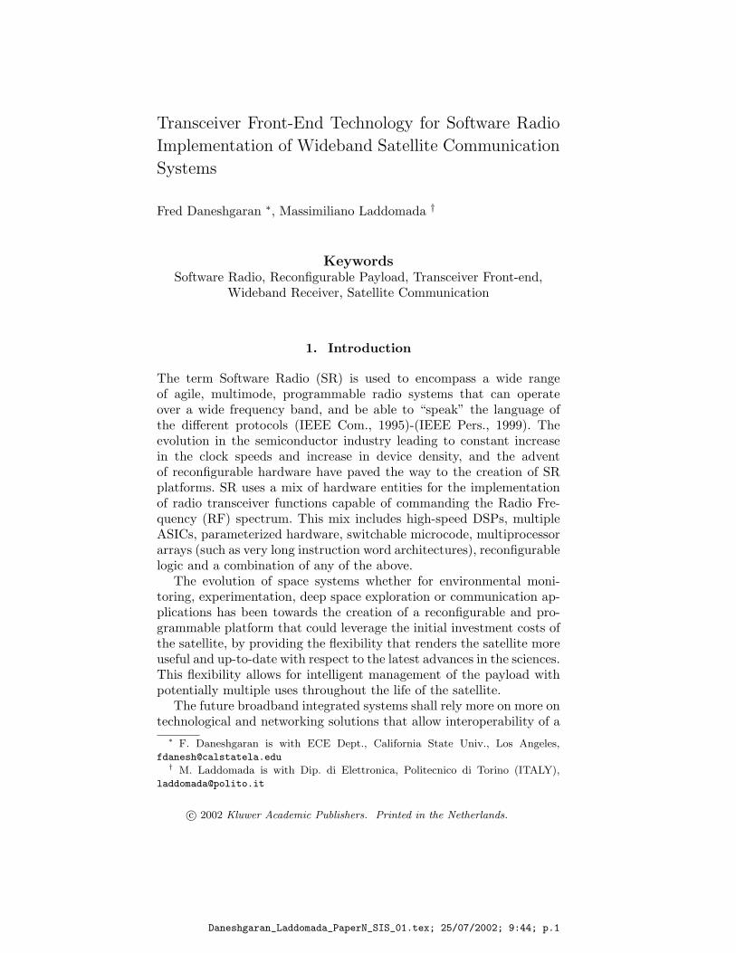
Figure 8. Overlap of the undesired signals into the useful band due to criticalsampling.
in the transform domain sampling generates replicas of the desiredsignal spectrum over a specified band, the undesired signal translatesto baseband where the useful signal lies causing aliasing.
A practical approach to remedy this problem consists in limiting thedistortion due to the undesired signal relative to the distortion causedby the ADC non-linearities in the spectrum of the signal at the outputof the ADC. Oversampling could obviously reduce the effect of largeinterfering signals close in frequency to the Nyquist bandwidth of thedesired signal.
The adjacent channel interference specifications depend on the mul-tiple access scheme adopted for the desired air interface. While inCDMA based standards there is no adjacent channel interference be-cause all coded signals cover the same bandwidth (there is howeversignificant cochannel interference present), in FDMA based air inter-faces any useful channel has several adjacent channels. In the lattercase, the receiver has to be able to detect the desired signal from abandwidth containing many interfering signals, in compliance with theSFDR requirements for the system. As an example, the GSM standardspecifies a mask showing the power level of the adjacent interferingsignals which ensures that desired channel could be detected from awideband signal with acceptable fidelity level.
3. Architecture of the Prototype Test Platform
This section outlines the development of a PC-based prototype softwareradio system designed and build utilizing a powerful front-end technol-ogy that is explored in a further section. The SR receiver is basedon a 800 MHz Pentium III processors. The operating system adopted
Daneshgaran_Laddomada_PaperN_SIS_01.tex; 25/07/2002; 9:44; p.16

17
! " #" $%
'&)(* +,-. /0+,
'& " ( +123 +4 -
576 ( 5,83 +
"
9 0: $%+%+ <;)
Figure 9. Receiver architecture.
for the workstations has been the Linux operating system because itguarantees the maximum accessibility to all the computer resources,such as device drivers for Input/Output (I/O) operations, and becauseit is shareware.
For the design presented in this paper, no kernel tuning has beenperformed to prioritize processes, although the workstations have beenprimarily used to run the software transceiver code. The system hasa 33 MHz PCI bus which is 32 bits wide. The receiver functionalitieshave been implemented in software using a high level programminglanguage. This design approach allows the transmission parameters tobe reconfigured in a simple manner. The software radio prototype hasbeen conceived to support real-time AMPS and GMSK transmissionand reception.
The high-level receiver architecture for both reception systems isshown in Fig. 9. It is composed of two main blocks, an analog radiosubsystem and a signal processing subsystem which communicates withthe front-end through an I/O interface. The receiver analog front-endis based on a wide-band delta-sigma (∆Σ) converter which converts auseful signal with RF bandwidth up to 100 MHz centered around aRF frequency up to 2 GHz from the antenna in a sampled data streamdown to baseband (i.e., direct conversion or zero IF design). The outputof this ADC converter subsequently feeds the workstation via an I/Ointerface card. This latter functionality will be discussed later, but itsmain function is to absorb processing jitters due to operation in ageneral time-shared workstation.
3.1. The Programming Environment
In order to specify the physical layer of the transceiver structure, aprogramming environment has been developed. The environment allowsreal time processing of the samples of the signal in a time driven sample-
Daneshgaran_Laddomada_PaperN_SIS_01.tex; 25/07/2002; 9:44; p.17

18
by-sample or block-by-block fashion. The environment consists of asimple programming language with semantics allowing direct definitionof the system structure, a library of processing blocks and a generalmanagement program.
The management program controls the signal flow, while the actualprocessing is performed by a sequence of processing blocks belongingto the environment library. In the management program, system pa-rameters such as the sampling rate, the bit rate and number of samplesper symbol (in case of digital transmission) are defined, and the controlvariables of various blocks are updated. The processing blocks may op-erate with samples of the complex envelope of the narrowband signals,or with real samples of baseband or quasi-baseband signals.
For the demonstrator described in this paper, two different recep-tion schemes have been considered, demonstrating the possibility ofprocessing both AMPS and GSM-like signals. The specific processingarchitecture of these two systems are described in the following.
3.1.1. Simulated AMPS Receiver SystemThe system allows continuous transmission of an FM modulated signalcontaining both an analog component (the voice signal) and a digitalcomponent (a data signal containing all the signaling information). Thevoice signal, either acquired through an external acquisition system orsynthetically generated, is added to the Manchester modulated datasignal with bit rate of 9 Kbit/s. The resulting signal is then frequencymodulated and transmitted. The modulated signal has RF bandwidthequal to 30 KHz.
The software processing includes a hard limiter, band-pass filter andfrequency demodulator. The voice signal is recovered by lowpass filter-ing of the demodulated signal, while the data signal is recovered aftermatched filtering and sampling. The sampling signal is generated byan IF rectifier clock recovery subsystem, composed of an envelope de-tector, tuned resonator and timing generator. Four different frequencydemodulation techniques have been implemented, namely (1) directevaluation of the instantaneous frequency; (2) PLL based frequencydemodulation; (3) differentiator followed by amplitude demodulation;and (4) correlation receiver. The four structures achieve very similarprocessing speeds and signal-to-noise ratio performances. Maximum,minimum and average processing speed in samples per second of theAMPS receiver are reported in Table III.
Referring to Fig. 9, the wideband ADC converter front-end outputstwo sample streams at a constant rate, one for the in-phase componentand the other for the quadrature component of the signal around thecarrier (i.e., samples of the complex envelope of the information bearing
Daneshgaran_Laddomada_PaperN_SIS_01.tex; 25/07/2002; 9:44; p.18

19
!
"# $% & '
(*)+ ( ,-./
Figure 10. Block diagrams of the GSM-like receiver implemented in software.
baseband signal). The I and Q samples each have a resolution of 14bits. The ADC converter has an embedded down-conversion systemwhich outputs the samples of the input signal directly in baseband. Thisapproach has the advantage of avoiding the need for rate conversionfilters in the succeeding signal processing units.
Subsequently, the I/O interface captures the I and Q samples, col-lecting them in a block of 32 bit words. The functionality necessary forperforming data transfers is embedded in the I/O board. The collecteddata is subsequently divided into their in-phase and quadrature com-ponents via software, through logic operations such as logical AND andShift acting on bits.
The data, grouped in blocks of 32 bit samples by the I/O interface,are transferred to the processor through the 32 bit PCI-bus using theDirect Memory Access (DMA) transfer mode. In this manner, whilethe digital signal processing routines are processing the AMPS datastream of the previous data block, a new block of data is transferred tothe user space. Note that the signal processing operations are strictlyrelated to I/O, so that the former always has a block of sampled datato process. This approach guarantees the use of the whole PCI bus.
3.1.2. Simulated GSM-like SystemIn the simulated GSM-like system, the attention has been focusedon the reception of a binary GMSK modulated signal. The receiverarchitecture is depicted in Fig. 10. The software processing includesa band-pass filter, a frequency demodulator, a low-pass filter and asampler. The sampling signal is generated by a Maximum Likelihoodtiming estimator. The receiver uses 5 samples per symbol and thereforeruns at a speed larger or equal to 203×5 = 1015 Ksamples/s. Maximum,minimum and average processing speed in samples per second of theGSM-like receiver are reported in Table III.
All the I/O data transfers are performed in a manner similar to thatof the AMPS demonstrator.
Daneshgaran_Laddomada_PaperN_SIS_01.tex; 25/07/2002; 9:44; p.19

20
Table III. Processing speeds in Ksamples/s for the simulatedAMPS and GSM-like systems.
Speed [Ksamples/s] Average Maximum Minimum
GSM-like 1200 1300 1050Receiver
AMPS 1700 1800 1200Receiver
3.2. The Front-End
The transceiver front-end is powered by delta-sigma (∆Σ) data con-verter technology that is capable of operating at speeds in excess of2 GHz. The process of frequency translation is built into the archi-tecture of the ADC and DAC converters. Initial prototype chips havebeen fabricated using 0.6 µm GaAs MESFET technology from VitesseSemiconductor, Inc. Additional chips have been developed using SiGetechnology, which has the advantage of being able to be fabricated onthe same silicon substrate as conventional CMOS VLSI circuits.
3.2.1. Overall StructureThe block diagram of the software radio front-end showing the crit-ical components is shown in Fig. 11. The use of multiple antennasat the transceiver front-end is more a technological requirement thana system constraint. Generally speaking, antennas and tuned circuitsat the front-end are efficient constant Q elements (Q is the qualityfactor of the tuned resonator). Using present technology, it is verydifficult to construct a single antenna element and efficiently couplethe received power to the Low-Noise-Amplifiers (LNAs) and transmitpower from the Power-Amplifiers (PAs) to the antenna over a frequencyband ranging several decades. Same argument holds for the design ofLNAs and Power-Amplifiers. Hence, from a practical point of view itis essential to have multiple antennas and corresponding analog front-end elements to efficiently receive and transmit signals over a band offrequencies spanning several decades.
In the block diagram of Fig. 11, we show high speed Transmit/Receive(T/R) switches. This is not meant to be restrictive in any sense and
Daneshgaran_Laddomada_PaperN_SIS_01.tex; 25/07/2002; 9:44; p.20

21
Figure 11. The global architecture of the front-end.
diplexers could easily be accommodated in the structure. As a matterof practice, efficient means of coupling signal power to the antenna andreceiving power from the antenna is only possible if there is sufficientisolation between the transmit and receive ports. This is typically doneby either switching between transmit and receive modes, or using simul-taneous transmission and reception on two different frequency bandswith sufficient separation, using a diplexer. Obviously, we may alsoemploy a combination of the two techniques. Other potentially usefulelements such as roofing filters and Automatic Gain Control (AGC)amplifiers are not shown for simplicity.
In the receive path of Fig. 11 we show a band selector which es-sentially switches among the multiple frequency bands allocated byFCC for different applications. The analog to digital conversion be-yond this point is performed using the proprietary high-speed ADCfrom TechnoConcepts, Inc. (www.technoconcepts.com) that performsprecision down-conversion of the signal. The signal processing afterband selection may be described as follows:
− the In-phase and Quadrature (I&Q) paths are distinct and areclocked by very precise in-phase and quadrature clock signals. The
Daneshgaran_Laddomada_PaperN_SIS_01.tex; 25/07/2002; 9:44; p.21

22
Figure 12. Block diagram of the ∆Σ A/D converter.
clock signals themselves are generated from a frequency synthesizerthat generates a signal at twice the center frequency of the bandbeing digitized. A precise phase splitter generating the desired I&Qclock signals follows the frequency synthesizer;
− the bandwidth of the ADC converter is very large and usuallyseveral frequency channels associated with a given standard aredigitized in one shot. In order to separate out distinct frequencychannels, a channelizer which could be in the form of an analysisfilter-bank is used to generate complex data streams correspondingto the samples of the complex envelopes of the signals in differentfrequency bands. Resampling, rescaling, and phase correction ofthe digitized waveforms can either be performed on the compositesignal just prior to the channelizer, or on individual channels afterthe channelizer;
− the combined precision down-conversion using a single master clockand subsequent channelization, resampling, rescaling, and phasecorrection operations essentially allow the front-end to pick up sig-nals associated with different air-interfaces. The oversampling fac-tor of the signal is application dependent but at the very minimum,5 samples per symbol are generated and subsequently processed;
− channel selection operations and further signal processing is per-formed after the channelizer but is not shown in the figure forsimplicity.
The transmit side of Fig. 11 essentially performs the inverse operationas that of the receive side. Inclusion of the frequency synthesizer andmulti-phase clock generator in the transmit block diagram allows for
Daneshgaran_Laddomada_PaperN_SIS_01.tex; 25/07/2002; 9:44; p.22

23
possible simultaneous operation of the unit in both transmit and receivemodes possibly over two distinct frequency bands and possibly usingdifferent antennas.
3.2.2. ∆Σ converter architectureThe high speed delta-sigma (∆Σ) modulator A/D with embedded pre-cision down-conversion is a classic design with several modifications andintegration of critical functions on a single substrate to achieve signif-icant performance improvements over traditional designs. The blockdiagram of the ∆Σ modulator is shown in Fig. 12. The main featuresof the design are:
− the complementary amplifier provides a negatively and positivelyamplified versions of the input signal to the switching port. Preci-sion down-conversion is essentially achieved by commutation andsubsequent filtering in the rest of the modulator;
− the ADC resolution is determined by the oversampling factor andthe loop filter order. More precisely, 1.5,2.5,3.5, and 4.5 bits ofresolution per octave oversampling ratio is achievable for loopfilters from first to fourth order. The commutation frequency isthe same as the center frequency of the band that is to be down-converted to near DC and digitized. As an example, for a secondorder loop, at a center frequency of 1 GHz, and for a RF bandwidthof 10 MHz around the center frequency, the oversampling ratio is100 or 6.6 octaves. The resulting resolution is greater than 16 bitsresulting in about 99 dB of raw dynamic range. Down-conversionvia commutation greatly enhances the dynamic range and allowsfor precise control over the clocking phase of the in-phase andquadrature components;
− down-conversion of the signal to a frequency near DC but not toDC allows for utilization of digital filters to eliminate DC offseteffects of the analog components in down stream signal processingstages;
− the loop filter is based on simple analog designs greatly enhanc-ing the ADC bandwidth and completely eliminating the need forSwitched Capacitor Filters (SCF). The problem of SCF is thatthey cause aliasing and hence interference. Eliminating the SCF,the ADC can use continuous time filter with lower order and allowsoperation of the loop at much higher frequencies;
Daneshgaran_Laddomada_PaperN_SIS_01.tex; 25/07/2002; 9:44; p.23

24
− the ADC uses commutation for down-conversion of the RF signalas opposed to sub-sampling which requires tremendous precisionand femto-second pulses to achieve high resolution;
− all the components of the ADC converter are integrated on a singlesubstrate using novel circuit solutions completely avoiding the needto exit the IC reducing costs, size, and eliminating the problemwith circuit non-idealities;
− a novel super-linear commutating amplifier is used at the inputstage as the core of the design;
− the overall design uses a current steering technique based on Galium-Arsenide MESFETs and Silicon-Germanium devices resulting inconstant power dissipation regardless of the center frequency ofthe signal to be down-converted and digitized.
The architecture of the Digital to Analog Converter (DAC) is muchthe same as a classic ∆Σ demodulator but switching via logic gatesis used for up-conversion of the baseband signal to around the carrierfrequency.
3.3. The I/O Interface
The main problem that arises using a workstation as the software radioplatform concerns the rate at which transceiver operations are to beperformed. For real-time operation, the data flux from the ADC withembedded precision down-conversion, and to the DAC with embeddedprecision up-conversion is constant. However, as noted earlier, since thetransceiver operation is run in software and is under the control of theLinux kernel, the rate at which data is processed by the workstationis not constant. In order to avoid any kind of jitter due to rate fluc-tuations for task scheduling and memory management operations, anI/O interface board has been used. This board is a PCI form factorultra high-speed digital I/O card and consists of 32 bit digital inputand output channels. Due to the high rate by which it executes datatransfers, this board is particularly suited for high-speed digital I/Oapplications. It performs the data transfer using bus mastering DMAvia a 32 bit PCI bus architecture. The maximum data transfer rate is80 MHz. Use of DMA transfer mode allows the main processor loadto be reduced, since the data transfer takes place in background, whilethe main processor performs digital signal processing on the previousinput data stream. The use of an I/O board has the effect of elimi-nating the need for any kind of timing synchronization between theanalog front-end and the main processor. The I/O board decouples the
Daneshgaran_Laddomada_PaperN_SIS_01.tex; 25/07/2002; 9:44; p.24

25
AnalogFront-End
I
Q
data stream
I/O Interface board
16 bit 32 bit
32 bit
double buffer
halfdoublebuffer
32 bitPCI-bus
UserSpace
DMAtransfermode
Figure 13. Block diagram of the I/O system for the receiver side.
instantaneous rate by which the analog front-end produces data fromthe rate by which the previous block of data are processed by the CPU.
The board has a set of C-language routines that makes all datatransfer management operations simple. The architecture of the I/Osystem for the receiver side is shown in Fig. 13. A similar structureis used for the transmitter side of the transceiver. The only differenceconcerns the direction of data flow.
The data transfer occurs at the ADC word sample rate (since thearchitecture of the ADC is that of delta-sigma, the raw sample rate ismuch larger than the word rate at the output) by using the externalclock mode. This operational mode is mastered by the clock sourcecoming from the ADC converter. In particular, it is the same clockused by the ADC after the decimation filtering of the signal. The I/Oboard samples a 32 bit input word on the positive edge of the clock. Inthis manner it is guaranteed that I/O board samples a valid data fromthe ADC converter.
The continuous data transfer in real-time mode is guaranteed by thedouble-buffered asynchronous continuous digital input programmingscheme. The principle behind this operation mode is to use a circularbuffer logically divided into two equal halves. The buffer length is setbefore every input transfer starts in order to guarantee real-time op-eration. Before the effective receiving phase begins, the I/O board isset to support digital input operations in an asynchronous mode. Theterm asynchronous refers to the fact that the data transfer takes placeonly after a certain amount of data has been transferred to the inputboard from the receiver front-end.
Daneshgaran_Laddomada_PaperN_SIS_01.tex; 25/07/2002; 9:44; p.25

26
3.3.1. Determination of the circular buffer sizeThe key factor behind the determination of the buffer size concerns theneed of guaranteeing real time transmission with acceptable delays. Theoperation rate is chosen so that the digital signal processing executiontime in the workstation matches the time by which the I/O deviceboard fills half of the circular buffer (it is also possible to transferdata at a rate less than the capacity of the digital signal processingstage). This condition is a system level constraint and assures thatthe signal processing routines always have correct samples to process.In other words, the condition assures that the Input data transfer isnot a bottleneck for the overall system. As an example, consideringthe AMPS receiver, we may calculate that an input signal of usefulbandwidth equal to 30 kHz produces an input data rate of about75 ksample
s if the oversampling factor is equal to 5 samples for inputsignal period and if the input signal is translated to baseband beforebeing sampled by the front-end. This rate corresponds to a throughputof about r = 13.3 µs
sample , while the digital signal processing executiontime is equal to 0.58 µs
sample . This means that the platform is capableof correctly processing one AMPS channel.
In Fig. 14, the solid curve depicts the average time to transfer datafrom the receiver front-end to the user space, while the dotted curvereflects the average time required to process the data with the AMPSreceiver, which is a constant value, plus the time to transfer data to thespeaker. The average transfer times for both curves has been evaluatedas a function of the buffer size, by averaging over one hundred transfers.From this figure, it is possible to observe that the time to transferdata is a decreasing function of the buffer size. This is due to thefact that a certain amount of time for transferring data is independent(within certain limits) of the total number of data samples transferred.Hence, increasing the buffer size, the overhead time associated withthe intrinsic time for data transfer with the I/O board is reduced foreach transferred sample. The dotted curve is increasing slowly becausethe time to transfer processed data to the speaker increases when moredata are transferred. However, this latter time is much smaller thanthe average time used for data transfer from the input boundary to theuser space. Of course, the drawback of using larger sized buffers is theoverall system latency which must be within tolerable limits.
The time spent for transferring the data processed by the softwareroutines, to the audio board falls in the range of [0.1175 µs
sample ; 0.175 µssample ]
for buffer size in the range of [2000; 20000] samples.
Daneshgaran_Laddomada_PaperN_SIS_01.tex; 25/07/2002; 9:44; p.26

27
2 4 6 8 10 12 14 16 18 200.5
1
1.5
2
2.5
3
3.5
4
4.5
5
5.5
buffer size (x103 samples)
Ave
rage
Tim
e in
mic
rose
cond
s
Figure 14. Average times.
In order to guarantee real time operation, the following equation,valid for both AMPS and GMSK receivers, must be met:
tproc + tspeaker ≥ tDI (2)
tproc + tspeaker ≤ r (3)
where, tproc is the average time spent by the software routines forprocessing an input sample, tspeaker is the average time spent for trans-ferring a processed data sample from the user space to the audio board,tDI is the average time spent to transfer half of the double buffer fromthe input boundary to the user space. Finally, r is the throughputexplained at the beginning of this section. All specifications of time havebeen normalized with respect to the buffer size. For the AMPS receiver,this average time is about 0.58 µs
sample , no matter what the buffer size.This value has been obtained by performing signal processing on 100input data blocks. Note that, if Eq. 3 is not satisfied, the system maydrop the data incoming from the front-end or may change the rate bywhich the processed samples are transferred to the audio board.
In the case of the AMPS receiver, taking into account the data shownin Fig. 14 and the time for data transfer to the speaker, a minimumbuffer size of 18000 samples is needed in order to comply with Eq. 2.This value is actually half of the size of the circular buffer. Choosinga greater buffer size, it is possible to reduce the overhead time due tothe call to the software routines, but at a price of increased latency.
An analogous discussion holds valid for the GMSK receiver. Theonly difference is that in this case, the processing time for each samplechanges while all other timing constraints remain the same. All time
Daneshgaran_Laddomada_PaperN_SIS_01.tex; 25/07/2002; 9:44; p.27

28
evaluations have been made by using the C-shell time (Turletti et al.,1999), which guarantees that the whole CPU is used for the applicationunder examination.
4. Conclusion
In this paper we have attempted to draw a potential evolutionary pathfor the transceiver architectures based on the SR technology that maybe employed in the future broadband satellite communication systems.There are ample economic and practical reasons for such an evolu-tionary path to come to fruition. Subsequently, we have focused onthe architecture of the transceiver front-end that still remains the keytechnological bottleneck to the proliferation of SR transceivers for boththe space and terrestrial applications. Various architectures for digitalreceivers have been presented along with analysis of limitations andadvantages of each scheme. Finally, we have presented the architectureof a prototype SR receiver we have designed, build and tested usinga novel front-end technology based on a promising architecture thatcombines frequency translation and sampling. High level details of theADC that is at the core of our design has been presented along withsample processing rates we have been able to achieve for AMPS likeand GSM like signals.
References
J. Mitola, “The Software Radio Architecture”, IEEE Communications Magazine,Vol.33 No.5, pp.26–38, February 1995.
IEEE Communications Magazine, “Special Issue on Software Radio”, Vol.37, No.2,pp.82–112, February 1999.
“Special Issue on Software Radio”, IEEE Journal on selected areas in communica-tions, Vol. 17, No.4, April 1999.
IEICE Trans. Commun., “Special Issue on Software Defined Radio and its Technolo-gies”, June 2000.
IEEE Personal Communications, “ Special Issue on Software Radio”, August 1999.J. Sevenhans, B. Verstraeten, S. Taraborrelli, Trends in Silicon Radio Large Scale
Integration: Zero IF Receiver! Zero I & Q Transmitter! Zero Discrete Passives!,IEEE Communications Magazine, January 2000.
R. H. Walden, Analog-to-Digital Converter Survey and Analysis, IEEE JSAC, Vol.17, No. 4, April 1999.
GSM Recommendation 05.05, Radio Transmission and Reception, March 1996.A. A. Abidi, Direct-Conversion Radio Transceiver for Digital Communications,
IEEE Journal of Solid-State Circuits, Vol. 30, No. 12, December 1995.W. Namgoong, T. H. Meng, Direct-Conversion RF Receiver Design, IEEE Transac-
tions on Communications, Vol. 49, No. 2, March 2001.
Daneshgaran_Laddomada_PaperN_SIS_01.tex; 25/07/2002; 9:44; p.28

29
D. Haspeslagh et al., BBTRX: A Baseband Transceiver for a Zero IF GSM HandPortable Station, Proceedings of Custom IC Conf., San Diego, CA, 1992.
H. Tsurumi, Y. Suzuki, Broadband RF Stage Architecture for Software-Defined Radioin HandHeld Terminal Applications, IEEE Communications Magazine, February1999.
T. Turletti, H. J. Bentzen, D. Tennenhouse, “Toward the Software Realization of aGSM Base Station”, IEEE Journal on selected areas in communications, Vol. 17,No.4, pp.603–612, April 1999.
Daneshgaran_Laddomada_PaperN_SIS_01.tex; 25/07/2002; 9:44; p.29