
Training CST 1
48
CST MICROWAVE STUDIO Overview Berezin Maksim Ben-Gurion University. Course “Antennas and Radiation”.
-
Upload
rameshdurairaj -
Category
Documents
-
view
76 -
download
0
description
cst software
Transcript of Training CST 1

CST MICROWAVE STUDIO
Overview
Berezin Maksim
Ben-Gurion University.
Course “Antennas and Radiation”.

Ctrl: Rotation
Shift: In-plane rotation
Ctrl+Shift: Panning
View Options
Set view to „Rectangle zoom“: Use mouse to select area to zoom.
Change the view by dragging the mouse while pressing the left button anda key:
SPACE-bar: Reset View (undo zoom)
Shift – SPACE:Zooms into selected shape
Other useful options:
Roll (middle) mouse button: dynamic zoom

Primitives
Brick
Sphere
Cylinder
EllipticalCylinder
Extrusion
Cone Torus
Rotation
Hints:• Press TAB-key to enter a point numerically.• Press BACKSPACE to delete previous picked point

Picks
Pick a point, an edge or an area in the structure
1. Activate the tool (via Icon, Menu Objects->Pick or Shortcut)2. Double click on the point, edge or area
Select corner point (P)
Select midpoint of straight edge (M)
Select centerpoint of circle(click on circle) (C) Select centerpoint of area
(click on area) (A)
Select edge (E) Select area (F)
Select point on circle(click on circle) (R)
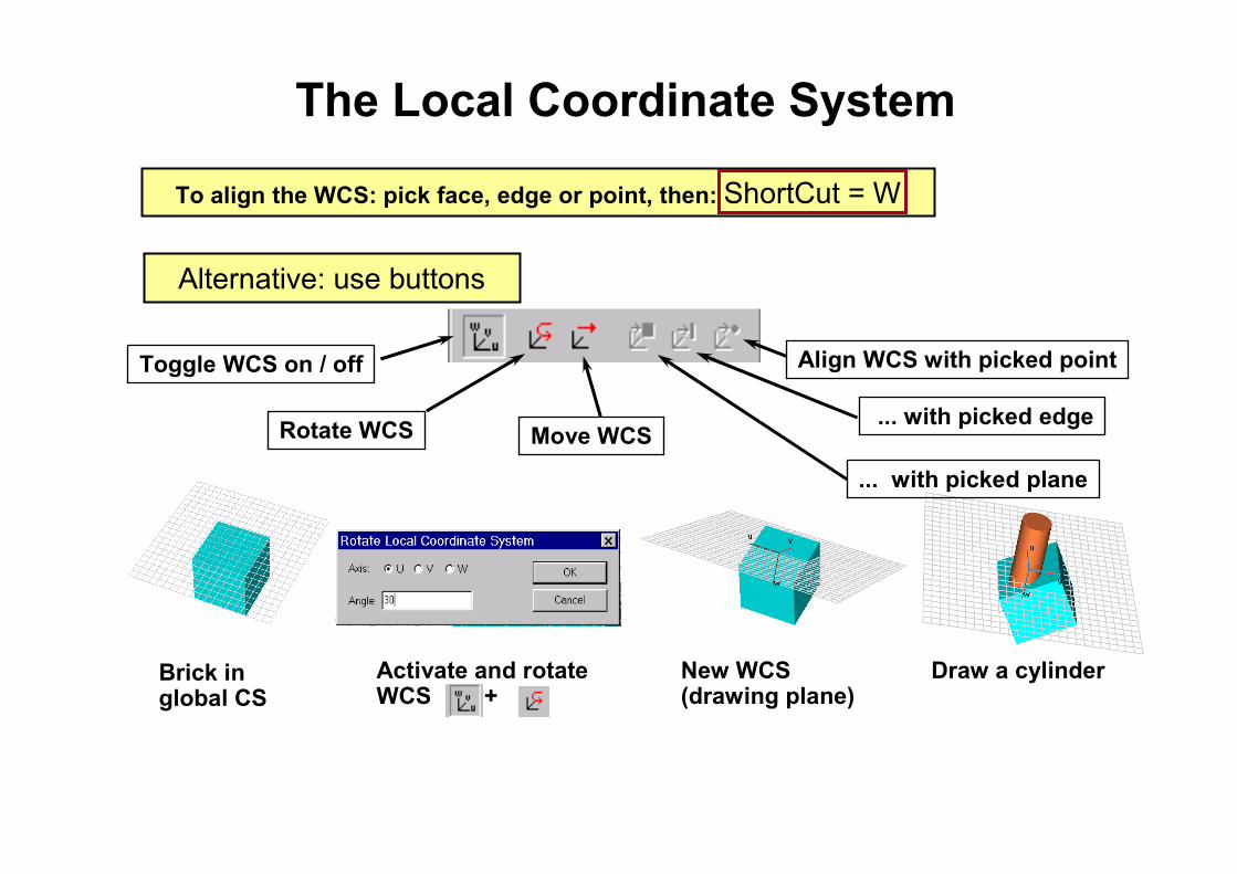
The Local Coordinate System
Brick inglobal CS
Activate and rotateWCS +
New WCS(drawing plane)
Draw a cylinder
Toggle WCS on / off
Rotate WCS Move WCS
... with picked plane
... with picked edge
Align WCS with picked point
To align the WCS: pick face, edge or point, then: ShortCut = W
Alternative: use buttons

Boolean Operations
Subtractbrick - sphere
Addsphere + brick
Sphere (new shape)
and Brick (old shape)
Insertmodifies old shape
brick / sphere
Trimmodifies new shape
sphere / brick
Intersect
brick * sphere

Trace from Curve
Step 1: New Curve
Step 2: New Polygon
Step 3: Trace from Curve

Rotation of Profile
• Select icon and enter profile• Avoid intersections
• Press BACKSPACE to deleteprevious picked point
• Double click corner points to move them around

Loft-Operation
Loft-Operation
Two picked faces,
to be connected by new shape
The new shape’s profile
is morphed from the first
picked face into the second.
Objects -> Loft...
NOTE: Loft is even possible,
if faces are not parallel

Blend and Chamfer Edges
Blend
Chamfer
Difference !
ONE Blend-Operation:
All 3 edges picked
THREE Blend-Operations:
Each edge blend alone
For many edges,
use SHIFT-E (picks
closed edge chain)
Blend

Shell-Operation
1. Select component1
2. Objects ->
Merge Materials on Component
1. Picked faces, to be open after shelling
2. Select solid1, to be shelled
solid2
solid3
solid1
Combine to ONE shapesolid1
Picked faces are open
after Shelling-Operation
Objects -> Shell...
TASK: Waveguide-Bend, consisting of
three shapes, should be shelled

Definition of Ports

Ports for S-parameter computation
Discrete Ports
(lumped element)
Waveguide Ports
(2D eigenmode solver)
Input: Area for eigenmode solution
Output: E and H-Pattern,
Line Impedance,
Prop.constant (beta+alpha)
Input: Knowledge of TEM-Mode
Line Impedance
Output: Voltage and Current
• Discrete ports can be used for TEM-like modes, not for higher modes (fcutoff>0).
• Waveguide Ports deliver better match to the mode pattern
as well as higher accuracy in S-Parameters.

Discrete PortsS parameter port
~Ri
or Ri
2. Voltage port 3. Current
~
Coaxial Microstrip Coplanar WaveguideStripline

Discrete Port Definition
Select Port Type
and Impedance
pick 2 points
(or)
1 point and a face
(or)
enter coordinates
(not recommended)

Discrete Port DetailsMesh
1. The port is the cone on the mesh edge
2. That edge must be a dielectric edge
3. The wires attach the port to the structure
In metal Open

Waveguide Port Definition
Pick Edge Pick Face
Also possible: any combination
of pick points, edges, faces

Coaxial Microstrip Hollow WaveguideCoplanar Waveguide
In addition to pick point, Full Plane
or Free Coordinates can also be
specified
For Phase Deembedding
Number of desired Higher Order
Modes
For Separation of Degenerate
Modes in Circular Waveguides
Waveguide Port Definition

NO, Too small YES, Good NO, Unnecessarily large
Waveguide Port Details
Port must be large enough to cover the
fields of the port mode of interest.
3 mesh cells
Time Domain: Geometry must be
homogenous for 3 mesh cells
Frequency Domain: Internal port
must be backed by PEC

Port Impedance Evaluation
NO, Too SmallNO, Too Big
YES, Good

Port Definition - Microstrip Line
2) Enter Port menu
3) Adjust additional port space
(+- 5 width, +5 height)
1) Pick 3 Points
width height

Boundary Conditions

Boundaries
CST MWS uses a rectangular grid system, therefore also the complete calculation domain is
of rectangular shape => 6 boundary surfaces have to be defined at the minimum and
maximum position in each co-ordinate direction (xmin, xmax, ymin, ymax, zmin, zmax).
Example: T-Splitter
xmin
xmax
ymin
ymax
zmin
zmax

Boundary settings (1)
7 different settings are available

Boundary settings (2)
Electric boundaries (Default setting): No tangential electric field at surface.
Magnetic boundaries: No tangential magnetic field at surface. Default setting
for waveguide port boundaries.
Open boundaries: Operates like free space – waves can pass this boundary with
minimal reflections. Perfectly matched layer (PML) condition.
Open add space boundaries: Same as Open, but adds some extra space for
farfield calculation (automatically adapted to center frequency of desired
bandwidth). This option is recommended for antenna problems.
Conducting wall: Electric conducting wall with finite conductivity (defined in
Siemens/meter).

Boundary settings (3)
Periodic boundaries: Connects two opposite boundaries so that the calculation
domain is simulated to be periodically expanded in the corresponding direction.
Thus it is necessary that both boundaries facing each other are always indicated
as periodic. The resulting structure represents an infinite expanded antenna
pattern, phased array antennas. F! Hex mesh, T! + 0 phase shift
Unit Cell: Used with F! Solver, Tet mesh, similar to F! Periodic
boundary with Hex mesh. A two dimensional periodicity other than in
direction of the coordinate axes can be defined. If there are open boundaries
perpendicular to the Unit Cell boundaries, they are realized by Floquet
modes, similar to modes of a wave guide port .
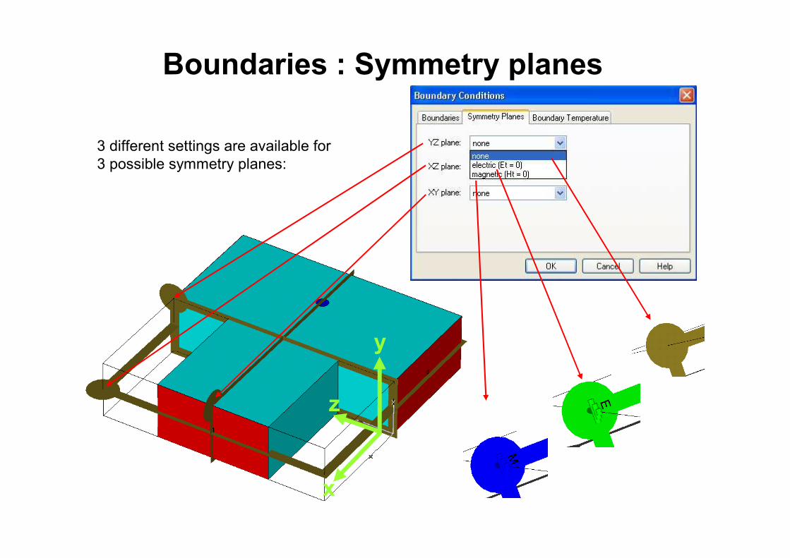
Boundaries : Symmetry planes
3 different settings are available for
3 possible symmetry planes:
z
y
x

Materials

Normal: General material model Typically
used for dielectric materials
Basic Materials
∞=σPEC: Perfect Electric Conductor
Anisotropic: εεεε and µµµµ are directionally dependent
Lossy Metal: Conductor
∞≠σ
Corrugated wall: Surface impedance
Ohmic sheet: Surface impedance [Ω/ ]

Lossy Metal
Why is it required?
Sampling of skin depth would require very fine mesh steps at the metal
surface and definining conductor as a normal material
(skin depth for copper at 1 GHz approx. 2 um)
This results in a very small timestep, which leads to a very long
simulation time
Solution:
1D Model which takes skin depth into account without spatial sampling.

Lossy Metal

Solver Selection
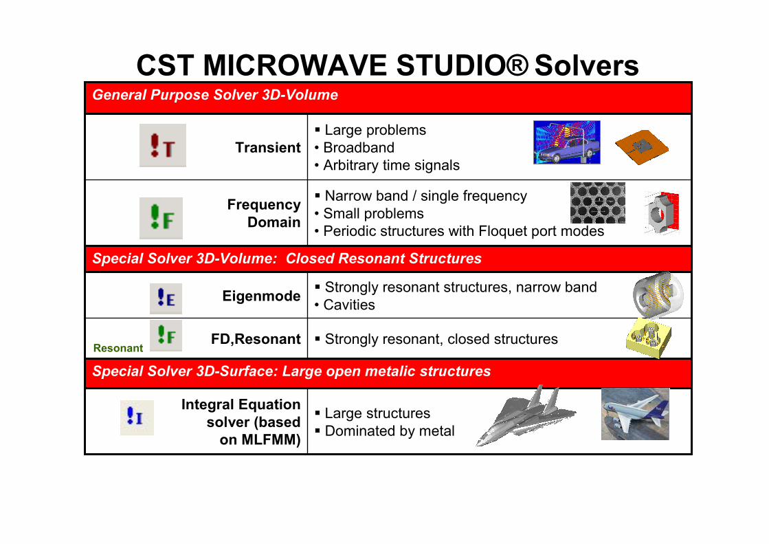
CST MICROWAVE STUDIO® Solvers
Large structures
Dominated by metal
Integral Equation
solver (based
on MLFMM)
Special Solver 3D-Surface: Large open metalic structures
Special Solver 3D-Volume: Closed Resonant Structures
Strongly resonant, closed structuresFD,Resonant
Strongly resonant structures, narrow band
• CavitiesEigenmode
Narrow band / single frequency
• Small problems
• Periodic structures with Floquet port modes
Frequency
Domain
Large problems
• Broadband
• Arbitrary time signals
Transient
General Purpose Solver 3D-Volume
Resonant

Transient Solver Introduction
• Hexahedral mesh only
• Time and Frequency Domain Results
• All frequencies in one simulation
• Begin with no energy inside calculation domain
• Inject energy and step through time
• As time progresses, energy inside calculation domain decays
• When energy decays “far enough,” the simulation stops

Overview
• Arbitrary input signal
• Inject energy and watch it leave
• Solve for unknowns without matrix inversion
• Hexahedral Mesh: Broadband meshing and results
• Simulation is performed on a port-by-port basis
• Smaller mesh cells = longer solve times
• Energy storage for high Q structures prolongs simulation time
!T – Time Domain Solver
The transient solver is very robust
and can handle most applications.
Well suited applications: Broadband,
electrically large structures.
Highly resonant, electrically small
structures may be better suited to the
frequency domain solver.

Frequency Solver Introduction
• Simulation performed at single frequencies
• Broadband Frequency Sweep to achieve accurate S-Parameters
• very robust automatic mesh refinement (easy to learn)
2nd General Purpose Solver (besides Time Domain)

!F – Frequency Domain Solver
The frequency domain solver is very robust and can handle most applications.
Well suited applications: Narrowband, electrically small structures.
Limited computational resources make it necessary to use the time domain
solver for electrically large structures.

!E – Eigenmode Solver
The eigenmode solver is a very specialized tool for closed
cavities. No s-parameters are generated, only eigenmodes
which are single frequency results.
Well suited applications: Narrow band, resonant cavities.

Meshing: The Basics

Mesh Generation
Mesh view
(on / off)
Orientation of
mesh plane
(Shortcut x/y/z)
In-/Decrease
index of cut planeUpdate
Properties
Fixpoint list
Mesh control points

Smallest mesh step determines simulation speed !
Define size of the
biggest mesh step
Limitation for the
smallest mesh step
Global Mesh Properties- Hexahedral
Lines Per Wavelength defines the minimum
number of mesh lines in each coordinate direction
based on the highest frequency of evaluation.
Lower Mesh Limit defines a minimum distance
between two mesh lines for the mesh by dividing
the diagonal of the smallest bounding box face by
this number.
Ratio Limit defines ratio between the
biggest and smallest distance between
mesh lines. Increase for mesh quality
when high aspect ratios exist, e.g.
edge coupled microstrip.
Alternative to ratio limit, the Smallest
mesh step can be entered directly as
absolute value rather than defining it
relatively via biggest mesh step and
ratio limit.

1-3 meshlines(dep. on thickness)
1-2 meshlines
Required Initial Discretization
1) Microstrip + cpw
2) Coaxial
Required meshlines:
• coax-center
• INNER radius of dielectric
• OUTER radius of dielectric
Required meshlines:
• each straight PEC-edge
(for each slot + stripline)(metal thickness does not need 2 meshlines)

CST MWS - Standard workflow
Choose Project Template
Parameters + Geometry + Materials
Ports
Frq-Range + Boundaries / Symmetries
Monitor Definition
Quick Check Meshing
Run Simulation

Analyze 1D Results
S Parameter
Energy
Port Signals

Analyze 2D/3D Results

Electric Field @ 10GHz

Far Field @ 10GHz

Copy / Paste of Result Curves
Signal plots and farfield curves can now be copied by using standard copy / paste


![TRAINING PLAN - MARAMA€¦ · Training Plan PURPOSE ... ACTION ITEM 1 – ASK CENSERA WHAT THIS IS. ... “Advanced Inspector Training” [NETI CST-309] V. C. OMPLIANCE . C.](https://static.fdocuments.in/doc/165x107/5b0a76ec7f8b9a99488c3475/training-plan-plan-purpose-action-item-1-ask-censera-what-this-is-.jpg)


