TPS7B69xx 150-mA, 40-V Ultralow-Quiescent-Current LDO Sheets/Texas... · · 2017-09-071• 4-V to...
21
GND 10 μF 4.7 μF V bat V reg V O V I IN OUT Copyright © 2016, Texas Instruments Incorporated TPS7B69xx Product Folder Sample & Buy Technical Documents Tools & Software Support & Community An IMPORTANT NOTICE at the end of this data sheet addresses availability, warranty, changes, use in safety-critical applications, intellectual property matters and other important disclaimers. PRODUCTION DATA. TPS7B6933, TPS7B6950 SLVSDI2 – APRIL 2016 TPS7B69xx 150-mA, 40-V Ultralow-Quiescent-Current LDO 1 1 Features 1• 4-V to 40-V Wide V I Input Voltage Range With up to 45-V Transient • Maximum Output Current: 150 mA • Low Quiescent Current (I Q ): – 15 μA Typical at Light Loads – 25 μA Maximum Under Full Temperature • 450-mV Typical Low Dropout Voltage at 100 mA Load Current • 10-mV Line Regulation Maximum • 20-mV Load Regulation Maximum • Stable With Low-ESR Ceramic Output Capacitor (2.2 μF to 100 μF) • Fixed 3.3-V and 5-V Output Voltage Options • Integrated Fault Protection: – Thermal Shutdown – Short-Circuit Protection • Packages: – 5-Pin SOT-23 Package – 4-Pin SOT-223 Package 2 Applications • E-meters, Water Meters and Gas Meters • Appliances and White Goods • Fire Alarm, Smoke Detector • Medical, Health, and Fitness Applications 3 Description The TPS7B69xx device is a low-dropout linear regulator that operates at up to 40-V V I . With only 15-μA (typical) quiescent current at light load, the device is applicable for standby microcontrol-unit systems, especially for always-on applications like e- meters, fire alarms, and smoke detectors. The devices have integrated short-circuit and overcurrent protection. The TPS7B69xx device operates over a –40°C to 105°C temperature range. Device Information (1) PART NUMBER PACKAGE BODY SIZE (NOM) TPS7B6933 TPS7B6950 SOT-223 (4) 6.50 mm × 3.50 mm SOT-23 (5) 2.90 mm × 1.60 mm (1) For all available packages, see the orderable addendum at the end of the datasheet. Typical Application Schematic
Transcript of TPS7B69xx 150-mA, 40-V Ultralow-Quiescent-Current LDO Sheets/Texas... · · 2017-09-071• 4-V to...
GND10 µF 4.7 µF
VbatVreg
VOVI
IN OUT
Copyright © 2016, Texas Instruments Incorporated
TPS7B69xx
Product
Folder
Sample &Buy
Technical
Documents
Tools &
Software
Support &Community
An IMPORTANT NOTICE at the end of this data sheet addresses availability, warranty, changes, use in safety-critical applications,intellectual property matters and other important disclaimers. PRODUCTION DATA.
TPS7B6933, TPS7B6950SLVSDI2 –APRIL 2016
TPS7B69xx 150-mA, 40-V Ultralow-Quiescent-Current LDO
1
1 Features1• 4-V to 40-V Wide VI Input Voltage Range With up
to 45-V Transient• Maximum Output Current: 150 mA• Low Quiescent Current (IQ):
– 15 µA Typical at Light Loads– 25 µA Maximum Under Full Temperature
• 450-mV Typical Low Dropout Voltage at 100 mALoad Current
• 10-mV Line Regulation Maximum• 20-mV Load Regulation Maximum• Stable With Low-ESR Ceramic Output Capacitor
(2.2 µF to 100 µF)• Fixed 3.3-V and 5-V Output Voltage Options• Integrated Fault Protection:
– Thermal Shutdown– Short-Circuit Protection
• Packages:– 5-Pin SOT-23 Package– 4-Pin SOT-223 Package
2 Applications• E-meters, Water Meters and Gas Meters• Appliances and White Goods• Fire Alarm, Smoke Detector• Medical, Health, and Fitness Applications
3 DescriptionThe TPS7B69xx device is a low-dropout linearregulator that operates at up to 40-V VI. With only15-µA (typical) quiescent current at light load, thedevice is applicable for standby microcontrol-unitsystems, especially for always-on applications like e-meters, fire alarms, and smoke detectors.
The devices have integrated short-circuit andovercurrent protection. The TPS7B69xx deviceoperates over a –40°C to 105°C temperature range.
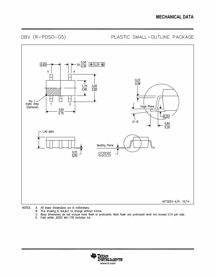
Device Information(1)
PART NUMBER PACKAGE BODY SIZE (NOM)
TPS7B6933TPS7B6950
SOT-223 (4) 6.50 mm × 3.50 mmSOT-23 (5) 2.90 mm × 1.60 mm
(1) For all available packages, see the orderable addendum atthe end of the datasheet.
Typical Application Schematic

2
TPS7B6933, TPS7B6950SLVSDI2 –APRIL 2016 www.ti.com
Product Folder Links: TPS7B6933 TPS7B6950
Submit Documentation Feedback Copyright © 2016, Texas Instruments Incorporated
Table of Contents1 Features .................................................................. 12 Applications ........................................................... 13 Description ............................................................. 14 Revision History..................................................... 25 Pin Configuration and Functions ......................... 36 Specifications......................................................... 4
6.1 Absolute Maximum Ratings ...................................... 46.2 ESD Ratings.............................................................. 46.3 Recommended Operating Conditions....................... 46.4 Thermal Information .................................................. 46.5 Electrical Characteristics........................................... 56.6 Typical Characteristics .............................................. 5
7 Detailed Description .............................................. 97.1 Overview ................................................................... 97.2 Functional Block Diagram ......................................... 97.3 Feature Description................................................... 9
7.4 Device Functional Modes........................................ 108 Application and Implementation ........................ 11
8.1 Application Information............................................ 118.2 Typical Application .................................................. 11
9 Power Supply Recommendations ...................... 1310 Layout................................................................... 13
10.1 Layout Guidelines ................................................. 1310.2 Layout Example .................................................... 13
11 Device and Documentation Support ................. 1411.1 Documentation Support ........................................ 1411.2 Related Links ........................................................ 1411.3 Trademarks ........................................................... 1411.4 Electrostatic Discharge Caution............................ 1411.5 Glossary ................................................................ 14
12 Mechanical, Packaging, and OrderableInformation ........................................................... 14
4 Revision History
DATE REVISION NOTEApril 2016 * Initial release

1IN
2NC
3GND 4 GND
5 OUT1IN
2GND
3OUT
4 GND
3
TPS7B6933, TPS7B6950www.ti.com SLVSDI2 –APRIL 2016
Product Folder Links: TPS7B6933 TPS7B6950
Submit Documentation FeedbackCopyright © 2016, Texas Instruments Incorporated
5 Pin Configuration and Functions
DCY Package4-Pin SOT-223
Top View
DBV Package5-Pin SOT-23
Top View
NC - No internal connection
Pin FunctionsPIN
TYPE DESCRIPTIONNAME
NO.SOT-223 SOT-23
GND 2, 4 3, 4 G Ground referenceIN 1 1 P Input power-supply voltageNC — 2 — Not connected pinOUT 3 5 P Output voltage

4
TPS7B6933, TPS7B6950SLVSDI2 –APRIL 2016 www.ti.com
Product Folder Links: TPS7B6933 TPS7B6950
Submit Documentation Feedback Copyright © 2016, Texas Instruments Incorporated
(1) Stresses beyond those listed under Absolute Maximum Ratings may cause permanent damage to the device. These are stress ratingsonly, which do not imply functional operation of the device at these or any other conditions beyond those indicated under RecommendedOperating Conditions. Exposure to absolute-maximum-rated conditions for extended periods may affect device reliability.
(2) All voltage values are with respect to the GND terminal.(3) Absolute maximum voltage, withstands 45 V for 200 ms.
6 Specifications
6.1 Absolute Maximum Ratingsover operating ambient temperature range (unless otherwise noted) (1)
MIN MAX UNITUnregulated input voltage IN (2) (3) –0.3 45 VRegulated output voltage OUT (2) –0.3 7 VOperating junction temperature range, TJ –40 125 °CStorage temperature, Tstg –65 150 °C
(1) JEDEC document JEP155 states that 500-V HBM allows safe manufacturing with a standard ESD control process.(2) JEDEC document JEP157 states that 250-V CDM allows safe manufacturing with a standard ESD control process.
6.2 ESD RatingsVALUE UNIT
V(ESD) Electrostatic dischargeHuman-body model (HBM), per ANSI/ESDA/JEDEC JS-001 (1) ±2000
VCharged-device model (CDM), per JEDEC specification JESD22-C101 (2) ±500
(1) The output capacitance range specified in this table is the effective value.(2) Relevant ESR value at f = 10 kHz
6.3 Recommended Operating Conditionsover operating ambient temperature range (unless otherwise noted)
MIN MAX UNITVI Unregulated input voltage 4 40 VVO Output voltage 0 5.5 VCO Output capacitor requirements (1) 2.2 100 µFESRCO Output ESR requirements (2) 0.001 2 ΩTA Operating ambient temperature range –40 105 °C
(1) The thermal data is based on the JEDEC standard high-K profile, JESD 51-7, 2s2p four layer board with 2-oz copper. The copper pad issoldered to the thermal land pattern. Also correct attachment procedure must be incorporated.
(2) For more information about traditional and new thermal metrics, see the IC Package Thermal Metrics application report, SPRA953.
6.4 Thermal Information
THERMAL METRIC (1) (2)TPS7B69xx
UNITDCY (SOT-223) DBV (SOT-23)4 PINS 5 PINS
RθJA Junction-to-ambient thermal resistance 64.2 210.4 °C/WRθJC(top) Junction-to-case (top) thermal resistance 46.8 126.1 °C/WRθJB Junction-to-board thermal resistance 13.3 38.4 °C/WψJT Junction-to-top characterization parameter 6.3 16 °C/WψJB Junction-to-board characterization parameter 13.2 37.5 °C/W
Ambient Temperature (qC)
Out
put V
olta
ge (
V)
-40 -20 0 20 40 60 80 100 1204
4.2
4.4
4.6
4.8
5
5.2
5.4
5.6
5.8
6
D001
IO = 1 mAIO = 80 mA
Ambient Temperature (qC)
Out
put V
olta
ge (
V)
-40 -20 0 20 40 60 80 100 1202.8
3
3.2
3.4
3.6
3.8
D002
IO = 1 mAIO = 80 mA
5
TPS7B6933, TPS7B6950www.ti.com SLVSDI2 –APRIL 2016
Product Folder Links: TPS7B6933 TPS7B6950
Submit Documentation FeedbackCopyright © 2016, Texas Instruments Incorporated
(1) Design Information—Not tested, ensured by characterization.
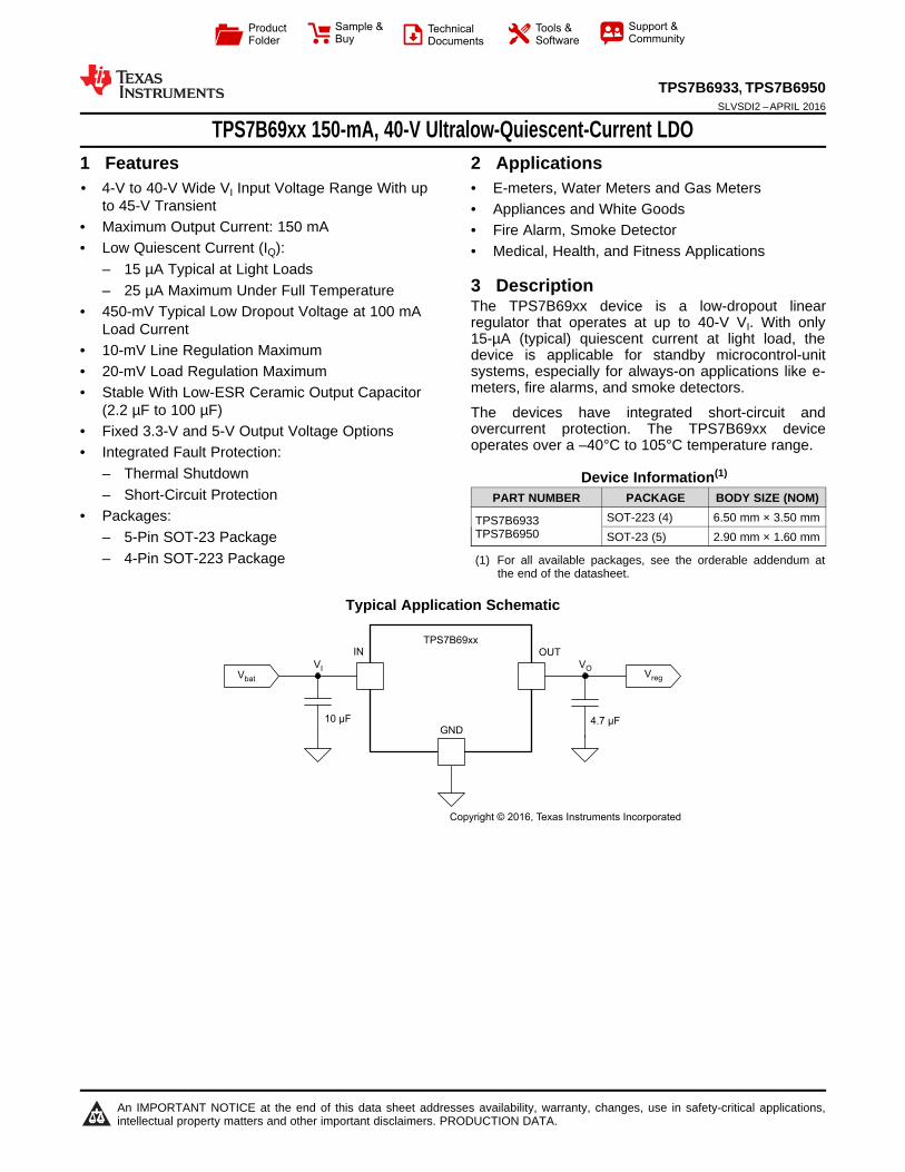
6.5 Electrical CharacteristicsVIN = 14 V, 1 mΩ < ESR < 2 Ω, TJ = –40°C to 125 °C (unless otherwise noted)
PARAMETER TEST CONDITIONS MIN TYP MAX UNITSUPPLY VOLTAGE AND CURRENT (IN)
VI Input voltageFixed 3.3-V output, IO = 1 mA 4 40
VFixed 5-V output, IO = 1 mA 5.5 40
IQ Quiescent current Fixed 3.3-V version, VI = 4 to 40 V, , IO = 0.2 mAFixed 5-V version, VI = 5.5 to 40 V, IO = 0.2 mA 15 25 µA
VIN(UVLO) IN undervoltage detectionRamp VI up until the output turns on 3.65
VRamp VI down until the output turns OFF 3
REGULATED OUTPUT (OUT)
VO Regulated outputFixed 3.3-V version, VI = 5 to 40 V, IO = 1 to 150 mA –3% 3%Fixed 5-V version, VI = 6.5 to 40 V, IO = 1 to 150 mA –3% 3%
ΔVO(ΔVI) Line regulation VI = 6 to 40 V, ∆VO, IO = 10 mA 10 mVΔVO(ΔIL) Load regulation IO = 1 to 150 mA, ∆VO 20 mV
VDROP Dropout voltage
Fixed 3.3-V version, VI – VO, IO = 50 mA 799
mVFixed 3.3-V version, VI – VO, IO = 100 mA 800Fixed 5-V version, VI – VO, IO = 50 mA 220 400Fixed 5-V version, VI – VO, IO = 100 mA 450 800
IO Output current VO in regulation 0 150 mAIOCL Output current-limit OUT short to ground 150 500 mA
PSRR Power supply ripplerejection (1) Vrip = 0.5 Vpp, Load = 10 mA, ƒ = 100 Hz, CO = 2.2 µF 60 dB
OPERATING TEMPERATURE RANGE
TsdJunction shutdowntemperature 175 °C
ThysHysteresis of thermalshutdown 25 °C
6.6 Typical Characteristics
Figure 1. 5-V Output Voltage vs Ambient Temperature
VI = 14 V
Figure 2. 3.3-V Output Voltage vs t Temperature
Output Current (mA)
Dro
pout
Vol
tage
(m
V)
0 20 40 60 80 100 120 140 1600
100
200
300
400
500
600
700
800
900
1000
1100
D004
�40qC25qC105qC
Frequency (Hz)
Pow
er S
uppl
y R
ejec
tion
Rat
io (
dB)
1E+1 1E+2 1E+3 1E+4 1E+5 1E+6 1E+7 5E+70
10
20
30
40
50
60
70
80
D005
Output Current (mA)
Qui
esce
nt C
urre
nt (P
A)
0 30 60 90 120 1500
20
40
60
80
100
120
140
160
D009
�40qC25qC105qC
Supply Voltage (V)
Qui
esce
nt C
urre
nt (P
A)
0 5 10 15 20 25 30 35 400
5
10
15
20
25
30
D010
�40qC25qC105qC
Supply Voltage (V)
Out
put V
olta
ge (
V)
0 5 10 15 20 25 30 35 400
1
2
3
4
5
6
D003Supply Voltage (V)
Out
put V
olta
ge (
V)
0 5 10 15 20 25 30 35 400
0.5
1
1.5
2
2.5
3
3.5
4
D008
6
TPS7B6933, TPS7B6950SLVSDI2 –APRIL 2016 www.ti.com
Product Folder Links: TPS7B6933 TPS7B6950
Submit Documentation Feedback Copyright © 2016, Texas Instruments Incorporated
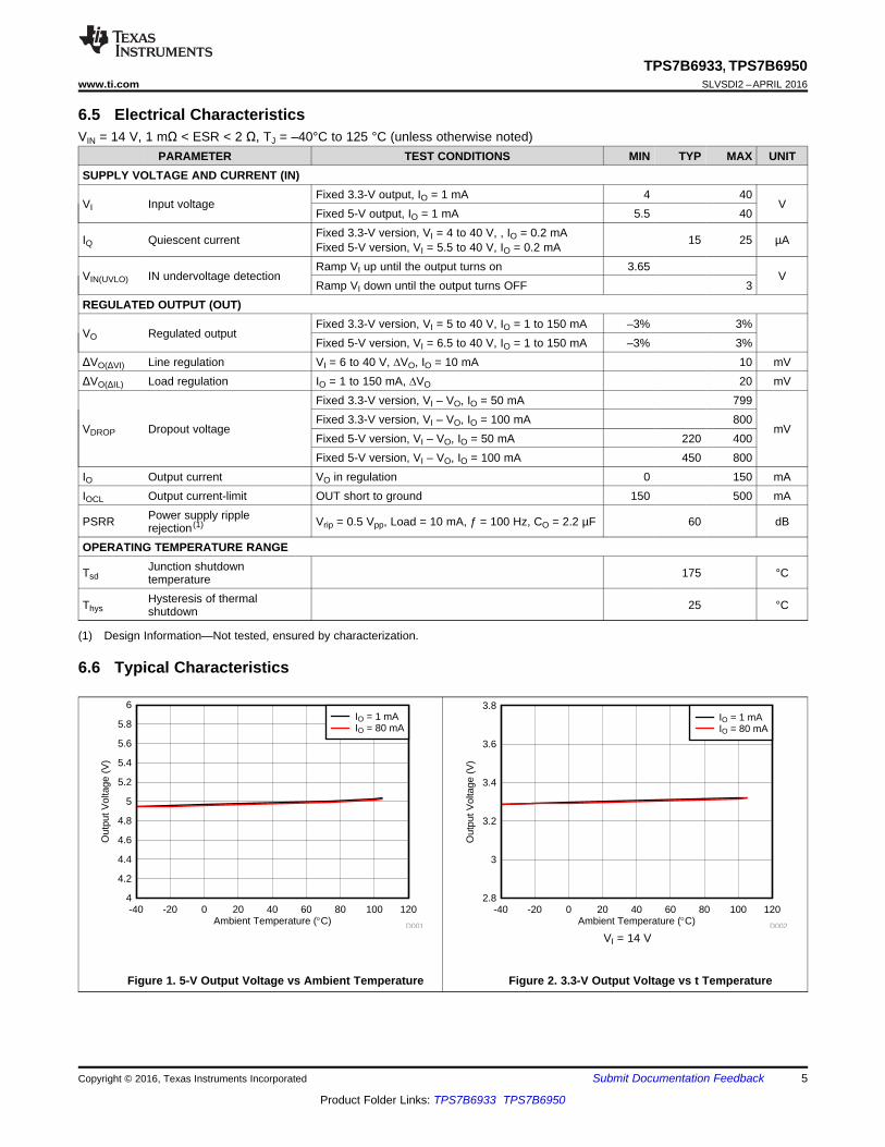
Typical Characteristics (continued)
IO = 0 mA
Figure 3. 5-V Output Voltage vs Supply Voltage
IO = 0 mA
Figure 4. 3.3-V Output Voltage vs Supply Voltage
VI = 14 V
Figure 5. Quiescent Current vs Output Current
IO = 0.2 mA
Figure 6. Quiescent Current vs Supply Voltage
Figure 7. Dropout Voltage vs Output Current
IO = 100 mA VI = 14 V TA = 25°CCO = 2.2 µF
Figure 8. Power Supply Rejection Ratio

I (DC)O
V (AC)O
100 mV/div
50 mA/div
I (DC)O
V (AC)O
100 mV/div
50 mA/div
I (DC)O
V (AC)O
100 mV/div
50 mA/div
I (DC)O
V (AC)O
100 mV/div
50 mA/div
Frequency (Hz)
Pow
er S
uppl
y R
ejec
tion
Rat
io (
dB)
1E+1 1E+2 1E+3 1E+4 1E+5 1E+6 1E+7 5E+70
10
20
30
40
50
60
70
80
90
D006 ESR of Output Capacitance (Ω)
Lo
ad
Cap
acitan
ce
(µ
F)
0.001 0.5 1 1.5 2
2.2
20
40
60
80
100
D007
Stable Region
7
TPS7B6933, TPS7B6950www.ti.com SLVSDI2 –APRIL 2016
Product Folder Links: TPS7B6933 TPS7B6950
Submit Documentation FeedbackCopyright © 2016, Texas Instruments Incorporated
Typical Characteristics (continued)
IO = 10 mA VI = 14 V TA = 25°CCO = 2.2 µF
Figure 9. Power Supply Rejection Ratio Figure 10. ESR Stability vs Output Capacitance
VI = 14 V CO = 2.2 µF 1 ms/divVO = 5 V
Figure 11. Load Transient (1 to 100 mA, 5 V)
VI = 14 V CO = 2.2 µF 1 ms/divVO = 3.3 V
Figure 12. Load Transient (1 to 100 mA, 3.3 V)
VI = 14 V CO = 2.2 µF 1 ms/divVO = 5 V
Figure 13. Load Transient (1 to 150 mA, 5 V)
VI = 14 V CO = 2.2 µF 1 ms/divVO = 3.3 V
Figure 14. Load Transient (1 to 150 mA, 3.3 V)
VI
VO
2 V/div
5 V/div
VI
VO
1 V/div
5 V/div
VI
VO
20 mV/div
5 V/div
VI
VO
20 mV/div
5 V/div
8
TPS7B6933, TPS7B6950SLVSDI2 –APRIL 2016 www.ti.com
Product Folder Links: TPS7B6933 TPS7B6950
Submit Documentation Feedback Copyright © 2016, Texas Instruments Incorporated
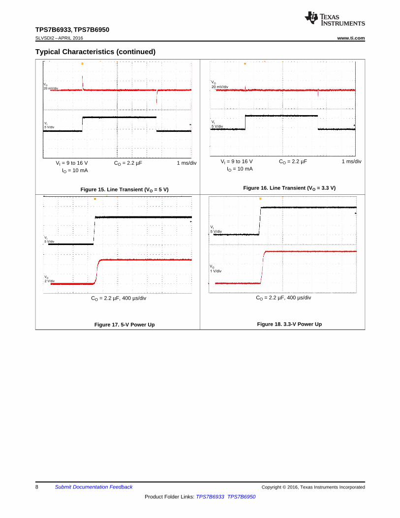
Typical Characteristics (continued)
VI = 9 to 16 V CO = 2.2 µF 1 ms/divIO = 10 mA
Figure 15. Line Transient (VO = 5 V)
VI = 9 to 16 V CO = 2.2 µF 1 ms/divIO = 10 mA
Figure 16. Line Transient (VO = 3.3 V)
CO = 2.2 µF, 400 µs/div
Figure 17. 5-V Power Up
CO = 2.2 µF, 400 µs/div
Figure 18. 3.3-V Power Up
IN
GND
Vref
OUT
+
UVLO
Overcurrent
detection
Regulator
control
Thermal
shutdown
Band gap
Copyright © 2016, Texas Instruments Incorporated
9
TPS7B6933, TPS7B6950www.ti.com SLVSDI2 –APRIL 2016
Product Folder Links: TPS7B6933 TPS7B6950
Submit Documentation FeedbackCopyright © 2016, Texas Instruments Incorporated
7 Detailed Description
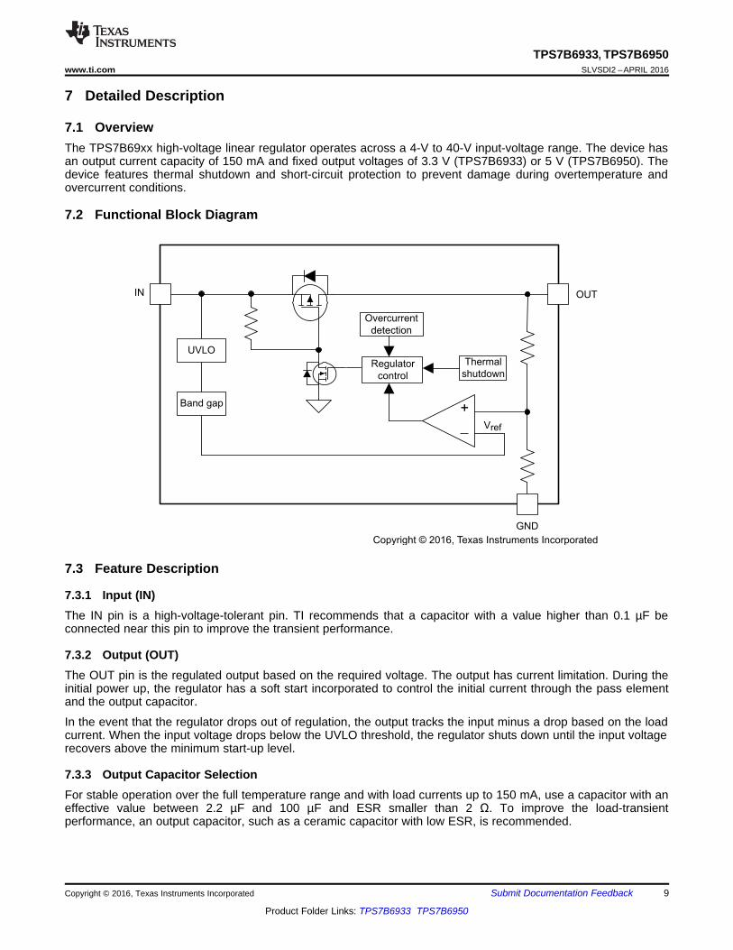
7.1 OverviewThe TPS7B69xx high-voltage linear regulator operates across a 4-V to 40-V input-voltage range. The device hasan output current capacity of 150 mA and fixed output voltages of 3.3 V (TPS7B6933) or 5 V (TPS7B6950). Thedevice features thermal shutdown and short-circuit protection to prevent damage during overtemperature andovercurrent conditions.
7.2 Functional Block Diagram
7.3 Feature Description
7.3.1 Input (IN)The IN pin is a high-voltage-tolerant pin. TI recommends that a capacitor with a value higher than 0.1 µF beconnected near this pin to improve the transient performance.
7.3.2 Output (OUT)The OUT pin is the regulated output based on the required voltage. The output has current limitation. During theinitial power up, the regulator has a soft start incorporated to control the initial current through the pass elementand the output capacitor.
In the event that the regulator drops out of regulation, the output tracks the input minus a drop based on the loadcurrent. When the input voltage drops below the UVLO threshold, the regulator shuts down until the input voltagerecovers above the minimum start-up level.
7.3.3 Output Capacitor SelectionFor stable operation over the full temperature range and with load currents up to 150 mA, use a capacitor with aneffective value between 2.2 µF and 100 µF and ESR smaller than 2 Ω. To improve the load-transientperformance, an output capacitor, such as a ceramic capacitor with low ESR, is recommended.
10
TPS7B6933, TPS7B6950SLVSDI2 –APRIL 2016 www.ti.com
Product Folder Links: TPS7B6933 TPS7B6950
Submit Documentation Feedback Copyright © 2016, Texas Instruments Incorporated
Feature Description (continued)7.3.4 Low-Voltage TrackingAt low input voltages, the regulator drops out of regulation and the output voltage tracks input minus a voltagebased on the load current (IL) and switch resistor. This tracking allows for a smaller input capacitor and canpossibly eliminate the need for a boost converter during cold-crank conditions.
7.3.5 Thermal ShutdownThe TPS7B69xx family of devices incorporates a thermal-shutdown (TSD) circuit as a protection fromoverheating. For continuous normal operation, the junction temperature should not exceed the TSD trip point. Ifthe junction temperature exceeds the TSD trip point, the output turns off. When the junction temperature fallsbelow the TSD trip point minus the hysteresis of TSD, the output turns on again. This cycling limits thedissipation of the regulator, protecting it from damage as a result of overheating.
The purpose of the design of the internal protection circuitry of the TPS7B69xx family of devices is for protectionagainst overload conditions, not as a replacement for proper heat-sinking. Continuously running the TPS7B69xxfamily of devices into thermal shutdown degrades device reliability.
7.4 Device Functional Modes
7.4.1 Operation With VI Less Than 4 VThe TPS7B69xx family of devices operates with input voltages above 4 V. The maximum UVLO voltage is 3 Vand the device operates at an input voltage above 4 V. The device can also operate at lower input voltages; nominimum UVLO voltage is specified. At input voltages below the actual UVLO, the device shuts down.
7.4.2 Operation With VI Greater Than 4 VWhen VI is greater than 4 V, if the input voltage is higher than VO plus the dropout voltage, the output voltage isequal to the set value. Otherwise, the output voltage is equal to VI minus the dropout voltage.
GND10 µF 4.7 µF
VbatVreg
VOVI
IN OUT
Copyright © 2016, Texas Instruments Incorporated
TPS7B69xx
11
TPS7B6933, TPS7B6950www.ti.com SLVSDI2 –APRIL 2016
Product Folder Links: TPS7B6933 TPS7B6950
Submit Documentation FeedbackCopyright © 2016, Texas Instruments Incorporated
8 Application and Implementation
NOTEInformation in the following applications sections is not part of the TI componentspecification, and TI does not warrant its accuracy or completeness. TI’s customers areresponsible for determining suitability of components for their purposes. Customers shouldvalidate and test their design implementation to confirm system functionality.
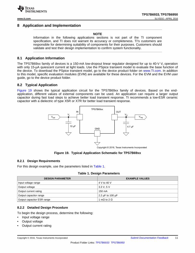
8.1 Application InformationThe TPS7B69xx family of devices is a 150-mA low-dropout linear regulator designed for up to 40-V VI operationwith only 15-µA quiescent current at light loads. Use the PSpice transient model to evaluate the base function ofthe device. To download the PSpice transient model, go to the device product folder on www.TI.com. In additionto this model, specific evaluation modules (EVM) are available for these devices. For the EVM and the EVM userguide, go to the device product folder.
8.2 Typical ApplicationFigure 19 shows the typical application circuit for the TPS7B69xx family of devices. Based on the end-application, different values of external components can be used. An application can require a larger outputcapacitor during fast load steps to achieve better load transient response. TI recommends a low-ESR ceramiccapacitor with a dielectric of type X5R or X7R for better load transient response.
Figure 19. Typical Application Schematic for TPS7B69xx
8.2.1 Design RequirementsFor this design example, use the parameters listed in Table 1.
Table 1. Design ParametersDESIGN PARAMETER EXAMPLE VALUES
Input voltage range 4 V to 40 VOutput voltage 3.3 V, 5 VOutput current rating 150 mAOutput capacitor range 2.2 µF to 100 µFOutput capacitor ESR range 1 mΩ to 2 Ω
8.2.2 Detailed Design ProcedureTo begin the design process, determine the following:• Input voltage range• Output voltage• Output current rating
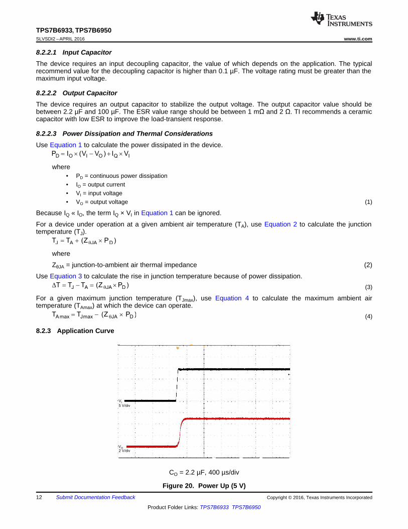
VI
5 V/div
2 V/div
VO
A max Jmax JA DT T (Z P )q
= - ´
J A JA DT T T (Z P )q
D = - = ´
J A JA DT T (Z P )q
= + ´
D O I O Q IP I (V V ) I V= ´ - + ´
12
TPS7B6933, TPS7B6950SLVSDI2 –APRIL 2016 www.ti.com
Product Folder Links: TPS7B6933 TPS7B6950
Submit Documentation Feedback Copyright © 2016, Texas Instruments Incorporated
8.2.2.1 Input CapacitorThe device requires an input decoupling capacitor, the value of which depends on the application. The typicalrecommend value for the decoupling capacitor is higher than 0.1 µF. The voltage rating must be greater than themaximum input voltage.
8.2.2.2 Output CapacitorThe device requires an output capacitor to stabilize the output voltage. The output capacitor value should bebetween 2.2 µF and 100 µF. The ESR value range should be between 1 mΩ and 2 Ω. TI recommends a ceramiccapacitor with low ESR to improve the load-transient response.
8.2.2.3 Power Dissipation and Thermal ConsiderationsUse Equation 1 to calculate the power dissipated in the device.
where• PD = continuous power dissipation• IO = output current• VI = input voltage• VO = output voltage (1)
Because IQ « IO, the term IQ × VI in Equation 1 can be ignored.
For a device under operation at a given ambient air temperature (TA), use Equation 2 to calculate the junctiontemperature (TJ).
where
ZθJA = junction-to-ambient air thermal impedance (2)
Use Equation 3 to calculate the rise in junction temperature because of power dissipation.(3)
For a given maximum junction temperature (TJmax), use Equation 4 to calculate the maximum ambient airtemperature (TAmax) at which the device can operate.
(4)
8.2.3 Application Curve
CO = 2.2 µF, 400 µs/div
Figure 20. Power Up (5 V)

1 2 3
IN GND OUT
GND
4
13
TPS7B6933, TPS7B6950www.ti.com SLVSDI2 –APRIL 2016
Product Folder Links: TPS7B6933 TPS7B6950
Submit Documentation FeedbackCopyright © 2016, Texas Instruments Incorporated
9 Power Supply RecommendationsThe device is designed to operate from an input-voltage supply range between 4 V and 40 V. This input supplymust be well regulated. If the input supply is located more than a few inches from the TPS7B69xx device, TIrecommends adding an electrolytic capacitor with a value of 10 µF and a ceramic bypass capacitor at the input.
10 Layout
10.1 Layout GuidelinesFor the layout of TPS7B69xx family of devices, place the input and output capacitors near the devices as shownin Figure 21 and Figure 22. To enhance the thermal performance, TI recommends surrounding the device withsome vias.
Minimize equivalent series inductance (ESL) and ESR to maximize performance and ensure stability. Placeevery capacitor as close as possible to the device and on the same side of the PCB as the regulator.
Do not place any of the capacitors on the opposite side of the PCB from where the regulator is installed. TIstrongly discourages the use of long traces because they can impact system performance negatively and evencause instability.
If possible, and to ensure the maximum performance specified in this product data sheet, use the same layoutpattern used for the TPS7B69xx evaluation board.
10.2 Layout Example
Figure 21. Layout Example for SOT-223 Package

GND
2
4
1
GND3
5
NC
IN OUT
14
TPS7B6933, TPS7B6950SLVSDI2 –APRIL 2016 www.ti.com
Product Folder Links: TPS7B6933 TPS7B6950
Submit Documentation Feedback Copyright © 2016, Texas Instruments Incorporated
Layout Example (continued)
Figure 22. Layout Example for SOT-23 Package
11 Device and Documentation Support
11.1 Documentation Support
11.1.1 Related DocumentationFor related documentation see the following:
TPS7B6950EVM User's Guide, SLVUAC0.
11.2 Related LinksThe table below lists quick access links. Categories include technical documents, support and communityresources, tools and software, and quick access to sample or buy.
Table 2. Related Links
PARTS PRODUCT FOLDER SAMPLE & BUY TECHNICALDOCUMENTS
TOOLS &SOFTWARE
SUPPORT &COMMUNITY
TPS7B6933 Click here Click here Click here Click here Click hereTPS7B6950 Click here Click here Click here Click here Click here
11.3 TrademarksAll trademarks are the property of their respective owners.
11.4 Electrostatic Discharge CautionThese devices have limited built-in ESD protection. The leads should be shorted together or the device placed in conductive foamduring storage or handling to prevent electrostatic damage to the MOS gates.
11.5 GlossarySLYZ022 — TI Glossary.
This glossary lists and explains terms, acronyms, and definitions.
12 Mechanical, Packaging, and Orderable InformationThe following pages include mechanical, packaging, and orderable information. This information is the most-current data available for the designated devices. This data is subject to change without notice and withoutrevision of this document. For browser-based versions of this data sheet, see the left-hand navigation pane.
PACKAGE OPTION ADDENDUM
www.ti.com 15-Jul-2016
Addendum-Page 1
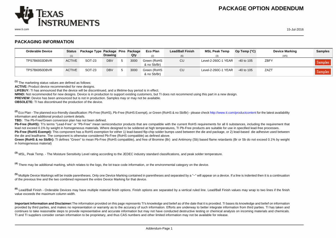
PACKAGING INFORMATION
Orderable Device Status(1)
Package Type PackageDrawing
Pins PackageQty
Eco Plan(2)
Lead/Ball Finish(6)
MSL Peak Temp(3)
Op Temp (°C) Device Marking(4/5)
Samples
TPS7B6933DBVR ACTIVE SOT-23 DBV 5 3000 Green (RoHS& no Sb/Br)
CU Level-2-260C-1 YEAR -40 to 105 ZBFY
TPS7B6950DBVR ACTIVE SOT-23 DBV 5 3000 Green (RoHS& no Sb/Br)
CU Level-2-260C-1 YEAR -40 to 105 ZAZT
(1) The marketing status values are defined as follows:ACTIVE: Product device recommended for new designs.LIFEBUY: TI has announced that the device will be discontinued, and a lifetime-buy period is in effect.NRND: Not recommended for new designs. Device is in production to support existing customers, but TI does not recommend using this part in a new design.PREVIEW: Device has been announced but is not in production. Samples may or may not be available.OBSOLETE: TI has discontinued the production of the device.
(2) Eco Plan - The planned eco-friendly classification: Pb-Free (RoHS), Pb-Free (RoHS Exempt), or Green (RoHS & no Sb/Br) - please check http://www.ti.com/productcontent for the latest availabilityinformation and additional product content details.TBD: The Pb-Free/Green conversion plan has not been defined.Pb-Free (RoHS): TI's terms "Lead-Free" or "Pb-Free" mean semiconductor products that are compatible with the current RoHS requirements for all 6 substances, including the requirement thatlead not exceed 0.1% by weight in homogeneous materials. Where designed to be soldered at high temperatures, TI Pb-Free products are suitable for use in specified lead-free processes.Pb-Free (RoHS Exempt): This component has a RoHS exemption for either 1) lead-based flip-chip solder bumps used between the die and package, or 2) lead-based die adhesive used betweenthe die and leadframe. The component is otherwise considered Pb-Free (RoHS compatible) as defined above.Green (RoHS & no Sb/Br): TI defines "Green" to mean Pb-Free (RoHS compatible), and free of Bromine (Br) and Antimony (Sb) based flame retardants (Br or Sb do not exceed 0.1% by weightin homogeneous material)
(3) MSL, Peak Temp. - The Moisture Sensitivity Level rating according to the JEDEC industry standard classifications, and peak solder temperature.
(4) There may be additional marking, which relates to the logo, the lot trace code information, or the environmental category on the device.
(5) Multiple Device Markings will be inside parentheses. Only one Device Marking contained in parentheses and separated by a "~" will appear on a device. If a line is indented then it is a continuationof the previous line and the two combined represent the entire Device Marking for that device.
(6) Lead/Ball Finish - Orderable Devices may have multiple material finish options. Finish options are separated by a vertical ruled line. Lead/Ball Finish values may wrap to two lines if the finishvalue exceeds the maximum column width.
Important Information and Disclaimer:The information provided on this page represents TI's knowledge and belief as of the date that it is provided. TI bases its knowledge and belief on informationprovided by third parties, and makes no representation or warranty as to the accuracy of such information. Efforts are underway to better integrate information from third parties. TI has taken andcontinues to take reasonable steps to provide representative and accurate information but may not have conducted destructive testing or chemical analysis on incoming materials and chemicals.TI and TI suppliers consider certain information to be proprietary, and thus CAS numbers and other limited information may not be available for release.
PACKAGE OPTION ADDENDUM
www.ti.com 15-Jul-2016
Addendum-Page 2
In no event shall TI's liability arising out of such information exceed the total purchase price of the TI part(s) at issue in this document sold by TI to Customer on an annual basis.
OTHER QUALIFIED VERSIONS OF TPS7B6933, TPS7B6950 :
• Automotive: TPS7B6933-Q1, TPS7B6950-Q1
NOTE: Qualified Version Definitions:
• Automotive - Q100 devices qualified for high-reliability automotive applications targeting zero defects
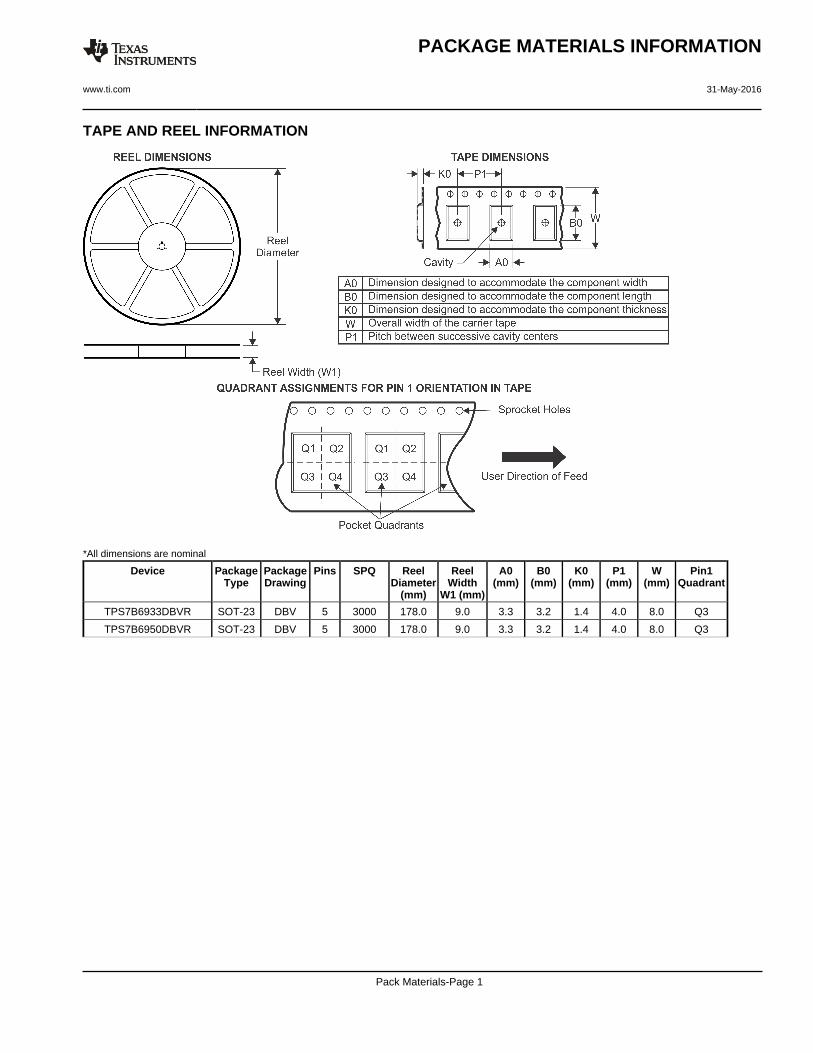
TAPE AND REEL INFORMATION
*All dimensions are nominal
Device PackageType
PackageDrawing
Pins SPQ ReelDiameter
(mm)
ReelWidth
W1 (mm)
A0(mm)
B0(mm)
K0(mm)
P1(mm)
W(mm)
Pin1Quadrant
TPS7B6933DBVR SOT-23 DBV 5 3000 178.0 9.0 3.3 3.2 1.4 4.0 8.0 Q3
TPS7B6950DBVR SOT-23 DBV 5 3000 178.0 9.0 3.3 3.2 1.4 4.0 8.0 Q3
PACKAGE MATERIALS INFORMATION
www.ti.com 31-May-2016
Pack Materials-Page 1
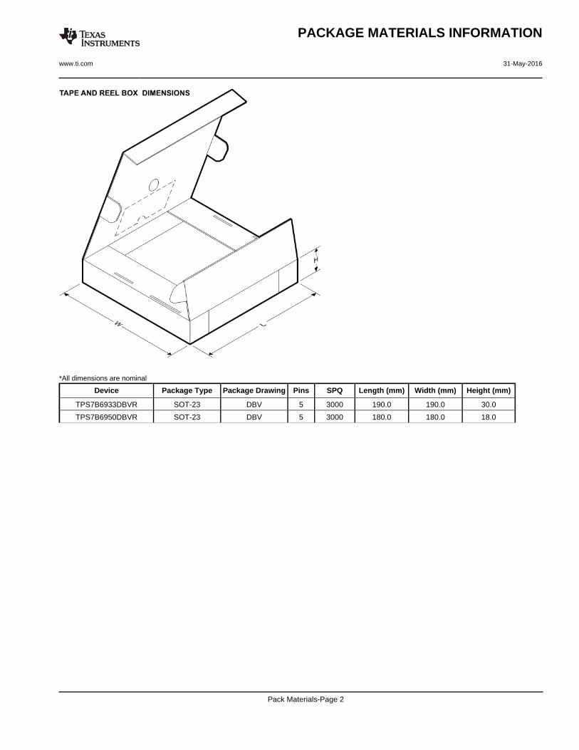
*All dimensions are nominal
Device Package Type Package Drawing Pins SPQ Length (mm) Width (mm) Height (mm)
TPS7B6933DBVR SOT-23 DBV 5 3000 190.0 190.0 30.0
TPS7B6950DBVR SOT-23 DBV 5 3000 180.0 180.0 18.0
PACKAGE MATERIALS INFORMATION
www.ti.com 31-May-2016
Pack Materials-Page 2
IMPORTANT NOTICE
Texas Instruments Incorporated and its subsidiaries (TI) reserve the right to make corrections, enhancements, improvements and otherchanges to its semiconductor products and services per JESD46, latest issue, and to discontinue any product or service per JESD48, latestissue. Buyers should obtain the latest relevant information before placing orders and should verify that such information is current andcomplete. All semiconductor products (also referred to herein as “components”) are sold subject to TI’s terms and conditions of salesupplied at the time of order acknowledgment.TI warrants performance of its components to the specifications applicable at the time of sale, in accordance with the warranty in TI’s termsand conditions of sale of semiconductor products. Testing and other quality control techniques are used to the extent TI deems necessaryto support this warranty. Except where mandated by applicable law, testing of all parameters of each component is not necessarilyperformed.TI assumes no liability for applications assistance or the design of Buyers’ products. Buyers are responsible for their products andapplications using TI components. To minimize the risks associated with Buyers’ products and applications, Buyers should provideadequate design and operating safeguards.TI does not warrant or represent that any license, either express or implied, is granted under any patent right, copyright, mask work right, orother intellectual property right relating to any combination, machine, or process in which TI components or services are used. Informationpublished by TI regarding third-party products or services does not constitute a license to use such products or services or a warranty orendorsement thereof. Use of such information may require a license from a third party under the patents or other intellectual property of thethird party, or a license from TI under the patents or other intellectual property of TI.Reproduction of significant portions of TI information in TI data books or data sheets is permissible only if reproduction is without alterationand is accompanied by all associated warranties, conditions, limitations, and notices. TI is not responsible or liable for such altereddocumentation. Information of third parties may be subject to additional restrictions.Resale of TI components or services with statements different from or beyond the parameters stated by TI for that component or servicevoids all express and any implied warranties for the associated TI component or service and is an unfair and deceptive business practice.TI is not responsible or liable for any such statements.Buyer acknowledges and agrees that it is solely responsible for compliance with all legal, regulatory and safety-related requirementsconcerning its products, and any use of TI components in its applications, notwithstanding any applications-related information or supportthat may be provided by TI. Buyer represents and agrees that it has all the necessary expertise to create and implement safeguards whichanticipate dangerous consequences of failures, monitor failures and their consequences, lessen the likelihood of failures that might causeharm and take appropriate remedial actions. Buyer will fully indemnify TI and its representatives against any damages arising out of the useof any TI components in safety-critical applications.In some cases, TI components may be promoted specifically to facilitate safety-related applications. With such components, TI’s goal is tohelp enable customers to design and create their own end-product solutions that meet applicable functional safety standards andrequirements. Nonetheless, such components are subject to these terms.No TI components are authorized for use in FDA Class III (or similar life-critical medical equipment) unless authorized officers of the partieshave executed a special agreement specifically governing such use.Only those TI components which TI has specifically designated as military grade or “enhanced plastic” are designed and intended for use inmilitary/aerospace applications or environments. Buyer acknowledges and agrees that any military or aerospace use of TI componentswhich have not been so designated is solely at the Buyer's risk, and that Buyer is solely responsible for compliance with all legal andregulatory requirements in connection with such use.TI has specifically designated certain components as meeting ISO/TS16949 requirements, mainly for automotive use. In any case of use ofnon-designated products, TI will not be responsible for any failure to meet ISO/TS16949.
Products ApplicationsAudio www.ti.com/audio Automotive and Transportation www.ti.com/automotiveAmplifiers amplifier.ti.com Communications and Telecom www.ti.com/communicationsData Converters dataconverter.ti.com Computers and Peripherals www.ti.com/computersDLP® Products www.dlp.com Consumer Electronics www.ti.com/consumer-appsDSP dsp.ti.com Energy and Lighting www.ti.com/energyClocks and Timers www.ti.com/clocks Industrial www.ti.com/industrialInterface interface.ti.com Medical www.ti.com/medicalLogic logic.ti.com Security www.ti.com/securityPower Mgmt power.ti.com Space, Avionics and Defense www.ti.com/space-avionics-defenseMicrocontrollers microcontroller.ti.com Video and Imaging www.ti.com/videoRFID www.ti-rfid.comOMAP Applications Processors www.ti.com/omap TI E2E Community e2e.ti.comWireless Connectivity www.ti.com/wirelessconnectivity
Mailing Address: Texas Instruments, Post Office Box 655303, Dallas, Texas 75265Copyright © 2016, Texas Instruments Incorporated