TPS74201 Datasheet - Texas Instruments · 1V/div 1V/div Time (1ms/div) C = 0 FSS m C = 0.001 FSS m...
36
1V/div 1V/div Time (1ms/div) C = 0 F SS m C = 0.001 F SS m C = 0.0047 F SS m V OUT V EN 0V 1.2V TPS74201 GND EN FB IN PG BIAS SS OUT V IN V OUT R 1 R 2 R 3 C OUT Optional C IN 1μF C SS V BIAS C BIAS 1μF Product Folder Order Now Technical Documents Tools & Software Support & Community An IMPORTANT NOTICE at the end of this data sheet addresses availability, warranty, changes, use in safety-critical applications, intellectual property matters and other important disclaimers. PRODUCTION DATA. TPS74201 SBVS064N – DECEMBER 2005 – REVISED NOVEMBER 2016 TPS742 1.5-A Ultra-LDO With Programmable Soft-Start 1 1 Features 1• Input Voltage Range: 0.8 V to 5.5 V • Soft-Start (SS) Pin Provides a Linear Start-Up With Ramp Time Set by External Capacitor • 1% Accuracy Over Line, Load, and Temperature • Supports Input Voltages as Low as 0.8 V With External Bias Supply • Adjustable Output (0.8 V to 3.6 V) • Ultra-Low Dropout: 55 mV at 1.5 A (Typical) • Stable With Any or No Output Capacitor • Excellent Transient Response • Open-Drain Power-Good (VQFN) • Active High Enable 2 Applications • FPGA Applications • DSP Core and I/O Voltages • Servers • Post-Regulation Applications • Applications With Special Start-Up Time or Sequencing Requirements 3 Description The TPS742 series of low-dropout (LDO) linear regulators provide an easy-to-use, robust power- management solution for a wide variety of applications. User-programmable soft-start minimizes stress on the input power source by reducing capacitive inrush current on start-up. The soft-start is monotonic and well suited for powering many different types of processors and ASICs. The enable input and power-good output allow easy sequencing with external regulators. This complete flexibility permits the user to configure a solution that meets the sequencing requirements of FPGAs, DSPs, and other applications with special start-up requirements. A precision reference and error amplifier deliver 1% accuracy over load, line, temperature, and process. Each LDO is stable with low-cost ceramic output capacitors, and the family is fully specified from –40°C to 125°C. The TPS742 devices are offered in a small 5-mm × 5-mm VQFN (RGW) and a small 3.5-mm × 3.5-mm VQFN (RGR) package, yielding a highly compact total solution size. For applications that require additional power dissipation, the DDPAK/TO-263 (KTW) package is also available. Device Information (1) PART NUMBER PACKAGE BODY SIZE (NOM) TPS74201 VQFN (20), RGW 5.00 mm × 5.00 mm VQFN (20), RGR 3.50 mm × 3.50 mm DDPAK/TO-263 (7) 8.89 mm × 10.10 mm (1) For all available packages, see the orderable addendum at the end of the data sheet. Typical Application Adjustable Output Version Turnon Response
Transcript of TPS74201 Datasheet - Texas Instruments · 1V/div 1V/div Time (1ms/div) C = 0 FSS m C = 0.001 FSS m...

1V/div
1V/div
Time (1ms/div)
C = 0 FSS m
C = 0.001 FSS m
C = 0.0047 FSS m
VOUT
VEN
0V
1.2V
TPS74201
GND
EN
FB
IN PG
BIAS
SS
OUT
VIN
VOUT
R1
R2
R3
COUT
Optional
CIN
1µF
CSS
VBIAS
CBIAS
1µF
Product
Folder
Order
Now
Technical
Documents
Tools &
Software
Support &Community
An IMPORTANT NOTICE at the end of this data sheet addresses availability, warranty, changes, use in safety-critical applications,intellectual property matters and other important disclaimers. PRODUCTION DATA.
TPS74201SBVS064N –DECEMBER 2005–REVISED NOVEMBER 2016
TPS7421.5-A Ultra-LDO With Programmable Soft-Start
1
1 Features1• Input Voltage Range: 0.8 V to 5.5 V• Soft-Start (SS) Pin Provides a Linear Start-Up
With Ramp Time Set by External Capacitor• 1% Accuracy Over Line, Load, and Temperature• Supports Input Voltages as Low as 0.8 V With
External Bias Supply• Adjustable Output (0.8 V to 3.6 V)• Ultra-Low Dropout: 55 mV at 1.5 A (Typical)• Stable With Any or No Output Capacitor• Excellent Transient Response• Open-Drain Power-Good (VQFN)• Active High Enable
2 Applications• FPGA Applications• DSP Core and I/O Voltages• Servers• Post-Regulation Applications• Applications With Special Start-Up Time or
Sequencing Requirements
3 DescriptionThe TPS742 series of low-dropout (LDO) linearregulators provide an easy-to-use, robust power-management solution for a wide variety ofapplications. User-programmable soft-start minimizesstress on the input power source by reducingcapacitive inrush current on start-up. The soft-start ismonotonic and well suited for powering manydifferent types of processors and ASICs. The enableinput and power-good output allow easy sequencingwith external regulators. This complete flexibilitypermits the user to configure a solution that meetsthe sequencing requirements of FPGAs, DSPs, andother applications with special start-up requirements.
A precision reference and error amplifier deliver 1%accuracy over load, line, temperature, and process.Each LDO is stable with low-cost ceramic outputcapacitors, and the family is fully specified from–40°C to 125°C. The TPS742 devices are offered ina small 5-mm × 5-mm VQFN (RGW) and a small3.5-mm × 3.5-mm VQFN (RGR) package, yielding ahighly compact total solution size. For applicationsthat require additional power dissipation, theDDPAK/TO-263 (KTW) package is also available.
Device Information(1)
PARTNUMBER PACKAGE BODY SIZE (NOM)
TPS74201VQFN (20), RGW 5.00 mm × 5.00 mmVQFN (20), RGR 3.50 mm × 3.50 mmDDPAK/TO-263 (7) 8.89 mm × 10.10 mm
(1) For all available packages, see the orderable addendum atthe end of the data sheet.
Typical Application Adjustable Output Version Turnon Response

2
TPS74201SBVS064N –DECEMBER 2005–REVISED NOVEMBER 2016 www.ti.com
Product Folder Links: TPS74201
Submit Documentation Feedback Copyright © 2005–2016, Texas Instruments Incorporated
Table of Contents1 Features .................................................................. 12 Applications ........................................................... 13 Description ............................................................. 14 Revision History..................................................... 25 Pin Configuration and Functions ......................... 46 Specifications......................................................... 5
6.1 Absolute Maximum Ratings ..................................... 56.2 ESD Ratings ............................................................ 56.3 Recommended Operating Conditions....................... 56.4 Thermal Information .................................................. 66.5 Electrical Characteristics........................................... 76.6 Typical Characteristics .............................................. 8
7 Detailed Description ............................................ 127.1 Overview ................................................................. 127.2 Functional Block Diagram ....................................... 127.3 Feature Description................................................. 137.4 Device Functional Modes........................................ 13
8 Application and Implementation ........................ 15
8.1 Application Information............................................ 158.2 Typical Applications ................................................ 19
9 Power Supply Recommendations ...................... 2010 Layout................................................................... 21
10.1 Layout Guidelines ................................................. 2110.2 Layout Example .................................................... 2110.3 Thermal Protection................................................ 2210.4 Thermal Considerations ........................................ 22
11 Device and Documentation Support ................. 2511.1 Device Support...................................................... 2511.2 Documentation Support ....................................... 2511.3 Receiving Notification of Documentation Updates 2511.4 Community Resources.......................................... 2511.5 Trademarks ........................................................... 2511.6 Electrostatic Discharge Caution............................ 2511.7 Glossary ................................................................ 25
12 Mechanical, Packaging, and OrderableInformation ........................................................... 26
4 Revision HistoryNOTE: Page numbers for previous revisions may differ from page numbers in the current version.
Changes from Revision M (October 2015) to Revision N Page
• Added RGR package to document ........................................................................................................................................ 1• Deleted Packages Features bullet ......................................................................................................................................... 1• Changed Power-Good Features bullet ................................................................................................................................... 1• Added RGR package to last paragraph of Description section ............................................................................................. 1• Added RGR row to Device Information table ........................................................................................................................ 1• Added RGR package to Pin Configuration and Functions section ........................................................................................ 4• Changed pinout view of KTW package to Top View .............................................................................................................. 4• Added RGR package to Thermal Information table .............................................................................................................. 6• Changed Figure 32 title to reflect both VQFN packages instead of just one ....................................................................... 21
Changes from Revision L (November 2010) to Revision M Page
• Added ESD Ratings table, Feature Description section, Device Functional Modes, Application and Implementationsection, Power Supply Recommendations section, Layout section, Device and Documentation Support section, andMechanical, Packaging, and Orderable Information section .................................................................................................. 1
• Updated the value in Normal and Dropout modes under VBIAS column ............................................................................... 14
Changes from Revision K (August, 2010) to Revision L Page
• Replaced the Dissipation Ratings table with the Thermal Information table .......................................................................... 6• Corrected equation for Table 2............................................................................................................................................. 17• Revised Layout Recommendations and Power Dissipation section .................................................................................... 21

3
TPS74201www.ti.com SBVS064N –DECEMBER 2005–REVISED NOVEMBER 2016
Product Folder Links: TPS74201
Submit Documentation FeedbackCopyright © 2005–2016, Texas Instruments Incorporated
Changes from Revision J (December, 2009) to Revision K Page
• Revised Layout Guidelines section ...................................................................................................................................... 21• Changed final paragraph of Layout Guidelines section........................................................................................................ 21• Revised Estimating Junction Temperature section .............................................................................................................. 22

IN
IN
IN
PG
BIAS
OUT
OUT
OUT
NC
FB/SNS
TPS742xx
INE
N11
GN
D12
NC
13
NC
14
SS
15
6
7
8
9
10
20
19
18
17
16
5
NC
4
NC
3
NC
2
OU
T1
GND
OUT
GND BIAS
IN
FB/
SNS
SS
1 2 3 4 5 6
EN
7
4
TPS74201SBVS064N –DECEMBER 2005–REVISED NOVEMBER 2016 www.ti.com
Product Folder Links: TPS74201
Submit Documentation Feedback Copyright © 2005–2016, Texas Instruments Incorporated
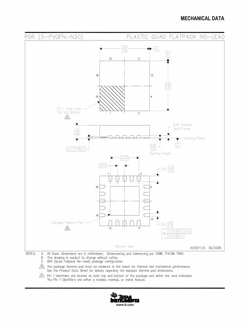
5 Pin Configuration and Functions
RGW, RGR Packages20-Pin VQFN with Exposed Thermal Pad
Top View
KTW Package7-Pin DDPAK/TO-263
Top View
Pin FunctionsPIN
I/O DESCRIPTIONNAME
KTW(DDPAK/TO-263)
RGW, RGR(VQFN)
BIAS 6 10 I Bias input voltage for error amplifier, reference, and internal control circuits.
EN 7 11 I Enable pin. Driving this pin high enables the regulator. Driving this pin low putsthe regulator into shutdown mode. This pin must not be left floating.
FB 2 16 IThis pin is the feedback connection to the center tap of an external resistordivider network that sets the output voltage. This pin must not be left floating.(Adjustable version only.)
GND 4 12 — GroundIN 5 5,6,7,8 I Unregulated input to the device.
NC — 2, 3,4,13,14,17 O No connection. This pin can be left floating or connected to GND to allow better
thermal contact to the top-side plane.OUT 3 1, 18, 19, 20 O Regulated output voltage. No capacitor is required on this pin for stability.PAD/TAB — — — Solder to the ground plane for increased thermal performance.
PG — 9 O
Power-Good (PG) is an open-drain, active-high output that indicates the statusof VOUT. When VOUT exceeds the PG trip threshold, the PG pin goes into ahigh-impedance state. When VOUT is below this threshold the pin is driven to alow-impedance state. Connect a pullup resistor from 10 kΩ to 1 MΩ from thispin to a supply up to 5.5 V. The supply can be higher than the input voltage.Alternatively, the PG pin can be left floating if output monitoring is notnecessary.
SNS 2 16 I This pin is the sense connection to the load device. This pin must beconnected to VOUT and must not be left floating. (Fixed versions only.)
SS 1 15 —Soft-Start pin. A capacitor connected on this pin to ground sets the start-uptime. If this pin is left floating, the regulator output soft-start ramp time istypically 100 μs.
5
TPS74201www.ti.com SBVS064N –DECEMBER 2005–REVISED NOVEMBER 2016
Product Folder Links: TPS74201
Submit Documentation FeedbackCopyright © 2005–2016, Texas Instruments Incorporated
(1) Stresses beyond those listed under Absolute Maximum Ratings may cause permanent damage to the device. These are stress ratingsonly, which do not imply functional operation of the device at these or any other conditions beyond those indicated under RecommendedOperating Conditions. Exposure to absolute-maximum-rated conditions for extended periods may affect device reliability.
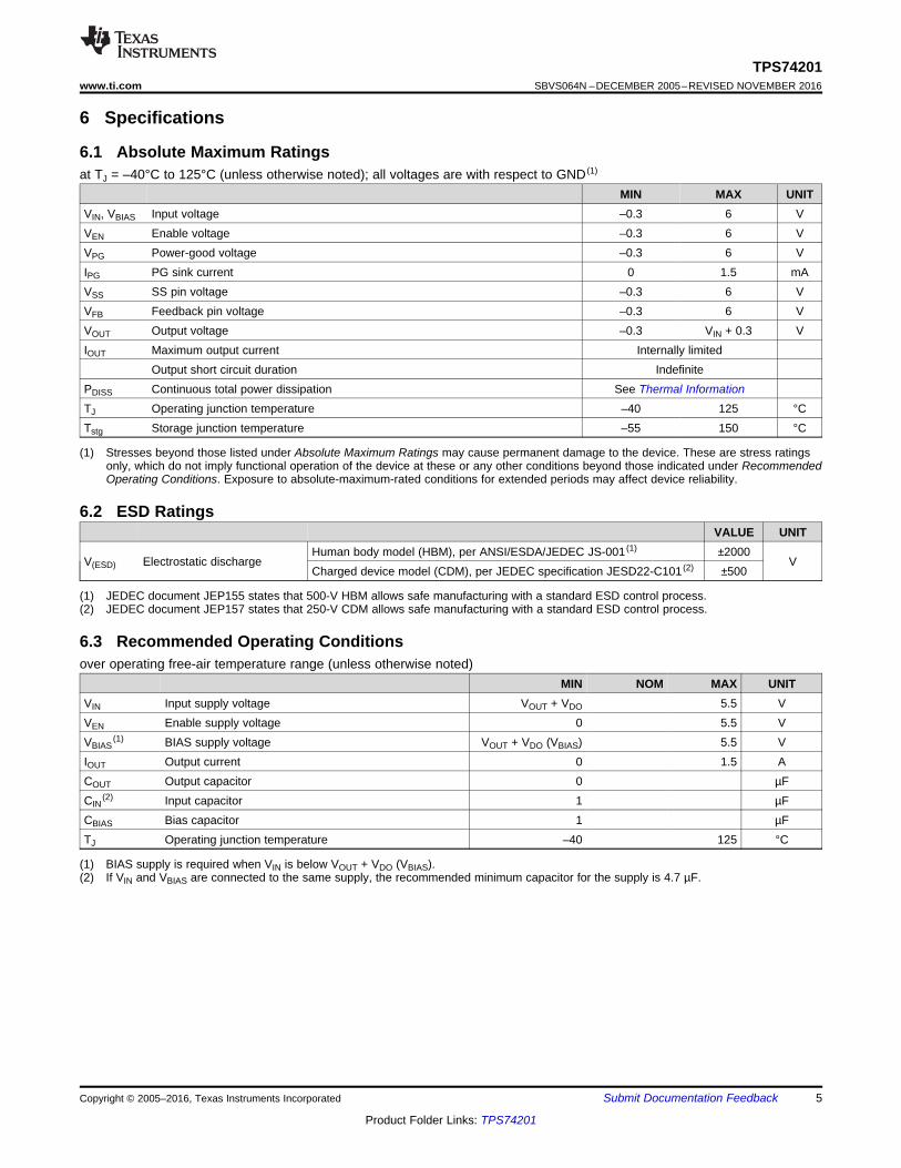
6 Specifications
6.1 Absolute Maximum Ratingsat TJ = –40°C to 125°C (unless otherwise noted); all voltages are with respect to GND (1)
MIN MAX UNITVIN, VBIAS Input voltage –0.3 6 VVEN Enable voltage –0.3 6 VVPG Power-good voltage –0.3 6 VIPG PG sink current 0 1.5 mAVSS SS pin voltage –0.3 6 VVFB Feedback pin voltage –0.3 6 VVOUT Output voltage –0.3 VIN + 0.3 VIOUT Maximum output current Internally limited
Output short circuit duration IndefinitePDISS Continuous total power dissipation See Thermal InformationTJ Operating junction temperature –40 125 °CTstg Storage junction temperature –55 150 °C
(1) JEDEC document JEP155 states that 500-V HBM allows safe manufacturing with a standard ESD control process.(2) JEDEC document JEP157 states that 250-V CDM allows safe manufacturing with a standard ESD control process.
6.2 ESD RatingsVALUE UNIT
V(ESD) Electrostatic dischargeHuman body model (HBM), per ANSI/ESDA/JEDEC JS-001 (1) ±2000
VCharged device model (CDM), per JEDEC specification JESD22-C101 (2) ±500
(1) BIAS supply is required when VIN is below VOUT + VDO (VBIAS).(2) If VIN and VBIAS are connected to the same supply, the recommended minimum capacitor for the supply is 4.7 µF.
6.3 Recommended Operating Conditionsover operating free-air temperature range (unless otherwise noted)
MIN NOM MAX UNITVIN Input supply voltage VOUT + VDO 5.5 VVEN Enable supply voltage 0 5.5 VVBIAS
(1) BIAS supply voltage VOUT + VDO (VBIAS) 5.5 VIOUT Output current 0 1.5 ACOUT Output capacitor 0 µFCIN
(2) Input capacitor 1 µFCBIAS Bias capacitor 1 µFTJ Operating junction temperature –40 125 °C
6
TPS74201SBVS064N –DECEMBER 2005–REVISED NOVEMBER 2016 www.ti.com
Product Folder Links: TPS74201
Submit Documentation Feedback Copyright © 2005–2016, Texas Instruments Incorporated
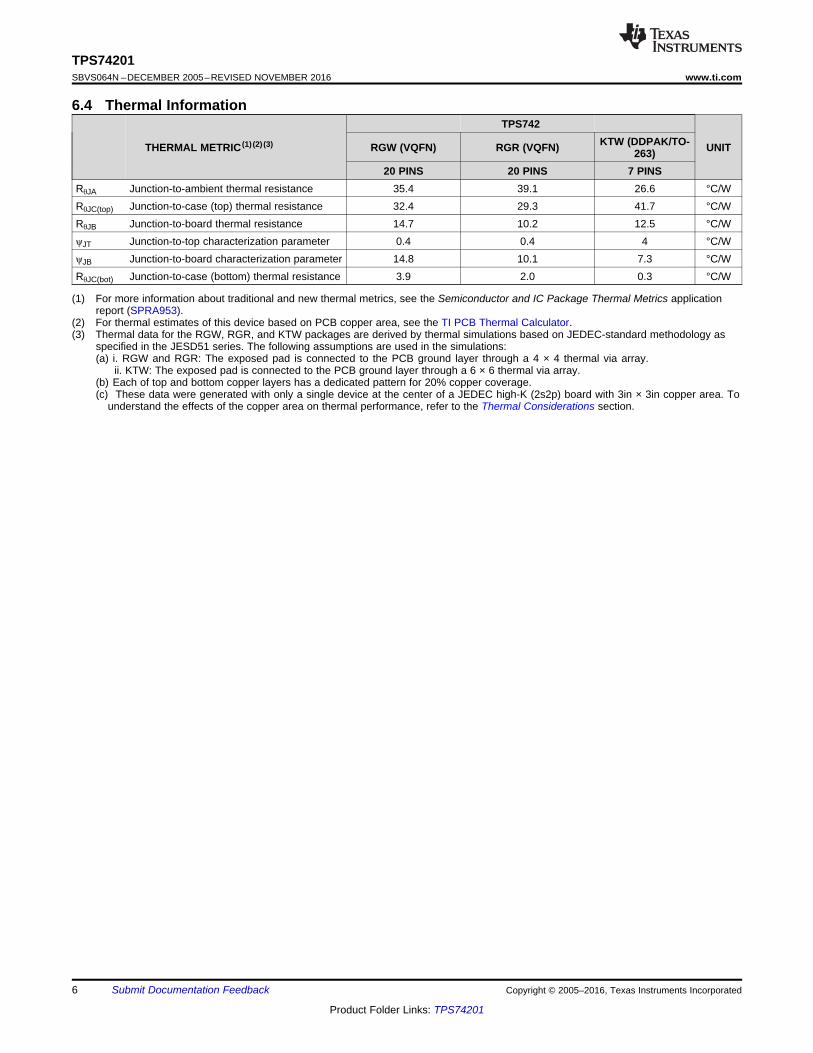
(1) For more information about traditional and new thermal metrics, see the Semiconductor and IC Package Thermal Metrics applicationreport (SPRA953).
(2) For thermal estimates of this device based on PCB copper area, see the TI PCB Thermal Calculator.(3) Thermal data for the RGW, RGR, and KTW packages are derived by thermal simulations based on JEDEC-standard methodology as
specified in the JESD51 series. The following assumptions are used in the simulations:(a) i. RGW and RGR: The exposed pad is connected to the PCB ground layer through a 4 × 4 thermal via array.
- ii. KTW: The exposed pad is connected to the PCB ground layer through a 6 × 6 thermal via array.(b) Each of top and bottom copper layers has a dedicated pattern for 20% copper coverage.(c) These data were generated with only a single device at the center of a JEDEC high-K (2s2p) board with 3in × 3in copper area. To
understand the effects of the copper area on thermal performance, refer to the Thermal Considerations section.
6.4 Thermal Information
THERMAL METRIC (1) (2) (3)
TPS742
UNITRGW (VQFN) RGR (VQFN) KTW (DDPAK/TO-263)
20 PINS 20 PINS 7 PINSRθJA Junction-to-ambient thermal resistance 35.4 39.1 26.6 °C/WRθJC(top) Junction-to-case (top) thermal resistance 32.4 29.3 41.7 °C/WRθJB Junction-to-board thermal resistance 14.7 10.2 12.5 °C/WψJT Junction-to-top characterization parameter 0.4 0.4 4 °C/WψJB Junction-to-board characterization parameter 14.8 10.1 7.3 °C/WRθJC(bot) Junction-to-case (bottom) thermal resistance 3.9 2.0 0.3 °C/W

7
TPS74201www.ti.com SBVS064N –DECEMBER 2005–REVISED NOVEMBER 2016
Product Folder Links: TPS74201
Submit Documentation FeedbackCopyright © 2005–2016, Texas Instruments Incorporated
(1) Adjustable devices tested at 0.8V; resistor tolerance is not taken into account.(2) Dropout is defined as the voltage from the input to VOUT when VOUT is 2% below nominal.(3) IFB, ISNS current flow is out of the device.
6.5 Electrical Characteristicsat VEN = 1.1 V, VIN = VOUT + 0.3 V, CIN = CBIAS = 0.1 μF, COUT = 10 μF, IOUT = 50 mA, VBIAS = 5 V, and TJ = –40°C to 125°C(unless otherwise noted); typical values are at TJ = 25°C
PARAMETER TEST CONDITIONS MIN TYP MAX UNIT
VIN Input voltage VOUT + VDO 5.5 V
VBIAS Bias pin voltage 2.375 5.25 V
VREF Internal reference (adjustable) TJ = 25°C 0.796 0.8 0.804 V
VOUT
Output voltage VIN = 5 V, IOUT = 1.5 A, VBIAS = 5 V VREF 3.6 V
Accuracy (1) 2.375 V ≤ VBIAS ≤ 5.25 V, VOUT + 1.62 V ≤ VBIAS50 mA ≤ IOUT ≤ 1.5 A –1% ±0.2% 1%
VOUT/VIN Line regulationVOUT (NOM) + 0.3 ≤ VIN ≤ 5.5 V, VQFN 0.0005 0.05
%/VVOUT (NOM) + 0.3 ≤ VIN ≤ 5.5 V, DDPAK/TO-263 0.0005 0.06
VOUT/IOUT Load regulation0 mA ≤ IOUT ≤ 50 mA 0.013 %/mA
50 mA ≤ IOUT ≤ 1.5 A 0.04 %/A
VDOVIN dropout voltage (2)
IOUT = 1.5 A, VBIAS – VOUT (NOM) ≥ 1.62 V, VQFN 55 100mVIOUT = 1.5 A, VBIAS – VOUT (NOM) ≥ 1.62 V,
DDPAK/TO-263 60 120
VBIAS dropout voltage (2) IOUT = 1.5 A, VIN = VBIAS 1.4 V
ICL Current limit VOUT = 80% × VOUT (NOM) 1.8 4 A
IBIAS Bias pin current IOUT = 0 mA to 1.5 A 2 4 mA
ISHDN Shutdown supply current (VIN) VEN ≤ 0.4 V 1 100 μA
IFB, ISNSFeedback, Sense pincurrent (3) IOUT = 50 mA to 1.5 A –250 68 250 nA
PSRR
Power-supply rejection(VIN to VOUT)
1 kHz, IOUT = 1.5 A, VIN = 1.8 V, VOUT = 1.5 V 73dB
300 kHz, IOUT = 1.5 A, VIN = 1.8 V, VOUT = 1.5 V 42
Power-supply rejection(VBIAS to VOUT)
1 kHz, IOUT = 1.5 A, VIN = 1.8 V, VOUT = 1.5 V 62dB
300 kHz, IOUT = 1.5 A, VIN = 1.8 V, VOUT = 1.5 V 50
Noise Output noise voltage 100 Hz to 100 kHz, IOUT = 1.5 A, CSS = 0.001 μF 16 × VOUT μVRMS
VTRAN%VOUT droop during loadtransient IOUT = 50 mA to 1.5 A at 1 A/μs, COUT = none 3.5 %VOUT
tSTR Minimum start-up time IOUT = 1.5 A, CSS = open 100 μs
ISS Soft-start charging current VSS = 0.4 V 0.5 0.73 1 μA
VEN, HI Enable input high level 1.1 5.5 V
VEN, LO Enable input low level 0 0.4 V
VEN, HYS Enable pin hysteresis 50 mV
VEN, DG Enable pin deglitch time 20 μs
IEN Enable pin current VEN = 5 V 0.1 1 μA
VIT PG trip threshold VOUT decreasing 86.5 90 93.5 %VOUT
VHYS PG trip hysteresis 3 %VOUT
VPG, LO PG output low voltage IPG = 1 mA (sinking), VOUT < VIT 0.3 V
IPG, LKG PG leakage current VPG = 5.25 V, VOUT > VIT 0.03 1 μA
TJOperating junctiontemperature –40 125 °C
TSDThermal shutdowntemperature
Shutdown, temperature increasing 155°C
Reset, temperature decreasing 140

200
180
160
140
120
100
80
60
40
20
0
0.9 1.4 1.9 2.4 2.9 3.4
Dro
po
ut
Vo
lta
ge
(m
V)
V V-BIAS OUT (V)
3.9
+125 C°
+25 C°
-40°C
I = 1.5AOUT
60
50
40
30
20
10
0
0.9 1.4 1.9 2.4 2.9 3.4
Dro
po
ut
Vo
lta
ge
(m
V)
V -BIAS VOUT (V)
3.9
+125 C°
+25 C°
-40°C
I = 500mAOUT
0.05
0.04
0.03
0.02
0.01
0
-0.01
-0.02
-0.03
-0.04
-0.050 0.5 1.0 1.5 2.0 2.5 3.0 3.5 4.0
Change in
V(%
)O
UT
V V-IN OUT (V)
4.5
T = 40- °J C
TJ = +25°CTJ = +125°C
100
75
50
25
0
0 0.5 1.0
Dro
po
ut
Vo
lta
ge
(m
V)
I (A)OUT
1.5
+125 C°
+25 C°
- °40 C
1.0
0.9
0.8
0.7
0.6
0.5
0.4
0.3
0.2
0.1
0
-0.1
0 10 20 30 40
Ch
an
ge
in
V(%
)O
UT
I (mA)OUT
50
+125 C°
+25 C°
-40 C°
Referred to I = 50mAOUT
0.050
0.025
0
-0.025
-0.050
-0.075
-0.100
-0.125
-0.150
50 500 1000
Ch
an
ge
in
V(%
)O
UT
I (mA)OUT
1500
+125 C°
+25 C°
- °40 C
Referred to I = 50mAOUT
8
TPS74201SBVS064N –DECEMBER 2005–REVISED NOVEMBER 2016 www.ti.com
Product Folder Links: TPS74201
Submit Documentation Feedback Copyright © 2005–2016, Texas Instruments Incorporated
6.6 Typical Characteristicsat TJ = 25°C, VOUT = 1.5 V, VIN = VOUT(TYP) + 0.3 V, VBIAS = 3.3 V, IOUT = 50 mA, EN = VIN, CIN = 1 μF, CBIAS = 4.7 μF, CSS =0.01 μF, and COUT = 10 μF (unless otherwise noted)
Figure 1. Load Regulation Figure 2. Load Regulation
Figure 3. Line Regulation Figure 4. VIN Dropout Voltage vsIOUT and Temperature (TJ)
Figure 5. VIN Dropout Voltage vsVBIAS – VOUT and Temperature (TJ)
Figure 6. VIN Dropout Voltage vsVBIAS – VOUT and Temperature (TJ)
90
80
70
60
50
40
30
20
10
0
0 0.25 0.50 0.75 1.00 1.25 1.50 1.75 2.00 2.25
Po
we
r-S
up
ply
Re
jectio
n R
atio
(d
B)
V V-IN OUT (V)
2.50
1kHz
100kHz300kHz
700kHz
I = 1.5AOUT
1
0.1
0.01
100 1k 10k
Ou
tpu
t S
pe
ctr
al N
ois
e D
en
sity (
mV
/Ö)
Hz
Frequency (Hz)
100k
C = 1nFSS C = 0nFSS
C = 10nFSS
I = 100mAOUT
V = 1.1VOUT
100
90
80
70
60
50
40
30
20
10
0
10 100 1k 10k 100k 1M
Po
we
r-S
up
ply
Re
jectio
n R
atio
(d
B)
Frequency (Hz)
10M
V = 1.8, V = 1.5VIN OUT OUT, I = 100mA
C = 100 FOUT m
C = 10 FOUT m
C = 0 FOUT m
100
90
80
70
60
50
40
30
20
10
0
10 100 1k 10k 100k 1M
Po
we
r-S
up
ply
Re
jectio
n R
atio
(d
B)
Frequency (Hz)
10M
V = 1.8, V = 1.5VIN OUT OUT, I = 1.5A
C = 0 FOUT m
C = 10 FOUT m
C = 100 FOUT m
1400
1300
1200
1100
1000
900
800
700
600
500
0 0.5 1.0
Dro
po
ut
Vo
lta
ge
(m
V)
I (A)OUT
1.5
+125 C°+25 C°
- °40 C
80
70
60
50
40
30
20
10
0
10 100 1k 10k 100k 1M
Po
we
r-S
up
ply
Re
jectio
n R
atio
(d
B)
Frequency (Hz)
10M
V = 1.8, VIN OUT = 1.5V
V = 3.3V, IBIAS OUT = 1.5A
9
TPS74201www.ti.com SBVS064N –DECEMBER 2005–REVISED NOVEMBER 2016
Product Folder Links: TPS74201
Submit Documentation FeedbackCopyright © 2005–2016, Texas Instruments Incorporated
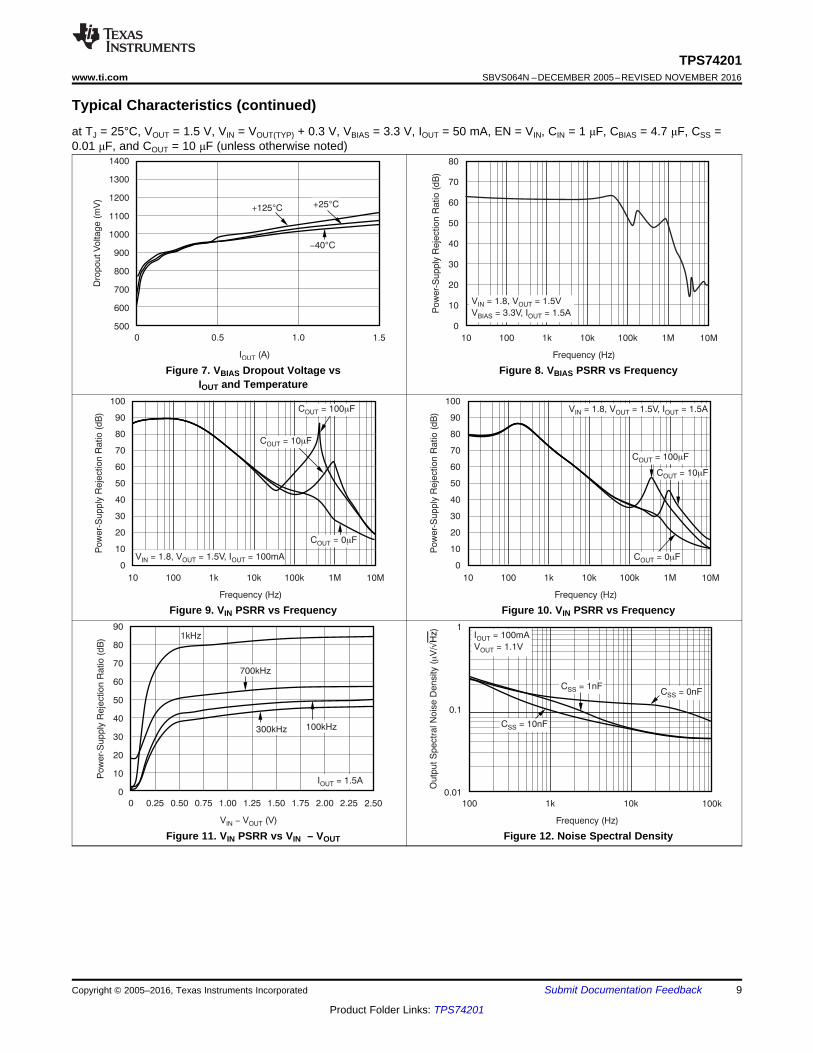
Typical Characteristics (continued)at TJ = 25°C, VOUT = 1.5 V, VIN = VOUT(TYP) + 0.3 V, VBIAS = 3.3 V, IOUT = 50 mA, EN = VIN, CIN = 1 μF, CBIAS = 4.7 μF, CSS =0.01 μF, and COUT = 10 μF (unless otherwise noted)
Figure 7. VBIAS Dropout Voltage vsIOUT and Temperature
Figure 8. VBIAS PSRR vs Frequency
Figure 9. VIN PSRR vs Frequency Figure 10. VIN PSRR vs Frequency
Figure 11. VIN PSRR vs VIN – VOUT Figure 12. Noise Spectral Density

1.0
0.9
0.8
0.7
0.6
0.5
0.4
0.3
0.2
0.1
0
VL
ow
-Le
ve
l P
G V
olta
ge
(V
)O
L
0 2 4 6 8 10 12
PG Current (mA)
10mV/div
10mV/div
10mV/div
10mV/div
1V/div
Time (50 s/div)m
C = 1000 FOUT m
C = 100 FOUT m
C = 10 FOUT m
C = 0 FOUT m
1V/ sm
0.45
0.40
0.35
0.30
0.25
0.20
0.15
0.10
0.05
0
-40 -20 0 20 40 60 80 100
Bia
s C
urr
en
t (
A)
m
Junction Temperature ( C)°
120
V = 2.375VBIAS
V = 5.5VBIAS
765
750
735
720
705
690
675
-40 -20 0 20 40 60 80 100 120
I(n
A)
SS
Junction Temperature ( C)°
2.85
2.65
2.45
2.25
2.05
1.85
1.65
1.45
1.25
0 0.5 1.0
Bia
s C
urr
en
t (m
A)
I (A)OUT
1.5
+125 C°
+25 C°
- °40 C
3.0
2.8
2.6
2.4
2.2
2.0
1.8
1.6
1.4
1.2
1.0
2.0 2.5 3.0 3.5 4.0 4.5
Bia
s C
urr
en
t (m
A)
V (V)BIAS
5.0
+125 C°
+25 C°
- °40 C
10
TPS74201SBVS064N –DECEMBER 2005–REVISED NOVEMBER 2016 www.ti.com
Product Folder Links: TPS74201
Submit Documentation Feedback Copyright © 2005–2016, Texas Instruments Incorporated
Typical Characteristics (continued)at TJ = 25°C, VOUT = 1.5 V, VIN = VOUT(TYP) + 0.3 V, VBIAS = 3.3 V, IOUT = 50 mA, EN = VIN, CIN = 1 μF, CBIAS = 4.7 μF, CSS =0.01 μF, and COUT = 10 μF (unless otherwise noted)
Figure 13. IBIAS vs IOUT and Temperature Figure 14. IBIAS vs VBIAS and VOUT
Figure 15. IBIAS Shutdown vs Temperature Figure 16. Soft-Start Charging Current (ISS) vs Temperature
Figure 17. Low-Level PG Voltage vs PG Current Figure 18. VBIAS Line Transient (1.5 A)

Time (20 s/div)m
VOUT
50mV/divIOUT
500mA/div
Output Open
Output Shorted
1V/div
1V/div
Time (1ms/div)
C = 0 FSS m
C = 0.001 FSS m
C = 0.0047 FSS m
VOUT
VEN
0V
1.2V
1V
/div
Time (20ms/div)
V (500mV/div)PG
VOUT
V = V = VIN BIAS EN
10mV/div
10mV/div
10mV/div
10mV/div
500mV/div
Time (50 s/div)m
C = 2 x 470 F (OSCON)mOUT
C = 100 F (Cer.)OUT m
C = 10 F (Cer.)OUT m
C = 0 FOUT m
1V/ sm
50mV/div
50mV/div
50mV/div
50mV/div
1A/div
Time (50 s/div)m
C = 0 FOUT m
C = 10 F (Cer.)OUT m
C = 100 F (Cer.)OUT m
C = 2 x 470 F (OSCON)OUT m
1A/ sm
1.5A
50mA
11
TPS74201www.ti.com SBVS064N –DECEMBER 2005–REVISED NOVEMBER 2016
Product Folder Links: TPS74201
Submit Documentation FeedbackCopyright © 2005–2016, Texas Instruments Incorporated
Typical Characteristics (continued)at TJ = 25°C, VOUT = 1.5 V, VIN = VOUT(TYP) + 0.3 V, VBIAS = 3.3 V, IOUT = 50 mA, EN = VIN, CIN = 1 μF, CBIAS = 4.7 μF, CSS =0.01 μF, and COUT = 10 μF (unless otherwise noted)
Figure 19. VIN Line Transient Figure 20. Output Load Transient Response
Figure 21. Turnon Response Figure 22. Power Up and Power Down
Figure 23. Output Short Circuit Recovery
Thermal
Limit
Soft-Start
Discharge
OUTVOUT
FB
PG
IN
BIAS
SS
ENHysteresis
and De-Glitch
Current
Limit
UVLO
0.73 Am
0.8V
Reference
0.9 ´ VREF
GND
CSS
R1
R2
V = 0.8 x ( )OUT 1 +R1
R2
12
TPS74201SBVS064N –DECEMBER 2005–REVISED NOVEMBER 2016 www.ti.com
Product Folder Links: TPS74201
Submit Documentation Feedback Copyright © 2005–2016, Texas Instruments Incorporated
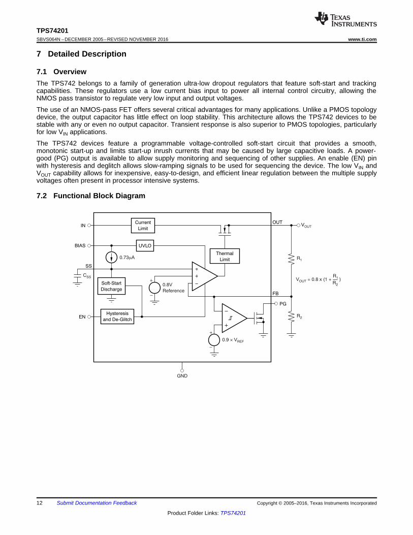
7 Detailed Description
7.1 OverviewThe TPS742 belongs to a family of generation ultra-low dropout regulators that feature soft-start and trackingcapabilities. These regulators use a low current bias input to power all internal control circuitry, allowing theNMOS pass transistor to regulate very low input and output voltages.
The use of an NMOS-pass FET offers several critical advantages for many applications. Unlike a PMOS topologydevice, the output capacitor has little effect on loop stability. This architecture allows the TPS742 devices to bestable with any or even no output capacitor. Transient response is also superior to PMOS topologies, particularlyfor low VIN applications.
The TPS742 devices feature a programmable voltage-controlled soft-start circuit that provides a smooth,monotonic start-up and limits start-up inrush currents that may be caused by large capacitive loads. A power-good (PG) output is available to allow supply monitoring and sequencing of other supplies. An enable (EN) pinwith hysteresis and deglitch allows slow-ramping signals to be used for sequencing the device. The low VIN andVOUT capability allows for inexpensive, easy-to-design, and efficient linear regulation between the multiple supplyvoltages often present in processor intensive systems.
7.2 Functional Block Diagram
13
TPS74201www.ti.com SBVS064N –DECEMBER 2005–REVISED NOVEMBER 2016
Product Folder Links: TPS74201
Submit Documentation FeedbackCopyright © 2005–2016, Texas Instruments Incorporated
7.3 Feature Description
7.3.1 Enable and ShutdownThe enable (EN) pin is active high and is compatible with standard digital signaling levels. VEN less than 0.4 Vturns the regulator off and VEN greater than 1.1 V turns the regulator on. Unlike many regulators, the enablecircuitry has hysteresis and deglitching for use with relatively slow-ramping analog signals. This configurationallows the TPS742 devices to be enabled by connecting the output of another supply to the EN pin. The enablecircuitry typically has 50 mV of hysteresis and a deglitch circuit to help avoid ON and OFF cycling because ofsmall glitches in the VEN signal.
The enable threshold is typically 0.8 V and varies with temperature and process variations. Temperaturevariation is approximately –1 mV/°C; therefore, process variation accounts for most of the variation in the enablethreshold. If precise turnon timing is required, then use a fast rise-time signal to enable the TPS742 devices.
If not used, EN can be connected to either IN or BIAS. If EN is connected to IN, then connect EN as closely aspossible to the largest capacitance on the input to prevent voltage droops on that line from triggering the enablecircuit.
7.3.2 Power-Good (VQFN Packages Only)The power-good (PG) pin is an open-drain output and can be connected to any 5.5 V or lower rail through anexternal pullup resistor. This pin requires at least 1.1 V on VBIAS to have a valid output. The PG output is high-impedance when VOUT is greater than VIT + VHYS. If VOUT drops below VIT or if VBIAS drops less than 1.9 V, theopen-drain output turns on and pulls the PG output low. The PG pin also asserts when the device is disabled.The recommended operating condition of PG pin sink current is up to 1 mA, so the pullup resistor for PG must bein the range of 10 kΩ to 1 MΩ. PG is only provided on the VQFN packages. If output voltage monitoring is notneeded, then the PG pin can be left floating.
7.3.3 Internal Current LimitThe TPS742 family features a factory-trimmed, accurate current limit that is flat over temperature and supplyvoltage. The current limit allows the device to supply surges of up to 1.8 A and maintain regulation. The currentlimit responds in about 10 μs to reduce the current during a short circuit fault. Recovery from a short circuitcondition is well-controlled and results in very little output overshoot when the load is removed. See Figure 23 inthe Typical Characteristics section for a graph of IOUT versus VOUT performance.
The internal current limit protection circuitry of the TPS742 family of devices is designed to protect againstoverload conditions. The circuitry is not intended to allow operation above the rated current of the device.Continuously running the TPS742 devices above the rated current degrades device reliability.
7.4 Device Functional Modes
7.4.1 Normal OperationThe device regulates to the nominal output voltage under the following conditions:
• The input voltage and bias voltage are both at least at the respective minimum specifications.• The enable voltage has previously exceeded the enable rising threshold voltage and has not decreased
below the enable falling threshold.• The output current is less than the current limit.• The device junction temperature is less than the maximum specified junction temperature.• The device is not operating in dropout.
7.4.2 Dropout OperationIf the input voltage is lower than the nominal output voltage plus the specified dropout voltage, but all otherconditions are met for normal operation, the device operates in dropout mode. In this condition, the outputvoltage is the same as the input voltage minus the dropout voltage. The transient performance of the device issignificantly degraded because the pass device is in a triode state and no longer controls the current through theLDO. Line or load transients in dropout can result in large output voltage deviations.

14
TPS74201SBVS064N –DECEMBER 2005–REVISED NOVEMBER 2016 www.ti.com
Product Folder Links: TPS74201
Submit Documentation Feedback Copyright © 2005–2016, Texas Instruments Incorporated
Device Functional Modes (continued)7.4.3 DisabledThe device is disabled under the following conditions:• The input or bias voltages are below the respective minimum specifications.• The enable voltage is less than the enable falling threshold voltage or has not yet exceeded the enable rising
threshold.• The device junction temperature is greater than the thermal shutdown temperature.
Table 1 shows the conditions that lead to the different modes of operation.
Table 1. Device Functional Mode Comparison
OPERATING MODEPARAMETER
VIN VEN VBIAS IOUT TJ
Normal mode VIN > VOUT(nom) + VDO (VIN) VEN > VEN(high) VBIAS ≥ VOUT + 1.4 V I OUT < ICL T J < 125°CDropout mode VIN < VOUT(nom) + VDO (VIN) VEN > VEN(high) VBIAS < VOUT + 1.4 V — TJ < 125°CDisabled mode(any true condition disablesthe device)
VIN < VIN(min) VEN < VEN(low) VBIAS < VBIAS(min) — TJ > 155°C

15
TPS74201www.ti.com SBVS064N –DECEMBER 2005–REVISED NOVEMBER 2016
Product Folder Links: TPS74201
Submit Documentation FeedbackCopyright © 2005–2016, Texas Instruments Incorporated
8 Application and Implementation
NOTEInformation in the following applications sections is not part of the TI componentspecification, and TI does not warrant its accuracy or completeness. TI’s customers areresponsible for determining suitability of components for their purposes. Customers shouldvalidate and test their design implementation to confirm system functionality.
8.1 Application Information
8.1.1 Input, Output, and Bias Capacitor RequirementsThe TPS742 family does not require any output capacitor for stability. If an output capacitor is needed, the deviceis designed to be stable for all available types and values of output capacitance. The device is also stable withmultiple capacitors in parallel, which can be of any type or value.
The capacitance required on the IN and BIAS pins is strongly dependent on the input supply source impedance.To counteract any inductance in the input, the minimum recommended capacitor for VIN and VBIAS is 1μF. If VINand VBIAS are connected to the same supply, the recommended minimum capacitor for VBIAS is 4.7 μF. Use goodquality, low ESR capacitors on the input; ceramic X5R and X7R capacitors are preferred. Place these capacitorsas close to the pins as possible for optimum performance.
8.1.2 Transient ResponseThe TPS742 family of devices were designed to have transient response within 5% for most applications withoutany output capacitor. In some cases, the transient response may be limited by the transient response of the inputsupply. This limitation is especially true in applications where the difference between the input and output is lessthan 300 mV. In this case, adding additional input capacitance improves the transient response much more thanjust adding additional output capacitance would do. With a solid input supply, adding additional outputcapacitance reduces undershoot and overshoot during a transient at the expense of a slightly longer VOUTrecovery time. See Figure 20 in the Typical Characteristics section. Because the TPS742 devices are stablewithout an output capacitor, many applications may allow for little or no capacitance at the LDO output. For theseapplications, local bypass capacitance for the device under power may be sufficient to meet the transientrequirements of the application. This design reduces the total solution cost by avoiding the need to useexpensive high-value capacitors at the LDO output.
8.1.3 Dropout VoltageThe TPS742 family of devices offers industry-leading dropout performance, making this family well-suited forhigh-current low VIN/low VOUT applications. The extremely low dropout of the TPS742 allows the device to beused in place of a DC-DC converter and still achieve good efficiency. This efficiency allows the user to rethinkthe power architecture for their applications to achieve the smallest, simplest, and lowest cost solution.
There are two different specifications for dropout voltage with the TPS742 devices. The first specification(illustrated in Figure 24) is referred to as VIN Dropout, and is for users who wish to apply an external bias voltageto achieve low dropout. This specification assumes that VBIAS is at least 1.62 V above VOUT, which is the case forVBIAS when powered by a 3.3-V rail with 5% tolerance and with VOUT = 1.5 V. If VBIAS is higher than 3.3 V × 0.95or VOUT is less than 1.5 V, VIN dropout is less than specified.

( ) RMSN RMS OUT
VV V 25 V (V)
V
mæ öm = ´ç ÷
è ø
Reference
Simplified Block Diagram
VOUTOUT
BIAS
FB
IN
VIN
V = 3.3V 5%BIAS ±
V = 3.3V 5V
V = 1.5V
I = 1.5A
Efficiency = 45%
IN
OUT
OUT
±
Reference
Simplified Block Diagram
VOUTOUT
BIAS
FB
INV = 5V 5%BIAS ±
V = 1.8V
V = 1.5V
I = 1.5A
Efficiency = 83%
IN
OUT
OUT
16
TPS74201SBVS064N –DECEMBER 2005–REVISED NOVEMBER 2016 www.ti.com
Product Folder Links: TPS74201
Submit Documentation Feedback Copyright © 2005–2016, Texas Instruments Incorporated
Application Information (continued)
Figure 24. Typical Application of the TPS742 Using an Auxiliary Bias Rail
The second specification (shown in Figure 25) is referred to as VBIAS Dropout, and is for users who wish to tie INand BIAS together. This option allows the device to be used in applications where an auxiliary bias voltage is notavailable or low dropout is not required. Dropout is limited by BIAS in these applications because VBIAS providesthe gate drive to the pass FET and therefore must be 1.4 V above VOUT. Because of this usage, IN and BIAS tiedtogether easily consume huge power. Pay attention not to exceed the power rating of the IC package.
Figure 25. Typical Application of the TPS742 Without an Auxiliary Bias
8.1.4 Output NoiseThe TPS742 devices provide low-output noise when a soft-start capacitor is used. When the device reaches theend of the soft-start cycle, the soft-start capacitor serves as a filter for the internal reference. By using a 0.001-μFsoft-start capacitor, the output noise is reduced by half and is typically 30 μVRMS for a 1.2-V output (10 Hz to100 kHz). Because most of the output noise is generated by the internal reference, the noise is a function of theset output voltage. The RMS noise with a 0.001-μF soft-start capacitor is given in Equation 1.
(1)
The low-output noise of the TPS742 makes the device a good choice for powering transceivers, PLLs, or othernoise-sensitive circuitry.
t (s) =SS
V C
IREF SS
SS
× 0.8V C (F)
0.73 ASS
m
×=
( )OUT(NOM) OUT
SSCLCL(MIN)
V Ct
I
´=
( )REF SS
SS
SS
V Ct
I
´=
17
TPS74201www.ti.com SBVS064N –DECEMBER 2005–REVISED NOVEMBER 2016
Product Folder Links: TPS74201
Submit Documentation FeedbackCopyright © 2005–2016, Texas Instruments Incorporated
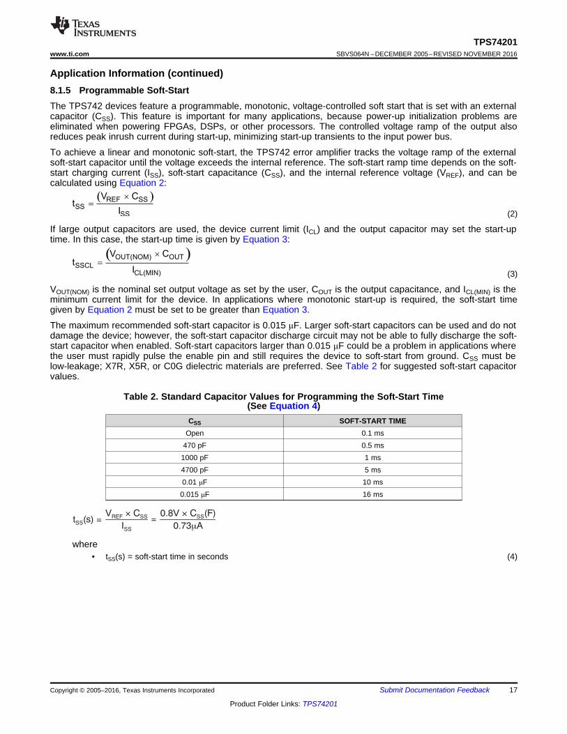
Application Information (continued)8.1.5 Programmable Soft-StartThe TPS742 devices feature a programmable, monotonic, voltage-controlled soft start that is set with an externalcapacitor (CSS). This feature is important for many applications, because power-up initialization problems areeliminated when powering FPGAs, DSPs, or other processors. The controlled voltage ramp of the output alsoreduces peak inrush current during start-up, minimizing start-up transients to the input power bus.
To achieve a linear and monotonic soft-start, the TPS742 error amplifier tracks the voltage ramp of the externalsoft-start capacitor until the voltage exceeds the internal reference. The soft-start ramp time depends on the soft-start charging current (ISS), soft-start capacitance (CSS), and the internal reference voltage (VREF), and can becalculated using Equation 2:
(2)
If large output capacitors are used, the device current limit (ICL) and the output capacitor may set the start-uptime. In this case, the start-up time is given by Equation 3:
(3)
VOUT(NOM) is the nominal set output voltage as set by the user, COUT is the output capacitance, and ICL(MIN) is theminimum current limit for the device. In applications where monotonic start-up is required, the soft-start timegiven by Equation 2 must be set to be greater than Equation 3.
The maximum recommended soft-start capacitor is 0.015 μF. Larger soft-start capacitors can be used and do notdamage the device; however, the soft-start capacitor discharge circuit may not be able to fully discharge the soft-start capacitor when enabled. Soft-start capacitors larger than 0.015 μF could be a problem in applications wherethe user must rapidly pulse the enable pin and still requires the device to soft-start from ground. CSS must below-leakage; X7R, X5R, or C0G dielectric materials are preferred. See Table 2 for suggested soft-start capacitorvalues.
Table 2. Standard Capacitor Values for Programming the Soft-Start Time(See Equation 4)
CSS SOFT-START TIMEOpen 0.1 ms
470 pF 0.5 ms1000 pF 1 ms4700 pF 5 ms0.01 μF 10 ms0.015 μF 16 ms
where• tSS(s) = soft-start time in seconds (4)

TPS74201
GND SS
OUT
FB
EN
IN
BIAS
VIN V
OUT
R2
R1
CSS
CIN
1 Fm
C
VBIAS
CBIAS
1 Fm
R
18
TPS74201SBVS064N –DECEMBER 2005–REVISED NOVEMBER 2016 www.ti.com
Product Folder Links: TPS74201
Submit Documentation Feedback Copyright © 2005–2016, Texas Instruments Incorporated
8.1.6 Sequencing RequirementsThe device can have VIN, VBIAS, and VEN sequenced in any order without causing damage to the device.However, for the soft-start function to work as intended, certain sequencing rules must be applied. Enabling thedevice after VIN and VBIAS are present is preferred, and can be accomplished using a digital output from aprocessor or supply supervisor. An analog signal from an external RC circuit, as shown in Figure 26, can also beused as long as the delay time is long enough for VIN and VBIAS to be present.
Figure 26. Soft-Start Delay Using an RC Circuit on Enable
If a signal is not available to enable the device after IN and BIAS, simply connecting EN to IN is acceptable formost applications as long as VIN is greater than 1.1 V and the ramp rate of VIN and VBIAS is faster the set soft-start ramp rate. If the ramp rate of the input sources is slower than the set soft-start time, the output tracks theslower supply minus the dropout voltage until the set output voltage is reached. If EN is connected to BIAS, thedevice does soft-start as programmed provided that VIN is present before VBIAS. If VBIAS and VEN are presentbefore VIN is applied and the set soft-start time has expired then VOUT tracks VIN.
NOTEWhen VBIAS and VEN are present and VIN is not supplied, this device outputs approximately50 μA of current from OUT. Although this condition will not cause any damage to thedevice, the output current may charge up the OUT node if total resistance between OUTand GND (including external feedback resistors) is greater than 10 kΩ..

TPS74201
GND
EN
FB
IN PG
BIAS
SS
OUT
VIN
VOUT
R1
R2
R3
COUT
Optional
CIN
1 Fm
CSS
VBIAS
CBIAS
1 Fm
V = 0.8OUT ´ 1 +R1
R2( )
19
TPS74201www.ti.com SBVS064N –DECEMBER 2005–REVISED NOVEMBER 2016
Product Folder Links: TPS74201
Submit Documentation FeedbackCopyright © 2005–2016, Texas Instruments Incorporated
8.2 Typical ApplicationsFigure 27 is a typical application circuit for the TPS742 adjustable output device.
R1 and R2 can be calculated for any output voltage using the formula shown in Figure 27. See Table 3 forsample resistor values of common output voltages. To achieve the maximum accuracy specifications, R2 must be≤ 4.99 kΩ.
Figure 27. Typical Application Circuit for the TPS742
Table 3. Standard 1% Resistor Values for Programming the Output Voltage(See Equation 5)
R1 (kΩ) R2 (kΩ) VOUT (V)Short Open 0.80.619 4.99 0.91.13 4.53 11.37 4.42 1.051.87 4.99 1.12.49 4.99 1.24.12 4.75 1.53.57 2.87 1.83.57 1.69 2.53.57 1.15 3.3
VOUT = 0.8 × (1 + R1/R2) (5)
NOTEWhen VBIAS and VEN are present and VIN is not supplied, this device outputs approximately50 μA of current from OUT. Although this condition does not cause any damage to thedevice, the output current can charge up the OUT node if total resistance between OUTand GND (including external feedback resistors) is greater than 10 kΩ.
8.2.1 Design RequirementsThe design goals are VIN = 1.8 V, VOUT = 1.5 V, and IOUT = 1 A (maximum). The design optimizes transientresponse and meets a 1-ms start-up time with a start-up dominated by the soft-start feature. The input supplycomes from a supply on the same circuit board. The available system rails for VBIAS are 2.7 V, 3.3 V, and 5 V.
The design space consists of CIN, COUT, CBIAS, CSS, VBIAS, R1, R2, and R3, and the circuit is from Figure 27.
This example uses a VIN of 1.8 V, with a VBIAS of 2.5 V.

1V/div
1V/div
Time (1ms/div)
C = 0 FSS m
C = 0.001 FSS m
C = 0.0047 FSS m
VOUT
VEN
0V
1.2V
50mV/div
50mV/div
50mV/div
50mV/div
1A/div
Time (50 s/div)m
C = 0 FOUT m
C = 10 F (Cer.)OUT m
C = 100 F (Cer.)OUT m
C = 2 x 470 F (OSCON)OUT m
1A/ sm
1.5A
50mA
100
75
50
25
0
0 0.5 1.0
Dro
po
ut
Vo
lta
ge
(m
V)
I (A)OUT
1.5
+125 C°
+25 C°
- °40 C
10mV/div
10mV/div
10mV/div
10mV/div
1V/div
Time (50 s/div)m
C = 1000 FOUT m
C = 100 FOUT m
C = 10 FOUT m
C = 0 FOUT m
1V/ sm
20
TPS74201SBVS064N –DECEMBER 2005–REVISED NOVEMBER 2016 www.ti.com
Product Folder Links: TPS74201
Submit Documentation Feedback Copyright © 2005–2016, Texas Instruments Incorporated
8.2.2 Detailed Design ProcedureThis is assuming the table for the standard capacitor values is put back in as Table 1.
Utilizing Table 3, we select R1 = 4.12 kΩ for VOUT = 1.5 V. and R2 = 4.75 kΩ. Using Table 1, we select CSS =1000 pF for a 1-ms typical start-up time. For optimal performance, we use the 5-V rail for a Bias supply. An R3 of100 kΩ is selected as the PG bus is used by other devices with additional 100-kΩ pullup resistors.
A CIN of 10 µF is used for better transient performance on the input supply, a CBIAS of 1 µF is used to ensure theBias supply is solid, and a COUT of 1 µF is used to provide some local capacitance on the output.
8.2.3 Application Curves
Figure 28. VIN Dropout Voltage vsIOUT and Temperature (TJ)
Figure 29. VBIAS Line Transient (1.5 A)
Figure 30. Output Load Transient Response Figure 31. Turnon Response
9 Power Supply RecommendationsThe TPS742 devices are designed to operate from an input voltage from 1.1 V to 5.5 V, provided the bias rail isat least 1.4-V higher than the input supply. The bias rail and the input supply must both provide adequateheadroom and current for the device to operate normally.
Connect a low-output impedance power supply directly to the IN pin of the TPS742 devices. This supply musthave at least 1 µF of capacitance near the IN pin for stability. A supply with similar requirements must also beconnected directly to the bias rail with a separate 1 µF or larger capacitor.
If the IN pin is tied to the bias pin, a minimum 4.7 µF of capacitance is needed for stability.
To increase the overall PSRR of the solution at higher frequencies, use a pi-filter or ferrite bead before the inputcapacitor.

2
15
17
20
15
11
10
6
9
8
3
18
4
7 19
12 13 1414
16
OUT
OUT
NC
OUT
OU
T
NC
NC
NCIN
FB/SNS
IN
IN
PG
IN
BIAS
SSNC
NC
GN
D
EN
Css
Cbias
R(pull-up)
R1
R2
Cin
Cout
R1 & R2 should be connected close to the load, Cout should be as near to
the LDO as possible
Input GND Plane
Vin Plane
Vout Plane
Output GND Plane
Thermal Pad
Keep the ground planes on the same side of the PCB if possible to improve thermal
disappation
21
TPS74201www.ti.com SBVS064N –DECEMBER 2005–REVISED NOVEMBER 2016
Product Folder Links: TPS74201
Submit Documentation FeedbackCopyright © 2005–2016, Texas Instruments Incorporated
10 Layout
10.1 Layout GuidelinesAn optimal layout can greatly improve transient performance, PSRR, and noise. To minimize the voltage droopon the input of the device during load transients, connect the capacitance on IN and BIAS as close as possible tothe device. This capacitance also minimizes the effects of parasitic inductance and resistance of the input sourceand can therefore improve stability. To achieve optimal transient performance and accuracy, connect the top sideof R1 in Figure 27 as close as possible to the load. If BIAS is connected to IN, TI recommends connecting BIASas close to the sense point of the input supply as possible. This connection minimizes the voltage droop on BIASduring transient conditions and can improve the turnon response.
10.2 Layout Example
Figure 32. Layout Schematic (VQFN Packages)
Y YJT J T JT D
: T = T + P·
Y YJB J B JB D
: T = T + P·
22
TPS74201SBVS064N –DECEMBER 2005–REVISED NOVEMBER 2016 www.ti.com
Product Folder Links: TPS74201
Submit Documentation Feedback Copyright © 2005–2016, Texas Instruments Incorporated
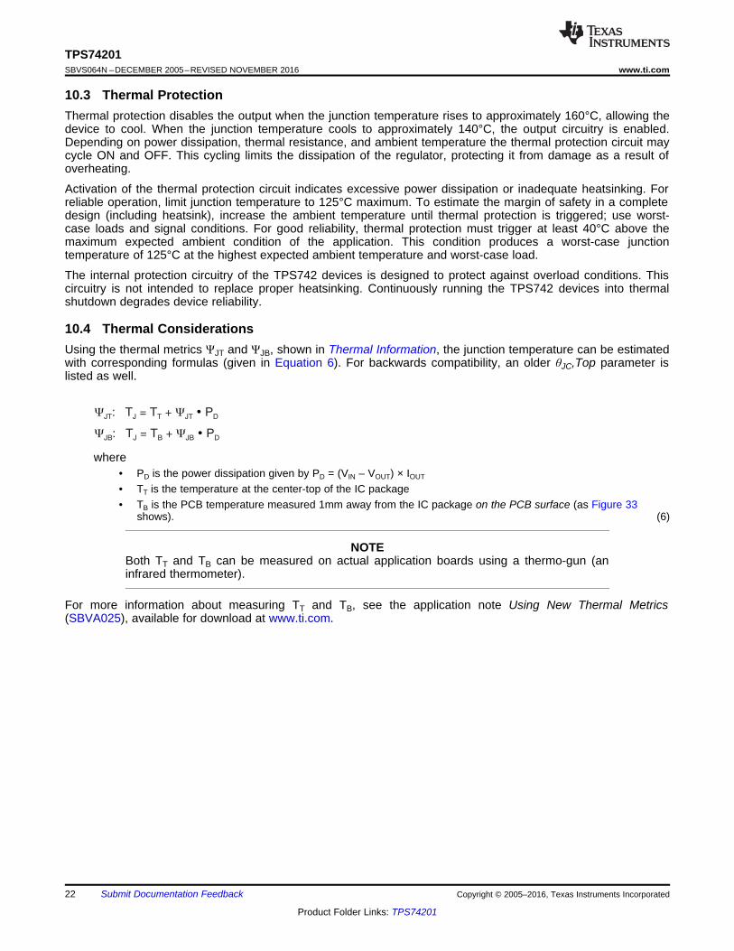
10.3 Thermal ProtectionThermal protection disables the output when the junction temperature rises to approximately 160°C, allowing thedevice to cool. When the junction temperature cools to approximately 140°C, the output circuitry is enabled.Depending on power dissipation, thermal resistance, and ambient temperature the thermal protection circuit maycycle ON and OFF. This cycling limits the dissipation of the regulator, protecting it from damage as a result ofoverheating.
Activation of the thermal protection circuit indicates excessive power dissipation or inadequate heatsinking. Forreliable operation, limit junction temperature to 125°C maximum. To estimate the margin of safety in a completedesign (including heatsink), increase the ambient temperature until thermal protection is triggered; use worst-case loads and signal conditions. For good reliability, thermal protection must trigger at least 40°C above themaximum expected ambient condition of the application. This condition produces a worst-case junctiontemperature of 125°C at the highest expected ambient temperature and worst-case load.
The internal protection circuitry of the TPS742 devices is designed to protect against overload conditions. Thiscircuitry is not intended to replace proper heatsinking. Continuously running the TPS742 devices into thermalshutdown degrades device reliability.
10.4 Thermal ConsiderationsUsing the thermal metrics ΨJT and ΨJB, shown in Thermal Information, the junction temperature can be estimatedwith corresponding formulas (given in Equation 6). For backwards compatibility, an older θJC,Top parameter islisted as well.
where• PD is the power dissipation given by PD = (VIN – VOUT) × IOUT
• TT is the temperature at the center-top of the IC package• TB is the PCB temperature measured 1mm away from the IC package on the PCB surface (as Figure 33
shows). (6)
NOTEBoth TT and TB can be measured on actual application boards using a thermo-gun (aninfrared thermometer).
For more information about measuring TT and TB, see the application note Using New Thermal Metrics(SBVA025), available for download at www.ti.com.

T on PCBBT on of ICtopT
1mm
(a) Example RGW (QFN) Package Measurement (b) Example KTW (DDPAK) Package Measurement
1mm
T on of ICT top(1)
T on PCB
surface
B
(2)
23
TPS74201www.ti.com SBVS064N –DECEMBER 2005–REVISED NOVEMBER 2016
Product Folder Links: TPS74201
Submit Documentation FeedbackCopyright © 2005–2016, Texas Instruments Incorporated
Thermal Considerations (continued)
(1) TT is measured at the center of both the X- and Y-dimensional axes.(2) TB is measured below the package lead on the PCB surface.
Figure 33. Measuring Points for TT and TB

12
10
8
6
4
2
0
YY
and
(C
/W)
JT
JB
°
0 2 4 6 8 10
Board Copper Area (in )2
YJT (KTW)
YJT (RGW)
YJB (RGW)
YJB (KTW)
24
TPS74201SBVS064N –DECEMBER 2005–REVISED NOVEMBER 2016 www.ti.com
Product Folder Links: TPS74201
Submit Documentation Feedback Copyright © 2005–2016, Texas Instruments Incorporated
Thermal Considerations (continued)Compared with θJA, the new thermal metrics ΨJT and ΨJB are less independent of board size, but they do have asmall dependency. Figure 34 shows characteristic performance of ΨJT and ΨJB versus board size.
Looking at Figure 34, the RGW package thermal performance has negligible dependency on board size. TheKTW package, however, does have a measurable dependency on board size. This dependency exists becausethe package shape is not point-symmetric to an IC center. In the KTW package, for example (see Figure 33),silicon is not beneath the measuring point of TT, which is the center of the X and Y dimension, so that ΨJT has adependency. Also, because of that non-point-symmetry, device heat distribution on the PCB is not point-symmetric, either, so that ΨJB has a dependency.
space
Figure 34. ΨJT and ΨJB vs Board Size
For a more detailed discussion of why TI does not recommend using θJC,Top to determine thermalcharacteristics, refer to the application note Using New Thermal Metrics (SBVA025), available for download atwww.ti.com. Also, refer to the application note IC Package Thermal Metrics (SPRA953) (also available on the TIwebsite) for further information.

25
TPS74201www.ti.com SBVS064N –DECEMBER 2005–REVISED NOVEMBER 2016
Product Folder Links: TPS74201
Submit Documentation FeedbackCopyright © 2005–2016, Texas Instruments Incorporated
11 Device and Documentation Support
11.1 Device Support
11.1.1 Development Support
11.1.1.1 Evaluation ModulesAn evaluation module (EVM) is available to assist in the initial circuit performance evaluation using the TPS744.The TPS74201EVM-118 evaluation module (and related user guide) can be requested at the Texas Instrumentswebsite through the product folders or purchased directly from the TI eStore.
11.1.1.2 Spice ModelsComputer simulation of circuit performance using SPICE is often useful when analyzing the performance ofanalog circuits and systems. A SPICE model for the TPS744 is available through the product folders under Tools& Software.
11.2 Documentation Support
11.2.1 Related DocumentationFor related documentation see the following:• 6A Current-Sharing Dual LDO• Using New Thermal Metrics Application Report
11.3 Receiving Notification of Documentation UpdatesTo receive notification of documentation updates, navigate to the device product folder on ti.com. In the upperright corner, click on Alert me to register and receive a weekly digest of any product information that haschanged. For change details, review the revision history included in any revised document.
11.4 Community ResourcesThe following links connect to TI community resources. Linked contents are provided "AS IS" by the respectivecontributors. They do not constitute TI specifications and do not necessarily reflect TI's views; see TI's Terms ofUse.
TI E2E™ Online Community TI's Engineer-to-Engineer (E2E) Community. Created to foster collaborationamong engineers. At e2e.ti.com, you can ask questions, share knowledge, explore ideas and helpsolve problems with fellow engineers.
Design Support TI's Design Support Quickly find helpful E2E forums along with design support tools andcontact information for technical support.
11.5 TrademarksE2E is a trademark of Texas Instruments.All other trademarks are the property of their respective owners.
11.6 Electrostatic Discharge CautionThese devices have limited built-in ESD protection. The leads should be shorted together or the device placed in conductive foamduring storage or handling to prevent electrostatic damage to the MOS gates.
11.7 GlossarySLYZ022 — TI Glossary.
This glossary lists and explains terms, acronyms, and definitions.

26
TPS74201SBVS064N –DECEMBER 2005–REVISED NOVEMBER 2016 www.ti.com
Product Folder Links: TPS74201
Submit Documentation Feedback Copyright © 2005–2016, Texas Instruments Incorporated
12 Mechanical, Packaging, and Orderable InformationThe following pages include mechanical, packaging, and orderable information. This information is the mostcurrent data available for the designated devices. This data is subject to change without notice and revision ofthis document. For browser-based versions of this data sheet, refer to the left-hand navigation.

PACKAGE OPTION ADDENDUM
www.ti.com 6-Dec-2016
Addendum-Page 1
PACKAGING INFORMATION
Orderable Device Status(1)
Package Type PackageDrawing
Pins PackageQty
Eco Plan(2)
Lead/Ball Finish(6)
MSL Peak Temp(3)
Op Temp (°C) Device Marking(4/5)
Samples
TPS74201KTWR ACTIVE DDPAK/TO-263
KTW 7 500 Green (RoHS& no Sb/Br)
CU SN Level-3-245C-168 HR -40 to 85 TPS74201
TPS74201KTWRG3 ACTIVE DDPAK/TO-263
KTW 7 500 Green (RoHS& no Sb/Br)
CU SN Level-3-245C-168 HR -40 to 85 TPS74201
TPS74201KTWT ACTIVE DDPAK/TO-263
KTW 7 50 Green (RoHS& no Sb/Br)
CU SN Level-3-245C-168 HR -40 to 85 TPS74201
TPS74201KTWTG3 ACTIVE DDPAK/TO-263
KTW 7 50 Green (RoHS& no Sb/Br)
CU SN Level-3-245C-168 HR -40 to 85 TPS74201
TPS74201RGRR ACTIVE VQFN RGR 20 3000 Green (RoHS& no Sb/Br)
CU NIPDAU Level-2-260C-1 YEAR -40 to 125 12JA
TPS74201RGRT ACTIVE VQFN RGR 20 250 Green (RoHS& no Sb/Br)
CU NIPDAU Level-2-260C-1 YEAR -40 to 125 12JA
TPS74201RGWR ACTIVE VQFN RGW 20 3000 Green (RoHS& no Sb/Br)
CU NIPDAU Level-2-260C-1 YEAR -40 to 85 TPS74201
TPS74201RGWRG4 ACTIVE VQFN RGW 20 3000 Green (RoHS& no Sb/Br)
CU NIPDAU Level-2-260C-1 YEAR -40 to 85 TPS74201
TPS74201RGWT ACTIVE VQFN RGW 20 250 Green (RoHS& no Sb/Br)
CU NIPDAU Level-2-260C-1 YEAR -40 to 85 TPS74201
TPS74201RGWTG4 ACTIVE VQFN RGW 20 250 Green (RoHS& no Sb/Br)
CU NIPDAU Level-2-260C-1 YEAR -40 to 85 TPS74201
(1) The marketing status values are defined as follows:ACTIVE: Product device recommended for new designs.LIFEBUY: TI has announced that the device will be discontinued, and a lifetime-buy period is in effect.NRND: Not recommended for new designs. Device is in production to support existing customers, but TI does not recommend using this part in a new design.PREVIEW: Device has been announced but is not in production. Samples may or may not be available.OBSOLETE: TI has discontinued the production of the device.
(2) Eco Plan - The planned eco-friendly classification: Pb-Free (RoHS), Pb-Free (RoHS Exempt), or Green (RoHS & no Sb/Br) - please check http://www.ti.com/productcontent for the latest availabilityinformation and additional product content details.TBD: The Pb-Free/Green conversion plan has not been defined.Pb-Free (RoHS): TI's terms "Lead-Free" or "Pb-Free" mean semiconductor products that are compatible with the current RoHS requirements for all 6 substances, including the requirement thatlead not exceed 0.1% by weight in homogeneous materials. Where designed to be soldered at high temperatures, TI Pb-Free products are suitable for use in specified lead-free processes.Pb-Free (RoHS Exempt): This component has a RoHS exemption for either 1) lead-based flip-chip solder bumps used between the die and package, or 2) lead-based die adhesive used betweenthe die and leadframe. The component is otherwise considered Pb-Free (RoHS compatible) as defined above.Green (RoHS & no Sb/Br): TI defines "Green" to mean Pb-Free (RoHS compatible), and free of Bromine (Br) and Antimony (Sb) based flame retardants (Br or Sb do not exceed 0.1% by weightin homogeneous material)

PACKAGE OPTION ADDENDUM
www.ti.com 6-Dec-2016
Addendum-Page 2
(3) MSL, Peak Temp. - The Moisture Sensitivity Level rating according to the JEDEC industry standard classifications, and peak solder temperature.
(4) There may be additional marking, which relates to the logo, the lot trace code information, or the environmental category on the device.
(5) Multiple Device Markings will be inside parentheses. Only one Device Marking contained in parentheses and separated by a "~" will appear on a device. If a line is indented then it is a continuationof the previous line and the two combined represent the entire Device Marking for that device.
(6) Lead/Ball Finish - Orderable Devices may have multiple material finish options. Finish options are separated by a vertical ruled line. Lead/Ball Finish values may wrap to two lines if the finishvalue exceeds the maximum column width.
Important Information and Disclaimer:The information provided on this page represents TI's knowledge and belief as of the date that it is provided. TI bases its knowledge and belief on informationprovided by third parties, and makes no representation or warranty as to the accuracy of such information. Efforts are underway to better integrate information from third parties. TI has taken andcontinues to take reasonable steps to provide representative and accurate information but may not have conducted destructive testing or chemical analysis on incoming materials and chemicals.TI and TI suppliers consider certain information to be proprietary, and thus CAS numbers and other limited information may not be available for release.
In no event shall TI's liability arising out of such information exceed the total purchase price of the TI part(s) at issue in this document sold by TI to Customer on an annual basis.
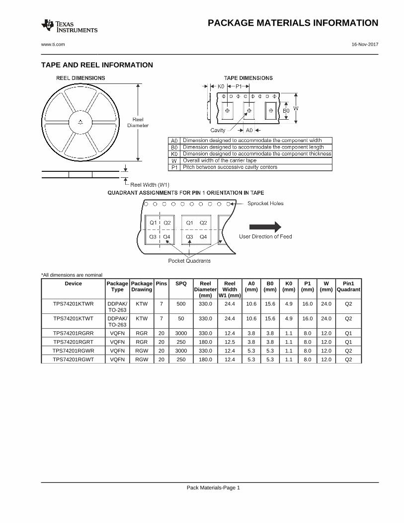
TAPE AND REEL INFORMATION
*All dimensions are nominal
Device PackageType
PackageDrawing
Pins SPQ ReelDiameter
(mm)
ReelWidth
W1 (mm)
A0(mm)
B0(mm)
K0(mm)
P1(mm)
W(mm)
Pin1Quadrant
TPS74201KTWR DDPAK/TO-263
KTW 7 500 330.0 24.4 10.6 15.6 4.9 16.0 24.0 Q2
TPS74201KTWT DDPAK/TO-263
KTW 7 50 330.0 24.4 10.6 15.6 4.9 16.0 24.0 Q2
TPS74201RGRR VQFN RGR 20 3000 330.0 12.4 3.8 3.8 1.1 8.0 12.0 Q1
TPS74201RGRT VQFN RGR 20 250 180.0 12.5 3.8 3.8 1.1 8.0 12.0 Q1
TPS74201RGWR VQFN RGW 20 3000 330.0 12.4 5.3 5.3 1.1 8.0 12.0 Q2
TPS74201RGWT VQFN RGW 20 250 180.0 12.4 5.3 5.3 1.1 8.0 12.0 Q2
PACKAGE MATERIALS INFORMATION
www.ti.com 16-Nov-2017
Pack Materials-Page 1

*All dimensions are nominal
Device Package Type Package Drawing Pins SPQ Length (mm) Width (mm) Height (mm)
TPS74201KTWR DDPAK/TO-263 KTW 7 500 367.0 367.0 45.0
TPS74201KTWT DDPAK/TO-263 KTW 7 50 367.0 367.0 45.0
TPS74201RGRR VQFN RGR 20 3000 338.0 355.0 50.0
TPS74201RGRT VQFN RGR 20 250 338.0 355.0 50.0
TPS74201RGWR VQFN RGW 20 3000 367.0 367.0 35.0
TPS74201RGWT VQFN RGW 20 250 210.0 185.0 35.0
PACKAGE MATERIALS INFORMATION
www.ti.com 16-Nov-2017
Pack Materials-Page 2
MECHANICAL DATA
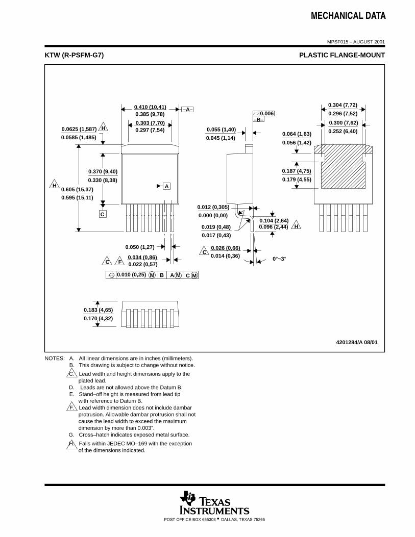
MPSF015 – AUGUST 2001
POST OFFICE BOX 655303 • DALLAS, TEXAS 75265
KTW (R-PSFM-G7) PLASTIC FLANGE-MOUNT
0.010 (0,25) A M
4201284/A 08/01
0.385 (9,78)0.410 (10,41)
M MB C
–A–0.006
–B–
0.170 (4,32)
0.183 (4,65)
0.000 (0,00)
0.012 (0,305)
0.104 (2,64)0.096 (2,44)
0.034 (0,86)0.022 (0,57)
0.050 (1,27)
0.055 (1,40)
0.045 (1,14)
0.014 (0,36)0.026 (0,66)
0.330 (8,38)
0.370 (9,40)
0.297 (7,54)0.303 (7,70)
0.0585 (1,485)
0.0625 (1,587)
0.595 (15,11)
0.605 (15,37)
0.019 (0,48)
0.017 (0,43)
0°~3°
0.179 (4,55)
0.187 (4,75)
0.056 (1,42)
0.064 (1,63)
0.296 (7,52)
0.304 (7,72)
0.300 (7,62)
0.252 (6,40)
F
C
C
H
H
H
C
A
NOTES: A. All linear dimensions are in inches (millimeters).B. This drawing is subject to change without notice.
C. Lead width and height dimensions apply to theplated lead.
D. Leads are not allowed above the Datum B.E. Stand–off height is measured from lead tip
with reference to Datum B.F. Lead width dimension does not include dambar
protrusion. Allowable dambar protrusion shall notcause the lead width to exceed the maximumdimension by more than 0.003”.
G. Cross–hatch indicates exposed metal surface.
H. Falls within JEDEC MO–169 with the exceptionof the dimensions indicated.


IMPORTANT NOTICE
Texas Instruments Incorporated (TI) reserves the right to make corrections, enhancements, improvements and other changes to itssemiconductor products and services per JESD46, latest issue, and to discontinue any product or service per JESD48, latest issue. Buyersshould obtain the latest relevant information before placing orders and should verify that such information is current and complete.TI’s published terms of sale for semiconductor products (http://www.ti.com/sc/docs/stdterms.htm) apply to the sale of packaged integratedcircuit products that TI has qualified and released to market. Additional terms may apply to the use or sale of other types of TI products andservices.Reproduction of significant portions of TI information in TI data sheets is permissible only if reproduction is without alteration and isaccompanied by all associated warranties, conditions, limitations, and notices. TI is not responsible or liable for such reproduceddocumentation. Information of third parties may be subject to additional restrictions. Resale of TI products or services with statementsdifferent from or beyond the parameters stated by TI for that product or service voids all express and any implied warranties for theassociated TI product or service and is an unfair and deceptive business practice. TI is not responsible or liable for any such statements.Buyers and others who are developing systems that incorporate TI products (collectively, “Designers”) understand and agree that Designersremain responsible for using their independent analysis, evaluation and judgment in designing their applications and that Designers havefull and exclusive responsibility to assure the safety of Designers' applications and compliance of their applications (and of all TI productsused in or for Designers’ applications) with all applicable regulations, laws and other applicable requirements. Designer represents that, withrespect to their applications, Designer has all the necessary expertise to create and implement safeguards that (1) anticipate dangerousconsequences of failures, (2) monitor failures and their consequences, and (3) lessen the likelihood of failures that might cause harm andtake appropriate actions. Designer agrees that prior to using or distributing any applications that include TI products, Designer willthoroughly test such applications and the functionality of such TI products as used in such applications.TI’s provision of technical, application or other design advice, quality characterization, reliability data or other services or information,including, but not limited to, reference designs and materials relating to evaluation modules, (collectively, “TI Resources”) are intended toassist designers who are developing applications that incorporate TI products; by downloading, accessing or using TI Resources in anyway, Designer (individually or, if Designer is acting on behalf of a company, Designer’s company) agrees to use any particular TI Resourcesolely for this purpose and subject to the terms of this Notice.TI’s provision of TI Resources does not expand or otherwise alter TI’s applicable published warranties or warranty disclaimers for TIproducts, and no additional obligations or liabilities arise from TI providing such TI Resources. TI reserves the right to make corrections,enhancements, improvements and other changes to its TI Resources. TI has not conducted any testing other than that specificallydescribed in the published documentation for a particular TI Resource.Designer is authorized to use, copy and modify any individual TI Resource only in connection with the development of applications thatinclude the TI product(s) identified in such TI Resource. NO OTHER LICENSE, EXPRESS OR IMPLIED, BY ESTOPPEL OR OTHERWISETO ANY OTHER TI INTELLECTUAL PROPERTY RIGHT, AND NO LICENSE TO ANY TECHNOLOGY OR INTELLECTUAL PROPERTYRIGHT OF TI OR ANY THIRD PARTY IS GRANTED HEREIN, including but not limited to any patent right, copyright, mask work right, orother intellectual property right relating to any combination, machine, or process in which TI products or services are used. Informationregarding or referencing third-party products or services does not constitute a license to use such products or services, or a warranty orendorsement thereof. Use of TI Resources may require a license from a third party under the patents or other intellectual property of thethird party, or a license from TI under the patents or other intellectual property of TI.TI RESOURCES ARE PROVIDED “AS IS” AND WITH ALL FAULTS. TI DISCLAIMS ALL OTHER WARRANTIES ORREPRESENTATIONS, EXPRESS OR IMPLIED, REGARDING RESOURCES OR USE THEREOF, INCLUDING BUT NOT LIMITED TOACCURACY OR COMPLETENESS, TITLE, ANY EPIDEMIC FAILURE WARRANTY AND ANY IMPLIED WARRANTIES OFMERCHANTABILITY, FITNESS FOR A PARTICULAR PURPOSE, AND NON-INFRINGEMENT OF ANY THIRD PARTY INTELLECTUALPROPERTY RIGHTS. TI SHALL NOT BE LIABLE FOR AND SHALL NOT DEFEND OR INDEMNIFY DESIGNER AGAINST ANY CLAIM,INCLUDING BUT NOT LIMITED TO ANY INFRINGEMENT CLAIM THAT RELATES TO OR IS BASED ON ANY COMBINATION OFPRODUCTS EVEN IF DESCRIBED IN TI RESOURCES OR OTHERWISE. IN NO EVENT SHALL TI BE LIABLE FOR ANY ACTUAL,DIRECT, SPECIAL, COLLATERAL, INDIRECT, PUNITIVE, INCIDENTAL, CONSEQUENTIAL OR EXEMPLARY DAMAGES INCONNECTION WITH OR ARISING OUT OF TI RESOURCES OR USE THEREOF, AND REGARDLESS OF WHETHER TI HAS BEENADVISED OF THE POSSIBILITY OF SUCH DAMAGES.Unless TI has explicitly designated an individual product as meeting the requirements of a particular industry standard (e.g., ISO/TS 16949and ISO 26262), TI is not responsible for any failure to meet such industry standard requirements.Where TI specifically promotes products as facilitating functional safety or as compliant with industry functional safety standards, suchproducts are intended to help enable customers to design and create their own applications that meet applicable functional safety standardsand requirements. Using products in an application does not by itself establish any safety features in the application. Designers mustensure compliance with safety-related requirements and standards applicable to their applications. Designer may not use any TI products inlife-critical medical equipment unless authorized officers of the parties have executed a special contract specifically governing such use.Life-critical medical equipment is medical equipment where failure of such equipment would cause serious bodily injury or death (e.g., lifesupport, pacemakers, defibrillators, heart pumps, neurostimulators, and implantables). Such equipment includes, without limitation, allmedical devices identified by the U.S. Food and Drug Administration as Class III devices and equivalent classifications outside the U.S.TI may expressly designate certain products as completing a particular qualification (e.g., Q100, Military Grade, or Enhanced Product).Designers agree that it has the necessary expertise to select the product with the appropriate qualification designation for their applicationsand that proper product selection is at Designers’ own risk. Designers are solely responsible for compliance with all legal and regulatoryrequirements in connection with such selection.Designer will fully indemnify TI and its representatives against any damages, costs, losses, and/or liabilities arising out of Designer’s non-compliance with the terms and provisions of this Notice.
Mailing Address: Texas Instruments, Post Office Box 655303, Dallas, Texas 75265Copyright © 2017, Texas Instruments Incorporated